Disclosure of Invention
In view of the above, an object of the present invention is to provide a control signal modulation circuit, an inverter and a control system, so as to reduce hardware cost and eliminate the need for a dedicated communication system, and the specific technical solution is as follows:
in a first aspect, the present application provides a control signal modulation circuit, including: a DC/DC boost circuit and a control unit;
the DC/DC boost circuit includes: the first capacitor, the first inductor, the first controllable switch, the second capacitor and the controllable switch circuit; the first capacitor is connected in parallel with an input port of the DC/DC boost circuit, and the second capacitor is connected in parallel with an output port of the DC/DC boost circuit; one end of the first inductor is connected with the positive input end of the DC/DC booster circuit, and the other end of the first inductor is connected with the positive output end of the DC/DC circuit through the controllable switch circuit; one end of the first controllable switch is connected with the first inductor and the common end of the controllable switch circuit, and the other end of the first controllable switch is connected with the negative input end;
The control unit is configured to control at least one of a duty cycle and a switching frequency of a switching control signal of the first controllable switch when the voltage of the first capacitor is greater than or equal to a first voltage threshold, so that the first capacitor generates a control signal with a preset characteristic waveform.
Optionally, the controllable circuit comprises: the first unidirectional single-pass device and the second controllable switch;
the positive electrode of the first unidirectional one-way device is connected with the first inductor, and the negative electrode of the first unidirectional one-way device is connected with the negative output end of the DC/DC booster circuit;
the second controllable switch is connected in parallel to two ends of the first one-way conduction device, or the second controllable switch is connected in parallel to two ends of a series branch formed by connecting the first inductor and the first one-way conduction device in series.
Optionally, the controllable circuit further comprises a current limiting device in series with the second controllable switch.
Optionally, the controllable circuit comprises a third controllable switch in series with the first inductance.
Optionally, the control unit is further configured to:
when the voltage of the first capacitor is smaller than or equal to a first voltage threshold value, controlling the controllable switch circuit to be conducted so that the second capacitor charges the first capacitor;
Alternatively, the first and second electrodes may be,
and after the first controllable switch is controlled to be switched off, the controllable switch circuit is controlled to be switched on so that the second capacitor charges the first capacitor.
Optionally, the control unit is further configured to:
and when the voltage of the second capacitor is greater than or equal to a second voltage threshold value, controlling the controllable switch circuit to be conducted so as to discharge the second capacitor.
Optionally, the circuit further comprises: the direct current power supply circuit, the fourth controllable switch and the second one-way conduction device;
the output end of the direct current power supply circuit is sequentially connected with the fourth controllable switch and the second one-way conduction device in series and then is connected with the input port of the DC/DC booster circuit, the alternating current end of the direct current power supply circuit is connected with an alternating current power supply, and the connection direction of the second one-way conduction device enables the electric energy output by the direct current power supply circuit to flow to the input port of the DC/DC booster circuit;
the control unit is further configured to control the fourth controllable switch to be turned on to enable the dc power supply circuit to charge the first capacitor when the voltage of the first capacitor is less than or equal to a first voltage threshold; or after the first controllable switch is controlled to be switched off, the fourth controllable switch is controlled to be switched on so that the direct current supply circuit charges the first capacitor.
In a second aspect, the present application further provides an inverter, including an inverter circuit, an inverter controller, and the control signal modulation circuit of any one of the first aspect;
the output port of the DC/DC booster circuit is connected with the direct current port of the inverter circuit, and the input port of the DC/DC booster circuit is used for connecting a photovoltaic group string;
the inverter controller is used for acquiring a control signal generation instruction and sending the control signal generation instruction to the control unit of the control signal modulation circuit, so that the control unit controls the first capacitor to generate a control signal with a preset characteristic waveform.
Optionally, after the inverter controller obtains an instruction to turn off the photovoltaic string, a turn-off signal generation instruction is sent to the control unit, and the control unit controls a switching state of a first controllable switch in the DC/DC boost circuit according to the turn-off signal generation instruction so that the first capacitor generates a turn-off control signal with a first characteristic waveform;
and after the inverter controller obtains an instruction for closing the photovoltaic group string, sending a conduction signal generation instruction to the control unit, and controlling a second capacitor of the DC/DC booster circuit or the DC power supply circuit to charge the first capacitor according to the conduction signal generation instruction by the control unit until the voltage of the first capacitor reaches the first voltage threshold value, and then controlling the switching state of the first controllable switch to enable the first capacitor to generate a conduction control signal with a second characteristic waveform.
Optionally, the inverter includes a plurality of sets of dc input ports, and each set of dc input ports is connected to the control signal modulation circuit according to any one of the first aspect;
an input port of a DC/DC booster circuit in each control signal modulation circuit is connected with a direct current input port corresponding to the inverter, and output ports of the DC/DC booster circuits are connected in parallel and connected with a direct current input end of the inverter circuit;
and each DC/DC boosting circuit shares one second controllable switch or shares the fourth controllable switch, the second unidirectional conducting device and the direct current supply circuit.
In a third aspect, the present application further provides a photovoltaic string control system, which includes: the inverter of any of the second aspects and at least one photovoltaic string;
each photovoltaic group string comprises a plurality of photovoltaic modules connected in series, and a shutoff device connected with the output end of each photovoltaic module;
each shut-off device in one photovoltaic string is connected in series with a pair of direct current end input ports of the inverter, and each shut-off device analyzes a control signal output by the inverter to obtain a control instruction and executes an operation corresponding to the control instruction.
Optionally, the shutdown device analyzes the control signal output by the inverter to obtain a control instruction, and executes an operation corresponding to the control instruction, where the operation includes:
when the waveform characteristics of the control signals output by the inverter are analyzed to be in accordance with a first preset characteristic waveform, determining the control signals to be turn-off control signals, and turning off the photovoltaic modules connected with the turn-off device;
and when the waveform characteristics of the control signal output by the inverter are analyzed to accord with a second preset characteristic waveform, determining the control signal as a conduction control signal, and controlling the conduction of a photovoltaic module connected with the turn-off device.
Optionally, each photovoltaic module in the photovoltaic string is provided with one module controller, and each module controller is configured to:
and when the waveform characteristics of the control signal output by the inverter are analyzed by the component controller to be in accordance with a third preset characteristic waveform, determining the control signal as a monitoring signal, and uploading corresponding state data of the photovoltaic component to the inverter.
The application provides control signal modulation circuit, DC-to-ac converter and control system, wherein, control signal modulation circuit realizes based on DC/DC boost circuit, and DC/DC boost circuit includes controllable switch circuit, realizes the return circuit that the second electric capacity charges for first electric capacity through this controllable switch circuit. When the voltage on the first capacitor reaches a first voltage threshold, the switching state of the first controllable switch is controlled, so that a control signal with a preset characteristic waveform is generated on the first capacitor. According to the scheme, the control signal with the preset characteristic waveform is generated through the charging and discharging process of the first capacitor in the DC/DC booster circuit, so that a special signal generator is not needed, and a Power Line Communication (PLC) module is not needed, so that the hardware cost is low, and compared with a wireless Communication mode, the control signal generated by the scheme is not influenced by distance, has no crosstalk phenomenon, and has no special requirements on the terrain of an installation site.
Detailed Description
In order to make the objects, technical solutions and advantages of the embodiments of the present invention clearer, the technical solutions in the embodiments of the present invention will be clearly and completely described below with reference to the drawings in the embodiments of the present invention, and it is obvious that the described embodiments are some, but not all, embodiments of the present invention. All other embodiments, which can be derived by a person skilled in the art from the embodiments given herein without making any creative effort, shall fall within the protection scope of the present invention.
Referring to fig. 1, a schematic structural diagram of a control signal modulation circuit provided in an embodiment of the present application is shown, where the apparatus is obtained based on a DC/DC boost circuit, and as shown in fig. 1, the apparatus includes a DC/DC boost circuit and a control unit.
The DC/DC boost circuit comprises a first capacitor C1, a first inductor L1, a first controllable switch K1, a second capacitor C2, and a controllable switch circuit 1 connected in series in the charging loop of C1.
C1 is connected in parallel with the input port of the DC/DC booster circuit, C2 is connected in parallel with the output port of the DC/DC booster circuit, one end of L1 is connected with the positive input end of the DC/DC booster circuit, and the other end of L1 is connected with the positive output end of the DC/DC booster circuit through the controllable switch circuit 1.
One end of K1 is connected with the common end of L1 and the controllable switch circuit 1, and the other end of K1 is connected with the negative input end of the DC/DC booster circuit.
The control unit is used for controlling the switching state of the K1 after the voltage on the C1 is greater than or equal to a first voltage threshold value, and finally generating a control signal of a preset characteristic waveform on the C1. When K1 turns on, C1 is in the discharged state; when the K1 is turned off, the C1 is no longer discharged, and at least one of the duty ratio and the switching frequency of the control signal of the K1 is controlled, so that the C1 finally generates a preset characteristic waveform.
In one application scenario, as C1 discharges, the voltage at C1 will get lower and lower, and when the voltage at C1 is lower than a certain threshold, C1 will not be able to generate a control signal with a preset signature, in which case C1 needs to be charged to raise the voltage at C1. In this embodiment, the branch of the controllable switch circuit 1 that is charged by C2 for C1 may be controlled to be turned on, so that C2 charges C1. The voltage of C2 drops during the charging process of C1 by C2, so that the voltage on C2 can be properly released in the process, and the risk of overvoltage of C2 is reduced.
In a possible implementation manner, the voltage of C1 may be detected, and when the voltage of C1 is lower than the first voltage threshold, the branch of C2 in controllable switch circuit 1 is controlled to charge C1, so that C2 charges C1.
In another possible implementation manner, each time the control K1 is turned off, the branch of the controllable switch circuit 1 in which C2 charges C1 is controlled to be turned on, and the discharging and charging of C1 are performed alternately, so that it is avoided that the voltage on C1 is too low to generate the preset characteristic waveform.
The control signal modulation circuit provided by this embodiment is implemented based on a DC/DC boost circuit, where the DC/DC boost circuit includes a controllable switch circuit, and a loop in which the second capacitor charges the first capacitor is implemented by the controllable switch circuit. When the voltage on the first capacitor is greater than or equal to the first voltage threshold, the switching state of the first controllable switch is controlled, so that a control signal with a preset characteristic waveform is generated on the first capacitor. The scheme is that a control signal with a preset characteristic waveform is generated through the charging and discharging process of the first capacitor in the DC/DC booster circuit, so that a special signal generator is not needed, a PLC communication module is not needed, and the hardware cost is low. And compared with a wireless communication mode, the control signal generated by the scheme is not influenced by distance and has no crosstalk phenomenon, and no special requirement is made on the installation site topography.
Referring to fig. 2, a schematic diagram of another control signal modulation circuit provided in an embodiment of the present application is shown, where the signal modulation circuit is obtained based on a typical Boost circuit.
As shown in fig. 2, a typical Boost circuit includes: the circuit comprises a first capacitor C1, a first inductor L1, a first controllable switch K1, a first unidirectional-conduction device D1 and a second capacitor C2. The C1 is connected in parallel with the input port of the Boost circuit, and the C2 is connected in parallel with the output port of the Boost circuit. And the L1 and the D1 are connected between the anode of the input port and the anode of the output port of the Boost circuit in series. One end of K1 is connected with the common end of L1 and D1, and the other end of K1 is connected with the input port negative pole of Boost circuit. K2 is connected in parallel across D1.
A Boost circuit is also called a Boost voltage boosting circuit, and is a switching dc voltage boosting circuit capable of boosting an input voltage.
On the basis of a typical Boost circuit, a second controllable switch K2 is added, and in one possible implementation, K2 is connected in parallel to two ends of D1, that is, K2 and D1 constitute the controllable switch circuit 1 in the embodiment shown in fig. 1.
The function of K2 is to provide a channel for C2 to charge C1, and when the voltage across C1 is lower than the first voltage threshold, K2 is controlled to close, and then the energy across C2 flows to C1 through K2 and L1, that is, C1 is charged by C2. When the voltage of the C1 reaches the first voltage threshold, the charge-discharge state of the C1 is controlled by controlling the on-off state of the K1, so that the voltage signal on the C1 conforms to the preset characteristic waveform.
The first voltage threshold may be determined according to the parameter of C1. Specifically, when the voltage at C1 reaches the first voltage threshold and a control signal needs to be generated, control K1 is closed, at which time C1 discharges and the voltage at C1 drops; the switching state of the K1 is controlled according to the preset duty cycle and the switching frequency of the switching signal, and a control signal with a preset characteristic waveform can be obtained on the C1.
In the photovoltaic field, a direct current source connected to an input port of a Boost circuit is usually a photovoltaic string, and when the photovoltaic string is turned on, C1 can be charged through the photovoltaic string, so that the voltage of C1 rises. Or, the K2 is controlled to be closed, C1 is charged by C2, and C1 can be charged by C2 as long as the voltage of C2 is higher than that of C1, so that the limitation of whether the photovoltaic string on the direct current side is on or off is avoided.
It should be noted that when the voltage of C1 is lower than the first voltage threshold, K2 may be controlled to close and C1 may be charged by C2, or K2 may be controlled to close and C1 may be charged by C2 each time K1 is controlled to open.
In another application scenario of the present application, during the control of the switching state of K1, the voltage of C2 may be caused to be too high to exceed the safety threshold, in which case, K2 may be controlled to close, releasing the voltage on C2, thereby reducing the risk of overvoltage of C2.
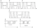
As shown in fig. 3, six different characteristic waveforms are provided for the embodiments of the present application. Of course, other signatures are also available and are not shown here.
For different control signals, different characteristic waveforms are selected, the corresponding relation between each control signal type and the characteristic waveform can be specified in advance and stored in the control unit, when a certain control signal needs to be generated, the corresponding relation is searched to obtain the corresponding waveform characteristic, and then the control signal which is in accordance with the waveform characteristic is generated.
In another embodiment of the present application, as shown in fig. 4, K2 may also be connected in parallel to two ends of the serial branch of L1 and D1, and the operation principle of the circuit shown in fig. 4 is the same as that of the circuit shown in fig. 1, and is not described here again.
In addition, a certain current stress surge exists at the moment of switching of the K2 switch, which can reduce the service life of the switching device, and in order to avoid this phenomenon, in another embodiment of the present application, as shown in fig. 4, a current limiting device, such as a resistor or an inductor, may be added in series with the K2, so as to reduce the current stress surge generated at the moment of switching of the K2 switch. Of course, a current limiting device connected in series with K2 may be added on the basis of the embodiment shown in fig. 2, and will not be described herein again.
In another embodiment of the present application, as shown in fig. 5, the controllable switch circuit is a third controllable switch K3, and the control process of K1 and K3 in this embodiment is the same as the control process of K1 and K2 in fig. 2 and fig. 4, which are not described again here.
The control signal modulation circuit provided by the embodiment is realized based on a typical Boost circuit, a second controllable switch is added on the basis of the typical Boost circuit, when the voltage on the first capacitor is lower than a first voltage threshold value, the second controllable switch is controlled to be conducted, so that the second capacitor charges the first capacitor, and the on-off state of the first controllable switch is controlled until the voltage on the first capacitor reaches the first voltage threshold value, so that a control signal with a preset characteristic waveform is generated on the first capacitor. According to the scheme, the modulation signal with the preset characteristic waveform is generated through the charging and discharging process of the first capacitor in the Boost circuit, so that a special signal generator is not needed, a PLC communication module is not needed, and the hardware cost is low. And compared with a wireless communication mode, the control signal generated by the scheme is not influenced by distance and has no crosstalk phenomenon, and no special requirement is made on the installation site topography.
In the above embodiment, C1 is charged by C2 in the DC/DC boost circuit to bring the voltage of C1 to the voltage level required to generate the preset signature waveform. In another embodiment of the present application, C1 may also be charged by a dc power supply circuit.
Referring to fig. 6, a schematic diagram of another control signal modulation circuit provided in the embodiment of the present application is shown, the modulation circuit provided in the embodiment is implemented based on a DC/DC boost circuit, and a difference between the modulation circuit and the embodiments shown in fig. 2, fig. 4, and fig. 5 is that the embodiment uses a DC power supply circuit as a charging energy source of C1.
As shown in fig. 6, the control signal modulation circuit includes a DC power supply circuit 110, a second unidirectional one-way device D2, a fourth controllable switch K4, a DC/DC boost circuit 120, and a control unit.
In this embodiment, the DC/DC boost circuit 120 may adopt any one of the DC/DC boost topologies shown in fig. 2, fig. 4, and fig. 5, which is not described herein again. The present embodiment will be described by taking the circuit shown in fig. 2 as an example of the DC/DC boost circuit 120.
The output end of the DC power supply circuit 110 is connected to the input port of the DC/DC boost circuit 120 after being serially connected to the fourth controllable switch K4 and the second unidirectional conducting device D2 in sequence.
In this embodiment, the connection direction of D2 enables the electric energy output by the DC power supply circuit to flow to the input port of the DC/DC boost circuit, thereby preventing energy from being transmitted reversely
In an embodiment of the present application, the dc power supply circuit 110 may be implemented by an inverter circuit, and an ac side of the inverter circuit is connected to an ac power source.
When the voltage of C1 is greater than or equal to the first voltage threshold, C1 generates a control signal with a preset characteristic waveform by controlling at least one of the duty cycle and the switching frequency of the switching control signal of K1.
In one possible implementation manner of the present application, when the voltage at C1 is lower than the first voltage threshold, the control K4 is closed to enable the dc power supply circuit 110 to charge the C1.
In another possible implementation manner of the present application, after the control K1 is turned off, the control K4 is closed, and the dc power supply circuit charges the C1.
In another embodiment of the present application, in order to avoid the voltage at C2 from exceeding the safety threshold, when the voltage at C2 is detected to be higher than the second voltage threshold, K2 is controlled to close, so that C2 is discharged, and the risk of overvoltage of C2 is reduced.
Of course, in other embodiments, after the voltage at C2 exceeds the second voltage threshold, the dc load (e.g., a fan, etc.) in the circuit may also be controlled to operate, consuming the energy of C2, which may also reduce the risk of overvoltage of C2.
In an embodiment of the present application, in an application scenario where the control signal modulation circuit is applied to an inverter, the dc power supply circuit 110 may be a power supply circuit existing in the inverter, for example, a power supply circuit supplying power to its own dc load (e.g., a fan, etc.), wherein the power supply voltage may be +24V, etc. Of course, in other embodiments, a separate dc power supply may be used, which is independent from the original dc power supply circuit of the inverter itself, and is not described herein again.
In the control signal modulation circuit provided by this embodiment, the dc power supply circuit is used as an energy source for charging the C1, and when the voltage across the first capacitor is lower than the first voltage threshold, the fourth controllable switch circuit is controlled to be turned on, so that the dc power supply circuit charges the first capacitor. When the voltage of the first capacitor reaches a first voltage threshold value, the switching state of the first controllable switch is controlled to control the charging and discharging state of the first capacitor, so that a control signal with a preset characteristic waveform is generated on the first capacitor. According to the scheme, the first capacitor is charged by the direct-current power supply circuit, and the influence on the C2 is avoided, so that the reliability of the DC/DC booster circuit is improved.
On the other hand, the embodiment of the application also provides an inverter applying the control signal modulation circuit.
Referring to fig. 7, a schematic structural diagram of an inverter provided in the embodiment of the present application is shown, and the embodiment takes a single-input inverter as an example for description.
As shown in fig. 7, the inverter includes a control signal modulation circuit 210, an inverter circuit 220, and an inverter controller;
the control signal modulation circuit 210 is obtained by adding a second controllable switch K2 to the existing Boost circuit of the inverter, that is, the control signal modulation circuit 210 is implemented by using the circuit shown in fig. 2. The Boost circuit comprises C1, L1, K1, D1 and C2.
In this embodiment, K2 is connected in parallel to the two ends of D1 in the Boost circuit, the output port of the Boost circuit is connected to the dc port of the inverter circuit 220, and the input port of the Boost circuit is used for connecting the photovoltaic string.
And the inversion controller obtains a control signal generation instruction and sends the control signal generation instruction to a control unit in the control signal modulation circuit.
And the control unit is used for controlling the K2 to be turned off and controlling the switching state of the K1 when the voltage of the C1 is greater than or equal to the first voltage threshold value, so that the C1 generates a control signal of a preset characteristic waveform.
The control signal is used for enabling the control unit in the photovoltaic string to analyze to obtain a corresponding control instruction and executing the control instruction.
The control unit is further used for controlling the K2 to close to enable the C2 to charge the C1 when the voltage of the C1 is lower than a first voltage threshold value.
In addition, the control unit may be integrated into the inverter controller, or may be a control unit of an independent inverter controller.
In an application scenario, the inverter needs to generate a control signal for controlling the photovoltaic module to be turned on or off, and the control unit is specifically configured to:
when the photovoltaic string is in a conducting state, the voltage across the C1 is the voltage U1 of the photovoltaic string, and U1 is greater than 0. At this time, if the inverter controller obtains a shutdown instruction (for example, generated after detecting that the external DI interface receives a trigger signal of a corresponding button), the inverter is shut down, and meanwhile, the inverter controller generates a shutdown signal to generate an instruction and sends the instruction to the control unit in the control signal modulation circuit. After receiving a turn-off signal generation instruction, the control unit controls K2 to be turned off and K1 to be turned on, and due to the fact that C1 is connected in parallel between the positive pole and the negative pole of the photovoltaic string, L1 is connected in parallel with C1, C1 discharges through L1, and the voltage on C1 drops; when K1 is turned off, the string charges C1 and the voltage on C1 rises. Alternatively, K2 may be controlled to close, charging C1 from C2, to increase the voltage on C1. And controlling the switching state of the K1 according to the preset switching control signal duty ratio and the switching frequency, so that the turn-off control signal of the first preset characteristic waveform can be obtained at the C1.
When the photovoltaic string is in an off state, the voltage on the C1 is almost 0, and when the inverter controller receives the conduction command, the inverter controller generates a conduction signal to generate a command and sends the command to the control unit. Because the photovoltaic string is in the off state and cannot be charged for C1 through the photovoltaic string, after receiving the on signal command, the control unit needs to precharge the dc bus through the ac side grid to boost the dc bus voltage, then controls the K1 to be off, and controls the K2 to be on, at this time, the C2 charges the C1, and when the voltage on the C1 reaches the first voltage threshold, the on-off state of the K1 is controlled, and then the on control signal of the second preset characteristic waveform can be obtained on the C1.
The waveform of the shutdown control signal may be any one of the characteristic waveforms in fig. 3, and may of course be other characteristic waveforms not shown in fig. 3; the on control signal may have other waveform characteristics different from those of the off control signal, which is not limited in this application.
In another embodiment of the present application, in order to reduce the current stress impact generated at the switching moment of K2, a current limiting device, such as a resistor or an inductor, may be added in series with K2.
In another embodiment of the present application, as shown in fig. 8, K2 (or the series branch of K2 and the current limiting device) may also be connected in parallel across the series branch of L1 and D1, and the modulation process for generating the control signal is the same as the modulation process of the inverter shown in fig. 7, and will not be described herein again.
In another application scenario of the present application, the inverter includes a plurality of sets of dc input terminals, and the following description will take two pairs of input terminals as an example.
As shown in fig. 9, the output ports of the two Boost circuits are connected in parallel, that is, the positive and negative output terminals of the first Boost circuit 310 are respectively connected to the positive and negative output terminals of the second Boost circuit 320. Furthermore, the two Boost circuits share one controllable switch K2 (i.e. the second controllable switch), the current limiting device.
One end of the K2 is connected to positive output ends of the first Boost circuit 310 and the second Boost circuit 320, the other end of the K2 is connected to a positive input end of the first Boost circuit 310 through the D2, and meanwhile, the other end of the K2 is also connected to a positive input end of the second Boost circuit 320 through the D21.
In another embodiment of the present application, the second controllable switch K2 is connected in parallel to two ends of the first unidirectional conducting device of each Boost circuit, as shown in fig. 10, one end of K2 is connected to the positive output end of each Boost circuit, the other end of K2 is connected to the common end of L1 and D1 in the first Boost circuit 310 through D2, and meanwhile, the other end of K2 is also connected to the common end of L2 and D11 in the second Boost circuit 320 through D21.
The functions of D2 and D21 in fig. 9 and 10 are unidirectional conduction, which only allows energy to flow from C2 to C1, and only allows energy to flow from C21 to C11, preventing power in other Boost circuits from flowing to the present Boost circuit.
In the circuits of the inverters shown in fig. 9 and 10, the respective Boost circuits share the K2 and the current limiting device, and therefore, the hardware cost is further reduced.
In the inverter provided by the embodiment, control signals with different waveform characteristics are obtained on the first capacitor connected in parallel with the input port of the Boost circuit by controlling the switching state of the controllable switch in the Boost circuit; when the voltage of the first capacitor is lower than the first voltage threshold value, the second controllable switch is controlled to be closed so that the second capacitor charges the first capacitor, and therefore the waveform characteristics generated by the first capacitor are not affected. The scheme utilizes the improved Boost circuit to modulate to obtain a corresponding control signal, and transmits the control signal through the original transmission line. The control signal transmission of the scheme is not influenced by distance and has no crosstalk phenomenon, no special requirements are required on the site topography of the installation site, and a PLC communication module or an independent signal generator is not required to be arranged, so that the hardware cost is low.
Corresponding to the control signal modulation circuit shown in fig. 6, the embodiment of the present application further provides an inverter applying the modulation circuit.
Referring to fig. 11, a schematic structural diagram of another inverter provided in an embodiment of the present application is shown, where the inverter includes: control signal modulation circuit 410, boost circuit 420 and inverter circuit 430.
The control signal modulation circuit 410 includes a dc power supply circuit 411, a controllable switch K, a third one-way conduction device D, and a control unit.
The dc output port of the dc power supply circuit 411 is connected to the dc input port of the boost circuit 420 after being connected in series with K and D in sequence, and the ac end of the dc power supply circuit 411 is connected to an ac power supply.
The first controllable switch K1 in the DC/DC boost circuit 420 is controlled by the control unit so that a control signal of a predetermined characteristic waveform is obtained on the first capacitor in the DC/DC boost circuit 420.
When the voltage of C1 in the DC/DC boost circuit 420 is lower than the first voltage threshold, or after the control K1 is turned off, the control K is turned on, so that the DC power supply circuit 411 charges C1, and the voltage on C1 is boosted.
The control unit of the control signal modulation circuit of this embodiment may be integrated in the inverter controller, or may be a control unit of an independent inverter controller.
In the inverter provided by this embodiment, the dc power supply circuit is used as an energy source for charging the first capacitor, and when the voltage on the first capacitor is lower than the first voltage threshold, the fourth controllable switch circuit is controlled to be turned on, so that the dc power supply circuit charges the first capacitor; when the voltage on the first capacitor reaches a first voltage threshold, the switching state of the first controllable switch is controlled to control the charging and discharging state of the first capacitor, so that a control signal with a preset characteristic waveform is generated on the first capacitor. According to the scheme, the direct current power supply circuit is used for charging the first capacitor, the second capacitor is not affected, and the reliability of the inverter is improved.
In another aspect, the embodiment of the application further provides a photovoltaic string control system.
Referring to fig. 12, a schematic structural diagram of a pv string control system provided in an embodiment of the present application is shown, where the embodiment implements control over a pv string based on the inverter shown in fig. 7.
As shown in fig. 12, the pv string control system includes an inverter 610 and a pv string 620;
the photovoltaic group string 620 comprises n photovoltaic modules PV 1-PVn connected in series, and interrupters RSD 1-RSDn connected with the output end of each photovoltaic module;
the n photovoltaic modules are connected in series in sequence by connecting n RSDs (Rapid Shutdown) in series in sequence.
Each of the shutdown devices in the pv string 620 is connected in series to the dc side of the inverter 610, and after receiving the control signal output by the inverter, each of the shutdown devices analyzes the control signal to obtain a corresponding control command and executes an operation corresponding to the control command.
As shown in fig. 13, a schematic diagram of an internal structure of a shutdown device is shown, and the shutdown device includes a parsing module 710, a controller 720, and a switching tube S.
In an application scene of controlling the on or off of the photovoltaic module, the specific control process of the turn-off device is as follows:
when the waveform characteristics of the control signal output by the inverter analyzed by the analysis module 710 conform to the first preset characteristic waveform, the control signal is determined to be a turn-off control signal, and the controller 720 controls the switch tube S to turn off, so that the photovoltaic module connected with S is disconnected from the inverter.
And when the waveform characteristics of the control signal output by the inverter analyzed by the analysis module 710 conform to a second preset characteristic waveform, determining that the control signal is a conduction control signal, and controlling the conduction of the switching tube S by the controller 720, so that the photovoltaic module connected with the switching tube S is connected with the inverter.
In another embodiment of the application, a control device arranged in the photovoltaic module is used for receiving a control signal sent by the inverter, and when the waveform characteristics of the control signal output by the inverter are analyzed to conform to a third preset characteristic waveform, the control signal is determined to be a monitoring signal, and corresponding state data of the photovoltaic module is uploaded to the inverter.
In other embodiments of the present application, the photovoltaic module control system may further implement control over the photovoltaic module based on other inverters provided in the present application (such as the inverters shown in fig. 8 to 11), and a process of analyzing the control signal sent by the inverter on the photovoltaic module side is similar to the above analysis process, and is not described herein again.
According to the photovoltaic module control system provided by the embodiment, the control signal is generated through the improved circuit modulation in the inverter and is transmitted to the photovoltaic module side. The photovoltaic module analyzes the received control signal to obtain a corresponding control instruction, and then corresponding operation is executed according to the control instruction. The transmission of control signals in the system is not influenced by distance and has no crosstalk phenomenon, no special requirements are required for the site situation of an installation site, and a PLC communication module or an independent signal generator is not required to be arranged, so that the hardware cost is low.
While, for purposes of simplicity of explanation, the foregoing method embodiments have been described as a series of acts or combination of acts, it will be appreciated by those skilled in the art that the present invention is not limited by the illustrated ordering of acts, as some steps may occur in other orders or concurrently with other steps in accordance with the invention. Further, those skilled in the art should also appreciate that the embodiments described in the specification are preferred embodiments and that the acts and modules referred to are not necessarily required by the invention.
It should be noted that, in the present specification, the embodiments are all described in a progressive manner, each embodiment focuses on differences from other embodiments, and the same and similar parts among the embodiments may be referred to each other. For the device-like embodiment, since it is basically similar to the method embodiment, the description is simple, and for the relevant points, reference may be made to the partial description of the method embodiment.
The steps in the method of the embodiments of the present application may be sequentially adjusted, combined, and deleted according to actual needs.
The device and the modules and sub-modules in the terminal in the embodiments of the present application can be combined, divided and deleted according to actual needs.
In the several embodiments provided in the present application, it should be understood that the disclosed terminal, apparatus and method may be implemented in other manners. For example, the above-described terminal embodiments are merely illustrative, and for example, the division of a module or a sub-module is only one logical division, and there may be other divisions when the terminal is actually implemented, for example, a plurality of sub-modules or modules may be combined or integrated into another module, or some features may be omitted or not executed. In addition, the shown or discussed mutual coupling or direct coupling or communication connection may be an indirect coupling or communication connection through some interfaces, devices or modules, and may be in an electrical, mechanical or other form.
The modules or sub-modules described as separate parts may or may not be physically separate, and parts that are modules or sub-modules may or may not be physical modules or sub-modules, may be located in one place, or may be distributed over a plurality of network modules or sub-modules. Some or all of the modules or sub-modules can be selected according to actual needs to achieve the purpose of the solution of the present embodiment.
In addition, functional modules or sub-modules in the embodiments of the present application may be integrated into one processing module, or each module or sub-module may exist alone physically, or two or more modules or sub-modules are integrated into one module. The integrated modules or sub-modules can be implemented in the form of hardware, and can also be implemented in the form of software functional modules or sub-modules.
Finally, it should also be noted that, in this document, relational terms such as first and second, and the like are used solely to distinguish one entity or action from another entity or action without necessarily requiring or implying any actual such relationship or order between such entities or actions. Also, the terms "comprises," "comprising," or any other variation thereof, are intended to cover a non-exclusive inclusion, such that a process, method, article, or apparatus that comprises a list of elements does not include only those elements but may include other elements not expressly listed or inherent to such process, method, article, or apparatus. Without further limitation, an element defined by the phrase "comprising an … …" does not exclude the presence of other identical elements in the process, method, article, or apparatus that comprises the element.
The previous description of the disclosed embodiments is provided to enable any person skilled in the art to make or use the present invention. Various modifications to these embodiments will be readily apparent to those skilled in the art, and the generic principles defined herein may be applied to other embodiments without departing from the spirit or scope of the invention. Thus, the present invention is not intended to be limited to the embodiments shown herein but is to be accorded the widest scope consistent with the principles and novel features disclosed herein.
The foregoing is only a preferred embodiment of the present invention, and it should be noted that, for those skilled in the art, various modifications and decorations can be made without departing from the principle of the present invention, and these modifications and decorations should also be regarded as the protection scope of the present invention.