JP5487084B2 - Power supply - Google Patents
Power supply Download PDFInfo
- Publication number
- JP5487084B2 JP5487084B2 JP2010258716A JP2010258716A JP5487084B2 JP 5487084 B2 JP5487084 B2 JP 5487084B2 JP 2010258716 A JP2010258716 A JP 2010258716A JP 2010258716 A JP2010258716 A JP 2010258716A JP 5487084 B2 JP5487084 B2 JP 5487084B2
- Authority
- JP
- Japan
- Prior art keywords
- voltage
- power supply
- power
- switching
- switching operation
- Prior art date
- Legal status (The legal status is an assumption and is not a legal conclusion. Google has not performed a legal analysis and makes no representation as to the accuracy of the status listed.)
- Expired - Fee Related
Links
Images


Classifications
-
- H—ELECTRICITY
- H02—GENERATION; CONVERSION OR DISTRIBUTION OF ELECTRIC POWER
- H02M—APPARATUS FOR CONVERSION BETWEEN AC AND AC, BETWEEN AC AND DC, OR BETWEEN DC AND DC, AND FOR USE WITH MAINS OR SIMILAR POWER SUPPLY SYSTEMS; CONVERSION OF DC OR AC INPUT POWER INTO SURGE OUTPUT POWER; CONTROL OR REGULATION THEREOF
- H02M3/00—Conversion of dc power input into dc power output
- H02M3/02—Conversion of dc power input into dc power output without intermediate conversion into ac
- H02M3/04—Conversion of dc power input into dc power output without intermediate conversion into ac by static converters
- H02M3/10—Conversion of dc power input into dc power output without intermediate conversion into ac by static converters using discharge tubes with control electrode or semiconductor devices with control electrode
- H02M3/145—Conversion of dc power input into dc power output without intermediate conversion into ac by static converters using discharge tubes with control electrode or semiconductor devices with control electrode using devices of a triode or transistor type requiring continuous application of a control signal
- H02M3/155—Conversion of dc power input into dc power output without intermediate conversion into ac by static converters using discharge tubes with control electrode or semiconductor devices with control electrode using devices of a triode or transistor type requiring continuous application of a control signal using semiconductor devices only
- H02M3/156—Conversion of dc power input into dc power output without intermediate conversion into ac by static converters using discharge tubes with control electrode or semiconductor devices with control electrode using devices of a triode or transistor type requiring continuous application of a control signal using semiconductor devices only with automatic control of output voltage or current, e.g. switching regulators
- H02M3/158—Conversion of dc power input into dc power output without intermediate conversion into ac by static converters using discharge tubes with control electrode or semiconductor devices with control electrode using devices of a triode or transistor type requiring continuous application of a control signal using semiconductor devices only with automatic control of output voltage or current, e.g. switching regulators including plural semiconductor devices as final control devices for a single load
-
- H—ELECTRICITY
- H02—GENERATION; CONVERSION OR DISTRIBUTION OF ELECTRIC POWER
- H02M—APPARATUS FOR CONVERSION BETWEEN AC AND AC, BETWEEN AC AND DC, OR BETWEEN DC AND DC, AND FOR USE WITH MAINS OR SIMILAR POWER SUPPLY SYSTEMS; CONVERSION OF DC OR AC INPUT POWER INTO SURGE OUTPUT POWER; CONTROL OR REGULATION THEREOF
- H02M7/00—Conversion of ac power input into dc power output; Conversion of dc power input into ac power output
- H02M7/02—Conversion of ac power input into dc power output without possibility of reversal
- H02M7/04—Conversion of ac power input into dc power output without possibility of reversal by static converters
- H02M7/12—Conversion of ac power input into dc power output without possibility of reversal by static converters using discharge tubes with control electrode or semiconductor devices with control electrode
- H02M7/21—Conversion of ac power input into dc power output without possibility of reversal by static converters using discharge tubes with control electrode or semiconductor devices with control electrode using devices of a triode or transistor type requiring continuous application of a control signal
- H02M7/217—Conversion of ac power input into dc power output without possibility of reversal by static converters using discharge tubes with control electrode or semiconductor devices with control electrode using devices of a triode or transistor type requiring continuous application of a control signal using semiconductor devices only
- H02M7/2176—Conversion of ac power input into dc power output without possibility of reversal by static converters using discharge tubes with control electrode or semiconductor devices with control electrode using devices of a triode or transistor type requiring continuous application of a control signal using semiconductor devices only comprising a passive stage to generate a rectified sinusoidal voltage and a controlled switching element in series between such stage and the output
Landscapes
- Engineering & Computer Science (AREA)
- Power Engineering (AREA)
- Dc-Dc Converters (AREA)
Description
本発明は、電力に関する情報を生成する機能を有した電源装置に係る。 The present invention relates to a power supply device having a function of generating information about power.
電力測定は、一般に、電圧測定回路によって測定された電圧値と、電流測定回路によって測定された電流値とを演算することによって行われる。すなわち、電圧測定回路と電流測定回路が必要になる。 In general, power measurement is performed by calculating a voltage value measured by a voltage measurement circuit and a current value measured by a current measurement circuit. That is, a voltage measurement circuit and a current measurement circuit are required.
なお、特許文献1には、AC/DCアダプタの整流ブリッジ・ダイオードに供給される交流電圧および交流電流を電流センス抵抗および電圧センス抵抗で検出し、これらのセンス抵抗による検出値を乗算して電力値を求める手法が紹介されている。
In
また、特許文献2には、スイッチング電源回路において、ON状態のスイッチングトランジスタにおける電圧降下を測定して電流を求める手法が紹介されている。
一般的に電力測定には電圧測定回路と電流測定回路を対象回路に追加する必要がある。このため、コスト等の増大を招くことになる。 In general, it is necessary to add a voltage measurement circuit and a current measurement circuit to the target circuit for power measurement. For this reason, an increase in cost etc. will be caused.
本発明は、電力に関連する情報をコスト等が削減された態様で生成可能な電源装置を提供することを目的とする。 An object of this invention is to provide the power supply device which can produce | generate the information relevant to electric power in the aspect by which cost etc. were reduced.
本発明の第1の態様に係る電源装置は、電圧入力端部に印加された入力電圧を所定電圧値の電圧に変換する電圧変換を行い、前記電圧変換後の電圧を電圧出力端部に出力する電源回路と、前記電圧出力端部から出力される電力に関連した電力情報を生成する電力情報生成手段とを備え、前記電源回路は、スイッチング動作によって前記電圧入力端部の側の電圧に対するチョッピングを行うスイッチング手段と、前記スイッチング手段の前記スイッチング動作を制御する制御回路とを含み、前記電力情報生成手段は、前記スイッチング動作の内容に基づいて前記電力情報を生成し、前記制御回路は、スイッチング制御信号を前記スイッチング手段に与えることによって前記スイッチング動作を制御し、前記電力情報生成手段は、前記スイッチング動作の内容を少なくとも含む所定情報と前記電力情報との関係が規定された導出手段を有し、前記スイッチング制御信号を取得し、前記スイッチング制御信号から得られる前記スイッチング動作の内容を前記導出手段に当てはめることによって前記電力情報を導出し、前記チョッピングが施された後の電圧を検出するように設けられた電圧検出器をさらに備え、前記所定情報は、前記電圧検出器による検出箇所の電圧値をさらに含み、前記電力情報生成手段は、前記電圧検出器によって検出された電圧値と、前記スイッチング動作の内容とを前記導出手段に当てはめることによって前記電力情報を導出し、前記制御回路は、前記電圧検出器によって検出された前記電圧値に基づいて前記スイッチング動作をフィードバック制御する。 A power supply apparatus according to a first aspect of the present invention performs voltage conversion for converting an input voltage applied to a voltage input end to a voltage having a predetermined voltage value, and outputs the voltage after the voltage conversion to a voltage output end. And a power information generating means for generating power information related to power output from the voltage output end, the power supply circuit chopping the voltage on the voltage input end side by switching operation Switching means for performing switching, and a control circuit for controlling the switching operation of the switching means, wherein the power information generating means generates the power information based on the contents of the switching operation, and the control circuit is configured to perform switching. The switching operation is controlled by applying a control signal to the switching means, and the power information generating means is A derivation unit that defines a relationship between predetermined information including at least operation content and the power information; obtains the switching control signal; and transmits the switching operation content obtained from the switching control signal to the derivation unit. The power information is derived by fitting, and further provided with a voltage detector provided to detect the voltage after the chopping is performed, and the predetermined information includes a voltage value at a location detected by the voltage detector. Further, the power information generation means derives the power information by applying the voltage value detected by the voltage detector and the content of the switching operation to the derivation means, and the control circuit The switching operation is feedback-controlled based on the voltage value detected by the detector .
また、第2の態様に係る電源装置は、上記の第1の態様に係る電源装置であって、前記電圧検出器は前記電圧出力端部の電圧を検出するように設けられている。 Moreover, the power supply device which concerns on a 2nd aspect is a power supply device which concerns on said 1st aspect, Comprising: The said voltage detector is provided so that the voltage of the said voltage output terminal part may be detected.
また、第3の態様に係る電源装置は、電圧入力端部に印加された入力電圧を所定電圧値の電圧に変換する電圧変換を行い、前記電圧変換後の電圧を電圧出力端部に出力する電源回路と、前記電圧出力端部から出力される電力に関連した電力情報を生成する電力情報生成手段とを備え、前記電源回路は、スイッチング動作によって前記電圧入力端部の側の電圧に対するチョッピングを行うスイッチング手段と、前記スイッチング手段の前記スイッチング動作を制御する制御回路とを含み、前記電力情報生成手段は、前記スイッチング動作の内容に基づいて前記電力情報を生成し、前記制御回路は、スイッチング制御信号を前記スイッチング手段に与えることによって前記スイッチング動作を制御し、前記電力情報生成手段は、前記スイッチング動作の内容を少なくとも含む所定情報と前記電力情報との関係が規定された導出手段を有し、前記スイッチング制御信号を取得し、前記スイッチング制御信号から得られる前記スイッチング動作の内容を前記導出手段に当てはめることによって前記電力情報を導出し、前記電源回路は、DC/DCコンバータであり、前記所定情報は、前記スイッチング動作の内容のみを含み、前記電力情報生成手段は、前記導出手段を用いて、前記スイッチング制御信号から得られる前記スイッチング動作の内容のみから前記電力情報を生成する。 Moreover, the power supply device according to the third aspect performs voltage conversion for converting the input voltage applied to the voltage input end to a voltage having a predetermined voltage value, and outputs the voltage after the voltage conversion to the voltage output end. A power information generation means for generating power information related to the power output from the voltage output end, and the power supply circuit chops the voltage on the voltage input end side by a switching operation. Switching means for performing, and a control circuit for controlling the switching operation of the switching means, wherein the power information generating means generates the power information based on the contents of the switching operation, and the control circuit is configured to perform switching control. The switching operation is controlled by providing a signal to the switching means, and the power information generating means is configured to control the switching operation. A derivation unit that defines a relationship between the predetermined information including at least the content of the operation and the power information, obtains the switching control signal, and transmits the content of the switching operation obtained from the switching control signal to the derivation unit. The power information is derived by fitting, the power supply circuit is a DC / DC converter, the predetermined information includes only the content of the switching operation, and the power information generation means uses the derivation means, The power information is generated only from the content of the switching operation obtained from the switching control signal.
また、第4の態様に係る電源装置は、上記の第1ないし第3の態様のうちのいずれか1つに係る電源装置であって、前記電圧入力端部に通じる電力線を利用して電力線通信(PLC)を行う。 Moreover, the power supply device which concerns on a 4th aspect is a power supply device which concerns on any one of said 1st thru | or 3rd aspect, Comprising: Power line communication using the power line which leads to the said voltage input terminal part (PLC) is performed.
また、第5の態様に係る電源装置は、上記の第1または第2の態様に係る電源装置であって、前記電圧入力端部に通じる電力線を利用して電力線通信(PLC)を行い、前記電圧検出器によって検出された前記電圧値から、他の装置によって前記電力線へ送信されたデータを抽出する受信データ抽出処理を行うPLC処理回路をさらに備える。 A power supply device according to a fifth aspect is the power supply device according to the first or second aspect described above, and performs power line communication (PLC) using a power line leading to the voltage input end, It further includes a PLC processing circuit that performs a reception data extraction process for extracting data transmitted to the power line by another device from the voltage value detected by the voltage detector.
また、第6の態様に係る電源装置は、上記の第4または第5の態様に係る電源装置であって、前記制御回路は前記PLCによる送信データに応じて前記スイッチング動作を変調する。 Moreover, the power supply device which concerns on a 6th aspect is a power supply device which concerns on said 4th or 5th aspect, Comprising: The said control circuit modulates the said switching operation according to the transmission data by said PLC.
上記の第1および第3の態様によれば、電源回路は電圧入力端部の側の電圧に対するチョッピングを利用して電圧変換を行う。当該チョッピング、換言すればスイッチング手段のスイッチング動作によって、電圧変換に供される電荷量が決まり、当該電荷量は電圧出力端部からの出力電流量に相関する。かかる点に着目した第1および第3の態様では、電力情報(電圧出力端部からの出力電力に関連する情報)の生成にスイッチング動作の内容を利用することによって、電流検出器を不要にしている。これにより、コスト、サイズ、消費電力等を削減することができる。 According to the first and third aspects, the power supply circuit performs voltage conversion using chopping for the voltage on the voltage input end side. The amount of charge used for voltage conversion is determined by the chopping, in other words, the switching operation of the switching means, and the amount of charge correlates with the amount of output current from the voltage output end. In the first and third aspects focusing on this point, the current detector is made unnecessary by using the contents of the switching operation to generate the power information (information related to the output power from the voltage output end). Yes. Thereby, cost, size, power consumption, etc. can be reduced.
上記の第1および第3の態様によれば、電力情報生成手段はスイッチング動作の内容をスイッチング制御信号から得る。このため、スイッチング手段の動作状況を実測するための構成を設ける必要がなく、簡易な構成によって電力情報を生成できる。したがって、その分、コスト、サイズ、消費電力等を削減することができる。 According to the first and third aspects, the power information generating unit obtains the content of the switching operation from the switching control signal. For this reason, it is not necessary to provide a configuration for actually measuring the operating state of the switching means, and power information can be generated with a simple configuration. Therefore, cost, size, power consumption, etc. can be reduced accordingly.
上記の第1の態様によれば、電力情報の生成に、チョッピング後の電圧値、換言すれば出力側の電圧値をさらに利用する。このため、電源回路の実動状況が反映されて、電力情報の確度を向上させることができる。 According to the first aspect described above, the voltage value after chopping, in other words, the voltage value on the output side is further used to generate power information. For this reason, the actual situation of the power supply circuit is reflected, and the accuracy of the power information can be improved.
上記の第2の態様によれば、電源回路によって生成された安定的な電圧を利用して、電力情報が生成される。このため、電力情報の確度を向上させることができる。 According to said 2nd aspect, electric power information is produced | generated using the stable voltage produced | generated by the power supply circuit. For this reason, the accuracy of the power information can be improved.
上記の第1の態様によれば、制御回路と電力情報生成手段で電圧検出器を共用することができる。したがって、別々に電圧検出器を設けた構成に比べて、コスト、サイズ、消費電力等を削減することができる。 According to said 1st aspect, a voltage detector can be shared by a control circuit and electric power information generation means. Therefore, cost, size, power consumption, and the like can be reduced as compared with the configuration in which the voltage detector is provided separately.
上記の第3の態様によれば、電力情報の生成に電圧値を利用しない。したがって、電力情報生成のためだけに電圧検出器を設ける必要がないので、その分、コスト、サイズ、消費電力等を削減することができる。 According to said 3rd aspect, a voltage value is not utilized for the production | generation of electric power information. Accordingly, it is not necessary to provide a voltage detector only for generating power information, and accordingly, cost, size, power consumption, and the like can be reduced.
上記の第4および第5の態様によれば、電源装置自身または電源装置に接続される回路がPLCを行うことができる。 According to said 4th and 5th aspect, the power supply device itself or the circuit connected to a power supply device can perform PLC.
上記の第5の態様によれば、PLC処理回路と電力情報生成手段で電圧検出器を共用することができる。したがって、別々に電圧検出器を設けた構成に比べて、コスト、サイズ、消費電力等を削減することができる。 According to said 5th aspect, a voltage detector can be shared by a PLC processing circuit and an electric power information generation means. Therefore, cost, size, power consumption, and the like can be reduced as compared with the configuration in which the voltage detector is provided separately.
上記の第6の態様によれば、スイッチング手段のスイッチング動作を利用してPLCによるデータ送信を行うことが可能である。すなわち、スイッチング手段と制御回路を電源機能とPLC送信機能で共用している。このため、PLC送信用のラインドライバが不要である。したがって、その分、コスト、サイズ、消費電力等を削減することができる。 According to said 6th aspect, it is possible to perform data transmission by PLC using the switching operation of a switching means. That is, the switching means and the control circuit are shared by the power supply function and the PLC transmission function. For this reason, a line driver for PLC transmission is unnecessary. Therefore, cost, size, power consumption, etc. can be reduced accordingly.
<第1の実施の形態>
<電源装置の利用形態>
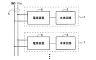
実施の形態1に係る電源装置6の構成例を説明する前に、図1のブロック図を参照して、その利用形態を例示する。
<First Embodiment>
<Usage of power supply device>
Before describing a configuration example of the
図1の例によれば、電源装置6は、電力線5と本体回路2とに接続されて使用される。かかる利用形態において、電源装置6は、電力線5からの供給電圧を所定の電圧値に変換し変換後の電圧を本体回路2へ供給する電源機能と、電源装置6から本体回路2へ供給する電力、換言すれば本体回路2の消費電力に関連した情報である電力情報を生成する電力情報生成機能とを実現する。本体回路2は例えばパーソナルコンピュータ(PC)、各種家電機器、各種電池等に相当する。なお、電源装置6と本体回路2とを接続する配線の本数は図示の例に限定されるものではない。
According to the example of FIG. 1, the
図1の例では、電源装置6と本体回路2とを含んで電源機能付き装置7が構成され、複数の電源機能付き装置7が電力線5に接続されている。電源機能付き装置7によれば、電源装置6が奏する後述の各種効果を享受することができる。
In the example of FIG. 1, a power supply device 7 is configured including the
ここで、電源装置6は、本体回路2と同じ筐体に収容されてもよいし、あるいは、本体回路2とは別個の筐体に収容されてもよい。
Here, the
また、電源装置6は、特定の本体回路2と組み合わされた形態で以て(すなわち電源機能付き装置7の態様で以て)提供されてもよいし、あるいは、電源装置6単体で以て(すなわち種々の本体回路2と後発的に組み合わせ可能な態様で以て)提供されてもよい。
Further, the
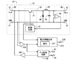
<電源機能>
図2は電源装置6の構成を例示するブロック図である。図2に示すように、電源装置6は上記電源機能を実現する電源回路10を含んでいる。図2に例示の電源回路10は、DC/DCコンバータであり、非絶縁型、スイッチング型および降圧型に分類される。電源回路10は、図2の例によれば、電圧入力端部20と、スイッチング回路30と、ダイオード40と、インダクタ50と、コンデンサ60と、電圧検出器70と、電圧出力端部80とを含んでいる。
<Power supply function>
FIG. 2 is a block diagram illustrating the configuration of the
電圧入力端部20は、電力線5(図1参照)から電圧、換言すれば電力が供給される側の部分であり、図1の例に従えば電源装置6の外部に在る電力線5に接続される外部接続端部にあたる。図2には、電圧入力端部20が入力端子21,22を含み、端子21が接地電位GNDに設定され、端子21,22間に電圧Vin(ここではDC電圧)が印加される場合を例示している。
The voltage
電圧入力端部20に印加された入力電圧Vinが、電源回路10による電圧変換によって、所定の電圧値を有する電圧Voutに変換される。
The input voltage Vin applied to the
スイッチング回路30は、図2の例では、スイッチング手段31と、制御回路32とを含んでいる。
The switching
スイッチング手段31は、そのスイッチング動作によって、電圧入力端部20の側の電圧(図2の構成例では電圧入力端部20に印加される入力電圧Vin)に対してチョッピングを行うための手段である。図2の例ではスイッチング手段31はバイポーラトランジスタによって具現化されている。このため、スイッチング手段31を、バイポーラトランジスタ31またはトランジスタ31とも称することにする。トランジスタ31は、コレクタが入力端子22に接続され、エミッタがダイオード40およびインダクタ50に接続され、ベースが制御回路32に接続されている。
The switching means 31 is means for chopping the voltage on the
ここで、スイッチング手段31としてMOSFET等の各種スイッチング素子や、スイッチング動作を実現可能な各種回路を用いることも可能である。スイッチング手段31は、一般化すれば、一端(トランジスタ31ではコレクタが対応する)と、他端(トランジスタ31ではエミッタが対応する)と、上記の一端と他端との間の導通/非導通状態、換言すればON/OFF状態を制御するための制御信号が入力される制御端(トランジスタ31ではベースが対応する)と有している。制御端への入力信号で以て上記の一端と他端との間の導通/非導通状態が切り替えられることにより、上記一端に印加された電圧がチョッピングされて、上記他端に現れる。 Here, it is also possible to use various switching elements such as MOSFETs and various circuits that can realize the switching operation as the switching means 31. Generally speaking, the switching means 31 is in a conductive / non-conductive state between one end (the collector corresponds to the transistor 31), the other end (the emitter corresponds to the transistor 31), and the one end and the other end. In other words, it has a control terminal (a base corresponds to the transistor 31) to which a control signal for controlling the ON / OFF state is input. The conduction / non-conduction state between the one end and the other end is switched by an input signal to the control end, whereby the voltage applied to the one end is chopped and appears at the other end.
制御回路32は、トランジスタ31のスイッチング動作を制御する。制御回路32は、トランジスタ31のベースに接続されており、パルス状のスイッチング制御信号S31をベースへ印加することによってトランジスタ31のON/OFF状態を制御する。これにより、トランジスタ31による電圧Vinのチョッピングが実行される。
The
なお、説明を簡単にするために、スイッチング制御信号S31のHighレベル(Hレベル)によって、トランジスタ31が導通状態になり、当該導通状態をトランジスタ31のON状態と称することにする。すなわち、スイッチング制御信号S31のHレベルと、トランジスタ31の導通状態と、トランジスタ31のON状態とが互いに対応するものとする。この場合、スイッチング制御信号S31のLowレベル(Lレベル)と、トランジスタ31の非導通状態と、トランジスタ31のOFF状態とが互いに対応する。
For the sake of simplicity, the
制御回路32は例えばスイッチング制御信号S31のHレベルの周期、期間幅等を調整可能に構成されており、これによりトランジスタ31のスイッチング周期(換言すればスイッチング周波数)、ON期間幅(すなわちON状態が持続する期間の時間長さ)等が制御される。これにより、トランジスタ31のスイッチング動作、換言すればトランジスタ31によるチョッピングの具体的形態が制御される。
The
ダイオード40は、カソードがトランジスタ31のエミッタに接続され、アノードが入力端子21に接続されている。ダイオード40は、いわゆる環流ダイオードである。インダクタ50は、一端がダイオード40のカソードに接続され、他端がコンデンサ60の一端に接続されている。コンデンサ60の他端は、ダイオード40のアノードに接続されている。コンデンサ60の上記両端間の電圧が、電圧変換された所望の電圧Voutになる。
The
電圧検出器70は、ここでは、電圧変換後の電圧Vout(したがってチョッピング後の電圧)の検出・測定に利用される。電圧検出器70として例えばA/D(Analog/Digital)コンバータを採用可能であり、このため電圧検出器70をA/Dコンバータ70とも称することにする。
Here, the
A/Dコンバータ70は、図2の例では、一方の入力端がコンデンサ60の上記一端に接続され、他方の入力端がコンデンサ60の上記他端に接続され、出力端が制御回路32に接続されている。これにより、コンデンサ60の両端間の電圧(すなわち電圧変換後の電圧)Voutが検出され、その検出電圧値(換言すれば測定電圧値)がA/D変換されて制御回路32へ与えられる。
In the example of FIG. 2, the A /
電圧出力端部80は、入力電圧Vinから生成された変換電圧Voutを取り出すための部分である。図2には、電圧出力端部80が出力端子81,82を含み、端子81がA/Dコンバータ70の上記他方の入力端に接続され、端子82がA/Dコンバータ70の上記一方の入力端に接続されている場合を例示している。これによれば、端子81が接地電位GNDに設定され、端子81,82間に電圧Voutが現れる。電圧出力端部80は、図1の例では、電源装置6の外部に在る本体回路2に接続される外部接続端部にあたる。
The
電源回路10は概略、次のように動作する。すなわち、入力電圧Vinが、トランジスタ31によってチョッピングされ、インダクタ50とコンデンサ60とによるLCフィルタによって平滑化され、これにより出力電圧Voutになる。これから分かるように、出力電圧Voutは、入力電圧Vinを起源とし、入力電圧Vinに対応する電圧である。なお、一般にスイッチング型の電源回路では、いわゆるリニア型の電源回路とは異なり、電力線5から取り込む電力量(換言すればエネルギー)と、当該電源回路から出力する電力量とが原理的には等しい。
The
出力電圧Voutの電圧値は入力電圧Vinのチョッピングの設定によって、換言すればスイッチング制御信号S31の周期、パルス幅等によって制御可能である。 The voltage value of the output voltage Vout can be controlled by setting the chopping of the input voltage Vin, in other words, by the period of the switching control signal S31, the pulse width, and the like.
そこで、制御回路32は、A/Dコンバータ70による出力電圧Voutの検出値と、出力電圧Voutについて予め与えられた設定値との誤差が小さくなるように、スイッチング制御信号S31のパルス形状を制御する(フィードバック制御)。ここでは、パルス周期を一定にしてパルスのON期間幅(換言すればパルスのデューティ比(=ON期間幅/パルス周期))を制御する、いわゆるパルス幅変調(Pulse Width Modulation;PWM)が採用される場合を例示する。
Therefore, the
このように制御回路32は、トランジスタ31による入力電圧Vinのチョッピングを制御して、所望電圧値を得るための電圧変換を行う。
In this way, the
なお、上記フィードバック制御に関し、電圧検出器70としてコンパレータを利用することも可能である。具体的には、コンパレータが、変換後電圧Voutを検出し、当該検出電圧値と電圧Voutの設定値とを比較し、その比較結果に関する信号を制御回路32へ送信するようにしてもよい。つまり、出力電圧Voutの検出値と設定値との比較を制御回路32ではなくコンパレータに行わせてもよい。
Note that a comparator may be used as the
ここで、図3にスイッチング制御信号S31の波形を例示する。図3から分かるように、負荷が大きいほど(換言すれば本体回路2(図1参照)での消費電力が大きいほど)、スイッチング制御信号S31のON期間のパルス幅が長くなる(換言すればパルスのデューティ比(=ON期間幅/パルス周期)が大きくなる)。 Here, FIG. 3 illustrates the waveform of the switching control signal S31. As can be seen from FIG. 3, the greater the load (in other words, the greater the power consumption in the main circuit 2 (see FIG. 1)), the longer the pulse width of the ON period of the switching control signal S31 (in other words, the pulse Duty ratio (= ON period width / pulse period) increases).
<電力情報生成機能>
図2に示すように、電源装置6はさらに、電圧検出器100と、電力情報生成手段310と、電力情報出力端部320とを含んでおり、これらは電力情報生成機能に関連する。なお、図面では「電力情報生成手段」を「電力情報生成」と略記しており、かかる表記方法は他の要素についても用いる場合がある。
<Power information generation function>
As shown in FIG. 2, the
電圧検出器100は、ここでは、電圧入力端部20に印加された入力電圧Vin(したがってチョッピング前の電圧)の検出・測定に利用される。電圧検出器100として例えばA/Dコンバータを採用可能であり、このため電圧検出器100をA/Dコンバータ100とも称することにする。
Here, the
A/Dコンバータ100は、図2の例では、一方の入力端が入力端子22に接続され、他方の入力端が入力端子21に接続され、出力端は電力情報生成手段310に接続されている。これにより、(トランジスタ31によってチョッピングされる前の)入力電圧Vinの電圧値が検出され、その検出電圧値(換言すれば測定電圧値)がA/D変換されて電力情報生成手段310へ入力される。
In the example of FIG. 2, the A /
電力情報生成手段310は、A/Dコンバータ100の出力端と、制御回路32の出力端(スイッチング制御信号S31を出力する端部)と、電力情報出力端部320とに接続されている。これにより、電力情報生成手段310は、A/Dコンバータ100から入力電圧Vinの検出値を取得するとともに、制御回路32からスイッチング制御信号S31を取得し、取得した入力電圧Vinの検出値とスイッチング制御信号S31とに基づいて電力情報PIを生成する。電力情報生成手段310の各種の処理・機能はソフトウェア(換言すればプログラム実行)、ハードウェア回路構成、またはこれらの組み合わせによって具現化可能である。
The power information generation means 310 is connected to the output end of the A /
電力情報PIは、上記のように、電源装置6から本体回路2へ出力される電力に関連した情報であり、換言すれば本体回路2の消費電力に関連した情報である。電力情報PIは、例えば、電源装置6からの出力電力の瞬時値、積算値等であってもよいし、あるいは、これらの値に相関するレベル値であってもよい。また、電力情報PIは、数値だけでなく、例えば上記値と予め設定された値との比較結果を示す情報であってもよい。なお、比較結果情報は例えば、電力が既定上限値を超えている、あるいは規定下限値を下回っている等の通知に利用可能である。
As described above, the power information PI is information related to the power output from the
生成された電力情報PIは、ここでは、電力情報出力端部320へ出力される。すなわち、電力情報PIは、電力情報出力端部320を介して取り出し可能であり、例えば、本体回路2おける消費電力の管理や、電源装置6での表示に供される。また、電力情報PIを電源機能付き装置7(図1参照)の外部へ出力して利用しても構わない。
Here, the generated power information PI is output to the power
なお、図2には電力情報出力端部320が1つの端子で構成される場合を例示しているが、複数の端子によって当該端部320を構成することも可能である。
In addition, although the case where the power information
電力情報生成手段310は次の観点に基づいて構成されている。すなわち、上記のように、電源回路10は電圧入力端部20の側の電圧(ここでは入力電圧Vin)に対するチョッピングを利用して電圧変換を行う。当該チョッピング、換言すればトランジスタ31のスイッチング動作によって、電圧変換に供される電荷量(換言すればエネルギー)が決まり、当該電荷量は電圧出力端部80からの出力電流値に相関する。したがって、トランジスタ31のスイッチング動作の状況を把握すれば、電流検出器を用いなくても、電源回路10からの出力電流に相関した情報を得ることが可能である。かかる観点に鑑み、電力情報生成手段310は、トランジスタ31のスイッチング動作の状況に基づいて電力情報PIを生成する。電力情報生成手段310の具体例を以下に説明する。
The power
電力情報生成手段310は導出手段311を有しており、導出手段311には所定の情報と電力情報PIとの関係が予め規定されている。上記所定情報は、電源装置6の場合、トランジスタ31のスイッチング動作の内容と、A/Dコンバータ100が電圧検出の対象としている箇所の電圧値である。スイッチング動作の内容に関する情報として、ここでは、トランジスタ31のON状態の時間長さを例示する。この場合、導出手段311には、トランジスタ31のON状態の時間長さと、A/Dコンバータ100による検出箇所の電圧値と、電力情報PIとの関係が規定されている。これら3つの情報の関係は例えば実験や回路解析等によって求めることが可能であり、予め求めた関係が導出手段311に与えられている。導出手段311は例えば、ルックアップテーブル(LUT)、プログラム、演算式、演算回路等の態様で以て具現化可能である。
The power
なお、スイッチング動作の内容に関する情報は上記例示に限定されるものではない。例えば、スイッチング動作の周期とデューティ比とを採用することも可能である。 Note that the information regarding the content of the switching operation is not limited to the above example. For example, it is possible to employ the period and duty ratio of the switching operation.
電力情報生成手段310は、導出手段311を利用して電力情報PIを生成する。より具体的には、電力情報生成手段310は、制御回路32からスイッチング制御信号S31を取得するので、当該スイッチング制御信号S31からトランジスタ31の動作内容(ここではON状態の時間長さが例示される)を取得可能である。電力情報生成手段310は、このようにして得られたトランジスタ31のON状態の時間長さを、導出手段311における「トランジスタ31のON状態の時間長さ」に当てはめ、A/Dコンバータ100から取得した入力電圧Vinの検出値を、導出手段311における「A/Dコンバータ100による検出箇所の電圧値」に当てはめる。このように対応する項目を当てはめることによって導出手段311から電力情報PIが導出される。
The power
ここで、トランジスタ31のスイッチング動作の内容は電力線5(図1参照)から取り込む電荷量に相関し、A/Dコンバータ100による検出電圧は電力線5からの供給電圧に相関する。このため、導出手段311は電力線5からの供給電力に基づいて電力情報PIを導出する手段と捉えることが可能である。
Here, the content of the switching operation of the
<効果等>
電源装置6によれば、電力情報PIの生成にトランジスタ31のスイッチング動作の内容を利用することによって、電流検出器を不要にしている。これにより、コスト、サイズ、消費電力等を削減することができる。
<Effects>
According to the
また、電力情報生成手段310はトランジスタ31のスイッチング動作の内容をスイッチング制御信号S31から取得する。これに対し、例えば、トランジスタ31の動作状況を実測する構成を設けることによって、スイッチング動作の内容を取得することも可能である。しかし、スイッチング制御信号S31を利用した方が簡易な構成によって電力情報PIを生成でき、その分、コスト、サイズ、消費電力等を削減することができる。
Further, the power
また、電力情報PIの生成に、トランジスタ31の動作内容だけでなく、A/Dコンバータ100による検出電圧値(より具体的にはチョッピング前の電圧値、換言すれば入力側の電圧値)も利用する。このため、電源回路10の実動状況が反映されて、電力情報PIの確度を向上させることができる。
In addition, not only the operation contents of the
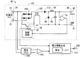
<第2の実施の形態>
図4は第2の実施の形態に係る電源装置6Bの構成を例示するブロック図である。なお、電源装置6Bも本体回路2(図1参照)と組み合わせ可能である。
<Second Embodiment>
FIG. 4 is a block diagram illustrating the configuration of a power supply device 6B according to the second embodiment. The power supply device 6B can also be combined with the main circuit 2 (see FIG. 1).
電源装置6Bは上記電源装置6(図2参照)と類似の構成を有しているが、A/Dコンバータ100(図2参照)が設けられていない。また、電力情報生成手段310はA/Dコンバータ70の出力を取得するように構成されている。また、導出手段311(図2参照)に代えて、導出手段311Bが設けられている。電源装置6Bのその他の構成は基本的に上記電源装置6と同じである。
The power supply device 6B has a configuration similar to that of the power supply device 6 (see FIG. 2), but the A / D converter 100 (see FIG. 2) is not provided. The power
電源装置6Bの電力情報生成手段310は、制御回路32からスイッチング制御信号S31を取得するとともに、A/Dコンバータ70から出力電圧Vout(したがってチョッピング後の電圧)の検出値を取得し、取得したスイッチング制御信号S31と出力電圧Voutの検出値とに基づいて電力情報PIを生成する。すなわち、A/Dコンバータ100(図2参照)の検出電圧値に代えて、電源回路10に既存のA/Dコンバータ70の検出電圧値を利用する。
The power
かかる態様に対応して、導出手段311Bには、A/Dコンバータ100(図2参照)が電圧検出の対象としている箇所の電圧値Vinの代わりに、A/Dコンバータ70が電圧検出の対象としている箇所の電圧値Voutが採用されている。つまり、導出手段311Bにおいて電力情報PIと関連付けられる所定情報は、トランジスタ31のスイッチング動作の内容と、A/Dコンバータ70が電圧検出の対象としている箇所の電圧値Voutである。
Corresponding to such an aspect, the derivation means 311B includes the A /
なお、A/Dコンバータ70,100による検出対象電圧値Vout,Vinが相関を有することは、実験や回路解析等を通じて把握可能である。このため、上記のように導出手段311Bを電圧値Vinの代わりに電圧値Voutを採用した構成とすることができる。かかる点に鑑みれば、電圧入力端部20および電圧出力端部80以外の箇所の電圧を利用して電力情報PIを生成することも可能である。
The fact that the detection target voltage values Vout and Vin by the A /
電力情報生成手段310は、導出手段311Bを上記導出手段311と同様に利用して、電力情報PIを生成する。
The power
電源装置6Bによれば、上記電源装置6(図2参照)と同様に、電流検出器が不要であるので、その分、コスト、サイズ、消費電力等を削減することができる。 According to the power supply device 6B, since a current detector is unnecessary as in the case of the power supply device 6 (see FIG. 2), the cost, size, power consumption, and the like can be reduced accordingly.
また、電力情報生成手段310は、上記電源装置6の場合と同様に、トランジスタ31のスイッチング動作の内容をスイッチング制御信号S31から取得する。したがって、構成の簡易化、コスト、サイズ、消費電力等の削減を図ることができる。
Further, the power
また、電力情報PIの生成に、トランジスタ31の動作内容だけでなく、A/Dコンバータ70による検出電圧値(より具体的にはチョッピング後の電圧値、換言すれば出力側の電圧値)も利用する。このため、電源回路10の実動状況が反映されて、電力情報PIの確度を向上させることができる。
Further, not only the operation contents of the
また、電圧出力端部80の出力電圧Voutを利用して電力情報PIが生成される。入力電圧Vinは例えばトランジスタ31や電力線5に接続された他の装置の動作によるノイズを含む場合があるのに対し、出力電圧Voutは電源回路10によって生成された安定的な電圧である。かかる安定的な電圧Voutを利用して電力情報PIを生成することにより、電力情報PIの確度を向上させることができる。
Further, the power information PI is generated using the output voltage Vout of the
また、制御回路32と電力情報生成手段310でA/Dコンバータ70を共用しているので、別々に電圧検出器を設けた構成に比べてコスト、サイズ、消費電力等を削減することができる。
Further, since the A /
<第3の実施の形態>
図5は第3の実施の形態に係る電源装置6Cの構成を例示するブロック図である。なお、電源装置6Cも本体回路2(図1参照)と組み合わせ可能である。
<Third Embodiment>
FIG. 5 is a block diagram illustrating the configuration of a
電源装置6Cは上記電源装置6(図2参照)と類似の構成を有しているが、A/Dコンバータ100(図2参照)が設けられていない。また、導出手段311(図2参照)に代えて、導出手段311Cが設けられている。電源装置6Cのその他の構成は基本的に上記電源装置6と同じである。
The
電源装置6Cの電力情報生成手段310は、制御回路32からスイッチング制御信号S31を取得するが、上記電源装置6,6B(図2および図4参照)とは異なりA/Dコンバータ100,70による検出電圧値を取得しない。このため、電力情報生成手段310は、取得したスイッチング制御信号S31のみに基づいて電力情報PIを生成する。
The power information generation means 310 of the
かかる態様に対応して、導出手段311Cは、トランジスタ31のスイッチング動作の内容と電力情報PIとの関係を規定している。つまり、導出手段311Cにおいて電力情報PIと関連付けられる所定情報は、トランジスタ31のスイッチング動作の内容のみである。
Corresponding to such an aspect, the deriving unit 311C defines the relationship between the content of the switching operation of the
電力情報生成手段310は、導出手段311Cを上記導出手段311と同様に利用して、電力情報PIを生成する。
The power
電源装置6Cによれば、上記電源装置6(図2参照)と同様に、電流検出器が不要であるので、その分、コスト、サイズ、消費電力等を削減することができる。
According to the
また、電力情報生成手段310は、上記電源装置6の場合と同様に、トランジスタ31のスイッチング動作の内容をスイッチング制御信号S31から取得する。したがって、構成の簡易化、コスト、サイズ、消費電力等の削減を図ることができる。
Further, the power
また、電力情報PIの生成に電圧値を利用しないので、電力情報生成のためだけに電圧検出器を設ける必要がない。よって、その分、コスト、サイズ、消費電力等を削減することができる。 Further, since the voltage value is not used for generating the power information PI, it is not necessary to provide a voltage detector only for generating the power information. Therefore, cost, size, power consumption, etc. can be reduced accordingly.
なお、DC/DCコンバータである電源回路10によれば、入力電圧Vinは設計上既知のDC電圧であるので、電力線5から取り込む電力量はトランジスタ31の動作内容のみから把握可能である。かかる点に鑑み、電源装置6Cでは、電力情報PIの生成に電圧値を利用しなくても、電力情報PIを生成できるのである。
According to the
<第4の実施の形態>
図6は第4の実施の形態に係る電源装置6Dの構成を例示するブロック図である。なお、電源装置6Dも本体回路2(図1参照)と組み合わせ可能である。電源装置6Dは、上記の電源機能および電力情報生成機能に加え、電力線5を利用したPLCを行う通信機能を有している。
<Fourth embodiment>
FIG. 6 is a block diagram illustrating the configuration of a
電源装置6Dは、上記電源装置6(図2参照)に、データ入力端部91と、データ出力端部92と、PLC処理回路110と、ラインドライバ350とを追加した構成を有している。
The
データ入力端部91は電力線5(図1参照)へ送信するデータDtが入力される部分である。例えば本体回路2(図1参照)が電源装置6Dを利用してPLCを行う場合、データ入力端部91は本体回路2に接続される外部接続端部にあたり、本体回路2からデータ入力端部91へ送信データDtが与えられる。
The
データ出力端部92は電力線5(図1参照)から受信したデータDrを取り出すための部分である。例えば本体回路2(図1参照)が電源装置6Dを利用してPLCを行う場合、データ出力端部92は本体回路2に接続される外部接続端部にあたり、データ出力端部92を介して本体回路2へ受信データDrが与えられる。
The data
なお、図6にはデータ入力端部91が1つの端子で構成される場合を例示しているが、複数の端子によってデータ入力端部91を構成することも可能である。データ出力端部92についても同様である。
FIG. 6 illustrates the case where the
PLC処理回路110は、データ入力端部91と、データ出力端部92と、ラインドライバ350の入力端と、A/Dコンバータ100の出力端とに接続されている。
The
PLC処理回路110は、PLCに関する各種処理(送信処理と受信処理に大別される)を行う。
The
送信処理においてPLC処理回路110は、例えば、データ入力端部91へ入力された送信データDtに対して所定の送信ベースバンド処理を施すことによってベースバンド信号を生成する。
In the transmission process, the
上記送信ベースバンド処理として例えば、制御に関する情報(例えば誤り制御の情報)を付加する処理、データを所定サイズに分割する処理等が挙げられる。送信処理の内容は、予め採用されたプロトコルに応じて規定される。 Examples of the transmission baseband process include a process of adding information related to control (for example, error control information), a process of dividing data into a predetermined size, and the like. The content of the transmission process is defined according to a protocol adopted in advance.
PLC処理回路110は生成したベースバンド信号を、必要に応じてD/A(Digital/Analog)変換した後、ラインドライバ350へ出力する。
The
ラインドライバ350の出力端は図6の例では電圧入力端子22に接続されている。ラインドライバ350が、PLC処理回路110から取得したベースバンド信号に応じて(従って送信データDtに応じて)自身の出力電圧値を制御することにより、送信データDtが電力線5(図1参照)へ送信される。
The output terminal of the
なお、PLC処理回路110を経由せずに送信データDtをそのままベースバンド信号にすることも可能であるが、PLC処理回路110において各種データ加工を施すことによって、通信の信頼性が向上する。
Note that the transmission data Dt can be directly used as a baseband signal without going through the
他方、受信処理においてPLC処理回路110は、例えば、A/Dコンバータ100の出力信号(すなわち入力電圧Vinの検出電圧)に対して所定の受信ベースバンド処理を施すことによって、他の装置によって電力線5(図1参照)へ送信されたデータを抽出する(受信データ抽出処理)。
On the other hand, in the reception process, the
上記受信ベースバンド処理として例えば、A/Dコンバータ100の出力信号からベースバンド信号を抽出する処理、ベースバンド信号に付加されている制御に関する情報(例えば誤り制御の情報)に応じた処理、分割送信されたデータの復元処理、受信したデータが当該電源装置6D宛のデータであるかの判断処理等が挙げられる。受信処理の内容は、予め採用されたプロトコルに応じて規定される。
As the reception baseband processing, for example, processing for extracting a baseband signal from the output signal of the A /
電源装置6Dによれば、上記電源装置6(図2参照)と同様の効果を得ることができるとともに、電源装置6D自身または電源装置6Dに接続される本体回路2等がPLCを行うことができる。
According to the
また、PLC処理回路110と電力情報生成手段310でA/Dコンバータ100を共用しているので、別々に電圧検出器を設けた構成に比べてコスト、サイズ、消費電力等を削減することができる。
In addition, since the A /
なお、上記各種構成を応用して、上記電源装置6B,6C(図4および図5参照)等にPLC機能を付加することも可能である。
It is also possible to add a PLC function to the
また、PLC処理回路110がA/Dコンバータ70の検出電圧に対して受信データ抽出処理を行うように構成することも可能である。
Further, the
この場合、A/Dコンバータ70は、トランジスタ31の接続位置から見て電圧出力端部80の側に接続されており、A/Dコンバータ100(図6参照)とは異なり、回路上、電圧入力端部20から離れた位置に接続されている。このため、A/Dコンバータ70による検出電圧によれば、上記電源装置6Dと同様の精度で受信データ抽出処理を行うは難しい場合がある。
In this case, the A /
そのような場合、PLC処理回路110が、A/Dコンバータ70による検出電圧(入力電圧Vinを起源とし、入力電圧Vinに対応する)から入力電圧Vinを推定し、当該推定電圧に対して受信データ抽出処理を行えばよい。かかる入力電圧Vinの推定は、電圧入力端部20とA/Dコンバータ70との間の回路構成の情報に基づいて行うことが可能である。回路構成の情報は例えば、当該回路構成を数式化することによって、あるいは、当該回路構成について入出力値の対応関係を求めてデータベース化することによって、PLC処理回路110に与えることが可能である。なお、回路構成の情報に係る数式、データベース等は、ハードウェア(例えばデジタルフィルタ)によって提供してもよいし、ソフトウェア(換言すればプログラム処理)によって提供されてもよい。
In such a case, the
入力電圧推定処理を利用することにより、電圧入力端部20とA/Dコンバータ70との間に回路が介在する場合であっても、受信データ抽出処理の精度、すなわちデータ受信の信頼性を確保することができる。換言すれば、データ受信に利用するA/Dコンバータの接続位置の自由度を高くすることができる。
By using the input voltage estimation process, even if a circuit is interposed between the
これに鑑みると上記電源装置6B(図4参照)にPLC機能を付加する場合、A/Dコンバータ70を電源回路10と電力情報生成手段310とPLC処理回路110とで共用することができる。よって、コスト、サイズ、消費電力等を削減することができる。
In view of this, when the PLC function is added to the power supply device 6B (see FIG. 4), the A /
ここで、A/Dコンバータ70の出力に対して受信データ抽出処理を行う場合、PLC処理回路110は、A/Dコンバータ70による検出電圧のうちでトランジスタ31のON期間の部分に対して受信データ抽出処理を行うのが好適である。かかる受信動作は、PLC処理回路110がスイッチング制御信号S31を取得し、当該制御信号S31に同期して受信データ抽出処理を行うことにより可能である。
Here, when the reception data extraction process is performed on the output of the A /
これは、A/Dコンバータ70がトランジスタ31の接続位置から見て電圧出力端部80の側に接続されているので、トランジスタ31がOFF状態の場合、A/Dコンバータ70が電力線5に通じていないからである。つまり、トランジスタ31のOFF期間に検出された電圧を用いて受信データ抽出処理を行っても、無効なデータしか得られないからである。このため、上記のようにトランジスタ31のON期間に検出された電圧に対して受信データ抽出処理を行うことにより、電力線5からのデータ受信をより確実に行うことができる。
This is because the A /
<第5の実施の形態>
図7は第5の実施の形態に係る電源装置6Eの構成を例示するブロック図である。なお、電源装置6Eも本体回路2(図1参照)と組み合わせ可能である。
<Fifth embodiment>
FIG. 7 is a block diagram illustrating the configuration of a
電源装置6Eは上記電源装置6D(図6参照)と類似の構成を有しているが、ラインドライバ350(図6参照)が設けられていない。また、PLC処理回路110が制御回路32に接続されており、PLC処理回路110が生成したベースバンド信号は制御回路32へ供給される。電源装置6Eのその他の構成は基本的に上記電源装置6Dと同じである。
The
電源装置6Eでは、制御回路32がベースバンド信号に応じて(従って送信データDtに応じて)トランジスタ31を制御することにより、送信データDtが電力線5(図1参照)へ送信される。
In the
より具体的には、トランジスタ31のスイッチングに呼応して電力線5の電圧Vinにノイズが発生する現象を利用する(図8参照)。すなわち、制御回路32が、PLC処理回路110から供給される上記の送信ベースバンド信号に応じてトランジスタ31のスイッチング動作を変調することによって、送信ベースバンド信号に応じた(従って送信データDtに応じた)意図的なノイズを電力線5上に発生させる。このような意図的なノイズによって、電力線5上に送信データDtが送出すること可能である。
More specifically, a phenomenon in which noise is generated in the voltage Vin of the
ここでは、スイッチング変調は、データ送信を行わない状態(「通常モード」と称することにする。これに対し、データ送信を行うモードを「送信モード」と称することにする)とは異なるスイッチング周期を用い、かつ、データ“0”とデータ“1”で異なるスイッチング周期を用いることによって行う場合を例示する。例えば、図8に示すように、通常モードでのスイッチング周期に比べてデータ“0”に対応するスイッチング周期の方が短く設定され、データ“0”に対応するスイッチング周期に比べてデータ“1”に対応するスイッチング周期の方が短く設定される。スイッチング周期に同期して電力線5上にノイズが発生するので、データ“0”,“1”を電力線5上へ送出可能である。これにより送信ベースバンド信号を電力線5上へ送出可能である。
Here, switching modulation has a switching period different from a state in which data transmission is not performed (referred to as “normal mode”. On the other hand, a mode in which data transmission is performed is referred to as “transmission mode”). An example is shown in which the switching is performed by using different switching periods for data “0” and data “1”. For example, as shown in FIG. 8, the switching period corresponding to the data “0” is set shorter than the switching period in the normal mode, and the data “1” is compared with the switching period corresponding to the data “0”. The switching cycle corresponding to is set shorter. Since noise is generated on the
なお、受信動作は通常モードで行われるため、通常モードを受信モード、受信待機モード等と称してもよい。 Since the reception operation is performed in the normal mode, the normal mode may be referred to as a reception mode, a reception standby mode, or the like.
電源装置6Eによれば、上記電源装置6D(図6参照)と同様の効果を得ることができる。
According to the
また、電源装置6Eによれば、電源回路10のトランジスタ31のスイッチング動作を利用してPLCによるデータ送信を行うことが可能である。すなわち、スイッチング回路30を電源機能とPLC送信機能で共用している。このため、ラインドライバ350(図6参照)が不要である。したがって、その分、コスト、サイズ、消費電力等を削減することができる。
Further, according to the
ここで上記のように送信モードでは、電力線5上に、送信データに応じたノイズを発生させることを目的として、トランジスタ31をスイッチングする。しかし、かかるスイッチングによっても、入力電圧Vinはチョッピングされて後段へ送られる。このため、単にデータ送信のためだけにトランジスタ31をスイッチングすることも可能であるが、送信モードでのスイッチングを適切に制御すれば、送信モードにおいても出力電圧Voutについて通常モードでの所定電圧値を確保することが可能である。
Here, in the transmission mode as described above, the
つまり、制御回路32が、送信モードにおけるトランジスタ31のスイッチングを、送信データに応じた変調を行いつつも通常モードで生成すべき所定電圧値が得られる条件で行うことにより、動作モードに関係なく安定した電圧Voutを生成することができる。その結果、高い信頼性に貢献する。
That is, the
具体的には、トランジスタ31のON期間幅を、スイッチング周期が短いほどON期間幅を短くするという関係に従って設定することにより、上記条件を満たすことが可能である。
Specifically, the above condition can be satisfied by setting the ON period width of the
なお、スイッチング周期に関して、図8の例とは逆に、データ“0”に対応するスイッチング周期を、データ“1”に対応するスイッチング周期に比べて短く設定してもよい。 Regarding the switching cycle, contrary to the example of FIG. 8, the switching cycle corresponding to the data “0” may be set shorter than the switching cycle corresponding to the data “1”.
また、通常モードでのスイッチング周期を、送信モードでのスイッチング周期(すなわちデータ“0”および“1”に対応するスイッチング周期)に比べて短く設定してもよい。スイッチング周期が短いほど(すなわちスイッチング周波数が高いほど)、ノイズの発生間隔が短くなるので、電力線5の電圧変動(換言すればノイズ)が却って均質化する場合がある。この場合、均質化された電圧に送信データに対応したノイズが重畳することにより、送信データの検出容易化に繋がる。
Further, the switching cycle in the normal mode may be set shorter than the switching cycle in the transmission mode (that is, the switching cycle corresponding to the data “0” and “1”). The shorter the switching period (that is, the higher the switching frequency), the shorter the noise generation interval. Therefore, the voltage fluctuation (in other words, noise) of the
また、送信動作に関し、トランジスタ31の制御信号S31に、いわゆるチャープ波形が採用しても構わない。
Regarding the transmission operation, a so-called chirp waveform may be adopted as the control signal S31 of the
チャープ波形は、周波数(換言すれば周期)が時間経過とともに一次関数的に変化する波形である。なお、周波数変化における時間係数はチャープ率と称される。利用するチャープ波形は、周波数が時間経過とともに増加するアップチャープ波形でもよいし、周波数が時間経過とともに減少するダウンチャープ波形でもよい。なお、データ“0”とデータ“1”で異なる周波数変化率が割り当てられる。 The chirp waveform is a waveform in which the frequency (in other words, the cycle) changes in a linear function with time. In addition, the time coefficient in frequency change is called a chirp rate. The chirp waveform used may be an up-chirp waveform whose frequency increases with time, or a down-chirp waveform whose frequency decreases with time. Different frequency change rates are assigned to data “0” and data “1”.
一般にチャープ信号によれば耐雑音性に優れた通信を行うことが可能であるので、電源装置6Eにおいてもそのような効果を得ることができる。
In general, chirp signals can perform communication with excellent noise resistance, and thus such an effect can be obtained also in the
なお、上記各種構成を応用して、上記電源装置6B,6C(図4および図5参照)等にPLC機能を付加することも可能である。
It is also possible to add a PLC function to the
<第6の実施の形態>
図9は第6の実施の形態に係る電源装置6Fの構成を例示するブロック図である。なお、電源装置6Fも本体回路2(図1参照)と組み合わせ可能である。
<Sixth Embodiment>
FIG. 9 is a block diagram illustrating the configuration of a
図9に示すように、電源装置6Fは電源回路10Fを含んでいる。図9に例示の電源回路10Fは、AC/DCコンバータであり、絶縁型、スイッチング型および降圧型に分類される。電源回路10Fは、図9の例によれば、上記電源回路10(図2参照)に対して、整流回路150と、トランス160と、ダイオード170とを追加した構成を有している。なお、上記のように電源回路10FはAC/DCコンバータであるため、電圧入力端部20にAC電圧Vinが印加され、電圧出力端部80にDC電圧Voutが提供される。
As shown in FIG. 9, the
整流回路150は、図9の例では、ブリッジ型の全波整流回路である。但し、整流回路150の構成はこの例に限定されるものではない。図9の例によれば、整流回路150は、一方の入力端が電圧入力端子21に接続され、他方の入力端が電圧入力端子22に接続され、一方の出力端がトランス160の一次側巻線の一方端に接続され、他方の出力端がトランジスタ31のエミッタに接続されている。
The
トランス160は、一次側巻線の一方端が上記のように整流回路150の一方の出力端に接続され、一次側巻線の他方端がトランジスタ31のコレクタに接続されている。また、トランス160は、二次側巻線の一方端がダイオード170のアノードに接続され、二次側巻線の他方端がダイオード40のアノードに接続されている。
In the
ダイオード170は、アノードが上記のようにトランス160の二次側巻線の一方端に接続され、カソードがダイオード40のカソードに接続されている。
The
ダイオード40から電圧出力端部80までの構成は上記電源回路10(図2参照)と同様である。
The configuration from the
なお、電源装置6Fにおいてもトランジスタ31は電圧入力端部20の側の電圧に対してチョッピングを行うが、電圧入力端部20に印加され整流回路150を経た電圧に対してチョッピングが行われる。
In the
さらに、図9に例示の電源装置6Fは、上記電源装置6(図2参照)と同様にA/Dコンバータ100および電力情報生成手段310を含んでいるとともに、結合トランス180を含んでいる。
Further, the
結合トランス180は、電圧入力端部20とA/Dコンバータ100の入力端とに接続されており、いわゆる絶縁トランスとして働く。
The
ここで、電源装置6FではA/Dコンバータ100は結合トランス180の二次側電圧(電圧入力端部20に接続される側を一次側とする)を検出することになるが、かかる態様においても、上記電源装置6(図2参照)と同様に、A/Dコンバータ100はトランジスタ31によるチョッピング前の電圧を検出する。
Here, in the
このように電源装置6Fは、上記電源装置6(図2参照)の構成をAC/DCコンバータ(すなわち電源回路10F)に応用した例にあたる。電源装置6Fの電力情報生成手段310が上記電源装置6のそれと同様に動作することにより、上記電源装置6と同様の効果が得られる。
As described above, the
ところで、A/Dコンバータ100をトランス160の二次側に通じるように設けることも可能である。より具体的には、A/Dコンバータ100の一方の入力端をトランス160の二次側巻線の一方端に接続し、A/Dコンバータ100の他方の入力端がトランス160の二次側巻線の他方端に接続しても構わない。なお、この場合、A/Dコンバータ100はチョッピング後の電圧を検出することになる。
Incidentally, the A /
これによれば電源回路用トランス160が結合トランス180を兼ねることになり、よって結合トランス180を設ける必要がなくなる。したがって、その分、コスト、サイズ等を削減することができる。
According to this, the power
また、トランス160の二次側に接続されたA/Dコンバータ100の出力を制御回路32へ供給し、制御回路32がA/Dコンバータ100の出力に基づいてトランジスタ31をフィードバック制御することも可能である。この場合、電圧出力端部80に接続されたA/Dコンバータ70を削除することが可能であり、これによりコスト、サイズ、消費電力等の削減効果が得られる。
It is also possible to supply the output of the A /
トランス160の二次側に接続されたA/Dコンバータ100は、電圧出力端部80から離れた位置に接続されている。このため、A/Dコンバータ100による検出電圧を用いてトランジスタ31をフィードバック制御すると、電圧出力端部80に接続されたA/Dコンバータ70を利用する態様と同様の精度が得られない場合がある。
The A /
そのような場合、制御回路32が、A/Dコンバータ100による検出電圧(入力電圧Vinを起源とし、入力電圧Vinに対応する)から出力電圧Voutを推定し、当該推定電圧に基づいてトランジスタ31をフィードバック制御すればよい。かかる出力電圧Voutの推定は、A/Dコンバータ100と電圧出力端部80との間の回路構成の情報に基づいて行うことが可能である。
In such a case, the
出力電圧推定処理を利用することにより、A/Dコンバータ100と電圧出力端部80との間に回路が介在する場合であっても、トランジスタ31のフィードバック制御の精度、すなわち電圧変換の信頼性を確保することができる。換言すれば、トランジスタ31のフィードバック制御に利用するA/Dコンバータの接続位置の自由度を高くすることができる。
By using the output voltage estimation processing, even when a circuit is interposed between the A /
なお、上記各種構成を応用して、上記電源装置6B,6C(図4および図5参照)等に電源回路10Fを採用することも可能である。
In addition, it is also possible to employ the
<第7の実施の形態>
図10は第7の実施の形態に係る電源装置6Gの構成を例示するブロック図である。なお、電源装置6Gも本体回路2(図1参照)と組み合わせ可能である。
<Seventh embodiment>
FIG. 10 is a block diagram illustrating the configuration of a
電源装置6Gは、上記電源装置6F(図9参照)にPLC機能を追加した例、換言すれば上記電源装置6D(図6参照)の構成をAC/DCコンバータ(すなわち電源回路10F)に応用した例にあたる。
In the
具体的には、電源装置6Gは、上記電源装置6F(図9参照)に、データ入力端部91と、データ出力端部92と、PLC処理回路110と、ラインドライバ350とを追加した構成を有している。これらの要素91,92,110,350は、ラインドライバ350の出力端が結合トランス180の二次側に接続されている点を除いて、電源装置6D(図6参照)における態様と同様に設けられている。
Specifically, the
電源装置6Gによれば、上記電源装置6F(図9参照)と同様の効果を得ることができるとともに、電源装置6G自身または電源装置6Gに接続される本体回路2等がPLCを行うことができる。
According to the
なお、上記各種構成を応用して、上記電源装置6B,6C(図4および図5参照)等に電源回路10FおよびPLC機能を採用することも可能である。
It is also possible to apply the
<変形例>
なお、上記では電源回路10(図2参照)等が降圧型である場合を例示したが、昇圧型または昇降圧型の電源回路を採用することも可能である。
<Modification>
In addition, although the case where the power supply circuit 10 (see FIG. 2) or the like is a step-down type is illustrated above, a step-up or step-up / step-down type power supply circuit may be employed.
5 電力線
6,6B〜6G 電源装置
10,10F 電源回路
20 電圧入力端部
31 スイッチング手段
32 制御回路
70,100 電圧検出器
80 電圧出力端部
110 PLC処理回路
310 電力情報生成手段
311,311B,311C 導出手段
S31 スイッチング制御信号
PI 電力情報
DESCRIPTION OF
Claims (6)
前記電圧出力端部から出力される電力に関連した電力情報を生成する電力情報生成手段と
を備え、
前記電源回路は、
スイッチング動作によって前記電圧入力端部の側の電圧に対するチョッピングを行うスイッチング手段と、
前記スイッチング手段の前記スイッチング動作を制御する制御回路と
を含み、
前記電力情報生成手段は、前記スイッチング動作の内容に基づいて前記電力情報を生成し、
前記制御回路は、スイッチング制御信号を前記スイッチング手段に与えることによって前記スイッチング動作を制御し、
前記電力情報生成手段は、
前記スイッチング動作の内容を少なくとも含む所定情報と前記電力情報との関係が規定された導出手段を有し、
前記スイッチング制御信号を取得し、前記スイッチング制御信号から得られる前記スイッチング動作の内容を前記導出手段に当てはめることによって前記電力情報を導出し、
前記チョッピングが施された後の電圧を検出するように設けられた電圧検出器
をさらに備え、
前記所定情報は、前記電圧検出器による検出箇所の電圧値をさらに含み、
前記電力情報生成手段は、前記電圧検出器によって検出された電圧値と、前記スイッチング動作の内容とを前記導出手段に当てはめることによって前記電力情報を導出し、
前記制御回路は、前記電圧検出器によって検出された前記電圧値に基づいて前記スイッチング動作をフィードバック制御する、
電源装置。 A power supply circuit that converts the input voltage applied to the voltage input end to a voltage of a predetermined voltage value, and outputs the voltage after the voltage conversion to the voltage output end; and
Power information generating means for generating power information related to the power output from the voltage output end,
The power supply circuit is
Switching means for chopping the voltage on the voltage input end side by a switching operation;
A control circuit for controlling the switching operation of the switching means,
The power information generating means generates the power information based on the content of the switching operation ,
The control circuit controls the switching operation by providing a switching control signal to the switching means;
The power information generating means
A deriving unit in which a relationship between the predetermined information including at least the content of the switching operation and the power information is defined;
Obtaining the switching control signal, deriving the power information by applying the content of the switching operation obtained from the switching control signal to the deriving means;
Voltage detector provided to detect the voltage after the chopping is applied
Further comprising
The predetermined information further includes a voltage value at a location detected by the voltage detector,
The power information generation means derives the power information by applying the voltage value detected by the voltage detector and the content of the switching operation to the derivation means,
The control circuit feedback-controls the switching operation based on the voltage value detected by the voltage detector;
Power supply.
前記電圧検出器は前記電圧出力端部の電圧を検出するように設けられている、
電源装置。 The power supply device according to claim 1 ,
The voltage detector is provided to detect a voltage at the voltage output end;
Power supply.
前記電圧出力端部から出力される電力に関連した電力情報を生成する電力情報生成手段と
を備え、
前記電源回路は、
スイッチング動作によって前記電圧入力端部の側の電圧に対するチョッピングを行うスイッチング手段と、
前記スイッチング手段の前記スイッチング動作を制御する制御回路と
を含み、
前記電力情報生成手段は、前記スイッチング動作の内容に基づいて前記電力情報を生成し、
前記制御回路は、スイッチング制御信号を前記スイッチング手段に与えることによって前記スイッチング動作を制御し、
前記電力情報生成手段は、
前記スイッチング動作の内容を少なくとも含む所定情報と前記電力情報との関係が規定された導出手段を有し、
前記スイッチング制御信号を取得し、前記スイッチング制御信号から得られる前記スイッチング動作の内容を前記導出手段に当てはめることによって前記電力情報を導出し、
前記電源回路は、DC/DCコンバータであり、
前記所定情報は、前記スイッチング動作の内容のみを含み、
前記電力情報生成手段は、前記導出手段を用いて、前記スイッチング制御信号から得られる前記スイッチング動作の内容のみから前記電力情報を生成する、
電源装置。 A power supply circuit that converts the input voltage applied to the voltage input end to a voltage of a predetermined voltage value, and outputs the voltage after the voltage conversion to the voltage output end; and
Power information generating means for generating power information related to the power output from the voltage output end,
The power supply circuit is
Switching means for chopping the voltage on the voltage input end side by a switching operation;
A control circuit for controlling the switching operation of the switching means,
The power information generating means generates the power information based on the content of the switching operation ,
The control circuit controls the switching operation by providing a switching control signal to the switching means;
The power information generating means
A deriving unit in which a relationship between the predetermined information including at least the content of the switching operation and the power information is defined;
Obtaining the switching control signal, deriving the power information by applying the content of the switching operation obtained from the switching control signal to the deriving means;
The power supply circuit is a DC / DC converter,
The predetermined information includes only the content of the switching operation,
The power information generation means generates the power information from only the content of the switching operation obtained from the switching control signal using the derivation means.
Power supply.
前記電圧入力端部に通じる電力線を利用して電力線通信(PLC)を行う、
電源装置。 The power supply device according to any one of claims 1 to 3 ,
Power line communication (PLC) is performed using a power line leading to the voltage input end.
Power supply.
前記電圧入力端部に通じる電力線を利用して電力線通信(PLC)を行い、
前記電圧検出器によって検出された前記電圧値から、他の装置によって前記電力線へ送信されたデータを抽出する受信データ抽出処理を行うPLC処理回路
をさらに備える、電源装置。 The power supply device according to claim 1 or 2 , wherein
Perform power line communication (PLC) using the power line leading to the voltage input end,
A power supply apparatus further comprising a PLC processing circuit that performs a reception data extraction process for extracting data transmitted to the power line by another apparatus from the voltage value detected by the voltage detector.
前記制御回路は前記PLCによる送信データに応じて前記スイッチング動作を変調する、
電源装置。 The power supply device according to claim 4 or 5 , wherein
The control circuit modulates the switching operation according to transmission data by the PLC;
Power supply.
Priority Applications (4)
| Application Number | Priority Date | Filing Date | Title |
|---|---|---|---|
| JP2010258716A JP5487084B2 (en) | 2010-11-19 | 2010-11-19 | Power supply |
| CN201180055261.8A CN103201638B (en) | 2010-11-19 | 2011-05-23 | Supply unit |
| US13/882,896 US20130234690A1 (en) | 2010-11-19 | 2011-05-23 | Power supply device |
| PCT/JP2011/061718 WO2012066807A1 (en) | 2010-11-19 | 2011-05-23 | Power supply device |
Applications Claiming Priority (1)
| Application Number | Priority Date | Filing Date | Title |
|---|---|---|---|
| JP2010258716A JP5487084B2 (en) | 2010-11-19 | 2010-11-19 | Power supply |
Publications (3)
| Publication Number | Publication Date |
|---|---|
| JP2012108071A JP2012108071A (en) | 2012-06-07 |
| JP2012108071A5 JP2012108071A5 (en) | 2013-04-18 |
| JP5487084B2 true JP5487084B2 (en) | 2014-05-07 |
Family
ID=46083752
Family Applications (1)
| Application Number | Title | Priority Date | Filing Date |
|---|---|---|---|
| JP2010258716A Expired - Fee Related JP5487084B2 (en) | 2010-11-19 | 2010-11-19 | Power supply |
Country Status (4)
| Country | Link |
|---|---|
| US (1) | US20130234690A1 (en) |
| JP (1) | JP5487084B2 (en) |
| CN (1) | CN103201638B (en) |
| WO (1) | WO2012066807A1 (en) |
Families Citing this family (4)
| Publication number | Priority date | Publication date | Assignee | Title |
|---|---|---|---|---|
| JP2014032176A (en) * | 2012-07-13 | 2014-02-20 | Ricoh Co Ltd | Power detection device |
| US10141844B2 (en) | 2013-07-16 | 2018-11-27 | Lion Semiconductor Inc. | Reconfigurable power regulator |
| DE102016219742A1 (en) * | 2016-10-11 | 2018-04-12 | Robert Bosch Gmbh | Control device for a DC-DC converter, DC-DC converter and method for controlling a DC-DC converter |
| JP6536552B2 (en) * | 2016-12-12 | 2019-07-03 | トヨタ自動車株式会社 | Solar power system |
Family Cites Families (27)
| Publication number | Priority date | Publication date | Assignee | Title |
|---|---|---|---|---|
| AT392177B (en) * | 1984-05-04 | 1991-02-11 | Siemens Ag | DEVICE FOR DETECTING THE TORQUE PERFORMANCE ON A PHASE OF AN INVERTER WITH A PRESET INPUT DC VOLTAGE, IN PARTICULAR A PULSE INVERTER |
| JPS6151574A (en) * | 1984-08-21 | 1986-03-14 | Yaskawa Electric Mfg Co Ltd | Detection system for inverter output electric power |
| WO1989003608A1 (en) * | 1987-10-15 | 1989-04-20 | Ascom Hasler Ag | Process and device for preventing interference of transients in a buck cell |
| US5359281A (en) * | 1992-06-08 | 1994-10-25 | Motorola, Inc. | Quick-start and overvoltage protection for a switching regulator circuit |
| DE4338714C2 (en) * | 1993-11-12 | 2000-06-21 | Bosch Gmbh Robert | Circuit arrangement for current measurement via a switching transistor |
| US5877611A (en) * | 1996-10-09 | 1999-03-02 | Lucent Technologies Inc. | Simple and efficient switching regulator for fast transient loads such as microprocessors |
| JP3290946B2 (en) * | 1998-03-10 | 2002-06-10 | 株式会社東芝 | Power calculation device |
| JP2001078439A (en) * | 1999-09-06 | 2001-03-23 | Murata Mfg Co Ltd | Switching power supply device |
| FR2819364B1 (en) * | 2001-01-08 | 2003-04-11 | Cit Alcatel | DEVICE FOR TELEALING A TERMINAL IN A TELECOMMUNICATION NETWORK, CONCENTRATOR, AND REPEATER COMPRISING SUCH A DEVICE |
| JP2002354510A (en) * | 2001-05-30 | 2002-12-06 | Matsushita Electric Ind Co Ltd | Power consumption indicating device |
| KR100484160B1 (en) * | 2002-09-06 | 2005-04-19 | 삼성전자주식회사 | Apparatus for measuring consumption power |
| JP4310113B2 (en) * | 2003-01-16 | 2009-08-05 | 三菱電機株式会社 | Electric power related quantity measuring device |
| CA2484951A1 (en) * | 2004-09-27 | 2006-03-27 | Veris Industries, Llc | Method and apparatus for phase determination |
| CA2483378A1 (en) * | 2004-10-01 | 2006-04-01 | Aleksandar Prodic | A digital controller for dc-dc switching converters that allows operation at ultra-high constant switching frequencies |
| JP4423157B2 (en) * | 2004-10-06 | 2010-03-03 | キヤノン株式会社 | Power line communication apparatus and control method thereof |
| JP2006184063A (en) * | 2004-12-27 | 2006-07-13 | Matsushita Electric Ind Co Ltd | Power monitoring system |
| US7554473B2 (en) * | 2007-05-02 | 2009-06-30 | Cirrus Logic, Inc. | Control system using a nonlinear delta-sigma modulator with nonlinear process modeling |
| US20080283118A1 (en) * | 2007-05-17 | 2008-11-20 | Larankelo, Inc. | Photovoltaic ac inverter mount and interconnect |
| US7902800B2 (en) * | 2007-07-13 | 2011-03-08 | Chil Semiconductor Corporation | Adaptive power supply and related circuitry |
| US8024138B2 (en) * | 2008-02-01 | 2011-09-20 | International Rectifier Corporation | Power supply circuitry, collection and reporting of power supply parameter information |
| US8085024B2 (en) * | 2008-04-29 | 2011-12-27 | Exar Corporation | Self-tuning digital current estimator for low-power switching converters |
| US20090306914A1 (en) * | 2008-06-04 | 2009-12-10 | Texas Instruments Incorporated | System and method for measuring input power of power supplies |
| JP4755229B2 (en) * | 2008-07-23 | 2011-08-24 | レノボ・シンガポール・プライベート・リミテッド | Electronic equipment power measurement system |
| US8922189B2 (en) * | 2008-11-18 | 2014-12-30 | Texas Instruments Incorporated | Controlled on-time buck PFC |
| JP5224422B2 (en) * | 2009-06-17 | 2013-07-03 | Necディスプレイソリューションズ株式会社 | Power consumption display method and power consumption display device for liquid crystal monitor |
| US8390261B2 (en) * | 2010-05-21 | 2013-03-05 | Infineon Technologies Austria Ag | Maximum power point tracker bypass |
| TW201217961A (en) * | 2010-10-20 | 2012-05-01 | Hon Hai Prec Ind Co Ltd | Conversion efficiency testing device and using the same |
-
2010
- 2010-11-19 JP JP2010258716A patent/JP5487084B2/en not_active Expired - Fee Related
-
2011
- 2011-05-23 CN CN201180055261.8A patent/CN103201638B/en not_active Expired - Fee Related
- 2011-05-23 US US13/882,896 patent/US20130234690A1/en not_active Abandoned
- 2011-05-23 WO PCT/JP2011/061718 patent/WO2012066807A1/en active Application Filing
Also Published As
| Publication number | Publication date |
|---|---|
| CN103201638B (en) | 2015-08-05 |
| WO2012066807A1 (en) | 2012-05-24 |
| JP2012108071A (en) | 2012-06-07 |
| US20130234690A1 (en) | 2013-09-12 |
| CN103201638A (en) | 2013-07-10 |
Similar Documents
| Publication | Publication Date | Title |
|---|---|---|
| JP5498347B2 (en) | PLC / power hybrid device and device with communication function | |
| JP5487084B2 (en) | Power supply | |
| TW201228198A (en) | Controller for power converter and method for controlling power converter | |
| TWI502865B (en) | Soft start switching power converter means | |
| JP2009222433A (en) | Electric power measuring system | |
| TW201535947A (en) | Switching-mode power supplies | |
| CN110231512B (en) | Single live wire electric energy metering device | |
| JP2010032395A (en) | Contact failure detection device and switching power source | |
| EP2799948B1 (en) | Power supply device and power supply switching method | |
| TW201417466A (en) | A flyback voltage converter with primary side feedback controlling and a voltage controlling method thereof | |
| JP4854556B2 (en) | Power supply | |
| GB2578033A (en) | A DC-DC converter | |
| CN104221264B (en) | Control device for converter circuit | |
| TW201029303A (en) | Current mode DC-DC converter | |
| CN111025107A (en) | Fault arc detection circuit and device and working condition detection method | |
| JP5830966B2 (en) | Electronic device power consumption detection circuit and power consumption detection method | |
| JP2006184063A (en) | Power monitoring system | |
| KR20140018489A (en) | Apparatus and method for estimating current of inductor in single dc/dc buck converter | |
| TWI469484B (en) | Heat utilizing circuit, electronic device and method | |
| CN103609011A (en) | Simplified control method for a three-phase AC-DC converter | |
| JP5194666B2 (en) | Power supply | |
| TWI601366B (en) | A power supply and voltage calibration method | |
| JP2020002936A (en) | Catalyst temperature calculation device | |
| JP2015095964A (en) | Output current detection method of flyback converter | |
| WO2018180435A1 (en) | Power conversion device, power conversion system, and dc power supply device |
Legal Events
| Date | Code | Title | Description |
|---|---|---|---|
| A521 | Written amendment |
Free format text: JAPANESE INTERMEDIATE CODE: A523 Effective date: 20130301 |
|
| A621 | Written request for application examination |
Free format text: JAPANESE INTERMEDIATE CODE: A621 Effective date: 20130301 |
|
| A131 | Notification of reasons for refusal |
Free format text: JAPANESE INTERMEDIATE CODE: A131 Effective date: 20131126 |
|
| A521 | Written amendment |
Free format text: JAPANESE INTERMEDIATE CODE: A523 Effective date: 20140116 |
|
| TRDD | Decision of grant or rejection written | ||
| A01 | Written decision to grant a patent or to grant a registration (utility model) |
Free format text: JAPANESE INTERMEDIATE CODE: A01 Effective date: 20140204 |
|
| A61 | First payment of annual fees (during grant procedure) |
Free format text: JAPANESE INTERMEDIATE CODE: A61 Effective date: 20140224 |
|
| R150 | Certificate of patent or registration of utility model |
Ref document number: 5487084 Country of ref document: JP Free format text: JAPANESE INTERMEDIATE CODE: R150 |
|
| R250 | Receipt of annual fees |
Free format text: JAPANESE INTERMEDIATE CODE: R250 |
|
| R250 | Receipt of annual fees |
Free format text: JAPANESE INTERMEDIATE CODE: R250 |
|
| R250 | Receipt of annual fees |
Free format text: JAPANESE INTERMEDIATE CODE: R250 |
|
| LAPS | Cancellation because of no payment of annual fees |