JP5465861B2 - Integrated three-axis field sensor and manufacturing method thereof - Google Patents
Integrated three-axis field sensor and manufacturing method thereof Download PDFInfo
- Publication number
- JP5465861B2 JP5465861B2 JP2008271064A JP2008271064A JP5465861B2 JP 5465861 B2 JP5465861 B2 JP 5465861B2 JP 2008271064 A JP2008271064 A JP 2008271064A JP 2008271064 A JP2008271064 A JP 2008271064A JP 5465861 B2 JP5465861 B2 JP 5465861B2
- Authority
- JP
- Japan
- Prior art keywords
- field
- sensors
- magnetic
- axis
- sensing element
- Prior art date
- Legal status (The legal status is an assumption and is not a legal conclusion. Google has not performed a legal analysis and makes no representation as to the accuracy of the status listed.)
- Active
Links
- 238000004519 manufacturing process Methods 0.000 title description 6
- 239000000758 substrate Substances 0.000 claims description 7
- 230000008878 coupling Effects 0.000 claims 2
- 238000010168 coupling process Methods 0.000 claims 2
- 238000005859 coupling reaction Methods 0.000 claims 2
- 239000010410 layer Substances 0.000 description 27
- 238000001465 metallisation Methods 0.000 description 16
- 239000000463 material Substances 0.000 description 14
- XUIMIQQOPSSXEZ-UHFFFAOYSA-N Silicon Chemical compound [Si] XUIMIQQOPSSXEZ-UHFFFAOYSA-N 0.000 description 5
- 238000000034 method Methods 0.000 description 5
- 229910052710 silicon Inorganic materials 0.000 description 5
- 239000010703 silicon Substances 0.000 description 5
- 238000005530 etching Methods 0.000 description 4
- 229910000889 permalloy Inorganic materials 0.000 description 3
- 239000004020 conductor Substances 0.000 description 2
- 239000011241 protective layer Substances 0.000 description 2
- 230000005355 Hall effect Effects 0.000 description 1
- 235000014676 Phragmites communis Nutrition 0.000 description 1
- 229910007637 SnAg Inorganic materials 0.000 description 1
- 229910007116 SnPb Inorganic materials 0.000 description 1
- 230000001133 acceleration Effects 0.000 description 1
- 238000007792 addition Methods 0.000 description 1
- 238000002144 chemical decomposition reaction Methods 0.000 description 1
- 238000001514 detection method Methods 0.000 description 1
- 238000010586 diagram Methods 0.000 description 1
- 230000005684 electric field Effects 0.000 description 1
- 229910052737 gold Inorganic materials 0.000 description 1
- 239000000383 hazardous chemical Substances 0.000 description 1
- 230000006698 induction Effects 0.000 description 1
- 239000012212 insulator Substances 0.000 description 1
- UGKDIUIOSMUOAW-UHFFFAOYSA-N iron nickel Chemical compound [Fe].[Ni] UGKDIUIOSMUOAW-UHFFFAOYSA-N 0.000 description 1
- 230000000873 masking effect Effects 0.000 description 1
- 238000005259 measurement Methods 0.000 description 1
- 229910052751 metal Inorganic materials 0.000 description 1
- 239000002184 metal Substances 0.000 description 1
- 150000002739 metals Chemical class 0.000 description 1
- 238000012806 monitoring device Methods 0.000 description 1
- 230000003647 oxidation Effects 0.000 description 1
- 238000007254 oxidation reaction Methods 0.000 description 1
- 238000006748 scratching Methods 0.000 description 1
- 230000002393 scratching effect Effects 0.000 description 1
- 230000035945 sensitivity Effects 0.000 description 1
- 229910000679 solder Inorganic materials 0.000 description 1
- 238000005476 soldering Methods 0.000 description 1
- 239000010409 thin film Substances 0.000 description 1
Images


Classifications
-
- G—PHYSICS
- G01—MEASURING; TESTING
- G01R—MEASURING ELECTRIC VARIABLES; MEASURING MAGNETIC VARIABLES
- G01R33/00—Arrangements or instruments for measuring magnetic variables
- G01R33/02—Measuring direction or magnitude of magnetic fields or magnetic flux
-
- G—PHYSICS
- G01—MEASURING; TESTING
- G01R—MEASURING ELECTRIC VARIABLES; MEASURING MAGNETIC VARIABLES
- G01R33/00—Arrangements or instruments for measuring magnetic variables
- G01R33/02—Measuring direction or magnitude of magnetic fields or magnetic flux
- G01R33/0206—Three-component magnetometers
-
- G—PHYSICS
- G01—MEASURING; TESTING
- G01R—MEASURING ELECTRIC VARIABLES; MEASURING MAGNETIC VARIABLES
- G01R33/00—Arrangements or instruments for measuring magnetic variables
- G01R33/0005—Geometrical arrangement of magnetic sensor elements; Apparatus combining different magnetic sensor types
-
- H—ELECTRICITY
- H01—ELECTRIC ELEMENTS
- H01L—SEMICONDUCTOR DEVICES NOT COVERED BY CLASS H10
- H01L2224/00—Indexing scheme for arrangements for connecting or disconnecting semiconductor or solid-state bodies and methods related thereto as covered by H01L24/00
- H01L2224/73—Means for bonding being of different types provided for in two or more of groups H01L2224/10, H01L2224/18, H01L2224/26, H01L2224/34, H01L2224/42, H01L2224/50, H01L2224/63, H01L2224/71
- H01L2224/732—Location after the connecting process
- H01L2224/73251—Location after the connecting process on different surfaces
- H01L2224/73257—Bump and wire connectors
-
- Y—GENERAL TAGGING OF NEW TECHNOLOGICAL DEVELOPMENTS; GENERAL TAGGING OF CROSS-SECTIONAL TECHNOLOGIES SPANNING OVER SEVERAL SECTIONS OF THE IPC; TECHNICAL SUBJECTS COVERED BY FORMER USPC CROSS-REFERENCE ART COLLECTIONS [XRACs] AND DIGESTS
- Y10—TECHNICAL SUBJECTS COVERED BY FORMER USPC
- Y10T—TECHNICAL SUBJECTS COVERED BY FORMER US CLASSIFICATION
- Y10T29/00—Metal working
- Y10T29/49—Method of mechanical manufacture
- Y10T29/49002—Electrical device making
Description
本発明は、一体型3軸場センサおよびその製造方法に関する。 The present invention relates to an integrated three-axis field sensor and a manufacturing method thereof.
磁気感知装置は、磁場を感知し、磁場を表す信号を提供する1つ以上の磁気センサユニットを用いることによって、様々な応用のための磁場(たとえば、1つ以上の磁場)の測定を容易にする。進行方向を決定するナビゲーション応用は、磁気感知装置の人気のある応用である。進行方向は、北または北東のような方角を示してもよい。近接検知のような磁気監視装置の他の応用も可能である。 Magnetic sensing devices facilitate the measurement of magnetic fields (eg, one or more magnetic fields) for various applications by using one or more magnetic sensor units that sense the magnetic field and provide a signal representative of the magnetic field. To do. Navigation applications that determine the direction of travel are a popular application of magnetic sensing devices. The direction of travel may indicate a direction such as north or northeast. Other applications of magnetic monitoring devices such as proximity detection are possible.
磁気感知装置中の1つ以上の磁気センサユニットは、磁場の特定の成分の感知を提供するように配置されてもよい。たとえば、第1の磁気センサユニットは、x軸方向により画定される方向の磁場成分を感知するように配置され、第2の磁気センサユニットは、y軸方向により画定される方向の磁場成分を感知するように配置されてもよい。この例において、磁気感知装置は、x軸方向の磁場成分を示す出力信号を提供するために、第1の出力部を持ち、また、y軸方向の磁場成分を示す出力信号を提供するために、第2の出力部を持つことができる。 One or more magnetic sensor units in the magnetic sensing device may be arranged to provide sensing of specific components of the magnetic field. For example, the first magnetic sensor unit is arranged to sense a magnetic field component in a direction defined by the x-axis direction, and the second magnetic sensor unit senses a magnetic field component in a direction defined by the y-axis direction. It may be arranged to do. In this example, the magnetic sensing device has a first output unit for providing an output signal indicating a magnetic field component in the x-axis direction, and for providing an output signal indicating a magnetic field component in the y-axis direction. , Can have a second output.
リードスイッチ、可変磁気抵抗センサ、フラックスゲート磁気センサ、磁気誘導センサ、スピントンネル装置センサ、フラックスゲート、およびホール効果センサ、などの広範囲の磁気センサユニットのタイプが入手可能である。他の磁気センサユニットのタイプは、磁気抵抗性の物質を有する磁気センサユニットである。磁気抵抗性の物質を有する磁気センサの例は、巨大磁気抵抗センサおよび巨大磁気インピーダンスセンサを含む。他の例もまた可能である。 A wide range of magnetic sensor unit types are available, such as reed switches, variable magnetoresistive sensors, fluxgate magnetic sensors, magnetic induction sensors, spin tunnel device sensors, fluxgates, and Hall effect sensors. Another type of magnetic sensor unit is a magnetic sensor unit having a magnetoresistive material. Examples of magnetic sensors having magnetoresistive materials include giant magnetoresistive sensors and giant magnetoimpedance sensors. Other examples are also possible.
磁気抵抗性物質は、磁気抵抗性物質付近の磁場に部分的に依存して変化する可変抵抗値を備える物質である。磁場にさらされたとき抵抗値を変化させるため、磁気抵抗性物質の感度は特定の磁気抵抗性物質の特性に部分的に依存する。ありふれた磁気抵抗性物質は、米国特許5,569,544号明細書に記載されている異方性の磁気抵抗性物質(AMR)および巨大磁気抵抗性物質(GMR)の両者を含み、また、米国特許5,982,178号明細書に記載されている超巨大磁気抵抗性物質(CMR)も含まれる。AMR物質のあるタイプは、ニッケル−鉄物質であり、パーマロイ(Permalloy)(商標)として知られている。AMRタイプの磁気センサユニットは、シリコンウェハーに堆積され、抵抗としてパターン化されたパーマロイの薄いフィルムを含んでもよい。パーマロイから形成される複数の抵抗は、互いに結合されて電気回路を形成する。電気回路は、ホイートストンブリッジ構成のような、ブリッジ構成の形態をとる。 The magnetoresistive material is a material having a variable resistance value that varies depending on a magnetic field in the vicinity of the magnetoresistive material. Because the resistance value changes when exposed to a magnetic field, the sensitivity of the magnetoresistive material depends in part on the properties of the particular magnetoresistive material. Common magnetoresistive materials include both anisotropic magnetoresistive materials (AMR) and giant magnetoresistive materials (GMR) described in US Pat. No. 5,569,544, and Also included is the supergiant magnetoresistive material (CMR) described in US Pat. No. 5,982,178. One type of AMR material is a nickel-iron material, known as Permalloy ™. An AMR type magnetic sensor unit may include a thin film of permalloy deposited on a silicon wafer and patterned as a resistor. A plurality of resistors formed from permalloy are coupled together to form an electrical circuit. The electrical circuit takes the form of a bridge configuration, such as a Wheatstone bridge configuration.
磁気感知装置は、様々な1軸構成および2軸構成のものが入手可能である。磁気感知装置の軸の数は、感知する軸の数または磁場を測定する方向の数を示す。1軸以上の磁気感知装置は、典型的には、複数の軸が互いに直交するように配置される。いくつかの形態の3軸磁気感知装置が入手可能であるが、それらは以下に述べられるような一体型の形態ではない。 Magnetic sensing devices are available in various one-axis and two-axis configurations. The number of axes of the magnetic sensing device indicates the number of axes to sense or the number of directions in which the magnetic field is measured. One or more axes of the magnetic sensing device are typically arranged such that a plurality of axes are orthogonal to each other. Several forms of three-axis magnetic sensing devices are available, but they are not in a unitary form as described below.
本発明は、複数軸の(磁)場感知装置および複数軸の(磁)場感知装置の製造方法を提供する。感知装置の一例は、基板上の3軸センサパッケージであり、基板の両側にセンサがある。基板の一方の面は、X軸センサおよびY軸センサ(あるいは代替的に一体型のX−Y軸センサ)を含み、基板の他方の面は、少なくとも1つの傾斜した表面にZ軸センサを含み、傾斜した表面は、第1表面領域および第2表面領域の両方に対して傾斜している。一方の表面は機械的および電気的に回路板に伝導バンプを介して結合されている。他方の表面は、結合ワイヤ、および/または基板を通して形成されたビアを通して電気的に回路板に接続される。 The present invention provides a multi-axis (magnetic) field sensing device and a method for manufacturing a multi-axis (magnetic) field sensing device. An example of a sensing device is a 3-axis sensor package on a substrate, with sensors on both sides of the substrate. One side of the substrate includes an X-axis sensor and a Y-axis sensor (or alternatively an integrated XY axis sensor), and the other side of the substrate includes a Z-axis sensor on at least one inclined surface. The inclined surface is inclined with respect to both the first surface region and the second surface region. One surface is mechanically and electrically coupled to the circuit board via conductive bumps. The other surface is electrically connected to the circuit board through bonding wires and / or vias formed through the substrate.
本発明の好ましい実施形態および代替実施形態を添付の図面とともに以下に詳細に説明する。
図1は、1つの実施形態に従って形成された3軸磁気センサ20の例を示す図である。センサ20は、ダイ30を含み、ダイ30は、ダイ30の一方の面に平面内(x、y軸)の1つまたは2つの磁気感知素子を備え、また、ダイ30の反対側に、平面外(z軸)の磁気感知素子を備える。これについては素子32および34を参照されたい。平面内の感知素子および平面外の感知素子の例は、米国特許7,126,330号明細書に述べられている。これは参照によりここに統合される。
Preferred and alternative embodiments of the present invention are described in detail below with reference to the accompanying drawings.
FIG. 1 is a diagram illustrating an example of a three-axis
ダイ30は、相互接続バンプ38により回路板60に機械的および電気的に接続される。バンプ38は、ダイ30および回路板60の両方に接着可能な、任意の数の電気伝導性物質(たとえば、はんだ)とすることができる。危険物質に関する制限(Restriction of Hazardous Substances;RoHS)のバンプ物質は、SnAgCuおよびSnAgであり、非RoHSはSnPbである。バンプ38は、リフロープロセスを用いて、感知素子34上および回路板60上の電気トレース(図示せず)に接続する。
The die 30 is mechanically and electrically connected to the
感知素子32は、ダイ30の感知素子34の反対側に位置し、かつ回路板60(およびバンプ38)とともに感知素子34から電気的に隔離されているので、回路板60上および感知素子34上または近傍のトレースに電気的に接続するため、1つ以上のワイヤ40が、ダイ30の感知素子32側の面上の所定の場所および回路板60に、はんだ付けまたは他の物理的な方法で取り付けられる。
Since the
図2は、図1のダイ30の部分断面図を示す。ダイ30の製造方法の例は、シリコンウェハー42の第1の表面上に、所望の感知素子のための所定のパターンに基づく磁気抵抗センサのための標準マスキング技術およびエッチング技術を経て、第1の感知素子32を形成する。随意の実施形態として、ウェハー42は、シリコン・オン・インシュレータ(SOI)ウェハーであり、これは、埋め込まれた誘電体(酸化)層44を備え、感知素子32は、誘電体層44の上面上に位置するシリコンの層の中にエッチングされる。感知素子32が形成された後、金属化(相互接続)層46が、所定パターンに従って適用され、こうして、感知素子32に接続するトレースを生成する。AuおよびAlが、金属化(相互接続)層46に用いられる典型的な金属である。それから、ひっかき保護(パッシベーション)層50が、ダイ30の反対側の感知素子34を製造する間および基板を組み立てる間に生じる、ひっかきおよび化学的劣化から感知素子32および金属化層46を保護するために適用される。
FIG. 2 shows a partial cross-sectional view of the die 30 of FIG. An example of a method of manufacturing the die 30 is that on the first surface of the
次に、第2の感知素子34が、ダイ30の第2の面上に形成される。第2の感知素子34は、ウェハー中に直接形成され、少なくとも1つの傾斜した面を作ることから始められる。それから、金属化(相互接続)層48が、層46に類似する所定のパターンに従って感知素子34の上に適用される。それから、相互接続バンプ38が、はんだ付けおよび他の公知の技術を用いて、電気的および機械的に金属化(相互接続)層48に結合される。次に、ひっかき保護層58が、金属化(相互接続)層48および感知素子38の上に適用される。ひっかき保護層58は、その後、金属化(相互接続)層48の一部に露出させるために、エッチングされ、バンプ38の接続を可能にする。最後に、ダイ30の頂部表面に適用されたひっかき保護層50は、ワイヤ40の金属化層46への接続を可能にするために、所定の位置において取り除かれる。
Next, a
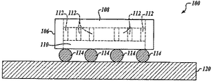
図3は、一体型3軸磁気センサ100の他の実施形態を示す。磁気センサ100はダイ106、ダイ106の第1の面に位置する第1の感知素子108、第106の第2の面に位置する第2の感知素子110を備える。感知素子108および110は、図1および2に関して説明したのと同様の、および、米国特許第7,126,330号に説明されている手法で形成される。センサ100は、第1の感知素子108をダイ106の第2の面上の導体に接続するために、ダイ106内に形成された1つまたはそれ以上のビアを有する。これは、ダイ106を回路板120に接続するバンプ114を介して、信号が、第1の感知素子108と回路板120上に位置する回路部品(図示せず)との間を通過することを可能にする。
FIG. 3 shows another embodiment of the integrated three-axis
図4に示されているように、シリコンウェハー126の第2の面上に第2の感知素子110が形成された後に、金属化(相互接続)層130が、第1の感知素子110の一部の上に形成される。それから、図2と同様に、保護層134が、金属化(相互接続)層130および第2の感知素子110の上に形成される。次に、ビア112が、任意数の所定のエッチング技術(たとえば、KOHエッチング、RIEなど)を用いて、シリコンウェハー126を第1の面から金属化(相互接続)層130までエッチングすることにより形成される。ビア112は、第1の感知素子108がウェハー126の第1の面に形成される前または後に形成されてもよい。ビアが形成された後、金属化層136を介して第1の感知素子108をウェハー126の第2の面に電気的に接続するため、金属化(相互接続)層136が所定のパターンに従って適用される。ひっかき保護層134が、補助的に、金属化(相互接続)層136および第1の感知素子108を含む第1の面の上に適用される。最後に、ダイ106を回路板120に機械的および電気的に接続するため、ひっかき保護層134が取り除かれ(たとえば、区域140)、所定位置で金属化(相互接続)層130の一部が露出される。それから、1つまたはそれ以上のバンプ114が、露出された金属化層130に結合される。これにより、回路板120上の電気部品と任意の感知素子108、110との間で、信号を伝達できるようになる。
As shown in FIG. 4, after the
図5は、本発明の他の実施形態を示しており、これは図1および3に示した実施形態の組み合わせであり、センサ180を形成している。バンプ38または114は含まれない。ダイ106は図3に示したダイに類似しており、感知素子108、110をダイの対向する面上に備え、ダイ106を通るビア112を備える。しかし、ダイ106は、直接回路板120に取り付けられており(バンプがない)、感知素子108、110は、1つまたはそれ以上の、ワイヤ40に類似するリードワイヤ140により、電気的に回路板120に取り付けられる。
FIG. 5 shows another embodiment of the present invention, which is a combination of the embodiments shown in FIGS. 1 and 3 and forms a
図6に示されているように、2つのセンサ150、152は、ダイ154の一方の面上の傾斜した面に形成または取り付けられる。あらかじめエッチングされた傾斜面は、センサ150、152が直交する場/力を計測することを可能にする。これについては、米国特許第7,126,330号により詳細に説明されている。
As shown in FIG. 6, the two
本発明の好ましい実施形態が図示および説明されたが、前述のように、多くの変更形態が、本発明の趣旨および範囲から逸脱することなく可能である。たとえば、製造工程は、異なる順序で任意に行うことができる。また、保護層のようないくつかの層は、補助的な追加とすることができる。また、センサは、電場、重力場等の他の異なるタイプの場のセンサであってもよい。センサは、場あるいは力(たとえば加速度)を計測する、異なるタイプの任意の数のセンサであってもよい。従って、本発明の範囲は、好ましい実施形態の開示に限定されない。本発明は、添付の特許請求の範囲を参照することにより完全に決定されるべきものである。 While the preferred embodiment of the invention has been illustrated and described, as noted above, many changes can be made without departing from the spirit and scope of the invention. For example, the manufacturing process can be arbitrarily performed in a different order. Also, some layers, such as protective layers, can be supplementary additions. The sensor may also be a sensor of another different type of field, such as an electric field, a gravitational field. The sensor may be any number of different types of sensors that measure a field or force (eg, acceleration). Accordingly, the scope of the invention is not limited to the disclosure of the preferred embodiment. The invention should be determined entirely by reference to the appended claims.
Claims (2)
1つまたはそれ以上の軸に沿った場を感知するための、前記第1の面上に形成された、1つまたはそれ以上の場のセンサ(34)と、
1つまたはそれ以上の軸に沿った場を感知するための、前記第2の面上に形成された、1つまたはそれ以上の場のセンサ(32)と、
前記第1の面を回路板(60)に機械的に結合し、前記第1の面上に形成された対応する1つまたはそれ以上の前記センサを、前記回路板上の部品に電気的に結合するように構成された1つまたはそれ以上の結合装置と、
前記第2の面上の対応する1つまたはそれ以上の前記センサ(32)を、前記回路板上の部品に電気的に結合するように構成された1つまたはそれ以上の装置と、
を有し、
前記第1の面上および前記第2の面上に形成される前記場のセンサは、前記第1の面および前記第2の面の面内で2つの直交する平面内の軸に沿って場を測定し、且つ、前記平面内の軸に直交する平面外の軸に沿って場を測定し、
前記平面外の軸に沿う場を測定するように構成された1つまたはそれ以上の場のセンサは、少なくとも1つの傾斜する表面上に形成され、前記傾斜する表面は、前記第1の表面および前記第2の表面の領域の両方に対して傾斜する、場の感知装置。 An integrated three-axis field sensing device on a substrate comprising substantially parallel first and second surfaces comprising:
One or more field sensors (34) formed on said first surface for sensing a field along one or more axes;
One or more field sensors (32) formed on said second surface for sensing a field along one or more axes;
The first surface is mechanically coupled to a circuit board (60), and the corresponding one or more sensors formed on the first surface are electrically coupled to components on the circuit board. One or more coupling devices configured to couple;
One or more devices configured to electrically couple corresponding one or more of the sensors (32) on the second surface to a component on the circuit board;
Have
The field sensors formed on the first surface and the second surface are fielded along axes in two orthogonal planes in the plane of the first surface and the second surface. It was measured, and the field measured along the out-of-plane axis orthogonal to the axis of said plane,
One or more field sensors configured to measure a field along the out-of-plane axis are formed on at least one inclined surface, wherein the inclined surface is the first surface and A field sensing device that is inclined with respect to both of the regions of the second surface .
Applications Claiming Priority (2)
| Application Number | Priority Date | Filing Date | Title |
|---|---|---|---|
| US11/877,537 | 2007-10-23 | ||
| US11/877,537 US7564237B2 (en) | 2007-10-23 | 2007-10-23 | Integrated 3-axis field sensor and fabrication methods |
Publications (2)
| Publication Number | Publication Date |
|---|---|
| JP2009168796A JP2009168796A (en) | 2009-07-30 |
| JP5465861B2 true JP5465861B2 (en) | 2014-04-09 |
Family
ID=40266038
Family Applications (1)
| Application Number | Title | Priority Date | Filing Date |
|---|---|---|---|
| JP2008271064A Active JP5465861B2 (en) | 2007-10-23 | 2008-10-21 | Integrated three-axis field sensor and manufacturing method thereof |
Country Status (4)
| Country | Link |
|---|---|
| US (1) | US7564237B2 (en) |
| EP (1) | EP2053415B1 (en) |
| JP (1) | JP5465861B2 (en) |
| KR (1) | KR101501929B1 (en) |
Families Citing this family (13)
| Publication number | Priority date | Publication date | Assignee | Title |
|---|---|---|---|---|
| US8390283B2 (en) | 2009-09-25 | 2013-03-05 | Everspin Technologies, Inc. | Three axis magnetic field sensor |
| US20110234218A1 (en) * | 2010-03-24 | 2011-09-29 | Matthieu Lagouge | Integrated multi-axis hybrid magnetic field sensor |
| US8518734B2 (en) * | 2010-03-31 | 2013-08-27 | Everspin Technologies, Inc. | Process integration of a single chip three axis magnetic field sensor |
| RU2470410C2 (en) * | 2010-12-28 | 2012-12-20 | Федеральное Государственное Учреждение "Научно-Производственный Комплекс "Технологический Центр" Московского Государственного Института Электронной Техники" | Method of making microsystem for detecting three magnetic induction vector components |
| CN102426344B (en) * | 2011-08-30 | 2013-08-21 | 江苏多维科技有限公司 | Triaxial magnetic field sensor |
| US20130257423A1 (en) * | 2012-04-03 | 2013-10-03 | Isentek Inc. | Hybrid magnetic sensor |
| US9658298B2 (en) | 2012-10-12 | 2017-05-23 | Memsic, Inc | Monolithic three-axis magnetic field sensor |
| KR102282640B1 (en) * | 2014-11-24 | 2021-07-27 | 주식회사 키 파운드리 | Method for manufacturing of Semiconductor Device Having a Buried Magnetic Sensor |
| RU175590U1 (en) * | 2017-04-25 | 2017-12-11 | Российская Федерация, от имени которой выступает Федеральное государственное казенное учреждение "Войсковая часть 68240" | THREE-AXIS MICROSYSTEM ANALYSIS OF WEAK MAGNETIC FIELDS |
| JP7064662B2 (en) * | 2017-04-25 | 2022-05-11 | コニカミノルタ株式会社 | Magnetic sensor |
| US11193989B2 (en) * | 2018-07-27 | 2021-12-07 | Allegro Microsystems, Llc | Magnetoresistance assembly having a TMR element disposed over or under a GMR element |
| EP3675172B8 (en) * | 2018-12-24 | 2023-10-18 | Crocus Technology Sa | Magnetic reader sensor device for reading magnetic stripes and method for manufacturing the sensor device |
| CN114114102B (en) * | 2021-11-18 | 2024-01-23 | 中国人民解放军国防科技大学 | Integrated planarization triaxial magnetic sensor and application method thereof |
Family Cites Families (16)
| Publication number | Priority date | Publication date | Assignee | Title |
|---|---|---|---|---|
| JPS6311672Y2 (en) * | 1980-12-22 | 1988-04-05 | ||
| JPS63150384U (en) * | 1987-03-24 | 1988-10-04 | ||
| JP2579995B2 (en) * | 1988-03-31 | 1997-02-12 | 株式会社東芝 | Magnetic sensor |
| US5569544A (en) | 1992-11-16 | 1996-10-29 | Nonvolatile Electronics, Incorporated | Magnetoresistive structure comprising ferromagnetic thin films and intermediate layers of less than 30 angstroms formed of alloys having immiscible components |
| JPH08167747A (en) * | 1994-12-12 | 1996-06-25 | Hitachi Cable Ltd | Hall sensor |
| FR2750769B1 (en) * | 1996-07-05 | 1998-11-13 | Thomson Csf | THIN FILM MAGNETIC FIELD SENSOR |
| US5982178A (en) | 1997-12-18 | 1999-11-09 | Honewell Inc. | Method and apparatus for sensing a desired component of an incident magnetic field using magneto resistive elements biased in different directions |
| JP2004519684A (en) * | 2001-04-09 | 2004-07-02 | コーニンクレッカ フィリップス エレクトロニクス エヌ ヴィ | Integrated circuit with power test interface |
| JP2003161770A (en) * | 2001-11-27 | 2003-06-06 | Fuji Electric Co Ltd | Magnetism detecting element |
| JP4085859B2 (en) * | 2002-03-27 | 2008-05-14 | ヤマハ株式会社 | Magnetic sensor and manufacturing method thereof |
| US7095226B2 (en) | 2003-12-04 | 2006-08-22 | Honeywell International, Inc. | Vertical die chip-on-board |
| US7271586B2 (en) | 2003-12-04 | 2007-09-18 | Honeywell International Inc. | Single package design for 3-axis magnetic sensor |
| US7126330B2 (en) | 2004-06-03 | 2006-10-24 | Honeywell International, Inc. | Integrated three-dimensional magnetic sensing device and method to fabricate an integrated three-dimensional magnetic sensing device |
| JP4453536B2 (en) * | 2004-12-10 | 2010-04-21 | トヨタ自動車株式会社 | Drive device, automobile equipped with the drive device, and control method of drive device |
| JP4613661B2 (en) * | 2005-03-29 | 2011-01-19 | ヤマハ株式会社 | Manufacturing method of 3-axis magnetic sensor |
| US7768083B2 (en) * | 2006-01-20 | 2010-08-03 | Allegro Microsystems, Inc. | Arrangements for an integrated sensor |
-
2007
- 2007-10-23 US US11/877,537 patent/US7564237B2/en active Active
-
2008
- 2008-10-16 EP EP08166849A patent/EP2053415B1/en not_active Expired - Fee Related
- 2008-10-21 JP JP2008271064A patent/JP5465861B2/en active Active
- 2008-10-22 KR KR1020080103858A patent/KR101501929B1/en active IP Right Grant
Also Published As
| Publication number | Publication date |
|---|---|
| EP2053415B1 (en) | 2011-06-29 |
| KR101501929B1 (en) | 2015-03-12 |
| JP2009168796A (en) | 2009-07-30 |
| EP2053415A3 (en) | 2010-10-06 |
| KR20090041344A (en) | 2009-04-28 |
| EP2053415A2 (en) | 2009-04-29 |
| US7564237B2 (en) | 2009-07-21 |
| US20090102475A1 (en) | 2009-04-23 |
Similar Documents
| Publication | Publication Date | Title |
|---|---|---|
| JP5465861B2 (en) | Integrated three-axis field sensor and manufacturing method thereof | |
| US7126330B2 (en) | Integrated three-dimensional magnetic sensing device and method to fabricate an integrated three-dimensional magnetic sensing device | |
| US7095226B2 (en) | Vertical die chip-on-board | |
| JP5157611B2 (en) | Magnetic sensor and manufacturing method thereof | |
| US8742520B2 (en) | Three axis magnetic sensor device and method | |
| EP2752676B1 (en) | Triaxial magnetic field sensor | |
| TWI497097B (en) | Three axis magnetic field sensor | |
| US20170108559A1 (en) | Magnetic field sensing apparatus | |
| JP2015520840A (en) | Foldable board | |
| JP2007240530A (en) | Motion sensor | |
| KR20150102052A (en) | Magnetic Sensing Apparatus, Magnetic Induction Method and Preparation Technique Therefor | |
| US8459112B2 (en) | Systems and methods for three dimensional sensors | |
| JP2007506274A (en) | Method for manufacturing electronic device and electronic device | |
| CN111044951B (en) | Three-axis magnetic field sensor and manufacturing method thereof | |
| RU2470410C2 (en) | Method of making microsystem for detecting three magnetic induction vector components |
Legal Events
| Date | Code | Title | Description |
|---|---|---|---|
| A621 | Written request for application examination |
Free format text: JAPANESE INTERMEDIATE CODE: A621 Effective date: 20111021 |
|
| A131 | Notification of reasons for refusal |
Free format text: JAPANESE INTERMEDIATE CODE: A131 Effective date: 20120621 |
|
| A521 | Request for written amendment filed |
Free format text: JAPANESE INTERMEDIATE CODE: A523 Effective date: 20120827 |
|
| A131 | Notification of reasons for refusal |
Free format text: JAPANESE INTERMEDIATE CODE: A131 Effective date: 20130109 |
|
| A131 | Notification of reasons for refusal |
Free format text: JAPANESE INTERMEDIATE CODE: A131 Effective date: 20130819 |
|
| A601 | Written request for extension of time |
Free format text: JAPANESE INTERMEDIATE CODE: A601 Effective date: 20131118 |
|
| A521 | Request for written amendment filed |
Free format text: JAPANESE INTERMEDIATE CODE: A523 Effective date: 20131119 |
|
| A602 | Written permission of extension of time |
Free format text: JAPANESE INTERMEDIATE CODE: A602 Effective date: 20131121 |
|
| TRDD | Decision of grant or rejection written | ||
| A01 | Written decision to grant a patent or to grant a registration (utility model) |
Free format text: JAPANESE INTERMEDIATE CODE: A01 Effective date: 20131225 |
|
| A61 | First payment of annual fees (during grant procedure) |
Free format text: JAPANESE INTERMEDIATE CODE: A61 Effective date: 20140123 |
|
| R150 | Certificate of patent or registration of utility model |
Free format text: JAPANESE INTERMEDIATE CODE: R150 Ref document number: 5465861 Country of ref document: JP Free format text: JAPANESE INTERMEDIATE CODE: R150 |
|
| R250 | Receipt of annual fees |
Free format text: JAPANESE INTERMEDIATE CODE: R250 |
|
| R250 | Receipt of annual fees |
Free format text: JAPANESE INTERMEDIATE CODE: R250 |
|
| R250 | Receipt of annual fees |
Free format text: JAPANESE INTERMEDIATE CODE: R250 |
|
| R250 | Receipt of annual fees |
Free format text: JAPANESE INTERMEDIATE CODE: R250 |
|
| R250 | Receipt of annual fees |
Free format text: JAPANESE INTERMEDIATE CODE: R250 |
|
| R250 | Receipt of annual fees |
Free format text: JAPANESE INTERMEDIATE CODE: R250 |
|
| R250 | Receipt of annual fees |
Free format text: JAPANESE INTERMEDIATE CODE: R250 |
|
| R250 | Receipt of annual fees |
Free format text: JAPANESE INTERMEDIATE CODE: R250 |