JP5462524B2 - Semiconductor device - Google Patents

Semiconductor device Download PDF

Info

Publication number
JP5462524B2
JP5462524B2 JP2009116316A JP2009116316A JP5462524B2 JP 5462524 B2 JP5462524 B2 JP 5462524B2 JP 2009116316 A JP2009116316 A JP 2009116316A JP 2009116316 A JP2009116316 A JP 2009116316A JP 5462524 B2 JP5462524 B2 JP 5462524B2
Authority
JP
Japan
Prior art keywords
electrode
layer
semiconductor device
via hole
silicide
Prior art date
Legal status (The legal status is an assumption and is not a legal conclusion. Google has not performed a legal analysis and makes no representation as to the accuracy of the status listed.)
Expired - Fee Related
Application number
JP2009116316A
Other languages
Japanese (ja)
Other versions
JP2010267695A (en
JP2010267695A5 (en
Inventor
太志郎 斉藤
隆行 甲斐
崇文 大熊
斉 山西
Current Assignee (The listed assignees may be inaccurate. Google has not performed a legal analysis and makes no representation or warranty as to the accuracy of the list.)
Panasonic Corp
Panasonic Holdings Corp
Original Assignee
Panasonic Corp
Matsushita Electric Industrial Co Ltd
Priority date (The priority date is an assumption and is not a legal conclusion. Google has not performed a legal analysis and makes no representation as to the accuracy of the date listed.)
Filing date
Publication date
Application filed by Panasonic Corp, Matsushita Electric Industrial Co Ltd filed Critical Panasonic Corp
Priority to JP2009116316A priority Critical patent/JP5462524B2/en
Publication of JP2010267695A publication Critical patent/JP2010267695A/en
Publication of JP2010267695A5 publication Critical patent/JP2010267695A5/ja
Application granted granted Critical
Publication of JP5462524B2 publication Critical patent/JP5462524B2/en
Expired - Fee Related legal-status Critical Current
Anticipated expiration legal-status Critical

Links

Images

Description

本発明は、半導体基板に貫通電極層が形成された半導体装置に関するものである。   The present invention relates to a semiconductor device in which a through electrode layer is formed on a semiconductor substrate.

近年、電子機器に使用される集積回路において、パッケージ(半導体装置)の小型化が求められている。小型化の一例として、集積回路のパッケージ面積の低減を目的として、従来のワイヤーボンディングに代わって、半導体装置の半導体基板を貫通する貫通電極が用いられている。   In recent years, miniaturization of packages (semiconductor devices) has been required in integrated circuits used in electronic devices. As an example of downsizing, for the purpose of reducing the package area of an integrated circuit, a through electrode penetrating a semiconductor substrate of a semiconductor device is used instead of conventional wire bonding.

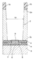
図9は、従来の半導体装置の一例を示す部分断面図である。   FIG. 9 is a partial cross-sectional view showing an example of a conventional semiconductor device.

図9において、半導体装置101は、シリコンなどの半導体基板102と、半導体基板102の裏面102bからパッド電極105に到達するビアホール107と、ビアホール107の側壁107a及び半導体基板102の裏面102bに形成された第2酸化膜109と、ビアホール107の内部及び半導体基板102の裏面102bに形成されたバリア層110及び再配線層111とから概略構成されている。   In FIG. 9, the semiconductor device 101 is formed in a semiconductor substrate 102 such as silicon, a via hole 107 reaching the pad electrode 105 from the back surface 102 b of the semiconductor substrate 102, a side wall 107 a of the via hole 107, and a back surface 102 b of the semiconductor substrate 102. The second oxide film 109 is roughly constituted by a barrier layer 110 and a rewiring layer 111 formed in the via hole 107 and on the back surface 102b of the semiconductor substrate 102.

図10は、従来の半導体装置の製造方法を示すフローチャートであり、図11A〜図12Dは、従来の半導体装置の製造方法を説明するための部分断面図である。   FIG. 10 is a flowchart showing a conventional method for manufacturing a semiconductor device, and FIGS. 11A to 12D are partial cross-sectional views for explaining a conventional method for manufacturing a semiconductor device.

最初に、図11Aに示すように、不図示の電子回路が形成された半導体基板102の表面102aの上の第1酸化膜106の上にパッド電極105及びパッシベーション膜104が形成された後、パッシベーション膜104の上に、不図示の接着剤を介して、支持基板103が接着される(図10のステップS101参照)。   First, as shown in FIG. 11A, after the pad electrode 105 and the passivation film 104 are formed on the first oxide film 106 on the surface 102a of the semiconductor substrate 102 on which an electronic circuit (not shown) is formed, the passivation is performed. The support substrate 103 is bonded onto the film 104 via an adhesive (not shown) (see step S101 in FIG. 10).

次に、図11Bに示すように、半導体基板102の裏面102bの上に、パッド電極105に相当する位置を開口するために、レジスト112が形成される(図10のステップS102参照)。   Next, as shown in FIG. 11B, a resist 112 is formed on the back surface 102b of the semiconductor substrate 102 in order to open a position corresponding to the pad electrode 105 (see step S102 in FIG. 10).

そして、図11Cに示すように、レジスト112をマスクとして、半導体基板102をエッチングすることにより、第1酸化膜106に到達するビアホール107が形成される(図10のステップS103参照)。   Then, as shown in FIG. 11C, the via hole 107 reaching the first oxide film 106 is formed by etching the semiconductor substrate 102 using the resist 112 as a mask (see step S103 in FIG. 10).

続いて、図11Dに示すように、レジスト112をマスクとして、第1酸化膜106をエッチングすることにより、パッド電極105に到達するビアホール107が形成される(図10のステップS104参照)。   Subsequently, as shown in FIG. 11D, the first oxide film 106 is etched using the resist 112 as a mask, thereby forming a via hole 107 reaching the pad electrode 105 (see step S104 in FIG. 10).

次に、図12Aに示すように、レジスト112を半導体基板102の裏面102bから除去する(図10のステップS105参照)。   Next, as shown in FIG. 12A, the resist 112 is removed from the back surface 102b of the semiconductor substrate 102 (see step S105 in FIG. 10).

そして、図12Bに示すように、ビアホール107の側壁107a及び半導体基板102の裏面102bに第2酸化膜109をそれぞれ形成する(図10のステップS106参照)。   Then, as shown in FIG. 12B, a second oxide film 109 is formed on the side wall 107a of the via hole 107 and the back surface 102b of the semiconductor substrate 102 (see step S106 in FIG. 10).

次に、図12Cに示すように、ビアホール107の底部の第2酸化膜109をエッチングすることにより、パッド電極105を再度露出させる(図10のステップS107参照)。   Next, as shown in FIG. 12C, the pad electrode 105 is exposed again by etching the second oxide film 109 at the bottom of the via hole 107 (see step S107 in FIG. 10).

続いて、図12Dに示すように、バリア層110及び再配線層111を第2酸化膜109上に順に形成する(図10のステップS108参照)。   Subsequently, as shown in FIG. 12D, a barrier layer 110 and a redistribution layer 111 are sequentially formed on the second oxide film 109 (see step S108 in FIG. 10).

パッド電極105は、バリア層110及び再配線層111で構成される貫通電極108を通して、半導体基板102の裏面102bへ電気的に接続されている。   The pad electrode 105 is electrically connected to the back surface 102 b of the semiconductor substrate 102 through the through electrode 108 constituted by the barrier layer 110 and the rewiring layer 111.

パッド電極105と貫通電極108は、ビアホール107の内径に応じた面積で接触しており、パッド電極105と貫通電極108の間の抵抗値は、この接触面積によって決定される。   The pad electrode 105 and the through electrode 108 are in contact with each other in an area corresponding to the inner diameter of the via hole 107, and the resistance value between the pad electrode 105 and the through electrode 108 is determined by this contact area.

特開2005−235860号公報JP 2005-235860 A

しかしながら、前記従来の構成では、パッド電極105と貫通電極108の間の抵抗値はビアホール107の内径の寸法に依存するため、その抵抗値は、ビアホール107の内径の寸法のばらつきにより変動するという課題を有している。   However, in the conventional configuration, since the resistance value between the pad electrode 105 and the through electrode 108 depends on the inner diameter of the via hole 107, the resistance value varies due to variations in the inner diameter of the via hole 107. have.

本発明は、前記従来の課題を解決するもので、パッド電極と貫通電極との間の抵抗値がビアホールの内径の寸法のばらつきに依存しない、信頼性に優れた半導体装置を提供することを目的とする。   The present invention solves the above-described conventional problems, and an object of the present invention is to provide a highly reliable semiconductor device in which the resistance value between the pad electrode and the through electrode does not depend on the variation in the inner diameter of the via hole. And

上記目的を達成するために、本発明は以下のように構成する。   In order to achieve the above object, the present invention is configured as follows.

本発明の第1態様によれば、半導体基板の表面に形成された第1絶縁膜と、
前記第1絶縁膜の中に形成され、かつ、外部接続端子を有する電極部と、
前記半導体基板の裏面から前記表面に貫通するビアホールと、
前記ビアホールの側壁及び前記半導体基板の前記裏面に形成された第2絶縁膜と、
前記ビアホールの前記側壁上の前記第2絶縁膜と前記半導体基板の前記裏面上の前記第2絶縁膜と前記ビアホールの底面の前記第1絶縁膜とに形成された貫通電極層と、
前記電極部と前記貫通電極層との間に形成され、かつ前記電極部及び前記貫通電極層に接続されたシリサイド層と、
を備え、
前記ビアホールの中心軸を含む平面で切断された断面における、前記シリサイド層の幅Aと前記ビアホールの底部の幅Bとの関係が、A≦Bであることを特徴とする半導体装置を提供する。
According to the first aspect of the present invention, the first insulating film formed on the surface of the semiconductor substrate;
An electrode portion formed in the first insulating film and having an external connection terminal;
A via hole penetrating from the back surface of the semiconductor substrate to the front surface;
A second insulating film formed on a sidewall of the via hole and the back surface of the semiconductor substrate;
A through electrode layer formed on the second insulating film on the sidewall of the via hole, the second insulating film on the back surface of the semiconductor substrate, and the first insulating film on the bottom surface of the via hole;
A silicide layer formed between the electrode portion and the through electrode layer and connected to the electrode portion and the through electrode layer;
With
The semiconductor device is characterized in that the relation between the width A of the silicide layer and the width B of the bottom of the via hole in a cross section cut along a plane including the central axis of the via hole is A ≦ B.

本発明の第2態様によれば、前記シリサイド層と前記電極部とは、コンタクト電極を介して接続されたことを特徴とする第1の態様に記載の半導体装置を提供する。 According to a second aspect of the present invention, there is provided the semiconductor device according to the first aspect, wherein the silicide layer and the electrode portion are connected via a contact electrode .

本発明の第3態様によれば、前記ビアホールの前記中心軸を含む前記平面において、前記シリサイド層の前記幅と前記コンタクト電極の幅が等しいことを特徴とする第2の態様に記載の半導体装置を提供する。 According to a third aspect of the present invention, in the semiconductor device according to the second aspect, the width of the silicide layer and the width of the contact electrode are equal in the plane including the central axis of the via hole. I will provide a.

本発明の第4態様によれば、前記ビアホールの前記中心軸を含む前記平面において、前記ビアホールの前記底部の前記幅より前記電極部の幅が大きいことを特徴とする第1〜3のいずれか1つの態様に記載の半導体装置を提供する。 According to a fourth aspect of the present invention, in any one of the first to third aspects, in the plane including the central axis of the via hole, the width of the electrode portion is larger than the width of the bottom portion of the via hole . A semiconductor device according to one aspect is provided.

本発明の第5態様によれば、前記電極部は、
前記電極部の本体部と、
前記電極部の前記本体部と前記第1絶縁膜との間に配置された第1バリア層とを備えることを特徴とする第1〜4のいずれか1つの態様に記載の半導体装置を提供する。
According to a fifth aspect of the present invention, the electrode portion is
A body portion of the electrode portion;
The semiconductor device according to any one of the first to fourth aspects, further comprising a first barrier layer disposed between the main body portion of the electrode portion and the first insulating film. .

本発明の第6態様によれば、前記電極部は、
前記電極部の本体部と、
前記電極部の前記本体部と前記第1絶縁膜との間に配置されかつ前記シリサイド層に接触する第1バリア層と、
前記第1絶縁膜の外面側でかつ前記電極部の前記本体部の外面に配置されて前記外部接続端子として機能するパッド電極部とを備えることを特徴とする第1〜4のいずれか1つの態様に記載の半導体装置を提供する。
According to a sixth aspect of the present invention, the electrode portion is
A body portion of the electrode portion;
A first barrier layer disposed between the main body portion of the electrode portion and the first insulating film and in contact with the silicide layer;
One of the first to fourth aspects, further comprising: a pad electrode portion that is disposed on the outer surface side of the first insulating film and on the outer surface of the main body portion of the electrode portion and functions as the external connection terminal. to provide a semiconductor device mounting serial to embodiment.

本発明の第7態様によれば、前記シリサイド層は、前記半導体基板、ポリシリコン膜、又はアモルファスシリコン膜のいずれかに形成されることを特徴とする
第1〜6のいずれか1つの態様に記載の半導体装置を提供する。
According to a seventh aspect of the present invention, the silicide layer is formed on any one of the semiconductor substrate, a polysilicon film, or an amorphous silicon film.
To provide a semiconductor device mounting serial to a sixth one of the aspects.

本発明の第8態様によれば、前記シリサイド層は、タングステンシリサイド、チタンシリサイド、コバルトシリサイド、又は、ニッケルシリサイドのいずれかからから成ることを特徴とする
第1〜7のいずれか1つの態様に記載の半導体装置を提供する。
According to an eighth aspect of the present invention, the silicide layer is made of any of tungsten silicide, titanium silicide, cobalt silicide, or nickel silicide.
To provide a semiconductor device mounting serial to first to seventh any one aspect.

本発明の第9態様によれば、前記電極部の本体部は、タングステン、アルミニウム、又はその合金、銅のいずれかからから成ることを特徴とする
第7又は8の態様に記載の半導体装置を提供する。
According to a ninth aspect of the present invention, the main body portion of the electrode portion is made of tungsten, aluminum, an alloy thereof, or copper.
Providing a semiconductor device mounting serial to aspects of the seventh or eighth.

本発明の第10態様によれば、前記第1バリア層は、チタン、チタンナイトライド、チタンタングステン、タンタル、タンタルナイトライド、又は、高融点金属の積層膜から成ることを特徴とする
第6の態様に記載の半導体装置を提供する。
本発明の第11態様によれば、前記貫通電極層は、
前記ビアホールの前記側壁上の前記第2絶縁膜と前記半導体基板の前記裏面上の前記第2絶縁膜と前記ビアホールの底面の前記第1絶縁膜とに形成された第2バリア層と、
前記第2バリア層上に形成された再配線層とを備え、
前記第2バリア層は、チタン、チタンナイトライド、チタンタングステン、タンタル、タンタルナイトライド、又は、高融点金属の積層膜から成ることを特徴とする
第1〜10のいずれか1つの態様に記載の半導体装置を提供する。
本発明の第12態様によれば、前記電極部が、単一のコンタクト電極部材又は複数のコンタクト電極部材で構成されていることを特徴とする
第1〜11のいずれか1つの態様に記載の半導体装置を提供する。
本発明の第13態様によれば、前記パッド電極は、アルミニウム、銅又はその合金と、チタン、チタンナイトライド、タンタル、タンタルナイトライド、高融点金属、又は、その化合物のいずれかからから成ることを特徴とする
第6の態様に記載の半導体装置を提供する。
According to a tenth aspect of the present invention, the first barrier layer is composed of a laminated film of titanium, titanium nitride, titanium tungsten, tantalum, tantalum nitride, or a refractory metal.
To provide a semiconductor device mounting serial to a sixth aspect of.
According to an eleventh aspect of the present invention, the through electrode layer comprises:
A second barrier layer formed on the second insulating film on the side wall of the via hole, the second insulating film on the back surface of the semiconductor substrate, and the first insulating film on the bottom surface of the via hole;
A rewiring layer formed on the second barrier layer,
The second barrier layer is composed of titanium, titanium nitride, titanium tungsten, tantalum, tantalum nitride, or a laminated film of a refractory metal.
A semiconductor device according to any one of the first to tenth aspects is provided.
According to a twelfth aspect of the present invention, the electrode portion is composed of a single contact electrode member or a plurality of contact electrode members.
A semiconductor device according to any one of the first to eleventh aspects is provided.
According to the thirteenth aspect of the present invention, the pad electrode is composed of aluminum, copper, or an alloy thereof, and any of titanium, titanium nitride, tantalum, tantalum nitride, a refractory metal, or a compound thereof. Characterized by
A semiconductor device according to a sixth aspect is provided.

以上のように、本発明の半導体装置によれば、パッド電極を含む電極部と貫通電極層との間の抵抗値は、前記電極部及び前記貫通電極層に接続されたシリサイド層の幅(例えば、シリサイド層が円形の場合の直径)寸法に依存し、ビアホールの幅(例えば、ビアホールが円形の場合の内径)寸法のばらつきに依存しないため、抵抗値ばらつきに依存しない信頼性に優れた半導体装置を提供することができる。   As described above, according to the semiconductor device of the present invention, the resistance value between the electrode portion including the pad electrode and the through electrode layer has the width of the silicide layer connected to the electrode portion and the through electrode layer (for example, Depends on the dimension of the diameter when the silicide layer is circular) and does not depend on the variation of the width of the via hole (for example, the inner diameter when the via hole is circular). Can be provided.

また、ビアホールの幅(例えば、ビアホールが円形の場合の内径)寸法は電極部のパッド電極の幅(例えば、パッド電極が円形の場合の直径)寸法よりも大きくすることが可能であるため、ビアホールのアスペクト比を低減することもできる。   Also, the width of the via hole (for example, the inner diameter when the via hole is circular) can be made larger than the width of the pad electrode (for example, the diameter when the pad electrode is circular) of the electrode portion. It is also possible to reduce the aspect ratio.

さらに、ビアホールの幅(例えば、ビアホールが円形の場合の内径)寸法は、電極部のパッド電極の幅(例えば、パッド電極が円形の場合の直径)寸法よりも大きくすることが可能であるため、電極部のパッド電極の大きさを縮小することにより、半導体装置の一例としての半導体チップの面積を削減することもできる。   Furthermore, the width of the via hole (for example, the inner diameter when the via hole is circular) can be made larger than the width of the pad electrode of the electrode portion (for example, the diameter when the pad electrode is circular). By reducing the size of the pad electrode in the electrode portion, the area of a semiconductor chip as an example of a semiconductor device can be reduced.

本発明の実施の形態1における半導体装置の部分断面図Partial sectional view of the semiconductor device in the first embodiment of the present invention 本発明の実施の形態1における半導体装置の製造方法を示すフローチャートFlowchart showing a method for manufacturing a semiconductor device in the first embodiment of the present invention. 本発明の実施の形態1における半導体装置の製造方法の工程を示す部分断面図The fragmentary sectional view which shows the process of the manufacturing method of the semiconductor device in Embodiment 1 of this invention 図3Aに続く、本発明の実施の形態1における半導体装置の製造方法の工程を示す部分断面図FIG. 3A is a partial cross-sectional view showing the steps of the method for manufacturing the semiconductor device in the first embodiment of the present invention, following FIG. 3A. 図3Bに続く、本発明の実施の形態1における半導体装置の製造方法の工程を示す部分断面図3B is a partial cross-sectional view showing the process of the method for manufacturing the semiconductor device in the first embodiment of the present invention, following FIG. 3B. 図3Cに続く、本発明の実施の形態1における半導体装置の製造方法の工程を示す部分断面図FIG. 3C is a partial cross-sectional view showing the process of the method for manufacturing the semiconductor device in the first embodiment of the present invention, following FIG. 3C. 図3Dに続く、本発明の実施の形態1における半導体装置の製造方法の工程を示す部分断面図3D is a partial cross-sectional view showing the process of the method for manufacturing the semiconductor device in the first embodiment of the present invention, following FIG. 3D. 図4Aに続く、本発明の実施の形態1における半導体装置の製造方法の工程を示す部分断面図4A is a partial cross-sectional view showing the process of the method for manufacturing the semiconductor device in the first embodiment of the present invention, following FIG. 4A. 図4Bに続く、本発明の実施の形態1における半導体装置の製造方法の工程を示す部分断面図4B is a partial cross-sectional view showing the process of the method for manufacturing the semiconductor device in the first embodiment of the present invention, following FIG. 4B. 本発明の実施の形態1の変形例1における半導体装置を示す部分断面図The fragmentary sectional view which shows the semiconductor device in the modification 1 of Embodiment 1 of this invention 本発明の実施の形態1の変形例2における半導体装置を示す部分断面図The fragmentary sectional view which shows the semiconductor device in the modification 2 of Embodiment 1 of this invention 本発明の実施の形態1の変形例3における半導体装置を示す部分断面図The fragmentary sectional view which shows the semiconductor device in the modification 3 of Embodiment 1 of this invention 本発明の実施の形態2における半導体装置の部分断面図Sectional drawing of the semiconductor device in Embodiment 2 of this invention 本発明の実施の形態2における半導体装置の製造方法を示すフローチャートThe flowchart which shows the manufacturing method of the semiconductor device in Embodiment 2 of this invention. 本発明の実施の形態2における半導体装置の製造方法を示す部分断面図Sectional drawing which shows the manufacturing method of the semiconductor device in Embodiment 2 of this invention 図7Aに続く、本発明の実施の形態2における半導体装置の製造方法を示す部分断面図7A is a partial cross-sectional view showing the method for manufacturing the semiconductor device in the second embodiment of the present invention, following FIG. 7A. 図7Bに続く、本発明の実施の形態2における半導体装置の製造方法を示す部分断面図7B is a partial cross-sectional view showing the method for manufacturing the semiconductor device in the second embodiment of the present invention, following FIG. 7B. 図7Cに続く、本発明の実施の形態2における半導体装置の製造方法を示す部分断面図7C is a partial cross-sectional view showing the method for manufacturing the semiconductor device in the second embodiment of the present invention, following FIG. 7C. 図7Dに続く、本発明の実施の形態2における半導体装置の製造方法を示す部分断面図7D is a partial cross-sectional view showing the method for manufacturing the semiconductor device in the second embodiment of the present invention, following FIG. 7D. 図8Aに続く、本発明の実施の形態2における半導体装置の製造方法を示す部分断面図8A is a partial cross-sectional view showing the method for manufacturing the semiconductor device in the second embodiment of the present invention, following FIG. 8A. 図8Bに続く、本発明の実施の形態2における半導体装置の製造方法を示す部分断面図8B is a partial cross-sectional view showing the method for manufacturing the semiconductor device in the second embodiment of the present invention, following FIG. 8B. 本発明の実施の形態2の変形例1における半導体装置を示す部分断面図The fragmentary sectional view which shows the semiconductor device in the modification 1 of Embodiment 2 of this invention 本発明の実施の形態2の変形例2における半導体装置を示す部分断面図The fragmentary sectional view which shows the semiconductor device in the modification 2 of Embodiment 2 of this invention 本発明の実施の形態2の変形例3における半導体装置を示す部分断面図The fragmentary sectional view which shows the semiconductor device in the modification 3 of Embodiment 2 of this invention 従来の半導体装置の部分断面図Partial sectional view of a conventional semiconductor device 従来の半導体装置の製造方法を示すフローチャートA flowchart showing a conventional method of manufacturing a semiconductor device 従来の半導体装置の製造方法の工程を示す部分断面図Sectional drawing which shows the process of the manufacturing method of the conventional semiconductor device 図11Aに続く、従来の半導体装置の製造方法の工程を示す部分断面図FIG. 11A is a partial cross-sectional view showing the steps of the conventional method for manufacturing a semiconductor device, following FIG. 図11Bに続く、従来の半導体装置の製造方法の工程を示す部分断面図FIG. 11B is a partial cross-sectional view showing the steps of the conventional method for manufacturing the semiconductor device, following FIG. 図11Cに続く、従来の半導体装置の製造方法の工程を示す部分断面図FIG. 11C is a partial cross-sectional view showing the process of the conventional method for manufacturing a semiconductor device, following FIG. 11C 図11Dに続く、従来の半導体装置の製造方法の工程を示す部分断面図FIG. 11D is a partial cross-sectional view showing a process of the conventional semiconductor device manufacturing method following FIG. 11D 図12Aに続く、従来の半導体装置の製造方法の工程を示す部分断面図FIG. 12A is a partial cross-sectional view showing a process of the conventional semiconductor device manufacturing method following FIG. 図12Bに続く、従来の半導体装置の製造方法の工程を示す部分断面図FIG. 12B is a partial cross-sectional view showing the steps of the conventional method for manufacturing the semiconductor device, following FIG. 図12Cに続く、従来の半導体装置の製造方法の工程を示す部分断面図FIG. 12C is a partial cross-sectional view showing the steps of the conventional method for manufacturing the semiconductor device, following FIG. 本発明の実施の形態1の半導体装置において、コンタクト電極形成前にシリサイドを形成する場合に、コンタクト電極が複数のコンタクト電極部材である例を示す部分断面図The semiconductor device of Embodiment 1 of this invention WHEREIN: When forming a silicide before contact electrode formation, the fragmentary sectional view which shows the example whose contact electrode is a several contact electrode member 本発明の実施の形態1の半導体装置において、コンタクト電極形成後にシリサイドを形成する場合に、コンタクト電極が複数のコンタクト電極部材である例を示す部分断面図The semiconductor device of Embodiment 1 of this invention WHEREIN: When forming a silicide after contact electrode formation, the fragmentary sectional view which shows the example whose contact electrode is a several contact electrode member 本発明の実施の形態2の半導体装置において、コンタクト電極形成前にシリサイドを形成する場合に、コンタクト電極が複数のコンタクト電極部材である例を示す部分断面図The semiconductor device of Embodiment 2 of this invention WHEREIN: When forming silicide before contact electrode formation, the fragmentary sectional view which shows the example whose contact electrode is a several contact electrode member 本発明の実施の形態2の半導体装置において、コンタクト電極形成後にシリサイドを形成する場合に、コンタクト電極が複数のコンタクト電極部材である例を示す部分断面図In the semiconductor device of Embodiment 2 of this invention, when forming a silicide after contact electrode formation, the fragmentary sectional view which shows the example whose contact electrode is a several contact electrode member

以下、本発明の実施の形態について、図面を参照しながら説明する。以下の説明において、同じ構成には同じ符号を付して説明を省略している。   Hereinafter, embodiments of the present invention will be described with reference to the drawings. In the following description, the same components are denoted by the same reference numerals and description thereof is omitted.

(実施の形態1)
図1は、本発明の実施の形態1における半導体装置の部分断面図である。
(Embodiment 1)
FIG. 1 is a partial cross-sectional view of the semiconductor device according to the first embodiment of the present invention.

図1において、半導体装置1は、半導体基板2と、第1酸化膜8と、電極部18(パッド電極5と、コンタクト電極6と、第1バリア層7)と、シリサイド層9と、ビアホール10と、第2酸化膜12と、貫通電極層11(第2バリア層13と再配線層14)と、支持基板3と、絶縁膜の一例であるパッシベーション膜4とで構成されている。   In FIG. 1, the semiconductor device 1 includes a semiconductor substrate 2, a first oxide film 8, an electrode portion 18 (pad electrode 5, contact electrode 6, first barrier layer 7), silicide layer 9, and via hole 10. And the second oxide film 12, the through electrode layer 11 (the second barrier layer 13 and the rewiring layer 14), the support substrate 3, and the passivation film 4 which is an example of an insulating film.

第1酸化膜8は、例えばSiOなどで構成され、絶縁膜の一例として、半導体基板2の表面(図1では下面)2aに形成されて、半導体基板2とパッド電極5とを絶縁する機能を有している。 The first oxide film 8 is made of, for example, SiO 2 and is formed on the surface (lower surface in FIG. 1) 2a of the semiconductor substrate 2 as an example of an insulating film, and insulates the semiconductor substrate 2 and the pad electrode 5 from each other. have.

パッド電極5は、電極部の外部接続端子の一例として機能し、後述する導電性材料で構成され、第1酸化膜8の表面に、第1酸化膜8の表面から突出して形成されている。   The pad electrode 5 functions as an example of an external connection terminal of the electrode portion, is made of a conductive material described later, and is formed on the surface of the first oxide film 8 so as to protrude from the surface of the first oxide film 8.

コンタクト電極6は、電極部の本体部の一例として機能し、後述する導電性材料で構成され、第1酸化膜8の内部に形成され、かつ外面がパッド電極5に接触してパッド電極5と接続されている。図1では、コンタクト電極6は、パッド電極5よりも幅が小さく形成されている。   The contact electrode 6 functions as an example of a main body portion of the electrode portion, is made of a conductive material, which will be described later, is formed inside the first oxide film 8, and the outer surface is in contact with the pad electrode 5 to contact the pad electrode 5. It is connected. In FIG. 1, the contact electrode 6 is formed to have a smaller width than the pad electrode 5.

第1バリア層7は、電極部の一部を構成し、後述する導電性材料で構成され、パッド電極5と接続された外面を除くコンタクト電極6の他の面(側面及び内面)をすべて覆うように形成されて、第1酸化膜8とコンタクト電極6との密着性を高める機能を有している。なお、この第1バリア層7は、パッド電極5と接続された外面に形成されていても良い。   The first barrier layer 7 constitutes a part of the electrode portion, is made of a conductive material described later, and covers all other surfaces (side surfaces and inner surfaces) of the contact electrode 6 except for the outer surface connected to the pad electrode 5. Thus, the first oxide film 8 and the contact electrode 6 have a function of improving the adhesion. The first barrier layer 7 may be formed on the outer surface connected to the pad electrode 5.

シリサイド層9は、後述するように金属とシリコンの合金で構成された導電性材料を有し、かつ、コンタクト電極6の内面側に、第1バリア層7を介して配置される。このシリサイド層9は、コンタクト電極6と貫通電極層11との間の低抵抗を目的とするものである。すなわち、コンタクト電極6上の第1バリア層7と後述する貫通電極層11との間に形成されて、貫通電極層11及び第1バリア層7に接続されるように形成されている。このシリサイド層9を配置した目的は、パッド電極5と貫通電極層11との間の抵抗値が、ビアホール10の内径に依存しないようにすることである。そのため、シリサイド層9の材料は、低抵抗を目的にTiSiなどを用いる。 The silicide layer 9 has a conductive material composed of an alloy of metal and silicon as will be described later, and is disposed on the inner surface side of the contact electrode 6 via the first barrier layer 7. The silicide layer 9 is intended for low resistance between the contact electrode 6 and the through electrode layer 11. That is, it is formed between the first barrier layer 7 on the contact electrode 6 and a through electrode layer 11 described later, and is formed so as to be connected to the through electrode layer 11 and the first barrier layer 7. The purpose of disposing the silicide layer 9 is to prevent the resistance value between the pad electrode 5 and the through electrode layer 11 from depending on the inner diameter of the via hole 10. Therefore, the material of the silicide layer 9 is TiSi 2 or the like for the purpose of low resistance.

本実施の形態でのシリサイド層9は、ビアホール10内に向けて(表面2aよりも上向きに)、ビアホール10の底面より少し突出して形成されているが、Siと相互拡散せずにシリサイドを形成する材料の場合は、必ずしも突出する必要はない。   The silicide layer 9 in the present embodiment is formed slightly protruding from the bottom surface of the via hole 10 toward the inside of the via hole 10 (upward from the surface 2a), but forms silicide without interdiffusing with Si. In the case of the material to be used, it is not always necessary to protrude.

ビアホール10は、半導体基板2の裏面(図1の紙面上面)2bから表面(図1の紙面下面)2aまで、すなわち、シリサイド層9及び第1酸化膜8に到達するように、半導体基板2を貫通して、形成されている。ビアホール10は、図1に示すように、裏面2bから表面2aに向かうに従い内径が徐々に小さくなるように側壁10aが傾斜した、やや先すぼまりの円錐面形状を側壁10aが有するように形成されている。   The via hole 10 extends from the back surface (upper surface in FIG. 1) 2b of the semiconductor substrate 2 to the front surface (lower surface in FIG. 1) 2a, that is, to reach the silicide layer 9 and the first oxide film 8. It penetrates and is formed. As shown in FIG. 1, the via hole 10 is formed so that the side wall 10a has a conical surface shape with a slightly tapered shape in which the side wall 10a is inclined so that the inner diameter gradually decreases from the back surface 2b toward the front surface 2a. Has been.

第2酸化膜12は、例えばSiOなどで構成され、絶縁膜の一例として、ビアホール10の側壁10aの全面及び半導体基板2の裏面2bに形成されて、貫通電極層11と半導体基板2とを絶縁する機能を有している。 The second oxide film 12 is made of, for example, SiO 2 and is formed on the entire side wall 10a of the via hole 10 and the back surface 2b of the semiconductor substrate 2 as an example of an insulating film. Has the function of insulation.

貫通電極層11は、第2バリア層13と再配線層14とで構成されている。   The through electrode layer 11 includes a second barrier layer 13 and a rewiring layer 14.

第2バリア層13は、第2酸化膜12と再配線層14との密着性を高めるためのものであり、後述するような材料で構成され、ビアホール10の底面(すなわち、半導体基板2の表面2aとシリサイド層9)上とビアホール10の側壁10aの第2酸化膜12の上と半導体基板2の裏面2bの第2酸化膜12の上とに一体的に形成され、かつビアホール10の底面でシリサイド層9と接続されている。シリサイド層9と接続する部分では、シリサイド層9がビアホール10の底面より少し突出している分だけ、ビアホール10の底面より少し盛り上がった状態で、第2バリア層13が形成されている。   The second barrier layer 13 is for enhancing the adhesion between the second oxide film 12 and the redistribution layer 14 and is made of a material as described later, and is the bottom surface of the via hole 10 (that is, the surface of the semiconductor substrate 2). 2a and the silicide layer 9), on the second oxide film 12 on the side wall 10a of the via hole 10 and on the second oxide film 12 on the back surface 2b of the semiconductor substrate 2, and on the bottom surface of the via hole 10 It is connected to the silicide layer 9. In the portion connected to the silicide layer 9, the second barrier layer 13 is formed in a state where the silicide layer 9 slightly protrudes from the bottom surface of the via hole 10 by the amount that the silicide layer 9 protrudes slightly from the bottom surface of the via hole 10.

再配線層14は、第2バリア層13の上に形成されている。すなわち、ビアホール10の底面上の第2バリア層13と、ビアホール10の側壁10aの第2酸化膜12の上の第2バリア層13と、半導体基板2の裏面2bの第2酸化膜12の上の第2バリア層13とにそれぞれ一体的に再配線層14が形成されている。この再配線層14は、パッド電極5(基板表面)から、基板裏面への電気配線を目的として形成されるものであり、例えばCuなどから構成される。   The rewiring layer 14 is formed on the second barrier layer 13. That is, the second barrier layer 13 on the bottom surface of the via hole 10, the second barrier layer 13 on the second oxide film 12 on the sidewall 10 a of the via hole 10, and the second oxide film 12 on the back surface 2 b of the semiconductor substrate 2. A rewiring layer 14 is formed integrally with each of the second barrier layers 13. The rewiring layer 14 is formed for the purpose of electrical wiring from the pad electrode 5 (substrate surface) to the back surface of the substrate, and is made of, for example, Cu.

よって、パッド電極5と貫通電極層11は、コンタクト電極6と第1バリア層7とシリサイド層9とを通して電気的に接続されており、それ以外の箇所は、第1酸化膜8により電気的に絶縁されている。   Therefore, the pad electrode 5 and the through electrode layer 11 are electrically connected through the contact electrode 6, the first barrier layer 7, and the silicide layer 9, and other portions are electrically connected by the first oxide film 8. Insulated.

半導体基板2と貫通電極層11は、ビアホール10の側壁10a及び半導体基板2の裏面2bに形成された第2酸化膜12により電気的に絶縁されている。   The semiconductor substrate 2 and the through electrode layer 11 are electrically insulated by a second oxide film 12 formed on the side wall 10 a of the via hole 10 and the back surface 2 b of the semiconductor substrate 2.

パッド電極5とコンタクト電極6は、パッド電極5とコンタクト電極6との間の抵抗が低くなる材質であれば良い。一例として、パッド電極5は、アルミニウム、銅、又はその合金と、チタン、チタンナイトライド、タンタル、タンタルナイトライド、高融点金属、又は、その化合物などで構成される導電性材料の積層膜として形成されている。コンタクト電極6は、タングステン、アルミニウム若しくはその合金、又は、銅などの導電性材料で形成されている。   The pad electrode 5 and the contact electrode 6 may be any material that reduces the resistance between the pad electrode 5 and the contact electrode 6. As an example, the pad electrode 5 is formed as a laminated film of a conductive material composed of aluminum, copper, or an alloy thereof, and titanium, titanium nitride, tantalum, tantalum nitride, a refractory metal, or a compound thereof. Has been. The contact electrode 6 is made of a conductive material such as tungsten, aluminum or an alloy thereof, or copper.

コンタクト電極6は、単一の太いコンタクト電極部材で構成してもよく、代わりに、図13〜図14に示すように、単一のコンタクト電極部材6を複数の細いコンタクト電極部材6Aに分割したような、複数のコンタクト電極部材で構成するようにしてもよい。なお、図13は、本発明の実施の形態1の半導体装置において、コンタクト電極形成前にシリサイドを形成する場合に、コンタクト電極が複数のコンタクト電極部材である例を示す部分断面図である。図14は、本発明の実施の形態1の半導体装置において、コンタクト電極形成後にシリサイドを形成する場合に、コンタクト電極が複数のコンタクト電極部材である例を示す部分断面図である。   The contact electrode 6 may be composed of a single thick contact electrode member. Instead, as shown in FIGS. 13 to 14, the single contact electrode member 6 is divided into a plurality of thin contact electrode members 6A. You may make it comprise with such a several contact electrode member. FIG. 13 is a partial cross-sectional view showing an example in which the contact electrode is a plurality of contact electrode members when silicide is formed before the contact electrode is formed in the semiconductor device according to the first embodiment of the present invention. FIG. 14 is a partial cross-sectional view showing an example in which the contact electrode is a plurality of contact electrode members when silicide is formed after the contact electrode is formed in the semiconductor device according to the first embodiment of the present invention.

コンタクト電極6が円形の場合の直径は、パッド電極5が円形の場合の直径よりも必ずしも小さい必要はなく、大きくても、同じでも良い。コンタクト電極6とパッド電極5の間の抵抗値は、コンタクト電極6とパッド電極5の接触面積で決まるため、この直径は、目的とする抵抗値を達成するための接触面積に基づいて決定される。   The diameter when the contact electrode 6 is circular does not necessarily need to be smaller than the diameter when the pad electrode 5 is circular, and may be larger or the same. Since the resistance value between the contact electrode 6 and the pad electrode 5 is determined by the contact area between the contact electrode 6 and the pad electrode 5, this diameter is determined based on the contact area for achieving the target resistance value. .

第1バリア層7は、第1酸化膜8とコンタクト電極6との密着性を高めるために、チタン、チタンナイトライド、チタンタングステン、タンタル、タンタルナイトライド、又は、高融点金属の積層膜で形成されている。   The first barrier layer 7 is formed of a laminated film of titanium, titanium nitride, titanium tungsten, tantalum, tantalum nitride, or a refractory metal in order to improve the adhesion between the first oxide film 8 and the contact electrode 6. Has been.

半導体基板2は、シリコン等の材質からなり、導電性であっても、絶縁性であっても、半絶縁性であっても良い。   The semiconductor substrate 2 is made of a material such as silicon, and may be conductive, insulating, or semi-insulating.

シリサイド層9は、半導体基板2の表面2aのコンタクト電極6上に形成され、低抵抗を目的に、タングステンシリサイド、チタンシリサイド、コバルトシリサイド、又は、ニッケルシリサイドなどで形成されている。   The silicide layer 9 is formed on the contact electrode 6 on the surface 2a of the semiconductor substrate 2, and is formed of tungsten silicide, titanium silicide, cobalt silicide, nickel silicide, or the like for the purpose of low resistance.

シリサイド層9が円形の場合の直径は、コンタクト電極6が円形の場合の直径と必ずしも同じである必要はない。   The diameter when the silicide layer 9 is circular is not necessarily the same as the diameter when the contact electrode 6 is circular.

ビアホール10の中心軸を含む平面で切断された断面(例えば図1)における、シリサイド層9の幅Aとビアホール10の底部の幅Bとの関係が、以下の(式1)の関係が成立するようにする。具体的には、シリサイド層9が円形の場合の直径Aは、ビアホール10の底部での内径Bとの間に以下の(式1)の関係が成り立つようにする。このような関係の式が成立すれば、シリサイド層9は、半導体基板2から物理的にも電気的にも確実に分離することができるためである。   The relationship between the width A of the silicide layer 9 and the width B of the bottom of the via hole 10 in the cross section (for example, FIG. 1) cut along the plane including the central axis of the via hole 10 is the following relationship (Equation 1). Like that. Specifically, the following relationship (Equation 1) is established between the diameter A when the silicide layer 9 is circular and the inner diameter B at the bottom of the via hole 10. This is because the silicide layer 9 can be reliably separated physically and electrically from the semiconductor substrate 2 if such a relational expression is established.

Figure 0005462524
第2バリア層13は、第2酸化膜12と再配線層14との密着性を高めるために、チタン、チタンナイトライド、チタンタングステン、タンタル、タンタルナイトライド、又は、高融点金属などの導電性材料の積層膜で形成されている。
Figure 0005462524
The second barrier layer 13 is made of a conductive material such as titanium, titanium nitride, titanium tungsten, tantalum, tantalum nitride, or a refractory metal in order to improve the adhesion between the second oxide film 12 and the rewiring layer 14. It is formed of a laminated film of materials.

次に、上述した半導体装置1の製造方法について、図面を参照しながら説明する。図2は、本発明の実施の形態1における半導体装置の製造方法を示すフローチャートであり、図3A〜図4Cは、本発明の実施の形態1における半導体装置の製造方法の工程をそれぞれ説明するための部分断面図である。   Next, a method for manufacturing the semiconductor device 1 described above will be described with reference to the drawings. FIG. 2 is a flowchart showing a method for manufacturing a semiconductor device according to the first embodiment of the present invention, and FIGS. 3A to 4C illustrate steps of the method for manufacturing the semiconductor device according to the first embodiment of the present invention. FIG.

最初に、図3Aに示すように、不図示の電子回路が形成された半導体基板2の表面2aの上の第1酸化膜8の中に、シリサイド層9と第1バリア層7及びコンタクト電極6を形成した後、パッド電極5及びパッシベーション膜4が形成される(図2のステップS1参照)。   First, as shown in FIG. 3A, a silicide layer 9, a first barrier layer 7, and a contact electrode 6 are formed in a first oxide film 8 on a surface 2a of a semiconductor substrate 2 on which an electronic circuit (not shown) is formed. Then, the pad electrode 5 and the passivation film 4 are formed (see step S1 in FIG. 2).

シリサイド層9は、第1バリア層7を熱処理することで形成しても良いし、半導体基板2の表面2aに別の膜(例えば、タングステン、チタン、コバルト、又は、ニッケルなど)を成膜後に熱処理することで、タングステンシリサイド、チタンシリサイド、コバルトシリサイド、又は、ニッケルシリサイドなどとして形成しても良い。第1バリア層7を熱処理することにより半導体基板2の表面2aにシリサイド層9を形成する場合、シリサイド層9が円形の場合の直径はコンタクト電極6が円形の場合のホール径と等しくなる。一方、タングステン、チタン、コバルト、又は、ニッケルなどを成膜後に熱処理することで半導体基板2の表面2aにシリサイド層9を形成する場合、シリサイド層9が円形の場合の直径はコンタクト電極6が円形の場合のホール径と等しくても良いし、等しくなくても良い。   The silicide layer 9 may be formed by heat-treating the first barrier layer 7, or after another film (for example, tungsten, titanium, cobalt, nickel, or the like) is formed on the surface 2a of the semiconductor substrate 2. By heat treatment, tungsten silicide, titanium silicide, cobalt silicide, nickel silicide, or the like may be formed. When the silicide layer 9 is formed on the surface 2a of the semiconductor substrate 2 by heat-treating the first barrier layer 7, the diameter when the silicide layer 9 is circular is equal to the hole diameter when the contact electrode 6 is circular. On the other hand, when the silicide layer 9 is formed on the surface 2a of the semiconductor substrate 2 by performing a heat treatment after depositing tungsten, titanium, cobalt, nickel, or the like, the diameter of the contact electrode 6 is circular when the silicide layer 9 is circular. In this case, the hole diameter may or may not be equal.

そして、パッシベーション膜4の上に、不図示の接着剤を介して、支持基板3が接着される(図3A参照)。   And the support substrate 3 is adhere | attached on the passivation film 4 via an adhesive agent not shown (refer FIG. 3A).

次に、図3Bに示すように、半導体基板2の裏面2bの上に、パッド電極5に相当する位置を開口するために、レジスト15が形成される(図2のステップS2参照)。   Next, as shown in FIG. 3B, a resist 15 is formed on the back surface 2b of the semiconductor substrate 2 in order to open a position corresponding to the pad electrode 5 (see step S2 in FIG. 2).

そして、図3Cに示すように、レジスト15をマスクとして、半導体基板2をエッチングすることにより、シリサイド層9及び第1酸化膜8に到達するビアホール10が形成される。半導体基板2のエッチングは、ウェットエッチングでもドライエッチングでも良い(図2のステップS3参照)。   Then, as shown in FIG. 3C, the via hole 10 reaching the silicide layer 9 and the first oxide film 8 is formed by etching the semiconductor substrate 2 using the resist 15 as a mask. Etching of the semiconductor substrate 2 may be wet etching or dry etching (see step S3 in FIG. 2).

シリサイド層9の直径Aとビアホール10の内径Bとの間に前記(式1)の関係が成り立つようにすることにより、シリサイド層9は半導体基板2から物理的にも電気的にも分離される。ビアホール10とシリサイド層9の加工精度は異なり、ビアホール10の内径のばらつきが約1μmであるのに対して、シリサイド層9の直径の加工ばらつきは約1nmである。   The silicide layer 9 is physically and electrically separated from the semiconductor substrate 2 by satisfying the relationship of (Formula 1) between the diameter A of the silicide layer 9 and the inner diameter B of the via hole 10. . The processing accuracy of the via hole 10 and the silicide layer 9 is different, and the variation of the inner diameter of the via hole 10 is about 1 μm, whereas the processing variation of the diameter of the silicide layer 9 is about 1 nm.

また、半導体基板2をエッチングすることで、導電層としてシリサイド層9が露出されるため、第1酸化膜8のエッチングは不要である。   Further, since the silicide layer 9 is exposed as a conductive layer by etching the semiconductor substrate 2, the etching of the first oxide film 8 is unnecessary.

次に、図3Dに示すように、レジスト15を半導体基板2の裏面2bから除去する(図2のステップS4参照)。レジスト15の除去は、ウェットプロセスでもドライプロセスでも良い。   Next, as shown in FIG. 3D, the resist 15 is removed from the back surface 2b of the semiconductor substrate 2 (see step S4 in FIG. 2). The removal of the resist 15 may be a wet process or a dry process.

そして、図4Aに示すように、ビアホール10の側壁10a及び半導体基板2の裏面2bに第2酸化膜12を形成する(図2のステップS5参照)。第2酸化膜12の形成は、熱酸化法でも良いし、CVD法でも良いし、又は、スパッタ法でも良い。   Then, as shown in FIG. 4A, the second oxide film 12 is formed on the sidewall 10a of the via hole 10 and the back surface 2b of the semiconductor substrate 2 (see step S5 in FIG. 2). The formation of the second oxide film 12 may be a thermal oxidation method, a CVD method, or a sputtering method.

次に、図4Bに示すように、シリサイド層9及び第1酸化膜8の上の第2酸化膜12をエッチングすることにより、シリサイド層9を再度露出させる(図2のステップS6参照)。第1酸化膜8の上の第2酸化膜12はエッチングされずに残っても良い。第2酸化膜12のエッチングは、ドライエッチングが望ましい。これは、ビアホール側壁の酸化膜をエッチングせずにビアホール底部の酸化膜のみエッチングするために、異方性エッチングが必要なためである。   Next, as shown in FIG. 4B, the silicide layer 9 is exposed again by etching the silicide layer 9 and the second oxide film 12 on the first oxide film 8 (see step S6 in FIG. 2). The second oxide film 12 on the first oxide film 8 may remain without being etched. The etching of the second oxide film 12 is preferably dry etching. This is because anisotropic etching is necessary to etch only the oxide film at the bottom of the via hole without etching the oxide film on the side wall of the via hole.

続いて、図4Cに示すように、第2バリア層13及び再配線層14を形成する(図2のステップS7参照)。第2バリア層13の形成は、CVD法でも良いし、スパッタ法でも良い。再配線層14の形成は、メッキ法が望ましいが、CVD法でも良いし、スパッタ法でも良いし、又は、これらの組み合わせでも良い。再配線層14は、ビアホール10を不完全に埋め込んだ形状でも良いし、又は、完全に埋め込んだ形状でも良い。   Subsequently, as shown in FIG. 4C, the second barrier layer 13 and the redistribution layer 14 are formed (see step S7 in FIG. 2). The formation of the second barrier layer 13 may be a CVD method or a sputtering method. The rewiring layer 14 is formed by a plating method, but may be a CVD method, a sputtering method, or a combination thereof. The rewiring layer 14 may have a shape in which the via hole 10 is incompletely embedded or a shape in which the via hole 10 is completely embedded.

本実施の形態1の半導体装置1の数値例は、以下の通りである。半導体基板2の厚みは250μm、支持基板3の厚みは500μm、パッシベーション膜4の厚みは1μm、パッド電極5の大きさは一辺が150μmの正方形(ただし、必ずしも正方形である必要はない。)でかつその厚みは500nm、コンタクト電極6の直径は100μm(必ずしも円形である必要はない。)でかつその厚みは1000nm、第1バリア層7の厚みは10nm、第1酸化膜8の厚みは1μm、シリサイド層9の膜厚は10nmで直径はφ80μm(必ずしも円形である必要はない。)、ビアホール10の直径はφ200μm(必ずしも円形である必要はない。)、第2酸化膜12の厚みは500nm、第2バリア層13の厚みは20nm、再配線層14の厚みは20μm、レジスト15の厚みは20μmである。   Numerical examples of the semiconductor device 1 of the first embodiment are as follows. The thickness of the semiconductor substrate 2 is 250 μm, the thickness of the support substrate 3 is 500 μm, the thickness of the passivation film 4 is 1 μm, and the size of the pad electrode 5 is a square having a side of 150 μm (although not necessarily a square). The thickness is 500 nm, the diameter of the contact electrode 6 is 100 μm (not necessarily circular), the thickness is 1000 nm, the thickness of the first barrier layer 7 is 10 nm, the thickness of the first oxide film 8 is 1 μm, and the silicide. The thickness of the layer 9 is 10 nm, the diameter is 80 μm (not necessarily circular), the diameter of the via hole 10 is 200 μm (not necessarily circular), the thickness of the second oxide film 12 is 500 nm, The thickness of the 2 barrier layer 13 is 20 nm, the thickness of the rewiring layer 14 is 20 μm, and the thickness of the resist 15 is 20 μm.

本実施の形態1にかかる構成によれば、パッド電極5と貫通電極層11との間の抵抗値は、シリサイド層9の直径寸法に依存し、ビアホール10の内径寸法に依存しない状態にすることができるため、パッド電極5と貫通電極層11との間の抵抗値は、ビアホール10の内径寸法のばらつきに影響されなくなり、信頼性に優れた半導体装置を提供することができるようになる。ビアホール10とシリサイド層9との加工精度は異なり、ビアホール10の内径寸法のばらつきが約1μm単位であるのに対して、シリサイド層9の直径寸法の加工ばらつきは約1nm単位であり、三桁異なるため、本実施の形態1にかかる半導体装置1は、従来よりもパッド電極5と貫通電極層11との間の抵抗値のばらつきを小さくすることができる。   According to the configuration according to the first embodiment, the resistance value between the pad electrode 5 and the through electrode layer 11 depends on the diameter dimension of the silicide layer 9 and does not depend on the inner diameter dimension of the via hole 10. Therefore, the resistance value between the pad electrode 5 and the through electrode layer 11 is not affected by variations in the inner diameter of the via hole 10, and a semiconductor device having excellent reliability can be provided. The processing accuracy of the via hole 10 and the silicide layer 9 is different, and the variation of the inner diameter dimension of the via hole 10 is about 1 μm, whereas the processing variation of the diameter dimension of the silicide layer 9 is about 1 nm, which is different by three digits. Therefore, the semiconductor device 1 according to the first embodiment can reduce the variation in resistance value between the pad electrode 5 and the through electrode layer 11 as compared with the related art.

また、本実施の形態1にかかる半導体装置1において、ビアホール10の内径はパッド電極5の直径よりも大きくすることが可能であるため、ビアホール10のアスペクト比を低減することができ、さらには、パッド電極5の大きさを縮小することにより、半導体装置の一例としての半導体チップの面積を削減することができる。すなわち、本実施の形態1では、ビアホール10の中心軸方向(長手方向)の寸法と底部の幅(例えば、円形ビアホール10の直径)とのアスペクト比を従来と同じに設定すると、シリサイド層9の幅(例えば、円形シリサイド層9の直径)寸法をビアホール10の底部の幅よりも小さくすることができ、半導体チップ面積の削減が可能となる。逆に、シリサイド層9の幅(例えば、円形シリサイド層9の直径)寸法を、従来のパッド電極とビアホールの底部の幅(直径)寸法との接続部分の幅寸法と同じに設定すると、ビアホール10の幅(直径)寸法は、従来よりも大きくしてもよくなり、ビアホール10の加工がしやすくなる。   Further, in the semiconductor device 1 according to the first embodiment, since the inner diameter of the via hole 10 can be made larger than the diameter of the pad electrode 5, the aspect ratio of the via hole 10 can be reduced. By reducing the size of the pad electrode 5, the area of a semiconductor chip as an example of a semiconductor device can be reduced. That is, in the first embodiment, if the aspect ratio between the dimension in the central axis direction (longitudinal direction) of the via hole 10 and the width of the bottom (for example, the diameter of the circular via hole 10) is set to be the same as the conventional one, the silicide layer 9 The width (for example, the diameter of the circular silicide layer 9) can be made smaller than the width of the bottom of the via hole 10, and the semiconductor chip area can be reduced. Conversely, if the width of the silicide layer 9 (for example, the diameter of the circular silicide layer 9) is set to be the same as the width of the connecting portion between the conventional pad electrode and the width (diameter) of the bottom of the via hole, the via hole 10 The width (diameter) may be larger than the conventional one, and the via hole 10 can be easily processed.

これに対して、従来の半導体装置においては、ビアホールの底部の幅(直径)寸法の精度を向上させようとしても、ビアホールの底部の幅(直径)寸法自体をコントロールすることができず、ビアホールの底部とは反対側の開口部側の幅(直径)寸法自体しかコントロールすることができなかった。また、ビアホールは、一般に、実際には、傾斜したテーパ側面を有するため、ビアホールの底部の幅(直径)寸法をコントロールすることは非常に困難である。   On the other hand, in the conventional semiconductor device, even if the accuracy of the width (diameter) dimension of the bottom of the via hole is to be improved, the width (diameter) dimension of the bottom of the via hole cannot be controlled. Only the width (diameter) dimension of the opening side opposite to the bottom could be controlled. In general, a via hole generally has an inclined tapered side surface, so that it is very difficult to control the width (diameter) dimension of the bottom of the via hole.

(実施の形態1の変形例1)
前記実施の形態1では、第1バリア層7とコンタクト電極6とを別々に形成しているが、これに限られるものではなく、前記実施の形態1の変形例1として、図4Dに示すように、第1バリア層7とコンタクト電極6とを一体化するようにしてもよい。すなわち、第1バリア層7を薄肉化又は省略するようにしてもよい。この変形例1を説明するにあたり、第1バリア層7の一例として、TiN層とTi層とが積層された積層膜を使用するとする。
(Modification 1 of Embodiment 1)
In the first embodiment, the first barrier layer 7 and the contact electrode 6 are formed separately. However, the present invention is not limited to this, and a modification 1 of the first embodiment is shown in FIG. 4D. In addition, the first barrier layer 7 and the contact electrode 6 may be integrated. That is, the first barrier layer 7 may be thinned or omitted. In describing the first modification, it is assumed that a laminated film in which a TiN layer and a Ti layer are laminated is used as an example of the first barrier layer 7.

この第1バリア層7のTi層は、半導体基板2の一例としてのSi基板とのオーミックコンタクト(オームの法則が成り立つ接続)を形成する機能と、第1酸化膜8と第1バリア層7のTiN層との密着力を向上させる機能とを有している。オーミックコンタクトを形成する機能として、例えば、Ti層のTiと半導体基板2のSiとの熱反応によりTiSiのシリサイド層9を形成すれば、オーミックコンタクトになる。なお、第1バリア層7以外でシリサイド層9を形成すれば、このTi層は不要となる。 The Ti layer of the first barrier layer 7 has a function of forming an ohmic contact (connection in which Ohm's law is established) with an Si substrate as an example of the semiconductor substrate 2, and the first oxide film 8 and the first barrier layer 7. It has a function of improving the adhesion with the TiN layer. As a function of forming an ohmic contact, for example, if a silicide layer 9 of TiSi 2 is formed by a thermal reaction between Ti of the Ti layer and Si of the semiconductor substrate 2, an ohmic contact is obtained. If the silicide layer 9 is formed other than the first barrier layer 7, this Ti layer becomes unnecessary.

また、第1バリア層7のTiN層は、半導体基板2(Si基板)へのコンタクト電極6のタングステン等の拡散防止機能を有している。なお、半導体基板2(Si基板)に拡散せずかつ密着力の良いコンタクト電極材料をコンタクト電極6として使用することができるならば、TiN層は不要となる。   The TiN layer of the first barrier layer 7 has a function of preventing diffusion of tungsten or the like of the contact electrode 6 to the semiconductor substrate 2 (Si substrate). If a contact electrode material that does not diffuse into the semiconductor substrate 2 (Si substrate) and has good adhesion can be used as the contact electrode 6, the TiN layer is unnecessary.

よって、前記したように、第1バリア層7以外でシリサイド層9を形成すれば、第1バリア層7のTi層を省略してTiN層のみとすることができる。また、半導体基板2(Si基板)に拡散せずかつ密着力の良いコンタクト電極材料をコンタクト電極6として使用すれば、第1バリア層7のTiN層を省略してTi層のみとすることができる。また、第1バリア層7以外でシリサイド層9を形成し、かつ、半導体基板2(Si基板)に拡散せずかつ密着力の良いコンタクト電極材料をコンタクト電極6として使用する場合には、第1バリア層7自体を形成せずに、コンタクト電極6のみとすることができる(図4D参照)。   Therefore, as described above, if the silicide layer 9 is formed other than the first barrier layer 7, the Ti layer of the first barrier layer 7 can be omitted and only the TiN layer can be formed. If a contact electrode material that does not diffuse into the semiconductor substrate 2 (Si substrate) and has good adhesion is used as the contact electrode 6, the TiN layer of the first barrier layer 7 can be omitted and only the Ti layer can be formed. . In the case where the silicide layer 9 is formed other than the first barrier layer 7 and a contact electrode material that does not diffuse into the semiconductor substrate 2 (Si substrate) and has good adhesion is used as the contact electrode 6, Only the contact electrode 6 can be formed without forming the barrier layer 7 itself (see FIG. 4D).

このように、第1バリア層7とコンタクト電極6とを別々に形成するのは、製造方法上の前記課題を解決するための1つの手段であるため、前記課題をそれぞれ解決できるならば、第1バリア層7の薄肉化又は省略を図ることが可能となり、その分、コンタクト電極6を大きくすることができる。   Thus, forming the first barrier layer 7 and the contact electrode 6 separately is one means for solving the above-described problems in the manufacturing method. It is possible to reduce the thickness of the barrier layer 7 or to omit it, and the contact electrode 6 can be enlarged accordingly.

(実施の形態1の変形例2)
前記実施の形態1では、第1バリア層7とコンタクト電極6とパッド電極5とを別々に形成しているが、これに限られるものではなく、前記実施の形態1の変形例2として、図4Eに示すように、第1バリア層7とコンタクト電極6とパッド電極5とを一体化するようにしてもよい。第1バリア層7とコンタクト電極6との一体化については、前記変形例1と同じであるため、ここでは、コンタクト電極6とパッド電極5との一体化について主として説明する。
(Modification 2 of Embodiment 1)
In the first embodiment, the first barrier layer 7, the contact electrode 6 and the pad electrode 5 are separately formed. However, the present invention is not limited to this, and as a modification 2 of the first embodiment, FIG. As shown in 4E, the first barrier layer 7, the contact electrode 6, and the pad electrode 5 may be integrated. Since the integration of the first barrier layer 7 and the contact electrode 6 is the same as that of the first modification, the integration of the contact electrode 6 and the pad electrode 5 will be mainly described here.

この変形例2において、コンタクト電極6は、低抵抗で半導体基板2(Si基板)とパッド電極5とに接続されている。パッド電極5は、低抵抗でコンタクト電極6に接続されており、ワイヤーボンディングを行うときには平坦部を確保する観点から必要である。すなわち、パッド電極5をコンタクト電極6とは別に設けることにより、外部電極端子として、コンタクト電極6だけの場合よりも、平坦度を向上させることができる。   In the second modification, the contact electrode 6 is connected to the semiconductor substrate 2 (Si substrate) and the pad electrode 5 with low resistance. The pad electrode 5 is connected to the contact electrode 6 with a low resistance, and is necessary from the viewpoint of securing a flat portion when performing wire bonding. That is, by providing the pad electrode 5 separately from the contact electrode 6, the flatness can be improved as compared with the case where only the contact electrode 6 is used as the external electrode terminal.

しかしながら、低抵抗で半導体基板2(Si基板)に接続すれば、コンタクト電極6とパッド電極5とを一体化して、図4Eに示すように、パッド電極5を縦断面が凸形状にすることが可能となる。また、ワイヤーボンディングを使用しない場合には、パッド電極5が平坦である必要はない。   However, if it is connected to the semiconductor substrate 2 (Si substrate) with a low resistance, the contact electrode 6 and the pad electrode 5 may be integrated so that the pad electrode 5 has a convex longitudinal section as shown in FIG. 4E. It becomes possible. Further, when wire bonding is not used, the pad electrode 5 does not need to be flat.

このように、第1バリア層7とコンタクト電極6とパッド電極5とを別々に形成するのは、製造方法上の前記課題を解決するための1つの手段であるため、前記課題をそれぞれ解決できるならば、第1バリア層7とコンタクト電極6とパッド電極5とを一体化させて形成することも可能となる。   Thus, forming the first barrier layer 7, the contact electrode 6, and the pad electrode 5 separately is one means for solving the above-described problems in the manufacturing method, and therefore the above-mentioned problems can be solved respectively. Then, the first barrier layer 7, the contact electrode 6, and the pad electrode 5 can be formed integrally.

(実施の形態1の変形例3)
前記実施の形態1では、第2バリア層13と再配線層14とを別々に形成しているが、これに限られるものではなく、前記実施の形態1の変形例3として、図4Fに示すように、第2バリア層13と再配線層14とを一体化するようにしてもよい。なお、図4Fは図4Eの変形例2に変形例3を適用した図であるが、これに限られるものではなく、この変形例3は、前記変形例1又は図1などの前記実施の形態1にも適用可能なものである。
(Modification 3 of Embodiment 1)
In the first embodiment, the second barrier layer 13 and the redistribution layer 14 are formed separately. However, the present invention is not limited to this, and a modification 3 of the first embodiment is shown in FIG. 4F. As described above, the second barrier layer 13 and the rewiring layer 14 may be integrated. 4F is a diagram in which the third modification is applied to the second modification of FIG. 4E, but the present invention is not limited to this, and the third modification is not limited to the first embodiment or the first embodiment shown in FIG. 1 is also applicable.

この変形例3において、第2バリア層13(例えば、Tiで構成する層)は、半導体基板2(Si基板)への再配線層14の拡散防止機能と、第2酸化膜12と再配線層14との密着力の向上機能とを有している。また、再配線層14(例えば、Cuで構成する層)は、低抵抗であり、かつ、半田ボールを搭載する機能を有している。なお、半導体基板2(Si基板)への拡散防止機能と密着力の良い再配線材料を再配線層14として使用することができるならば、第2バリア層13を不要として、図4Fに示すように、再配線層14を第2バリア層13の分だけ厚肉に形成することが可能となる。   In the third modification, the second barrier layer 13 (for example, a layer made of Ti) has a function of preventing the redistribution layer 14 from diffusing into the semiconductor substrate 2 (Si substrate), the second oxide film 12 and the redistribution layer. 14 and the function of improving the adhesive strength with. Further, the rewiring layer 14 (for example, a layer made of Cu) has a low resistance and a function of mounting a solder ball. If a redistribution material having a function of preventing diffusion to the semiconductor substrate 2 (Si substrate) and good adhesion can be used as the redistribution layer 14, the second barrier layer 13 is not necessary, as shown in FIG. 4F. In addition, the rewiring layer 14 can be formed as thick as the second barrier layer 13.

このように、第2バリア層13と再配線層14とを別々に形成するのは、製造方法上の前記課題を解決するための1つの手段であるため、前記課題をそれぞれ解決できるならば、第2バリア層13と再配線層14とを一体化させて形成することも可能となる。   Thus, forming the second barrier layer 13 and the redistribution layer 14 separately is one means for solving the above-described problems in the manufacturing method. Therefore, if each of the above problems can be solved, It is also possible to form the second barrier layer 13 and the rewiring layer 14 integrally.

(実施の形態2)
図5は、本発明の実施の形態2の半導体装置の部分断面図である。図5において、図1〜図4Cと同じ構成要素については同じ符号を用い、説明を省略する。
(Embodiment 2)
FIG. 5 is a partial cross-sectional view of the semiconductor device according to the second embodiment of the present invention. In FIG. 5, the same components as those in FIGS.

本実施の形態2の特徴的な部分は、前記実施の形態1と比較して、シリサイド層9が半導体基板2の表面2aよりもパッド電極5に近い側に形成されているため、シリサイド層9と接続する貫通電極層11の底部形状が下向きに凸になっている点である。すなわち、本実施の形態2では、第1酸化膜8の厚み方向の中間部にシリサイド層9が位置して、シリサイド層9の外面側に第1バリア層7とコンタクト電極6が配置されると共に、シリサイド層9の内面側に貫通電極層11の底部の中央部が入り込んだ形状となっている。なお、これに対して、前記実施の形態1では、シリサイド層9が半導体基板2の表面2aよりもパッド電極5に遠い側に形成されているため、シリサイド層9と接続する貫通電極層11の底部形状が上向きに凸になっている。   A characteristic part of the second embodiment is that the silicide layer 9 is formed closer to the pad electrode 5 than the surface 2a of the semiconductor substrate 2 as compared with the first embodiment. The bottom electrode shape of the through electrode layer 11 connected to is convex downward. That is, in the second embodiment, the silicide layer 9 is located in the middle portion of the first oxide film 8 in the thickness direction, and the first barrier layer 7 and the contact electrode 6 are disposed on the outer surface side of the silicide layer 9. The center portion of the bottom portion of the through electrode layer 11 enters the inner surface side of the silicide layer 9. In contrast, in the first embodiment, since the silicide layer 9 is formed on the side farther from the pad electrode 5 than the surface 2a of the semiconductor substrate 2, the through electrode layer 11 connected to the silicide layer 9 is provided. The bottom shape is convex upward.

このように貫通電極層11の底部形状が下向きに凸になっているのは、製造方法に起因するため、本実施の形態2の半導体装置1の製造方法について、図面を参照しながら説明する。図6は、本実施の形態2における半導体装置の製造方法を示すフローチャートであり、図7A〜図8Cは、本実施の形態2における半導体装置の製造方法を説明するための部分断面図である。図7A〜図8Cにおいて、図1〜図4Cと同じ構成要素については同じ符号を用い、説明を省略する。   Since the bottom shape of the through electrode layer 11 is convex downward in this manner, the manufacturing method of the semiconductor device 1 according to the second embodiment will be described with reference to the drawings. FIG. 6 is a flowchart showing a method for manufacturing a semiconductor device according to the second embodiment, and FIGS. 7A to 8C are partial cross-sectional views for explaining the method for manufacturing a semiconductor device according to the second embodiment. 7A to 8C, the same components as those in FIGS. 1 to 4C are denoted by the same reference numerals, and description thereof is omitted.

最初に、図7Aに示すように、不図示の電子回路が形成された半導体基板2の表面2aの上の第1酸化膜8の中に、ポリシリコン膜16とシリサイド層9と第1バリア層7及びコンタクト電極6を形成した後、パッド電極5及びパッシベーション膜4が形成される(図6のステップS11参照)。このポリシリコン膜16は、その上にシリサイドを形成するための膜であり、シリサイド形成後は不要となる膜である。ただし、完全に取り除く必要は無く、Si基板とショートしない程度であれば、シリサイド形成後に残っていても問題はない。   First, as shown in FIG. 7A, a polysilicon film 16, a silicide layer 9, and a first barrier layer are formed in a first oxide film 8 on a surface 2a of a semiconductor substrate 2 on which an electronic circuit (not shown) is formed. 7 and the contact electrode 6 are formed, and then the pad electrode 5 and the passivation film 4 are formed (see step S11 in FIG. 6). The polysilicon film 16 is a film for forming silicide on the polysilicon film 16, and is unnecessary after the silicide is formed. However, it is not necessary to remove completely, and if it does not short-circuit with the Si substrate, there is no problem even if it remains after silicide formation.

ポリシリコン膜16は、第1酸化膜8が形成される前に形成されることが望ましいが、第1酸化膜8が形成された後に形成されても良い。   The polysilicon film 16 is preferably formed before the first oxide film 8 is formed, but may be formed after the first oxide film 8 is formed.

シリサイド層9は、第1バリア層7を熱処理することで形成しても良いし、ポリシリコン膜16の上に別の膜(例えば、タングステン、チタン、コバルト、又は、ニッケルなど)を成膜後に熱処理することで、タングステンシリサイド、チタンシリサイド、コバルトシリサイド、又は、ニッケルシリサイドなどとして形成しても良い。第1バリア層7を熱処理することによりポリシリコン膜16の上にシリサイド層9を形成する場合、シリサイド層9が円形の場合の直径はコンタクト電極6が円形の場合のホール径と等しくなる。一方、タングステン、チタン、コバルト、又は、ニッケルなどを成膜後に熱処理することでポリシリコン膜16の上にシリサイド層9を形成する場合、シリサイド層9が円形の場合の径はコンタクト電極6が円形の場合のホール径と等しくても良いし、等しくなくても良い。   The silicide layer 9 may be formed by heat-treating the first barrier layer 7 or after another film (for example, tungsten, titanium, cobalt, or nickel) is formed on the polysilicon film 16. By heat treatment, tungsten silicide, titanium silicide, cobalt silicide, nickel silicide, or the like may be formed. When the silicide layer 9 is formed on the polysilicon film 16 by heat-treating the first barrier layer 7, the diameter when the silicide layer 9 is circular is equal to the hole diameter when the contact electrode 6 is circular. On the other hand, when the silicide layer 9 is formed on the polysilicon film 16 by performing a heat treatment after forming tungsten, titanium, cobalt, nickel, or the like, the diameter of the contact electrode 6 is circular when the silicide layer 9 is circular. In this case, the hole diameter may or may not be equal.

コンタクト電極6は、単一の太いコンタクト電極部材で構成してもよく、代わりに、図15〜図16に示すように、単一のコンタクト電極部材6を複数の細いコンタクト電極部材6Aに分割したような、複数のコンタクト電極部材6Aで構成するようにしてもよい。コンタクト電極6が円形の場合の直径は、パッド電極5が円形の場合の直径よりも必ずしも小さい必要はなく、大きくても、同じでも良い。なお、図15は、本発明の実施の形態2の半導体装置において、コンタクト電極形成前にシリサイドを形成する場合に、コンタクト電極が複数のコンタクト電極部材である例を示す部分断面図である。図16は、本発明の実施の形態2の半導体装置において、コンタクト電極形成後にシリサイドを形成する場合に、コンタクト電極が複数のコンタクト電極部材である例を示す部分断面図である。   The contact electrode 6 may be composed of a single thick contact electrode member. Instead, as shown in FIGS. 15 to 16, the single contact electrode member 6 is divided into a plurality of thin contact electrode members 6A. A plurality of contact electrode members 6A may be used. The diameter when the contact electrode 6 is circular does not necessarily need to be smaller than the diameter when the pad electrode 5 is circular, and may be larger or the same. FIG. 15 is a partial cross-sectional view showing an example in which the contact electrode is a plurality of contact electrode members when silicide is formed before the contact electrode is formed in the semiconductor device according to the second embodiment of the present invention. FIG. 16 is a partial cross-sectional view showing an example in which the contact electrode is a plurality of contact electrode members when silicide is formed after the contact electrode is formed in the semiconductor device according to the second embodiment of the present invention.

そして、パッシベーション膜4の上に、不図示の接着剤を介して、支持基板3が接着される(図7A参照)。   And the support substrate 3 is adhere | attached on the passivation film 4 via an adhesive agent not shown (refer FIG. 7A).

次に、図7Bに示すように、半導体基板2の裏面2bの上に、パッド電極5に相当する位置を開口するために、レジスト15が形成される(図6のステップS12参照)。   Next, as shown in FIG. 7B, a resist 15 is formed on the back surface 2b of the semiconductor substrate 2 in order to open a position corresponding to the pad electrode 5 (see step S12 in FIG. 6).

そして、図7Cに示すように、レジスト15をマスクとして、半導体基板2とポリシリコン膜16をエッチングすることにより、シリサイド層9及び第1酸化膜8に到達するビアホール10が形成される(図6のステップS13参照)。ここで、本実施の形態2の特徴であるシリサイド層9と接続する貫通電極層11の底部形状が下凸になる。半導体基板2とポリシリコン膜16のエッチングは、ウェットエッチングでもドライエッチングでも良い。   Then, as shown in FIG. 7C, the via hole 10 reaching the silicide layer 9 and the first oxide film 8 is formed by etching the semiconductor substrate 2 and the polysilicon film 16 using the resist 15 as a mask (FIG. 6). Step S13). Here, the bottom shape of the through electrode layer 11 connected to the silicide layer 9, which is a feature of the second embodiment, is downwardly convex. Etching of the semiconductor substrate 2 and the polysilicon film 16 may be wet etching or dry etching.

シリサイド層9の直径Aとビアホール10の内径Bとの間に前述の(式1)の関係が成り立つようにすることにより、シリサイド層9は半導体基板2とポリシリコン膜16とから物理的にも電気的にも分離される。ビアホール10とシリサイド層9とポリシリコン膜16の加工精度は異なり、ビアホール10の内径のばらつきが約1μm単位であるのに対して、シリサイド層9の直径の加工ばらつきは約1nm単位である。また、ポリシリコン膜16の直径の加工ばらつきは、シリサイド層9と同等であり、約1nm単位である。   By making the relationship of the above-mentioned (Formula 1) hold between the diameter A of the silicide layer 9 and the inner diameter B of the via hole 10, the silicide layer 9 is physically formed from the semiconductor substrate 2 and the polysilicon film 16. It is also electrically separated. The processing accuracy of the via hole 10, the silicide layer 9 and the polysilicon film 16 is different, and the variation in the inner diameter of the via hole 10 is about 1 μm, whereas the processing variation in the diameter of the silicide layer 9 is about 1 nm. Further, the processing variation of the diameter of the polysilicon film 16 is equivalent to that of the silicide layer 9 and is about 1 nm.

ビアホール10の内径はパッド電極5の直径よりも大きくすることが可能であるため、ビアホール10のアスペクト比を低減することができ、さらには、パッド電極5の大きさを縮小することにより、半導体装置の一例としての半導体チップの面積を削減することができる。   Since the inner diameter of the via hole 10 can be made larger than the diameter of the pad electrode 5, the aspect ratio of the via hole 10 can be reduced. Further, by reducing the size of the pad electrode 5, the semiconductor device can be reduced. As an example, the area of a semiconductor chip can be reduced.

また、半導体基板2とポリシリコン膜16とをエッチングすることで、導電層としてシリサイド層9が露出されるため、第1酸化膜8のエッチングは不要である。   Further, since the silicide layer 9 is exposed as a conductive layer by etching the semiconductor substrate 2 and the polysilicon film 16, the etching of the first oxide film 8 is unnecessary.

次に、図7Dに示すように、レジスト15を半導体基板2の裏面2bから除去する(図6のステップS14参照)。レジスト15の除去は、ウェットプロセスでもドライプロセスでも良い。   Next, as shown in FIG. 7D, the resist 15 is removed from the back surface 2b of the semiconductor substrate 2 (see step S14 in FIG. 6). The removal of the resist 15 may be a wet process or a dry process.

そして、図8Aに示すように、ビアホール10の側壁10a及び半導体基板2の裏面2bに第2酸化膜12を形成する(図6のステップS15参照)。第2酸化膜12の形成は、熱酸化法でも良いし、CVD法でも良いし、又は、スパッタ法でも良い。   Then, as shown in FIG. 8A, the second oxide film 12 is formed on the side wall 10a of the via hole 10 and the back surface 2b of the semiconductor substrate 2 (see step S15 in FIG. 6). The formation of the second oxide film 12 may be a thermal oxidation method, a CVD method, or a sputtering method.

次に、図8Bに示すように、シリサイド層9及び第1酸化膜8の上の第2酸化膜12をエッチングすることにより、シリサイド層9を再度露出させる(図6のステップS16参照)。第1酸化膜8の上の第2酸化膜12はエッチングされずに残っても良い。また、第1酸化膜8の側壁に形成された第2酸化膜12もエッチングされずに残っても良い。第2酸化膜12のエッチングは、ドライエッチングが望ましい。   Next, as shown in FIG. 8B, the silicide layer 9 is exposed again by etching the silicide layer 9 and the second oxide film 12 on the first oxide film 8 (see step S16 in FIG. 6). The second oxide film 12 on the first oxide film 8 may remain without being etched. Further, the second oxide film 12 formed on the side wall of the first oxide film 8 may be left without being etched. The etching of the second oxide film 12 is preferably dry etching.

続いて、図8Cに示すように、第2バリア層13及び再配線層14を形成する(図6のステップS17参照)。第2バリア層13の形成は、CVD法でも良いし、スパッタ法でも良いし、又は、これらの組み合わせでも良い。再配線層14の形成は、メッキ法が望ましいが、CVD法でも良いし、スパッタ法でも良いし、これらの組み合わせでも良い。再配線層14は、ビアホール10を不完全に埋め込んだ形状でも良いし、又は、完全に埋め込んだ形状でも良い。   Subsequently, as shown in FIG. 8C, the second barrier layer 13 and the redistribution layer 14 are formed (see step S17 in FIG. 6). The formation of the second barrier layer 13 may be a CVD method, a sputtering method, or a combination thereof. The rewiring layer 14 is preferably formed by a plating method, but may be a CVD method, a sputtering method, or a combination thereof. The rewiring layer 14 may have a shape in which the via hole 10 is incompletely embedded or a shape in which the via hole 10 is completely embedded.

本実施の形態2の半導体装置1の数値例は、前記実施の形態1の数値例に追加して、ポリシリコン膜16の厚みが150nm(ドーピング有無はどちらでも可。)である。   In the numerical example of the semiconductor device 1 of the second embodiment, in addition to the numerical example of the first embodiment, the thickness of the polysilicon film 16 is 150 nm (with or without doping).

本実施の形態2にかかる構成によれば、パッド電極5と貫通電極層11との間の抵抗値は、シリサイド層9の直径寸法に依存し、ビアホール10の内径寸法に依存しない状態にすることができるため、パッド電極5と貫通電極層11との間の抵抗値は、ビアホール10の内径寸法のばらつきに影響されなくなる。ビアホール10とシリサイド層9との加工精度は異なり、ビアホール10の内径寸法のばらつきが約1μm単位であるのに対して、シリサイド層9の直径寸法の加工ばらつきは約1nm単位であり、三桁異なるため、本実施の形態2にかかる半導体装置1は、従来よりもパッド電極5と貫通電極層11との間の抵抗値ばらつきを小さくすることができる。   According to the configuration according to the second embodiment, the resistance value between the pad electrode 5 and the through electrode layer 11 depends on the diameter dimension of the silicide layer 9 and does not depend on the inner diameter dimension of the via hole 10. Therefore, the resistance value between the pad electrode 5 and the through electrode layer 11 is not affected by variations in the inner diameter dimension of the via hole 10. The processing accuracy of the via hole 10 and the silicide layer 9 is different, and the variation of the inner diameter dimension of the via hole 10 is about 1 μm, whereas the processing variation of the diameter dimension of the silicide layer 9 is about 1 nm, which is different by three digits. Therefore, the semiconductor device 1 according to the second embodiment can reduce the variation in resistance value between the pad electrode 5 and the through electrode layer 11 as compared with the related art.

更に、本実施の形態2にかかる半導体装置1は、前記実施の形態1の半導体装置1よりも、パッド電極5と第1バリア層7との間のコンタクト電極6の長さが短いため、パッド電極5と貫通電極層11との間の抵抗値を小さくすることもできる。   Furthermore, since the semiconductor device 1 according to the second embodiment has a shorter contact electrode 6 between the pad electrode 5 and the first barrier layer 7 than the semiconductor device 1 according to the first embodiment, the pad The resistance value between the electrode 5 and the through electrode layer 11 can also be reduced.

また、本実施の形態2にかかる半導体装置1においても、ビアホール10の内径はパッド電極5の直径よりも大きくすることが可能であるため、ビアホール10のアスペクト比を低減することができ、さらには、パッド電極5の大きさを縮小することにより、半導体装置の一例としての半導体チップの面積を削減することができる。すなわち、本実施の形態2でも、ビアホール10の中心軸方向(長手方向)の寸法と底部の幅(例えば、円形ビアホール10の直径)とのアスペクト比を従来と同じに設定すると、シリサイド層9の幅(例えば、円形シリサイド層9の直径)寸法をビアホール10の底部の幅よりも小さくすることができ、半導体チップ面積の削減が可能となる。逆に、シリサイド層9の幅(例えば、円形シリサイド層9の直径)寸法を、従来のパッド電極とビアホールの底部の幅(直径)寸法との接続部分の幅寸法と同じに設定すると、ビアホール10の幅(直径)寸法は、従来よりも大きくしてもよくなり、ビアホール10の加工がしやすくなる。   Also in the semiconductor device 1 according to the second embodiment, since the inner diameter of the via hole 10 can be made larger than the diameter of the pad electrode 5, the aspect ratio of the via hole 10 can be reduced. By reducing the size of the pad electrode 5, the area of a semiconductor chip as an example of a semiconductor device can be reduced. That is, also in the present second embodiment, if the aspect ratio between the dimension in the central axis direction (longitudinal direction) of the via hole 10 and the width of the bottom (for example, the diameter of the circular via hole 10) is set to be the same as the conventional one, the silicide layer 9 The width (for example, the diameter of the circular silicide layer 9) can be made smaller than the width of the bottom of the via hole 10, and the semiconductor chip area can be reduced. Conversely, if the width of the silicide layer 9 (for example, the diameter of the circular silicide layer 9) is set to be the same as the width of the connecting portion between the conventional pad electrode and the width (diameter) of the bottom of the via hole, the via hole 10 The width (diameter) may be larger than the conventional one, and the via hole 10 can be easily processed.

これに対して、従来の半導体装置においては、ビアホールの底部の幅(直径)寸法の精度を向上させようとしても、ビアホールの底部の幅(直径)寸法自体をコントロールすることができず、ビアホールの底部とは反対側の開口部側の幅(直径)寸法自体しかコントロールすることができなかった。また、ビアホールは、一般に、実際には、傾斜したテーパ側面を有するため、ビアホールの底部の幅(直径)寸法をコントロールすることは非常に困難である。   On the other hand, in the conventional semiconductor device, even if the accuracy of the width (diameter) dimension of the bottom of the via hole is to be improved, the width (diameter) dimension of the bottom of the via hole cannot be controlled. Only the width (diameter) dimension of the opening side opposite to the bottom could be controlled. In general, a via hole generally has an inclined tapered side surface, so that it is very difficult to control the width (diameter) dimension of the bottom of the via hole.

なお、本実施の形態2において、ポリシリコン膜16は、アモルファスシリコン膜、または、単結晶シリコン膜であっても同様の効果が得られる。   In the second embodiment, the same effect can be obtained even if the polysilicon film 16 is an amorphous silicon film or a single crystal silicon film.

(実施の形態2の変形例1)
前記実施の形態2では、第1バリア層7とコンタクト電極6とを別々に形成しているが、これに限られるものではなく、前記実施の形態2の変形例1として、図8Dに示すように、第1バリア層7とコンタクト電極6とを一体化するようにしてもよい。すなわち、第1バリア層7を薄肉化又は省略するようにしてもよい。この変形例1を説明するにあたり、第1バリア層7の一例として、TiN層とTi層とが積層された積層膜を使用するとする。
(Modification 1 of Embodiment 2)
In the second embodiment, the first barrier layer 7 and the contact electrode 6 are formed separately. However, the present invention is not limited to this, and a modification 1 of the second embodiment is shown in FIG. 8D. In addition, the first barrier layer 7 and the contact electrode 6 may be integrated. That is, the first barrier layer 7 may be thinned or omitted. In describing the first modification, it is assumed that a laminated film in which a TiN layer and a Ti layer are laminated is used as an example of the first barrier layer 7.

この第1バリア層7のTi層は、半導体基板2の一例としてのSi基板とのオーミックコンタクトを形成する機能と、第1酸化膜8と第1バリア層7のTiN層との密着力を向上させる機能とを有している。オーミックコンタクトを形成する機能として、例えば、Ti層のTiと半導体基板2のSiとの熱反応によりTiSiのシリサイド層9を形成すれば、オーミックコンタクトになる。なお、第1バリア層7以外でシリサイド層9を形成すれば、Ti層は不要となる。 The Ti layer of the first barrier layer 7 improves the function of forming an ohmic contact with an Si substrate as an example of the semiconductor substrate 2 and the adhesion between the first oxide film 8 and the TiN layer of the first barrier layer 7. It has a function to make it. As a function of forming an ohmic contact, for example, if a silicide layer 9 of TiSi 2 is formed by a thermal reaction between Ti of the Ti layer and Si of the semiconductor substrate 2, an ohmic contact is obtained. If the silicide layer 9 is formed other than the first barrier layer 7, the Ti layer becomes unnecessary.

また、第1バリア層7のTiN層は、半導体基板2(Si基板)へのコンタクト電極6のタングステン等の拡散防止機能を有している。なお、半導体基板2(Si基板)に拡散しないコンタクト電極材料をコンタクト電極6として使用することができるならば、TiN層は不要となる。   The TiN layer of the first barrier layer 7 has a function of preventing diffusion of tungsten or the like of the contact electrode 6 to the semiconductor substrate 2 (Si substrate). If a contact electrode material that does not diffuse into the semiconductor substrate 2 (Si substrate) can be used as the contact electrode 6, the TiN layer is not necessary.

よって、前記したように、第1バリア層7以外でシリサイド層9を形成すれば、第1バリア層7のTi層を省略してTiN層のみとすることができる。また、半導体基板2(Si基板)に拡散せずかつ密着力の良いコンタクト電極材料をコンタクト電極6として使用すれば、第1バリア層7のTiN層を省略してTi層のみとすることができる。また、第1バリア層7以外でシリサイド層9を形成し、かつ、半導体基板2(Si基板)に拡散せずかつ密着力の良いコンタクト電極材料をコンタクト電極6として使用する場合には、第1バリア層7自体を形成せずに、コンタクト電極6のみとすることができる(図8D参照)。   Therefore, as described above, if the silicide layer 9 is formed other than the first barrier layer 7, the Ti layer of the first barrier layer 7 can be omitted and only the TiN layer can be formed. If a contact electrode material that does not diffuse into the semiconductor substrate 2 (Si substrate) and has good adhesion is used as the contact electrode 6, the TiN layer of the first barrier layer 7 can be omitted and only the Ti layer can be formed. . In the case where the silicide layer 9 is formed other than the first barrier layer 7 and a contact electrode material that does not diffuse into the semiconductor substrate 2 (Si substrate) and has good adhesion is used as the contact electrode 6, Only the contact electrode 6 can be formed without forming the barrier layer 7 itself (see FIG. 8D).

このように、第1バリア層7とコンタクト電極6とを別々に形成するのは、製造方法上の前記課題を解決するための1つの手段であるため、前記課題をそれぞれ解決できるならば、第1バリア層7の薄肉化又は省略を図ることが可能となり、その分、コンタクト電極6を大きくすることができる。   Thus, forming the first barrier layer 7 and the contact electrode 6 separately is one means for solving the above-described problems in the manufacturing method. It is possible to reduce the thickness of the barrier layer 7 or to omit it, and the contact electrode 6 can be enlarged accordingly.

(実施の形態2の変形例2)
前記実施の形態2では、第1バリア層7とコンタクト電極6とパッド電極5とを別々に形成しているが、これに限られるものではなく、前記実施の形態2の変形例2として、図8Eに示すように、第1バリア層7とコンタクト電極6とパッド電極5とを一体化するようにしてもよい。第1バリア層7とコンタクト電極6との一体化については、前記変形例1と同じであるため、ここでは、コンタクト電極6とパッド電極5との一体化について主として説明する。この変形例2において、コンタクト電極6は、低抵抗で半導体基板2(Si基板)とパッド電極5とに接続されている。パッド電極5は、低抵抗でコンタクト電極6に接続されており、ワイヤーボンディングを行うときには平坦部を確保する観点から必要である。すなわち、パッド電極5をコンタクト電極6とは別に設けることにより、外部電極端子として、コンタクト電極6だけの場合よりも、平坦度を向上させることができる。しかしながら、低抵抗で半導体基板2(Si基板)に接続すれば、コンタクト電極6とパッド電極5とを一体化して、図8Eに示すように、パッド電極5を縦断面が凸形状にすることが可能となる。また、ワイヤーボンディングを使用しない場合には、パッド電極5が平坦である必要はない。
(Modification 2 of Embodiment 2)
In the second embodiment, the first barrier layer 7, the contact electrode 6 and the pad electrode 5 are separately formed. However, the present invention is not limited to this, and as a second modification of the second embodiment, FIG. As shown in 8E, the first barrier layer 7, the contact electrode 6, and the pad electrode 5 may be integrated. Since the integration of the first barrier layer 7 and the contact electrode 6 is the same as that of the first modification, the integration of the contact electrode 6 and the pad electrode 5 will be mainly described here. In the second modification, the contact electrode 6 is connected to the semiconductor substrate 2 (Si substrate) and the pad electrode 5 with low resistance. The pad electrode 5 is connected to the contact electrode 6 with a low resistance, and is necessary from the viewpoint of securing a flat portion when performing wire bonding. That is, by providing the pad electrode 5 separately from the contact electrode 6, the flatness can be improved as compared with the case where only the contact electrode 6 is used as the external electrode terminal. However, if it is connected to the semiconductor substrate 2 (Si substrate) with low resistance, the contact electrode 6 and the pad electrode 5 may be integrated so that the pad electrode 5 has a convex longitudinal section as shown in FIG. 8E. It becomes possible. Further, when wire bonding is not used, the pad electrode 5 does not need to be flat.

このように、第1バリア層7とコンタクト電極6とパッド電極5とを別々に形成するのは、製造方法上の前記課題を解決するための1つの手段であるため、前記課題をそれぞれ解決できるならば、第1バリア層7とコンタクト電極6とパッド電極5とを一体化させて形成することも可能となる。   Thus, forming the first barrier layer 7, the contact electrode 6, and the pad electrode 5 separately is one means for solving the above-described problems in the manufacturing method, and therefore the above-mentioned problems can be solved respectively. Then, the first barrier layer 7, the contact electrode 6, and the pad electrode 5 can be formed integrally.

(実施の形態2の変形例3)
前記実施の形態2では、第2バリア層13と再配線層14とを別々に形成しているが、これに限られるものではなく、前記実施の形態2の変形例3として、図8Fに示すように、第2バリア層13と再配線層14とを一体化するようにしてもよい。なお、図8Fは図8Eの変形例2に変形例3を適用した図であるが、これに限られるものではなく、この変形例3は、前記変形例1又は図5などの前記実施の形態2にも適用可能なものである。
(Modification 3 of Embodiment 2)
In the second embodiment, the second barrier layer 13 and the redistribution layer 14 are formed separately. However, the present invention is not limited to this, and a modification 3 of the second embodiment is shown in FIG. 8F. As described above, the second barrier layer 13 and the rewiring layer 14 may be integrated. 8F is a diagram in which the third modification is applied to the second modification in FIG. 8E. However, the present invention is not limited to this, and the third modification is not limited to the first embodiment or the embodiment described in FIG. 2 is also applicable.

この変形例3において、第2バリア層13(例えば、Tiで構成する層)は、半導体基板2(Si基板)への再配線層14の拡散防止機能と、第2酸化膜12と再配線層14との密着力の向上機能とを有している。また、再配線層14(例えば、Cuで構成する層)は、低抵抗であり、かつ、半田ボールを搭載する機能を有している。なお、半導体基板2(Si基板)への拡散防止機能と密着力の良い再配線材料を再配線層14として使用することができるならば、第2バリア層13を不要として、図8Fに示すように、再配線層14を第2バリア層13の分だけ厚肉に形成することが可能となる。   In the third modification, the second barrier layer 13 (for example, a layer made of Ti) has a function of preventing the redistribution layer 14 from diffusing into the semiconductor substrate 2 (Si substrate), the second oxide film 12 and the redistribution layer. 14 and the function of improving the adhesive strength with. Further, the rewiring layer 14 (for example, a layer made of Cu) has a low resistance and a function of mounting a solder ball. If a redistribution material having a function of preventing diffusion to the semiconductor substrate 2 (Si substrate) and good adhesion can be used as the redistribution layer 14, the second barrier layer 13 is not required, as shown in FIG. 8F. In addition, the rewiring layer 14 can be formed as thick as the second barrier layer 13.

このように、第2バリア層13と再配線層14とを別々に形成するのは、製造方法上の前記課題を解決するための1つの手段であるため、前記課題をそれぞれ解決できるならば、第2バリア層13と再配線層14とを一体化させて形成することも可能となる。   Thus, forming the second barrier layer 13 and the redistribution layer 14 separately is one means for solving the above-described problems in the manufacturing method. Therefore, if each of the above problems can be solved, It is also possible to form the second barrier layer 13 and the rewiring layer 14 integrally.

なお、上記様々な実施の形態のうちの任意の実施の形態を適宜組み合わせることにより、それぞれの有する効果を奏するようにすることができる。   It is to be noted that, by appropriately combining any of the above-described various embodiments, the effects possessed by them can be produced.

本発明の半導体装置は、パッド電極と貫通電極層との間の抵抗値がビアホールの内径の寸法のばらつきに依存しない、信頼性に優れた貫通電極層を有しており、半導体基板に貫通電極層を形成する半導体装置に広く適用できる。   The semiconductor device of the present invention has a highly reliable through electrode layer in which the resistance value between the pad electrode and the through electrode layer does not depend on the variation in the inner diameter of the via hole. The present invention can be widely applied to semiconductor devices for forming layers.

1 半導体装置
2 半導体基板
3 支持基板
4 パッシベーション膜
5 パッド電極
6 コンタクト電極
7 第1バリア層
8 第1酸化膜
9 シリサイド層
10 ビアホール
10a 側壁
11 貫通電極層
12 第2酸化膜
13 第2バリア層
14 再配線層
15 レジスト
16 ポリシリコン膜
18 電極部
DESCRIPTION OF SYMBOLS 1 Semiconductor device 2 Semiconductor substrate 3 Support substrate 4 Passivation film 5 Pad electrode 6 Contact electrode 7 1st barrier layer 8 1st oxide film 9 Silicide layer 10 Via hole 10a Side wall 11 Through-electrode layer 12 2nd oxide film 13 2nd barrier layer 14 Rewiring layer 15 Resist 16 Polysilicon film 18 Electrode portion

Claims (13)

半導体基板の表面に形成された第1絶縁膜と、
前記第1絶縁膜の中に形成され、かつ、外部接続端子を有する電極部と、
前記半導体基板の裏面から前記表面に貫通するビアホールと、
前記ビアホールの側壁及び前記半導体基板の前記裏面に形成された第2絶縁膜と、
前記ビアホールの前記側壁上の前記第2絶縁膜と前記半導体基板の前記裏面上の前記第2絶縁膜と前記ビアホールの底面の前記第1絶縁膜とに形成された貫通電極層と、
前記電極部と前記貫通電極層との間に形成され、かつ前記電極部及び前記貫通電極層に接続されたシリサイド層と、を備え、
前記ビアホールの中心軸を含む平面で切断された断面における、前記シリサイド層の幅Aと前記ビアホールの底部の幅Bとの関係が、A≦Bであることを特徴とする
半導体装置。
A first insulating film formed on the surface of the semiconductor substrate;
An electrode portion formed in the first insulating film and having an external connection terminal;
A via hole penetrating from the back surface of the semiconductor substrate to the front surface;
A second insulating film formed on a sidewall of the via hole and the back surface of the semiconductor substrate;
A through electrode layer formed on the second insulating film on the sidewall of the via hole, the second insulating film on the back surface of the semiconductor substrate, and the first insulating film on the bottom surface of the via hole;
A silicide layer formed between the electrode part and the through electrode layer and connected to the electrode part and the through electrode layer;
A semiconductor device, wherein a relation between a width A of the silicide layer and a width B of the bottom of the via hole in a cross section cut along a plane including the central axis of the via hole is A ≦ B.
前記シリサイド層と前記電極部とは、コンタクト電極を介して接続されたことを特徴とする
請求項1に記載の半導体装置。
The semiconductor device according to claim 1, wherein the silicide layer and the electrode portion are connected via a contact electrode.
前記ビアホールの前記中心軸を含む前記平面において、前記シリサイド層の前記幅と前記コンタクト電極の幅が等しいことを特徴とする
請求項2に記載の半導体装置。
3. The semiconductor device according to claim 2, wherein the width of the silicide layer is equal to the width of the contact electrode in the plane including the central axis of the via hole.
前記ビアホールの前記中心軸を含む前記平面において、前記ビアホールの前記底部の前記幅より前記電極部の幅が大きいことを特徴とする
請求項1〜3のいずれか1つに記載の半導体装置。
4. The semiconductor device according to claim 1, wherein a width of the electrode portion is larger than a width of the bottom portion of the via hole in the plane including the central axis of the via hole.
前記電極部は、
前記電極部の本体部と、
前記電極部の前記本体部と前記第1絶縁膜との間に配置された第1バリア層とを備えることを特徴とする
請求項1〜4のいずれか1つに記載の半導体装置。
The electrode part is
A body portion of the electrode portion;
5. The semiconductor device according to claim 1, further comprising: a first barrier layer disposed between the main body portion of the electrode portion and the first insulating film.
前記電極部は、
前記電極部の本体部と、
前記電極部の前記本体部と前記第1絶縁膜との間に配置されかつ前記シリサイド層に接触する第1バリア層と、
前記第1絶縁膜の外面側でかつ前記電極部の前記本体部の外面に配置されて前記外部接続端子として機能するパッド電極部とを備えることを特徴とする
請求項1〜4のいずれか1つに記載の半導体装置。
The electrode part is
A body portion of the electrode portion;
A first barrier layer disposed between the main body portion of the electrode portion and the first insulating film and in contact with the silicide layer;
The pad electrode part which is arrange | positioned on the outer surface side of the said 1st insulating film and is arranged in the outer surface of the said main-body part of the said electrode part, and functions as the said external connection terminal is provided. The semiconductor device described in one.
前記シリサイド層は、前記半導体基板、ポリシリコン膜、又はアモルファスシリコン膜のいずれかに形成されることを特徴とする
請求項1〜6のいずれか1つに記載の半導体装置。
The semiconductor device according to claim 1, wherein the silicide layer is formed on any one of the semiconductor substrate, a polysilicon film, and an amorphous silicon film.
前記シリサイド層は、タングステンシリサイド、チタンシリサイド、コバルトシリサイド、又は、ニッケルシリサイドのいずれかからから成ることを特徴とする
請求項1〜7のいずれか1つに記載の半導体装置。
The semiconductor device according to claim 1, wherein the silicide layer is made of tungsten silicide, titanium silicide, cobalt silicide, or nickel silicide.
前記電極部の本体部は、タングステン、アルミニウム、又はその合金、銅のいずれかからから成ることを特徴とする
請求項7又は8に記載の半導体装置。
9. The semiconductor device according to claim 7, wherein the main body portion of the electrode portion is made of tungsten, aluminum, an alloy thereof, or copper.
前記第1バリア層は、チタン、チタンナイトライド、チタンタングステン、タンタル、タンタルナイトライド、又は、高融点金属の積層膜から成ることを特徴とする
請求項6に記載の半導体装置。
The semiconductor device according to claim 6 , wherein the first barrier layer is made of a laminated film of titanium, titanium nitride, titanium tungsten, tantalum, tantalum nitride, or a refractory metal.
前記貫通電極層は、
前記ビアホールの前記側壁上の前記第2絶縁膜と前記半導体基板の前記裏面上の前記第2絶縁膜と前記ビアホールの底面の前記第1絶縁膜とに形成された第2バリア層と、
前記第2バリア層上に形成された再配線層とを備え、
前記第2バリア層は、チタン、チタンナイトライド、チタンタングステン、タンタル、タンタルナイトライド、又は、高融点金属の積層膜から成ることを特徴とする
請求項1〜10のいずれか1つに記載の半導体装置。
The through electrode layer includes:
A second barrier layer formed on the second insulating film on the side wall of the via hole, the second insulating film on the back surface of the semiconductor substrate, and the first insulating film on the bottom surface of the via hole;
A rewiring layer formed on the second barrier layer,
The said 2nd barrier layer consists of a laminated film of titanium, titanium nitride, titanium tungsten, tantalum, tantalum nitride, or a refractory metal, It is any one of Claims 1-10 characterized by the above-mentioned. Semiconductor device.
前記電極部が、単一のコンタクト電極部材又は複数のコンタクト電極部材で構成されていることを特徴とする
請求項1〜11のいずれか1つに記載の半導体装置。
The semiconductor device according to claim 1, wherein the electrode unit is configured by a single contact electrode member or a plurality of contact electrode members.
前記パッド電極は、アルミニウム、銅又はその合金と、チタン、チタンナイトライド、タンタル、タンタルナイトライド、高融点金属、又は、その化合物のいずれかからから成ることを特徴とする
請求項6に記載の半導体装置。
7. The pad electrode according to claim 6, wherein the pad electrode is made of aluminum, copper, or an alloy thereof, and titanium, titanium nitride, tantalum, tantalum nitride, a refractory metal, or a compound thereof. Semiconductor device.
JP2009116316A 2009-05-13 2009-05-13 Semiconductor device Expired - Fee Related JP5462524B2 (en)

Priority Applications (1)

Application Number Priority Date Filing Date Title
JP2009116316A JP5462524B2 (en) 2009-05-13 2009-05-13 Semiconductor device

Applications Claiming Priority (1)

Application Number Priority Date Filing Date Title
JP2009116316A JP5462524B2 (en) 2009-05-13 2009-05-13 Semiconductor device

Publications (3)

Publication Number Publication Date
JP2010267695A JP2010267695A (en) 2010-11-25
JP2010267695A5 JP2010267695A5 (en) 2012-04-12
JP5462524B2 true JP5462524B2 (en) 2014-04-02

Family

ID=43364445

Family Applications (1)

Application Number Title Priority Date Filing Date
JP2009116316A Expired - Fee Related JP5462524B2 (en) 2009-05-13 2009-05-13 Semiconductor device

Country Status (1)

Country Link
JP (1) JP5462524B2 (en)

Families Citing this family (4)

* Cited by examiner, † Cited by third party
Publication number Priority date Publication date Assignee Title
JP5810693B2 (en) * 2011-07-08 2015-11-11 富士通株式会社 Electronic device and manufacturing method thereof
JP2014011438A (en) 2012-07-03 2014-01-20 Toshiba Corp Semiconductor device and method of manufacturing the same
JP5917321B2 (en) * 2012-07-12 2016-05-11 株式会社東芝 Semiconductor device and manufacturing method thereof
JP6468071B2 (en) * 2015-05-25 2019-02-13 富士通株式会社 Semiconductor device, electronic device, and method of manufacturing semiconductor device

Family Cites Families (3)

* Cited by examiner, † Cited by third party
Publication number Priority date Publication date Assignee Title
JP2005109347A (en) * 2003-10-01 2005-04-21 Seiko Epson Corp Semiconductor device and method of manufacturing the same
JP2005276877A (en) * 2004-03-23 2005-10-06 Sanyo Electric Co Ltd Semiconductor device and its manufacturing method
JP4373866B2 (en) * 2004-07-16 2009-11-25 三洋電機株式会社 Manufacturing method of semiconductor device

Also Published As

Publication number Publication date
JP2010267695A (en) 2010-11-25

Similar Documents

Publication Publication Date Title
JP5518091B2 (en) Semiconductor device and manufacturing method of semiconductor device
US6897570B2 (en) Semiconductor device and method of manufacturing same
JP4775007B2 (en) Semiconductor device and manufacturing method thereof
JP4373866B2 (en) Manufacturing method of semiconductor device
US9177893B2 (en) Semiconductor component with a front side and a back side metallization layer and manufacturing method thereof
JP5154000B2 (en) Semiconductor device
CN101465332B (en) Semiconductor chip, method of fabricating the same and semiconductor chip stack package
US20090121323A1 (en) Semiconductor device and method of fabricating the same
US20090061659A1 (en) Through-hole interconnection structure for semiconductor wafer
US8232202B2 (en) Image sensor package and fabrication method thereof
TWI296832B (en) Bump structures and methods for forming solder bumps
JP2008546174A5 (en)
US6696357B2 (en) Method for manufacturing semiconductor integrated circuit devices using a conductive layer to prevent peeling between a bonding pad and an underlying insulating film
CN108417550B (en) Semiconductor device and method for manufacturing the same
US6576970B2 (en) Bonding pad structure of semiconductor device and method for fabricating the same
JP5462524B2 (en) Semiconductor device
JP2008210952A (en) Manufacturing method of semiconductor device, manufacturing method of silicone interposer and manufacturing method of semiconductor module
JP7372423B2 (en) Semiconductor elements and semiconductor devices
US7781334B2 (en) Method of manufacturing a semiconductor device with through-chip vias
JP5324121B2 (en) Manufacturing method of semiconductor device
US8387459B2 (en) MEMS sensor
US20120018880A1 (en) Semiconductor structure and manufacturing method thereof
TW200849539A (en) Semiconductor device, chip package and method of fabricating the same
US7557455B1 (en) System and apparatus that reduce corrosion of an integrated circuit through its bond pads
JP2013239756A (en) Semiconductor device

Legal Events

Date Code Title Description
A521 Written amendment

Free format text: JAPANESE INTERMEDIATE CODE: A523

Effective date: 20120228

A621 Written request for application examination

Free format text: JAPANESE INTERMEDIATE CODE: A621

Effective date: 20120228

A977 Report on retrieval

Free format text: JAPANESE INTERMEDIATE CODE: A971007

Effective date: 20131011

A131 Notification of reasons for refusal

Free format text: JAPANESE INTERMEDIATE CODE: A131

Effective date: 20131022

A521 Written amendment

Free format text: JAPANESE INTERMEDIATE CODE: A523

Effective date: 20131217

TRDD Decision of grant or rejection written
A01 Written decision to grant a patent or to grant a registration (utility model)

Free format text: JAPANESE INTERMEDIATE CODE: A01

Effective date: 20140114

A61 First payment of annual fees (during grant procedure)

Free format text: JAPANESE INTERMEDIATE CODE: A61

Effective date: 20140117

R150 Certificate of patent or registration of utility model

Free format text: JAPANESE INTERMEDIATE CODE: R150

LAPS Cancellation because of no payment of annual fees