JP5460073B2 - Thin film transistor and display device - Google Patents
Thin film transistor and display device Download PDFInfo
- Publication number
- JP5460073B2 JP5460073B2 JP2009042343A JP2009042343A JP5460073B2 JP 5460073 B2 JP5460073 B2 JP 5460073B2 JP 2009042343 A JP2009042343 A JP 2009042343A JP 2009042343 A JP2009042343 A JP 2009042343A JP 5460073 B2 JP5460073 B2 JP 5460073B2
- Authority
- JP
- Japan
- Prior art keywords
- layer
- film transistor
- thin film
- semiconductor layer
- added
- Prior art date
- Legal status (The legal status is an assumption and is not a legal conclusion. Google has not performed a legal analysis and makes no representation as to the accuracy of the status listed.)
- Expired - Fee Related
Links
- 239000010409 thin film Substances 0.000 title claims description 190
- 239000004065 semiconductor Substances 0.000 claims description 364
- 239000012535 impurity Substances 0.000 claims description 286
- 239000000758 substrate Substances 0.000 claims description 78
- 229910052751 metal Inorganic materials 0.000 claims description 69
- 239000002184 metal Substances 0.000 claims description 69
- 229910021417 amorphous silicon Inorganic materials 0.000 claims description 31
- 230000015572 biosynthetic process Effects 0.000 claims description 27
- 229910021424 microcrystalline silicon Inorganic materials 0.000 claims description 18
- 229910021332 silicide Inorganic materials 0.000 claims description 17
- FVBUAEGBCNSCDD-UHFFFAOYSA-N silicide(4-) Chemical compound [Si-4] FVBUAEGBCNSCDD-UHFFFAOYSA-N 0.000 claims description 17
- 150000004767 nitrides Chemical class 0.000 claims description 14
- 239000010410 layer Substances 0.000 description 897
- 238000000034 method Methods 0.000 description 39
- 229910052710 silicon Inorganic materials 0.000 description 31
- XUIMIQQOPSSXEZ-UHFFFAOYSA-N Silicon Chemical compound [Si] XUIMIQQOPSSXEZ-UHFFFAOYSA-N 0.000 description 30
- 239000010703 silicon Substances 0.000 description 30
- 230000001681 protective effect Effects 0.000 description 28
- 229910052581 Si3N4 Inorganic materials 0.000 description 27
- HQVNEWCFYHHQES-UHFFFAOYSA-N silicon nitride Chemical compound N12[Si]34N5[Si]62N3[Si]51N64 HQVNEWCFYHHQES-UHFFFAOYSA-N 0.000 description 27
- 125000004429 atom Chemical group 0.000 description 25
- IJGRMHOSHXDMSA-UHFFFAOYSA-N Atomic nitrogen Chemical compound N#N IJGRMHOSHXDMSA-UHFFFAOYSA-N 0.000 description 24
- 239000013078 crystal Substances 0.000 description 24
- 239000007789 gas Substances 0.000 description 23
- 238000004088 simulation Methods 0.000 description 23
- 239000002245 particle Substances 0.000 description 21
- OAICVXFJPJFONN-UHFFFAOYSA-N Phosphorus Chemical compound [P] OAICVXFJPJFONN-UHFFFAOYSA-N 0.000 description 20
- 229910052698 phosphorus Inorganic materials 0.000 description 20
- 239000011574 phosphorus Substances 0.000 description 20
- 229910052732 germanium Inorganic materials 0.000 description 19
- GNPVGFCGXDBREM-UHFFFAOYSA-N germanium atom Chemical compound [Ge] GNPVGFCGXDBREM-UHFFFAOYSA-N 0.000 description 19
- 229910052739 hydrogen Inorganic materials 0.000 description 19
- 239000001257 hydrogen Substances 0.000 description 19
- 230000008569 process Effects 0.000 description 19
- 230000005669 field effect Effects 0.000 description 17
- 238000004519 manufacturing process Methods 0.000 description 17
- UFHFLCQGNIYNRP-UHFFFAOYSA-N Hydrogen Chemical compound [H][H] UFHFLCQGNIYNRP-UHFFFAOYSA-N 0.000 description 16
- 238000005268 plasma chemical vapour deposition Methods 0.000 description 16
- 238000000151 deposition Methods 0.000 description 15
- 239000010408 film Substances 0.000 description 15
- ZOKXTWBITQBERF-UHFFFAOYSA-N Molybdenum Chemical compound [Mo] ZOKXTWBITQBERF-UHFFFAOYSA-N 0.000 description 14
- VYPSYNLAJGMNEJ-UHFFFAOYSA-N Silicium dioxide Chemical compound O=[Si]=O VYPSYNLAJGMNEJ-UHFFFAOYSA-N 0.000 description 14
- 239000000969 carrier Substances 0.000 description 14
- 229910052750 molybdenum Inorganic materials 0.000 description 14
- 239000011733 molybdenum Substances 0.000 description 14
- 229910052814 silicon oxide Inorganic materials 0.000 description 14
- QVGXLLKOCUKJST-UHFFFAOYSA-N atomic oxygen Chemical compound [O] QVGXLLKOCUKJST-UHFFFAOYSA-N 0.000 description 12
- 230000008021 deposition Effects 0.000 description 12
- 239000000463 material Substances 0.000 description 12
- 229910052757 nitrogen Inorganic materials 0.000 description 12
- 229910052760 oxygen Inorganic materials 0.000 description 12
- 239000001301 oxygen Substances 0.000 description 12
- 238000000206 photolithography Methods 0.000 description 12
- 238000004544 sputter deposition Methods 0.000 description 12
- XKRFYHLGVUSROY-UHFFFAOYSA-N Argon Chemical compound [Ar] XKRFYHLGVUSROY-UHFFFAOYSA-N 0.000 description 10
- 238000002834 transmittance Methods 0.000 description 10
- 229910052782 aluminium Inorganic materials 0.000 description 9
- XAGFODPZIPBFFR-UHFFFAOYSA-N aluminium Chemical compound [Al] XAGFODPZIPBFFR-UHFFFAOYSA-N 0.000 description 9
- 229910052719 titanium Inorganic materials 0.000 description 9
- 239000010936 titanium Substances 0.000 description 9
- XYFCBTPGUUZFHI-UHFFFAOYSA-N Phosphine Chemical compound P XYFCBTPGUUZFHI-UHFFFAOYSA-N 0.000 description 8
- RTAQQCXQSZGOHL-UHFFFAOYSA-N Titanium Chemical compound [Ti] RTAQQCXQSZGOHL-UHFFFAOYSA-N 0.000 description 8
- 230000004888 barrier function Effects 0.000 description 8
- 230000006870 function Effects 0.000 description 8
- 239000011521 glass Substances 0.000 description 8
- BLRPTPMANUNPDV-UHFFFAOYSA-N Silane Chemical compound [SiH4] BLRPTPMANUNPDV-UHFFFAOYSA-N 0.000 description 7
- 238000010586 diagram Methods 0.000 description 7
- QGZKDVFQNNGYKY-UHFFFAOYSA-N Ammonia Chemical compound N QGZKDVFQNNGYKY-UHFFFAOYSA-N 0.000 description 6
- 238000005530 etching Methods 0.000 description 6
- 239000004973 liquid crystal related substance Substances 0.000 description 6
- 239000000203 mixture Substances 0.000 description 6
- 230000003647 oxidation Effects 0.000 description 6
- 238000007254 oxidation reaction Methods 0.000 description 6
- 239000002356 single layer Substances 0.000 description 6
- ZAMOUSCENKQFHK-UHFFFAOYSA-N Chlorine atom Chemical compound [Cl] ZAMOUSCENKQFHK-UHFFFAOYSA-N 0.000 description 5
- LEVVHYCKPQWKOP-UHFFFAOYSA-N [Si].[Ge] Chemical compound [Si].[Ge] LEVVHYCKPQWKOP-UHFFFAOYSA-N 0.000 description 5
- 229910052786 argon Inorganic materials 0.000 description 5
- 238000006243 chemical reaction Methods 0.000 description 5
- 238000005229 chemical vapour deposition Methods 0.000 description 5
- 239000000460 chlorine Substances 0.000 description 5
- 229910052801 chlorine Inorganic materials 0.000 description 5
- 230000007547 defect Effects 0.000 description 5
- 238000007865 diluting Methods 0.000 description 5
- 229910052736 halogen Inorganic materials 0.000 description 5
- 150000002367 halogens Chemical class 0.000 description 5
- 229910021420 polycrystalline silicon Inorganic materials 0.000 description 5
- 229910000077 silane Inorganic materials 0.000 description 5
- 229910052715 tantalum Inorganic materials 0.000 description 5
- GUVRBAGPIYLISA-UHFFFAOYSA-N tantalum atom Chemical compound [Ta] GUVRBAGPIYLISA-UHFFFAOYSA-N 0.000 description 5
- 239000004925 Acrylic resin Substances 0.000 description 4
- 229920000178 Acrylic resin Polymers 0.000 description 4
- ZOXJGFHDIHLPTG-UHFFFAOYSA-N Boron Chemical compound [B] ZOXJGFHDIHLPTG-UHFFFAOYSA-N 0.000 description 4
- VYZAMTAEIAYCRO-UHFFFAOYSA-N Chromium Chemical compound [Cr] VYZAMTAEIAYCRO-UHFFFAOYSA-N 0.000 description 4
- RYGMFSIKBFXOCR-UHFFFAOYSA-N Copper Chemical compound [Cu] RYGMFSIKBFXOCR-UHFFFAOYSA-N 0.000 description 4
- 239000004642 Polyimide Substances 0.000 description 4
- 229910052796 boron Inorganic materials 0.000 description 4
- 239000003990 capacitor Substances 0.000 description 4
- 230000008859 change Effects 0.000 description 4
- 229910052804 chromium Inorganic materials 0.000 description 4
- 239000011651 chromium Substances 0.000 description 4
- 238000004891 communication Methods 0.000 description 4
- 229920001940 conductive polymer Polymers 0.000 description 4
- 229910052802 copper Inorganic materials 0.000 description 4
- 239000010949 copper Substances 0.000 description 4
- 239000003822 epoxy resin Substances 0.000 description 4
- 230000000737 periodic effect Effects 0.000 description 4
- 229910000073 phosphorus hydride Inorganic materials 0.000 description 4
- 229920000647 polyepoxide Polymers 0.000 description 4
- 229920001721 polyimide Polymers 0.000 description 4
- 238000012545 processing Methods 0.000 description 4
- 230000005236 sound signal Effects 0.000 description 4
- XLYOFNOQVPJJNP-UHFFFAOYSA-N water Substances O XLYOFNOQVPJJNP-UHFFFAOYSA-N 0.000 description 4
- 229910000838 Al alloy Inorganic materials 0.000 description 3
- PXGOKWXKJXAPGV-UHFFFAOYSA-N Fluorine Chemical compound FF PXGOKWXKJXAPGV-UHFFFAOYSA-N 0.000 description 3
- 230000004913 activation Effects 0.000 description 3
- 229910021529 ammonia Inorganic materials 0.000 description 3
- 229910052787 antimony Inorganic materials 0.000 description 3
- WATWJIUSRGPENY-UHFFFAOYSA-N antimony atom Chemical compound [Sb] WATWJIUSRGPENY-UHFFFAOYSA-N 0.000 description 3
- 229910052785 arsenic Inorganic materials 0.000 description 3
- RQNWIZPPADIBDY-UHFFFAOYSA-N arsenic atom Chemical compound [As] RQNWIZPPADIBDY-UHFFFAOYSA-N 0.000 description 3
- 239000010941 cobalt Substances 0.000 description 3
- 229910017052 cobalt Inorganic materials 0.000 description 3
- GUTLYIVDDKVIGB-UHFFFAOYSA-N cobalt atom Chemical compound [Co] GUTLYIVDDKVIGB-UHFFFAOYSA-N 0.000 description 3
- 238000001678 elastic recoil detection analysis Methods 0.000 description 3
- 229910052731 fluorine Inorganic materials 0.000 description 3
- 239000011737 fluorine Substances 0.000 description 3
- 239000001307 helium Substances 0.000 description 3
- 229910052734 helium Inorganic materials 0.000 description 3
- SWQJXJOGLNCZEY-UHFFFAOYSA-N helium atom Chemical compound [He] SWQJXJOGLNCZEY-UHFFFAOYSA-N 0.000 description 3
- 150000002431 hydrogen Chemical class 0.000 description 3
- AMGQUBHHOARCQH-UHFFFAOYSA-N indium;oxotin Chemical compound [In].[Sn]=O AMGQUBHHOARCQH-UHFFFAOYSA-N 0.000 description 3
- 239000011159 matrix material Substances 0.000 description 3
- 229910052754 neon Inorganic materials 0.000 description 3
- GKAOGPIIYCISHV-UHFFFAOYSA-N neon atom Chemical compound [Ne] GKAOGPIIYCISHV-UHFFFAOYSA-N 0.000 description 3
- 230000003071 parasitic effect Effects 0.000 description 3
- 238000007639 printing Methods 0.000 description 3
- 239000011241 protective layer Substances 0.000 description 3
- 238000005001 rutherford backscattering spectroscopy Methods 0.000 description 3
- WFKWXMTUELFFGS-UHFFFAOYSA-N tungsten Chemical compound [W] WFKWXMTUELFFGS-UHFFFAOYSA-N 0.000 description 3
- 229910052721 tungsten Inorganic materials 0.000 description 3
- 239000010937 tungsten Substances 0.000 description 3
- OKTJSMMVPCPJKN-UHFFFAOYSA-N Carbon Chemical compound [C] OKTJSMMVPCPJKN-UHFFFAOYSA-N 0.000 description 2
- KRHYYFGTRYWZRS-UHFFFAOYSA-N Fluorane Chemical compound F KRHYYFGTRYWZRS-UHFFFAOYSA-N 0.000 description 2
- 229910052779 Neodymium Inorganic materials 0.000 description 2
- PXHVJJICTQNCMI-UHFFFAOYSA-N Nickel Chemical compound [Ni] PXHVJJICTQNCMI-UHFFFAOYSA-N 0.000 description 2
- GQPLMRYTRLFLPF-UHFFFAOYSA-N Nitrous Oxide Chemical compound [O-][N+]#N GQPLMRYTRLFLPF-UHFFFAOYSA-N 0.000 description 2
- 238000001237 Raman spectrum Methods 0.000 description 2
- 229910000577 Silicon-germanium Inorganic materials 0.000 description 2
- GWEVSGVZZGPLCZ-UHFFFAOYSA-N Titan oxide Chemical compound O=[Ti]=O GWEVSGVZZGPLCZ-UHFFFAOYSA-N 0.000 description 2
- WGLPBDUCMAPZCE-UHFFFAOYSA-N Trioxochromium Chemical compound O=[Cr](=O)=O WGLPBDUCMAPZCE-UHFFFAOYSA-N 0.000 description 2
- 239000000853 adhesive Substances 0.000 description 2
- 230000001070 adhesive effect Effects 0.000 description 2
- 229910045601 alloy Inorganic materials 0.000 description 2
- 239000000956 alloy Substances 0.000 description 2
- 230000003321 amplification Effects 0.000 description 2
- 229910052799 carbon Inorganic materials 0.000 description 2
- 239000000919 ceramic Substances 0.000 description 2
- 229910000423 chromium oxide Inorganic materials 0.000 description 2
- 238000002425 crystallisation Methods 0.000 description 2
- 230000008025 crystallization Effects 0.000 description 2
- 238000011161 development Methods 0.000 description 2
- 238000007599 discharging Methods 0.000 description 2
- 230000000694 effects Effects 0.000 description 2
- 229910003437 indium oxide Inorganic materials 0.000 description 2
- PJXISJQVUVHSOJ-UHFFFAOYSA-N indium(iii) oxide Chemical compound [O-2].[O-2].[O-2].[In+3].[In+3] PJXISJQVUVHSOJ-UHFFFAOYSA-N 0.000 description 2
- 230000001678 irradiating effect Effects 0.000 description 2
- 229910052743 krypton Inorganic materials 0.000 description 2
- DNNSSWSSYDEUBZ-UHFFFAOYSA-N krypton atom Chemical compound [Kr] DNNSSWSSYDEUBZ-UHFFFAOYSA-N 0.000 description 2
- 239000007769 metal material Substances 0.000 description 2
- 229910021421 monocrystalline silicon Inorganic materials 0.000 description 2
- QEFYFXOXNSNQGX-UHFFFAOYSA-N neodymium atom Chemical compound [Nd] QEFYFXOXNSNQGX-UHFFFAOYSA-N 0.000 description 2
- QGLKJKCYBOYXKC-UHFFFAOYSA-N nonaoxidotritungsten Chemical compound O=[W]1(=O)O[W](=O)(=O)O[W](=O)(=O)O1 QGLKJKCYBOYXKC-UHFFFAOYSA-N 0.000 description 2
- 238000003199 nucleic acid amplification method Methods 0.000 description 2
- 230000002093 peripheral effect Effects 0.000 description 2
- 230000000704 physical effect Effects 0.000 description 2
- BASFCYQUMIYNBI-UHFFFAOYSA-N platinum Chemical compound [Pt] BASFCYQUMIYNBI-UHFFFAOYSA-N 0.000 description 2
- 229910052696 pnictogen Inorganic materials 0.000 description 2
- 230000002265 prevention Effects 0.000 description 2
- 230000009467 reduction Effects 0.000 description 2
- 230000004044 response Effects 0.000 description 2
- 229910052706 scandium Inorganic materials 0.000 description 2
- SIXSYDAISGFNSX-UHFFFAOYSA-N scandium atom Chemical compound [Sc] SIXSYDAISGFNSX-UHFFFAOYSA-N 0.000 description 2
- 229910052990 silicon hydride Inorganic materials 0.000 description 2
- 239000000126 substance Substances 0.000 description 2
- OGIDPMRJRNCKJF-UHFFFAOYSA-N titanium oxide Inorganic materials [Ti]=O OGIDPMRJRNCKJF-UHFFFAOYSA-N 0.000 description 2
- 229910001930 tungsten oxide Inorganic materials 0.000 description 2
- 238000007740 vapor deposition Methods 0.000 description 2
- YVTHLONGBIQYBO-UHFFFAOYSA-N zinc indium(3+) oxygen(2-) Chemical compound [O--].[Zn++].[In+3] YVTHLONGBIQYBO-UHFFFAOYSA-N 0.000 description 2
- ZXEYZECDXFPJRJ-UHFFFAOYSA-N $l^{3}-silane;platinum Chemical compound [SiH3].[Pt] ZXEYZECDXFPJRJ-UHFFFAOYSA-N 0.000 description 1
- PCTMTFRHKVHKIS-BMFZQQSSSA-N (1s,3r,4e,6e,8e,10e,12e,14e,16e,18s,19r,20r,21s,25r,27r,30r,31r,33s,35r,37s,38r)-3-[(2r,3s,4s,5s,6r)-4-amino-3,5-dihydroxy-6-methyloxan-2-yl]oxy-19,25,27,30,31,33,35,37-octahydroxy-18,20,21-trimethyl-23-oxo-22,39-dioxabicyclo[33.3.1]nonatriaconta-4,6,8,10 Chemical compound C1C=C2C[C@@H](OS(O)(=O)=O)CC[C@]2(C)[C@@H]2[C@@H]1[C@@H]1CC[C@H]([C@H](C)CCCC(C)C)[C@@]1(C)CC2.O[C@H]1[C@@H](N)[C@H](O)[C@@H](C)O[C@H]1O[C@H]1/C=C/C=C/C=C/C=C/C=C/C=C/C=C/[C@H](C)[C@@H](O)[C@@H](C)[C@H](C)OC(=O)C[C@H](O)C[C@H](O)CC[C@@H](O)[C@H](O)C[C@H](O)C[C@](O)(C[C@H](O)[C@H]2C(O)=O)O[C@H]2C1 PCTMTFRHKVHKIS-BMFZQQSSSA-N 0.000 description 1
- WEAMLHXSIBDPGN-UHFFFAOYSA-N (4-hydroxy-3-methylphenyl) thiocyanate Chemical compound CC1=CC(SC#N)=CC=C1O WEAMLHXSIBDPGN-UHFFFAOYSA-N 0.000 description 1
- INZDTEICWPZYJM-UHFFFAOYSA-N 1-(chloromethyl)-4-[4-(chloromethyl)phenyl]benzene Chemical compound C1=CC(CCl)=CC=C1C1=CC=C(CCl)C=C1 INZDTEICWPZYJM-UHFFFAOYSA-N 0.000 description 1
- QIJNJJZPYXGIQM-UHFFFAOYSA-N 1lambda4,2lambda4-dimolybdacyclopropa-1,2,3-triene Chemical compound [Mo]=C=[Mo] QIJNJJZPYXGIQM-UHFFFAOYSA-N 0.000 description 1
- 229910019974 CrSi Inorganic materials 0.000 description 1
- 229910039444 MoC Inorganic materials 0.000 description 1
- 229910016006 MoSi Inorganic materials 0.000 description 1
- BQCADISMDOOEFD-UHFFFAOYSA-N Silver Chemical compound [Ag] BQCADISMDOOEFD-UHFFFAOYSA-N 0.000 description 1
- ATJFFYVFTNAWJD-UHFFFAOYSA-N Tin Chemical compound [Sn] ATJFFYVFTNAWJD-UHFFFAOYSA-N 0.000 description 1
- NRTOMJZYCJJWKI-UHFFFAOYSA-N Titanium nitride Chemical compound [Ti]#N NRTOMJZYCJJWKI-UHFFFAOYSA-N 0.000 description 1
- 229910026551 ZrC Inorganic materials 0.000 description 1
- OTCHGXYCWNXDOA-UHFFFAOYSA-N [C].[Zr] Chemical compound [C].[Zr] OTCHGXYCWNXDOA-UHFFFAOYSA-N 0.000 description 1
- TWRSDLOICOIGRH-UHFFFAOYSA-N [Si].[Si].[Hf] Chemical compound [Si].[Si].[Hf] TWRSDLOICOIGRH-UHFFFAOYSA-N 0.000 description 1
- VKTGMGGBYBQLGR-UHFFFAOYSA-N [Si].[V].[V].[V] Chemical compound [Si].[V].[V].[V] VKTGMGGBYBQLGR-UHFFFAOYSA-N 0.000 description 1
- 239000005407 aluminoborosilicate glass Substances 0.000 description 1
- 239000005354 aluminosilicate glass Substances 0.000 description 1
- CXOWYMLTGOFURZ-UHFFFAOYSA-N azanylidynechromium Chemical compound [Cr]#N CXOWYMLTGOFURZ-UHFFFAOYSA-N 0.000 description 1
- QCLQZCOGUCNIOC-UHFFFAOYSA-N azanylidynelanthanum Chemical compound [La]#N QCLQZCOGUCNIOC-UHFFFAOYSA-N 0.000 description 1
- CFJRGWXELQQLSA-UHFFFAOYSA-N azanylidyneniobium Chemical compound [Nb]#N CFJRGWXELQQLSA-UHFFFAOYSA-N 0.000 description 1
- SKKMWRVAJNPLFY-UHFFFAOYSA-N azanylidynevanadium Chemical compound [V]#N SKKMWRVAJNPLFY-UHFFFAOYSA-N 0.000 description 1
- AJXBBNUQVRZRCZ-UHFFFAOYSA-N azanylidyneyttrium Chemical compound [Y]#N AJXBBNUQVRZRCZ-UHFFFAOYSA-N 0.000 description 1
- 229910052788 barium Inorganic materials 0.000 description 1
- DSAJWYNOEDNPEQ-UHFFFAOYSA-N barium atom Chemical compound [Ba] DSAJWYNOEDNPEQ-UHFFFAOYSA-N 0.000 description 1
- 230000006399 behavior Effects 0.000 description 1
- YXTPWUNVHCYOSP-UHFFFAOYSA-N bis($l^{2}-silanylidene)molybdenum Chemical compound [Si]=[Mo]=[Si] YXTPWUNVHCYOSP-UHFFFAOYSA-N 0.000 description 1
- 229910052795 boron group element Inorganic materials 0.000 description 1
- 239000005388 borosilicate glass Substances 0.000 description 1
- 230000001413 cellular effect Effects 0.000 description 1
- UFGZSIPAQKLCGR-UHFFFAOYSA-N chromium carbide Chemical compound [Cr]#C[Cr]C#[Cr] UFGZSIPAQKLCGR-UHFFFAOYSA-N 0.000 description 1
- 229910021357 chromium silicide Inorganic materials 0.000 description 1
- 239000004020 conductor Substances 0.000 description 1
- 239000000356 contaminant Substances 0.000 description 1
- 229920001577 copolymer Polymers 0.000 description 1
- 230000003247 decreasing effect Effects 0.000 description 1
- 238000013461 design Methods 0.000 description 1
- 230000006866 deterioration Effects 0.000 description 1
- 238000009792 diffusion process Methods 0.000 description 1
- KPUWHANPEXNPJT-UHFFFAOYSA-N disiloxane Chemical class [SiH3]O[SiH3] KPUWHANPEXNPJT-UHFFFAOYSA-N 0.000 description 1
- 238000001312 dry etching Methods 0.000 description 1
- 238000005516 engineering process Methods 0.000 description 1
- 238000007667 floating Methods 0.000 description 1
- PCHJSUWPFVWCPO-UHFFFAOYSA-N gold Chemical compound [Au] PCHJSUWPFVWCPO-UHFFFAOYSA-N 0.000 description 1
- 229910052737 gold Inorganic materials 0.000 description 1
- 239000010931 gold Substances 0.000 description 1
- 229910052735 hafnium Inorganic materials 0.000 description 1
- -1 hafnium nitride Chemical class 0.000 description 1
- WHJFNYXPKGDKBB-UHFFFAOYSA-N hafnium;methane Chemical compound C.[Hf] WHJFNYXPKGDKBB-UHFFFAOYSA-N 0.000 description 1
- 238000010438 heat treatment Methods 0.000 description 1
- 230000006872 improvement Effects 0.000 description 1
- 229910052741 iridium Inorganic materials 0.000 description 1
- GKOZUEZYRPOHIO-UHFFFAOYSA-N iridium atom Chemical compound [Ir] GKOZUEZYRPOHIO-UHFFFAOYSA-N 0.000 description 1
- 238000005224 laser annealing Methods 0.000 description 1
- 229910001092 metal group alloy Inorganic materials 0.000 description 1
- 239000002923 metal particle Substances 0.000 description 1
- UNASZPQZIFZUSI-UHFFFAOYSA-N methylidyneniobium Chemical compound [Nb]#C UNASZPQZIFZUSI-UHFFFAOYSA-N 0.000 description 1
- NFFIWVVINABMKP-UHFFFAOYSA-N methylidynetantalum Chemical compound [Ta]#C NFFIWVVINABMKP-UHFFFAOYSA-N 0.000 description 1
- 239000013081 microcrystal Substances 0.000 description 1
- 230000005012 migration Effects 0.000 description 1
- 238000013508 migration Methods 0.000 description 1
- 238000002156 mixing Methods 0.000 description 1
- 229910021344 molybdenum silicide Inorganic materials 0.000 description 1
- 229910052759 nickel Inorganic materials 0.000 description 1
- 229910021334 nickel silicide Inorganic materials 0.000 description 1
- RUFLMLWJRZAWLJ-UHFFFAOYSA-N nickel silicide Chemical compound [Ni]=[Si]=[Ni] RUFLMLWJRZAWLJ-UHFFFAOYSA-N 0.000 description 1
- 239000010955 niobium Substances 0.000 description 1
- 229910052758 niobium Inorganic materials 0.000 description 1
- GUCVJGMIXFAOAE-UHFFFAOYSA-N niobium atom Chemical compound [Nb] GUCVJGMIXFAOAE-UHFFFAOYSA-N 0.000 description 1
- 229960001730 nitrous oxide Drugs 0.000 description 1
- 235000013842 nitrous oxide Nutrition 0.000 description 1
- 229920002120 photoresistant polymer Polymers 0.000 description 1
- 238000009832 plasma treatment Methods 0.000 description 1
- 239000004033 plastic Substances 0.000 description 1
- 238000007747 plating Methods 0.000 description 1
- 229910052697 platinum Inorganic materials 0.000 description 1
- 229910021339 platinum silicide Inorganic materials 0.000 description 1
- 229920000767 polyaniline Polymers 0.000 description 1
- 229920000642 polymer Polymers 0.000 description 1
- 229920000128 polypyrrole Polymers 0.000 description 1
- 229920000123 polythiophene Polymers 0.000 description 1
- 230000001737 promoting effect Effects 0.000 description 1
- 239000010453 quartz Substances 0.000 description 1
- 239000002994 raw material Substances 0.000 description 1
- 239000003870 refractory metal Substances 0.000 description 1
- 239000011347 resin Substances 0.000 description 1
- 229920005989 resin Polymers 0.000 description 1
- 238000001004 secondary ion mass spectrometry Methods 0.000 description 1
- 229910052709 silver Inorganic materials 0.000 description 1
- 239000004332 silver Substances 0.000 description 1
- 229910003468 tantalcarbide Inorganic materials 0.000 description 1
- MZLGASXMSKOWSE-UHFFFAOYSA-N tantalum nitride Chemical compound [Ta]#N MZLGASXMSKOWSE-UHFFFAOYSA-N 0.000 description 1
- 229910052718 tin Inorganic materials 0.000 description 1
- 239000011135 tin Substances 0.000 description 1
- 150000003608 titanium Chemical class 0.000 description 1
- 229910021341 titanium silicide Inorganic materials 0.000 description 1
- 229910003470 tongbaite Inorganic materials 0.000 description 1
- MTPVUVINMAGMJL-UHFFFAOYSA-N trimethyl(1,1,2,2,2-pentafluoroethyl)silane Chemical compound C[Si](C)(C)C(F)(F)C(F)(F)F MTPVUVINMAGMJL-UHFFFAOYSA-N 0.000 description 1
- UONOETXJSWQNOL-UHFFFAOYSA-N tungsten carbide Chemical compound [W+]#[C-] UONOETXJSWQNOL-UHFFFAOYSA-N 0.000 description 1
- WQJQOUPTWCFRMM-UHFFFAOYSA-N tungsten disilicide Chemical compound [Si]#[W]#[Si] WQJQOUPTWCFRMM-UHFFFAOYSA-N 0.000 description 1
- 229910021342 tungsten silicide Inorganic materials 0.000 description 1
- ZVWKZXLXHLZXLS-UHFFFAOYSA-N zirconium nitride Chemical compound [Zr]#N ZVWKZXLXHLZXLS-UHFFFAOYSA-N 0.000 description 1
- 229910021355 zirconium silicide Inorganic materials 0.000 description 1
Images


Classifications
-
- H—ELECTRICITY
- H01—ELECTRIC ELEMENTS
- H01L—SEMICONDUCTOR DEVICES NOT COVERED BY CLASS H10
- H01L29/00—Semiconductor devices adapted for rectifying, amplifying, oscillating or switching, or capacitors or resistors with at least one potential-jump barrier or surface barrier, e.g. PN junction depletion layer or carrier concentration layer; Details of semiconductor bodies or of electrodes thereof ; Multistep manufacturing processes therefor
- H01L29/40—Electrodes ; Multistep manufacturing processes therefor
- H01L29/43—Electrodes ; Multistep manufacturing processes therefor characterised by the materials of which they are formed
- H01L29/45—Ohmic electrodes
- H01L29/456—Ohmic electrodes on silicon
- H01L29/458—Ohmic electrodes on silicon for thin film silicon, e.g. source or drain electrode
-
- H—ELECTRICITY
- H01—ELECTRIC ELEMENTS
- H01L—SEMICONDUCTOR DEVICES NOT COVERED BY CLASS H10
- H01L29/00—Semiconductor devices adapted for rectifying, amplifying, oscillating or switching, or capacitors or resistors with at least one potential-jump barrier or surface barrier, e.g. PN junction depletion layer or carrier concentration layer; Details of semiconductor bodies or of electrodes thereof ; Multistep manufacturing processes therefor
- H01L29/02—Semiconductor bodies ; Multistep manufacturing processes therefor
- H01L29/04—Semiconductor bodies ; Multistep manufacturing processes therefor characterised by their crystalline structure, e.g. polycrystalline, cubic or particular orientation of crystalline planes
-
- H—ELECTRICITY
- H01—ELECTRIC ELEMENTS
- H01L—SEMICONDUCTOR DEVICES NOT COVERED BY CLASS H10
- H01L29/00—Semiconductor devices adapted for rectifying, amplifying, oscillating or switching, or capacitors or resistors with at least one potential-jump barrier or surface barrier, e.g. PN junction depletion layer or carrier concentration layer; Details of semiconductor bodies or of electrodes thereof ; Multistep manufacturing processes therefor
- H01L29/40—Electrodes ; Multistep manufacturing processes therefor
- H01L29/43—Electrodes ; Multistep manufacturing processes therefor characterised by the materials of which they are formed
- H01L29/49—Metal-insulator-semiconductor electrodes, e.g. gates of MOSFET
- H01L29/4908—Metal-insulator-semiconductor electrodes, e.g. gates of MOSFET for thin film semiconductor, e.g. gate of TFT
-
- H—ELECTRICITY
- H01—ELECTRIC ELEMENTS
- H01L—SEMICONDUCTOR DEVICES NOT COVERED BY CLASS H10
- H01L29/00—Semiconductor devices adapted for rectifying, amplifying, oscillating or switching, or capacitors or resistors with at least one potential-jump barrier or surface barrier, e.g. PN junction depletion layer or carrier concentration layer; Details of semiconductor bodies or of electrodes thereof ; Multistep manufacturing processes therefor
- H01L29/66—Types of semiconductor device ; Multistep manufacturing processes therefor
- H01L29/66007—Multistep manufacturing processes
- H01L29/66075—Multistep manufacturing processes of devices having semiconductor bodies comprising group 14 or group 13/15 materials
- H01L29/66227—Multistep manufacturing processes of devices having semiconductor bodies comprising group 14 or group 13/15 materials the devices being controllable only by the electric current supplied or the electric potential applied, to an electrode which does not carry the current to be rectified, amplified or switched, e.g. three-terminal devices
- H01L29/66409—Unipolar field-effect transistors
- H01L29/66477—Unipolar field-effect transistors with an insulated gate, i.e. MISFET
- H01L29/66742—Thin film unipolar transistors
- H01L29/6675—Amorphous silicon or polysilicon transistors
- H01L29/66765—Lateral single gate single channel transistors with inverted structure, i.e. the channel layer is formed after the gate
-
- H—ELECTRICITY
- H01—ELECTRIC ELEMENTS
- H01L—SEMICONDUCTOR DEVICES NOT COVERED BY CLASS H10
- H01L29/00—Semiconductor devices adapted for rectifying, amplifying, oscillating or switching, or capacitors or resistors with at least one potential-jump barrier or surface barrier, e.g. PN junction depletion layer or carrier concentration layer; Details of semiconductor bodies or of electrodes thereof ; Multistep manufacturing processes therefor
- H01L29/66—Types of semiconductor device ; Multistep manufacturing processes therefor
- H01L29/68—Types of semiconductor device ; Multistep manufacturing processes therefor controllable by only the electric current supplied, or only the electric potential applied, to an electrode which does not carry the current to be rectified, amplified or switched
- H01L29/76—Unipolar devices, e.g. field effect transistors
- H01L29/772—Field effect transistors
- H01L29/78—Field effect transistors with field effect produced by an insulated gate
- H01L29/786—Thin film transistors, i.e. transistors with a channel being at least partly a thin film
- H01L29/78606—Thin film transistors, i.e. transistors with a channel being at least partly a thin film with supplementary region or layer in the thin film or in the insulated bulk substrate supporting it for controlling or increasing the safety of the device
- H01L29/78618—Thin film transistors, i.e. transistors with a channel being at least partly a thin film with supplementary region or layer in the thin film or in the insulated bulk substrate supporting it for controlling or increasing the safety of the device characterised by the drain or the source properties, e.g. the doping structure, the composition, the sectional shape or the contact structure
-
- H—ELECTRICITY
- H01—ELECTRIC ELEMENTS
- H01L—SEMICONDUCTOR DEVICES NOT COVERED BY CLASS H10
- H01L29/00—Semiconductor devices adapted for rectifying, amplifying, oscillating or switching, or capacitors or resistors with at least one potential-jump barrier or surface barrier, e.g. PN junction depletion layer or carrier concentration layer; Details of semiconductor bodies or of electrodes thereof ; Multistep manufacturing processes therefor
- H01L29/66—Types of semiconductor device ; Multistep manufacturing processes therefor
- H01L29/68—Types of semiconductor device ; Multistep manufacturing processes therefor controllable by only the electric current supplied, or only the electric potential applied, to an electrode which does not carry the current to be rectified, amplified or switched
- H01L29/76—Unipolar devices, e.g. field effect transistors
- H01L29/772—Field effect transistors
- H01L29/78—Field effect transistors with field effect produced by an insulated gate
- H01L29/786—Thin film transistors, i.e. transistors with a channel being at least partly a thin film
- H01L29/78696—Thin film transistors, i.e. transistors with a channel being at least partly a thin film characterised by the structure of the channel, e.g. multichannel, transverse or longitudinal shape, length or width, doping structure, or the overlap or alignment between the channel and the gate, the source or the drain, or the contacting structure of the channel
-
- H—ELECTRICITY
- H01—ELECTRIC ELEMENTS
- H01L—SEMICONDUCTOR DEVICES NOT COVERED BY CLASS H10
- H01L29/00—Semiconductor devices adapted for rectifying, amplifying, oscillating or switching, or capacitors or resistors with at least one potential-jump barrier or surface barrier, e.g. PN junction depletion layer or carrier concentration layer; Details of semiconductor bodies or of electrodes thereof ; Multistep manufacturing processes therefor
- H01L29/40—Electrodes ; Multistep manufacturing processes therefor
- H01L29/41—Electrodes ; Multistep manufacturing processes therefor characterised by their shape, relative sizes or dispositions
- H01L29/417—Electrodes ; Multistep manufacturing processes therefor characterised by their shape, relative sizes or dispositions carrying the current to be rectified, amplified or switched
- H01L29/41725—Source or drain electrodes for field effect devices
- H01L29/41733—Source or drain electrodes for field effect devices for thin film transistors with insulated gate
Description
本発明は、薄膜トランジスタ、若しくは該薄膜トランジスタを用いて動作する表示装置に関する。 The present invention relates to a thin film transistor or a display device that operates using the thin film transistor.
電界効果トランジスタの一種として、絶縁表面を有する基板上に形成された半導体層にチャネル領域が形成される薄膜トランジスタが知られている。薄膜トランジスタに用いられる半導体層として、非晶質シリコン、微結晶シリコン及び多結晶シリコンを用いる技術が開示されている(特許文献1乃至5参照)。薄膜トランジスタの代表的な応用例は、液晶テレビジョン装置であり、表示画面を構成する各画素のスイッチングトランジスタとして実用化されている。
As a kind of field effect transistor, a thin film transistor in which a channel region is formed in a semiconductor layer formed over a substrate having an insulating surface is known. A technique using amorphous silicon, microcrystalline silicon, or polycrystalline silicon as a semiconductor layer used in a thin film transistor is disclosed (see
非晶質シリコン層にチャネルが形成される薄膜トランジスタは、電界効果移動度及びオン電流が低いといった問題がある。一方、微結晶シリコン層にチャネルが形成される薄膜トランジスタは、非晶質シリコンによる薄膜トランジスタと比較して、電界効果移動度が向上するもののオフ電流が高くなってしまい、十分なスイッチング特性が得られないといった問題がある。 A thin film transistor in which a channel is formed in an amorphous silicon layer has a problem that field effect mobility and on-state current are low. On the other hand, a thin film transistor in which a channel is formed in a microcrystalline silicon layer has improved field-effect mobility but has a higher off-state current than a thin film transistor using amorphous silicon, so that sufficient switching characteristics cannot be obtained. There is a problem.
多結晶シリコン層がチャネル形成領域となる薄膜トランジスタは、上記二種類の薄膜トランジスタよりも電界効果移動度が格段に高く、高いオン電流が得られるといった特性がある。この薄膜トランジスタは、前記した特性により、画素に設けられるスイッチング用の薄膜トランジスタのみならず、高速動作が要求されるドライバ回路をも構成することができる。 A thin film transistor in which a polycrystalline silicon layer serves as a channel formation region has characteristics that field effect mobility is significantly higher than that of the two types of thin film transistors, and a high on-state current can be obtained. Due to the above-described characteristics, this thin film transistor can constitute not only a switching thin film transistor provided in a pixel but also a driver circuit that requires high-speed operation.
しかし、多結晶シリコン層がチャネル形成領域となる薄膜トランジスタは、非晶質シリコン層で薄膜トランジスタを形成する場合に比べ半導体層の結晶化工程が必要となり、製造コストが増大することが問題となっている。例えば、多結晶シリコン層の製造のために必要なレーザアニール技術は、レーザビームの照射面積が小さく大画面の液晶パネルを効率良く生産することができないといった問題がある。 However, a thin film transistor in which a polycrystalline silicon layer serves as a channel formation region requires a semiconductor layer crystallization step as compared with the case where a thin film transistor is formed using an amorphous silicon layer, which increases the manufacturing cost. . For example, a laser annealing technique necessary for manufacturing a polycrystalline silicon layer has a problem that a large area liquid crystal panel cannot be efficiently produced with a small laser beam irradiation area.
ところで、表示パネルの製造に用いられているガラス基板は、第3世代(550mm×650mm)、第3.5世代(600mm×720mm、または620mm×750mm)、第4世代(680mm×880mm、または730mm×920mm)、第5世代(1100mm×1300mm)、第6世代(1500mm×1850mm)、第7世代(1870mm×2200mm)、第8世代(2200mm×2400mm)と年々大型化が進んでおり、今後は第9世代(2400mm×2800mm、2450mm×3050mm)、第10世代(2950mm×3400mm)へと大面積化が進むと予測されている。ガラス基板の大型化はコストミニマム設計の思想に基づいている。 By the way, the glass substrate used for manufacturing the display panel is the third generation (550 mm × 650 mm), the 3.5th generation (600 mm × 720 mm, or 620 mm × 750 mm), the fourth generation (680 mm × 880 mm, or 730 mm). × 920mm), 5th generation (1100mm × 1300mm), 6th generation (1500mm × 1850mm), 7th generation (1870mm × 2200mm), 8th generation (2200mm × 2400mm) It is predicted that the area will increase toward the ninth generation (2400 mm × 2800 mm, 2450 mm × 3050 mm) and the tenth generation (2950 mm × 3400 mm). The increase in size of the glass substrate is based on the idea of cost minimum design.
これに対して、第10世代(2950mm×3400mm)におけるような大面積のマザーガラス基板に、高速動作が可能な薄膜トランジスタを、生産性良く製造することができる技術は依然として確立されておらず、そのことが産業界の問題となっている。 On the other hand, a technology capable of manufacturing a thin film transistor capable of high-speed operation with high productivity on a mother glass substrate having a large area as in the 10th generation (2950 mm × 3400 mm) has not yet been established. This is a problem for industry.
そこで、薄膜トランジスタのオン電流及びオフ電流に係る上記問題点を解決することを課題の一とする。また、他の課題は、高速動作が可能な薄膜トランジスタを提供することにある。 Thus, an object is to solve the above problems related to the on-state current and off-state current of a thin film transistor. Another object is to provide a thin film transistor capable of high-speed operation.
本発明の一である薄膜トランジスタは、ゲート絶縁層を介して、少なくとも一部がゲート電極と重畳するように離間して設けられた、ソース領域及びドレイン領域を形成する一導電型を付与する不純物元素が添加された一対の不純物半導体層を有している。ゲート絶縁層上でゲート電極及び一導電型を付与する不純物元素が添加された一対の不純物半導体層の一方と重畳する導電層と、該導電層からゲート絶縁層上に延在し、一導電型を付与する不純物元素が添加された一対の不純物半導体層の両方に接し、該一導電型を付与する不純物元素が添加された一対の不純物半導体層の間に連続して設けられている非晶質半導体層とを有する。さらに、導電層と重畳するバッファ層を設けてもよい。 A thin film transistor according to one embodiment of the present invention is an impurity element imparting one conductivity type which forms a source region and a drain region and is provided so as to overlap at least partly with a gate electrode through a gate insulating layer A pair of impurity semiconductor layers to which is added. A conductive layer overlapping with one of a pair of impurity semiconductor layers to which a gate electrode and an impurity element imparting one conductivity type are added on the gate insulating layer, and extending from the conductive layer to the gate insulating layer; Amorphous that is in contact with both of the pair of impurity semiconductor layers to which the impurity element imparting the impurity is added and is continuously provided between the pair of impurity semiconductor layers to which the impurity element imparting the one conductivity type is added And a semiconductor layer. Further, a buffer layer overlapping with the conductive layer may be provided.
本発明の一である薄膜トランジスタは、ゲート電極を被覆するゲート絶縁層と、ゲート絶縁層上に設けられた非晶質半導体層と、該非晶質半導体層上に離間して設けられ、且つソース領域及びドレイン領域を形成する一導電型を付与する不純物元素が添加された一対の不純物半導体層を有している。さらに、ゲート絶縁層と非晶質半導体層との間に設けられ、一導電型を付与する不純物元素が添加された一対の不純物半導体層の一方と重なり、前記ソース領域と前記ドレイン領域の間に延在する導電層とを有する。更に、当該導電層及び非晶質半導体層に接し、導電層と重畳するバッファ層とを有している。 A thin film transistor according to one embodiment of the present invention includes a gate insulating layer that covers a gate electrode, an amorphous semiconductor layer provided over the gate insulating layer, a gap provided over the amorphous semiconductor layer, and a source region And a pair of impurity semiconductor layers to which an impurity element imparting one conductivity type to form a drain region is added. Further, the gate insulating layer overlaps with one of a pair of impurity semiconductor layers to which an impurity element imparting one conductivity type is added and is provided between the gate insulating layer and the amorphous semiconductor layer, and is interposed between the source region and the drain region. And a conductive layer extending. Further, a buffer layer which is in contact with the conductive layer and the amorphous semiconductor layer and overlaps with the conductive layer is provided.
本発明の一である薄膜トランジスタは、ゲート絶縁層を介してゲート電極と重畳する導電層と、導電層の側面を被覆する非晶質半導体層と、非晶質半導体層上に設けられ、ソース領域またはドレイン領域を形成する一導電型を付与する不純物元素が添加された一対の不純物半導体層とを有している。一導電型を付与する不純物元素が添加された一対の不純物半導体層の一方は、導電層と少なくとも一部が重畳し、一導電型を付与する不純物元素が添加された一対の不純物半導体層の一方は、導電層の外側に設けられている。 A thin film transistor according to one embodiment of the present invention includes a conductive layer overlapping with a gate electrode with a gate insulating layer interposed therebetween, an amorphous semiconductor layer covering a side surface of the conductive layer, and a source region provided over the amorphous semiconductor layer Alternatively, a pair of impurity semiconductor layers to which an impurity element imparting one conductivity type which forms a drain region is added. One of the pair of impurity semiconductor layers to which the impurity element imparting one conductivity type is added is at least partially overlapped with the conductive layer, and one of the pair of impurity semiconductor layers to which the impurity element imparting one conductivity type is added Is provided outside the conductive layer.
薄膜トランジスタは、ソース領域及びドレイン領域の間を流れるキャリア(電子または正孔)を、ゲート電極に印加する電圧によって制御するが、ソース領域とドレイン領域との間を流れるキャリアは、ゲート電極と重畳して設けられる導電層と、該導電層上からチャネル長方向に延在して設けられる非晶質半導体層を流れる。 A thin film transistor controls carriers (electrons or holes) flowing between a source region and a drain region by a voltage applied to the gate electrode, but carriers flowing between the source region and the drain region overlap with the gate electrode. And a conductive layer provided on the conductive layer and an amorphous semiconductor layer provided on the conductive layer so as to extend in the channel length direction.
但し、導電層は、薄膜トランジスタのチャネル長方向の全域に渡って延在しているのではなく、ソース領域及びドレイン領域を形成する一導電型を付与する不純物元素が添加された一対の不純物半導体層の一方とは重畳しないように設けられている。すなわち、この薄膜トランジスタでは、チャネル間を流れるキャリアは、ソース領域及びドレイン領域間のチャネル長方向の一定距離において、非晶質半導体層を流れるように構成されている。 However, the conductive layer does not extend over the entire channel length direction of the thin film transistor, but a pair of impurity semiconductor layers to which an impurity element imparting one conductivity type that forms the source region and the drain region is added. It is provided so that it may not overlap with one of these. That is, this thin film transistor is configured such that carriers flowing between the channels flow through the amorphous semiconductor layer at a constant distance in the channel length direction between the source region and the drain region.
導電層の電気伝導度が0.1S/cm乃至1.8S/cmであり、非晶質半導体層の電気伝導度は導電層よりも低くなっている。微結晶半導体層のドナー濃度は、1×1018atoms/cm3以上2×1020atoms/cm3以下である。導電層は、少なくとも薄膜トランジスタのチャネル長方向に延在し、前記した電気伝導度を有することで高いオン電流を発生させるように作用する。一方、チャネル間にあって所謂オフセット領域を形成する非晶質半導体層は、オフ電流を低減するように作用する。 The electric conductivity of the conductive layer is 0.1 S / cm to 1.8 S / cm, and the electric conductivity of the amorphous semiconductor layer is lower than that of the conductive layer. The donor concentration of the microcrystalline semiconductor layer is 1 × 10 18 atoms / cm 3 or more and 2 × 10 20 atoms / cm 3 or less. The conductive layer extends at least in the channel length direction of the thin film transistor and acts to generate a high on-current by having the above-described electrical conductivity. On the other hand, an amorphous semiconductor layer that forms a so-called offset region between channels functions to reduce off-state current.
不純物半導体とは、電気伝導に関与するキャリアのほとんどが添加された不純物元素から供給される半導体をいう。不純物元素はキャリアとして電子を供給するドナーとなり得る元素、または正孔を供給するアクセプタ−となり得る元素であり、代表的にはドナーは周期表第15族元素、アクセプターは周期表第13族元素が該当する。
An impurity semiconductor refers to a semiconductor supplied from an impurity element to which most of carriers involved in electric conduction are added. An impurity element is an element that can be a donor that supplies electrons as carriers, or an element that can be an acceptor that supplies holes. Typically, a donor is a
微結晶半導体とは、例示的には結晶粒径が2nm以上200nm以下、あるいは10nm以上80nm以下、あるいは20nm以上50nm以下であり、電気伝導度が概略10−7S/cmから10−4S/cmであるものが、価電子制御により101S/cm程度にまで高められる半導体を指す。尤も、微結晶半導体の概念は前記した結晶粒径、電気伝導度の値のみに固定されるものではなく、同等の物性値を有するものであれば他の半導体材料に置換することもできる。非晶質半導体とは、結晶構造を有さない(原子の配列に長距離秩序を有さない)半導体を指す。なお、非晶質シリコンには水素が含まれていているものも含む。 A microcrystalline semiconductor has, for example, a crystal grain size of 2 nm to 200 nm, or 10 nm to 80 nm, or 20 nm to 50 nm, and an electric conductivity of approximately 10 −7 S / cm to 10 −4 S / cm. What is cm indicates a semiconductor that can be increased to about 10 1 S / cm by valence electron control. However, the concept of the microcrystalline semiconductor is not limited only to the values of the crystal grain size and electric conductivity described above, and can be replaced with other semiconductor materials as long as they have equivalent physical property values. An amorphous semiconductor refers to a semiconductor having no crystal structure (no long-range order in the arrangement of atoms). Note that amorphous silicon includes those containing hydrogen.
「オン電流」とは、チャネル形成領域に電流を流すためにゲート電極に適切なゲート電圧を印加した時(即ち、薄膜トランジスタがオン状態の時)に、チャネル形成領域を流れる電流である。「オフ電流」とは、薄膜トランジスタのしきい値電圧より低いゲート電圧の場合(即ち、薄膜トランジスタがオフ状態の時)にソースとドレイン間に流れる電流である。 The “on-current” is a current that flows through the channel formation region when an appropriate gate voltage is applied to the gate electrode in order to pass a current through the channel formation region (that is, when the thin film transistor is in an on state). The “off-state current” is a current that flows between the source and the drain when the gate voltage is lower than the threshold voltage of the thin film transistor (that is, when the thin film transistor is in the off state).
導電層を、薄膜トランジスタのチャネル長方向の全域に渡って延在させるのではなく、ソース領域及びドレイン領域を形成する一導電型を付与する不純物元素が添加された一対の不純物半導体層の一方とは重畳しないように設け、ソース領域及びドレイン領域間のチャネル長方向の一定距離は、チャネル間を流れるキャリアが非晶質半導体層を流れるように構成することで、高いオン電流を得るとともに、オフ電流を低減させることができる。 What is one of a pair of impurity semiconductor layers to which an impurity element imparting one conductivity type that forms a source region and a drain region is added instead of extending a conductive layer over the entire region in the channel length direction of the thin film transistor? A constant distance in the channel length direction between the source region and the drain region is provided so as not to overlap, so that carriers flowing between the channels flow through the amorphous semiconductor layer, thereby obtaining a high on-current and an off-current. Can be reduced.
また、導電層のドナー濃度を高めることで、電界効果移動度を高めることができ、高速動作を可能とすることができる。 Further, by increasing the donor concentration of the conductive layer, the field-effect mobility can be increased and high-speed operation can be achieved.
以下、発明の実施の形態について、図面を用いて以下に説明する。但し、開示される発明は以下の説明に限定されず、開示される発明の趣旨及びその範囲から逸脱することなくその形態及び詳細をさまざまに変更し得ることは当業者であれば容易に理解される。従って、開示される発明は以下に示す実施の形態の記載内容に限定して解釈されるものではない。以下に開示される発明の構成において、同じものを指す符号は異なる図面間で共通して用いる。 Hereinafter, embodiments of the invention will be described with reference to the drawings. However, the disclosed invention is not limited to the following description, and it is easily understood by those skilled in the art that modes and details can be variously changed without departing from the spirit and scope of the disclosed invention. The Therefore, the disclosed invention is not construed as being limited to the description of the embodiments below. In the structures of the invention disclosed below, the same reference numerals are used in common in different drawings.
また、以下の実施の形態では、ゲート電極05がゲート配線の一部である形態を示す。このため、ゲート電極05をゲート配線05と示す場合がある。また、同様に、配線63をソース配線63またはソース電極63と示す場合がある。
In the following embodiments, the
(実施の形態1)
ここでは、微結晶半導体層をチャネル形成領域に有する薄膜トランジスタと比較してオフ電流が低く、非晶質半導体層をチャネル形成領域に有する薄膜トランジスタと比較して、高速動作が可能であり、オン電流が高い、薄膜トランジスタの構造について、図1を用いて説明する。
(Embodiment 1)
Here, off-state current is lower than that of a thin film transistor having a microcrystalline semiconductor layer in a channel formation region, high-speed operation is possible, and on-state current is lower than that of a thin film transistor having an amorphous semiconductor layer in a channel formation region. A high structure of a thin film transistor will be described with reference to FIGS.
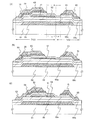
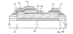
図1(A)に示す薄膜トランジスタは、基板01上にゲート電極05が形成され、ゲート電極05上にゲート絶縁層09a、09bが形成され、ゲート絶縁層09b上に、導電層51が形成され、導電層51上にバッファ層53が形成される。このバッファ層53は、導電層51と略重畳して設けられる。また、導電層51及びバッファ層53の側面及び上面を覆う非晶質半導体層55が形成される。非晶質半導体層55上に、ソース領域とドレイン領域を形成する一導電型を付与する不純物元素が添加された一対の不純物半導体層59、61が形成され、一導電型を付与する不純物元素が添加された一対の不純物半導体層59、61上に配線63、65が形成される。また、一導電型を付与する不純物元素が添加された一対の不純物半導体層59、61の一方61は、バッファ層53に重ならない。また、一導電型を付与する不純物元素が添加された一対の不純物半導体層59、61の他方59の一端部は、バッファ層53に重なっている。
In the thin film transistor illustrated in FIG. 1A, a
導電層51は、電気伝導率が0.1Scm−1以上1.8Scm−1以下の導電層で形成する。導電層51としては、上記電気伝導率を満たす金属層、金属窒化物層、金属炭化物層、金属ホウ化物層、金属珪化物層、ドナーとなる不純物元素が添加された半導体層等がある。
The
金属層としては、代表的には、アルミニウム、銅、チタン、ネオジム、スカンジウム、モリブデン、タンタル、タングステン、コバルト、ニッケル、銀、金、白金、スズ、イリジウム等の金属層またはこれらの複数からなる金属合金層を適宜用いることができる。また、上記金属層または金属合金層の単層または積層で形成することができる。 As the metal layer, typically, a metal layer such as aluminum, copper, titanium, neodymium, scandium, molybdenum, tantalum, tungsten, cobalt, nickel, silver, gold, platinum, tin, iridium, or a metal composed of a plurality of these. An alloy layer can be used as appropriate. Alternatively, the metal layer or the metal alloy layer can be formed as a single layer or a stacked layer.
金属窒化物層としては、窒化チタン層、窒化ジルコニウム層、窒化ハフニウム層、窒化タンタル層、窒化バナジウム層、窒化ニオブ層、窒化クロム層、窒化ランタン層、窒化イットリウム層等を用いることができる。また、上記金属窒化物層の単層または積層で形成することができる。 As the metal nitride layer, a titanium nitride layer, a zirconium nitride layer, a hafnium nitride layer, a tantalum nitride layer, a vanadium nitride layer, a niobium nitride layer, a chromium nitride layer, a lanthanum nitride layer, an yttrium nitride layer, or the like can be used. The metal nitride layer can be formed as a single layer or a stacked layer.
金属炭化物層としては、炭化チタン層、炭化ハフニウム層、炭化ニオブ層、炭化タンタル層、炭化バナジウム層、炭化ジルコニウム層、炭化クロム層、炭化コバルト層、炭化モリブデン層、炭化タングステン層等を用いることができる。また、上記金属炭化物層の単層または積層で形成することができる。 As the metal carbide layer, a titanium carbide layer, a hafnium carbide layer, a niobium carbide layer, a tantalum carbide layer, a vanadium carbide layer, a zirconium carbide layer, a chromium carbide layer, a cobalt carbide layer, a molybdenum carbide layer, a tungsten carbide layer, or the like may be used. it can. Moreover, it can form by the single layer or laminated | stacked of the said metal carbide layer.
金属ホウ化物層としては、ホウ化チタン層を用いることができる。 A titanium boride layer can be used as the metal boride layer.
金属珪化物層としては、珪化白金層、珪化チタン層、珪化モリブデン層、珪化ニッケル層、珪化クロム層、珪化コバルト層、珪化バナジウム層、珪化タングステン層、珪化ジルコニウム層、珪化ハフニウム層、珪化ニオブ層、珪化タンタル層等を用いることができる。また、上記金属珪化物層の単層または積層で形成することができる。 As the metal silicide layer, platinum silicide layer, titanium silicide layer, molybdenum silicide layer, nickel silicide layer, chromium silicide layer, cobalt silicide layer, vanadium silicide layer, tungsten silicide layer, zirconium silicide layer, hafnium silicide layer, niobium silicide layer A tantalum silicide layer or the like can be used. Moreover, it can form by the single layer or laminated | stacked of the said metal silicide layer.
さらには、導電層51を金属層、金属窒化物層、金属炭化物層、金属ホウ化層、金属珪化物層の複数を用いた積層構造とすることができる。
Furthermore, the
なお、導電層51として、金属層、金属窒化物層、金属炭化物層、金属ホウ化物層、金属珪化物層を形成する場合、非晶質半導体層55とオーミック接触させるために、金属層、金属窒化物層、金属炭化物層、金属ホウ化物層、金属珪化物層等のいずれか上に、ドナーとなる不純物元素またはアクセプターとなる不純物元素が添加された半導体層72aを形成した積層構造としてもよい(図32(A)参照)。また、ドナーとなる不純物元素またはアクセプターとなる不純物元素が添加された半導体層72cは、金属層、金属窒化物層、金属炭化物層、金属ホウ化物層、金属珪化物層等のいずれかの上面及び側面を覆っても良い(図32(B)参照)。また、ゲート絶縁層09b上にドナーとなる不純物元素またはアクセプターとなる不純物元素が添加された半導体層72eを形成し、その上に金属層、金属窒化物層、金属炭化物層、金属ホウ化物層、金属珪化物層のいずれかを形成する積層構造としてもよい(図32(C)参照)。このような構造とすることで、金属層、金属窒化物層、金属炭化物層、金属ホウ化物層、金属珪化物層等のいずれかと非晶質半導体層との界面におけるショットキー接合をオーミック接合にすることが可能となり、薄膜トランジスタの特性が向上する。
In the case where a metal layer, a metal nitride layer, a metal carbide layer, a metal boride layer, or a metal silicide layer is formed as the
不純物半導体層には、キャリアとして電子を供給する元素であるドナーが添加されている。ドナーとなる不純物元素は、代表的には周期表第15族元素であるリン、砒素、アンチモン等がある。ドナーとなる不純物元素が添加された半導体層としては、アモルファスシリコン層、アモルファスシリコンゲルマニウム層、アモルファスゲルマニウム層、微結晶シリコン層、微結晶シリコンゲルマニウム層、微結晶ゲルマニウム層、多結晶シリコン層、多結晶シリコンゲルマニウム層、多結晶ゲルマニウム層等で形成される。また、半導体層がアモルファスゲルマニウム層及び微結晶ゲルマニウム層の場合は、抵抗率が低いため、ドナーとなる不純物元素を含まなくともよい。
A donor, which is an element that supplies electrons as carriers, is added to the impurity semiconductor layer. Typical examples of the impurity element that serves as a donor include phosphorus, arsenic, and antimony, which are
ドナーとなる不純物元素が添加された半導体層に添加されるドナーとなる不純物元素の濃度を、二次イオン質量分析法(SIMS:Secondary Ion Mass Spectroscopy)で測定した場合に1×10¹⁸atoms/cm3以上2×1020atoms/cm3以下とすることにより、ゲート絶縁層09bとドナーとなる不純物元素が添加された半導体層の界面における抵抗を低減することが可能であり、また、高速動作が可能であり、オン電流の高い薄膜トランジスタを作製することができる。
When the concentration of the impurity element serving as a donor added to the semiconductor layer to which the impurity element serving as a donor is added is measured by secondary ion mass spectrometry (SIMS), 1 × 10 18 atoms / cm By setting the number to 3 or more and 2 × 10 20 atoms / cm 3 or less, the resistance at the interface between the
ここでの微結晶半導体とは、非晶質と結晶構造(単結晶、多結晶を含む)の中間的な構造の半導体である。この半導体は、自由エネルギー的に安定な第3の状態を有する半導体であって、短距離秩序を持ち格子歪みを有する結晶質なものであり、粒径が2nm以上200nm以下、あるいは10nm以上80nm以下、あるいは20nm以上50nm以下の柱状または針状結晶が基板表面に対して法線方向に成長している。また、電気伝導度が概略10−7S/cmから10−4S/cmであるものが、価電子制御により101S/cm程度にまで高められる半導体を指す。また、複数の微結晶半導体の間に非単結晶半導体が存在している。微結晶半導体の代表例である微結晶シリコンは、そのラマンスペクトルのピークが単結晶シリコンを示す520cm−1よりも低波数側に、シフトしている。即ち、単結晶シリコンを示す520cm−1とアモルファスシリコンを示す480cm−1の間に微結晶シリコンのラマンスペクトルのピークがある。また、未結合手(ダングリングボンド)を終端するため水素またはハロゲンを少なくとも1原子%またはそれ以上含ませてもよい。さらに、ヘリウム、アルゴン、クリプトン、ネオンなどの希ガス元素を含ませてもよく、これにより格子歪みをさらに助長させることで、微結晶の構造の安定性が増し良好な微結晶半導体が得られる。このような微結晶半導体に関する記述は、例えば、米国特許4,409,134号で開示されている。尤も、微結晶半導体の概念は前記した結晶粒径、電気伝導度の値のみに固定されるものではなく、同等の物性値を有するものであれば他の半導体材料に置換することもできる。 The microcrystalline semiconductor here is a semiconductor having an intermediate structure between amorphous and crystalline structures (including single crystal and polycrystal). This semiconductor is a semiconductor having a third state which is stable in terms of free energy, and is a crystalline one having a short-range order and having a lattice distortion, and has a particle size of 2 nm to 200 nm, or 10 nm to 80 nm. Alternatively, columnar or needle-like crystals having a diameter of 20 nm or more and 50 nm or less grow in a normal direction with respect to the substrate surface. In addition, a semiconductor whose electrical conductivity is approximately 10 −7 S / cm to 10 −4 S / cm indicates a semiconductor that can be increased to about 10 1 S / cm by valence electron control. In addition, a non-single-crystal semiconductor exists between the plurality of microcrystalline semiconductors. Microcrystalline silicon, which is a typical example of a microcrystalline semiconductor, has its Raman spectrum peak shifted to a lower wave number side than 520 cm −1 indicating single crystal silicon. That is, the peak of the Raman spectrum of microcrystalline silicon is between 520 cm −1 indicating single crystal silicon and 480 cm −1 indicating amorphous silicon. Further, in order to terminate dangling bonds (dangling bonds), hydrogen or halogen may be contained at least 1 atomic% or more. Further, a rare gas element such as helium, argon, krypton, or neon may be included. By further promoting the lattice distortion, the stability of the microcrystalline structure is increased, and a good microcrystalline semiconductor can be obtained. A description of such a microcrystalline semiconductor is disclosed in, for example, US Pat. No. 4,409,134. However, the concept of the microcrystalline semiconductor is not limited only to the values of the crystal grain size and electric conductivity described above, and can be replaced with other semiconductor materials as long as they have equivalent physical property values.
導電層51の厚さは5nm以上50nm以下、好ましくは5nm以上30nm以下で形成する。
The thickness of the
また、導電層51がドナーとなる不純物元素が添加された半導体層の場合、酸素濃度、及び窒素濃度は、ドナーとなる不純物元素の濃度の10倍未満、代表的には3×10¹⁹atoms/cm3未満、更に好ましくは3×1018atoms/cm3未満、炭素の濃度を3×1018atoms/cm3以下とすることが好ましい。酸素、窒素、及び炭素が、ドナーとなる不純物元素が添加された半導体層に混入する濃度を低減することで、ドナーとなる不純物元素が添加された半導体層が微結晶半導体層の場合、微結晶半導体層の欠陥の生成を抑制する事ができる。さらには、酸素、及び窒素が微結晶半導体層中に入っていると、結晶化しにくい。このため、ドナーとなる不純物元素が添加された半導体層が微結晶半導体層の場合、微結晶半導体層中の酸素濃度、窒素濃度が比較的低く、且つドナーとなる不純物元素を添加することで、微結晶半導体層の結晶性を高めることができる。
In the case where the
また、導電層51がドナーとなる不純物元素が添加された半導体層の場合、ドナーとなる不純物元素が添加された半導体層に、アクセプターとなる不純物元素を、成膜と同時に、或いは成膜後に添加することで、しきい値電圧を制御することが可能となる。アクセプターとなる不純物元素としては、代表的には硼素であり、B2H6、BF3などの不純物気体を1ppm〜1000ppm、好ましくは1〜100ppmの割合で水素化シリコンに混入させると良い。そしてボロンの濃度は、ドナーとなる不純物元素の10分の1程度、例えば1×10¹⁴〜6×10¹⁶atoms/cm3とすると良い。
In the case where the
バッファ層53は、非晶質半導体層を用いて形成する。または、フッ素、塩素等のハロゲンが添加される非晶質半導体層を用いる。バッファ層53の厚さを30nm〜200nm、好ましくは50nm〜150nmとする。非晶質半導体層としては、アモルファスシリコン層、またはゲルマニウムを含むアモルファスシリコン層等がある。
The
バッファ層53の側面を30〜60°に傾斜させることで、導電層51が微結晶半導体層の場合、当該微結晶半導体層を結晶成長核として、微結晶半導体層に接する非晶質半導体層55の界面の結晶性を高めることができるため、薄膜トランジスタの高速動作が可能であり、オン電流を高めることができる。
By tilting the side surface of the
導電層51が微結晶半導体層の場合、バッファ層53として、非晶質半導体層、更には水素、窒素、またはハロゲンを含む非晶質半導体層を形成することで、ドナーとなる不純物元素が添加される半導体層の結晶粒の表面の自然酸化を防止することが可能である。特に、微結晶半導体層において、非晶質半導体と微結晶粒が接する領域では、局部応力により亀裂が入りやすい。この亀裂が酸素に触れると結晶粒は酸化され、結晶粒の表面に酸化シリコンが形成される。しかしながら、ドナーとなる不純物元素が添加された半導体層の表面にバッファ層53を形成することで、微結晶粒の酸化を防ぐことができる。このため、キャリアが捕獲される欠陥、またはキャリアの進行を妨げる領域を低減することができ、薄膜トランジスタの高速動作が可能であり、オン電流を高めることができる。
When the
非晶質半導体層55は、アモルファスシリコン層、またはゲルマニウムを含むアモルファスシリコン層等がある。また、非晶質半導体層55にフッ素、塩素等が含まれていても良い。また、導電層51にドナーとなる不純物元素が添加された半導体層が形成された場合、ドナーとなる不純物元素が添加された半導体層より低い濃度のリンが添加された非晶質半導体層を用いてもよい。また、配線と重複する非晶質半導体層55の厚さを50nm以上500nm未満とする。
The
非晶質半導体層55は、導電層51及びバッファ層53の側面を覆う。また、導電層51の周辺部において、ゲート絶縁層09bと非晶質半導体層55が接する。これらの構造により、導電層51と、一導電型を付与する不純物元素が添加された一対の不純物半導体層59、61とが隔離され、導電層51と、一導電型を付与する不純物元素が添加された一対の不純物半導体層59、61との間で生じるリーク電流を低減することができる。また、非晶質半導体層55は、バッファ層53と重なっていることが好ましい。非晶質半導体層55がバッファ層53と重なることにより、一導電型を付与する不純物元素が添加された一対の不純物半導体層59、61と、バッファ層53が直接接しないため、リーク電流を低減することができる。
The
また、ゲート絶縁層09bが酸化珪素層または窒化珪素層の場合、導電層51にドナーとなる不純物元素が添加された半導体層を用いた場合、ドナーとなる不純物元素が添加された半導体層より低い濃度のリンが添加された非晶質半導体層を非晶質半導体層55として用いることで、しきい値電圧の変動を低減することが可能である。
Further, in the case where the
基板01は、バリウムホウケイ酸ガラス、アルミノホウケイ酸ガラス、若しくはアルミノシリケートガラスなど、フュージョン法やフロート法で作製される無アルカリガラス基板、セラミック基板の他、本作製工程の処理温度に耐えうる耐熱性を有するプラスチック基板等を用いることができる。また、ステンレス合金などの金属基板の表面に絶縁層を設けた基板を適用しても良い。基板01がマザーガラスの場合、基板の大きさは、第1世代(320mm×400mm)、第2世代(400mm×500mm)、第3世代(550mm×650mm)、第4世代(680mm×880mm、または730mm×920mm)、第5世代(1000mm×1200mmまたは1100mm×1250mm)、第6世代1500mm×1800mm)、第7世代(1900mm×2200mm)、第8世代(2160mm×2460mm)、第9世代(2400mm×2800mm、2450mm×3050mm)、第10世代(2950mm×3400mm)等を用いることができる。
The
ゲート電極05は、金属材料で形成される。金属材料としてはアルミニウム、クロム、チタン、タンタル、モリブデン、銅などが適用される。ゲート電極05の好適例は、アルミニウムまたはアルミニウムとバリア金属の積層構造体によって形成される。バリア金属としては、チタン、モリブデン、クロムなどの高融点金属が適用される。バリア金属はアルミニウムのヒロック防止、酸化防止のために設けることが好ましい。
The
ゲート電極05は厚さ50nm以上300nm以下で形成する。ゲート電極05の厚さを50nm以上100nm以下とすることで、後に形成される半導体層や配線の段切れ防止が可能である。また、ゲート電極05の厚さを150nm以上300nm以下とすることで、ゲート電極05の抵抗を低減することが可能であり、基板の大面積化が可能である。
The
なお、ゲート電極05上には半導体層や配線を形成するので、段切れ防止のため端部がテーパー状になるように加工することが望ましい。また、図示しないがこの工程でゲート電極に接続する配線や容量配線も同時に形成することができる。
Note that since a semiconductor layer and a wiring are formed over the
ゲート絶縁層09a、09bはそれぞれ、厚さ50〜150nmの酸化シリコン層、窒化シリコン層、酸化窒化シリコン層、または窒化酸化シリコン層で形成することができる。ここでは、ゲート絶縁層09aとして窒化シリコン層または窒化酸化シリコン層を形成し、ゲート絶縁層09bとして酸化シリコン層または酸化窒化シリコン層を形成して積層する形態を示す。なお、ゲート絶縁層を2層とせず、ゲート絶縁層を、酸化シリコン層、窒化シリコン層、酸化窒化シリコン層、または窒化酸化シリコン層の単層で形成することができる。
Each of the
ゲート絶縁層09aを窒化シリコン層、または窒化酸化シリコン層を用いて形成することで、基板01とゲート絶縁層09aの密着力が高まり、基板01としてガラス基板を用いた場合、基板01からの不純物が、導電層51、バッファ層53、及び非晶質半導体層55に拡散するのを防止することが可能であり、さらにゲート電極05の酸化防止が可能である。即ち、膜剥れを防止することができると共に、後に形成される薄膜トランジスタの電気特性を向上させることができる。また、ゲート絶縁層09a、09bはそれぞれ厚さ50nm以上であると、ゲート電極05の凹凸による被覆率の低減を緩和することが可能であるため好ましい。
When the
ここでは、酸化窒化シリコン層とは、その組成として、窒素よりも酸素の含有量が多いものであって、ラザフォード後方散乱法(RBS:Rutherford Backscattering Spectrometry)及び水素前方散乱法(HFS:Hydrogen Forward Scattering)を用いて測定した場合に、組成範囲として酸素が50〜70原子%、窒素が0.5〜15原子%、Siが25〜35原子%、水素が0.1〜10原子%の範囲で含まれるものをいう。また、窒化酸化シリコン層とは、その組成として、酸素よりも窒素の含有量が多いものであって、RBS及びHFSを用いて測定した場合に、組成範囲として酸素が5〜30原子%、窒素が20〜55原子%、Siが25〜35原子%、水素が10〜30原子%の範囲で含まれるものをいう。但し、酸化窒化シリコンまたは窒化酸化シリコンを構成する原子の合計を100原子%としたとき、窒素、酸素、シリコン及び水素の含有比率が上記の範囲内に含まれるものとする。 Here, the silicon oxynitride layer has a composition that contains more oxygen than nitrogen, and includes Rutherford Backscattering Spectroscopy (RBS) and Hydrogen Forward Scattering (HFS). ) In the range of 50 to 70 atomic% for oxygen, 0.5 to 15 atomic% for nitrogen, 25 to 35 atomic% for Si, and 0.1 to 10 atomic% for hydrogen. It means what is included. In addition, the silicon nitride oxide layer has a nitrogen content higher than that of oxygen as a composition. When measured using RBS and HFS, the composition range is 5 to 30 atomic% oxygen, nitrogen. In the range of 20 to 55 atomic%, Si in the range of 25 to 35 atomic%, and hydrogen in the range of 10 to 30 atomic%. However, when the total number of atoms constituting silicon oxynitride or silicon nitride oxide is 100 atomic%, the content ratio of nitrogen, oxygen, silicon, and hydrogen is included in the above range.
一導電型を付与する不純物元素が添加された一対の不純物半導体層59、61は、nチャネル型の薄膜トランジスタを形成する場合には、代表的な不純物元素としてリンを添加すれば良く、水素化シリコンにPH3などの不純物気体を加えれば良い。また、pチャネル型の薄膜トランジスタを形成する場合には、代表的な不純物元素としてボロンを添加すれば良く、水素化シリコンにB2H6などの不純物気体を加えれば良い。リンまたはボロンの濃度を1×10¹⁹〜1×10²¹atoms/cm3とすることで、配線63、65とオーミックコンタクトすることが可能であり、ソース領域及びドレイン領域として機能する。一導電型を付与する不純物元素が添加された一対の不純物半導体層59、61は、微結晶半導体層、または非晶質半導体層で形成することができる。一導電型を付与する不純物元素が添加された一対の不純物半導体層59、61は10nm以上100nm以下、好ましくは30nm以上50nm以下の厚さで形成する。一導電型を付与する不純物元素が添加された一対の不純物半導体層59、61の膜厚を、薄くすることでスループットを向上させることができる。
The pair of impurity semiconductor layers 59 and 61 to which an impurity element imparting one conductivity type is added may be formed by adding phosphorus as a typical impurity element when an n-channel thin film transistor is formed. it may be added and an impurity gas such as PH 3 in. In the case of forming a p-channel thin film transistor, boron may be added as a typical impurity element, and an impurity gas such as B 2 H 6 may be added to silicon hydride. By setting the concentration of phosphorus or boron to 1 × 10 19 to 1 × 10 21 atoms / cm 3 , ohmic contact with the
一導電型を付与する不純物元素が添加された一対の不純物半導体層59、61の一方、ここでは、一導電型を付与する不純物元素が添加された不純物半導体層61は、導電層51に重ならず、導電層51と一定の距離(距離a)を有する。一導電型を付与する不純物元素が添加された不純物半導体層59の端部と導電層51の端部との距離(距離b)より、距離aを小さくすることで、薄膜トランジスタのオフ電流を低減すると共に、オン電流を高め、高速動作させることができる。
One of the pair of impurity semiconductor layers 59 and 61 to which an impurity element imparting one conductivity type is added, here, the
配線63、65は、アルミニウム、銅、若しくは銅、シリコン、チタン、ネオジム、スカンジウム、モリブデンなどの、マイグレーション防止元素、耐熱性向上元素若しくはヒロック防止元素が添加されたアルミニウム合金の単層または積層で形成することが好ましい。また、一導電型を付与する不純物元素が添加された一対の不純物半導体層59、61と接する側の層を、チタン、タンタル、モリブデン、タングステン、またはこれらの元素の窒化物で形成し、その上にアルミニウムまたはアルミニウム合金を形成した積層構造としても良い。更には、アルミニウムまたはアルミニウム合金の上面及び下面を、チタン、タンタル、モリブデン、タングステン、またはこれらの元素の窒化物で挟んだ積層構造としてもよい。ここでは、配線63、65としては、チタン層、アルミニウム層、及びチタン層の積層構造を用いることができる。
The
また、図1(B)に示すように、バッファ層53を設けず、導電層51に接して非晶質半導体層55を形成してもよい。バッファ層53を形成しないことで、スループットを向上させることができる。
In addition, as illustrated in FIG. 1B, the
また、図1(A)に示す薄膜トランジスタは、非晶質半導体層55が、配線63、65と接せず、一導電型を付与する不純物元素が添加された一対の不純物半導体層59、61を介してバッファ層53上に配線63、65が形成される構造を示したが、図1(C)に示すように、非晶質半導体層55の側面が配線63、65と接する構造とすることができる。
In addition, in the thin film transistor illustrated in FIG. 1A, the
また、本実施の形態で示す薄膜トランジスタは、第1の薄膜トランジスタTr01及び第2の薄膜トランジスタTr02が接続されている。第1の薄膜トランジスタTr01は、ゲート電極05、ゲート絶縁層09a、09b、導電層51、バッファ層53、非晶質半導体層55、一導電型を付与する不純物元素が添加された不純物半導体層59、及び配線63で構成される。第2の薄膜トランジスタTr02は、ゲート電極05、ゲート絶縁層09a、09b、非晶質半導体層55、一導電型を付与する不純物元素が添加された不純物半導体層61、及び配線65で構成される。
In the thin film transistor described in this embodiment, the first thin film transistor Tr01 and the second thin film transistor Tr02 are connected. The first thin film transistor Tr01 includes a
第2の薄膜トランジスタTr02は、非晶質半導体層をチャネル形成領域に用いた薄膜トランジスタである。しかしながら、第1の薄膜トランジスタTr01において、キャリアが流れる領域は、導電層51である。当該領域は、電気伝導度が0.1S/cm以上1.8S/cm以下であり、通常の非晶質半導体層及び微結晶半導体層と比較して抵抗率が低い。このため、ゲート電極05に、第2の薄膜トランジスタTr02のしきい値電圧未満の正電圧が印加されている状態でも、導電層51に多数のキャリアが誘起された状態となる。第2の薄膜トランジスタTr02のしきい値電圧以上の正電圧がゲート電極05に印加されると、第2の薄膜トランジスタTr02がオンとなり、導電層51に誘起されていた多数のキャリアが、第1の薄膜トランジスタTr01の配線63または第2の薄膜トランジスタTr02の配線65へ流れる。
The second thin film transistor Tr02 is a thin film transistor in which an amorphous semiconductor layer is used for a channel formation region. However, in the first thin film transistor Tr01, a region where carriers flow is the
本実施の形態の薄膜トランジスタのチャネル長Lは、一導電型を付与する不純物元素が添加された不純物半導体層61の端部の一方と導電層51の端部の一方の距離a、及び一導電型を付与する不純物元素が添加された不純物半導体層59の端部の一方と導電層51の端部の一方との距離bの和である。チャネル長Lに対して、一導電型を付与する不純物元素が添加された不純物半導体層61の端部の一方と導電層51の端部の一方との距離aを短くし、一導電型を付与する不純物元素が添加された不純物半導体層59の端部の一方と導電層51の端部の一方との距離bを長くすることで、オン電流が高くなり、電界効果移動度も高くなる。
The channel length L of the thin film transistor of this embodiment includes a distance a between one end of the
なお、本実施の形態により第2の薄膜トランジスタTr02のチャネル長(即ち、距離a)を短くすることが可能であるため、第2の薄膜トランジスタTr02において短チャネル効果が生じないように、ゲート絶縁層の膜厚を薄くすることが好ましい。 Note that since the channel length (that is, the distance a) of the second thin film transistor Tr02 can be shortened according to this embodiment mode, the gate insulating layer of the second thin film transistor Tr02 is prevented from having a short channel effect. It is preferable to reduce the film thickness.
一方、ゲート電極05に負の電圧を印加すると、導電層51にはキャリアが誘起されたとしても、第2の薄膜トランジスタTr02は非晶質半導体層で形成されるため、第2の薄膜トランジスタTr02が、薄膜トランジスタのオフ電流の流れを妨げ、オフ電流を低減することができる。
On the other hand, when a negative voltage is applied to the
以上のことから、本実施の形態に示す薄膜トランジスタは、オン電流及び電界効果移動度が高く、オフ電流の低い薄膜トランジスタである。 From the above, the thin film transistor described in this embodiment is a thin film transistor with high on-state current and field-effect mobility and low off-state current.
また、ソース領域及びドレイン領域を繋ぐ非晶質半導体層55表面(バックチャネル)は凹凸状となっており、距離が長いため、ソース領域及びドレイン領域の間の非晶質半導体層55表面を流れるリークパスの距離が長くなる。この結果、非晶質半導体層55表面に流れるリーク電流を低減することが可能である。
Further, the surface (back channel) of the
さらには、ゲート電極05と、一導電型を付与する不純物元素が添加された一対の不純物半導体層59、61の間には、ゲート絶縁層09a、09bのほかに非晶質半導体層55が形成されるため、ゲート電極05と、一導電型を付与する不純物元素が添加された一対の不純物半導体層59、61の間隔が広がる。このため、ゲート電極05と、一導電型を付与する不純物元素が添加された一対の不純物半導体層59、61の間に生じる寄生容量を低減することができる。特に、ドレイン側の電圧降下を低減する薄膜トランジスタとすることができる。このため、当該構造を用いた表示装置は、画素の応答速度を向上させることができる。特に、液晶表示装置の画素に形成される薄膜トランジスタの場合、ドレイン電圧の電圧降下を低減できるため、液晶材料の応答速度を上昇させることが可能である。
Further, an
(実施の形態2)
本実施の形態では、導電層51及びバッファ層53の他の形状について、図2を用いて示す。
(Embodiment 2)
In this embodiment mode, other shapes of the
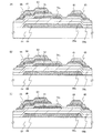
図2に示す薄膜トランジスタは、断面構造において、導電層51aの内側にバッファ層53aが形成されている薄膜トランジスタである。即ち、導電層51aより面積の小さいバッファ層53aが形成され、導電層51aの一部がバッファ層53aより露出している薄膜トランジスタである。このような構造とすることで、導電層51aが微結晶半導体層、金属珪化物層、または金属層の場合、当該微結晶半導体層、金属珪化物層、または金属層を結晶成長核として、導電層51aに接する非晶質半導体層55の結晶性を高めることができるため、薄膜トランジスタの高速動作が可能であり、オン電流を高めることができる。
The thin film transistor illustrated in FIG. 2 is a thin film transistor in which a buffer layer 53a is formed inside a conductive layer 51a in a cross-sectional structure. That is, the thin film transistor has a buffer layer 53a having a smaller area than the conductive layer 51a, and a part of the conductive layer 51a is exposed from the buffer layer 53a. With such a structure, when the conductive layer 51a is a microcrystalline semiconductor layer, a metal silicide layer, or a metal layer, the conductive layer 51a is conductive using the microcrystalline semiconductor layer, the metal silicide layer, or the metal layer as a crystal growth nucleus. Since the crystallinity of the
また、図示しないが、図1及び図2において、導電層51及びバッファ層53の側壁並びに導電層51a及びバッファ層53aの側壁がほぼ垂直、または側面の傾斜角度が80〜100°、好ましくは85〜95°であってもよい。導電層51及びバッファ層53の側壁並びに導電層51a及びバッファ層53aの側壁をほぼ垂直とすることで、薄膜トランジスタが占める面積を縮小することができる。このため、当該薄膜トランジスタを画素に用いた透過型表示装置の開口率を高めることができる。
Although not shown in FIGS. 1 and 2, the side walls of the
なお、本実施の形態は実施の形態1と組み合わせ可能である。
Note that this embodiment mode can be combined with
(実施の形態3)
本実施の形態では、バッファ層の他の形態を図3を用いて示す。本実施の形態では、バッファ層52を絶縁層で形成することを特徴とする。
(Embodiment 3)
In this embodiment mode, another mode of the buffer layer is shown with reference to FIGS. In this embodiment mode, the buffer layer 52 is formed using an insulating layer.
図3(A)に示す薄膜トランジスタは、基板01上にゲート電極05が形成され、ゲート電極05上にゲート絶縁層09a、09bが形成され、ゲート絶縁層09b上に、導電層51が形成され、導電層51上にバッファ層52が形成される。このバッファ層52は、導電層51と略重畳して設けられる。また、導電層51及びバッファ層52の側面及び上面を覆う非晶質半導体層55が形成される。非晶質半導体層55上に一導電型を付与する不純物元素が添加された一対の不純物半導体層59、61が形成され、一導電型を付与する不純物元素が添加された一対の不純物半導体層59、61上に配線63、65が形成される。また、一導電型を付与する不純物元素が添加された一対の不純物半導体層59、61の一方61は、バッファ層53に重ならない。また、一導電型を付与する不純物元素が添加された一対の不純物半導体層59、61の他方59の一端部は、バッファ層53に重なっている。
In the thin film transistor illustrated in FIG. 3A, a
本実施の形態では、バッファ層52を絶縁層で形成する。代表的には、バッファ層52を窒化シリコン層、酸化シリコン層、窒化酸化シリコン層、酸化窒化シリコン層、その他の無機絶縁層を用いて形成する。または、ポリイミド、アクリル樹脂、エポキシ樹脂、その他の有機絶縁層を用いて形成する。また、バッファ層52の厚さを10nm〜150nmとする。バッファ層52を絶縁層で形成することにより、一導電型を付与する不純物元素が添加された一対の不純物半導体層59、61から非晶質半導体層55に流れるリーク電流をバッファ層52でせき止めることが可能であるため、リーク電流を低減することができる。また、オフ電流を低減することができる。
In this embodiment mode, the buffer layer 52 is formed using an insulating layer. Typically, the buffer layer 52 is formed using a silicon nitride layer, a silicon oxide layer, a silicon nitride oxide layer, a silicon oxynitride layer, or another inorganic insulating layer. Alternatively, polyimide, acrylic resin, epoxy resin, or another organic insulating layer is used. Further, the thickness of the buffer layer 52 is set to 10 nm to 150 nm. By forming the buffer layer 52 as an insulating layer, a leak current flowing from the pair of impurity semiconductor layers 59 and 61 to which the impurity element imparting one conductivity type is added to the
また、図3(B)に示すように、導電層51上に半導体層で形成されるバッファ層53が形成され、バッファ層53上に絶縁層で形成されるバッファ層54が形成される。バッファ層54としては、窒化シリコン層、酸化シリコン層、窒化酸化シリコン層、酸化窒化シリコン層、その他の無機絶縁層を用いて形成する。または、ポリイミド、アクリル樹脂、エポキシ樹脂、その他の有機絶縁層を用いて形成する。
As shown in FIG. 3B, a
図3(B)においては、半導体層で形成されるバッファ層53が、絶縁層で形成されるバッファ層54の厚さより厚いが、バッファ層53よりバッファ層54の厚さを厚くしてもよい。なお、バッファ層53及びバッファ層54の合計の膜厚を30nm〜200nm、好ましくは50nm〜150nmとする。導電層51がドナーとなる不純物元素が添加された半導体層の場合、ドナーとなる不純物元素が添加された半導体層上に半導体層で形成されるバッファ層53が形成されることで、ドナーとなる不純物元素が添加された半導体層の酸化を低減することができ、ドナーとなる不純物元素が添加された半導体層の抵抗率の低減を抑制することができる。また、半導体層で形成されるバッファ層53上に絶縁層で形成されるバッファ層54を設けることで、一導電型を付与する不純物元素が添加された一対の不純物半導体層59、61から非晶質半導体層55に流れるリーク電流をバッファ層54でせき止めることが可能であるため、リーク電流を低減することができる。また、オフ電流を低減することができる。
In FIG. 3B, the
なお、本実施の形態は実施の形態1、実施の形態2それぞれと組み合わせ可能である。
Note that this embodiment can be combined with each of
(実施の形態4)
本実施の形態では、導電層51の別の形態を示す。
(Embodiment 4)
In the present embodiment, another form of the
図4(A)に示す薄膜トランジスタは、基板01上にゲート電極05が形成され、ゲート電極05上にゲート絶縁層09a、09bが形成され、ゲート絶縁層09b上に、導電性粒子56が形成され、導電性粒子56及びゲート絶縁層09b上にバッファ層53が形成される。このバッファ層53は、導電性粒子56と略重畳して設けられる。また、バッファ層53の側面及び上面を覆う非晶質半導体層55が形成される。非晶質半導体層55上に一導電型を付与する不純物元素が添加された一対の不純物半導体層59、61が形成され、一導電型を付与する不純物元素が添加された一対の不純物半導体層59、61上に配線63、65が形成される。また、一導電型を付与する不純物元素が添加された一対の不純物半導体層59、61の一方61の両端部は、バッファ層53に重ならない。また、一導電型を付与する不純物元素が添加された一対の不純物半導体層59、61の他方59の一端部は、バッファ層53に重なっている。
In the thin film transistor illustrated in FIG. 4A, a
導電性粒子56は、実施の形態に示す導電層の材料を適宜用いて形成した導電性粒子を用いて形成することができる。また、導電性粒子56がドナーとなる不純物元素が添加された半導体結晶粒の場合、ドナーとなる不純物元素が添加された半導体結晶粒は、シリコン、またはゲルマニウムより多くのシリコンを含むシリコンゲルマニウム(SixGe1−x、0.5<x<1)等で形成することができる。導電性粒子56の大きさを、1〜30nmとし、密度を1×10¹³/cm2未満、好ましくは1×1010/cm2未満とすると、分離された結晶粒を形成することが可能であり、後に形成するバッファ層53とゲート絶縁層09bとの密着性を高めることができる。このため、薄膜トランジスタの歩留まりを高めることができる。
The
導電性粒子56が、金属粒子、金属窒化物粒子、金属炭化物粒子、金属ホウ化物粒子、金属珪化物粒子の場合、スパッタリング法、蒸着法、液滴吐出法、またはCVD法で形成することができる。
When the
ドナーとなる不純物元素が添加された半導体結晶粒の形成方法としては、ドナーとなる不純物元素が添加された微結晶半導体層をスパッタリング法またはプラズマCVD法により成膜した後に、ドナーとなる不純物元素が添加された微結晶半導体層に水素プラズマを曝して、ドナーとなる不純物元素が添加された微結晶半導体層の非晶質半導体成分をエッチングすることで、ドナーとなる不純物元素が添加された半導体結晶粒を形成することができる。または、結晶粒が連続せず分散した状態の厚さで、ドナーとなる不純物元素が添加された微結晶半導体層または結晶性半導体層をスパッタリング法またはプラズマCVD法により成膜することで、ドナーとなる不純物元素が添加された半導体結晶粒を形成することができる。 As a method for forming a semiconductor crystal grain to which an impurity element serving as a donor is added, after forming a microcrystalline semiconductor layer to which an impurity element serving as a donor is added by a sputtering method or a plasma CVD method, The semiconductor crystal to which the impurity element to be added is added by exposing the added microcrystalline semiconductor layer to hydrogen plasma and etching the amorphous semiconductor component of the microcrystalline semiconductor layer to which the impurity element to be donor is added. Grains can be formed. Alternatively, a microcrystalline semiconductor layer or a crystalline semiconductor layer to which an impurity element serving as a donor is added with a thickness in a state where crystal grains are not continuously dispersed is formed by a sputtering method or a plasma CVD method, so that the donor and A semiconductor crystal grain to which an impurity element is added can be formed.
また、導電性粒子56の代わりに、ゲート絶縁層09b上に導電層を形成した後、フォトリソグラフィ工程により形成したレジストマスクを用いて導電層をエッチングして、分離された導電層を形成してもよい。
In addition, instead of the
図4(B)に示す薄膜トランジスタは、基板01上にゲート電極05が形成され、ゲート電極05上にゲート絶縁層09a、09bが形成され、ゲート絶縁層09b上に、導電性粒子56が形成され、導電性粒子56及びゲート絶縁層09b上にバッファ層が形成されず、非晶質半導体層55が形成される。非晶質半導体層55上に一導電型を付与する不純物元素が添加された一対の不純物半導体層59、61が形成され、一導電型を付与する不純物元素が添加された一対の不純物半導体層59、61上に配線63、65が形成される。
In the thin film transistor illustrated in FIG. 4B, a
導電性粒子56は、連続せず、間に非晶質半導体層55が形成されるため、一導電型を付与する不純物元素が添加された一対の不純物半導体層59、61に重畳するように導電性粒子56が形成されていてもオフ電流の上昇を低減することができる。また、バッファ層を形成しないため、フォトマスク数を1枚削減することが可能であり、スループットを向上させると共に、コスト削減が可能である。
Since the
なお、本実施の形態は実施の形態1乃至3のぞれぞれと組み合わせ可能である。
Note that this embodiment can be combined with any of
(実施の形態5)
本実施の形態では、非晶質半導体層の別の形態を示す。
(Embodiment 5)
In this embodiment mode, another form of an amorphous semiconductor layer is shown.
図5に示す薄膜トランジスタは、基板01上にゲート電極05が形成され、ゲート電極05上にゲート絶縁層09a、09bが形成され、ゲート絶縁層09b上に、導電層51が形成され、導電層51上にバッファ層53が形成される。このバッファ層53は、導電層51と略重畳して設けられる。また、導電層51及びバッファ層53の側面及び上面を覆う微結晶半導体層58が形成され、微結晶半導体層58上に非晶質半導体層55が形成される。微結晶半導体層58及び非晶質半導体層55の形状は略同一である。非晶質半導体層55上に一導電型を付与する不純物元素が添加された一対の不純物半導体層59、61が形成され、一導電型を付与する不純物元素が添加された一対の不純物半導体層59、61上に配線63、65が形成される。また、一導電型を付与する不純物元素が添加された一対の不純物半導体層59、61の一方61は、バッファ層53及び導電層51に重ならない。また、一導電型を付与する不純物元素が添加された一対の不純物半導体層59、61の他方59の一端部は、バッファ層53及び導電層51に重なっている。
In the thin film transistor illustrated in FIG. 5, the
微結晶半導体層58は、微結晶シリコン層、微結晶シリコンゲルマニウム層、微結晶ゲルマニウム層で形成することができる。また、導電層51に用いることが可能なドナーとなる不純物元素が添加された半導体層に含むドナーとなる不純物元素濃度より低いドナーとなる不純物元素が添加されてもよい。低濃度のドナーとなる不純物元素が添加されることにより、薄膜トランジスタのしきい値電圧を制御することができる。
The
また、導電層51上にバッファ層53を設けず、導電層に接して微結晶半導体層58を設けてもよい。
Alternatively, the
微結晶半導体層58の厚さを5〜30nm、好ましくは10〜20nmと薄くすることで、薄膜トランジスタのオフ電流を低く保つことができる。また、微結晶半導体層58及び一導電型を付与する不純物元素が添加された一対の不純物半導体層59、61の間に非晶質半導体層55が形成されるため、微結晶半導体層を用いて形成した薄膜トランジスタと比較して、オフ電流を低減することができる。また、非晶質半導体層55及びゲート絶縁層09bの間に、非晶質半導体層と比較して抵抗率の低い微結晶半導体層58を設けることで、キャリアが流れやすくなり、薄膜トランジスタの高速動作が可能である。
By reducing the thickness of the
また、ゲート絶縁層09bを酸化シリコン層または酸化窒化シリコン層とし、微結晶半導体層58として、微結晶シリコン層を形成することで、ゲート絶縁層09bを窒化シリコン層とし、微結晶半導体層を形成せずに非晶質半導体層を形成するときと比べて、しきい値電圧の変動を低減することが可能である。
In addition, the
なお、本実施の形態は実施の形態1乃至4のぞれぞれと組み合わせ可能である。
Note that this embodiment can be combined with any of
(実施の形態6)
本実施の形態では、薄膜トランジスタの構造の別の形態を示す。
(Embodiment 6)
In this embodiment mode, another mode of a thin film transistor structure is shown.
図6に示す薄膜トランジスタは、基板01上にゲート電極05が形成され、ゲート電極05上にゲート絶縁層09a、09bが形成され、ゲート絶縁層09b上に、導電層51eが環状に形成され、導電層51e上にバッファ層53eが環状に形成される。このバッファ層53eは、導電層51eと略重畳して設けられる。また、導電層51e及びバッファ層53eの側面及び上面を覆う非晶質半導体層55が形成される。非晶質半導体層55上に、一導電型を付与する不純物元素が添加された一対の不純物半導体層59、61が形成され、一導電型を付与する不純物元素が添加された一対の不純物半導体層59、61上に配線63、65が形成される。また、一導電型を付与する不純物元素が添加された一対の不純物半導体層59、61の一方61は、バッファ層53eに重ならない。また、一導電型を付与する不純物元素が添加された一対の不純物半導体層59、61の他方59の一端部は、バッファ層53eに重なっている。
In the thin film transistor illustrated in FIG. 6, a
図6に示す薄膜トランジスタは、ソース領域及びドレイン領域が対向するチャネル形成領域が円形であることが特徴である。具体的には、一導電型を付与する不純物元素が添加された一対の不純物半導体層59、61の一方61は円形であり、一導電型を付与する不純物元素が添加された一対の不純物半導体層59、61の他方59は環状である。即ち、ソース領域またはドレイン領域の一方が、ソース領域またはドレイン領域の他方を、一定間隔をあけて囲う構造となっている。このため、配線63をソース配線とし、配線65をドレイン配線とした場合、チャネル形成領域が曲線状であると、しきい値電圧の変動を低減することが可能であり、薄膜トランジスタの特性の信頼性を高めることができる。また、ソース配線及びドレイン配線が直線型である典型的な薄膜トランジスタと比較して、ソース領域及びドレイン領域が曲線状であるとそれらの対向面積が大きくなるため、同じチャネル幅の薄膜トランジスタを設計する場合、薄膜トランジスタの面積を小さくすることができる。
The thin film transistor illustrated in FIG. 6 is characterized in that a channel formation region where a source region and a drain region face each other is circular. Specifically, one of the pair of impurity semiconductor layers 59 and 61 to which an impurity element imparting one conductivity type is added is circular, and a pair of impurity semiconductor layers to which an impurity element imparting one conductivity type is added The other 59 of 59 and 61 is annular. That is, one of the source region and the drain region surrounds the other of the source region and the drain region with a certain interval. Therefore, in the case where the
なお、本実施の形態は実施の形態1乃至5のぞれぞれと組み合わせ可能である。
Note that this embodiment can be combined with any of
(実施の形態7)
本実施の形態では、図1(A)に示すような、高速動作が可能であり、オン電流が高く、且つオフ電流の低い薄膜トランジスタの作製工程について示す。
(Embodiment 7)
In this embodiment, a manufacturing process of a thin film transistor which can operate at high speed, has high on-state current, and low off-state current as illustrated in FIG.
非晶質半導体層または微結晶半導体層を有する薄膜トランジスタは、p型よりもn型の方が、電界効果移動度が高いので駆動回路に用いるのにより適している。同一の基板上に形成する薄膜トランジスタを全て同じ導電型にそろえておくことが、工程数を抑えるためにも望ましい。ここでは、nチャネル型の薄膜トランジスタを用いて説明する。 A thin film transistor including an amorphous semiconductor layer or a microcrystalline semiconductor layer is more suitable for use in a driver circuit because an n-type thin film transistor has higher field-effect mobility than a p-type. In order to reduce the number of steps, it is desirable to arrange all thin film transistors formed on the same substrate to have the same conductivity type. Here, description is made using an n-channel thin film transistor.
図1(A)に示す薄膜トランジスタの作製工程について、図7乃至図10を用いて示す。なお、図7及び図8において左側は図10のA−Bの断面図であり、薄膜トランジスタが形成される領域の断面を示し、右側は図10のC−Dの断面図であり、画素においてゲート配線及びソース配線が交差する領域の断面を示す。 A manufacturing process of the thin film transistor illustrated in FIG. 1A will be described with reference to FIGS. 7 and 8, the left side is a cross-sectional view taken along line AB in FIG. 10, showing a cross section of a region where a thin film transistor is formed, and the right side is a cross-sectional view taken along line CD in FIG. The cross section of the area | region where wiring and source wiring cross | intersect is shown.
図7(A)に示すように、基板01上に導電層03を形成する。導電層03としては、実施の形態1に示すゲート電極05に列挙した材料を用いて形成することができる。導電層03は、スパッタリング法、CVD法、めっき法、印刷法、液滴吐出法等を用いて形成する。
As shown in FIG. 7A, a
次に、第1のフォトマスクを用いたフォトリソグラフィ工程を用いて形成したレジストマスクを用いて導電層03を所望の形状にエッチングして、図7(B)に示すように、ゲート配線05を形成する。この後、レジストマスクを除去する。
Next, the
次に、ゲート配線05及び基板01上にゲート絶縁層09を形成する。ゲート絶縁層09としては、実施の形態1に示すゲート絶縁層09a、09bに列挙した材料を用いて形成することができる。ゲート絶縁層09は、CVD法やスパッタリング法等を用いて形成する。
Next, a
次に、ゲート絶縁層09上に導電層11、及びバッファ層13を積層して形成する。導電層11がドナーとなる不純物元素が添加された半導体層の場合の成膜方法を以下に示す。
Next, the
プラズマCVD装置の反応室内において、シリコンまたはゲルマニウムを含む堆積性気体と、水素とを混合し、グロー放電プラズマにより、微結晶半導体層または非晶質半導体層を形成する。シリコンまたはゲルマニウムを含む堆積性気体の流量に対して、水素の流量を10〜2000倍、好ましくは50〜200倍に希釈して微結晶半導体層を形成する。シリコンまたはゲルマニウムを含む堆積性気体の流量に対して、水素の流量を0〜10倍、好ましくは1〜5倍に希釈して非晶質半導体層を形成する。基板の加熱温度は100℃〜300℃、好ましくは120℃〜220℃で行う。また、上記原料ガスと共に、リン、砒素、アンチモン等を含む気体を混合することで、ドナーとなる不純物元素が添加された半導体層を形成することができる。ここでは、シランと、水素及び/または希ガスと共にフォスフィンを混合して、グロー放電プラズマにより、ドナーとなる不純物元素が添加された半導体層としてリンを含む微結晶シリコン層を形成することができる。
In a reaction chamber of a plasma CVD apparatus, a deposition gas containing silicon or germanium and hydrogen are mixed, and a microcrystalline semiconductor layer or an amorphous semiconductor layer is formed by glow discharge plasma. The microcrystalline semiconductor layer is formed by diluting the flow rate of
ドナーとなる不純物元素が添加された半導体層の形成工程においてグロー放電プラズマの生成は、3MHzから30MHz程度までのHF(high frequency)帯、代表的には13.56MHz、27.12MHzの高周波電力、または30MHzより大きく300MHz程度までのVHF(very high frequency)帯の高周波電力、代表的には60MHzを印加することで行われる。 In the process of forming a semiconductor layer to which an impurity element serving as a donor is added, glow discharge plasma is generated in an HF (high frequency) band from 3 MHz to 30 MHz, typically high frequency power of 13.56 MHz and 27.12 MHz, Alternatively, it is performed by applying high-frequency power in a VHF (very high frequency) band from 30 MHz to about 300 MHz, typically 60 MHz.
また、シリコンまたはゲルマニウムを含む堆積性気体の代表例としては、SiH4、Si2H6、GeH4、Ge2H6等がある。 Typical examples of the deposition gas containing silicon or germanium include SiH 4 , Si 2 H 6 , GeH 4 , and Ge 2 H 6 .
なお、ドナーとなる不純物元素が添加された半導体層を形成する代わりに、ゲート絶縁層09としてドナーとなる不純物元素が添加された絶縁層を形成し、その上にドナーとなる不純物元素を含まない半導体層を形成してもよい。例えば、ドナーとなる不純物元素(リン、砒素、またはアンチモン)を含む酸化シリコン層、窒化シリコン層、酸化窒化シリコン層、または窒化酸化シリコン層等をゲート絶縁層として形成することができる。また、ゲート絶縁層09を積層構造とする場合、微結晶半導体層に接する層または基板01に接する層にドナーとなる不純物元素を添加してもよい。
Note that instead of forming a semiconductor layer to which an impurity element serving as a donor is added, an insulating layer to which an impurity element serving as a donor is added is formed as the
ゲート絶縁層09としてドナーとなる不純物元素が添加された絶縁層の形成方法としては、絶縁層の原料気体と共に、ドナーとなる不純物元素を含む気体を用いて絶縁層を形成すればよい。例えば、シラン、アンモニア、及びフォスフィンを用いたプラズマCVD法によりリンを含む窒化シリコン層を形成することができる。また、シラン、一酸化二窒素、及びアンモニア、並びにフォスフィンを用いたプラズマCVD法により、リンを含む酸化窒化シリコン層を形成することができる。
As a method for forming an insulating layer to which an impurity element serving as a donor is added as the
また、ゲート絶縁層09を形成する前に、成膜装置の反応室内にドナーとなる不純物元素を含む気体を流し、基板01表面及び反応室内壁にドナーとなる不純物元素を吸着させてもよい。この後、ゲート絶縁層09を形成することで、ドナーとなる不純物元素を取り込みながら絶縁層が堆積するため、ドナーとなる不純物元素が添加された絶縁層を形成することができる。
Alternatively, before the
また、ドナーとなる不純物元素が添加された半導体層を形成する前に、成膜装置の反応室内にドナーとなる不純物元素を含む気体を流し、ゲート絶縁層09及び反応室内壁にドナーとなる不純物元素を吸着させてもよい。この後、半導体層を堆積することで、ドナーとなる不純物元素を取り込みながら半導体層が堆積するため、ドナーとなる不純物元素が添加された半導体層を形成することができる。
Further, before forming a semiconductor layer to which an impurity element serving as a donor is added, a gas containing an impurity element serving as a donor is flowed into the reaction chamber of the deposition apparatus, and the impurity serving as a donor is formed on the
また、導電層11として、金属層、金属窒化物層、金属炭化物層、金属ホウ化物層、金属珪化物層を形成する場合、スパッタリング法、蒸着法、CVD法、液滴吐出法、印刷法等により導電層を形成する。
Moreover, when forming a metal layer, a metal nitride layer, a metal carbide layer, a metal boride layer, a metal silicide layer as the
なお、ゲート絶縁層09が酸化シリコン層、または酸化窒化シリコン層の場合、導電層11を形成する前に、ゲート絶縁層09の表面をプラズマ処理してもよい。代表的には、水素プラズマ、アンモニアプラズマ、H2Oプラズマ、ヘリウムプラズマ、アルゴンプラズマ、ネオンプラズマ等のプラズマをゲート絶縁層09表面に曝す。この結果、ゲート絶縁層表面の欠陥を低減することができる。代表的には、ゲート絶縁層09表面のダングリングボンドを終端化することができる。この後、導電層または非晶質半導体層を形成すると、導電層または非晶質半導体の界面における欠陥を低減することが可能である。この結果、欠陥によるキャリアの捕獲を低減することが可能であり、オン電流を高めることが可能である。
Note that in the case where the
次に、バッファ層13を形成する。バッファ層13として半導体層を形成する場合、シリコン、またはゲルマニウムを含む堆積性気体を用いたプラズマCVD法により非晶質半導体層を形成することができる。または、シリコン、またはゲルマニウムを含む堆積性気体に、ヘリウム、アルゴン、クリプトン、ネオンから選ばれた一種または複数種の希ガス元素で希釈して非晶質半導体層を形成することができる。または、シランガスの流量の0倍以上10倍以下、更に好ましくは1倍以上5倍以下の流量の水素を用いて、水素を含む非晶質半導体層を形成することができる。また、上記水素化半導体層に、フッ素、塩素等のハロゲンを添加してもよい。
Next, the
また、非晶質半導体層は、ターゲットにシリコン、ゲルマニウム等の半導体ターゲットを用いて水素、または希ガスでスパッタリングして非晶質半導体層を形成することができる。 The amorphous semiconductor layer can be formed by sputtering with hydrogen or a rare gas using a semiconductor target such as silicon or germanium as a target.
バッファ層13として絶縁層を形成する場合、ゲート絶縁層09と同様に形成することができる。または、ポリイミド、アクリル樹脂、エポキシ樹脂、その他の有機絶縁層の原料を塗布した後、焼成して絶縁層を形成することができる。
In the case where an insulating layer is formed as the
また、導電層11がドナーとなる不純物元素が添加された半導体層の場合、プラズマCVD法によりバッファ層13を300℃〜400℃の温度にて成膜することが好ましい。この成膜処理により水素がドナーとなる不純物元素が添加された半導体層に供給され、ドナーとなる不純物元素が添加された半導体層を水素化したのと同等の効果が得られる。すなわち、ドナーとなる不純物元素が添加された半導体層上にバッファ層13を堆積することにより、ドナーとなる不純物元素が添加された半導体層に水素を拡散させて、ダングリングボンドの終端をすることができる。
In the case where the
ドナーとなる不純物元素が添加された半導体層が微結晶半導体層で形成される場合、ドナーとなる不純物元素が添加された半導体層の表面に、バッファ層13として非晶質半導体層、更には水素、窒素、またはハロゲンを含む非晶質半導体層を形成することで、ドナーとなる不純物元素が添加された半導体層に含まれる結晶粒の表面の自然酸化を防止することが可能である。特に、非晶質半導体と微結晶粒が接する領域では、局部応力により亀裂が入りやすい。この亀裂が酸素に触れると結晶粒は酸化され、結晶粒の表面に酸化シリコンが形成される。しかしながら、ドナーとなる不純物元素が添加された半導体層の表面に非晶質半導体層を形成することで、微結晶粒の酸化を防ぐことができる。また、薄膜トランジスタへの印加電圧の高い(例えば15V程度)表示装置、代表的には液晶表示装置において、バッファ層の厚さを厚くすると、ドレイン耐圧が高くなり、薄膜トランジスタに高い電圧が印加されても、薄膜トランジスタが劣化することを低減することができる。
In the case where a semiconductor layer to which an impurity element that serves as a donor is added is formed using a microcrystalline semiconductor layer, an amorphous semiconductor layer as a
次に、バッファ層13上にレジストを塗布した後、第2のフォトマスクを用いたフォトリソグラフィ工程を用いて形成したレジストマスクを用いて、バッファ層13及び導電層11を所望の形状にエッチングして、図7(C)に示すように、薄膜トランジスタを形成する領域において、導電層51、及びバッファ層19を形成する。また、ゲート配線及びソース配線が交差する領域において、導電層17、及びバッファ層21を形成する。この後、レジストマスクを除去する。
Next, after applying a resist on the
次に、図7(D)に示すように、非晶質半導体層23、及び一導電型を付与する不純物元素が添加された不純物半導体層25を形成する。
Next, as illustrated in FIG. 7D, an
非晶質半導体層23としては、バッファ層13として半導体層を用いて形成する場合と同様に形成することができる。
The
なお、非晶質半導体層23を形成する際、プラズマCVD装置の成膜室内壁に窒化酸化シリコン層、窒化シリコン層、酸化シリコン層、酸化窒化シリコン層をプリコートした後に、シリコンまたはゲルマニウムを含む堆積性気体の流量に対して、水素の流量を10〜2000倍、好ましくは50〜200倍に希釈して半導体層を成膜すると、膜中に成膜室内壁の酸素、窒素等を取り込みながら膜が堆積するため、結晶化せず、緻密な非晶質半導体層を形成することができる。なお、当該半導体層に微結晶が含まれる場合もある。また、ゲート絶縁層09が窒化シリコン層の場合は、当該成膜方法により非晶質半導体層を形成することで、膜剥れが生じず、歩留まりを高めることができる。
Note that when the
ここでは、nチャネル型の薄膜トランジスタを形成するため、一導電型を付与する不純物元素が添加された不純物半導体層25としては、シリコンまたはゲルマニウムを含む堆積性気体と、フォスフィンとを用いたプラズマCVD法により形成する。また、pチャネル型の薄膜トランジスタを形成する場合は、シリコンまたはゲルマニウムを含む堆積性気体と、ジボランとを用いたプラズマCVD法により形成する。
Here, a plasma CVD method using a deposition gas containing silicon or germanium and phosphine is used as the
導電層11、バッファ層13、非晶質半導体層23、及び一導電型を付与する不純物元素が添加された不純物半導体層25の形成工程においてグロー放電プラズマの生成は、3MHzから30MHz程度までのHF帯、代表的には13.56MHz、27.12MHzの高周波電力、または30MHzより大きく300MHz程度までのVHF帯の高周波電力、代表的には60MHzを印加することで行われる。
In the process of forming the
導電層27としては、実施の形態1に示す配線63、65に列挙した材料を用いて形成することができる。導電層27は、CVD法やスパッタリング法、印刷法、液滴吐出法等を用いて形成する。
The
次に、導電層27上にレジストを塗布する。レジストは、ポジ型レジストまたはネガ型レジストを用いることができる。ここでは、ポジ型レジストを用いて示す。
Next, a resist is applied on the
次に、第3のフォトマスクとして多階調マスクを用いて、レジストに光を照射した後現像して、レジストマスク29を形成する。
Next, using a multi-tone mask as a third photomask, the resist is irradiated with light and then developed to form a resist
ここで、多階調マスクを用いた露光について、図9を用いて説明する。 Here, exposure using a multi-tone mask will be described with reference to FIG.
多階調マスクとは、露光部分、中間露光部分、及び未露光部分に3つの露光レベルを行うことが可能なマスクであり、一度の露光及び現像工程により、複数(代表的には二種類)の厚さの領域を有するレジストマスクを形成することが可能である。このため、多階調マスクを用いることで、フォトマスクの枚数を削減することが可能である。 A multi-tone mask is a mask capable of performing three exposure levels on an exposed portion, an intermediate exposed portion, and an unexposed portion, and a plurality of (typically two types) can be obtained by one exposure and development process. It is possible to form a resist mask having a region with a thickness of. Therefore, the number of photomasks can be reduced by using a multi-tone mask.
多階調マスクの代表例としては、図9(A)に示すようなグレートーンマスク159a、図9(C)に示すようなハーフトーンマスク159bがある。
Typical examples of the multi-tone mask include a gray-
図9(A)に示すように、グレートーンマスク159aは、透光性を有する基板163及びその上に形成される遮光部164並びに回折格子165で構成される。遮光部164においては、光の透過率が0%である。一方、回折格子165はスリット、ドット、メッシュ等の光透過部の間隔を、露光に用いる光の解像度限界以下の間隔とすることにより、光の透過率を制御することができる。なお、回折格子165は、周期的なスリット、ドット、メッシュ、または非周期的なスリット、ドット、メッシュどちらも用いることができる。
As shown in FIG. 9A, the
透光性を有する基板163は、石英等の透光性を有する基板を用いることができる。遮光部164及び回折格子165は、クロムや酸化クロム等の光を吸収する遮光材料を用いて形成することができる。
As the
グレートーンマスク159aに露光光を照射した場合、図9(B)に示すように、遮光部164においては、光透過率166は0%であり、遮光部164及び回折格子165が設けられていない領域では光透過率166は100%である。また、回折格子165においては、10〜70%の範囲で調整可能である。回折格子165における光の透過率透過率の調整は、回折格子のスリット、ドット、またはメッシュの間隔及びピッチの調整により可能である。
When the gray-
図9(C)に示すように、ハーフトーンマスク159bは、透光性を有する基板163及びその上に形成される半透過部167並びに遮光部168で構成される。半透過部167は、MoSiN、MoSi、MoSiO、MoSiON、CrSiなどを用いることができる。遮光部168は、クロムや酸化クロム等の光を吸収する遮光材料を用いて形成することができる。
As shown in FIG. 9C, the
ハーフトーンマスク159bに露光光を照射した場合、図9(D)に示すように、遮光部168においては、光透過率169は0%であり、遮光部168及び半透過部167が設けられていない領域では光透過率169は100%である。また、半透過部167においては、10〜70%の範囲で調整可能である。半透過部167に於ける光の透過率の調整は、半透過部167の材料により可能である。
When the
多階調マスクを用いて露光した後、現像することで、図7(D)に示すように、膜厚の異なる領域を有するレジストマスク29を形成することができる。
By performing development after exposure using a multi-tone mask, a resist
次に、レジストマスク29により、非晶質半導体層23、一導電型を付与する不純物元素が添加された不純物半導体層25、及び導電層27をエッチングし分離する。この結果、図7(E)に示すような、非晶質半導体層33、35、一導電型を付与する不純物が添加された半導体層37、39、及び導電層41を形成することができる。
Next, the
次に、レジストマスク29をアッシングする。この結果、レジストの面積が縮小し、厚さが薄くなる。このとき、膜厚の薄い領域のレジスト(ゲート配線05の一部と重畳する領域)は除去され、図7(E)に示すように、分離されたレジストマスク45を形成することができる。
Next, the resist
次に、レジストマスク45を用いて、導電層41をエッチングし分離する。この結果、図8(A)に示すような、ソース配線63、ドレイン電極65を形成することができる。レジストマスク45を用いて導電層41をウエットエッチングすると、導電層41が等方的にエッチングされる。この結果、レジストマスク45より面積の小さいソース配線63、及びドレイン電極65を形成することができる。
Next, the
ゲート配線05及び一導電型を付与する不純物元素が添加された不純物半導体層39の交差部においては、ゲート絶縁層09の他に、導電層17、バッファ層21、及び非晶質半導体層35が形成され、ゲート配線05及び一導電型を付与する不純物元素が添加された不純物半導体層39の間隔が広がる。このため、ゲート配線05及び一導電型を付与する不純物元素が添加された不純物半導体層39が交差する領域での寄生容量を低減できる。
At the intersection of the
次に、レジストマスク45を用いて、一導電型を付与する不純物が添加された半導体層37をエッチングして、一導電型を付与する不純物元素が添加された一対の不純物半導体層59、61を形成する。なお、当該エッチング工程において、非晶質半導体層33の一部もエッチングされ、非晶質半導体層55になる。
Next, the resist
ここでは、ソース配線63、及びドレイン電極65の端部と、一導電型を付与する不純物元素が添加された一対の不純物半導体層59、61の端部は一致せずずれており、ソース配線63、ドレイン電極65の端部の外側に、一導電型を付与する不純物元素が添加された一対の不純物半導体層59、61の端部が形成される。この後、レジストマスク45を除去する。
Here, the end portions of the
次に、露出している非晶質半導体層55にH2Oプラズマを照射してもよい。代表的には、気化した水をプラズマで放電して生成したラジカルを、非晶質半導体層55、一導電型を付与する不純物元素が添加された一対の不純物半導体層59、61、及びソース配線63、ドレイン電極65の露出部に照射することで、薄膜トランジスタの高速動作が可能であり、オン電流を更に高めることができる。また、オフ電流を低減することができる。
Next, the exposed
以上の工程により、薄膜トランジスタを形成することができる。 Through the above process, a thin film transistor can be formed.
次に、図8(B)に示すように、ソース配線63、ドレイン電極65、ゲート絶縁層09上に、保護絶縁層67を形成する。保護絶縁層67としては、窒化シリコン層、窒化酸化シリコン層、酸化シリコン層、または酸化窒化シリコン層を用いて形成することができる。なお、保護絶縁層67は、大気中に浮遊する有機物や金属物、水蒸気などの汚染不純物の侵入を防ぐためのものであり、緻密な膜が好ましい。
Next, as illustrated in FIG. 8B, the protective insulating
次に、保護絶縁層67上に平坦化層69を形成してもよい。平坦化層69としては、アクリル樹脂、ポリイミド、エポキシ樹脂、シロキサンポリマー等の有機絶縁層を用いて形成することができる。ここでは、感光性の有機樹脂を用いて平坦化層69を形成する。次に、平坦化層69を第4のフォトマスクを用いて感光した後、現像して、図8(C)に示すように、保護絶縁層67を露出する。次に、平坦化層69を用いて保護絶縁層67をエッチングして、ドレイン電極65の一部を露出するコンタクトホールを形成する。
Next, a
次に、コンタクトホールに画素電極71を形成する。ここでは、平坦化層69上に導電層を形成した後、導電層上にレジストを塗布する。次に、第5のフォトマスクを用いたフォトリソグラフィ工程により形成したレジストマスクを用いて導電層をエッチングして、画素電極71を形成する。
Next, the
画素電極71は、酸化タングステンを含むインジウム酸化物、酸化タングステンを含むインジウム亜鉛酸化物、酸化チタンを含むインジウム酸化物、酸化チタンを含むインジウム錫酸化物、インジウム錫酸化物、インジウム亜鉛酸化物、酸化シリコンが添加されたインジウム錫酸化物などの透光性を有する導電性材料を用いることができる。
The
また、画素電極71として、導電性高分子(導電性ポリマーともいう)を含む導電性組成物を用いて形成することができる。導電性組成物を用いて形成した画素電極は、シート抵抗が10000Ω/□以下、波長550nmにおける透光率が70%以上であることが好ましい。また、導電性組成物に含まれる導電性高分子の抵抗率が0.1Ω・cm以下であることが好ましい。
The
導電性高分子としては、いわゆるπ電子共役系導電性高分子が用いることができる。例えば、ポリアニリンまたはその誘導体、ポリピロールまたはその誘導体、ポリチオフェンまたはその誘導体、若しくはこれらの2種以上の共重合体などがあげられる。 As the conductive polymer, a so-called π-electron conjugated conductive polymer can be used. For example, polyaniline or a derivative thereof, polypyrrole or a derivative thereof, polythiophene or a derivative thereof, or a copolymer of two or more kinds thereof can be given.
ここでは、画素電極71としては、スパッタリング法によりITO膜を成膜した後、ITO膜上にレジストを塗布する。次に、第6のフォトマスクを用いてレジストを露光及び現像し、レジストマスクを形成する。次に、レジストマスクを用いてITO膜をエッチングして画素電極71を形成する。この後、レジストマスクを除去する。なお、図8(C)は、図10のA−B、及びC−Dの断面図に相当する。図10に示す薄膜トランジスタは、ソース領域及びドレイン領域が対向するチャネル形成領域の上面形状が平行型であるが、この代わりにチャネル形成領域の上面形状がC字(U字)状の薄膜トランジスタを作製してもよい。
Here, as the
以上により、オフ電流が低く、オン電流が高く、高速動作が可能である薄膜トランジスタを作製することができる。また、当該薄膜トランジスタを画素電極のスイッチング素子として有する素子基板を作製することができる。なお、本実施の形態においては、通常の逆スタガ型の薄膜トランジスタの作製工程と比較して、導電層及びバッファ層を所定の形状にエッチングするためのフォトマスクが1枚増えるが、一対の非晶質半導体層、一導電型を付与する不純物元素が添加された一対の不純物半導体層、及び配線を所定の形状にエッチングするためのフォトマスクに多階調マスクを用いているため、当該プロセスでフォトマスク数を1枚削減することが可能であるため、作製工程全体としてはマスク枚数が増加していない。 Through the above steps, a thin film transistor with low off-state current, high on-state current, and high-speed operation can be manufactured. In addition, an element substrate having the thin film transistor as a switching element of a pixel electrode can be manufactured. Note that in this embodiment, one photomask for etching a conductive layer and a buffer layer into a predetermined shape is added as compared with a manufacturing process of a normal inverted staggered thin film transistor, but a pair of amorphous films A multi-tone mask is used as a photomask for etching a conductive semiconductor layer, a pair of impurity semiconductor layers to which an impurity element imparting one conductivity type is added, and a wiring into a predetermined shape; Since the number of masks can be reduced by one, the number of masks does not increase in the entire manufacturing process.
(実施の形態8)
本実施の形態では、図1(B)に示すような、非晶質半導体層をチャネル形成領域に有する薄膜トランジスタと比較して高速動作が可能であり、オン電流が高く、且つ微結晶半導体層をチャネル形成領域に有する薄膜トランジスタと比較してオフ電流の低い薄膜トランジスタの作製工程について示す。
(Embodiment 8)
In this embodiment mode, high-speed operation is possible as compared with a thin film transistor including an amorphous semiconductor layer in a channel formation region as illustrated in FIG. 1B, high on-state current, and a microcrystalline semiconductor layer is formed. A manufacturing process of a thin film transistor whose off-state current is lower than that of a thin film transistor included in a channel formation region is described.
なお、図11の左側は図12のA−Bの断面図であり、薄膜トランジスタが形成される領域の断面を示し、右側は図12のC−Dの断面図であり、画素においてゲート配線及びソース配線が交差する領域の断面を示す。 Note that the left side of FIG. 11 is a cross-sectional view taken along the line AB in FIG. 12, showing a cross-section of a region where a thin film transistor is formed, and the right side is a cross-sectional view taken along the line CD in FIG. The cross section of the area | region where wiring cross | intersects is shown.
実施の形態7に示す図7(A)の工程を経て、ゲート配線05を形成する。次に、ゲート配線05及び基板01上にゲート絶縁層09を形成する。
Through the process of FIG. 7A described in
次に、図7(B)の工程を経てゲート絶縁層09上に、導電層11、及びバッファ層13を順に積層する。次に、フォトリソグラフィ工程により形成したレジストマスクを用いて、導電層11、及びバッファ層13をエッチングして、図11(A)に示すように、導電層51、17、及びバッファ層19、21を形成する。
Next, the
次に、非晶質半導体層23及び一導電型を付与する不純物元素が添加された不純物半導体層25を形成する。
Next, an
次に、フォトリソグラフィ工程を用いて形成したレジストマスクを用いて、一導電型を付与する不純物元素が添加された不純物半導体層25、及び非晶質半導体層23を所望の形状にエッチングして、図11(B)に示すように、薄膜トランジスタを形成する領域において、非晶質半導体層81、及び一導電型を付与する不純物元素が添加された不純物半導体層83を形成する。また、ゲート配線及びソース配線が交差する領域において、非晶質半導体層82、及び一導電型を付与する不純物元素が添加された不純物半導体層84を形成する。この後、レジストマスクを除去する。なお、導電層51、17の側面が非晶質半導体層81、82に覆われる。
Next, the
次に、図11(C)に示すように導電層27を形成する。
Next, a
次に、フォトリソグラフィ工程を用いて形成したレジストマスクを用いて導電層27を所望の形状にエッチングして、図11(D)に示すように、ソース配線85及びドレイン電極87を形成する。
Next, the
ゲート配線05及びソース配線85の交差部においては、ゲート絶縁層09の他に、導電層17、バッファ層21、及び非晶質半導体層82が形成され、ゲート配線05及びソース配線85の間隔が広がる。このため、ゲート配線05及びソース配線85が交差する領域での寄生容量を低減できる。
At the intersection of the
次に、レジストマスクを用いて一導電型を付与する不純物元素が添加された不純物半導体層83をエッチングして、一導電型を付与する不純物元素が添加された一対の不純物半導体層91、93を形成する。また、当該エッチング工程において、非晶質半導体層81もエッチングされる。一部エッチングされた、凹部が形成された非晶質半導体層を非晶質半導体層95と示す。ソース領域及びドレイン領域の形成工程と、非晶質半導体層95の凹部とを同一工程で形成することができる。この後、レジストマスクを除去する。
Next, the
次に、露出している非晶質半導体層95にH2Oプラズマを照射してもよい。代表的には、気化した水をプラズマで放電して生成したラジカルを、非晶質半導体層95、一導電型を付与する不純物元素が添加された一対の不純物半導体層91、93、及びソース配線85、ドレイン電極87の露出部に照射することで、薄膜トランジスタの高速動作が可能であり、オン電流を更に高めることができる。また、オフ電流を低減することができる。
Next, the exposed
以上の工程により、高速動作が可能であり、オン電流が高く、オフ電流の低い薄膜トランジスタを形成する。 Through the above steps, a thin film transistor that can operate at high speed, has high on-state current, and low off-state current is formed.
次に、図8(B)及び図8(C)に示す工程を経て、図11(E)に示すように、保護絶縁層67、平坦化層69、及びドレイン電極に接続する画素電極71を形成する。なお、図11(E)は、図12のA−B、及びC−Dの断面図に相当する。図12に示す薄膜トランジスタは、ソース領域及びドレイン領域が直線に対向する、チャネル形成領域の上面形状が直線型であるが、この代わりにチャネル形成領域の上面形状がC字(U字)状の薄膜トランジスタを作製してもよい。
Next, through the steps shown in FIGS. 8B and 8C, as shown in FIG. 11E, the protective insulating
以上により、オフ電流が低く、オン電流が高く、高速動作が可能である薄膜トランジスタを作製することができる。また、当該薄膜トランジスタを画素電極のスイッチング素子として有する素子基板を作製することができる。 Through the above steps, a thin film transistor with low off-state current, high on-state current, and high-speed operation can be manufactured. In addition, an element substrate having the thin film transistor as a switching element of a pixel electrode can be manufactured.
(実施の形態9)
本実施の形態では、チャネル保護型の薄膜トランジスタについて、図33を用いて示す。
(Embodiment 9)
In this embodiment, a channel protective thin film transistor is described with reference to FIGS.
図33に示す薄膜トランジスタは、基板01上にゲート電極05が形成され、ゲート電極05上にゲート絶縁層09a、09bが形成され、ゲート絶縁層09b上に、導電層51が形成される。また、導電層51上にバッファ層53が形成され、ゲート絶縁層09b及びバッファ層53上に非晶質半導体層55が形成される。非晶質半導体層55上であって、ゲート電極05及び導電層51の一方の端部に重畳する領域にチャネル保護層73が形成される。また、チャネル保護層73及び非晶質半導体層55上に、一導電型を付与する不純物元素が添加された一対の不純物半導体層59、61が形成され、一導電型を付与する不純物元素が添加された一対の不純物半導体層59、61上に配線63、65が形成される。
In the thin film transistor illustrated in FIG. 33, a
チャネル保護層73としては、ゲート絶縁層09a、09bの材料や、平坦化層69に示す材料を適宜用いることができる。
As the channel
なお、本実施の形態は、他の実施の形態と組み合わせ可能である。 Note that this embodiment can be combined with any of the other embodiments.
(実施の形態10)
本実施の形態では、図13に示す素子基板300の周辺部に設けられた走査線入力端子部と信号線入力端子部の構造について、図14を用いて以下に示す。図14に、基板01の周辺部に設けられた走査線入力端子部及び信号線入力端子部、並びに画素部の薄膜トランジスタの断面図を示す。
(Embodiment 10)
In this embodiment mode, structures of a scanning line input terminal portion and a signal line input terminal portion provided in the periphery of the
なお、画素部に設けられる画素において、画素電極の電位を制御する薄膜トランジスタが設けられるアクティブマトリクス型表示装置の場合、走査線はゲート電極に接続される。または、走査線の一部がゲート電極として機能する。このため、以下、走査線をゲート配線05とも示す。また、信号線は、薄膜トランジスタのソースに接続されることから、以下、信号線をソース配線63とも示す。しかしながら、信号線が薄膜トランジスタのドレインに接続される場合は、信号線をドレイン配線とすることができる。
Note that in the case of an active matrix display device in which a thin film transistor that controls the potential of a pixel electrode is provided in a pixel provided in a pixel portion, a scanning line is connected to a gate electrode. Alternatively, part of the scan line functions as a gate electrode. Therefore, hereinafter, the scanning line is also referred to as a
図13に示す素子基板300には画素部301が設けられ、画素部301と基板01周辺部の間に保護回路302、322、信号線323、走査線303が設けられる。また、図示しないが、保護回路302、322から画素部301へ信号線、走査線が形成される。信号線323、走査線303の端部には信号線入力端子部326、走査線入力端子部306が設けられる。信号線入力端子部326、走査線入力端子部306の端子にはそれぞれFPC324、304が接続され、FPC324、304には信号線駆動回路325、走査線駆動回路305が設けられる。また、画素部301には図示しないが、画素331がマトリクス状に配置されている。
A
図14(A)においては、走査線入力端子306aは、薄膜トランジスタ330のゲート配線05に接続される。また、信号線入力端子326aはソース配線63に接続される。
In FIG. 14A, the scan
走査線入力端子306a、信号線入力端子326aはそれぞれ、画素部の薄膜トランジスタ330の画素電極71と同じ層で形成される。また、走査線入力端子306a、信号線入力端子326aは、ソース配線63上に形成される平坦化層69上に形成される。また、平坦化層69上において、走査線入力端子306a、信号線入力端子326aは、異方性導電接着剤307、327の導電性粒子308、328を介してFPC304、324の配線309、329に接続される。
The scan
なお、ここでは、ゲート配線05と走査線入力端子306aが接続されるが、ゲート配線05と走査線入力端子306aの間に、ソース配線63と同じ層で形成される導電層を設けてもよい。
Note that although the
図14(B)においては、走査線入力端子306bは、薄膜トランジスタ330のゲート配線05に接続される。また、信号線入力端子326bは、薄膜トランジスタ330のソース配線63に接続される。
In FIG. 14B, the scan
走査線入力端子306b、信号線入力端子326bは、それぞれ画素部の薄膜トランジスタ330の画素電極71と同じ層で形成される。また、走査線入力端子306b、信号線入力端子326bは、平坦化層69及び保護絶縁層67上に形成される。また、平坦化層69及び保護絶縁層67の開口部において、走査線入力端子306b、信号線入力端子326bは、異方性導電接着剤307、327の導電性粒子308、328を介してFPC304、324の配線309、329に接続される。
The scan
ソース配線63に接続する信号線入力端子326bは、基板01及びソース配線63の間に、ゲート絶縁層09の他に、非晶質半導体層35、一導電型を付与する不純物元素が添加された不純物半導体層39が形成され、厚みが増す。このため、信号線入力端子326bとFPC324の配線328の接続が容易となる。
In addition to the
(実施の形態11)
次に、本発明の一形態である表示パネルの構成について、以下に示す。
(Embodiment 11)
Next, a structure of a display panel which is one embodiment of the present invention is described below.
図15(A)に、信号線駆動回路6013のみを別途形成し、基板6011上に形成された画素部6012と接続している表示パネルの形態を示す。画素部6012、保護回路6016、及び走査線駆動回路6014が形成された素子基板は、上記実施の形態に示す素子基板を用いて形成する。非晶質半導体層をチャネル形成領域に用いた薄膜トランジスタよりも高い電界効果移動度が得られる薄膜トランジスタで信号線駆動回路を形成することで、走査線駆動回路よりも高い駆動周波数が要求される信号線駆動回路の動作を安定させることができる。なお、信号線駆動回路6013は、単結晶半導体をチャネル形成領域に用いたトランジスタ、多結晶半導体をチャネル形成領域に用いた薄膜トランジスタ、またはSOIをチャネル形成領域に用いたトランジスタであっても良い。SOIを用いたトランジスタにおいては、ガラス基板上に設けられた単結晶半導体層をチャネル形成領域に用いたトランジスタを含む。画素部6012と、信号線駆動回路6013と、走査線駆動回路6014とに、それぞれ電源の電位、各種信号等が、FPC6015を介して供給される。信号線駆動回路6013及びFPC6015の間、または信号線駆動回路6013及び画素部6012の間に、上記実施の形態に示す薄膜トランジスタで形成された保護回路6016を設けてもよい。保護回路6016は、上記実施の形態で示す薄膜トランジスタで形成された保護回路の代わりに、薄膜トランジスタ、ダイオード、抵抗素子及び容量素子等から選択された1つまたは複数の素子によって構成される保護回路を設けてもよい。
FIG. 15A shows a mode of a display panel in which only the signal
なお、信号線駆動回路及び走査線駆動回路を、共に画素部と同じ基板上に形成しても良い。 Note that both the signal line driver circuit and the scan line driver circuit may be formed over the same substrate as the pixel portion.
また、駆動回路を別途形成する場合、必ずしも駆動回路が形成された基板を、画素部が形成された基板上に貼り合わせる必要はなく、例えばFPC上に貼り合わせるようにしても良い。図15(B)に、信号線駆動回路6023のみを別途形成し、基板6021上に形成された画素部6022、保護回路6026、及び走査線駆動回路6024が形成された素子基板とFPCが接続している表示装置パネルの形態を示す。画素部6022、保護回路6026、及び走査線駆動回路6024は、上記実施の形態に示す薄膜トランジスタを用いて形成する。信号線駆動回路6023は、FPC6025、及び保護回路6026を介して、画素部6022と接続されている。画素部6022と、信号線駆動回路6023と、走査線駆動回路6024とに、それぞれ電源の電位、各種信号等が、FPC6025を介して供給される。FPC6025及び画素部6022の間に、上記実施の形態に示す薄膜トランジスタで形成された保護回路6026を設けてもよい。保護回路6026は、上記実施の形態で示す薄膜トランジスタで形成された保護回路の代わりに、薄膜トランジスタ、ダイオード、抵抗素子及び容量素子等から選択された1つまたは複数の素子によって構成される保護回路を設けてもよい。
In the case where a driver circuit is separately formed, the substrate on which the driver circuit is formed is not necessarily bonded to the substrate on which the pixel portion is formed, and may be bonded to, for example, an FPC. In FIG. 15B, only the signal
また、信号線駆動回路の一部または走査線駆動回路の一部のみを、上記実施の形態に示す薄膜トランジスタを用いて画素部と同じ基板上に形成し、残りを別途形成して画素部と電気的に接続するようにしても良い。図15(C)に、信号線駆動回路が有するアナログスイッチ6033aを、画素部6032、走査線駆動回路6034と同じ基板6031上に形成し、信号線駆動回路が有するシフトレジスタ6033bを別途異なる基板に形成して貼り合わせる表示装置パネルの形態を示す。画素部6032、保護回路6036、及び走査線駆動回路6034は、上記実施の形態に示す薄膜トランジスタを用いて形成する。信号線駆動回路が有するシフトレジスタ6033bは、FPC6035及び保護回路6036を介して画素部6032と接続されている。画素部6032と、信号線駆動回路と、走査線駆動回路6034とに、それぞれ電源の電位、各種信号等が、FPC6035を介して供給される。シフトレジスタ6033b及びアナログスイッチ6033aの間に、上記実施の形態に示す薄膜トランジスタで形成された保護回路6036を設けてもよい。保護回路6036は、上記実施の形態で示す薄膜トランジスタで形成された保護回路の代わりに、薄膜トランジスタ、ダイオード、抵抗素子及び容量素子等から選択された1つまたは複数の素子によって構成される保護回路を設けてもよい。
Further, only part of the signal line driver circuit or part of the scan line driver circuit is formed over the same substrate as the pixel portion by using the thin film transistor described in the above embodiment mode, and the rest is separately formed to be electrically connected to the pixel portion. You may make it connect. In FIG. 15C, an
図15に示すように、本実施の形態の表示装置は、駆動回路の一部または全部を、画素部と同じ基板上に、上記実施の形態に示す薄膜トランジスタを用いて形成することができる。 As shown in FIG. 15, in the display device of this embodiment, part or all of the driver circuit can be formed over the same substrate as the pixel portion using the thin film transistor described in the above embodiment.
なお、別途形成した基板の接続方法は、特に限定されるものではなく、公知のCOG方法、ワイヤボンディング方法、或いはTAB方法などを用いることができる。また接続する位置は、電気的な接続が可能であるならば、図15に示した位置に限定されない。また、コントローラ、CPU、メモリ等を別途形成し、接続するようにしても良い。 Note that a method for connecting a separately formed substrate is not particularly limited, and a known COG method, wire bonding method, TAB method, or the like can be used. Further, the connection position is not limited to the position illustrated in FIG. 15 as long as electrical connection is possible. In addition, a controller, a CPU, a memory, and the like may be separately formed and connected.
なお、本実施の形態で用いる信号線駆動回路は、シフトレジスタとアナログスイッチを有する。または、シフトレジスタとアナログスイッチに加え、バッファ、レベルシフタ、ソースフォロワ等、他の回路を有していても良い。また、シフトレジスタとアナログスイッチは必ずしも設ける必要はなく、例えばシフトレジスタの代わりにデコーダ回路のような信号線の選択ができる別の回路を用いても良いし、アナログスイッチの代わりにラッチ等を用いても良い。 Note that the signal line driver circuit used in this embodiment includes a shift register and an analog switch. Alternatively, in addition to the shift register and the analog switch, other circuits such as a buffer, a level shifter, and a source follower may be included. The shift register and the analog switch are not necessarily provided. For example, another circuit that can select a signal line such as a decoder circuit may be used instead of the shift register, or a latch or the like may be used instead of the analog switch. May be.
(実施の形態12)
上記実施の形態により得られる素子基板、及びそれを用いた表示装置等によって、アクティブマトリクス型表示装置パネルに用いることができる。即ち、それらを表示部に組み込んだ電子機器全てに上記実施の形態を実施できる。
(Embodiment 12)
The element substrate obtained by the above embodiment, a display device using the element substrate, and the like can be used for an active matrix display device panel. That is, the above-described embodiment can be implemented in all electronic devices in which they are incorporated in the display unit.
その様な電子機器としては、ビデオカメラ及びデジタルカメラ等のカメラ、ヘッドマウントディスプレイ(ゴーグル型ディスプレイ)、カーナビゲーション、プロジェクタ、カーステレオ、パーソナルコンピュータ、携帯情報端末(モバイルコンピュータ、携帯電話または電子書籍等)などが挙げられる。それらの一例を図16に示す。 Such electronic devices include cameras such as video cameras and digital cameras, head mounted displays (goggles type displays), car navigation, projectors, car stereos, personal computers, personal digital assistants (mobile computers, mobile phones, electronic books, etc.) ) And the like. An example of them is shown in FIG.
図16(A)はテレビジョン装置である。表示パネルを、図16(A)に示すように、筐体に組みこんで、テレビジョン装置を完成させることができる。表示パネルにより主画面2003が形成され、その他付属設備としてスピーカ部2009、操作スイッチなどが備えられている。このように、テレビジョン装置を完成させることができる。
FIG. 16A illustrates a television device. As shown in FIG. 16A, a television device can be completed by incorporating a display panel into a housing. A
図16(A)に示すように、筐体2001に表示素子を利用した表示用パネル2002が組みこまれ、受信機2005により一般のテレビ放送の受信をはじめ、モデム2004を介して有線または無線による通信ネットワークに接続することにより一方向(送信者から受信者)または双方向(送信者と受信者間、または受信者間同士)の情報通信をすることもできる。テレビジョン装置の操作は、筐体に組みこまれたスイッチまたは別体のリモコン操作機2006により行うことが可能であり、このリモコン操作機2006にも出力する情報を表示する表示部2007が設けられていても良い。
As shown in FIG. 16A, a
また、テレビジョン装置にも、主画面2003の他にサブ画面2008を第2の表示パネルで形成し、チャネルや音量などを表示する構成が付加されていても良い。この構成において、主画面2003を液晶表示パネルで形成し、サブ画面を発光表示パネルで形成しても良い。また、主画面2003を発光表示パネルで形成し、サブ画面2008を発光表示パネルで形成し、サブ画面2008は点滅可能とする構成としても良い。
In addition, the television device may have a configuration in which a
図17はテレビ装置の主要な構成を示すブロック図を示している。表示パネル900には、画素部921が形成されている。信号線駆動回路922と走査線駆動回路923は、表示パネル900にCOG方式により実装されていても良い。
FIG. 17 is a block diagram illustrating a main configuration of the television device. In the
その他の外部回路の構成として、映像信号の入力側では、チューナ924で受信した信号のうち、映像信号を増幅する映像信号増幅回路925と、そこから出力される信号を赤、緑、青の各色に対応した色信号に変換する映像信号処理回路926と、その映像信号をドライバICの入力仕様に変換するためのコントロール回路927などを有している。コントロール回路927は、走査線側と信号線側にそれぞれ信号を出力する。デジタル駆動する場合には、信号線側に信号分割回路928を設け、入力デジタル信号をm個に分割して供給する構成としても良い。
As other external circuit configurations, on the input side of the video signal, among the signals received by the
チューナ924で受信した信号のうち、音声信号は、音声信号増幅回路929に送られ、その出力は音声信号処理回路930を経てスピーカ933に供給される。制御回路931は受信局(受信周波数)や音量の制御情報を入力部932から受け、チューナ924や音声信号処理回路930に信号を送出する。
Of the signals received by the
勿論、テレビジョン装置に限定されず、パーソナルコンピュータのモニタをはじめ、鉄道の駅や空港などにおける情報表示盤や、街頭における広告表示盤など大面積の表示媒体としても様々な用途に適用することができる。 Of course, the present invention is not limited to a television device, and can be applied to various uses such as a personal computer monitor, an information display board at a railway station or airport, an advertisement display board in a street, etc. it can.
主画面2003、サブ画面2008において、上記実施の形態で説明した素子基板、及びそれを有する表示装置を適用することで、コントラスト等の画像品質を向上させたテレビ装置の量産性を高めることができる。
By using the element substrate described in the above embodiment and the display device including the element substrate in the
図16(B)は携帯電話機2301の一例を示している。この携帯電話機2301は、表示部2302、操作部2303などを含んで構成されている。表示部2302においては、上記実施の形態で説明した素子基板、及びそれを有する表示装置を適用することで、コントラスト等の画像品質を向上させた携帯電話の量産性を高めることができる。
FIG. 16B illustrates an example of a
また、図16(C)に示す携帯型のコンピュータは、本体2401、表示部2402等を含んでいる。表示部2402に、上記実施の形態に示す素子基板、及びそれを有する表示装置を適用することにより、コントラスト等の画像品質を向上させた携帯型のコンピュータの量産性を高めることができる。
A portable computer illustrated in FIG. 16C includes a
図16(D)は卓上照明器具であり、照明部2501、傘2502、可変アーム2503、支柱2504、台2505、電源2506を含む。発光装置を照明部2501に用いることにより作製される。なお、照明器具には天井固定型の照明器具または壁掛け型の照明器具なども含まれる。上記実施の形態に示す素子基板、及びそれを有する表示装置を適用することにより、量産性を高めることができ、安価な卓上照明器具を提供することができる。
FIG. 16D illustrates a table lamp, which includes a
図18は上記実施の形態を適用したスマートフォン携帯電話機の構成の一例であり、図18(A)が正面図、図18(B)が背面図、図18(C)が展開図である。スマートフォン携帯電話機は、筐体1111及び1112二つの筐体で構成されている。スマートフォン携帯電話機は、携帯電話と携帯情報端末の双方の機能を備えており、コンピュータを内蔵し、音声通話以外にも様々なデータ処理が可能である。
18A and 18B illustrate an example of a structure of a smartphone mobile phone to which the above embodiment is applied. FIG. 18A is a front view, FIG. 18B is a rear view, and FIG. The smart phone mobile phone includes two
筐体1111においては、表示部1101、スピーカ1102、マイクロフォン1103、操作キー1104、ポインティングディバイス1105、表面カメラ用レンズ1106、外部接続端子ジャック1107、イヤホン端子1108等を備え、筐体1112においては、キーボード1201、外部メモリスロット1202、裏面カメラ1203、ライト1204等を備えている。また、アンテナは筐体1111内部に内蔵されている。
The
また、上記構成に加えて、非接触ICチップ、小型記録装置等を内蔵していてもよい。 In addition to the above structure, a non-contact IC chip, a small recording device, or the like may be incorporated.
重なり合った筐体1111と筐体1112(図18(A))は、スライドし図18(C)のように展開する。表示部1101には、上記実施の形態に示される表示装置を組み込むことが可能であり、使用形態に応じて表示の方向が適宜変化する。表示部1101及び表面カメラ用レンズ1106を同一の面に備えているため、テレビ電話が可能である。また、表示部1101をファインダーとし裏面カメラ1203及びライト1204で静止画及び動画の撮影が可能である。
The overlapped
スピーカ1102及びマイクロフォン1103は音声通話に限らず、テレビ電話、録音、再生等の用途が可能である。操作キー1104では、電話の発着信、電子メール等の簡単な情報入力、画面のスクロール、カーソル移動等が可能である。
The
また、書類の作成、携帯情報端末としての使用等、取り扱う情報が多い場合は、キーボード1201を用いると便利である。更に、重なり合った筐体1111と筐体1112(図18(A))は、スライドし図18(C)のように展開し、携帯情報端末として使用できる場合は、キーボード1201、ポインティングディバイス1105を用い円滑な操作が可能である。外部接続端子ジャック1107はACアダプタ及びUSBケーブル等の各種ケーブルと接続可能であり、充電及びパーソナルコンピュータ等とのデータ通信が可能である。また、外部メモリスロット1202に記録媒体を挿入しより大量のデータ保存及び移動に対応できる。
Further, when there is a lot of information to be handled, such as creation of a document or use as a portable information terminal, it is convenient to use the
筐体1112の裏面(図18(B))には、裏面カメラ1203及びライト1204を備えており、表示部1101をファインダーとし静止画及び動画の撮影が可能である。
The rear surface of the housing 1112 (FIG. 18B) is provided with a
また、上記機能構成に加えて、赤外線通信機能、USBポート、テレビワンセグ受信機能、非接触ICチップ、イヤホンジャック等を備えたものであってもよい。 Further, in addition to the above functional configuration, an infrared communication function, a USB port, a TV one-segment reception function, a non-contact IC chip, an earphone jack, and the like may be provided.
上記実施の形態に示す表示装置を適用することにより、量産性を高めることができる。 By applying the display device described in the above embodiment, mass productivity can be improved.
本実施例では、図1(C)に示す薄膜トランジスタを作製し、トランジスタ特性を測定した結果を示す。 In this example, the thin film transistor illustrated in FIG. 1C is manufactured and the transistor characteristics are measured.
はじめに、薄膜トランジスタの作製工程を示す。 First, a manufacturing process of a thin film transistor is described.
図7(A)に示すように、基板01上に導電層03を形成した。ここでは、基板01としてガラス基板を用いた。また、導電層03として、モリブデンターゲットをアルゴンでスパッタリングして厚さ150nmのモリブデン層を形成した。
As shown in FIG. 7A, a
次に、導電層03上にレジストを塗布した後、フォトリソグラフィ工程によりレジストマスクを形成し、当該レジストマスクを用いて導電層03をウエットエッチングして、図7(B)に示すように、ゲート電極05を形成した。この後、レジストマスクを除去した。
Next, after applying a resist over the
次に、図7(B)に示すように、基板01及びゲート電極05上にゲート絶縁層09を形成し、ゲート絶縁層09上に導電層11を形成し、導電層11上にバッファ層13を形成した。
Next, as illustrated in FIG. 7B, the
ここでは、ゲート絶縁層09としては、プラズマCVD法により厚さ110nm窒化珪素層及び厚さ110nmの酸化窒化珪素層を形成した。導電層11としては、プラズマCVD法により厚さ20nmのリンを含む微結晶シリコン層を形成した。ここでは、10ppmPH3(シラン希釈)と、水素の流量比を1:150として、リンを含む微結晶シリコン層を形成した。バッファ層13としては、プラズマCVD法により厚さ50nmのアモルファスシリコン層を形成した。
Here, as the
次に、バッファ層13上にレジストを塗布した後、フォトリソグラフィ工程によりレジストマスクを形成し、当該レジストマスクを用いて導電層11及びバッファ層13をドライエッチングして、導電層51及びバッファ層19を形成した。この後、レジストマスクを除去した。この後、ドライエッチングによりバッファ層19を20nmエッチングした後、塩素プラズマを照射してバッファ層19表面の不純物を除去した。
Next, after applying a resist on the
導電層51及びバッファ層19の表面の酸化層を、フッ酸を純水で10〜100倍に希釈した溶液で除去した。
The oxide layer on the surfaces of the
次に、図11(A)に示すように、ゲート絶縁層09、バッファ層19、及び導電層51上に、非晶質半導体層23及び一導電型を付与する不純物元素が添加された不純物半導体層25を形成した。
Next, as illustrated in FIG. 11A, an impurity semiconductor in which an
ここでは、非晶質半導体層23として、プラズマCVD法により厚さ80nmのアモルファスシリコン層を形成した。また、一導電型を付与する不純物元素が添加された不純物半導体層25として、プラズマCVD法により厚さ50nmのリンが添加されたアモルファスシリコン層を形成した。
Here, as the
次に、フォトリソグラフィ工程によりレジストマスクを形成し、当該レジストマスクを用いてバッファ層19、及び一導電型を付与する不純物元素が添加された不純物半導体層25をドライエッチングして、図11(B)に示すように、非晶質半導体層81、及び一導電型を付与する不純物元素が添加された不純物半導体層83を形成した。この後、レジストマスクを除去した。
Next, a resist mask is formed by a photolithography process, and the
次に、図11(C)に示すように、ゲート絶縁層09、一導電型を付与する不純物元素が添加された不純物半導体層83上に導電層27を形成した。
Next, as illustrated in FIG. 11C, the
ここでは、導電層27として、モリブデンターゲットをアルゴンでスパッタリングして厚さ300nmのモリブデン層を形成した。
Here, as the
次に、導電層27上にレジストを塗布した後、フォトリソグラフィ工程によりレジストマスクを形成し、当該レジストマスクを用いて導電層27をウエットエッチングして、図11(D)に示すように、ソース配線85及びドレイン電極87を形成した。また、一導電型を付与する不純物元素が添加された不純物半導体層83をドライエッチングして、一導電型を付与する不純物元素が添加された一対の不純物半導体層91、93を形成した。この際、非晶質半導体層81の表面も一部エッチングされ、非晶質半導体層95となった。この後、レジストマスクを除去した。
Next, after applying a resist over the
ここで、試料1としては、実施の形態1及び図11(D)に示すような、ソース配線85の一端部が導電層51と2μm重畳し、ドレイン電極87の一端部が導電層51から2μm離れるように、導電層27をエッチングした。また、試料2としては、ソース配線85の一端部と導電層51の一端部が一致し、ドレイン電極87の一端部が導電層51の一端部と一致するように、導電層27をエッチングした。
Here, as
次に、非晶質半導体層95表面に塩素プラズマを照射し、非晶質半導体層95に残留する不純物を除去した。
Next, the surface of the
次に、図11(E)に示すように、保護絶縁層67を形成した。ここでは、保護絶縁層67として、プラズマCVD法により厚さ300nmの窒化珪素層を形成した。
Next, as shown in FIG. 11E, a protective insulating
次に、保護絶縁層67上にレジストを塗布した後、フォトリソグラフィ工程により形成したレジストマスクを用いて保護絶縁層67の一部をドライエッチングして、ドレイン電極87を露出した。また、保護絶縁層67及びゲート絶縁層09の一部をドライエッチングして、ゲート電極05を露出した。
Next, a resist was applied over the protective insulating
次に、保護絶縁層67上に導電層を形成した。ここでは、スパッタリング法により導電層として厚さ50nmのITOを形成した。なお、当該ITOは形成しなくともよい。
Next, a conductive layer was formed over the protective insulating
こののち、試料1及び試料2の薄膜トランジスタの電気特性を測定した。試料1の電流電圧特性を図19(A)に示し、試料2の電流電圧特性を図19(B)に示した。なお、試料1及び試料2の薄膜トランジスタのチャネル長を10μm、チャネル幅を20μmとした。また、ドレイン電圧が1V及び10Vの電流電圧特性を実線で示し、ドレイン電圧が1Vのときの電界効果移動度を破線で示した。
After that, the electrical characteristics of the thin film transistors of
試料1の電界効果移動度は1.37cm2/Vsであり、試料2の電界効果移動度は1.14cm2/Vsであった。このことから、実施の形態1に示す構成により、薄膜トランジスタの電界効果移動度が上昇していることがわかる。また、図19(A)及び図19(B)から、試料1のオン電流が上昇し、オフ電流が低下していることがわかる。また、試料2はしきい値が大幅にマイナス側にシフトしているが、試料1はしきい値が若干プラスシフトしているのみである。
以上のことから、本実施例の構成により薄膜トランジスタのオン電流及び電界効果移動度を上昇させると共に、オフ電流を低減することが可能である。 As described above, the structure of this embodiment can increase the on-state current and field-effect mobility of the thin film transistor and can reduce the off-state current.
本実施例では、上記実施の形態に示す薄膜トランジスタの電流経路におけるバンド図、及び電流電圧特性をシミュレーションした結果を示す。なお、デバイスシミュレーションには、Silvaco社製デバイスシミュレータ”ATLAS”を用いている。 In this example, a band diagram in the current path of the thin film transistor described in the above embodiment mode and results of simulation of current-voltage characteristics are shown. For device simulation, a device simulator “ATLAS” manufactured by Silvaco is used.
図20に、デバイスシミュレーションに用いた薄膜トランジスタの構造を示す。 FIG. 20 shows a structure of a thin film transistor used for device simulation.
絶縁基板上に、ゲート電極として、厚さ150nmのモリブデンMoを形成している。モリブデンMoの仕事関数は4.6eVとしている。 On the insulating substrate, molybdenum Mo having a thickness of 150 nm is formed as a gate electrode. The work function of molybdenum Mo is 4.6 eV.
ゲート電極の上に、ゲート絶縁層として、窒化珪素SiN(誘電率7.0、厚さ110nm)と酸化窒化珪素SiON(誘電率4.1、厚さ110nm)を積層している。 On the gate electrode, silicon nitride SiN (dielectric constant 7.0, thickness 110 nm) and silicon oxynitride SiON (dielectric constant 4.1, thickness 110 nm) are stacked as a gate insulating layer.
ゲート絶縁層の上に、導電層として、リンが添加された微結晶シリコン層μc−Si(n)(厚さ10nm、ドナー濃度1×10¹⁸atoms/cm3、活性化率100%)、バッファ層としてアモルファスシリコン層a−Si(i1)(厚さ30nm)を積層している。
On the gate insulating layer, as a conductive layer, a microcrystalline silicon layer μc-Si (n) to which phosphorus is added (
また、バッファ層及びゲート絶縁層上に、非晶質半導体層として、アモルファスシリコン層a−Si(i2)(厚さ80nm)を積層している。非晶質半導体層は、チャネルエッチ層として機能するため、凹部状であり、凹部における厚さは40nmとなる。 In addition, an amorphous silicon layer a-Si (i2) (thickness: 80 nm) is stacked as an amorphous semiconductor layer on the buffer layer and the gate insulating layer. Since the amorphous semiconductor layer functions as a channel etch layer, it has a concave shape, and the thickness of the concave portion is 40 nm.
非晶質半導体層に、一導電型を付与する不純物元素が添加された一対の不純物半導体層として、リンが添加されたアモルファスシリコン層a−Si(n+)(厚さ50nm)を積層している。図20において、リンが添加されたアモルファスシリコン層a−Si(n+)の距離が、薄膜トランジスタのチャネル長Lに相当する。ここでは、チャネル長L=10μmとしている。また、リンが添加された微結晶シリコン層μc−Si(n)とリンが添加されたアモルファスシリコン層a−Si(n+)の一方の距離をD−Nで示す。ここでは、距離D−Nを2μmとしている。また、リンが添加されたアモルファスシリコン層a−Si(n+)のドナー濃度は1×10¹⁹atoms/cm3としており、高い導電性を有する。 As a pair of impurity semiconductor layers to which an impurity element imparting one conductivity type is added to an amorphous semiconductor layer, an amorphous silicon layer a-Si (n + ) (thickness 50 nm) to which phosphorus is added is stacked. Yes. In FIG. 20, the distance between the amorphous silicon layer a-Si (n + ) to which phosphorus is added corresponds to the channel length L of the thin film transistor. Here, the channel length L = 10 μm. One distance between the microcrystalline silicon layer μc-Si (n) to which phosphorus is added and the amorphous silicon layer a-Si (n + ) to which phosphorus is added is denoted by DN. Here, the distance DN is 2 μm. The donor concentration of the amorphous silicon layer a-Si (n + ) to which phosphorus is added is 1 × 10 19 atoms / cm 3 and has high conductivity.
一導電型を付与する不純物元素が添加された一対の不純物半導体層上に、ソース電極及びドレイン電極として、モリブデンMo(厚さ300nm)を積層している。モリブデンMoとリンが添加されたアモルファスシリコン層a−Si(n+)との間は、オーミック接触を仮定している。 Molybdenum Mo (thickness: 300 nm) is stacked as a source electrode and a drain electrode over a pair of impurity semiconductor layers to which an impurity element imparting one conductivity type is added. An ohmic contact is assumed between the molybdenum Mo and the amorphous silicon layer a-Si (n + ) to which phosphorus is added.
図21に、図20に示す薄膜トランジスタのデバイスシミュレーションを行った際の、電流電圧特性の結果を以下に示す。破線はドレイン電圧が1Vのときのドレイン電流、実線はドレイン電圧が10Vのときのドレイン電流を示す。ゲート電圧(VG)がしきい値電圧(ここでは、0.6V)のときに、電流電圧特性の凹凸が反転する。つまり、VG<Vthではグラフは下に凸、VG>Vthでは上に凸となる。また、ゲート電圧によってオンオフの挙動を示す。 FIG. 21 shows the results of current-voltage characteristics when the device simulation of the thin film transistor shown in FIG. 20 is performed. The broken line indicates the drain current when the drain voltage is 1V, and the solid line indicates the drain current when the drain voltage is 10V. When the gate voltage (VG) is the threshold voltage (here, 0.6 V), the unevenness of the current-voltage characteristics is inverted. That is, the graph is convex downward when VG <Vth and convex upward when VG> Vth. Moreover, the on / off behavior is shown by the gate voltage.
次に、ドレイン電圧を1Vに固定して、図20のA−B−C−Dにおける層のバンド図のデバイスシミュレーションを行った結果、及び障壁のゲート電圧依存性について以下に示す。 Next, the results of device simulation of the band diagram of the layer in ABCD of FIG. 20 with the drain voltage fixed at 1 V, and the gate voltage dependence of the barrier are shown below.
図22はVD=VG=0Vにおけるバンド図のデバイスシミュレーション結果を示す。VGが0Vでは、μc−Si(n)とa−Si(i2)の境界部分において、電子の移動を妨げる障壁が形成される。 FIG. 22 shows a device simulation result of a band diagram when VD = VG = 0V. When VG is 0 V, a barrier that prevents the movement of electrons is formed at the boundary between μc-Si (n) and a-Si (i2).
図23は、VD=1V、VG=0Vにおけるバンド図のデバイスシミュレーション結果を示し、図24は、VD=1V、VG=Vth(しきい値電圧が0.6V) におけるバンド図のデバイスシミュレーション結果を示す。VGが0V及びしきい値電圧においても障壁は存在する。なお、VGがしきい値電圧に等しい場合は、VGが0Vにおける障壁よりも低くなっている。 FIG. 23 shows the device simulation result of the band diagram when VD = 1V and VG = 0V, and FIG. 24 shows the device simulation result of the band diagram when VD = 1V and VG = Vth (threshold voltage is 0.6V). Show. There is a barrier even when VG is 0 V and the threshold voltage. When VG is equal to the threshold voltage, VG is lower than the barrier at 0V.
図25は、VD=1V、VG>Vth(ゲート電圧が2V)におけるバンド図のデバイスシミュレーション結果を示す。VGがしきい値電圧より大きくなると、更に障壁は低くなり、電子が通過できるようになる。この結果から、本実施例で示す薄膜トランジスタは、図21に示すような電流電圧特性を得ることができる。 FIG. 25 shows a device simulation result of a band diagram when VD = 1V and VG> Vth (gate voltage is 2V). When VG is greater than the threshold voltage, the barrier is further lowered and electrons can pass through. From this result, the thin film transistor shown in this embodiment can obtain current-voltage characteristics as shown in FIG.
本実施例では、上記実施の形態に示す薄膜トランジスタの電流電圧特性をシミュレーションした結果を示す。なお、デバイスシミュレーションには、Silvaco社製デバイスシミュレータ”ATLAS”を用いている。また、薄膜トランジスタの構造は実施例2に示す薄膜トランジスタと同様の構造である。
In this example, a simulation result of current-voltage characteristics of the thin film transistor described in the above embodiment is shown. For device simulation, a device simulator “ATLAS” manufactured by Silvaco is used. The structure of the thin film transistor is the same as that of the thin film transistor described in
図26は、図20に示すD−Nの距離をdとしたとき、dを2μmとし、ドレイン電圧Vd=1Vとしたときの薄膜トランジスタの電流電圧曲線を示す。図27は、dを2μmとし、ドレイン電圧Vd=10Vとしたときの薄膜トランジスタの電流電圧曲線を示す。 FIG. 26 shows a current-voltage curve of the thin film transistor when d is 2 μm and the drain voltage Vd is 1 V when the distance D−N shown in FIG. 20 is d. FIG. 27 shows a current-voltage curve of the thin film transistor when d is 2 μm and the drain voltage Vd = 10V.
図28は、ドレイン電圧Vdが1Vのときのドナー濃度に対するオフ電流について、距離dによる変化を示す。図29は、ドレイン電圧Vdが10Vのときのドナー濃度に対するオフ電流について、距離dによる変化を示す。 FIG. 28 shows the change due to the distance d with respect to the off-state current with respect to the donor concentration when the drain voltage Vd is 1V. FIG. 29 shows the change with respect to the distance d with respect to the off-state current with respect to the donor concentration when the drain voltage Vd is 10V.
図30は、ドレイン電圧Vdが1Vのときのドナー濃度に対する移動度について、距離dによる変化を示す。図31は、距離dを2μmとし、ドレイン電圧Vdが10Vのときのドナー濃度に対する移動度について、距離dによる変化を示す。 FIG. 30 shows the change with respect to the distance d with respect to the mobility with respect to the donor concentration when the drain voltage Vd is 1V. FIG. 31 shows the change with respect to the donor concentration when the distance d is 2 μm and the drain voltage Vd is 10 V, depending on the distance d.
図28乃至図30に示すグラフより、表示装置において使用可能な薄膜トランジスタの条件として、オフ電流がVd=10Vで1×10⁻⁹A以下かつVd=1Vで1×10⁻¹⁰A以下を満たす条件がある。この条件を満たすドナーの濃度は、dが0.5μm以上4μm以下において、1×10¹⁵atoms/cm3以上1×1019atoms/cm3以下である。 From the graphs shown in FIGS. 28 to 30, as the conditions of the thin film transistor that can be used in the display device, the off-state current satisfies 1 × 10 −9 A or less at Vd = 10 V and 1 × 10 −10 A or less at Vd = 1V. There is. The donor concentration that satisfies this condition is 1 × 10 15 atoms / cm 3 or more and 1 × 10 19 atoms / cm 3 or less when d is 0.5 μm or more and 4 μm or less.
また、電界効果移動度がVd=1Vで1.0cm2/V・sec以上であるのは、距離dが2μmにおいて1×1018atoms/cm3以上1×1019atoms/cm3以下である。 The field-effect mobility is 1.0 cm 2 / V · sec or more at Vd = 1 V when the distance d is 2 μm and is 1 × 10 18 atoms / cm 3 or more and 1 × 10 19 atoms / cm 3 or less. .
以上のことから、距離dが0.5μm以上4μm以下の場合、ドナー濃度が1×10¹⁸atoms/cm3以上1×1019atoms/cm3以下、好ましくは5×1018atoms/cm3以上1×1019atoms/cm3以下であることが好ましいことがわかる。 From the above, when the distance d is 0.5 μm or more and 4 μm or less, the donor concentration is 1 × 10 18 atoms / cm 3 or more and 1 × 10 19 atoms / cm 3 or less, preferably 5 × 10 18 atoms / cm 3 or more. It can be seen that it is preferably 1 × 10 19 atoms / cm 3 or less.
なお、ドナー濃度が1×10¹⁸atoms/cm3以上1×1019atoms/cm3以下の場合、ドナーの活性化率が100%のときの電気伝導率は0.1S/cm以上1.8S/cm以下である。また、活性化率が5〜100%においてこの電気伝導率を満たすドナーとなる不純物元素の濃度は1×1018atoms/cm3以上2×1020atoms/cm3以下である。 When the donor concentration is 1 × 10 18 atoms / cm 3 or more and 1 × 10 19 atoms / cm 3 or less, the electrical conductivity when the donor activation rate is 100% is 0.1 S / cm or more and 1.8 S. / Cm or less. When the activation rate is 5 to 100%, the concentration of the impurity element serving as a donor that satisfies this electrical conductivity is 1 × 10 18 atoms / cm 3 or more and 2 × 10 20 atoms / cm 3 or less.
Claims (10)
前記ゲート電極上に形成されたゲート絶縁層と、
前記ゲート絶縁層上に選択的に形成された導電層と、
前記ゲート絶縁層及び前記導電層上に形成されたチャネル形成領域を有する非晶質半導体層と、
前記非晶質半導体層上に形成されたソース領域及びドレイン領域を有する一導電型を付与する不純物元素が添加された一対の不純物半導体層と、を有する薄膜トランジスタであって、
前記導電層は、前記ソース領域または前記ドレイン領域のいずれか一方のみの不純物半導体層と重なることを特徴とする薄膜トランジスタ。 A gate electrode formed on the substrate;
A gate insulating layer formed on the gate electrode;
A conductive layer selectively formed on the gate insulating layer;
An amorphous semiconductor layer having a channel formation region formed on the gate insulating layer and the conductive layer;
A pair of impurity semiconductor layers to which an impurity element imparting one conductivity type having a source region and a drain region formed on the amorphous semiconductor layer is added;
The thin film transistor, wherein the conductive layer overlaps with an impurity semiconductor layer of only one of the source region and the drain region.
前記ゲート電極上に形成されたゲート絶縁層と、
前記ゲート絶縁層上に選択的に形成された導電層と、
前記導電層上に形成された非晶質半導体層を有するバッファ層と、
前記ゲート絶縁層及び前記バッファ層上に形成されたチャネル形成領域を有する非晶質半導体層と、
前記非晶質半導体層上に形成されたソース領域及びドレイン領域を有する一導電型を付与する不純物元素が添加された一対の不純物半導体層と、を有する薄膜トランジスタであって、
前記導電層は、前記ソース領域または前記ドレイン領域のいずれか一方のみの不純物半導体層と重なることを特徴とする薄膜トランジスタ。 A gate electrode formed on the substrate;
A gate insulating layer formed on the gate electrode;
A conductive layer selectively formed on the gate insulating layer;
A buffer layer having an amorphous semiconductor layer formed on the conductive layer;
An amorphous semiconductor layer having a channel formation region formed on the gate insulating layer and the buffer layer;
A pair of impurity semiconductor layers to which an impurity element imparting one conductivity type having a source region and a drain region formed on the amorphous semiconductor layer is added;
The thin film transistor, wherein the conductive layer overlaps with an impurity semiconductor layer of only one of the source region and the drain region.
前記ゲート電極上に形成されたゲート絶縁層と、
前記ゲート絶縁層上に選択的に形成された導電層と、
前記導電層上に形成された絶縁層と、
前記ゲート絶縁層及び前記絶縁層上に形成されたチャネル形成領域を有する非晶質半導体層と、
前記非晶質半導体層上に形成されたソース領域及びドレイン領域を有する一導電型を付与する不純物元素が添加された一対の不純物半導体層と、を有する薄膜トランジスタであって、
前記導電層は、前記ソース領域または前記ドレイン領域のいずれか一方のみの不純物半導体層と重なることを特徴とする薄膜トランジスタ。 A gate electrode formed on the substrate;
A gate insulating layer formed on the gate electrode;
A conductive layer selectively formed on the gate insulating layer;
An insulating layer formed on the conductive layer;
An amorphous semiconductor layer having a channel formation region formed on the gate insulating layer and the insulating layer;
A pair of impurity semiconductor layers to which an impurity element imparting one conductivity type having a source region and a drain region formed on the amorphous semiconductor layer is added;
The thin film transistor, wherein the conductive layer overlaps with an impurity semiconductor layer of only one of the source region and the drain region.
前記導電層の電気伝導度が0.1S/cm以上1.8S/cm以下であることを特徴とする薄膜トランジスタ。 In any one of Claims 1 thru | or 3 ,
A thin film transistor, wherein an electric conductivity of the conductive layer is 0.1 S / cm or more and 1.8 S / cm or less.
前記導電層は、金属層、金属窒化物層、金属炭化物層、金属ホウ化物層、または金属珪化物層であることを特徴とする薄膜トランジスタ。 In any one of Claims 1 thru | or 4,
The thin film transistor, wherein the conductive layer is a metal layer, a metal nitride layer, a metal carbide layer, a metal boride layer, or a metal silicide layer.
前記導電層は、ドナーとなる不純物元素が添加された半導体層であることを特徴とする薄膜トランジスタ。 In any one of Claims 1 thru | or 4,
The thin film transistor, wherein the conductive layer is a semiconductor layer to which an impurity element which serves as a donor is added.
前記半導体層のドナー濃度は、1×10¹⁸atoms/cm3以上2×1020atoms/cm3以下であることを特徴とする薄膜トランジスタ。 In claim 6,
The donor concentration of the semiconductor layer is 1 × 10 18 atoms / cm 3 or more and 2 × 10 20 atoms / cm 3 or less.
前記ドナーとなる不純物元素が添加された半導体層は微結晶シリコン層であることを特徴とする薄膜トランジスタ。 In claim 6 or 7,
A thin film transistor, wherein the semiconductor layer to which the impurity element which serves as a donor is added is a microcrystalline silicon layer.
前記非晶質半導体層が非晶質シリコン層であることを特徴とする薄膜トランジスタ。 In any one of Claims 1 thru | or 8,
A thin film transistor, wherein the amorphous semiconductor layer is an amorphous silicon layer.
Priority Applications (1)
| Application Number | Priority Date | Filing Date | Title |
|---|---|---|---|
| JP2009042343A JP5460073B2 (en) | 2008-03-01 | 2009-02-25 | Thin film transistor and display device |
Applications Claiming Priority (3)
| Application Number | Priority Date | Filing Date | Title |
|---|---|---|---|
| JP2008051436 | 2008-03-01 | ||
| JP2008051436 | 2008-03-01 | ||
| JP2009042343A JP5460073B2 (en) | 2008-03-01 | 2009-02-25 | Thin film transistor and display device |
Publications (3)
| Publication Number | Publication Date |
|---|---|
| JP2009239263A JP2009239263A (en) | 2009-10-15 |
| JP2009239263A5 JP2009239263A5 (en) | 2012-03-01 |
| JP5460073B2 true JP5460073B2 (en) | 2014-04-02 |
Family
ID=41012484
Family Applications (1)
| Application Number | Title | Priority Date | Filing Date |
|---|---|---|---|
| JP2009042343A Expired - Fee Related JP5460073B2 (en) | 2008-03-01 | 2009-02-25 | Thin film transistor and display device |
Country Status (5)
| Country | Link |
|---|---|
| US (2) | US7968880B2 (en) |
| JP (1) | JP5460073B2 (en) |
| KR (1) | KR101564232B1 (en) |
| CN (1) | CN101521233B (en) |
| TW (1) | TWI462299B (en) |
Families Citing this family (20)
| Publication number | Priority date | Publication date | Assignee | Title |
|---|---|---|---|---|
| JP5311957B2 (en) * | 2007-10-23 | 2013-10-09 | 株式会社半導体エネルギー研究所 | Display device and manufacturing method thereof |
| JP5311955B2 (en) * | 2007-11-01 | 2013-10-09 | 株式会社半導体エネルギー研究所 | Method for manufacturing display device |
| KR101523353B1 (en) * | 2007-12-03 | 2015-05-27 | 가부시키가이샤 한도오따이 에네루기 켄큐쇼 | Thin film transistor and semiconductor device |
| JP5411528B2 (en) * | 2008-03-18 | 2014-02-12 | 株式会社半導体エネルギー研究所 | Thin film transistor and display device |
| US8049215B2 (en) * | 2008-04-25 | 2011-11-01 | Semiconductor Energy Laboratory Co., Ltd. | Thin film transistor |
| JP5436017B2 (en) * | 2008-04-25 | 2014-03-05 | 株式会社半導体エネルギー研究所 | Semiconductor device |
| WO2009157573A1 (en) * | 2008-06-27 | 2009-12-30 | Semiconductor Energy Laboratory Co., Ltd. | Thin film transistor, semiconductor device and electronic device |
| KR101856722B1 (en) * | 2010-09-22 | 2018-05-10 | 가부시키가이샤 한도오따이 에네루기 켄큐쇼 | Power-insulated-gate field-effect transistor |
| CN103021801B (en) * | 2011-09-22 | 2015-07-15 | 北大方正集团有限公司 | Oxygen-doped semi-insulating polycrystalline silicon membrane and manufacturing method thereof |
| KR101903565B1 (en) | 2011-10-13 | 2018-10-04 | 삼성디스플레이 주식회사 | Thin film transistor array panel and manufacturing method thereof |
| CN103229301B (en) * | 2011-11-29 | 2017-02-08 | 株式会社日本有机雷特显示器 | Thin film transistor and manufacture method thereof |
| KR102101167B1 (en) | 2012-02-03 | 2020-04-16 | 가부시키가이샤 한도오따이 에네루기 켄큐쇼 | Semiconductor device |
| KR102046996B1 (en) * | 2012-10-16 | 2019-11-21 | 삼성디스플레이 주식회사 | Thin film transistor array |
| KR102130139B1 (en) | 2013-07-30 | 2020-07-03 | 엘지디스플레이 주식회사 | Organic Light Emitting Diode Display Having Thin Film Transistor Substrate Using Oxide Semiconductor And Method For Manufacturing The Same |
| KR102166898B1 (en) * | 2014-01-10 | 2020-10-19 | 삼성디스플레이 주식회사 | Thin film transistor array panel and method for manufacturing the same |
| WO2017111910A1 (en) * | 2015-12-21 | 2017-06-29 | Intel Corporation | High performance integrated rf passives using dual lithography process |
| DE112016006619T5 (en) * | 2016-03-18 | 2018-12-06 | Mitsubishi Electric Corporation | Thin film transistor, thin film transistor substrate, liquid crystal display device and method of manufacturing a thin film transistor |
| KR20180071452A (en) * | 2016-12-19 | 2018-06-28 | 삼성디스플레이 주식회사 | Transistor array panel and manufacturing method thereof |
| US11088171B2 (en) * | 2018-07-16 | 2021-08-10 | HKC Corporation Limited | Array substrate, display panel and method of manufacturing the same |
| CN108919575A (en) * | 2018-07-16 | 2018-11-30 | 惠科股份有限公司 | Array substrate, display panel and its manufacturing method |
Family Cites Families (42)
| Publication number | Priority date | Publication date | Assignee | Title |
|---|---|---|---|---|
| JPS56122123A (en) | 1980-03-03 | 1981-09-25 | Shunpei Yamazaki | Semiamorphous semiconductor |
| JPS63258072A (en) * | 1987-04-15 | 1988-10-25 | Nec Corp | Field-effect transistor |
| JP2675587B2 (en) * | 1988-08-09 | 1997-11-12 | シャープ株式会社 | Matrix type liquid crystal display panel |
| JPH0256462A (en) | 1988-08-19 | 1990-02-26 | Asahi Glass Co Ltd | Retinoid analog and production thereof |
| JP2699466B2 (en) * | 1988-10-11 | 1998-01-19 | 富士通株式会社 | Thin film transistor |
| JPH0747876Y2 (en) * | 1988-10-19 | 1995-11-01 | 富士ゼロックス株式会社 | Thin film transistor |
| JP2839529B2 (en) | 1989-02-17 | 1998-12-16 | 株式会社東芝 | Thin film transistor |
| US5221631A (en) | 1989-02-17 | 1993-06-22 | International Business Machines Corporation | Method of fabricating a thin film transistor having a silicon carbide buffer layer |
| JPH03217027A (en) * | 1990-01-12 | 1991-09-24 | Samsung Electron Devices Co Ltd | Thin film transistor with a plurality of semiconductor layers |
| DE69120574T2 (en) | 1990-03-27 | 1996-11-28 | Toshiba Kawasaki Kk | Ohmic contact thin film transistor |
| JPH03278466A (en) * | 1990-03-27 | 1991-12-10 | Toshiba Corp | Thin film transistor and manufacture thereof |
| JP2791422B2 (en) | 1990-12-25 | 1998-08-27 | 株式会社 半導体エネルギー研究所 | Electro-optical device and manufacturing method thereof |
| US5849601A (en) | 1990-12-25 | 1998-12-15 | Semiconductor Energy Laboratory Co., Ltd. | Electro-optical device and method for manufacturing the same |
| KR950013784B1 (en) | 1990-11-20 | 1995-11-16 | 가부시키가이샤 한도오따이 에네루기 겐큐쇼 | Field effect trasistor and its making method and tft |
| US5514879A (en) | 1990-11-20 | 1996-05-07 | Semiconductor Energy Laboratory Co., Ltd. | Gate insulated field effect transistors and method of manufacturing the same |
| US7115902B1 (en) | 1990-11-20 | 2006-10-03 | Semiconductor Energy Laboratory Co., Ltd. | Electro-optical device and method for manufacturing the same |
| US7098479B1 (en) | 1990-12-25 | 2006-08-29 | Semiconductor Energy Laboratory Co., Ltd. | Electro-optical device and method for manufacturing the same |
| US7576360B2 (en) | 1990-12-25 | 2009-08-18 | Semiconductor Energy Laboratory Co., Ltd. | Electro-optical device which comprises thin film transistors and method for manufacturing the same |
| JPH05129608A (en) | 1991-10-31 | 1993-05-25 | Sharp Corp | Semiconductor device |
| EP0535979A3 (en) | 1991-10-02 | 1993-07-21 | Sharp Kabushiki Kaisha | A thin film transistor and a method for producing the same |
| JPH05190857A (en) * | 1992-01-10 | 1993-07-30 | Toshiba Corp | Thin-film transistor |
| KR100203982B1 (en) * | 1993-03-12 | 1999-06-15 | 야마자끼 순페이 | Semiconductor device and manufacturing method thereof |
| US5473168A (en) | 1993-04-30 | 1995-12-05 | Sharp Kabushiki Kaisha | Thin film transistor |
| KR950000937U (en) | 1993-06-30 | 1995-01-03 | Driving balance | |
| JPH07131030A (en) | 1993-11-05 | 1995-05-19 | Sony Corp | Thin film semiconductor device for display and fabrication thereof |
| JP3476320B2 (en) * | 1996-02-23 | 2003-12-10 | 株式会社半導体エネルギー研究所 | Semiconductor thin film and method for manufacturing the same, semiconductor device and method for manufacturing the same |
| JP2001053283A (en) | 1999-08-12 | 2001-02-23 | Semiconductor Energy Lab Co Ltd | Semiconductor device and its manufacture |
| JP3538084B2 (en) * | 1999-09-17 | 2004-06-14 | 株式会社半導体エネルギー研究所 | Method for manufacturing semiconductor device |
| JP4748954B2 (en) | 2003-07-14 | 2011-08-17 | 株式会社半導体エネルギー研究所 | Liquid crystal display |
| JP4242724B2 (en) | 2003-08-21 | 2009-03-25 | 日本高圧電気株式会社 | Switch with built-in current sensor |
| KR101188356B1 (en) | 2003-12-02 | 2012-10-08 | 가부시키가이샤 한도오따이 에네루기 켄큐쇼 | Laser irradiation apparatus, laser irradiation method, and method for manufacturing semiconductor device |
| JP5159021B2 (en) | 2003-12-02 | 2013-03-06 | 株式会社半導体エネルギー研究所 | Method for manufacturing semiconductor device |
| JP2005167051A (en) * | 2003-12-04 | 2005-06-23 | Sony Corp | Thin film transistor and manufacturing method thereof |
| US7537976B2 (en) | 2005-05-20 | 2009-05-26 | Semiconductor Energy Laboratory Co., Ltd. | Manufacturing method of thin film transistor |
| KR20070009321A (en) | 2005-07-15 | 2007-01-18 | 삼성전자주식회사 | Thin film transistor substrate and method for fabricating the same |
| US7323369B2 (en) * | 2005-12-30 | 2008-01-29 | Au Optronics Corporation | Fabrication method for thin film transistor array substrate |
| KR101261609B1 (en) | 2006-07-06 | 2013-05-06 | 삼성디스플레이 주식회사 | Thin film transistor, thin film transistor array panel and method for manufacturing the same |
| WO2008018478A1 (en) * | 2006-08-09 | 2008-02-14 | Mitsui Mining & Smelting Co., Ltd. | Junction structure of device |
| JP5129608B2 (en) | 2008-02-26 | 2013-01-30 | 共和レザー株式会社 | Interior material for automobile and manufacturing method thereof |
| US7812348B2 (en) * | 2008-02-29 | 2010-10-12 | Semiconductor Energy Laboratory Co., Ltd. | Thin-film transistor and display device |
| US7786485B2 (en) * | 2008-02-29 | 2010-08-31 | Semicondutor Energy Laboratory Co., Ltd. | Thin-film transistor and display device |
| US7821012B2 (en) | 2008-03-18 | 2010-10-26 | Semiconductor Energy Laboratory Co., Ltd. | Thin film transistor |
-
2009
- 2009-02-24 US US12/391,398 patent/US7968880B2/en not_active Expired - Fee Related
- 2009-02-25 JP JP2009042343A patent/JP5460073B2/en not_active Expired - Fee Related
- 2009-02-26 TW TW098106189A patent/TWI462299B/en not_active IP Right Cessation
- 2009-02-26 CN CN200910126408.2A patent/CN101521233B/en not_active Expired - Fee Related
- 2009-02-27 KR KR1020090017194A patent/KR101564232B1/en active IP Right Grant
-
2011
- 2011-06-24 US US13/167,762 patent/US8618544B2/en not_active Expired - Fee Related
Also Published As
| Publication number | Publication date |
|---|---|
| CN101521233B (en) | 2013-03-13 |
| US7968880B2 (en) | 2011-06-28 |
| KR101564232B1 (en) | 2015-10-29 |
| JP2009239263A (en) | 2009-10-15 |
| TWI462299B (en) | 2014-11-21 |
| CN101521233A (en) | 2009-09-02 |
| KR20090094199A (en) | 2009-09-04 |
| US20110248268A1 (en) | 2011-10-13 |
| US8618544B2 (en) | 2013-12-31 |
| TW200952180A (en) | 2009-12-16 |
| US20090218568A1 (en) | 2009-09-03 |
Similar Documents
| Publication | Publication Date | Title |
|---|---|---|
| JP5460073B2 (en) | Thin film transistor and display device | |
| JP5424670B2 (en) | Semiconductor device | |
| JP5411528B2 (en) | Thin film transistor and display device | |
| JP5537819B2 (en) | Thin film transistor and display device | |
| US9000441B2 (en) | Semiconductor device and display device | |
| JP5498689B2 (en) | Thin film transistor and display device | |
| JP5527966B2 (en) | Thin film transistor | |
| JP5361468B2 (en) | Method for manufacturing semiconductor device | |
| JP5498711B2 (en) | Thin film transistor | |
| JP5235454B2 (en) | Thin film transistor and display device | |
| TW200939482A (en) | Thin film transistor and semiconductor device | |
| JP5437661B2 (en) | Semiconductor device and display device | |
| JP5538641B2 (en) | Thin film transistor |
Legal Events
| Date | Code | Title | Description |
|---|---|---|---|
| A521 | Request for written amendment filed |
Free format text: JAPANESE INTERMEDIATE CODE: A523 Effective date: 20120116 |
|
| A621 | Written request for application examination |
Free format text: JAPANESE INTERMEDIATE CODE: A621 Effective date: 20120116 |
|
| A977 | Report on retrieval |
Free format text: JAPANESE INTERMEDIATE CODE: A971007 Effective date: 20130919 |
|
| A131 | Notification of reasons for refusal |
Free format text: JAPANESE INTERMEDIATE CODE: A131 Effective date: 20130924 |
|
| A521 | Request for written amendment filed |
Free format text: JAPANESE INTERMEDIATE CODE: A523 Effective date: 20130927 |
|
| TRDD | Decision of grant or rejection written | ||
| A01 | Written decision to grant a patent or to grant a registration (utility model) |
Free format text: JAPANESE INTERMEDIATE CODE: A01 Effective date: 20140107 |
|
| A61 | First payment of annual fees (during grant procedure) |
Free format text: JAPANESE INTERMEDIATE CODE: A61 Effective date: 20140114 |
|
| R150 | Certificate of patent or registration of utility model |
Ref document number: 5460073 Country of ref document: JP Free format text: JAPANESE INTERMEDIATE CODE: R150 Free format text: JAPANESE INTERMEDIATE CODE: R150 |
|
| R250 | Receipt of annual fees |
Free format text: JAPANESE INTERMEDIATE CODE: R250 |
|
| R250 | Receipt of annual fees |
Free format text: JAPANESE INTERMEDIATE CODE: R250 |
|
| R250 | Receipt of annual fees |
Free format text: JAPANESE INTERMEDIATE CODE: R250 |
|
| R250 | Receipt of annual fees |
Free format text: JAPANESE INTERMEDIATE CODE: R250 |
|
| R250 | Receipt of annual fees |
Free format text: JAPANESE INTERMEDIATE CODE: R250 |
|
| R250 | Receipt of annual fees |
Free format text: JAPANESE INTERMEDIATE CODE: R250 |
|
| LAPS | Cancellation because of no payment of annual fees |