JP5458964B2 - Semiconductor Mach-Zehnder optical modulator, optical transmission device, method for manufacturing semiconductor Mach-Zehnder optical modulator, and method for driving semiconductor Mach-Zehnder optical modulator - Google Patents
Semiconductor Mach-Zehnder optical modulator, optical transmission device, method for manufacturing semiconductor Mach-Zehnder optical modulator, and method for driving semiconductor Mach-Zehnder optical modulator Download PDFInfo
- Publication number
- JP5458964B2 JP5458964B2 JP2010049325A JP2010049325A JP5458964B2 JP 5458964 B2 JP5458964 B2 JP 5458964B2 JP 2010049325 A JP2010049325 A JP 2010049325A JP 2010049325 A JP2010049325 A JP 2010049325A JP 5458964 B2 JP5458964 B2 JP 5458964B2
- Authority
- JP
- Japan
- Prior art keywords
- semiconductor
- optical
- optical modulator
- optical waveguide
- zehnder
- Prior art date
- Legal status (The legal status is an assumption and is not a legal conclusion. Google has not performed a legal analysis and makes no representation as to the accuracy of the status listed.)
- Expired - Fee Related
Links
Images


Description
本発明は、半導体マッハツェンダ型光変調器と、半導体マッハツェンダ型光変調器を備えた光伝送装置と、半導体マッハツェンダ型光変調器の製造方法と、半導体マッハツェンダ型光変調器の駆動方法とに、関する。 The present invention relates to a semiconductor Mach-Zehnder type optical modulator, an optical transmission device including the semiconductor Mach-Zehnder type optical modulator, a method for manufacturing the semiconductor Mach-Zehnder type optical modulator, and a method for driving the semiconductor Mach-Zehnder type optical modulator. .
現存する,大部分の光伝送装置(光送信機、光中継器)は、光変調器として、ニオブ酸リチウム(LiNbO3:以下、LNと表記する)を用いたマッハツェンダ(Mach-Zehnder)型光変調器を備えたものとなっている。 Most existing optical transmission devices (optical transmitters and optical repeaters) use Mach-Zehnder type light that uses lithium niobate (LiNbO 3 : hereinafter referred to as LN) as an optical modulator. It has a modulator.
ここで、マッハツェンダ型光変調器(以下、MZ光変調器と表記する)とは、図8に示したように、2本のアーム(分岐導波路)と、入力光を各アームへの2波に分ける光分配器と、各アームからの光を干渉・合波させる光結合器と、各アームに電圧を印加するための電極とを備えた光デバイスのことである。また、LNを用いたMZ光変調器(以下、LN−MZ光変調器と表記する)とは、LN基板を用いて製造される,各アームの屈折率が,誘電体であるLNの電気光学効果により変化するMZ光変調器のことである。なお、図8に示したMZ光変調器は、光分配器/光結合器としてY分岐導波路が使用されたものであるが、光分配器/光結合器として方向性結合器やMMI(Multi-Mode Interference:マルチモード干渉) カプラが使用されたMZ光変調器も知られている。 Here, as shown in FIG. 8, the Mach-Zehnder type optical modulator (hereinafter referred to as an MZ optical modulator) includes two arms (branch waveguides) and two waves of input light to each arm. An optical device including an optical distributor that divides the light into two, an optical coupler that interferes and multiplexes light from each arm, and an electrode that applies a voltage to each arm. An MZ optical modulator using LN (hereinafter referred to as an LN-MZ optical modulator) is an LN electro-optical device manufactured using an LN substrate and having a refractive index of each arm as a dielectric. It is an MZ optical modulator that changes depending on the effect. The MZ optical modulator shown in FIG. 8 uses a Y-branch waveguide as an optical distributor / optical coupler, but a directional coupler or an MMI (Multiplexer) is used as the optical distributor / optical coupler. -Mode Interference: An MZ optical modulator using a coupler is also known.
そして、一般的な光伝送装置は、LN−MZ光変調器用の駆動回路として、LN−MZ光変調器の各アーム(電極)に、VMからVM+ΔVまで変化する変調電圧V1と、VM−ΔVからVMまで、dV2/dt=−dV1/dtが成立するように変化する変調電圧V2とを印加する回路を備えたものとなっている。 The general optical transmission apparatus, as a drive circuit of the LN-MZ light modulator, each arm of the LN-MZ modulator (electrode), and the modulation voltages V 1 changes from V M to V M + [Delta] V, from V M - [Delta] V to V M, which is assumed having a circuit for applying a modulation voltage V 2 dV 2 / dt = -dV 1 / dt is changed to stand.
LN−MZ光変調器に対して上記のような変調電圧の印加(以下、プッシュ・プル駆動と表記する)が行われているのは、プッシュ・プル駆動を行えば、LN−MZ光変調器を、光周波数変動(チャープ)の小さな変調器として機能させることが出来るためである。 The modulation voltage is applied to the LN-MZ optical modulator (hereinafter referred to as push-pull drive) when the push-pull drive is performed. Is capable of functioning as a modulator with small optical frequency fluctuation (chirp).
具体的には、LN−MZ光変調器は、出力光の電界強度EOと、入力光の電界強度Eiとの間に、以下の関係がほぼ成立する光デバイスとなっている。 Specifically, the LN-MZ optical modulator is an optical device in which the following relationship is substantially established between the electric field intensity E O of the output light and the electric field intensity E i of the input light.

なお、この(1)式及び以下の各式において、κは、両アームを伝搬する光の強度比であり、φ1、φ2は、各アームにおける光の位相変化量である。 In the equation (1) and the following equations, κ is an intensity ratio of light propagating through both arms, and φ 1 and φ 2 are light phase change amounts in the arms.
従って、LN−MZ光変調器から出力される光は、以下の(2)、(3)式で示される強度I、位相φの光であることになる。 Therefore, the light output from the LN-MZ optical modulator is light of intensity I and phase φ expressed by the following equations (2) and (3).
これらの式から、LN−MZ光変調器のαパラメータ(チャープ量の指標)が、φ1′(=dφ1/dt)、φ2′(=dφ2/dt)等によって以下のように表せることになる。 From these equations, the α parameter (chirp amount index) of the LN-MZ optical modulator can be expressed as follows by φ 1 ′ (= dφ 1 / dt), φ 2 ′ (= dφ 2 / dt), and the like. It will be.
この(4)式は、φ1′=−φ2′である場合、以下のように変形できるものである。 This equation (4) can be modified as follows when φ 1 ′ = −φ 2 ′.
従って、κ=1となっている(光の両アームへの分岐比が1:1となっている)LN−MZ光変調器の各アームに、φ1′=−φ2′となるように電圧を印加すれば、チャープを理想的に抑制できる(α=0とすることができる)ことになる。 Accordingly, in each arm of the LN-MZ optical modulator where κ = 1 (the light splitting ratio to both arms is 1: 1), φ 1 ′ = −φ 2 ′. If a voltage is applied, chirp can be suppressed ideally (α = 0).
そして、図9(a)、(b)に示してあるように、LN−MZ光変調器の各アームの屈折率は、各アームへの印加電圧に対してほぼ線形に変化するため、LN−MZ光変調器の各アームにおける位相変化量も、各アームへの印加電圧に対してほぼ線形に変化する。 As shown in FIGS. 9A and 9B, since the refractive index of each arm of the LN-MZ optical modulator changes substantially linearly with respect to the voltage applied to each arm, LN− The amount of phase change in each arm of the MZ optical modulator also changes substantially linearly with respect to the voltage applied to each arm.
従って、図9(b)、(c)に示してあるように、dV2/dt=−dV1/dtが成立する、VMからVH(=VM+ΔV)まで変化する変調電圧V1及びVL(=VM−ΔV)からVMまで変化する変調電圧V2を、LN−MZ光変調器の各アームに印加してやれば、LN−MZ光変調器を、チャープの小さな変調器(変調時における出力光位相が一定となる変調器)として機能させられることになる。 Therefore, as shown in FIGS. 9B and 9C, the modulation voltage V 1 that changes from V M to V H (= V M + ΔV) where dV 2 / dt = −dV 1 / dt is established. and V L modulated voltage V 2 changes from (= V M - [Delta] V) to V M, do it is applied to each arm of the LN-MZ modulator, the LN-MZ modulator, small modulator chirp ( It is made to function as a modulator whose output optical phase is constant during modulation.
このように、LN−MZ光変調器は、チャープを抑制できるものとはなっている。ただし、LN−MZ光変調器は、誘電体の電気光学効果を利用するもの(電圧印加時における各アームの屈折率変化量が比較的に小さいもの)であるが故に、モジュールサイズを小さくできないものとなっている。 Thus, the LN-MZ optical modulator can suppress chirp. However, the LN-MZ optical modulator uses a dielectric electro-optic effect (the amount of change in the refractive index of each arm when a voltage is applied is relatively small), so the module size cannot be reduced. It has become.
そして、電圧印加時の屈折率変化量がより大きい半導体を用いれば、より小型かつ消費
電力の小さなMZ光変調器を実現できる。そのため、半導体を用いたMZ光変調器(以下、半導体MZ光変調器と表記する)の開発が進められているのであるが、半導体MZ光変調器は、上記内容のプッシュ・プル駆動では、チャープを充分に小さくできないものとなっている。
If a semiconductor having a larger amount of change in the refractive index when a voltage is applied is used, a smaller MZ optical modulator with lower power consumption can be realized. Therefore, MZ optical modulators using semiconductors (hereinafter referred to as semiconductor MZ optical modulators) are being developed. Semiconductor MZ optical modulators are chirped by the above-described push-pull drive. Cannot be made sufficiently small.
具体的には、電界印加時における半導体の屈折率変化に寄与する効果としては、Pockels効果・Franz-Keldysh効果(以下、FK効果と表記する)・Stark効果等が、知られている。Pockels効果は、等方性結晶への電場印加で生じる,複屈折性による屈折率変化現象(効果)である。また、FK効果は、電子・正孔の波動関数が禁止帯へ浸み出すことによる基礎吸収端の変化によって屈折率変化を生じる現象である。Stark効果は、励起子と電界の相互
作用による励起子吸収波長の変化によって屈折率変化を生じる現象である。特に量子井戸構造中では励起子の解離が妨げられることにより、Stark効果が増強され、支配的な屈折
率変化機構となる(非特許文献1参照)。
Specifically, Pockels effect, Franz-Keldysh effect (hereinafter referred to as FK effect), Stark effect, and the like are known as effects contributing to a change in the refractive index of a semiconductor when an electric field is applied. The Pockels effect is a refractive index change phenomenon (effect) caused by birefringence that occurs when an electric field is applied to an isotropic crystal. The FK effect is a phenomenon in which a refractive index change is caused by a change in the fundamental absorption edge due to the penetration of the wave function of electrons and holes into the forbidden band. The Stark effect is a phenomenon in which a change in refractive index is caused by a change in exciton absorption wavelength due to interaction between excitons and an electric field. In particular, in the quantum well structure, the dissociation of excitons is hindered, thereby enhancing the Stark effect and providing a dominant refractive index change mechanism (see Non-Patent Document 1).
そして、半導体MZ光変調器としては、上記量子閉じ込めStark効果(Quantum Confined Stark Effect: 以下、QCSEと表記する)を利用したものを中心に検討されているの
であるが、そのような半導体MZ光変調器におけるアームの屈折率変化Δnは、以下の(6)式で表せることが知られている(非特許文献1、2参照)。なお、この(6)式及び
以下の各式において、n0は、電界(電圧)印加がない状態での屈折率であり、Eは、量子井戸に印加されている電界の電界強度である。また、sは、半導体材料によって定まる係数(定数)である。
As semiconductor MZ optical modulators, those using the quantum confined Stark effect (hereinafter referred to as QCSE) are being studied. However, such semiconductor MZ optical modulation is being studied. It is known that the refractive index change Δn of the arm in the container can be expressed by the following equation (6) (see
量子井戸に印加される電界の電界強度Eは、半導体内のキャリア拡散に伴うビルトインポテンシャルEBと、外部からの電圧印加により生ずる電界の電界強度EDとの和となる。また、外部からの電圧印加により生ずる電界の電界強度EDは、印加電圧Vを、活性層厚dで割った値となる。 Field intensity E of the electric field applied to the quantum well, and the built-in potential E B due to carrier diffusion in the semiconductor, the sum of the field strength E D of the electric field caused by the voltage application from the outside. Further, the electric field strength E D of the electric field caused by the voltage application from the outside, the applied voltage V, the value obtained by dividing the active layer thickness d.
従って、(6)式、E=EB+ED、及び、ED=V/dから、電圧Vの印加により生ずる屈折率変化量Δn′(=電圧V印加時の屈折率−電圧未印加時の屈折率)は、以下の(7)式で表せることになる。 Thus, (6), E = E B + E D , and, from E D = V / d, the refractive index variation caused by application of the voltage V [Delta] n '(= voltage V applied during the refractive index - Voltage Not applied during (Refractive index) can be expressed by the following equation (7).
そして、各アームにおける位相変化量は、屈折率変化量Δn′に、電極長と、活性層への光閉じ込め係数Γとを乗ずれば得られる値(つまり、Δn′と比例する値)である。従って、半導体MZ光変調器では、各アームにおける光の位相変化量φ1、φ2が、以下の(8)、(9)式に示すように、V1、V2に対して非線形に変化することになる。なお、これらの式における“r”とは、“2sEB”のこと((7)式参照)である。 The phase change amount in each arm is a value obtained by multiplying the refractive index change amount Δn ′ by the electrode length and the optical confinement coefficient Γ in the active layer (that is, a value proportional to Δn ′). . Therefore, in the semiconductor MZ optical modulator, the light phase change amounts φ 1 and φ 2 in each arm change nonlinearly with respect to V 1 and V 2 as shown in the following equations (8) and (9). Will do. Note that “r” in these equations is “2sE B ” (see equation (7)).
このように、半導体MZ光変調器は、各アームにおける光の位相変化量φ1、φ2が、V1、V2に対して非線形に変化するものとなっている。そして、φ1、φ2が、V1、V2に対して非線形に変化する場合、図10(a)、(b)に模式的に示したように、dV2/dt=−dV1/dtが成立するV1、V2を各アームに印加しても、φ1′=−φ2′とすることが出来ない。そのため、上記プッシュ・プル駆動では、半導体MZ光変調器のチャープを充分に小さくできないのである。 As described above, in the semiconductor MZ optical modulator, the light phase change amounts φ 1 and φ 2 in each arm change nonlinearly with respect to V 1 and V 2 . When φ 1 and φ 2 change nonlinearly with respect to V 1 and V 2 , as schematically shown in FIGS. 10A and 10B, dV 2 / dt = −dV 1 / Even if V 1 and V 2 satisfying dt are applied to each arm, φ 1 ′ cannot be set to −φ 2 ′. Therefore, the chirp of the semiconductor MZ optical modulator cannot be made sufficiently small by the push-pull drive.
さらに、半導体MZ光変調器の,半導体のバンド間遷移波長近傍の波長(つまり、QCSEによる屈折率変化を有効に利用できる波長)の光に対する吸光係数の変化量Δαに、以下の(10)式で近似される電圧依存性があることが知られている(非特許文献3参照)。なお、この(10)式におけるK、Rは、半導体材料と量子井戸構造によって定まる定数である。 Further, in the semiconductor MZ optical modulator, the change amount Δα of the extinction coefficient with respect to light having a wavelength in the vicinity of the interband transition wavelength of the semiconductor (that is, the wavelength at which the refractive index change due to QCSE can be effectively used) is expressed by the following equation (10): It is known that there is a voltage dependence approximated by (see Non-Patent Document 3). In this equation (10), K and R are constants determined by the semiconductor material and the quantum well structure.
すなわち、図11に示したように、LN−MZ光変調器が各アームの損失(伝搬損失)が印加電圧によって殆ど変わらないものであるのに対し、半導体MZ光変調器は、各アームの損失が印加電圧によって比較的に大きく変化するものとなっている。 That is, as shown in FIG. 11, the loss (propagation loss) of each arm in the LN-MZ optical modulator hardly changes depending on the applied voltage, whereas the semiconductor MZ optical modulator has a loss in each arm. Is relatively large depending on the applied voltage.
そのため、半導体MZ光変調器のチャープ抑制時には、この損失の変化に起因する消光比の劣化も抑制できることが望まれる。ただし、半導体MZ光変調器によって、消光比が高く、かつ、チャープが少ない形で光を変調できる技術は、未だ、開発されていないのが現状である。 For this reason, when chirp suppression of the semiconductor MZ optical modulator is desired, it is desired that deterioration of the extinction ratio due to this change in loss can also be suppressed. However, at present, a technology capable of modulating light with a semiconductor MZ optical modulator having a high extinction ratio and a small amount of chirp has not been developed yet.
そこで、開示の技術の課題は、消光比が高く、かつ、チャープが少ない形で光を変調できる光伝送装置、そのような光伝送装置を実現できる半導体MZ光変調器、そのような半導体MZ光変調器を製造できる“半導体MZ光変調器の製造方法”を、提供することにある。 Accordingly, the problem of the disclosed technology is that an optical transmission device capable of modulating light with a high extinction ratio and low chirp, a semiconductor MZ optical modulator capable of realizing such an optical transmission device, and such a semiconductor MZ light The object is to provide a “method of manufacturing a semiconductor MZ optical modulator” capable of manufacturing a modulator.
また、開示の技術の他の課題は、半導体MZ光変調器をチャープが少ない形で駆動できる“半導体MZ光変調器の駆動方法”を、提供することにある。 Another object of the disclosed technique is to provide a “semiconductor MZ optical modulator driving method” that can drive the semiconductor MZ optical modulator with less chirp.
上記課題を解決するために、開示の技術の一態様の半導体マッハツェンダ光変調器は、マッハツェンダ干渉計を成す、半導体量子井戸構造を有する第1及び第2の光導波路と、前記第1の光導波路に電圧を印加するための第1電極と、前記第2の光導波路に電圧を印加するための第2電極とを備えた構成であって、前記第1の光導波路及び前記第2の光導波路の少なくとも一方の光導波路の一部に、その光吸収係数が当該光導波路の他の部分に比べて大きな損失調整部であって、出力光の強度が最小となる電圧を前記第1電極及び前記第2電極に印加した場合における前記第1の光導波路の伝搬損失と前記第2の光導波路の伝搬損失とが一致するように、その形状が定められた損失調整部が、設けられている構成を有する。 In order to solve the above problems, a semiconductor Mach-Zehnder optical modulator according to an aspect of the disclosed technology includes a first and second optical waveguides having a semiconductor quantum well structure, which form a Mach-Zehnder interferometer, and the first optical waveguide. And a first electrode for applying a voltage to the second optical waveguide, and a second electrode for applying a voltage to the second optical waveguide, the first optical waveguide and the second optical waveguide. A voltage that minimizes the intensity of output light is applied to the first electrode and the voltage at a part of at least one of the optical waveguides, the loss adjusting unit having a light absorption coefficient larger than that of the other parts of the optical waveguide. A configuration in which a loss adjusting portion whose shape is determined so that the propagation loss of the first optical waveguide and the propagation loss of the second optical waveguide coincide with each other when applied to the second electrode is provided Have
また、開示の技術の一態様の光伝送装置は、上記のような構成を有する半導体マッハツェンダ光変調器と、当該半導体マッハツェンダ型光変調器の前記第1電極と前記第2電極とに、同時刻における時間変化率の正負が逆の,振幅が等しい変調電圧を印加することによって、前記半導体マッハツェンダ型光変調器を駆動する駆動回路と、を備える。 Further, an optical transmission device according to an aspect of the disclosed technology provides a semiconductor Mach-Zehnder optical modulator having the above-described configuration, and the first electrode and the second electrode of the semiconductor Mach-Zehnder optical modulator at the same time. And a drive circuit for driving the semiconductor Mach-Zehnder type optical modulator by applying a modulation voltage having opposite amplitudes and equal amplitudes.
また、開示の技術の一態様の半導体マッハツェンダ型光変調器の製造方法は、半導体基板上に、マッハツェンダ干渉計を成す、半導体量子井戸構造を有する第1及び第2の光導波路を形成する光導波路形成工程と、前記第1の光導波路及び前記第2の光導波路の少なくとも一方の光導波路の一部に、その光吸収係数が当該光導波路の他の部分に比べて大きな損失調整部であって、出力光の強度が最小となる電圧を前記第1電極及び前記第2電極に印加した場合における前記第1の光導波路の伝搬損失と前記第2の光導波路の伝搬損失とが一致するように、その形状が定められた損失調整部を形成する損失調整部形成工程とを含む。 Also, a method of manufacturing a semiconductor Mach-Zehnder optical modulator according to an aspect of the disclosed technology is an optical waveguide in which first and second optical waveguides having a semiconductor quantum well structure, which form a Mach-Zehnder interferometer, are formed on a semiconductor substrate. A part of at least one of the first optical waveguide and the second optical waveguide, wherein the light absorption coefficient is larger than that of the other part of the optical waveguide. The propagation loss of the first optical waveguide and the propagation loss of the second optical waveguide when the voltage that minimizes the intensity of the output light is applied to the first electrode and the second electrode are matched. And a loss adjusting portion forming step of forming a loss adjusting portion whose shape is determined.
また、開示の技術の一態様の半導体マッハツェンダ型光変調器の駆動方法では、半導体マッハツェンダ型光変調器を駆動するために、前記半導体マッハツェンダ型光変調器の,マッハツェンダ干渉計を成している2つの光導波路に、同時刻における時間変化率の正負が逆の,振幅が等しい変調電圧を印加する。
Further, in the driving method of the semiconductor Mach-Zehnder type optical modulator according to one aspect of the disclosed technology, the semiconductor Mach-Zehnder type optical modulator is configured to constitute a Mach-
上記構成を採用しておけば、消光比が高く、かつ、チャープが少ない形で光を変調できる光伝送装置を得ることができる。また、上記構成を有する半導体マッハツェンダ型光変調器を用いておけば、消光比が高く、かつ、チャープが少ない形で光を変調できる光伝送装置を実現でき、上記製造方法によれば、そのような半導体マッハツェンダ型光変調器を製造できる。そして、上記駆動方法によれば、半導体マッハツェンダ型光変調器をチャー
プが少ない形で駆動できる。
If the said structure is employ | adopted, the optical transmission apparatus which can modulate light in a form with a high extinction ratio and few chirps can be obtained. In addition, if a semiconductor Mach-Zehnder type optical modulator having the above-described configuration is used, an optical transmission device that can modulate light with a high extinction ratio and a small amount of chirp can be realized. A semiconductor Mach-Zehnder type optical modulator can be manufactured. According to the above driving method, the semiconductor Mach-Zehnder optical modulator can be driven with less chirp.
以下、発明者が開発した光伝送装置の一例(以下、実施形態に係る光伝送装置と表記する。)を、図面を参照して詳細に説明する。 Hereinafter, an example of an optical transmission device developed by the inventors (hereinafter referred to as an optical transmission device according to an embodiment) will be described in detail with reference to the drawings.
まず、図1を用いて、実施形態に係る光伝送装置の構成を、説明する。 First, the configuration of the optical transmission apparatus according to the embodiment will be described with reference to FIG.
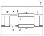
実施形態に係る光伝送装置は、半導体MZ光変調器10、光源17、駆動回路18を主要構成要素として備えた光送信機である。
The optical transmission apparatus according to the embodiment is an optical transmitter including the semiconductor MZ
この光伝送装置が備える光源17は、レーザー光を出力する半導体レーザー(ダイオードレーザー)である。半導体MZ光変調器10は、光源17からのレーザー光を変調する(パルス化する)ための光変調器(詳細は後述)である。
The
駆動回路18は、外部から与えられるデータに基づき、そのデータに応じた内容の光信号が半導体MZ光変調器10から出力されるように、半導体MZ光変調器10の各アーム11X(X=1,2)上の電極15に変調電圧を印加する回路である。この駆動回路18は、各アーム11X(電極15)に、各時刻における時間変化率の正負が逆の,振幅(電圧の変化範囲)が等しい変調電圧を印加する回路となっている。また、駆動回路18は、各アーム11Xを伝搬する光におよそ−π/4ラジアン〜+π/4ラジアンの位相変化が生じることになる変調電圧を各アーム11Xに印加する回路ともなっている。
The
半導体MZ光変調器10は、2本のアーム111及び112と、光分配器12と、光結合器13と、2つの電極15とを、備えた光変調器である。
The semiconductor MZ
光分配器12は、光源17からのレーザー光(以下、入力光と表記する)を、各アーム11Xへの2波に分けるためのデバイスである。この光分配器12は、入力光を、強度が等しい2波に分けて、各アーム11X(X=1,2)に供給するもの(本実施形態では、MMIカプラ)となっている。
アーム111、アーム112は、いずれも、半導体量子井戸構造を有する光導波路である。図示してあるように、半導体MZ光変調器10が備えるアーム111は、その一部に、損失調整部14(詳細は後述)を備えたものとなっている。なお、半導体MZ光変調器10が備える各光導波路(アーム11X、アーム11X以外の各光導波路)は、変調光波長において導波モードが単一となる幅を有するものである。
Each of the arms 11 1 and 11 2 is an optical waveguide having a semiconductor quantum well structure. As is shown, the arm 11 1 provided in the semiconductor MZ
光結合器13は、アーム111からの光とアーム112からの光とを干渉・合波させ、合波結果を図1における上側の光導波路に出力するデバイスである。半導体MZ光変調器10は、この光結合器13としても、MMIカプラが採用されたものとなっている。
The
電極15は、アーム11Xの一部の領域に電圧を印加するための電極である。図示してあるように、半導体MZ光変調器10の各電極15は、アーム11Xの一部の領域を覆う矩形電極に、駆動回路18からの信号線を接続するためのパッド15aを接続した形状のものとなっている。
損失調整部14は、他の部分(アーム111の損失調整部14以外の部分)よりも、量子井戸の層厚が厚くなるように形成した部分である。量子井戸の層厚を厚くすると、励起子吸収光波長が長波化し、その結果として、光吸収係数が大きくなる。従って、この損失調整部14は、他の部分よりも、光吸収係数が大きな部分となっていることになる。
半導体MZ光変調器10は、この損失調整部14の形状(主としてアーム111の長さ方向の長さ)を、オフ状態におけるアーム111(損失調整部14を含むアーム111全体)の損失(伝搬損失)とアーム112の損失とが一致するように定めたものとなっている。なお、オフ状態とは、出力光の強度が最小となる電圧が各アーム11X(電極15)に印加されている状態のことである。
The semiconductor MZ
また、半導体MZ光変調器10は、電圧が印加されていない状態にあるアーム111及び112から出力される光の位相差(以下、初期位相差と表記する)が、“π/2+2nπ”ラジアン(nは、整数)となるように設計・製造されたものともなっている。
The semiconductor MZ
次に、実施形態に係る光伝送装置に、上記構成を採用している理由を説明する。 Next, the reason why the above configuration is adopted in the optical transmission apparatus according to the embodiment will be described.
上記したように、実施形態に係る光伝送装置は、半導体MZ光変調器10の各アーム11Xに、各時刻における時間変化率の正負が逆の,振幅が等しい変調電圧を印加する駆動回路18を備えている。
As described above, in the optical transmission device according to the embodiment, the
光伝送装置に、そのような駆動回路18を採用しているのは、各時刻における時間変化率の正負が逆の,振幅が等しい変調電圧を各アーム11Xに印加すれば、半導体MZ光変調器10をチャープが少ない光変調器として機能させることが出来るためである。
Such a
すなわち、半導体MZ変調器10の各アーム11Xに、上記のように変化する変調電圧を印加した場合、図2に示してあるように、各アーム11Xにおける最大位相変化量Δφ1、Δφ2の絶対値が一致することになる。なお、最大位相変化量とは、出力光強度が最大となる電圧(図2における矢印の先端側の電圧)の印加によりアーム11Xを伝搬する光に生ずる,出力光強度が最小となる電圧(図2における矢印の根本側の電圧)印加時の位相を基準とした位相変化量のことである。
That is, when the modulation voltage changing as described above is applied to each arm 11 X of the
従って、各時刻における時間変化率の正負が逆の,振幅が等しい変調電圧を各アーム11Xに印加すれば(上記駆動回路18を採用しておけば)、半導体MZ光変調器10をチャープが少ない光変調器として機能させることが出来ることになる。
Thus, the positive and negative reverse time rate of change at each time, by applying an amplitude equal modulation voltages to the respective arm 11 X (if adopted the drive circuit 18), the chirp semiconductor MZ
ただし、既に説明したように、半導体MZ変調器は、各アームの損失が印加電圧によって比較的に大きく変化するもの(図11参照)となっている。そのため、上記内容の制御を既存構成の半導体MZ変調器に対して行った場合には、図3に示してあるように、オフ状態における各アームの損失α1、α2が大きく異なってしまい、その結果として、オフ状態における出力光の強度がさほど小さくならないことになる。 However, as already described, the semiconductor MZ modulator is such that the loss of each arm changes relatively greatly depending on the applied voltage (see FIG. 11). Therefore, when the above-described control is performed on the semiconductor MZ modulator having the existing configuration, as shown in FIG. 3, the losses α 1 and α 2 of each arm in the off state are greatly different. As a result, the intensity of the output light in the off state does not decrease so much.
半導体MZ変調器10のアーム111に、損失調整部14を設けているのは、この不具合が発生しないようにするためである。
The arm 11 1 of the
すなわち、アーム111に、“光吸収係数が他の部分よりも大きな、オフ状態におけるアーム111の損失とアーム112の損失とが一致するように、その形状を定めた損失調整部14”を設けておけば、図4に模式的に示したように、オフ状態における各アーム11X(図では、アームX)の損失α1、α2を一致させることが出来る。
That is, the arm 11 1 has a “
従って、損失調整部14がアーム111に設けられている半導体MZ光変調器10は、上記不具合が生じない光変調器(換言すれば、消光比が高い光変調器)として機能することになる。
Thus, the semiconductor MZ
また、損失調整部14を量子井戸の層厚調整により形成しているのは、そのようにしておけば、損失調整部14を簡単に実現(製造)できることになることに加え、両アーム間に、光波長に依存する損失差を付けることが可能になるからである。
In addition, the
具体的には、量子井戸の層厚調整以外の方法、例えば、両アームの形状を非対称にする(例えば、導波路幅を両アーム間で変える)といった方法や、バンドギャップ波長が長波になるように組成を変化させるといった方法によっても、半導体MZ光変調器の両アーム間に損失差をつけることができる。ただし、前者の方法により所望の損失差を有する2アームを製造するためには、導波路幅等を極めて高精度に制御しなければならない。そのため、両アームの形状を非対称にすることによって半導体MZ光変調器の両アーム間に損失
差を付けることは、非現実的である。
Specifically, a method other than adjusting the layer thickness of the quantum well, for example, a method of making the shapes of both arms asymmetric (for example, changing the waveguide width between both arms), or a band gap wavelength becomes a long wave. A loss difference can be provided between both arms of the semiconductor MZ optical modulator also by a method of changing the composition. However, in order to manufacture two arms having a desired loss difference by the former method, the waveguide width and the like must be controlled with extremely high accuracy. Therefore, it is unrealistic to provide a loss difference between both arms of the semiconductor MZ optical modulator by making the shapes of both arms asymmetric.
また、半導体MZ光変調器では、屈折率変化と吸収変化の関係自体に波長依存性がある。従って、半導体MZ光変調器を広い波長範囲に渡って使用する場合には、両アーム間の損失差についても波長依存性を持たせておかないと、波長毎にオフ状態の損失差を零とすることが出来ない。しかしながら、前者の方法は、両アーム間に、光波長に依存する損失差を付けることができないという欠点を有するものともなっている。 Further, in the semiconductor MZ optical modulator, the relationship between the refractive index change and the absorption change itself has wavelength dependency. Therefore, when the semiconductor MZ optical modulator is used over a wide wavelength range, the loss difference in the OFF state is set to zero for each wavelength unless the loss difference between the arms is also wavelength-dependent. I can't do it. However, the former method has a drawback that a loss difference depending on the optical wavelength cannot be provided between the arms.
一方、後者の方法によれば、両アーム間に光波長に依存する損失差を付けることができる。ただし、この方法を採用した場合、製造手順が複雑にならざるを得ないが、損失調整部14を量子井戸の層厚調整により形成するようにしておけば、マスクを用いた選択成長(詳細は後述)により、損失調整部14を簡単に実現できる。しかも、量子井戸の層厚調整によれば、両アーム間に、光波長に依存する損失差を付けることも可能である。そのため、損失調整部14を量子井戸の層厚調整により形成しているのである。
On the other hand, according to the latter method, it is possible to add a loss difference depending on the optical wavelength between the arms. However, when this method is adopted, the manufacturing procedure must be complicated. However, if the
さらに、アーム111及び112間の初期位相差を“π/2+2nπ”ラジアン(nは、整数)としておけば、図2に示したように、各アーム11xへの変調電圧の最大値と最
小値を揃えた駆動が出来るため、チャープ量を最小にすることが出来る。そのため、半導体MZ光変調器10を、アーム111及び112間の初期位相差が“π/2+2nπ”ラジアンであるものとした上で、駆動回路18として、各アーム11Xを伝搬する光に、−π/4ラジアン〜+π/4ラジアンの位相変化を生じさせる変調電圧を出力するものを採用しているのである。
Further, if the initial phase difference between the arms 11 1 and 11 2 is set to “π / 2 + 2nπ” radians (n is an integer), as shown in FIG. 2, the maximum value and the minimum value of the modulation voltage applied to each arm 11x. Since driving with uniform values can be performed, the amount of chirp can be minimized. Therefore, the semiconductor MZ
次に、本実施形態に係る半導体MZ変調器10の製造手順の一例を説明する。
Next, an example of a manufacturing procedure of the
上記した半導体MZ変調器10は、例えば、図5A〜図5Sに示した手順で製造できるものである。
The
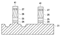
すなわち、この手順による半導体MZ変調器10の製造時には、まず(図5A参照)、n−InP基板21上に、CVD(Chemical Vapor Deposition:化学気相成長)法によ
りSiO2膜22が形成される。次いで、『SiO2膜22上へフォトレジストを塗布し、塗布したフォトレジストを露光し、露光したフォトレジストを現像する』といった手順で、SiO2膜22上に所定形状(詳細は後述)のレジストパターン40が形成される。
That is, when the
そして、レジストパターン40をマスクとしてSiO2膜22がBHF(Buffered HF
)等によりウェットエッチングされる。その後、レジストパターン40が除去されることにより、n−InP基板21上に、図5B、図5Cに示したような形状の2つの選択成長マスク領域23(SiO2膜22の一部)が設けられている構造が製造される。
Then, the SiO 2 film 22 is formed with BHF (Buffered HF) using the resist
) Or the like. Thereafter, by removing the resist
なお、各選択成長マスク領域23(以下、マスク領域23とも表記する)の形状及び位置(レジストパターン40の形状)は、さまざまなことを考慮して決定しておく。 The shape and position of each selective growth mask region 23 (hereinafter also referred to as mask region 23) (the shape of the resist pattern 40) are determined in consideration of various things.
具体的には、各マスク領域23の幅Wm、マスク領域23間の間隙幅Wgは、2つのマスク領域23に挟まれた領域(以下、“高成長速度領域”と表記する)内の活性層成長速度(平均的なもの:以下、同様)の,他領域における活性層成長速度に対する比が、所望の値(例えば、1.2)となるように決定しておく。また、各マスク領域23の長さLmは、その後に形成されるアーム111の損失と、アーム112の損失とが、オフ状態において一致する長さ(例えば500μm)となるように、活性層組成、井戸層厚、駆動条件等から決定しておく。
Specifically, the width Wm of each
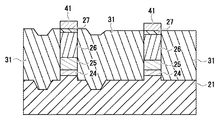
マスク領域23の形成後には、n−InP基板21のマスク領域23が形成されている側の面上に、MOCVD(Metal Organic Chemical Vapor Deposition:有機金属気相成
長法)により、100nm程度の厚さの,n型のInPバッファ層24が積層される(図5D)。次いで、そのInPバッファ層24上に、InGaAsP−井戸とInP−障壁から成るMQW(Multi-Quantum Wells:多重量子井戸)層25が形成される。
After the
なお、QCSEによって実用上十分な大きさの屈折率変化を得るには、MQW層25のバンド端遷移波長と入力光波長とが近いことが望ましい。ただし、入力光波長がバンド端遷移波長に近すぎると吸収の影響も大きくなる。そのため、入力光波長を1.55μm付近とする場合には、バンド端遷移波長が1.4μm程度となるように、MQW層25の組
成(例えば、In(0.6)Ga(0.4)As(0.85)P(0.15))と層厚(例えば10nm)とを決定しておくことが望ましい。この時、上記高成長速度領域では、成長速度比に応じてMQW層厚が大きく(ここでは12nmに)なる。
In order to obtain a practically sufficient refractive index change by QCSE, it is desirable that the band edge transition wavelength of the
MQW層25の形成後には、マスク領域23が、BHF等によりウェットエッチングされる。その後、MOCVD法により、p型のInPクラッド層26と、p型のInGaAsコンタクト層27とが、形成される(図5E)。
After the formation of the
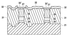
次いで、マスク領域23形成時と同様の手順で、導波路形成用の,Si02からなるマスクパターン41が形成される(図5F)。そして、形成したマスクパターン41をマスクとした、RIE(Reactive Ion Etching)によるドライエッチングが行われることにより、n−InP基板21上にメサストライプが形成される(図5G)。
Then, the same procedure as when the
なお、上記工程中で形成されるマスクパターン41は、図5Hに示したような形状を有するものである。ただし、上記工程中で実際に形成されるマスクパターン41は、それをマスクとしたドライエッチングによって、図1を用いて既に説明した機能・構成を有する光分配器12、アーム11X等が得られるように、その形状が設計されたものである。
Note that the
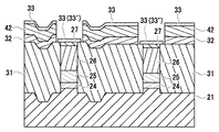
メサストライプの形成が完了した場合には、MOCVD法によって、メサストライプ周囲に、SI(Semi-Insulated:高抵抗)−InP層31(図5I)を成長させてから、マスクパターン41が除去される(図5J)。そして、『InGaAsコンタクト層27上へのレジストマスクの形成工程』等を含む一連の工程により、InGaAsコンタクト層27の,Au/Zn/Au電極33′を形成する部分以外の部分がウェットエッチングされる(図5K)。なお、Au/Zn/Au電極33′とは、各アーム11X(InPバッファ層24、MQW層25等が積層されたストライプ状部分)の電圧を印加する部分上に形成される,電極15の一部を成す電極(図5O参照)のことである。
When the formation of the mesa stripe is completed, the
InGaAsコンタクト層27のパターニング後には、一連の工程を経たn−InP基板21の,SI−InP層31が形成されている側の全面に、CVD法によりSiO2膜32(図5L参照)が形成される。
After patterning the
次いで、Au/Zn/Au電極33′を形成する部分が開口部42aとなっているレジストマスク42(図5M参照)が、SiO2膜32上に形成される。
Next, a resist mask 42 (see FIG. 5M) in which a portion where the Au / Zn /
レジストマスク42の形成後には、そのレジストマスク42をマスクとしたエッチングにより、SiO2膜32の,Au/Zn/Au電極33′を形成する部分上の部分が除去される(図5L、図5M)。その後、真空蒸着法により、Au/Zn/Au膜33が形成される(図5N)。そして、レジストマスク42を、その上に形成されているAu/Zn/Au膜33と共に除去することにより、各アーム11X上に、Au/Zn/Au電極33′が存在する構造(図5O、図5P)が製造される。
After the formation of the resist
その後、図5Rに示してあるような形状のAu電極34を形成するためのレジストマスク44が形成される(図5Q)。そして、メッキにより、Au電極34が形成されてから(Au電極34とAu/Zn/Au電極33′とからなる電極15(図1参照)が形成されてから)、レジストマスク44が除去される(図5R)。
Thereafter, a resist
レジストマスク44の除去後には、裏面電極37が形成される(図5S)。この裏面電極37は、通常、AuGe/Au膜35を蒸着してから、Auメッキ層36を形成するといった手順で形成される。
After removing the resist
このような手順を採用しておけば、変調電圧の中心バイアスが−3V程度、変調振幅(全幅)が2V程度の変調電圧により駆動できる、オフ状態における両アーム111、112間のQCSEによる過剰損失差(図3におけるα2−α1)が、例えば、0.5dBである半導体MZ光変調器10であって、それと同じ伝搬損失が発生する損失調整部14を備えているが故に、消光比が高い半導体MZ光変調器10を、容易且つ確実に製造できることになる。
If such a procedure is employed, the QCSE between the arms 11 1 and 11 2 in the off state can be driven by the modulation voltage having a modulation voltage center bias of about −3 V and a modulation amplitude (full width) of about 2 V. Since the excess loss difference (α 2 −α 1 in FIG. 3) is, for example, the semiconductor MZ
《変形形態》
上記した光伝送装置は、各種の変形を行うことが出来るものである。例えば、光伝送装置を、図6に示した構成を有する半導体MZ光変調器10を備えた装置、すなわち、光分配器12及び光結合器13として、MMIカプラではなく、Y分岐導波路が使用されている半導体MZ光変調器10を備えた装置に変形することが出来る。また、光伝送装置を、光分配器12及び光結合器13として、方向性結合器が使用されている半導体MZ光変調器10を備えた装置に変形することも出来る。
<Deformation>
The optical transmission apparatus described above can be variously modified. For example, the optical transmission device is a device including the semiconductor MZ
また、初期位相差が“π/2+2nπ”ラジアン(nは、整数)となるように、アーム111及びアーム112を設計するのではなく、アーム112及び/又はアーム111に、初期位相差を調整(制御)するための位相調整機構を設けておくことも出来る。そのような位相調整機構としては、電圧印加による屈折率変化を利用して位相を調整する機構、電流注入による自由キャリア密度の変化に伴う屈折率変化を利用して位相を調整する機構、温度変化に伴う屈折率変化を利用して位相を調整する機構が考えられる。ただし、電圧/電流を利用する機構は、屈折率変化に伴い吸収の変化が起こるため、制御が難しいものとなる。従って、半導体MZ光変調器10に位相調整機構を実装する場合には、図7に示したように、半導体MZ光変調器10のアーム112上(又は、アーム111上)にヒータ電極19を設けておくことが好ましい。
In addition, the arm 11 1 and the arm 11 2 are not designed so that the initial phase difference is “π / 2 + 2nπ” radians (n is an integer), but the initial position is set in the arm 11 2 and / or the arm 11 1. A phase adjustment mechanism for adjusting (controlling) the phase difference can also be provided. Such a phase adjustment mechanism includes a mechanism that adjusts the phase by using a change in refractive index due to voltage application, a mechanism that adjusts the phase by using a change in refractive index due to a change in free carrier density due to current injection, and a temperature change. A mechanism for adjusting the phase by using a change in refractive index accompanying the above can be considered. However, the mechanism using the voltage / current is difficult to control because a change in absorption occurs with a change in refractive index. Therefore, a semiconductor when implementing the phase adjustment mechanism to the MZ
また、損失調整部14は、“光吸収係数が他の部分よりも大きな、オフ状態におけるアーム111の損失とアーム112の損失とが一致するように、その形状を定めた”ものでありさえすれば良い。従って、形成後の損失調整部14(半導体MZ光変調器10が備える損失調整部14)が、実際に、オフ状態におけるアーム111の損失とアーム112の損失とを完全に一致させるものとなっている必要はない。
Further, the
また、損失調整部14を、電極15下に設けておくことも出来る。ただし、そのような構成を採用した場合、損失調整部14のサイズを決定するのが困難になる。そのため、損失調整部14は、上記した半導体MZ光変調器10のように、電極15下ではない部分に設けておくことが望ましい。
Further, the
半導体MZ光変調器10を、InGaAsP/InP量子井戸以外の活性層を備えたもの(例えば、Zn,Cd,Hg,Al,N,Sb,S,Te等のII,III,V,VI族元
素からなる混晶を活性層としたもの)に変形することも出来る。また、半導体MZ光変調
器10を、双方のアーム111及び112に、それぞれ、損失調整部14相当のものが設けられているもの(オフ状態における両アーム111及び112間の損失が一致するように、各アーム11Xで損失が調整される構成を有するもの)に変形することも出来る。
Semiconductor MZ
半導体MZ光変調器10を、上記構造(SI−BH構造)とは異なる構造の導波路(例えば、PNPN型の埋め込み導波路や、半導体での埋め込みを行わないハイメサ型導波路)を備えたものに変形することも出来る。さらに、半導体MZ光変調器10の光結合器13を、合波した光の何%かを図1における下側の光導波路に出力するものとしておいても良いことや、光伝送装置を、光中継器に変形しても良いことなどは、当然のことである。
The semiconductor MZ
以上、開示した技術に関し、更に以下の付記を開示する。 As described above, the following additional notes are disclosed with respect to the disclosed technology.
(付記1) マッハツェンダ干渉計を成す,半導体量子井戸構造を有する第1及び第2の光導波路と、
前記第1の光導波路に電圧を印加するための第1電極と、
前記第2の光導波路に電圧を印加するための第2電極と、
を備え、
前記第1の光導波路及び前記第2の光導波路の少なくとも一方の光導波路の一部に、その光吸収係数が当該光導波路の他の部分に比べて大きな損失調整部であって、出力光の強度が最小となる電圧を前記第1電極及び前記第2電極に印加した場合における前記第1の光導波路の伝搬損失と前記第2の光導波路の伝搬損失とが一致するように、その形状が定められた損失調整部が、設けられている
ことを特徴とする半導体マッハツェンダ型光変調器。
(Additional remark 1) The 1st and 2nd optical waveguide which has a semiconductor quantum well structure which comprises a Mach-Zehnder interferometer,
A first electrode for applying a voltage to the first optical waveguide;
A second electrode for applying a voltage to the second optical waveguide;
With
A part of at least one of the first optical waveguide and the second optical waveguide is a loss adjustment unit having a light absorption coefficient larger than that of the other part of the optical waveguide, The shape is such that the propagation loss of the first optical waveguide coincides with the propagation loss of the second optical waveguide when a voltage having a minimum intensity is applied to the first electrode and the second electrode. A semiconductor Mach-Zehnder type optical modulator, characterized in that a predetermined loss adjusting unit is provided.
(付記2) 前記損失調整部が、
前記光導波路の前記他の部分の量子井戸よりも層厚が厚い量子井戸である
ことを特徴とする付記1に記載の半導体マッハツェンダ型光変調器。
(Supplementary Note 2) The loss adjustment unit is
The semiconductor Mach-Zehnder optical modulator according to
(付記3) 前記第1の光導波路及び前記第2の光導波路の少なくとも一方が、
前記損失調整部として機能する部分を含む、光伝播方向に沿って連続的に厚みの変化する量子井戸構造を有する光導波路である
ことを特徴とする付記1に記載の半導体マッハツェンダ型光変調器。
(Appendix 3) At least one of the first optical waveguide and the second optical waveguide is
The semiconductor Mach-Zehnder optical modulator according to
(付記4) 前記第1の光導波路と前記第2の光導波路との間の初期位相差が、π/2+2nπ(nは、整数)ラジアンである
ことを特徴とする付記1乃至付記3のいずれか一項に記載の半導体マッハツェンダ型光変調器。
(Supplementary note 4) Any of
(付記5) 第1の光導波路と前記第2の光導波路との間の初期位相差を調整するための位相調整機構を、さらに、備える
ことを特徴とする付記1乃至付記3のいずれか一項に記載の半導体マッハツェンダ型光変調器。
(Supplementary Note 5) Any one of
(付記6) 前記損失調整部が、
前記第1の光伝送路の前記第1電極により覆われていない部分、又は、前記第2の光伝送路の前記第2電極により覆われていない部分に設けられている
ことを特徴とする付記1乃至付記5のいずれか一項に記載の半導体マッハツェンダ型光変調器。
(Additional remark 6) The said loss adjustment part is
Note that the first optical transmission line is provided in a portion that is not covered by the first electrode, or a portion that is not covered by the second electrode in the second optical transmission line. The semiconductor Mach-Zehnder optical modulator according to any one of 1 to Appendix 5.
(付記7) 付記1乃至付記6のいずれか一項に記載の半導体マッハツェンダ型光変調
器と、
前記半導体マッハツェンダ型光変調器の前記第1電極と前記第2電極とに、同時刻における時間変化率の正負が逆の,振幅が等しい変調電圧を印加することによって、前記半導体マッハツェンダ型光変調器を駆動する駆動回路と、
を備えることを特徴とする光伝送装置。
(Supplementary note 7) The semiconductor Mach-Zehnder optical modulator according to any one of
The semiconductor Mach-Zehnder optical modulator is applied with a modulation voltage having the same amplitude but opposite amplitude of the time change rate at the same time, to the first electrode and the second electrode of the semiconductor Mach-Zehnder optical modulator. A drive circuit for driving
An optical transmission device comprising:
(付記8) 半導体基板上に、マッハツェンダ干渉計を成す,半導体量子井戸構造を有する第1及び第2の光導波路を形成する光導波路形成工程と、
前記第1の光導波路及び前記第2の光導波路の少なくとも一方の光導波路の一部に、その光吸収係数が当該光導波路の他の部分に比べて大きな損失調整部であって、出力光の強度が最小となる電圧を前記第1電極及び前記第2電極に印加した場合における前記第1の光導波路の伝搬損失と前記第2の光導波路の伝搬損失とが一致するように、その形状が定められた損失調整部を形成する損失調整部形成工程と、
を含むことを特徴とする半導体マッハツェンダ型光変調器の製造方法。
(Additional remark 8) The optical waveguide formation process which forms the 1st and 2nd optical waveguide which has a semiconductor quantum well structure which comprises a Mach-Zehnder interferometer on a semiconductor substrate,
A part of at least one of the first optical waveguide and the second optical waveguide is a loss adjustment unit having a light absorption coefficient larger than that of the other part of the optical waveguide, The shape is such that the propagation loss of the first optical waveguide coincides with the propagation loss of the second optical waveguide when a voltage having a minimum intensity is applied to the first electrode and the second electrode. A loss adjusting part forming step for forming a defined loss adjusting part;
A method of manufacturing a semiconductor Mach-Zehnder type optical modulator.
(付記9) 前記半導体基板の前記損失調整部を形成すべき部分の近傍に,前記第1及び前記第2の光導波路の量子井戸の構成材料がその上に積層されないマスクを形成する工程を、さらに、含み、
前記光導波路形成工程及び前記損失調整部形成工程として、
前記量子井戸の構成材料を堆積させることにより、前記マスクが形成された前記半導体基板上に、少なくとも一方の光導波路の一部に、前記損失調整部として機能する,他の部分の量子井戸よりも層厚が厚い部分が存在する、マッハツェンダ干渉計を成す,半導体量子井戸構造を有する第1及び第2の光導波路を形成する工程が行われる
ことを特徴とする付記8に記載の半導体マッハツェンダ型光変調器の製造方法。
(Additional remark 9) The process of forming the mask in which the constituent material of the quantum well of the said 1st and 2nd optical waveguide is not laminated | stacked on the vicinity of the part which should form the said loss adjustment part of the said semiconductor substrate, In addition,
As the optical waveguide forming step and the loss adjusting portion forming step,
By depositing the constituent material of the quantum well, on the semiconductor substrate on which the mask is formed, a part of at least one of the optical waveguides functions as the loss adjusting unit, as compared to the other part of the quantum well. 9. The semiconductor Mach-Zehnder type light according to appendix 8, wherein a step of forming first and second optical waveguides having a semiconductor quantum well structure, which forms a Mach-Zehnder interferometer, in which a thick layer portion exists is performed. Modulator manufacturing method.
(付記10) 半導体マッハツェンダ型光変調器の駆動方法であって、
前記半導体マッハツェンダ型光変調器の,マッハツェンダ干渉計を成している2本の光導波路に、同時刻における時間変化率の正負が逆の,振幅が等しい変調電圧を印加することによって、前記半導体マッハツェンダ型光変調器を駆動する
ことを特徴とする半導体マッハツェンダ型光変調器の駆動方法。
(Supplementary Note 10) A method of driving a semiconductor Mach-Zehnder optical modulator,
The semiconductor Mach-Zehnder optical modulator is configured to apply a modulation voltage having the same amplitude and opposite amplitudes to the two optical waveguides constituting the Mach-Zehnder interferometer at the same time. A method for driving a semiconductor Mach-Zehnder optical modulator, comprising: driving a type optical modulator.
(付記11) 前記半導体マッハツェンダ型光変調器が、
出力光の強度が最小となる電圧を各光導波路に印加した場合における両光導波路の伝搬損失が等しい変調器である
ことを特徴とする付記10に記載の半導体マッハツェンダ型光変調器の駆動方法。
(Supplementary Note 11) The semiconductor Mach-Zehnder optical modulator includes:
11. The method of driving a semiconductor Mach-Zehnder optical modulator according to
10 半導体MZ光変調器
111,112 アーム
12 光分配器
13 光結合器
14 損失調整部
15 電極
15a パッド
17 光源
18 駆動回路
19 ヒータ電極
21 n−InP基板
22,32 SiO2膜
23 選択成長マスク領域
24 InPバッファ層
25 MQW層
26 InPクラッド層
27 InGaAsコンタクト層
31 SI−InP層
33 Au/Zn/Au電極
34 Au電極
35 AuGe/Au膜
36 Auメッキ層
37 裏面電極
40 レジストパターン
41 マスクパターン
42,44 レジストマスク
42a 開口部
DESCRIPTION OF
Claims (8)
前記第1の光導波路に電圧を印加するための第1電極と、
前記第2の光導波路に電圧を印加するための第2電極と、
を備え、
前記第1の光導波路及び前記第2の光導波路の少なくとも一方の光導波路の一部に、その光吸収係数が当該光導波路の他の部分に比べて大きな損失調整部であって、出力光の強度が最小となる電圧を前記第1電極及び前記第2電極に印加した場合における前記第1の光導波路の伝搬損失と前記第2の光導波路の伝搬損失とが一致するように、その形状が定められた損失調整部が、設けられている
ことを特徴とする半導体マッハツェンダ型光変調器。 First and second optical waveguides having a semiconductor quantum well structure forming a Mach-Zehnder interferometer;
A first electrode for applying a voltage to the first optical waveguide;
A second electrode for applying a voltage to the second optical waveguide;
With
A part of at least one of the first optical waveguide and the second optical waveguide is a loss adjustment unit having a light absorption coefficient larger than that of the other part of the optical waveguide, The shape is such that the propagation loss of the first optical waveguide coincides with the propagation loss of the second optical waveguide when a voltage having a minimum intensity is applied to the first electrode and the second electrode. A semiconductor Mach-Zehnder type optical modulator, characterized in that a predetermined loss adjusting unit is provided.
前記光導波路の前記他の部分の量子井戸よりも層厚が厚い量子井戸である
ことを特徴とする請求項1記載の半導体マッハツェンダ型光変調器。 The loss adjusting unit is
2. The semiconductor Mach-Zehnder optical modulator according to claim 1, wherein the semiconductor Mach-Zehnder optical modulator has a layer thickness larger than that of the quantum well of the other portion of the optical waveguide.
前記損失調整部として機能する部分を含む、光伝播方向に沿って連続的に厚みの変化する量子井戸構造を有する光導波路である
ことを特徴とする請求項1記載の半導体マッハツェンダ型光変調器。 At least one of the first optical waveguide and the second optical waveguide is
2. The semiconductor Mach-Zehnder optical modulator according to claim 1, wherein the semiconductor Mach-Zehnder optical modulator includes a quantum well structure including a portion functioning as the loss adjusting unit and having a thickness that continuously changes along a light propagation direction.
ことを特徴とする請求項1乃至請求項3のいずれか一項に記載の半導体マッハツェンダ型光変調器。 4. The initial phase difference between the first optical waveguide and the second optical waveguide is π / 2 + 2nπ (where n is an integer) radians. 5. The semiconductor Mach-Zehnder optical modulator according to the item.
前記半導体マッハツェンダ型光変調器の前記第1電極と前記第2電極とに、同時刻における時間変化率の正負が逆の,振幅が等しい変調電圧を印加することによって、前記半導
体マッハツェンダ型光変調器を駆動する駆動回路と、
を備えることを特徴とする光伝送装置。 A semiconductor Mach-Zehnder optical modulator according to any one of claims 1 to 4,
The semiconductor Mach-Zehnder optical modulator is applied with a modulation voltage having the same amplitude but opposite amplitude of the time change rate at the same time, to the first electrode and the second electrode of the semiconductor Mach-Zehnder optical modulator. A drive circuit for driving
An optical transmission device comprising:
前記第1の光導波路及び前記第2の光導波路の少なくとも一方の光導波路の一部に、その光吸収係数が当該光導波路の他の部分に比べて大きな損失調整部であって、出力光の強度が最小となる電圧を前記第1電極及び前記第2電極に印加した場合における前記第1の光導波路の伝搬損失と前記第2の光導波路の伝搬損失とが一致するように、その形状が定められた損失調整部を形成する損失調整部形成工程と、
を含むことを特徴とする半導体マッハツェンダ型光変調器の製造方法。 An optical waveguide forming step of forming first and second optical waveguides having a semiconductor quantum well structure, which forms a Mach-Zehnder interferometer on a semiconductor substrate;
A part of at least one of the first optical waveguide and the second optical waveguide is a loss adjustment unit having a light absorption coefficient larger than that of the other part of the optical waveguide, The shape is such that the propagation loss of the first optical waveguide coincides with the propagation loss of the second optical waveguide when a voltage having a minimum intensity is applied to the first electrode and the second electrode. A loss adjusting part forming step for forming a defined loss adjusting part;
A method of manufacturing a semiconductor Mach-Zehnder type optical modulator.
ことを特徴とする請求項7に記載の半導体マッハツェンダ型光変調器の製造方法。 Providing a mask in which the constituent material of the quantum well is not stacked thereon in the vicinity of the portion where the loss adjusting portion of the semiconductor substrate is to be formed, and then depositing the constituent material of the quantum well on the semiconductor substrate, The method of manufacturing a semiconductor Mach-Zehnder type optical modulator according to claim 7, further comprising a step of forming the layer so that the layer thickness is larger than that of the quantum well in the portion.
前記第1の光導波路に電圧を印加するための第1電極と、
前記第2の光導波路に電圧を印加するための第2電極と、
を備え、
前記第1の光導波路及び前記第2の光導波路の少なくとも一方の光導波路の一部に、その光吸収係数が当該光導波路の他の部分に比べて大きな損失調整部であって、出力光の強度が最小となる電圧を前記第1電極及び前記第2電極に印加した場合における前記第1の光導波路の伝搬損失と前記第2の光導波路の伝搬損失とが一致するように、その形状が定められた損失調整部が、設けられている
ことを特徴とする半導体マッハツェンダ型光変調器の駆動方法であって、
前記半導体マッハツェンダ型光変調器の,マッハツェンダ干渉計を成している前記第1及び第2の2つの光導波路に、同時刻における時間変化率の正負が逆の,振幅が等しい変調電圧を印加することによって、前記半導体マッハツェンダ型光変調器を駆動する
ことを特徴とする半導体マッハツェンダ型光変調器の駆動方法。 First and second optical waveguides having a semiconductor quantum well structure forming a Mach-Zehnder interferometer;
A first electrode for applying a voltage to the first optical waveguide;
A second electrode for applying a voltage to the second optical waveguide;
With
A part of at least one of the first optical waveguide and the second optical waveguide is a loss adjustment unit having a light absorption coefficient larger than that of the other part of the optical waveguide, The shape is such that the propagation loss of the first optical waveguide coincides with the propagation loss of the second optical waveguide when a voltage having a minimum intensity is applied to the first electrode and the second electrode. A specified loss adjustment section is provided.
A method of driving a semiconductor Mach-Zehnder type optical modulator, characterized in that
A modulation voltage having the same amplitude and opposite amplitude of the time change rate at the same time is applied to the first and second optical waveguides constituting the Mach-Zehnder interferometer of the semiconductor Mach-Zehnder type optical modulator. Thus, the semiconductor Mach-Zehnder optical modulator is driven. A method for driving a semiconductor Mach-Zehnder optical modulator.
Priority Applications (1)
| Application Number | Priority Date | Filing Date | Title |
|---|---|---|---|
| JP2010049325A JP5458964B2 (en) | 2010-03-05 | 2010-03-05 | Semiconductor Mach-Zehnder optical modulator, optical transmission device, method for manufacturing semiconductor Mach-Zehnder optical modulator, and method for driving semiconductor Mach-Zehnder optical modulator |
Applications Claiming Priority (1)
| Application Number | Priority Date | Filing Date | Title |
|---|---|---|---|
| JP2010049325A JP5458964B2 (en) | 2010-03-05 | 2010-03-05 | Semiconductor Mach-Zehnder optical modulator, optical transmission device, method for manufacturing semiconductor Mach-Zehnder optical modulator, and method for driving semiconductor Mach-Zehnder optical modulator |
Publications (2)
| Publication Number | Publication Date |
|---|---|
| JP2011186057A JP2011186057A (en) | 2011-09-22 |
| JP5458964B2 true JP5458964B2 (en) | 2014-04-02 |
Family
ID=44792444
Family Applications (1)
| Application Number | Title | Priority Date | Filing Date |
|---|---|---|---|
| JP2010049325A Expired - Fee Related JP5458964B2 (en) | 2010-03-05 | 2010-03-05 | Semiconductor Mach-Zehnder optical modulator, optical transmission device, method for manufacturing semiconductor Mach-Zehnder optical modulator, and method for driving semiconductor Mach-Zehnder optical modulator |
Country Status (1)
| Country | Link |
|---|---|
| JP (1) | JP5458964B2 (en) |
Families Citing this family (2)
| Publication number | Priority date | Publication date | Assignee | Title |
|---|---|---|---|---|
| JP2014191218A (en) * | 2013-03-27 | 2014-10-06 | Nippon Telegr & Teleph Corp <Ntt> | Optical modulator |
| JP6317294B2 (en) * | 2015-04-30 | 2018-04-25 | 日本電信電話株式会社 | Optical modulator driving voltage setting method and optical modulator with driving voltage set |
Family Cites Families (10)
| Publication number | Priority date | Publication date | Assignee | Title |
|---|---|---|---|---|
| JPH08146365A (en) * | 1994-11-16 | 1996-06-07 | Nec Corp | Semiconductor mach-zehnder modulation device and its production |
| GB2302738B (en) * | 1995-06-28 | 1999-03-03 | Northern Telecom Ltd | Semiconductor modulator with a shift |
| JPH0961766A (en) * | 1995-08-19 | 1997-03-07 | Nec Corp | Semiconductor optical modulator |
| JP2792482B2 (en) * | 1995-09-28 | 1998-09-03 | 日本電気株式会社 | Semiconductor Mach-Zehnder modulator |
| JP2993925B2 (en) * | 1997-07-14 | 1999-12-27 | 日本電信電話株式会社 | Light modulation element |
| JP2000066156A (en) * | 1998-08-25 | 2000-03-03 | Mitsubishi Electric Corp | Mach-zehunder type optical modulator |
| JP2000089181A (en) * | 1998-09-14 | 2000-03-31 | Nippon Telegr & Teleph Corp <Ntt> | Semiconductor optical modulation device |
| JP2006259600A (en) * | 2005-03-18 | 2006-09-28 | Furukawa Electric Co Ltd:The | Interference type optical signal processor |
| JP2009204884A (en) * | 2008-02-28 | 2009-09-10 | Oki Semiconductor Co Ltd | Light modulating device |
| JP2010008763A (en) * | 2008-06-27 | 2010-01-14 | Mitsubishi Electric Corp | Optical modulation device and optical semiconductor device |
-
2010
- 2010-03-05 JP JP2010049325A patent/JP5458964B2/en not_active Expired - Fee Related
Also Published As
| Publication number | Publication date |
|---|---|
| JP2011186057A (en) | 2011-09-22 |
Similar Documents
| Publication | Publication Date | Title |
|---|---|---|
| EP0809129B1 (en) | Semiconductor optical modulator and method for making the same | |
| JP2867995B2 (en) | Semiconductor Mach-Zehnder modulator and manufacturing method thereof | |
| EP2458433B1 (en) | Optical modulator and manufacturing method of the optical modulator | |
| US8620115B2 (en) | Optical modulators with controllable chirp | |
| US11281067B2 (en) | Transparent conducting oxide (TCO) based integrated modulators | |
| JP4235154B2 (en) | Semiconductor Mach-Zehnder type optical modulator and manufacturing method thereof | |
| US20130108204A1 (en) | Optical modulation device, driving method of optical modulation device, and manufacturing method of optical modulation device | |
| US5655034A (en) | Mach-Zehnder type modulator and method of driving the same | |
| GB2302738A (en) | Mach Zehnder modulator | |
| US6222966B1 (en) | Adiabatic Y-branch waveguide having controllable chirp | |
| EP1602963B1 (en) | Semiconductor optical modulator | |
| US5757985A (en) | Semiconductor mach-zehnder-type optical modulator | |
| US20090220185A1 (en) | Light modulating device | |
| Dogru et al. | 0.2 v drive voltage substrate removed electro-optic Mach–Zehnder modulators with MQW cores at 1.55 μm | |
| JP5458964B2 (en) | Semiconductor Mach-Zehnder optical modulator, optical transmission device, method for manufacturing semiconductor Mach-Zehnder optical modulator, and method for driving semiconductor Mach-Zehnder optical modulator | |
| US9298024B2 (en) | Semiconductor Mach-Zender modulator and method to drive the same | |
| JPH07191290A (en) | Semiconductor mach-zehnder modulator and its production | |
| US6115169A (en) | Semiconductor optical modulator and integrated optical circuit device | |
| Yao et al. | Multi-Parameter Optimization of a Shallow Ridge InP Traveling Wave Mach-Zehnder Modulator for Beyond 200 Gb/s Optical Datacom Applications | |
| US20040201008A1 (en) | In-phase RF drive of Mach-Zehnder modulator push-pull electrodes by using coupled quantum well optical active region | |
| WO2024062518A1 (en) | Mach-zehnder-type optical modulator and optical transmission device | |
| JPH0353225A (en) | Semiconductor optical modulator | |
| JPH09101491A (en) | Semiconductor mach-zehnder modulator and its production | |
| US20050141072A1 (en) | Electroabsorption modulator with two sections | |
| Tsuzuki et al. | Low driving voltage 40 Gbit/s nin Mach-Zehnder modulator fabricated on InP substrate |
Legal Events
| Date | Code | Title | Description |
|---|---|---|---|
| A621 | Written request for application examination |
Free format text: JAPANESE INTERMEDIATE CODE: A621 Effective date: 20130108 |
|
| A977 | Report on retrieval |
Free format text: JAPANESE INTERMEDIATE CODE: A971007 Effective date: 20130924 |
|
| A131 | Notification of reasons for refusal |
Free format text: JAPANESE INTERMEDIATE CODE: A131 Effective date: 20131001 |
|
| A521 | Request for written amendment filed |
Free format text: JAPANESE INTERMEDIATE CODE: A523 Effective date: 20131202 |
|
| TRDD | Decision of grant or rejection written | ||
| A01 | Written decision to grant a patent or to grant a registration (utility model) |
Free format text: JAPANESE INTERMEDIATE CODE: A01 Effective date: 20131217 |
|
| A61 | First payment of annual fees (during grant procedure) |
Free format text: JAPANESE INTERMEDIATE CODE: A61 Effective date: 20131230 |
|
| R150 | Certificate of patent or registration of utility model |
Ref document number: 5458964 Country of ref document: JP Free format text: JAPANESE INTERMEDIATE CODE: R150 Free format text: JAPANESE INTERMEDIATE CODE: R150 |
|
| LAPS | Cancellation because of no payment of annual fees |