JP5451098B2 - Manufacturing method of semiconductor device - Google Patents
Manufacturing method of semiconductor device Download PDFInfo
- Publication number
- JP5451098B2 JP5451098B2 JP2009026702A JP2009026702A JP5451098B2 JP 5451098 B2 JP5451098 B2 JP 5451098B2 JP 2009026702 A JP2009026702 A JP 2009026702A JP 2009026702 A JP2009026702 A JP 2009026702A JP 5451098 B2 JP5451098 B2 JP 5451098B2
- Authority
- JP
- Japan
- Prior art keywords
- conductivity type
- type region
- region
- impurities
- forming
- Prior art date
- Legal status (The legal status is an assumption and is not a legal conclusion. Google has not performed a legal analysis and makes no representation as to the accuracy of the status listed.)
- Expired - Fee Related
Links
- 239000004065 semiconductor Substances 0.000 title claims description 32
- 238000004519 manufacturing process Methods 0.000 title claims description 24
- 239000012535 impurity Substances 0.000 claims description 59
- 238000009792 diffusion process Methods 0.000 claims description 58
- 230000003321 amplification Effects 0.000 claims description 32
- 238000003199 nucleic acid amplification method Methods 0.000 claims description 32
- 238000000034 method Methods 0.000 claims description 21
- 238000002513 implantation Methods 0.000 claims description 13
- 238000006243 chemical reaction Methods 0.000 claims description 12
- 239000004020 conductor Substances 0.000 claims description 5
- 238000002347 injection Methods 0.000 claims description 5
- 239000007924 injection Substances 0.000 claims description 5
- 230000004888 barrier function Effects 0.000 claims description 4
- 229910052751 metal Inorganic materials 0.000 claims description 3
- 239000002184 metal Substances 0.000 claims description 3
- 238000003384 imaging method Methods 0.000 description 36
- OAICVXFJPJFONN-UHFFFAOYSA-N Phosphorus Chemical compound [P] OAICVXFJPJFONN-UHFFFAOYSA-N 0.000 description 17
- 229910052698 phosphorus Inorganic materials 0.000 description 17
- 239000011574 phosphorus Substances 0.000 description 17
- 239000000758 substrate Substances 0.000 description 15
- 239000010410 layer Substances 0.000 description 13
- 229910052785 arsenic Inorganic materials 0.000 description 12
- RQNWIZPPADIBDY-UHFFFAOYSA-N arsenic atom Chemical compound [As] RQNWIZPPADIBDY-UHFFFAOYSA-N 0.000 description 12
- 238000002955 isolation Methods 0.000 description 11
- XUIMIQQOPSSXEZ-UHFFFAOYSA-N Silicon Chemical compound [Si] XUIMIQQOPSSXEZ-UHFFFAOYSA-N 0.000 description 10
- 230000008569 process Effects 0.000 description 10
- 229910052710 silicon Inorganic materials 0.000 description 10
- 239000010703 silicon Substances 0.000 description 10
- 238000010586 diagram Methods 0.000 description 8
- 238000005036 potential barrier Methods 0.000 description 8
- 230000015572 biosynthetic process Effects 0.000 description 5
- 229910021420 polycrystalline silicon Inorganic materials 0.000 description 5
- 229920005591 polysilicon Polymers 0.000 description 5
- 230000010354 integration Effects 0.000 description 4
- ZOXJGFHDIHLPTG-UHFFFAOYSA-N Boron Chemical compound [B] ZOXJGFHDIHLPTG-UHFFFAOYSA-N 0.000 description 3
- VYPSYNLAJGMNEJ-UHFFFAOYSA-N Silicium dioxide Chemical compound O=[Si]=O VYPSYNLAJGMNEJ-UHFFFAOYSA-N 0.000 description 3
- 229910052796 boron Inorganic materials 0.000 description 3
- 238000004364 calculation method Methods 0.000 description 3
- 238000005516 engineering process Methods 0.000 description 3
- 230000006870 function Effects 0.000 description 3
- 229910052814 silicon oxide Inorganic materials 0.000 description 3
- 229910052581 Si3N4 Inorganic materials 0.000 description 2
- 238000009825 accumulation Methods 0.000 description 2
- 230000005465 channeling Effects 0.000 description 2
- 238000012937 correction Methods 0.000 description 2
- 239000011229 interlayer Substances 0.000 description 2
- 150000002500 ions Chemical class 0.000 description 2
- HQVNEWCFYHHQES-UHFFFAOYSA-N silicon nitride Chemical compound N12[Si]34N5[Si]62N3[Si]51N64 HQVNEWCFYHHQES-UHFFFAOYSA-N 0.000 description 2
- ATJFFYVFTNAWJD-UHFFFAOYSA-N Tin Chemical compound [Sn] ATJFFYVFTNAWJD-UHFFFAOYSA-N 0.000 description 1
- 239000005380 borophosphosilicate glass Substances 0.000 description 1
- 230000008859 change Effects 0.000 description 1
- 238000013144 data compression Methods 0.000 description 1
- 230000007547 defect Effects 0.000 description 1
- 230000000694 effects Effects 0.000 description 1
- 239000000284 extract Substances 0.000 description 1
- 238000005247 gettering Methods 0.000 description 1
- 239000007943 implant Substances 0.000 description 1
- 230000006872 improvement Effects 0.000 description 1
- 238000005468 ion implantation Methods 0.000 description 1
- 230000003287 optical effect Effects 0.000 description 1
- 230000003647 oxidation Effects 0.000 description 1
- 238000007254 oxidation reaction Methods 0.000 description 1
- 230000002093 peripheral effect Effects 0.000 description 1
- 230000001681 protective effect Effects 0.000 description 1
- 230000035945 sensitivity Effects 0.000 description 1
- 238000000926 separation method Methods 0.000 description 1
- WFKWXMTUELFFGS-UHFFFAOYSA-N tungsten Chemical compound [W] WFKWXMTUELFFGS-UHFFFAOYSA-N 0.000 description 1
- 229910052721 tungsten Inorganic materials 0.000 description 1
- 239000010937 tungsten Substances 0.000 description 1
Images


Classifications
-
- H—ELECTRICITY
- H01—ELECTRIC ELEMENTS
- H01L—SEMICONDUCTOR DEVICES NOT COVERED BY CLASS H10
- H01L21/00—Processes or apparatus adapted for the manufacture or treatment of semiconductor or solid state devices or of parts thereof
- H01L21/70—Manufacture or treatment of devices consisting of a plurality of solid state components formed in or on a common substrate or of parts thereof; Manufacture of integrated circuit devices or of parts thereof
- H01L21/71—Manufacture of specific parts of devices defined in group H01L21/70
- H01L21/768—Applying interconnections to be used for carrying current between separate components within a device comprising conductors and dielectrics
- H01L21/76838—Applying interconnections to be used for carrying current between separate components within a device comprising conductors and dielectrics characterised by the formation and the after-treatment of the conductors
- H01L21/76895—Local interconnects; Local pads, as exemplified by patent document EP0896365
-
- H—ELECTRICITY
- H01—ELECTRIC ELEMENTS
- H01L—SEMICONDUCTOR DEVICES NOT COVERED BY CLASS H10
- H01L27/00—Devices consisting of a plurality of semiconductor or other solid-state components formed in or on a common substrate
- H01L27/14—Devices consisting of a plurality of semiconductor or other solid-state components formed in or on a common substrate including semiconductor components sensitive to infrared radiation, light, electromagnetic radiation of shorter wavelength or corpuscular radiation and specially adapted either for the conversion of the energy of such radiation into electrical energy or for the control of electrical energy by such radiation
- H01L27/144—Devices controlled by radiation
- H01L27/146—Imager structures
- H01L27/14643—Photodiode arrays; MOS imagers
-
- H—ELECTRICITY
- H01—ELECTRIC ELEMENTS
- H01L—SEMICONDUCTOR DEVICES NOT COVERED BY CLASS H10
- H01L27/00—Devices consisting of a plurality of semiconductor or other solid-state components formed in or on a common substrate
- H01L27/14—Devices consisting of a plurality of semiconductor or other solid-state components formed in or on a common substrate including semiconductor components sensitive to infrared radiation, light, electromagnetic radiation of shorter wavelength or corpuscular radiation and specially adapted either for the conversion of the energy of such radiation into electrical energy or for the control of electrical energy by such radiation
- H01L27/144—Devices controlled by radiation
- H01L27/146—Imager structures
- H01L27/14683—Processes or apparatus peculiar to the manufacture or treatment of these devices or parts thereof
- H01L27/14689—MOS based technologies
Description
本発明は、半導体装置の製造方法に関する。 The present invention relates to a method for manufacturing a semiconductor device.
特許文献1は、MOS型光電変換装置の製造方法に関するものであり、同文献には、画素内の増幅用MOSトランジスタのゲートとフローティングディフュージョンとをシェアードコンタクトプラグによって接続する技術が開示されている。シェアードコンタクト技術は、半導体装置の小型化に有利である。
特許文献1では、シェアードコンタクトプラグによって接続される拡散領域の導電型または不純物濃度とMOSトランジスタのゲートの導電型または不純物濃度との関係についての考慮はなされていない。
In
シェアードコンタクトプラグによって接続すべき2つの領域が逆導電型である場合には、該2つの領域の双方に対してシェアードコンタクトプラグをオーミック接触させるべきであるが、このような課題を議論した文献は存在しない。該2つの領域に対するオーミック接触が実現されなければ、集積度が高く低ノイズで高速な半導体装置を得ることは難しい。 If the two regions to be connected by the shared contact plug are of the reverse conductivity type, the shared contact plug should be in ohmic contact with both of the two regions. not exist. Unless ohmic contact with the two regions is realized, it is difficult to obtain a semiconductor device with high integration, low noise, and high speed.
本発明は、本発明者による上記の課題認識を契機としてなされたものであり、例えば、集積度が高く低ノイズで高速な半導体装置を提供することを目的とする。 The present invention has been made in light of the above-mentioned problem recognition by the present inventor. For example, an object of the present invention is to provide a semiconductor device having a high degree of integration, low noise, and high speed.
本発明は、半導体装置の製造方法に係り、前記製造方法は、第1導電型の領域である第1導電型領域の一部と、前記第1導電型とは異なる第2導電型の領域である第2導電型領域の一部とが露出するように前記第1導電型領域と前記第2導電型領域とに対して共通のコンタクトホールを形成するホール形成工程と、前記第1導電型領域および前記第2導電型領域の少なくとも一方に対して不純物を注入する注入工程と、前記コンタクトホールに導電材料を充填してシェアードコンタクトプラグを形成するプラグ形成工程とを含み、前記注入工程では、前記第1導電型領域と前記シェアードコンタクトプラグとがオーミック接触し、かつ前記第2導電型領域と前記シェアードコンタクトプラグとがオーミック接触するように、前記第1導電型領域および前記第2導電型領域の少なくとも一方に対して不純物が注入される。 The present invention relates to a method for manufacturing a semiconductor device, which includes a part of a first conductivity type region that is a region of a first conductivity type and a region of a second conductivity type that is different from the first conductivity type. a hole forming step of forming a common contact hole with respect to said first conductivity type region and the second conductivity type region so as to expose a portion of a certain second conductivity type region, said first conductivity type region And an implantation step of injecting impurities into at least one of the second conductivity type regions, and a plug formation step of filling the contact holes with a conductive material to form a shared contact plug, The first conductivity type region and the shared contact plug are in ohmic contact with each other, and the second conductivity type region and the shared contact plug are in ohmic contact with each other. And impurities are injected to at least one of said second conductivity type region.
本発明によれば、例えば、集積度が高く低ノイズで高速な半導体装置が提供される。 According to the present invention, for example, a semiconductor device having a high degree of integration, low noise, and high speed is provided.
以下、添付図面を参照しながら本発明の好適な実施形態を説明する。 Hereinafter, preferred embodiments of the present invention will be described with reference to the accompanying drawings.
本発明は、導電型が異なる2つの領域とを接続するシェアードコンタクトプラグを有するあらゆる半導体装置の製造に好適であるが、特に光電変換装置の製造に好適である。以下では、より具体的な例を提供するために本発明を光電変換装置の製造に提供した例を説明するが、本発明は、メモリ回路、アナログ回路、論理回路等の他の半導体装置の製造にも適用可能である。 The present invention is suitable for manufacturing any semiconductor device having a shared contact plug that connects two regions having different conductivity types, and is particularly suitable for manufacturing a photoelectric conversion device. Hereinafter, in order to provide a more specific example, an example in which the present invention is provided for the manufacture of a photoelectric conversion device will be described. It is also applicable to.
図1は、本発明の好適な実施形態の撮像装置200の概略構成を示す図である。撮像装置200は、半導体基板に形成され、例えば、固体撮像装置、MOS型イメージセンサ、CMOSセンサなどと呼ばれうる。撮像装置200は、光電変換装置の1つの形態であり、光電変換装置は、例えば、イメージセンサのほかに、リニアセンサおよび光量センサを包含する。
FIG. 1 is a diagram illustrating a schematic configuration of an
光電変換装置には、光電変換によって生じうる電子および正孔のうち正孔を信号として読み出す第1タイプと、光電変換によって生じうる電子および正孔のうち電子を信号として読み出す第2タイプとがある。この実施形態では、まず、第1タイプについて説明し、その後に、第2タイプへの適用について言及する。 The photoelectric conversion device includes a first type that reads holes as a signal among electrons and holes that can be generated by photoelectric conversion, and a second type that reads electrons as signals from electrons and holes that can be generated by photoelectric conversion. . In this embodiment, the first type will be described first, and then the application to the second type will be mentioned.
この明細書および特許請求の範囲において、第1導電型および第2導電型という用語が使用されるが、これは双方の導電型を互いに区別するために用いられるに過ぎない。 In this specification and claims, the terms first conductivity type and second conductivity type are used, but this is only used to distinguish both conductivity types from each other.
本発明の好適な実施形態の撮像装置200は、複数の行および複数の列が構成されるように画素が2次元配列された画素アレイ210を含む。撮像装置200はまた、画素アレイ210における行を選択する行選択回路240と、画素アレイ210における列を選択する列選択回路230と、画素アレイ210における列選択回路230によって選択された列の信号を読み出す読出回路220とを含みうる。行選択回路240および列選択回路230は、例えば、シフトレジスタを含みうるが、行および列をそれぞれランダムアクセス可能に構成されてもよい。
An
図2は、画素アレイ210の画素ユニットPUの構成例を示す回路図である。この構成例では、画素ユニットPUは、2つの画素を含むが、他の実施形式では、画素ユニットPUは、単一の画素を構成してもよいし、3以上の画素を含んでもよい。画素ユニットPUは、光電変換によって生じうる電子および正孔のうち正孔を信号として読み出すように構成されている。画素アレイ210は、少なくとも1つの画素を含む画素ユニットPUが2次元配列されることによって構成される。
FIG. 2 is a circuit diagram illustrating a configuration example of the pixel unit PU of the
図2に示す構成例では、画素ユニットPUは、2つのフォトダイオードPD1、PD2と、2つの転送トランジスタTT1、TT2と、1つの増幅トランジスタSFと、1つのリセットトランジスタRTとを含みうる。増幅トランジスタSFおよびリセットトランジスタRTは、フォトダイオードPD1、PD2および転送トランジスタTT1、TT2によって共用される。転送トランジスタTT(TT1、TT2)、増幅トランジスタSF、リセットトランジスタRTは、PMOSトランジスタで構成される。 In the configuration example illustrated in FIG. 2, the pixel unit PU can include two photodiodes PD1 and PD2, two transfer transistors TT1 and TT2, one amplification transistor SF, and one reset transistor RT. The amplification transistor SF and the reset transistor RT are shared by the photodiodes PD1 and PD2 and the transfer transistors TT1 and TT2. The transfer transistors TT (TT1, TT2), the amplification transistor SF, and the reset transistor RT are configured by PMOS transistors.
転送トランジスタTT1、TT2は、そのゲートに接続された転送信号線Tx1、Tx2にアクティブパルス(ローパルス)が印加されるとオンする。これにより、フォトダイオードPD1、PD2の蓄積領域(p型領域)に蓄積された正孔が浮遊拡散部(フローティングディフュージョン)FDに転送される。なお、フォトダイオードPD1とPD2とは、互いに異なる行を構成するように配置され、転送信号線Tx1、Tx2には、互いに異なるタイミングでアクティブパルスが印加される。 The transfer transistors TT1 and TT2 are turned on when an active pulse (low pulse) is applied to the transfer signal lines Tx1 and Tx2 connected to their gates. As a result, holes accumulated in the accumulation regions (p-type regions) of the photodiodes PD1 and PD2 are transferred to the floating diffusion portion (floating diffusion) FD. Note that the photodiodes PD1 and PD2 are arranged to form different rows, and active pulses are applied to the transfer signal lines Tx1 and Tx2 at different timings.
増幅トランジスタSFは、垂直信号線(列信号線)VSLに定電流を供給する定電流源CCSとともにソースフォロア回路を構成している。増幅トランジスタSFは、転送トランジスタTTを介して浮遊拡散部FDに正孔が転送されることによって浮遊拡散部FDに現れる信号(電位変化)をソースフォロア動作によって増幅して垂直信号線VSLに出力する。垂直信号線VSLに出力された信号は、読出回路220によって読み出される。リセットトランジスタRTは、そのゲートに接続されたリセット信号線RESにアクティブパルス(ローパルス)が印加されるとオンして浮遊拡散部FDをリセットする。
The amplification transistor SF forms a source follower circuit together with a constant current source CCS that supplies a constant current to the vertical signal line (column signal line) VSL. The amplification transistor SF amplifies a signal (potential change) that appears in the floating diffusion portion FD by transferring holes to the floating diffusion portion FD via the transfer transistor TT, and outputs the amplified signal to the vertical signal line VSL. . The signal output to the vertical signal line VSL is read by the
図2に示す構成例では、リセットトランジスタRTのドレイン電極に与えられる電位VFDCを制御することによって行を選択するように構成されている。増幅トランジスタSFがオンしない電位に浮遊拡散部FDの電位がリセットされた行は非選択状態となり、増幅トランジスタSFがオンする電位に浮遊拡散部FDの電位がリセットされた行は非選択状態となる。他の実施形式では、行を選択するための選択トランジスタが、電源電位VDDと垂直信号線VSLとの間に増幅トランジスタSFと直列に設けられうる。該選択トランジスタは、例えば、電源電位VDDと増幅トランジスタSFとの間、または、増幅トランジスタSFと垂直信号線VSLとの間に設けられうる。 In the configuration example shown in FIG. 2, a row is selected by controlling the potential VFDC applied to the drain electrode of the reset transistor RT. A row in which the potential of the floating diffusion portion FD is reset to a potential at which the amplification transistor SF is not turned on is in a non-selected state, and a row in which the potential of the floating diffusion portion FD is reset to a potential at which the amplification transistor SF is turned on is in a non-selected state. . In another embodiment, a selection transistor for selecting a row may be provided in series with the amplification transistor SF between the power supply potential VDD and the vertical signal line VSL. The selection transistor can be provided, for example, between the power supply potential VDD and the amplification transistor SF, or between the amplification transistor SF and the vertical signal line VSL.
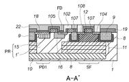
図3は、画素アレイ210を構成する画素ユニットPUの構成例を示すレイアウト図である。図4は、図3におけるA−A’に沿った模式的な断面図である。
FIG. 3 is a layout diagram illustrating a configuration example of the pixel unit PU included in the
この実施形態では、p型領域PRと、p型領域PRの下に形成されたn型の埋め込み層10とによってフォトダイオードPD(PD1、PD2)が形成されている。p型領域PRはアノード、埋め込み層10はカソードである。p型領域PRは、p型の第1領域15と、少なくとも一部が第1領域15とn型の埋め込み層10との間に配置されたp型の第2領域1’とを含む。第1領域15は、主たる電荷蓄積領域として機能する。第2領域1’のp型不純物の濃度は、例えば、p型のシリコン基板(半導体基板)1と同一でありうる。第1領域15のp型不純物の濃度は、第2領域1’のp型不純物の濃度よりも高い。p型領域PRは、n型の表面領域18の下に形成されることが好ましく、この場合には、n型の表面領域18、p型領域PRおよびn型埋め込み層10によって埋め込み型のフォトダイオードPDが構成される。埋め込み型のフォトダイオードは、暗電流によるノイズが小さいことが知られている。
In this embodiment, a photodiode PD (PD1, PD2) is formed by the p-type region PR and the n-type buried
n型の表面領域18の主要不純物の拡散係数は、埋め込み層10の主要不純物の拡散係数より小さいことが好ましい。例えば、n型の表面領域18の主要不純物が砒素(As)であり、埋め込み層10の主要不純物が燐(P)であることが好ましい。砒素(As)は、拡散係数が燐(P)よりも小さいので、表面領域18を砒素(As)で形成することは、その境界の確定が容易であるので微細化に有利である。一方、燐(P)は、砒素(As)に比べて半導体基板の深い位置まで侵入させることが容易であるので、埋め込み層10を燐(P)で形成することは、深い位置に埋め込み層10を形成することを可能にし、感度の向上に有利である。また、燐(P)は、拡散係数が砒素(As)よりも大きいので、燐(P)によって埋め込み層10を形成することは、広く分布したポテンシャル障壁の形成において有利である。また、燐(P)は、イオン半径がシリコン基板1の格子定数より大きいので、シリコン基板1への燐(P)の注入によってシリコン基板1の格子に歪みを生じさせ、不純物金属元素のゲッタリング効果を生じさせるために有利であり、これは点欠陥の改善に寄与する。埋め込み層10は、チャネリング現象を利用して燐(P)を半導体基板1にイオン注入することによって形成されうる。本発明において、注入またはドープする不純物は、砒素(As)および燐(P)に制限されず、他の不純物を使用することもできる。
The diffusion coefficient of the main impurity of the n-
浮遊拡散部FDは、p型の第3領域である。フォトダイオードPDの一部を構成するp型の第1領域15と浮遊拡散部FD(p型の第3領域)との間の領域の上には、転送トランジスタTT(TT1、TT2)のゲート105が配置されている。換言すると、転送トランジスタTTは、p型の第1領域15、浮遊拡散部FD(p型の第3領域)およびゲート105によって構成されている。転送トランジスタTTは、フォトダイオードFDのp型領域(15、1’)に蓄積された正孔を浮遊拡散部FDに転送する。この実施形態では、転送トランジスタTTは、PMOSトランジスタである。転送トランジスタTTのゲート105は、ポリシリコンで構成されうる。
The floating diffusion portion FD is a p-type third region. A
p型の第2領域1’は、断面においてp型の第1領域15を取り囲むように配置されうる。またはp型の第1領域15の素子分離領域側は後述のチャネルストップ領域と接していてもよい。この場合にはp型の第2領域1’は、p型の第1領域15の素子分離領域側を除いてp型の第1領域15を取り囲んでいる。第2領域1’と浮遊拡散部FD(第3領域)とは、n型領域16によって分離されていて、n型領域16に転送トランジスタTTのチャネルが形成される。
The p-type
素子分離領域9は、フォトダイオードPD、転送トランジスタTT、増幅トランジスタSFおよびリセットトランジスタRTが形成されるべき活性領域を分離するように配置されている。活性領域は、図3では、表面領域18、浮遊拡散部FD、拡散領域104、108および110であり、これら以外の領域が素子分離領域9とされうる。素子分離領域9の形成には、典型的には、STI(Shallow Trench Isolation)技術またはLOCOS(Local Oxidation Of Silicon)技術が使用されうる。または拡散分離を使用しても良い。
The
素子分離領域9の少なくとも下側部分(下部側面および下面)を覆う領域には、チャネルストップ領域8が形成される。チャネルストップ領域8の主要不純物の拡散係数は、埋め込み層10の主要不純物の拡散係数より小さいことが好ましい。例えば、チャネルストップ領域8の主要不純物が砒素(As)であり、埋め込み層10の主要不純物が燐(P)であることが好ましい。前述のとおり、砒素(As)は、拡散係数が燐(P)よりも小さいので、チャネルストップ領域8を砒素(As)で形成することは、微細化に有利である。チャネルストップ領域8の主要不純物は、表面領域18の主要不純物と同一でありうる。
A
フォトダイオードPD間には、ポテンシャル障壁11が形成されている。また、必要に応じて、フォトダイオードPDと増幅トランジスタSFおよびリセットトランジスタRTとの間にもポテンシャル障壁11が形成されうる。なお、単一画素の光電変換装置や、画素間の間隔が大きい撮像装置においては、フォトダイオード間のポテンシャル障壁は不要である。また、素子分離領域9が十分に深くまで形成されている場合には、フォトダイオードと増幅トランジスタSFおよびリセットトランジスタRTとの間のポテンシャル障壁は不要である。この実施形態では、ポテンシャル障壁11の形成によってポテンシャル障壁11によって囲まれたp型領域1’が確定される。
A
増幅トランジスタSFのゲート107は、浮遊拡散部FDに対して電気的に接続される。増幅トランジスタSFのゲート107は、ポリシリコンで構成されうる。この実施形態では、増幅トランジスタSFのゲート107は、シェアードコンタクトプラグ102によって浮遊拡散部FDに対して電気的に接続される。シェアードコンタクトプラグ102は、開口率の向上または画素密度の向上に有利である。ここで、シェアードコンタクトプラグは、1つのトランジスタの拡散領域(ソースまたはドレイン)と他のトランジスタのゲートとを1つのコンタクトプラグで電気的に接続するコンタクトプラグである。
The
増幅トランジスタSFは、浮遊拡散部FDに電気的に接続されたゲート107と、拡散領域104、108とを含むPMOSトランジスタである。リセットトランジスタRTは、リセット信号線RESに接続されたゲート106と、浮遊拡散部FDと、拡散領域110とを含むPMOSトランジスタである。リセットトランジスタRTのゲートは、ポリシリコンで構成されうる。
The amplification transistor SF is a PMOS transistor including a
増幅トランジスタSFは、埋め込みチャネル構造を有することが好ましい。これは、増幅トランジスタSFを埋め込みチャネル構造にすることによって1/fノイズを低減することができるからである(1/fノイズは、チャネル幅とチャネル長との積に反比例する)。一方、リセットトランジスタRTおよび転送トランジスタTT(行を選択する選択トランジスタが存在する場合には、当該行選択トランジスタ)、特にリセットトランジスタRTは、表面チャネル構造を有することが好ましい。これは、浮遊拡散部FDへの正孔のリークを抑制するためには、トランジスタのオフ状態が重要であることによる。埋め込みチャネル型のトランジスタでは、ノーマリーオンの状態になりやすく、オフ状態にしにくい場合がある。また、画素の微細化のためには、リセットトランジスタRTおよび転送トランジスタTT(行を選択する選択トランジスタが存在する場合には、当該行選択トランジスタ)を微細化することが有効であり、そのためには、表面チャネル型の方が有利である。 The amplification transistor SF preferably has a buried channel structure. This is because 1 / f noise can be reduced by making the amplification transistor SF have a buried channel structure (1 / f noise is inversely proportional to the product of the channel width and the channel length). On the other hand, the reset transistor RT and the transfer transistor TT (if there is a selection transistor for selecting a row, the row selection transistor), in particular, the reset transistor RT preferably has a surface channel structure. This is because the off state of the transistor is important in order to suppress the leakage of holes to the floating diffusion portion FD. A buried channel transistor tends to be normally on, and may be difficult to turn off. Further, in order to miniaturize the pixels, it is effective to miniaturize the reset transistor RT and the transfer transistor TT (if there is a selection transistor for selecting a row, the row selection transistor). The surface channel type is more advantageous.
この実施形態では、PMOSトランジスタで構成される増幅トランジスタSFを埋め込みチャネル構造とするために、増幅トランジスタSFのゲートがn型導電パターンで構成される。PMOSトランジスタで構成される転送トランジスタTTおよびリセットトランジスタRTのゲート107は、p型導電パターンで構成されてもよいが、n型導電パターンで構成されてもよい。いずれの場合であっても、転送トランジスタTTおよびリセットトランジスタRTを表面チャネル構造とすることができる。転送トランジスタTTおよびリセットトランジスタRTのゲートがn型導電パターンで構成される場合には、チャネル幅を小さくすることにより(例えば1μmよりも小さくすることにより)、容易に表面チャネル構造を得ることができる。増幅トランジスタSFをより安定して埋め込みチャネル構造とするために、ゲート絶縁膜とシリコン基板1との界面から所定深さの位置にチャネルドープを行ってもよい。チャネルドープする不純物の導電型は、ソース・ドレイン領域と同じ導電型であり、濃度はソース・ドレイン領域よりも低くされる。
In this embodiment, in order to make the amplification transistor SF formed of a PMOS transistor have a buried channel structure, the gate of the amplification transistor SF is formed of an n-type conductive pattern. The
上記のとおり、この実施形態では、PMOSトランジスタで構成される増幅トランジスタSFのゲート107がn型の導電パターンである。一方、シェアードコンタクトプラグ102によってゲート107と接続される浮遊拡散部FDは、この実施形態では、p型の拡散領域である。したがって、シェアードコンタクトプラグ102は、ゲート107としてのn型の導電パターンと、浮遊拡散部FDとしてのp型の拡散領域との双方に電気的に接続されなければならない。更に、この電気的な接続は、集積度が高く低ノイズで高速な撮像装置(半導体装置)を提供するためには、オーミック接触でなされるべきである。そのための方法については、以下の半導体装置の製造方法に関する説明の中で図5および図6を参照しながら説明される。
As described above, in this embodiment, the
以下、図5〜図11を参照しながら本発明の半導体装置の製造方法の好適な実施形態として撮像装置200の製造方法を例示的に説明する。なお、以下では、第1導電型をp型、第2導電型をn型と考えてそのような注釈を加えながら説明するが、この逆に考えてもよい。
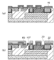
Hereinafter, a method for manufacturing the
まず、図7(a)に示す工程では、p型のシリコン基板1を準備する。そして、シリコン基板1の表面に10〜200Åのシリコン酸化膜を形成した後に400〜600Åのポリシリコン膜、150〜200Åのシリコン窒化膜を順に形成し、それらをパタニングしてマスクを形成する。
First, in the step shown in FIG. 7A, a p-
次いで、図7(b)に示す工程では、図7(a)に示す工程で形成したマスクの開口部をエッチングして素子分離領域9の形成のためのトレンチ6を形成する。次いで、図7(c)に示す工程では、トレンチ6の下および下部側方に砒素(As)を150〜200KeVで注入してチャネルストップ領域8を形成する。次いで、図7(d)に示す工程では、トレンチ6中に素子分離領域(STI)9を形成する。
Next, in the step shown in FIG. 7B, the opening of the mask formed in the step shown in FIG. 7A is etched to form a trench 6 for forming the
次いで、図8(a)に示す工程では、p型(第1導電型)のシリコン基板1の深部に燐(P)を4000〜8000KeVで注入してn型(第2導電型)の埋め込み層1を形成する。ここでは、チャネリング現象を利用して可能な限り深部に燐(P)を注入することが好ましい。次いで、図8(b)に示す工程では、フォトダイオードPD間、および、必要に応じて、フォトダイオードPDと増幅トランジスタSFおよびリセットトランジスタRTとの間にポテンシャル障壁11を形成する。ポテンシャル障壁11は、シリコン基板1に対して、例えば、燐(P)を2000〜2500KeVで注入し、次いで、燐(P)を1000〜1500KeVで注入し、次いで、砒素(As)を700〜750KeVで注入することによって形成されうる。
8A, phosphorus (P) is implanted into the deep portion of the p-type (first conductivity type)
次いで、図8(c)に示す工程では、増幅トランジスタSFおよびリセットトランジスタRTを形成すべき領域にイオンを注入して目標とするポテンシャル構造を形成する。例えば、このイオン注入工程にはチャネルドープなどの工程が含まれる。ここで、前述のとおり、増幅トランジスタSFが埋め込みチャネル構造となり、リセットトランジスタRTが表面チャネル構造となるようにポテンシャル構造が形成されることが好ましい。 Next, in a step shown in FIG. 8C, ions are implanted into a region where the amplification transistor SF and the reset transistor RT are to be formed to form a target potential structure. For example, this ion implantation process includes a process such as channel doping. Here, as described above, the potential structure is preferably formed so that the amplification transistor SF has a buried channel structure and the reset transistor RT has a surface channel structure.
次いで、図9(a)に示す工程では、ゲート酸化膜およびポリシリコン電極を形成した後にこれらをパタニングしてゲート105、107(および106(不図示))を形成する。ゲート105、107(および106(不図示))のうち少なくとも増幅トランジスタSF(ここでは、PMOSトランジスタ)のゲート107は、n型不純物(第2導電型)が注入またはドープされてn型導電パターン(第2導電型領域)とされる。なお、画素アレイ210以外の回路である周辺回路(行選択回路240、読出回路220、列選択回路230)のPMOSトランジスタのゲートは、p型導電パターンで構成されることが好ましい。
Next, in the step shown in FIG. 9A, after forming a gate oxide film and a polysilicon electrode, they are patterned to form
次いで、図9(b)に示す工程では、フォトダイオードPDの領域に硼素(B)を50〜150KeVで注入し、p型領域PRの一部を構成する第1領域15を形成する。次いで、図9(c)に示す工程では、転送トランジスタTTの下部から浮遊拡散部FD側に延びる領域に燐(P)を50〜150KeVで注入し、n型領域16を形成する。
Next, in the step shown in FIG. 9B, boron (B) is implanted into the region of the photodiode PD at 50 to 150 KeV to form the
次いで、図10(a)に示す工程では、PMOSトランジスタの拡散領域とするべき領域にp型(第1導電型)の半導体領域を形成するための不純物である硼素(B)を10〜15KeVで注入する。これにより、浮遊拡散部(第1導電型領域)FD、拡散領域108、104(および110(不図示))が形成される。またその他のトランジスタのソース・ドレイン領域も形成する。次いで、図10(b)に示す工程では、表面領域18を形成するべき領域にn型(第2導電型)の半導体領域を形成するための不純物である砒素(As)を50〜100KeVで注入して表面領域18を形成する。
Next, in the process shown in FIG. 10A, boron (B), which is an impurity for forming a p-type (first conductivity type) semiconductor region in a region to be a diffusion region of the PMOS transistor, is 10 to 15 KeV. inject. Thereby, the floating diffusion part (first conductivity type region) FD and the
次いで、図11(a)に示す工程では、50〜100Åのシリコン酸化膜、400〜600Åの反射防止シリコン窒化膜および500〜1000Åの保護シリコン酸化膜を含む膜19を形成する。次いで、図11(b)に示す工程(ホール形成工程)では、層間絶縁膜(例えば、500〜1500ÅのNSG、10000〜15000ÅのBPSG)22を形成し、更に、層間絶縁膜22にコンタクトホール23を形成する。
Next, in the step shown in FIG. 11A, a
図5は、図3におけるB−B’に沿った模式的な断面図である。図5において、コンタクトホール23は、図11(b)に示す工程で形成されるコンタクトホールであり、n型(第1導電型)の浮遊拡散部(第1導電型領域)FDとp型(第2導電型)のゲート(第2導電型領域)107とに対して共通のコンタクトホールである。図5は、図11(b)に示すホール形成工程の後に実施される注入工程を模式的に示している。注入工程では、浮遊拡散部(第1導電型領域)FDとゲート(第2導電型領域)107の少なくとも一方に対して不純物が注入される。ここで、不純物の注入は、浮遊拡散部(第1導電型領域)FDと後の工程で形成されるシェアードコンタクトプラグ102とがオーミック接触し、かつゲート(第2導電型領域)107とシェアードコンタクトプラグ102とがオーミック接触するようになされる。
FIG. 5 is a schematic cross-sectional view along B-B ′ in FIG. 3. In FIG. 5, a
例えば、浮遊拡散部FDにおけるp型の不純物の濃度が1×1017〜1×1021(/cm3)であり、増幅トランジスタSFのゲート107のn型(第2導電型)のn型の不純物の濃度が7×1019〜7×1021(/cm3)である場合を考える。この場合は、p型の半導体領域を形成するための不純物(硼素)をドーズ量1×1013〜1×1015(/cm2)で浮遊拡散部(第1導電型領域)FDおよびゲート(第2導電型領域)107の双方に同時に注入すればよい。これにより、浮遊拡散部(第1導電型領域)FDには、シェアードコンタクトプラグ102とのオーミック接触の条件(例えば、不純物濃度5×1019〜1×1021(/cm3))を満たす接触領域501が形成される。また、ゲート(第2導電型領域)107には、シェアードコンタクトプラグ102とのオーミック接触の条件(例えば、不純物濃度5×1019〜1×1021(/cm3))を満たす接触領域502が形成される。以上は、第1導電型領域における主要不純物の濃度が第2導電型領域における主要不純物の濃度よりも低い場合に、第1導電型の半導体領域を形成するための不純物を第1導電型領域および第2導電型領域に対して同時に注入する例である。これとは逆に、第2導電型領域における主要不純物の濃度が第1導電型領域における主要不純物の濃度よりも低い場合に、第2導電型の半導体領域を形成するための不純物を第1導電型領域および第2導電型領域に対して同時に注入してもよい。
For example, the concentration of the p-type impurity in the floating diffusion portion FD is 1 × 10 17 to 1 × 10 21 (/ cm 3 ), and the n-type (second conductivity type) of the
図6は、図11(b)に示すホール形成工程の後に実施される注入工程の他の例を模式的に示している。この例では、注入工程を第1工程および第2工程を含む。第1工程では、符号503で示すように、ゲート(第2導電型領域)107よりも浮遊拡散部(第1導電型領域)FDに対してより多くの不純物が注入されるように、浮遊拡散部FDおよびゲート107を含む部材(基板)の表面に対して斜め方向に不純物を注入する。第2工程では、符号504で示すように、浮遊拡散部(第1導電型領域)FDよりもゲート(第2導電型領域)107に対してより多くの不純物が注入されるように、浮遊拡散部FDおよびゲート107を含む部材(基板)の表面に対して斜め方向に不純物を注入する。この例によれば、浮遊拡散部(第1導電型領域)FDに対する不純物の注入量とゲート(第2導電型領域)107に対する不純物の注入量とを個別に制御することができる。
FIG. 6 schematically shows another example of the injection step performed after the hole forming step shown in FIG. In this example, the injection process includes a first process and a second process. In the first step, as indicated by
以上の説明において、浮遊拡散部FDおよびゲート107は、第1または第2導電型領域の一例であり、第1導電型領域および第2導電型領域の一方がトランジスタのソースまたはドレインで他方がゲートであってもよい。
In the above description, the floating diffusion FD and the
次いで、図4に示すプラグ形成工程では、まず、シェアードコンタクトホールを含むコンタクトホール23にバリアメタル(Ti/TiN)を形成する。次いで、導電材料(タングステン(W))を充填することによってシェアードコンタクトプラグ102(および105a、111〜113(不図示))を形成する。
Next, in the plug formation step shown in FIG. 4, first, a barrier metal (Ti / TiN) is formed in the
次に、本発明の第2タイプの撮像装置への適用について簡単に説明する。図12は、画素アレイ210の画素ユニットPUの他の構成例を示す回路図である。この構成例では、図2に示す構成例におけるPMOSトランジスタがNMOSトランジスタで置き換えられ、フォトダイオードPDの接続が逆になっている。このような第2タイプの撮像装置の製造においては、上記の説明におけるn型をp型に変更し、p型をn型に変更して考えればよい。この場合、増幅トランジスタSFのゲートは、p型導電パターンとなり、それがシェアードコンタクトプラグ102によって接続される浮遊拡散部FDは、n型の領域となる。
Next, application of the present invention to the second type imaging apparatus will be briefly described. FIG. 12 is a circuit diagram illustrating another configuration example of the pixel unit PU of the
図13は、本発明の好適な実施形態のカメラの概略構成を示す図である。なお、カメラの概念には、撮影を主目的とする装置のみならず、撮影機能を補助的に備える装置(例えば、パーソナルコンピュータ、携帯端末)も含まれる。カメラ400は、上記の撮像装置200に代表される固体撮像装置1004を備える。被写体の光学像は、レンズ1002によって固体撮像装置1004の撮像面に結像する。レンズ1002の外側には、レンズ1002のプロテクト機能とメインスイッチを兼ねるバリア1001が設けられうる。レンズ1002には、それから出射される光の光量を調節するための絞り1003が設けられうる。固体撮像装置1004から出力される撮像信号は、撮像信号処理回路1005によって各種の補正、クランプ等の処理が施される。撮像信号処理回路1005から出力される撮像信号は、A/D変換器1006でアナログ−ディジタル変換される。A/D変換器1006から出力される画像データは、信号処理部1007によって補正、データ圧縮などの信号処理がなされる。固体撮像装置1004、撮像信号処理回路1005、A/D変換器1006及び信号処理部1007は、タイミング発生部1008が発生するタイミング信号にしたがって動作する。
FIG. 13 is a diagram showing a schematic configuration of a camera according to a preferred embodiment of the present invention. Note that the concept of a camera includes not only a device mainly for photographing, but also a device (for example, a personal computer or a portable terminal) that is supplementarily provided with a photographing function. The
ブロック1005〜1008は、固体撮像装置1004と同一チップ上に形成されてもよい。カメラ400の各ブロックは、全体制御・演算部1009によって制御される。カメラ400は、その他、画像データを一時的に記憶するためのメモリ部1010、記録媒体への画像の記録又は読み出しのための記録媒体制御インターフェース部1011を備える。記録媒体1012は、半導体メモリ等を含んで構成され、着脱が可能である。カメラ400は、外部コンピュータ等と通信するための外部インターフェース(I/F)部1013を備えてもよい。
The
次に、図13に示すカメラ400の動作について説明する。バリア1001のオープンに応じて、メイン電源、コントロール系の電源、A/D変換器1006等の撮像系回路の電源が順にオンする。その後、露光量を制御するために、全体制御・演算部1009が絞り1003を開放にする。固体撮像装置1004から出力された信号は、撮像信号処理回路1005をスルーしてA/D変換器1006へ提供される。A/D変換器1006は、その信号をA/D変換して信号処理部1007に出力する。信号処理部1007は、そのデータを処理して全体制御・演算部1009に提供し、全体制御・演算部1009において露出量を決定する演算を行う。全体制御・演算部1009は、決定した露出量に基づいて絞りを制御する。
Next, the operation of the
次に、全体制御・演算部1009は、固体撮像装置1004から出力され信号処理部1007で処理された信号にから高周波成分を取り出して、高周波成分に基づいて被写体までの距離を演算する。その後、レンズ1002を駆動して、合焦か否かを判断する。合焦していないと判断したときは、再びレンズ1002を駆動し、距離を演算する。
Next, the overall control /
そして、合焦が確認された後に本露光が始まる。露光が終了すると、固体撮像装置1004から出力された撮像信号は、撮像信号処理回路1005において補正等がされ、A/D変換器1006でA/D変換され、信号処理部1007で処理される。信号処理部1007で処理された画像データは、全体制御・演算部1009によりメモリ部1010に蓄積される。
Then, after the in-focus state is confirmed, the main exposure starts. When the exposure is completed, the imaging signal output from the solid-
その後、メモリ部1010に蓄積された画像データは、全体制御・演算部1009の制御により記録媒体制御I/F部を介して記録媒体1012に記録される。また、画像データは、外部I/F部1013を通してコンピュータ等に提供されて処理されうる。
Thereafter, the image data stored in the
FD 浮遊拡散部
23 コンタクトホール
107 ゲート
501、502 接触領域
8 チャネルストップ層
9 素子分離領域
FD floating
Claims (8)
前記第1導電型領域および前記第2導電型領域の少なくとも一方に対して不純物を注入する注入工程と、
前記コンタクトホールに導電材料を充填してシェアードコンタクトプラグを形成するプラグ形成工程とを含み、
前記注入工程では、前記第1導電型領域と前記シェアードコンタクトプラグとがオーミック接触し、かつ前記第2導電型領域と前記シェアードコンタクトプラグとがオーミック接触するように、前記第1導電型領域および前記第2導電型領域の少なくとも一方に対して不純物を注入し、
前記第1導電型領域における主要不純物の濃度が前記第2導電型領域における主要不純物の濃度よりも低く、
前記注入工程では、前記第1導電型の半導体領域を形成するための不純物を前記第1導電型領域および前記第2導電型領域に対して同時に注入する、
ことを特徴とする半導体装置の製造方法。 The first conductivity type region which is a first conductivity type region and the second conductivity type region which is a second conductivity type region different from the first conductivity type are exposed. Forming a common contact hole for one conductivity type region and the second conductivity type region;
An implantation step of implanting impurities into at least one of the first conductivity type region and the second conductivity type region;
Forming a shared contact plug by filling the contact hole with a conductive material,
In the implantation step, the first conductivity type region and the shared contact plug are in ohmic contact with each other, and the second conductivity type region and the shared contact plug are in ohmic contact with each other. Impurities are implanted into at least one of the second conductivity type regions ,
A concentration of main impurities in the first conductivity type region is lower than a concentration of main impurities in the second conductivity type region;
In the implantation step, an impurity for forming the first conductivity type semiconductor region is simultaneously implanted into the first conductivity type region and the second conductivity type region.
A method for manufacturing a semiconductor device.
前記第1導電型領域および前記第2導電型領域の少なくとも一方に対して不純物を注入する注入工程と、An implantation step of implanting impurities into at least one of the first conductivity type region and the second conductivity type region;
前記コンタクトホールに導電材料を充填してシェアードコンタクトプラグを形成するプラグ形成工程とを含み、Forming a shared contact plug by filling the contact hole with a conductive material,
前記注入工程では、前記第1導電型領域と前記シェアードコンタクトプラグとがオーミック接触し、かつ前記第2導電型領域と前記シェアードコンタクトプラグとがオーミック接触するように、前記第1導電型領域および前記第2導電型領域の少なくとも一方に対して不純物を注入し、In the implantation step, the first conductivity type region and the shared contact plug are in ohmic contact with each other, and the second conductivity type region and the shared contact plug are in ohmic contact with each other. Impurities are implanted into at least one of the second conductivity type regions,
前記第2導電型領域における主要不純物の濃度が前記第1導電型領域における主要不純物の濃度よりも低く、A concentration of main impurities in the second conductivity type region is lower than a concentration of main impurities in the first conductivity type region;
前記注入工程では、前記第2導電型の半導体領域を形成するための不純物を前記第1導電型領域および前記第2導電型領域に対して同時に注入する、In the implantation step, an impurity for forming the second conductivity type semiconductor region is simultaneously implanted into the first conductivity type region and the second conductivity type region.
ことを特徴とする半導体装置の製造方法。A method for manufacturing a semiconductor device.
前記第1導電型領域および前記第2導電型領域の少なくとも一方に対して不純物を注入する注入工程と、An implantation step of implanting impurities into at least one of the first conductivity type region and the second conductivity type region;
前記コンタクトホールに導電材料を充填してシェアードコンタクトプラグを形成するプラグ形成工程とを含み、Forming a shared contact plug by filling the contact hole with a conductive material,
前記注入工程では、前記第1導電型領域と前記シェアードコンタクトプラグとがオーミック接触し、かつ前記第2導電型領域と前記シェアードコンタクトプラグとがオーミック接触するように、前記第1導電型領域および前記第2導電型領域の少なくとも一方に対して不純物を注入し、In the implantation step, the first conductivity type region and the shared contact plug are in ohmic contact with each other, and the second conductivity type region and the shared contact plug are in ohmic contact with each other. Impurities are implanted into at least one of the second conductivity type regions,
前記注入工程は、The injection step includes
前記第2導電型領域よりも前記第1導電型領域に対してより多くの不純物が注入されるように、前記第1導電型領域および前記第2導電型領域を含む部材の表面に対して斜め方向に不純物を注入する工程と、The surface of the member including the first conductivity type region and the second conductivity type region is inclined so that more impurities are implanted into the first conductivity type region than the second conductivity type region. Implanting impurities in the direction;
前記第1導電型領域よりも前記第2導電型領域に対してより多くの不純物が注入されるように、前記部材の表面に対して斜め方向に不純物を注入する工程と、を含む、Injecting impurities in an oblique direction with respect to the surface of the member such that more impurities are implanted into the second conductivity type region than the first conductivity type region.
ことを特徴とする半導体装置の製造方法。A method for manufacturing a semiconductor device.
ことを特徴とする請求項1乃至3のいずれか1項に記載の半導体装置の製造方法。 A step of forming a barrier metal in the contact hole after the hole forming step and before the plug forming step;
The method of manufacturing a semiconductor device according to any one of claims 1 to 3, characterized in that.
ことを特徴とする請求項1乃至4のいずれか1項に記載の半導体装置の製造方法。 The first conductivity type region is a source or drain, and the second conductivity type region is a gate;
The method of manufacturing a semiconductor device according to any one of claims 1 to 4, characterized in that.
前記第1導電型領域は前記浮遊拡散部であり、前記第2導電型領域は前記増幅トランジスタのゲートである、
ことを特徴とする請求項1乃至4のいずれか1項に記載の半導体装置の製造方法。 The semiconductor device includes a photoelectric conversion device, and the photoelectric conversion device includes a photodiode, a floating diffusion portion, a transfer transistor that transfers charges accumulated in a storage region of the photodiode to the floating diffusion portion, and Including an amplification transistor for amplifying a signal appearing in the floating diffusion portion,
The first conductivity type region is the floating diffusion portion, and the second conductivity type region is a gate of the amplification transistor.
The method of manufacturing a semiconductor device according to any one of claims 1 to 4, characterized in that.
ことを特徴とする請求項6に記載の半導体装置の製造方法。 The amplification transistor has a buried channel structure.
The method of manufacturing a semiconductor device according to claim 6 .
前記シェアードコンタクトプラグは、前記第1接触領域および前記第2接触領域に直接接触する、
ことを特徴とする請求項1乃至7のいずれか1項に記載の半導体装置の製造方法。 The implantation step forms a first contact region in a part of the first conductivity type region and a second contact region in a part of the second conductivity type region,
The shared contact plug is in direct contact with the first contact region and the second contact region;
The method of manufacturing a semiconductor device according to any one of claims 1 to 7, characterized in that.
Priority Applications (2)
| Application Number | Priority Date | Filing Date | Title |
|---|---|---|---|
| JP2009026702A JP5451098B2 (en) | 2009-02-06 | 2009-02-06 | Manufacturing method of semiconductor device |
| US12/692,804 US8053272B2 (en) | 2009-02-06 | 2010-01-25 | Semiconductor device fabrication method |
Applications Claiming Priority (1)
| Application Number | Priority Date | Filing Date | Title |
|---|---|---|---|
| JP2009026702A JP5451098B2 (en) | 2009-02-06 | 2009-02-06 | Manufacturing method of semiconductor device |
Publications (3)
| Publication Number | Publication Date |
|---|---|
| JP2010182976A JP2010182976A (en) | 2010-08-19 |
| JP2010182976A5 JP2010182976A5 (en) | 2012-03-01 |
| JP5451098B2 true JP5451098B2 (en) | 2014-03-26 |
Family
ID=42540752
Family Applications (1)
| Application Number | Title | Priority Date | Filing Date |
|---|---|---|---|
| JP2009026702A Expired - Fee Related JP5451098B2 (en) | 2009-02-06 | 2009-02-06 | Manufacturing method of semiconductor device |
Country Status (2)
| Country | Link |
|---|---|
| US (1) | US8053272B2 (en) |
| JP (1) | JP5451098B2 (en) |
Families Citing this family (17)
| Publication number | Priority date | Publication date | Assignee | Title |
|---|---|---|---|---|
| JP2010206181A (en) * | 2009-02-06 | 2010-09-16 | Canon Inc | Photoelectric conversion apparatus and imaging system |
| JP2010206178A (en) | 2009-02-06 | 2010-09-16 | Canon Inc | Photoelectric conversion apparatus, and method of manufacturing photoelectric conversion apparatus |
| JP2010206174A (en) | 2009-02-06 | 2010-09-16 | Canon Inc | Photoelectric converter, method of manufacturing the same, and camera |
| JP2010206172A (en) | 2009-02-06 | 2010-09-16 | Canon Inc | Image sensing device, and camera |
| JP2010206173A (en) | 2009-02-06 | 2010-09-16 | Canon Inc | Photoelectric conversion device and camera |
| JP5489855B2 (en) | 2010-05-14 | 2014-05-14 | キヤノン株式会社 | Method for manufacturing solid-state imaging device |
| KR101770289B1 (en) * | 2010-09-29 | 2017-08-23 | 삼성전자주식회사 | Image sensor and method of forming the same |
| JP6084922B2 (en) | 2011-06-23 | 2017-02-22 | パナソニック株式会社 | Solid-state imaging device |
| JP5930650B2 (en) * | 2011-10-07 | 2016-06-08 | キヤノン株式会社 | Manufacturing method of semiconductor device |
| JP2013247347A (en) | 2012-05-29 | 2013-12-09 | Canon Inc | Semiconductor device and manufacturing method of the same |
| KR102025339B1 (en) | 2013-03-07 | 2019-09-26 | 삼성전자 주식회사 | Semiconductor device having a conductive plug |
| JP6161454B2 (en) * | 2013-07-25 | 2017-07-12 | キヤノン株式会社 | Photoelectric conversion device, manufacturing method thereof, and camera |
| JP6491509B2 (en) * | 2015-03-25 | 2019-03-27 | キヤノン株式会社 | Solid-state imaging device and manufacturing method thereof |
| EP3113224B1 (en) | 2015-06-12 | 2020-07-08 | Canon Kabushiki Kaisha | Imaging apparatus, method of manufacturing the same, and camera |
| JP6861471B2 (en) * | 2015-06-12 | 2021-04-21 | キヤノン株式会社 | Imaging device and its manufacturing method and camera |
| JP7084735B2 (en) * | 2018-01-31 | 2022-06-15 | キヤノン株式会社 | Manufacturing method of semiconductor device |
| JP7327916B2 (en) * | 2018-09-11 | 2023-08-16 | キヤノン株式会社 | Photoelectric conversion device and equipment |
Family Cites Families (29)
| Publication number | Priority date | Publication date | Assignee | Title |
|---|---|---|---|---|
| JPH03120828A (en) * | 1989-10-04 | 1991-05-23 | Nec Corp | Semiconductor device and manufacture thereof |
| EP0510604A3 (en) | 1991-04-23 | 2001-05-09 | Canon Kabushiki Kaisha | Semiconductor device and method of manufacturing the same |
| JPH08130246A (en) * | 1994-10-28 | 1996-05-21 | Ricoh Co Ltd | Semiconductor device and fabrication thereof |
| JP3292657B2 (en) | 1995-04-10 | 2002-06-17 | キヤノン株式会社 | Thin film transistor and method for manufacturing liquid crystal display device using the same |
| JP3248470B2 (en) * | 1997-11-21 | 2002-01-21 | 日本電気株式会社 | Charge transfer device and method of manufacturing charge transfer device |
| JP2000349096A (en) * | 1999-06-01 | 2000-12-15 | Matsushita Electric Ind Co Ltd | Compound field effect transistor and its manufacture |
| KR100304503B1 (en) * | 1999-07-09 | 2001-11-01 | 김영환 | Method for fabricating a semiconductor device |
| US20070106371A1 (en) * | 2002-01-29 | 2007-05-10 | Arindam Datta | Biodegradable stent |
| JP4155568B2 (en) | 2003-08-07 | 2008-09-24 | キヤノン株式会社 | Solid-state imaging device and camera |
| JP4439888B2 (en) | 2003-11-27 | 2010-03-24 | イノテック株式会社 | MOS type solid-state imaging device and driving method thereof |
| US7323731B2 (en) | 2003-12-12 | 2008-01-29 | Canon Kabushiki Kaisha | Photoelectric conversion device, method of manufacturing photoelectric conversion device, and image pickup system |
| KR100618820B1 (en) * | 2004-02-10 | 2006-09-12 | 삼성전자주식회사 | Photodiode having light-absorption part which is seperated by PN junction and method of fabrication the same |
| JP5224633B2 (en) | 2004-03-30 | 2013-07-03 | キヤノン株式会社 | Manufacturing method of semiconductor device |
| WO2005109512A1 (en) | 2004-05-06 | 2005-11-17 | Canon Kabushiki Kaisha | Photoelectric conversion device and manufacturing method thereof |
| US7540198B2 (en) | 2004-06-15 | 2009-06-02 | Canon Kabushiki Kaisha | Semiconductor device |
| KR100577312B1 (en) * | 2004-07-05 | 2006-05-10 | 동부일렉트로닉스 주식회사 | Phototransistor of CMOS image sensor and method for fabricating the same |
| JP4513497B2 (en) | 2004-10-19 | 2010-07-28 | ソニー株式会社 | Solid-state imaging device |
| US8120077B2 (en) | 2004-12-16 | 2012-02-21 | Panasonic Corporation | Solid-state imaging device comprising doped channel stop at isolation regions to suppress noise |
| KR100670803B1 (en) | 2004-12-21 | 2007-01-19 | 한국전자통신연구원 | Device using ambipolar transport in SB-MOSFET |
| CN100536151C (en) | 2005-03-11 | 2009-09-02 | 富士通微电子株式会社 | Imaging sensor with built-in photodiode area and preparation method thereof |
| KR100690884B1 (en) | 2005-04-28 | 2007-03-09 | 삼성전자주식회사 | Image sensor and fabricating method for the same |
| US20070023796A1 (en) | 2005-07-27 | 2007-02-01 | International Business Machines Corporation | Pinning layer for pixel sensor cell and method thereof |
| JP2007073544A (en) | 2005-09-02 | 2007-03-22 | Matsushita Electric Ind Co Ltd | Solid state imaging device and its manufacturing method |
| US7728277B2 (en) | 2005-11-16 | 2010-06-01 | Eastman Kodak Company | PMOS pixel structure with low cross talk for active pixel image sensors |
| KR100761829B1 (en) | 2005-12-15 | 2007-09-28 | 삼성전자주식회사 | semiconductor device, CMOS image sensor, method for manufacturing the semiconductor device and method for manufacturing the CMOS image sensor |
| KR100837271B1 (en) | 2006-08-10 | 2008-06-12 | 삼성전자주식회사 | Semiconductor device and method for forming the same |
| JP5305622B2 (en) * | 2006-08-31 | 2013-10-02 | キヤノン株式会社 | Method for manufacturing photoelectric conversion device |
| JP2008153566A (en) | 2006-12-20 | 2008-07-03 | Matsushita Electric Ind Co Ltd | Solid-state imaging apparatus, and method of manufacturing the same |
| JP2010206172A (en) * | 2009-02-06 | 2010-09-16 | Canon Inc | Image sensing device, and camera |
-
2009
- 2009-02-06 JP JP2009026702A patent/JP5451098B2/en not_active Expired - Fee Related
-
2010
- 2010-01-25 US US12/692,804 patent/US8053272B2/en not_active Expired - Fee Related
Also Published As
| Publication number | Publication date |
|---|---|
| US8053272B2 (en) | 2011-11-08 |
| US20100203670A1 (en) | 2010-08-12 |
| JP2010182976A (en) | 2010-08-19 |
Similar Documents
| Publication | Publication Date | Title |
|---|---|---|
| JP5451098B2 (en) | Manufacturing method of semiconductor device | |
| US8953076B2 (en) | Photoelectric conversion device and camera having a photodiode cathode formed by an n-type buried layer | |
| KR100537546B1 (en) | Solid-state image sensing device and camera system using the same | |
| KR101272423B1 (en) | Image sensing device and camera | |
| US8723285B2 (en) | Photoelectric conversion device manufacturing method thereof, and camera | |
| JP5723094B2 (en) | Solid-state imaging device and camera | |
| JP2014045219A (en) | Solid state image pickup device | |
| US11417691B2 (en) | Image sensor including dummy patterns positioned between adjacent transfer gates | |
| JP2011114302A (en) | Method of manufacturing semiconductor device, semiconductor device, solid-state imaging device, and solid-state imaging apparatus | |
| JP2013045879A (en) | Semiconductor device, semiconductor device manufacturing method, solid state image pickup device, solid state image pickup device manufacturing method and electronic apparatus | |
| JP2012109540A (en) | Method for manufacturing solid state imaging device | |
| JP2005268814A (en) | Solid state imaging device and camera system using the same | |
| JP4435063B2 (en) | Solid-state imaging device and camera system using the solid-state imaging device | |
| JP5478871B2 (en) | Photoelectric conversion device, imaging system, and method of manufacturing photoelectric conversion device | |
| JP2007184368A (en) | Solid-state image sensor | |
| JP4863517B2 (en) | Photoelectric conversion device and camera | |
| JP2015084425A (en) | Photoelectric conversion device, method of manufacturing the same, and camera |
Legal Events
| Date | Code | Title | Description |
|---|---|---|---|
| A521 | Request for written amendment filed |
Free format text: JAPANESE INTERMEDIATE CODE: A523 Effective date: 20120118 |
|
| A621 | Written request for application examination |
Free format text: JAPANESE INTERMEDIATE CODE: A621 Effective date: 20120118 |
|
| A977 | Report on retrieval |
Free format text: JAPANESE INTERMEDIATE CODE: A971007 Effective date: 20130906 |
|
| A131 | Notification of reasons for refusal |
Free format text: JAPANESE INTERMEDIATE CODE: A131 Effective date: 20130913 |
|
| A521 | Request for written amendment filed |
Free format text: JAPANESE INTERMEDIATE CODE: A523 Effective date: 20131108 |
|
| TRDD | Decision of grant or rejection written | ||
| A01 | Written decision to grant a patent or to grant a registration (utility model) |
Free format text: JAPANESE INTERMEDIATE CODE: A01 Effective date: 20131129 |
|
| A61 | First payment of annual fees (during grant procedure) |
Free format text: JAPANESE INTERMEDIATE CODE: A61 Effective date: 20131226 |
|
| R151 | Written notification of patent or utility model registration |
Ref document number: 5451098 Country of ref document: JP Free format text: JAPANESE INTERMEDIATE CODE: R151 |
|
| LAPS | Cancellation because of no payment of annual fees |