JP5449032B2 - Memory system - Google Patents
Memory system Download PDFInfo
- Publication number
- JP5449032B2 JP5449032B2 JP2010121728A JP2010121728A JP5449032B2 JP 5449032 B2 JP5449032 B2 JP 5449032B2 JP 2010121728 A JP2010121728 A JP 2010121728A JP 2010121728 A JP2010121728 A JP 2010121728A JP 5449032 B2 JP5449032 B2 JP 5449032B2
- Authority
- JP
- Japan
- Prior art keywords
- data
- memory
- output
- nth
- clock
- Prior art date
- Legal status (The legal status is an assumption and is not a legal conclusion. Google has not performed a legal analysis and makes no representation as to the accuracy of the status listed.)
- Expired - Fee Related
Links
Images


Classifications
-
- G—PHYSICS
- G06—COMPUTING; CALCULATING OR COUNTING
- G06F—ELECTRIC DIGITAL DATA PROCESSING
- G06F1/00—Details not covered by groups G06F3/00 - G06F13/00 and G06F21/00
- G06F1/04—Generating or distributing clock signals or signals derived directly therefrom
- G06F1/10—Distribution of clock signals, e.g. skew
Landscapes
- Engineering & Computer Science (AREA)
- Theoretical Computer Science (AREA)
- Physics & Mathematics (AREA)
- General Engineering & Computer Science (AREA)
- General Physics & Mathematics (AREA)
- Memory System (AREA)
- Dram (AREA)
Description
本発明は、メモリコントローラからメモリに対してクロックを入力するとともに、前記クロックに同期してメモリからメモリコントローラにデータが出力されるメモリシステムに関する。 The present invention relates to a memory system in which a clock is input from a memory controller to a memory and data is output from the memory to the memory controller in synchronization with the clock.
メモリとメモリコントローラからなるメモリシステムにおいては、メモリとメモリコントローラ間でのデータ転送の高速化が求められている。特許文献1〜3には、高速化が可能なメモリシステムとして、例えば、EDO(Extended Data Out)タイプのDRAMやSDRAM(Syncronous DRAM)の様な、半導体メモリ外部から入力されるクロックに同期して連続したデータを出力可能なメモリシステムが開示されている。このようなメモリシステムではクロックに同期してインクリメントしたアドレスのデータが出力される。
In a memory system including a memory and a memory controller, it is required to increase the speed of data transfer between the memory and the memory controller. In
図9のタイミングチャートを参照して、クロックに同期してインクリメントしたアドレスのデータを出力する一例を説明する。クロックはメモリコントローラからメモリに印加される制御信号である。データはクロックに同期してメモリからメモリコントローラに出力される。データを読み出す前にはメモリコントローラからメモリに対して、アドレスを指定してデータの読み出しを指示するコマンドが発行される。 An example of outputting address data incremented in synchronization with a clock will be described with reference to the timing chart of FIG. The clock is a control signal applied from the memory controller to the memory. Data is output from the memory to the memory controller in synchronization with the clock. Before reading data, the memory controller issues a command for designating an address to the memory by designating an address.
時間t901でメモリコントローラからクロックが出力されると、メモリはクロックの立下りを基準にして一定時間後の時間t903までにデータ線にデータ(データ1)の出力を開始する。この期間をRead Access Time(tREA)という。 When a clock is output from the memory controller at time t901, the memory starts outputting data (data 1) to the data line by time t903 after a predetermined time with reference to the falling edge of the clock. This period is referred to as Read Access Time (tREA).
時間t904でメモリコントローラからクロックが出力されると、メモリはクロックの立下りを基準にして一定時間後の時間t905以降に前のデータの出力を停止し、時間t906までに、現在のアドレスに対してインクリメントした次のアドレスのデータ(データ2)について出力を開始する。このときのt904からt905までの時間をRE Low Output Hold Time(tRLOH)という。タイミングチャートからわかるように、tREAとtRLOHの間には、次式の関係がある。
tREA>tRLOH
When a clock is output from the memory controller at time t904, the memory stops outputting the previous data after time t905 after a predetermined time with reference to the falling edge of the clock, and by time t906, the current address is output. Then, output starts for the data (data 2) at the next address incremented. The time from t904 to t905 at this time is referred to as RE Low Output Hold Time (tRLOH). As can be seen from the timing chart, there is a relationship of the following equation between tREA and tRLOH.
tREA> tRLOH
メモリコントローラはクロックの立下りのタイミング(例えばt904)でメモリからデータを取り込むことが可能である。データの取り込みはt903からt905の期間であれば行うことが可能であるが、ここでは、メモリコントローラのクロックに同期してデータを取り込むものとする。 The memory controller can fetch data from the memory at the timing of the clock fall (for example, t904). Data can be taken in the period from t903 to t905, but here, data is taken in synchronization with the clock of the memory controller.
このようにメモリ側でクロックの立下りに同期してデータのアドレスをインクリメントすることにより、メモリコントローラは、メモリに対して読み出し対象データのアドレスを都度出力しなくても、メモリからデータを読み出すことが可能となる。 In this way, the memory controller increments the data address in synchronization with the falling edge of the clock, so that the memory controller can read the data from the memory without outputting the address of the data to be read to the memory each time. Is possible.
tREAはメモリのデバイスの能力に依存して一意に決定される値である。メモリコントローラができるだけ高速にメモリからデータを読み出すためにはクロックのサイクルタイムtRCを短くする必要がある。しかし、
tREA>tRC
である場合には、メモリコントローラがデータ線からデータを取り込むことが出来なくなる。
tREA is a value uniquely determined depending on the capability of the memory device. In order for the memory controller to read data from the memory as fast as possible, it is necessary to shorten the clock cycle time tRC. But,
tREA> tRC
In this case, the memory controller cannot take in data from the data line.
ここで、メモリから出力されたデータをメモリコントローラに取り込む際には、以下の点を考慮する必要がある。すなわち、メモリコントローラとメモリとの間のデータ線の容量成分等に起因して、メモリコントローラからメモリにクロックが到達するのが遅延したり、メモリから出力されたデータがメモリコントローラに到達するのが遅延する点である。 Here, when the data output from the memory is taken into the memory controller, it is necessary to consider the following points. That is, due to the capacity component of the data line between the memory controller and the memory, the delay of the clock from the memory controller to the memory or the data output from the memory may reach the memory controller. It is a point to delay.
この遅延による問題を解決するため、遅延後のクロックや、メモリからメモリコントローラに戻したクロックを利用してメモリコントローラにデータを取り込む方法がある。 In order to solve the problem due to the delay, there is a method of fetching data into the memory controller using a delayed clock or a clock returned from the memory to the memory controller.
図10は、メモリコントローラがメモリからデータを読み出す際、クロックを例えば5個ずつ出力する場合のタイミングチャートである。このメモリシステムでは、図9で示されていたクロック及びデータの他に、メモリコントローラからクロック線を介してメモリに伝達したクロックを、メモリからメモリコントローラに戻す戻りクロック線が設けられている。 FIG. 10 is a timing chart in the case where, for example, five clocks are output when the memory controller reads data from the memory. In this memory system, in addition to the clock and data shown in FIG. 9, a return clock line is provided for returning the clock transmitted from the memory controller to the memory via the clock line from the memory to the memory controller.
この例においては、戻りクロック(メモリコントローラからクロック線を介してメモリに伝達したクロックを、戻りクロック線を介してメモリコントローラに戻したクロック)を基準とすることで、メモリから出力されたデータを取り込むことが出来る。 In this example, the data output from the memory is obtained based on the return clock (the clock transmitted from the memory controller to the memory via the clock line and returned to the memory controller via the return clock line). You can capture.
しかし、上記のようなメモリシステムにおいても、1回のコマンドの発行で最後にセットしたデータを取り込めないという問題がある。すなわち、1回のコマンド発行で出力されるクロックの数は所定数に決まっているが、図10に示すように、5番目(最後)のクロックによりメモリから出力された5番目のデータと時間的に重なる戻りクロックが存在しないので、戻りクロックを基準としたデータの取り込みを行うことができない。また、6番目から10番目のデータのうち、10番目(最後)のクロックにより出力された10番目のデータと時間的に重なる戻りクロックが存在しないので、戻りクロックを基準としたデータの取り込みを行うことができない。それ以降のデータについても同様である。 However, even in the memory system as described above, there is a problem that the last set data cannot be taken in by issuing one command. That is, the number of clocks output by one command issuance is fixed, but as shown in FIG. 10, the fifth data output from the memory by the fifth (last) clock is temporally related. Since there is no return clock overlapping with the data, it is not possible to take in data based on the return clock. In addition, since there is no return clock that temporally overlaps with the 10th data output from the 10th (last) clock among the 6th to 10th data, data is fetched with reference to the return clock. I can't. The same applies to the subsequent data.
この問題を解決するためには、例えば次のような方法がある。例えば5番目のデータを取り込むためには、1番目から4番目のデータを取り込んだ後、読み出し開始のデータが5番目のデータであることを示すアドレスを示すコマンドをメモリコントローラからメモリに発行して、再度メモリから5番目のデータから出力させるのである。10番目のデータについても同様である。 In order to solve this problem, for example, there are the following methods. For example, to fetch the fifth data, after fetching the first to fourth data, issue a command from the memory controller to the memory indicating an address indicating that the read start data is the fifth data. Then, the fifth data is output again from the memory. The same applies to the tenth data.
上記課題を解決するために、第1の態様のメモリシステムは、メモリと、メモリコントローラと、前記メモリと前記メモリコントローラとを電気的に接続するメモリインターフェースとを含む。前記メモリインターフェースは、データの転送を行うために前記メモリが駆動するデータ線と、前記メモリから前記データ線へのデータ出力のタイミングを制御するためのリードクロックが伝送され、前記メモリコントローラが駆動するクロック線とを含み、前記メモリは、N個のデータを出力する際、前記メモリコントローラから連続的に出力される1番目からN番目のリードクロックに同期して出力を開始し、1番目からN−1番目のデータについては、2番目からN番目のリードクロックにそれぞれ同期して出力を停止し、N番目のデータについては、N番目のリードクロックの出力停止から第1の所定時間経過後に出力を停止し、前記メモリコントローラは、1番目からN−1番目のデータについては2番目からN番目のリードクロックにそれぞれ同期して取り込み、N番目のデータについてはN番目のリードクロックによるN番目のデータの出力開始後N番目のデータの出力停止までの間に取り込み、N番目のリードクロックの出力期間を1番目からN−1番目のリードクロックの出力期間よりも長く設定する。
In order to solve the above problem, a memory system according to a first aspect includes a memory, a memory controller, and a memory interface that electrically connects the memory and the memory controller. The memory interface is driven by the memory controller by transmitting a data line driven by the memory to transfer data and a read clock for controlling timing of data output from the memory to the data line. When the memory outputs N pieces of data, the memory starts outputting in synchronization with the first to Nth read clocks continuously output from the memory controller. The output of the -1st data is stopped in synchronization with the 2nd to Nth read clocks, respectively, and the output of the Nth data is output after the first predetermined time has elapsed since the output stop of the Nth read clock. The memory controller stops the second to Nth read clocks for the 1st to (N-1) th data. The Nth data is taken in between the start of the output of the Nth data by the Nth read clock and the output stop of the Nth data, and the output period of the Nth read clock is set. It is set longer than the output period of the 1st to (N-1) th read clock.
また、第2の態様のメモリシステムは、メモリと、メモリコントローラと、前記メモリと前記メモリコントローラとを電気的に接続するメモリインターフェースとを含む。前記メモリインターフェースは、データの転送を行うために前記メモリが駆動するデータ線と、前記メモリから前記データ線へのデータ出力のタイミングを制御するためのリードクロックが伝送され、前記メモリコントローラが駆動するクロック線と、前記クロック線を介して前記メモリに到達したリードクロックを前記メモリコントローラに、戻りリードクロックとして戻す戻りクロック線とを含み、前記メモリは、N個のデータを出力する際、前記メモリコントローラから連続的に出力される1番目からN番目のリードクロックに同期して出力を開始し、1番目からN−1番目のデータについては、2番目からN番目のリードクロックにそれぞれ同期して出力を停止し、N番目のデータについては、N番目のリードクロックの出力停止から第1の所定時間経過後に出力を停止し、前記メモリコントローラは、1番目からN−1番目のデータについては、2番目からN番目の戻りリードクロックにそれぞれ同期して取り込み、N番目のデータについてはN番目のリードクロックによるN番目のデータの出力開始後N番目のデータの出力停止までの間に取り込み、N番目のリードクロックの出力期間を1番目からN−1番目のリードクロックの出力期間よりも長く設定する。
The memory system according to the second aspect includes a memory, a memory controller, and a memory interface that electrically connects the memory and the memory controller. The memory interface is driven by the memory controller by transmitting a data line driven by the memory to transfer data and a read clock for controlling timing of data output from the memory to the data line. A clock line; and a return clock line that returns a read clock that has reached the memory via the clock line to the memory controller as a return read clock. When the memory outputs N data, the memory Output starts in synchronization with the 1st to Nth read clocks continuously output from the controller, and the 1st to (N-1) th data is synchronized with the 2nd to Nth read clocks, respectively. Stops output, and for the Nth data, is the output of the Nth read clock stopped? The output is stopped after the first predetermined time has elapsed, and the memory controller captures the 1st to (N-1) th data in synchronization with the 2nd to Nth return read clocks, and the Nth data. Is taken from the start of the output of the Nth data by the Nth read clock to the stop of the output of the Nth data, and the output period of the Nth read clock is from the first to the (N-1) th read clock Set longer.
また、第2の態様のメモリシステムは、メモリと、メモリコントローラと、前記メモリと前記メモリコントローラとを電気的に接続するメモリインターフェースとを含む。前記メモリインターフェースは、データの転送を行うために前記メモリが駆動するデータ線と、前記メモリから前記データ線へのデータ出力のタイミングを制御するためのリードクロックを前記メモリコントローラが駆動するクロック線と、前記クロック線を介して前記メモリに到達したリードクロックを前記メモリコントローラに、戻りリードクロックとして戻す戻りクロック線とを含み、前記メモリは、N個のデータを出力する際、前記メモリコントローラから連続的に出力される1番目からN番目のリードクロックに同期して出力を開始し、1番目からN−1番目のデータについては2番目からN番目のリードクロックにそれぞれ同期して出力を停止し、N番目のデータについてはN番目のリードクロックの出力停止から第1の所定時間経過後に出力を停止し、前記メモリコントローラは、1番目からN−1番目のデータについては2番目からN番目の戻りリードクロックにそれぞれ同期して取り込み、N番目のデータについてはN番目のリードクロックによるN番目のデータの出力開始後N番目のデータの出力停止までの間に取り込み、N番目のリードクロックの出力期間を1番目からN−1番目のリードクロックの出力期間よりも長く設定する。 The memory system according to the second aspect includes a memory, a memory controller, and a memory interface that electrically connects the memory and the memory controller. The memory interface includes a data line driven by the memory for transferring data, and a clock line driven by the memory controller for a read clock for controlling the timing of data output from the memory to the data line. A return clock line that returns a read clock that has reached the memory via the clock line to the memory controller as a return read clock, and the memory continuously outputs the N data when outputting N data. Output is started in synchronization with the first to Nth read clocks, and the output of the first to (N-1) th data is stopped in synchronization with the second to Nth read clocks, respectively. , For the Nth data, the first predetermined time from the stop of the output of the Nth read clock The output is stopped after the elapse of time, and the memory controller fetches the 1st to (N-1) th data in synchronization with the 2nd to Nth return read clocks, and the Nth data for the Nth read clock. And the output period of the Nth read clock is set longer than the output period of the first to (N-1) th read clocks.
第1の態様のメモリシステムによれば、メモリコントローラがメモリから連続してN個のデータを読み出す際、N番目のデータについてはN番目のリードクロックによるN番目のデータの出力開始後N番目のデータの出力停止までの間に取り込み、N番目のリードクロックの出力期間を1番目からN−1番目のリードクロックの出力期間よりも長く設定する。これにより、出力期間を長くしない場合よりも、N番目のデータをデータ線に長い期間出力可能とすることができる。つまり、メモリコントローラがメモリからデータを取り込むことが可能な期間が増加する。例えばN番目のリードクロックの出力完了のタイミングをN番目のデータのデータ線への出力期間に重なるようにすれば、N番目のリードクロックの出力完了時のエッジを利用して、N番目のデータを取り込むことができる。なお、N番目のデータのデータ線への出力可能な期間内に、N番目のリードクロック以外の信号を利用して、N番目のデータを取り込むこともできる。 According to the memory system of the first aspect, when the memory controller reads N data continuously from the memory, the N-th data is Nth after the output of the N-th data is started by the N-th read clock. The data is taken in until data output is stopped, and the output period of the Nth read clock is set longer than the output period of the 1st to (N-1) th read clocks. Thus, it is possible to output the Nth data to the data line for a longer period than when the output period is not lengthened. That is, the period during which the memory controller can fetch data from the memory increases. For example, if the output completion timing of the Nth read clock is overlapped with the output period of the Nth data to the data line, the Nth data is obtained using the edge at the completion of the output of the Nth read clock. Can be imported. Note that the Nth data can be captured using a signal other than the Nth read clock within a period during which the Nth data can be output to the data line.
このように、本メモリシステムによれば、メモリコントローラは、N個のリードクロックを出力することにより、出力したリードクロックと同数のデータをメモリから読み出して取り込むことができる。したがって、N+1番目以降のリードクロックを出力すれば、N+1番目以降のデータをメモリから出力させて、この出力させたデータをメモリコントローラにおいて取り込むことができる。つまり、N個のデータの読み出し、取り込みを行った後、N+1番目以降のデータを読み出す際、改めてアドレスを指定するコマンドを発行する必要が無い。そのため、メモリシステムにおけるデータ転送の性能を向上させることが出来る。 Thus, according to the present memory system, the memory controller can read out and fetch the same number of data as the output read clock from the memory by outputting N read clocks. Therefore, if the (N + 1) th and subsequent read clocks are output, the (N + 1) th and subsequent data can be output from the memory, and the output data can be captured by the memory controller. That is, it is not necessary to issue a command for designating an address again when reading N + 1 and subsequent data after reading and taking in N pieces of data. Therefore, the data transfer performance in the memory system can be improved.
また、第2の態様のメモリシステムによれば、1番目からN−1番目のデータについては戻りリードクロックに同期して取り込む。この戻りリードクロックは、リードクロックを遅延させたクロックとなるので、第1の態様のメモリシステムによる効果に加え、メモリとメモリコントローラとの間でリードクロックやデータの伝送に遅延が発生する場合でも、メモリから出力されたデータをメモリコントローラが取り込むことが可能となるという効果が得られる。 Further, according to the memory system of the second aspect, the 1st to (N-1) th data is fetched in synchronization with the return read clock. Since the return read clock is a clock obtained by delaying the read clock, in addition to the effect of the memory system of the first aspect, even when a read clock or data transmission is delayed between the memory and the memory controller. The memory controller can take in the data output from the memory.
図面を参照して実施形態について説明する。 Embodiments will be described with reference to the drawings.
図1に本実施形態のメモリシステムの構成を示す。 FIG. 1 shows the configuration of the memory system of this embodiment.
本実施形態のメモリシステムは、メモリ101と、メモリコントローラ102とを備える。メモリ101は、NANDタイプのフラッシュメモリである。
The memory system of this embodiment includes a
メモリ101とメモリコントローラ102との間には複数の信号線からなるメモリインターフェースがある。メモリインターフェースは、コマンドイネーブル線111、アドレスイネーブル線112、ライトクロック線113、リードクロック線114、データ線115、戻りリードクロック線116、ビジー線117を含む。
There is a memory interface comprising a plurality of signal lines between the
コマンドイネーブル線111は、メモリコントローラ102から出力される、コマンドを発行する期間を示す制御信号を、メモリ101へ伝送する。
The command enable
アドレスイネーブル線112は、メモリコントローラ102から出力される、アドレスを指定する期間を示す制御信号を、メモリ101へ伝送する。
The address enable
ライトクロック線113は、メモリコントローラ102から出力される、コマンド、アドレス、及びデータのメモリ101への転送タイミングを示す制御信号(ライトクロック)を、メモリ101へ出力する。
The
リードクロック線114は、メモリコントローラ102から出力される、メモリ101からデータを転送すべきタイミングを示す制御信号(リードクロック)を、メモリ101へ出力する。
The
データ線115は、複数本からなるバスである。データ線115は、メモリコントローラ102から出力される、コマンドやアドレスを示す信号をメモリ101に伝送する。また、データ線115は、メモリ101から出力される、データを示す信号を、メモリコントローラ102に出力する。
The
戻りリードクロック線116は、リードクロック線114を介してメモリコントローラ102からメモリ101へ伝送されたリードクロックを、メモリ101からメモリコントローラ102へ伝送する。戻りリードクロック線114を介してメモリ101からメモリコントローラ102へ戻ったリードクロック(以下「戻りリードクロック」という。)は、メモリコントローラ102から出力されたタイミングに対して遅延したクロック信号である。
The return read
ビジー線117は、メモリ101から出力される、メモリ101がメモリコントローラ102に対してデータ出力可能か否かを示す信号を、メモリコントローラ102へ伝送する。この信号は、負極性のレベルで伝送される。
The
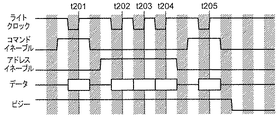
図2は、本実施形態のメモリシステムにおいてメモリコントローラ102がメモリ101からデータを読み出すにあたり、メモリコントローラ102からメモリ101に読み出しコマンドを発行する動作におけるタイミングチャートである。
FIG. 2 is a timing chart in the operation of issuing a read command from the
メモリコントローラ102は、コマンドイネーブル線111に“H”信号、アドレスイネーブル線112に“L”信号を出力している時、ライトクロック線113にライトクロックを出力する。また、メモリコントローラ102は、ライトクロックの立上りエッジのタイミングで、データ線115に、読み出し開始アドレスを指定するコマンドを出力する(t201)。
The
メモリコントローラ102は、その後、コマンドイネーブル線111に“H”信号、アドレスイネーブル線112に“L”信号を出力している時、ライトクロック線113にライトクロックを出力する。また、メモリコントローラ102は、ライトクロックの立上りエッジのタイミングで、時間t202、t203、t204で指定した読み出し対象アドレスのデータの出力を指示するコマンドをデータ線115に出力する(t205)。
Thereafter, the
メモリコントローラ102は、その後、コマンドイネーブル線111に“L”信号、アドレスイネーブル線112に“L”信号を出力している時、ライトクロック線113にライトクロックを出力する。また、メモリコントローラ102は、ライトクロックの立上りエッジのタイミングで、時間t202、t203、t204で指定した読み出し対象アドレスのデータの出力を指示するコマンドをデータ線115に出力する(t205)。
Thereafter, the
メモリ101は、t201〜t205のコマンド及びアドレスを受信すると、データ線に読み出し対象アドレスのデータを出力可能になるまでの間、ビジー線117にビジーの状態を表す“L”信号を出力する。メモリ101は、読み出しデータを出力可能になると、ビジー線117に“H”信号を出力する。そして、メモリ101は、メモリコントローラ102からリードクロック線114に出力されるリードクロックに同期して、データ線115に、読み出し対象アドレスのデータを出力する(図2には図示していない)。次に、この読み出し対象アドレスのデータの出力について、図3を参照して説明する。
When the
図3は、メモリシステムにおいてメモリ101がデータを出力する際の状態の一例を示すタイミングチャートである。
FIG. 3 is a timing chart showing an example of a state when the
メモリコントローラ102は、メモリ101からデータを読み出す際、リードクロック線114にリードクロックを出力する。
The
メモリ101は、リードクロック線114のリードクロックに同期してデータ線115にデータを出力する。
The
メモリ101は、時間t301のリードクロック1の立下りエッジを基準にして出力を開始したデータ1を、時間t303のリードクロック2の立下りエッジを基準にしてtROH(読み出し出力保持時間)後の時間t304までデータ線115に保持する(時間t304にデータ線115への出力を停止する)。メモリ101は、時間t303のリードクロック2の立下りエッジを基準にして、tREA時間後のt305までに、データ線115にデータ2の出力を開始する。したがって、本質的に次式の関係がある。
tROH<tREA
The
tROH <tREA
メモリ101は、時間t301のリードクロック1の立下りエッジを基準にして出力を開始したデータ1を、時間t303のリードクロック1の立下りエッジを基準にしてtROH(読み出し出力保持時間)後の時間t304までデータ線115に保持する(時間t304にデータ線115への出力を停止する)。メモリ101は、時間t303のリードクロックの立下りエッジを基準にして、tREA時間後のt305までに、データ線115にデータ2の出力を開始する。したがって、本質的に次式の関係がある。
tROH<tREA
The
tROH <tREA
ここで、本実施形態のメモリシステムにおいては、メモリ101は、リードクロックの立下りエッジを検出すると、アドレスをインクリメントし、インクリメントしたアドレスに対応するデータを出力する。換言すれば、連続したアドレスのデータを読み出す限り、アドレスを指定するコマンドを入力する必要はない。これにより、高速にデータを読み出すことが可能となる。
Here, in the memory system according to the present embodiment, when the falling edge of the read clock is detected, the
メモリ101は、時間t306の最後のリードクロック5の立下りエッジを基準にして、tREA後の時間t308までにデータ5の出力を開始する。メモリ101は、このデータ5を、時間t307のリードクロック5の立上りエッジを基準にしてtRHZ(読み出し出力高抵抗時間:データ線への出力を停止する時間)後のt309までデータ線115に保持する(t309にデータ線115への出力を停止する)。
The
メモリ101は、時間t306の最後のリードクロック5の立下りエッジを基準にして、tREA後の時間t308までにデータ5の出力を開始する。メモリ101は、このデータ4を、時間t307のリードクロック5の立上りエッジを基準にしてtRHZ(読み出し出力高抵抗時間:データ線への出力を停止する時間)後のt309までデータ線115に保持する(t309にデータ線115への出力を停止する)。
The
図4は、メモリコントローラ102の内部構成を示す図である。
FIG. 4 is a diagram illustrating an internal configuration of the
メモリコントローラ102は、制御回路401、クロック制御回路402、入力回路403、及びカウンタ404、及び出力回路405を備える。
The
制御回路401は、メモリコントローラ102全体を制御する。制御回路401は、コマンドを発行する期間を示す制御信号をコマンドイネーブル線111に出力する。制御回路401は、アドレスを指定する期間を示す制御信号をアドレスイネーブル線112に出力する。制御回路401は、ビジー線117からビジー信号を入力する。
The
クロック制御回路402は、コマンド、アドレス、及びメモリ101へのデータの転送タイミングを示す制御信号(ライトクロック)をライトクロック線113に出力する。クロック制御回路402は、メモリ101がデータを転送すべきタイミングを示す制御信号(リードクロック)をリードクロック線114に出力する。
The
制御回路401は、メモリ101からデータの読み出しを開始する際、読み出し対象の全データを所定数のデータでなるデータグループに分割しそのデータグループ単位で読み出す。制御回路401は、前記所定数をカウンタ404に設定する。
When the
入力回路403は、カウンタ404から最終データであることの通知を受けるまでは、戻りリードクロック線116の戻りリードクロックに同期して、データ線115からデータを取り込み、カウンタ404から最終データであることの通知を受けると、リードクロック線114のリードクロックに同期して、データ線115からデータを取り込む。
The
入力回路403は、カウンタ404から最終データであることの通知を受けるまでは、リードクロック線114のリードクロックに同期して、データ線115からデータを取り込み、カウンタから最終データであることの通知を受けると、戻りリードクロック線116の戻りリードクロックに同期して、データ線115からデータを取り込む。
The
出力回路405は、データ線115に、コマンドやアドレス等のデータを出力する。
The
図5は、クロック制御回路402の一部であって、リードクロック線114へのリードクロックの出力制御に関わる部分を示す回路図である。
FIG. 5 is a circuit diagram showing a part of the
この出力制御に関わる部分は、RSフリップフロップ501、Dフリップフロップ502,503、論理積回路504,505、Dフリップフロップ506、論理積回路(立下り検出回路)507、508を含む。
The part related to the output control includes an RS flip-
RSフリップフロップ501のセット端子Sには、リードクロック線114へのリードクロックの出力を開始すべきときに、制御回路401から、セット信号が入力される。RSフリップフロップ501のリセット端子Rには、リードクロック線114へのリードクロックの出力を終了すべきときに、カウンタ404から、リセット信号が入力される。RSフリップフロップ501は、セット端子Sにセット信号が入力されると“H”信号を出力し、リセット端子Rにリセット信号が入力されると“L”信号を出力する。
A set signal is input from the
論理積回路504には、RSフリップフロップ501の出力と、Dフリップフロップ506の出力、すなわちリードクロックが入力される。論理積回路504は、両入力が“H”のときのみ“L”信号を出力し、それ以外のときは“H”信号を出力する。
The AND
論理積回路505には、3つの論理積回路504、507,508の出力が入力される。論理積回路505は、3つの入力が全て“H”のときのみ“H”信号を出力し、それ以外のときは“L”信号を出力する。
The output of the three
論理積回路507には、RSフリップフロップ501の出力と、Dフリップフロップ502の出力が入力される。論理積回路507は、Dフリップフロップ502の出力が“H”,RSフリップフロップ501の出力が“L”のときのみ“L”信号を出力し、それ以外のときは“H”信号を出力する。
An output from the RS flip-
論理積回路508には、Dフリップフロップ502の出力と、Dフリップフロップ503の出力が入力される。論理積回路507は、Dフリップフロップ503の出力が“H”,Dフリップフロップ502の出力が“L”のときのみ“L”信号を出力し、それ以外のときは“H”信号を出力する。
The output of the D flip-
Dフリップフロップ502の入力Dには、RSフリップフロップ501の出力が入力される。Dフリップフロップ502は、クロック端子にクロック(サイクルタイムがリードクロックの1/2のクロック)が入力されたときにD端子に入力されている信号を、このクロックが入力されたときから次のクロックが入力されるまで出力する。
The output of the RS flip-
Dフリップフロップ503の入力Dには、Dフリップフロップ502の出力が入力される。Dフリップフロップ503は、クロック端子にクロック(サイクルタイムがリードクロックの1/2のクロック)が入力されたときにD端子に入力されている信号を、このクロックが入力されたときから次のクロックが入力されるまで出力する。
The output of the D flip-
Dフリップフロップ506の入力Dには、論理積回路505の出力が入力される。Dフリップフロップ506は、クロック端子にクロック(サイクルタイムがリードクロックの1/2のクロック)が入力されたときにD端子に入力されている信号を、このクロックが入力されたときから次のクロックが入力されるまで出力する。
The output of the AND
このような構成によれば、RSフリップフロップ501のセット端子Sにセット信号が入力されて、RSフリップフロップ501が“H”信号を出力すると、論理積回路507,508は上記セットと同時に“H”信号を出力する。また、RSフリップフロップ501のリセット端子Rにリセット信号が入力されて、RSフリップフロップ501が“L”信号を出力すると、論理積回路507はDフリップフロップ502の存在により1リードクロック分(リードクロックのサイクルタイムの1/2(tRC/2))遅れて“L”信号を出力し、論理積回路507は2つのDフリップフロップ502,503の存在により2リードクロック分(リードクロックの1サイクルタイム(tRC))遅れて“L”信号を出力する。
According to such a configuration, when a set signal is input to the set terminal S of the RS flip-
一方、論理積回路504は、RSフリップフロップ501のセット端子Sにセット信号が入力されて、RSフリップフロップ501から“H”信号が入力されると、セット時点では、リードクロックが出力されていないので、“H”信号を出力する。このとき、論理積回路505には、論理積回路507,508から“H”信号が入力されているので、論理積回路505は、“H”信号を出力する。そして、Dフリップフロップ506は、クロックが入力された時点で、“H”信号を出力する。すると、論理積回路504は、“L”信号を出力する。したがって、論理積回路505は、“L”信号を出力する。そして、Dフリップフロップ506は、クロックが入力された時点で“L”信号を出力する。すると、論理積回路504は、“H”信号を出力する。このように、Dフリップフロップ506にクロックが入力される都度、論理積回路504の出力が、“H”信号と“L”信号との間で切り替わり、その結果、Dフリップフロップ506からリードクロック線114に“H”信号と“L”信号とが交互に出力されることとなる。
On the other hand, when the set signal is input to the set terminal S of the RS flip-
一方、RSフリップフロップ501のリセット端子Sにリセット信号が入力されると、論理積回路504は“H”信号を出力するが、前述のように、論理積回路507はDフリップフロップ502の存在により1リードクロック分(リードクロックのサイクルタイムの1/2(tRC/2))遅れて“L”信号を出力し、論理積回路507は2つのDフリップフロップ502,503の存在により2リードクロック分(リードクロックの1サイクルタイム(tRC))遅れて“L”信号を出力する。したがって、論理積回路505は、RSフリップフロップ501のリセット端子Sにリセット信号が入力されるまでよりも、2リードクロック分(リードクロックの1サイクルタイム(tRC))長く“L”信号を出力する。すなわち、Dフリップフロップ506からリードクロック線114に“L”信号がそれまでよりも2リードクロック分(リードクロックの1サイクルタイム(tRC))長く出力されることとなる。
On the other hand, when a reset signal is input to the reset terminal S of the RS flip-
ここで、図中の511は、RSフリップフロップ501の出力信号を示しており、後で説明する図7に示すタイミングチャートにおいて利用する。
Here, 511 in the figure indicates an output signal of the RS flip-
なお、図5に示す回路は、メモリコントローラ102からリードクロック線114に出力する最後のリードクロックの“L”期間を長くするための回路の一例であり、同様の機能を実現できる限り図5で示した回路には限定されない。
Note that the circuit shown in FIG. 5 is an example of a circuit for extending the “L” period of the last read clock output from the
図6は、入力回路403の具体的構成を示す回路図である。
FIG. 6 is a circuit diagram showing a specific configuration of the
入力回路403は、Dフリップフロップ601,602,603,605、及びセレクタ604を備える。
The
Dフリップフロップ601の入力端子Dには、データ線115からデータが入力される。また、Dフリップフロップ601のクロック端子CLKには、戻りリードクロック線116から戻りリードクロックが入力される。Dフリップフロップ601は、クロック端子CLKに入力される戻りリードクロックの立下りエッジを検出したときに入力端子Dに入力されているデータを、この戻りリードクロックの立下りエッジが検出されたときから次の戻りリードクロックの立下りエッジが検出されるまで出力する。換言すれば、Dフリップフロップ601は、戻りリードクロックに同期して、入力端子Dに入力されているデータを出力する。
Data is input from the
Dフリップフロップ602の入力端子Dには、データ線115からデータが入力される。また、Dフリップフロップ602のクロック端子CLKには、リードクロック線114からリードクロックが入力される。Dフリップフロップ602は、クロック端子CLKに入力されるリードクロックの立上りエッジを検出したときに入力端子Dに入力されているデータを、このリードクロックの立上りエッジが検出されたときから次のリードクロックの立上りエッジが検出されるまで出力する。換言すれば、Dフリップフロップ602は、リードクロックに同期して、入力端子Dに入力されているデータを出力する。
Data is input from the
Dフリップフロップ603の入力端子Dには、Dフリップフロップ601の出力Qが入力される。また、Dフリップフロップ603のクロック端子CLKには、制御回路401の内部クロックが入力される。Dフリップフロップ603は、クロック端子CLKに制御回路401の内部クロックが入力されたときに入力端子Dに入力されているデータを、この内部クロックが入力されたときから次の内部クロックが入力されるまで出力する。換言すれば、Dフリップフロップ603は、制御回路401の内部クロックに同期して、入力端子Dに入力されているデータを出力する。
The output Q of the D flip-
セレクタ604は、カウンタ404からの信号に基づき、Dフリップフロップ602から出力されたデータまたはDフリップフロップ603から出力されたデータを選択的に出力する。具体的には、セレクタ604は、カウンタ404から最後のデータであることを示す信号を受けるまでは、Dフリップフロップ603からのデータを出力し、カウンタ404から最後のデータであることを示す信号を受けると、Dフリップフロップ602からのデータを出力する。
The
Dフリップフロップ605の入力端子Dには、セレクタ604から出力されたデータが入力される。また、Dフリップフロップ603のクロック端子CLKには、制御回路401の内部クロックが入力される。Dフリップフロップ605は、クロック端子CLKに制御回路401の内部クロックが入力されたときに入力端子Dに入力されているデータを、この内部クロックが入力されたときから次の内部クロックが入力されるまで出力する。換言すれば、Dフリップフロップ605は、制御回路401の内部クロックに同期して、入力端子Dに入力されているデータを制御回路401へ出力する。
The data output from the
このように、入力回路403は、カウンタ404から最終データであることの通知を受けるまでは、戻りリードクロック線116の戻りリードクロックに同期して、データ線115からデータを取り込み、カウンタ404から最終データであることの通知を受けると、リードクロック線114のリードクロックに同期して、データ線115からデータを取り込む。
In this manner, the
ここで図中の611〜615はDフリップフロップ601,602,603,605、及びセレクタ604の出力信号を示しており、後で説明する図7に示すタイミングチャートにおいて利用する。
Here,
なお、図6に示す回路は、データ線115にメモリ101から出力されるデータの取り込みタイミングとして2種類の取り込みタイミング(戻りリードクロック線116に同期したタイミングとリードクロック線114に同期したタイミング)で取り込む機能を備えた回路の一例である。同様の機能を実現できる限り図6で示した以外の回路を利用してもよい。
Note that the circuit shown in FIG. 6 has two types of capture timing (timing synchronized with the return read
図7は、メモリコントローラ102がメモリ101からデータを読み出すときの状態を示すタイミングチャートである。図7のタイミングチャートは、メモリコントローラ102がメモリ101から5ワードのデータを読み出す場合の例を示す。
FIG. 7 is a timing chart showing a state when the
まず時間t701で、メモリコントローラ102の制御回路401は、クロック制御回路402のRSフリップフロップ501にセット信号を出力する。これにより、RSフリップフロップ501の出力信号511は“H”になり、クロック制御回路402はリードクロック線114に“L”、“H”のトグル信号を出力する。また制御回路401は、RSフリップフロップ501にセット信号を出力するときに、カウンタ404に対してカウンタ404の初期値として読み出しワード数である5を設定する。
First, at time t <b> 701, the
カウンタ404は、リードクロックの立上りエッジに同期してカウンタをデクリメントする。
The
メモリ101からのデータの取り込みは、最終ワードを除き、戻りリードクロックの立下りのタイミングを基準として行われる。ここで特に認識しておくべきことは、1番目のデータの取り込みを行うために2番目の戻りリードクロックの立下りエッジを用いることである。同様にn番目のデータを取り込むためにはn+1番目のリードクロックをメモリ101に供給して、n+1番目の戻りリードクロックの立下りエッジを利用する。n+1番目のクロックをメモリ101に供給することは、メモリ101からのn+1番目のデータの出力を引き起こす。
Data fetch from the
メモリコントローラ102が、メモリ101からのデータの取り込みにおいてリードクロックを基準とせず戻りリードクロックを基準とする理由は以下の通りである。すなわち、メモリコントローラ102とメモリ101とを接続するリードクロック線114と接地間には容量成分が存在しており、この容量成分により、リードクロック線114上で伝送されるクロックには遅延が生じる。より高速な動作を行うためには、tREAよりも少し長い程度のtRCで制御を行う必要がある。そこで、戻りリードクロックを基準とし、遅延の影響を回避する。例えば、時間t704はリードクロックの立下りエッジのタイミングであるが、データ線115のデータ1を正しく取り込めるタイミングではないので、戻りリードクロックを利用する。
The reason why the
メモリ101は、5番目のデータ(データ5)を、5番目のリードクロックの立上り(時間t711)からtREAが経過した時点から、リードクロックの立上りのタイミング(時間t713)からtRHZ(図3参照)が経過するまでの間、データ線115に保持する(tRHZが経過したときにデータ線115への出力を停止する)。ここで、本実施形態では、上述のように5番目のリードクロックの“L”期間(出力期間(Tm2))を1〜4番目のリードクロックの“L”期間(出力期間(Tm1))よりも長くしているので(最後のリードクロックのサイクルタイムを長くしているので)、“L”期間(出力期間(Tm2)を長くしない場合よりも、5番目のデータ(データ5)をデータ線115に長い期間保持させることができる(出力可能とすることができる)。これにより、メモリコントローラ102がメモリ101からデータを取り込むことが可能な期間が増加することとなる。
The
メモリ101は、5番目のデータ(データ5)を、5番目のリードクロックの立上り(時間t711)からtREAが経過した時点から、リードクロックの立上りのタイミング(時間t713)からtRHZ(図3参照)が経過するまでの間、データ線115に保持する(tRHZが経過したときにデータ線115への出力を停止する)。ここで、本実施形態では、上述のように5番目のリードクロックの“L”期間(出力期間(Tm2))を1〜4番目のリードクロックの“L”期間(出力期間(Tm1))よりも長くしているので(最後のリードクロックのサイクルタイムを長くしているので)、“L”期間(出力期間(Tm2)を長くしない場合よりも、5番目のデータ(データ5)をデータ線115に長い期間保持させることができる(出力可能とすることができる)。これにより、メモリコントローラ102がメモリ102からデータを取り込むことが可能な期間が増加することとなる。
The
ここで、本実施の形態においては、5番目のリードクロックの“L”期間(Tm2)を、5番目のリードクロックの立上りのタイミングと、5番目のデータ(データ5)がデータ線115に保持されている期間とが時間軸上において重なるように設定している。これにより、Dフリップフロップ602は、5番目のデータ(データ5)がデータ線115に保持されている間に(tRHZが経過するまでの間に)、5番目のリードクロックの立上りを利用して、5番目のデータを取り込むことができる。
In the present embodiment, the “L” period (Tm2) of the fifth read clock is held in the
そして、カウンタ404は、カウンタの値を“1”から“0”にデクリメントすると同時に、入力回路403のセレクタ604への制御信号を“L”にする。セレクタ604は、カウンタ404からの制御信号が“L”なので、Dフリップフロップ602からのデータを出力する。Dフリップフロップ605は、セレクタ604から出力されたデータを、内部回路に同期して取り込み、制御回路401に出力する。
The
以上説明したように、本実施形態のメモリシステムによれば、メモリコントローラ102がメモリ101から連続してN個(本実施形態ではN=5)のデータを読み出す際、N番目のデータについてはN番目のリードクロックによるN番目のデータの出力開始後N番目のデータの出力停止までの間に取り込む。また、メモリコントローラ102は、N番目のリードクロックの出力期間を1番目からN−1番目のリードクロックの出力期間よりも長く設定する。これにより、“L”期間(出力期間(Tm2)を長くしない場合よりも、5番目のデータ(データ5)をデータ線115に長い期間保持させることができる(出力可能とすることができる)。つまり、メモリコントローラ102がメモリ101からデータを取り込むことが可能な期間が増加することとなる。本実施形態では、N番目のリードクロックの立上りのタイミングを、N番目のデータのデータ線115への出力可能な期間内に設定し、これにより、N番目のリードクロックの立上りを利用して、N番目のデータを取り込むようにしている。なお、N番目のデータのデータ線115への出力可能な期間内に、N番目のリードクロックの立上り以外の信号を利用して、N番目のデータを取り込むこともできる。例えば、N番目のリードクロックの立上り以外の信号として、例えばメモリコントローラ102内部のクロックを利用して生成したクロックや、N個目のリードクロックの立下りからtREA以上の所定時間が経過したときに発生させた任意の信号を利用することができる。
As described above, according to the memory system of the present embodiment, when the
以上説明したように、本実施形態のメモリシステムによれば、メモリコントローラ102がメモリ101から連続してN個(本実施形態ではN=5)のデータを読み出す際、N番目のデータについてはN番目のリードクロックによるN番目のデータの出力開始後N番目のデータの出力停止までの間に取り込む。また、メモリコントローラ102は、N番目のリードクロックの出力期間を1番目からN−1番目のリードクロックの出力期間よりも長く設定する。これにより、“L”期間(出力期間(Tm2)を長くしない場合よりも、5番目のデータ(データ5)をデータ線115に長い期間保持させることができる(出力可能とすることができる)。つまり、メモリコントローラ102がメモリ101からデータを取り込むことが可能な期間が増加することとなる。本実施形態では、N番目のリードクロックの立上りのタイミングを、N番目のデータのデータ線115への出力可能な期間内に設定し、これにより、N番目のリードクロックの立上りを利用して、N番目のデータを取り込むようにしている。なお、N番目のデータのデータ線115への出力可能な期間内に、N番目のリードクロックの立上り以外の信号を利用して、N番目のデータを取り込むこともできる。例えば、N番目のリードクロックの立上り以外の信号として、例えばメモリコントローラ11内部のクロックを利用して生成したクロックや、N個目のリードクロックの立下りからtREA以上の所定時間が経過したときに発生させた任意の信号を利用することができる。
As described above, according to the memory system of the present embodiment, when the
ここで、従来技術においては、N番目のデータを取り込むことはできない。また、この取り込めなかったデータを読み出そうとすると、改めて、アドレスを指定するコマンドやアドレスの指定をメモリコントローラ102からメモリ101に対して行う必要がある。つまり、読み出し対象のアドレスを指定するコマンドを発行する必要があるので、オーバヘッドが大きくなり、メモリシステムにおけるデータ転送の性能が低下していた。
Here, in the prior art, the Nth data cannot be captured. In addition, when trying to read the data that could not be captured, it is necessary to perform a command for designating an address or designation of the address from the
また、本実施形態のメモリシステムによれば、1番目のデータからN−1番目のデータについては戻りリードクロックに同期して取り込むので、メモリ101とメモリコントローラ102との間でリードクロックやデータの伝送に遅延が発生する場合でも、メモリから出力されたデータをメモリコントローラが取り込むことが可能となる。
Further, according to the memory system of the present embodiment, the N-1th data from the first data is fetched in synchronization with the return read clock, so that the read clock and the data between the
また、本実施形態のメモリシステムによれば、1番目のデータからN−1番目のデータについては戻りリードクロックに同期して取り込むので、メモリ101とメモリコントローラ101との間でリードクロックやデータの伝送に遅延が発生する場合でも、メモリから出力されたデータをメモリコントローラが取り込むことが可能となる。
Further, according to the memory system of the present embodiment, the N-1th data from the first data is fetched in synchronization with the return read clock, so that the read clock and data between the
なお、本実施形態では、1番目からN−1番目のデータについては1番目からN−1番目(上記例では5番目)の戻りリードクロックの立下りに同期して取り込むようにしたが、遅延時間が小さい場合は、戻りリードクロックでなくリードクロックの立下りに同期して1番目からN−1番目のデータを取り込むようにしてもよい。この場合、戻りリードクロック線116を設けなくてもよい。
In the present embodiment, the 1st to (N-1) th data is fetched in synchronization with the fall of the 1st to (N-1) th (5th in the above example) return read clock. When the time is short, the first to (N-1) th data may be fetched in synchronization with the fall of the read clock instead of the return read clock. In this case, the return read
また、本実施形態では、メモリ101は、N個のデータを出力する際、1番目からN番目のリードクロックの立下りエッジ(出力開始時のエッジ)を基準として出力を開始するが、1番目からN番目のリードクロックの立上りエッジ(出力完了時のエッジ)を基準としてもよい。また、メモリ101は、1番目からN−1番目のデータについてはそれぞれ2番目からN番目のリードクロックの立下りエッジ(出力開始時のエッジ)を基準として出力を停止するが、2番目からN番目のリードクロックの立上りエッジ(出力完了時のエッジ)を基準としてもよい(但し、2番目からN番目のリードクロックの立上りエッジ(出力完了時のエッジ)よりも後までデータが出力されているとき)。また、メモリコントローラ102は、1番目からN−1番目のデータについては2番目からN番目のリードクロックの立下りエッジ(出力開始時のエッジ)に同期して取り込むが、データがデータ線115に出力されるタイミングによっては、2番目からN番目のリードクロックの立上りエッジ(出力完了時のエッジ)に同期して取り込んでもよい。また、本実施形態では、リードクロックは立下りクロックであるが、立上りクロックであってもよく、この場合、出力開始時のエッジは立上りエッジ、出力完了時のエッジは立下りエッジとして制御すればよい。
In this embodiment, the
本実施形態では、説明を簡略化するために、メモリから読み出すデータの塊に含まれるデータの数NがN=5の場合について説明したが、データの塊に含まれるデータの数NはN=5に限定されるものではない。メモリからデータを読み出す際のデータの塊にはECC符号を含めてもよい。この場合にメモリから読み出すデータの塊のサイズは、メモリコントローラが取り扱うデータのサイズにECC符号のサイズを付与したサイズとなる。例えば、データのサイズが512バイト、ECC符号のサイズが16バイトとした場合、データの塊のサイズは528バイトとなる。このようにデータの塊にECC符号を含めることにより、メモリからデータの塊を読み出す毎にメモリコントローラによるECC処理が行える。これは、ECC処理を容易化できる。なお、Nを例えばメモリシステムのバッファ容量等に応じて可変としてもよく、その場合においても本実施形態の技術思想は適用可能である。 In the present embodiment, in order to simplify the description, the case where the number N of data included in the data chunk read from the memory is N = 5 has been described. However, the number N of data included in the data chunk is N = It is not limited to five. An ECC code may be included in the data chunk when data is read from the memory. In this case, the size of the data chunk read from the memory is a size obtained by adding the size of the ECC code to the size of the data handled by the memory controller. For example, if the data size is 512 bytes and the ECC code size is 16 bytes, the data chunk size is 528 bytes. By including the ECC code in the data chunk in this way, the ECC processing by the memory controller can be performed every time the data chunk is read from the memory. This can facilitate ECC processing. Note that N may be variable according to, for example, the buffer capacity of the memory system, and the technical idea of the present embodiment is also applicable in this case.
本発明は、メモリシステムにおけるデータ転送の効率を向上して高速化することが可能なユーザ利便性の高いメモリシステムに有用である。 INDUSTRIAL APPLICABILITY The present invention is useful for a user-friendly memory system capable of improving the speed of data transfer in the memory system and increasing the speed.
101 メモリ
102 メモリコントローラ
111 コマンドイネーブル線
112 アドレスイネーブル線
113 ライトクロック線
114 リードクロック線
115 データ線
116 戻りリードクロック線
117 ビジー線
401 制御回路
402 クロック制御回路
403 入力回路
404 カウンタ
405 出力回路
101
Claims (12)
前記メモリインターフェースは、データの転送を行うために前記メモリが駆動するデータ線と、前記メモリから前記データ線へのデータ出力のタイミングを制御するためのリードクロックが伝送され、前記メモリコントローラが駆動するクロック線とを含み、
前記メモリは、N個のデータを出力する際、前記メモリコントローラから連続的に出力される1番目からN番目のリードクロックに同期して出力を開始し、1番目からN−1番目のデータについては2番目からN番目のリードクロックにそれぞれ同期して出力を停止し、N番目のデータについてはN番目のリードクロックの出力停止から第1の所定時間経過後に出力を停止し、
前記メモリコントローラは、1番目からN−1番目のデータについては2番目からN番目のリードクロックにそれぞれ同期して取り込み、N番目のデータについてはN番目のリードクロックによるN番目のデータの出力開始後N番目のデータの出力停止までの間に取り込み、N番目のリードクロックの出力期間を1番目からN−1番目のリードクロックの出力期間よりも長く設定することを特徴とするメモリシステム。 A memory system including a memory, a memory controller, and a memory interface that electrically connects the memory and the memory controller,
The memory interface is driven by the memory controller by transmitting a data line driven by the memory to transfer data and a read clock for controlling timing of data output from the memory to the data line. Including clock lines,
When outputting N data, the memory starts outputting in synchronization with the 1st to Nth read clocks continuously output from the memory controller, and the 1st to (N-1) th data. Stops outputting in synchronization with the second to Nth read clocks, and stops outputting the Nth data after the first predetermined time has elapsed since the output of the Nth read clock was stopped,
The memory controller fetches the 1st to (N-1) th data in synchronization with the 2nd to Nth read clocks, and starts the output of the Nth data with the Nth read clock for the Nth data. A memory system wherein the N-th read clock is output before the output of the N-th data is stopped and the output period of the N-th read clock is set longer than the output period of the first to (N-1) -th read clock.
前記メモリインターフェースは、データの転送を行うために前記メモリが駆動するデータ線と、前記メモリから前記データ線へのデータ出力のタイミングを制御するためのリードクロックが伝送され、前記メモリコントローラが駆動するクロック線と、前記クロック線を介して前記メモリに到達したリードクロックを前記メモリコントローラに、戻りリードクロックとして戻す戻りクロック線とを含み、
前記メモリは、N個のデータを出力する際、前記メモリコントローラから連続的に出力される1番目からN番目のリードクロックに同期して出力を開始し、1番目からN−1番目のデータについては2番目からN番目のリードクロックにそれぞれ同期して出力を停止し、N番目のデータについてはN番目のリードクロックの出力停止から第1の所定時間経過後に出力を停止し、
前記メモリコントローラは、1番目からN−1番目のデータについては2番目からN番目の戻りリードクロックにそれぞれ同期して取り込み、N番目のデータについてはN番目のリードクロックによるN番目のデータの出力開始後N番目のデータの出力停止までの間に取り込み、N番目のリードクロックの出力期間を1番目からN−1番目のリードクロックの出力期間よりも長く設定することを特徴とするメモリシステム。 A memory system including a memory, a memory controller, and a memory interface that electrically connects the memory and the memory controller,
The memory interface is driven by the memory controller by transmitting a data line driven by the memory to transfer data and a read clock for controlling timing of data output from the memory to the data line. A clock line, and a return clock line that returns a read clock that has reached the memory via the clock line to the memory controller as a return read clock,
When outputting N data, the memory starts outputting in synchronization with the 1st to Nth read clocks continuously output from the memory controller, and the 1st to (N-1) th data. Stops outputting in synchronization with the second to Nth read clocks, and stops outputting the Nth data after the first predetermined time has elapsed since the output of the Nth read clock was stopped,
The memory controller captures the 1st to (N-1) th data in synchronization with the 2nd to Nth return read clocks, and outputs the Nth data for the Nth data by the Nth read clock. A memory system, wherein the output period of the Nth read clock is set after the start and the output period of the Nth read clock is set longer than the output period of the first to (N-1) th read clocks.
Priority Applications (1)
| Application Number | Priority Date | Filing Date | Title |
|---|---|---|---|
| JP2010121728A JP5449032B2 (en) | 2009-05-28 | 2010-05-27 | Memory system |
Applications Claiming Priority (3)
| Application Number | Priority Date | Filing Date | Title |
|---|---|---|---|
| JP2009128461 | 2009-05-28 | ||
| JP2009128461 | 2009-05-28 | ||
| JP2010121728A JP5449032B2 (en) | 2009-05-28 | 2010-05-27 | Memory system |
Publications (3)
| Publication Number | Publication Date |
|---|---|
| JP2011008779A JP2011008779A (en) | 2011-01-13 |
| JP2011008779A5 JP2011008779A5 (en) | 2013-07-04 |
| JP5449032B2 true JP5449032B2 (en) | 2014-03-19 |
Family
ID=43301613
Family Applications (1)
| Application Number | Title | Priority Date | Filing Date |
|---|---|---|---|
| JP2010121728A Expired - Fee Related JP5449032B2 (en) | 2009-05-28 | 2010-05-27 | Memory system |
Country Status (2)
| Country | Link |
|---|---|
| US (1) | US8375238B2 (en) |
| JP (1) | JP5449032B2 (en) |
Families Citing this family (3)
| Publication number | Priority date | Publication date | Assignee | Title |
|---|---|---|---|---|
| KR101188264B1 (en) * | 2010-12-01 | 2012-10-05 | 에스케이하이닉스 주식회사 | Semiconductor System, Semiconductor Memory Apparatus, and Method for Input/Output of Data Using the Same |
| US10083137B2 (en) * | 2015-04-02 | 2018-09-25 | Atmel Corporation | Peripheral interface circuit for serial memory |
| US11854602B2 (en) * | 2021-12-08 | 2023-12-26 | Advanced Micro Devices, Inc. | Read clock start and stop for synchronous memories |
Family Cites Families (12)
| Publication number | Priority date | Publication date | Assignee | Title |
|---|---|---|---|---|
| IL96808A (en) * | 1990-04-18 | 1996-03-31 | Rambus Inc | Integrated circuit i/o using a high performance bus interface |
| JPH05298241A (en) * | 1992-04-23 | 1993-11-12 | Meidensha Corp | Burst transfer system |
| JP3276798B2 (en) * | 1995-02-02 | 2002-04-22 | 株式会社日立国際電気 | Method and apparatus for displaying waveform in digital oscilloscope |
| JP2003140962A (en) * | 2001-10-30 | 2003-05-16 | Mitsubishi Electric Corp | Signal transmit/receive system |
| JP2002304323A (en) * | 2002-02-04 | 2002-10-18 | Hitachi Ltd | Information processing device |
| JP2003257200A (en) * | 2002-03-01 | 2003-09-12 | Mitsubishi Electric Corp | Semiconductor memory device |
| EP1501100B1 (en) * | 2003-07-22 | 2018-11-28 | Samsung Electronics Co., Ltd. | Nonvolatile memory device, memory system, and operating methods |
| KR100546418B1 (en) * | 2004-07-27 | 2006-01-26 | 삼성전자주식회사 | Non-volatile memory device performing double data rate operation in reading operation and method thereof |
| JP2006277892A (en) | 2005-03-30 | 2006-10-12 | Elpida Memory Inc | Semiconductor memory device |
| KR101458381B1 (en) * | 2006-04-24 | 2014-11-07 | 샌디스크 테크놀로지스, 인코포레이티드 | High-performance flash memory data transfer |
| JP4267002B2 (en) * | 2006-06-08 | 2009-05-27 | エルピーダメモリ株式会社 | System with controller and memory |
| US8015382B1 (en) * | 2007-02-28 | 2011-09-06 | Altera Corporation | Method and apparatus for strobe-based source-synchronous capture using a first-in-first-out unit |
-
2010
- 2010-05-27 US US12/788,740 patent/US8375238B2/en active Active
- 2010-05-27 JP JP2010121728A patent/JP5449032B2/en not_active Expired - Fee Related
Also Published As
| Publication number | Publication date |
|---|---|
| JP2011008779A (en) | 2011-01-13 |
| US20100313055A1 (en) | 2010-12-09 |
| US8375238B2 (en) | 2013-02-12 |
Similar Documents
| Publication | Publication Date | Title |
|---|---|---|
| EP1807766B1 (en) | De-coupled memory access system and method | |
| US8687451B2 (en) | Power management in semiconductor memory system | |
| US8547760B2 (en) | Memory access alignment in a double data rate (‘DDR’) system | |
| KR100907016B1 (en) | Data input circuit of semiconductor memory apparatus and control method of the same | |
| JP5655555B2 (en) | MEMORY INTERFACE CIRCUIT, MEMORY INTERFACE METHOD, AND ELECTRONIC DEVICE | |
| US10970243B2 (en) | Front end serial bus automatic bus park tri-state activation | |
| US20090216926A1 (en) | Apparatus to improve bandwidth for circuits having multiple memory controllers | |
| US9026746B2 (en) | Signal control device and signal control method | |
| KR20180113371A (en) | Data storage device | |
| US10846021B2 (en) | Memory devices with programmable latencies and methods for operating the same | |
| JP5449032B2 (en) | Memory system | |
| US9183900B2 (en) | Data paths using a first signal to capture data and a second signal to output data and methods for providing data | |
| US20220245077A1 (en) | Integrated circuit and system control device including same | |
| US20190258400A1 (en) | Memory devices configured to latch data for output in response to an edge of a clock signal generated in response to an edge of another clock signal | |
| US7706195B2 (en) | Strobe signal controlling circuit | |
| JP2011008779A5 (en) | ||
| US8320204B2 (en) | Memory interface control circuit | |
| US20130054937A1 (en) | Apparatuses and methods for providing data from multiple memories | |
| JP2011181029A (en) | Data transfer control device | |
| JP5489871B2 (en) | Image processing device | |
| US8429438B2 (en) | Method and apparatus for transferring data between asynchronous clock domains | |
| US6810098B1 (en) | FIFO read interface protocol | |
| US7827455B1 (en) | System and method for detecting glitches on a high-speed interface | |
| CN115035929A (en) | Circuit, method and electronic equipment for efficiently realizing clock domain crossing of pseudo DDR signal | |
| WO2006112968A1 (en) | Apparatus to improve bandwidth for circuits having multiple memory controllers |
Legal Events
| Date | Code | Title | Description |
|---|---|---|---|
| A521 | Request for written amendment filed |
Free format text: JAPANESE INTERMEDIATE CODE: A523 Effective date: 20130517 |
|
| A621 | Written request for application examination |
Free format text: JAPANESE INTERMEDIATE CODE: A621 Effective date: 20130517 |
|
| A977 | Report on retrieval |
Free format text: JAPANESE INTERMEDIATE CODE: A971007 Effective date: 20131120 |
|
| TRDD | Decision of grant or rejection written | ||
| A01 | Written decision to grant a patent or to grant a registration (utility model) |
Free format text: JAPANESE INTERMEDIATE CODE: A01 Effective date: 20131126 |
|
| A61 | First payment of annual fees (during grant procedure) |
Free format text: JAPANESE INTERMEDIATE CODE: A61 Effective date: 20131224 |
|
| R150 | Certificate of patent or registration of utility model |
Ref document number: 5449032 Country of ref document: JP Free format text: JAPANESE INTERMEDIATE CODE: R150 Free format text: JAPANESE INTERMEDIATE CODE: R150 |
|
| LAPS | Cancellation because of no payment of annual fees |