JP5439707B2 - Signal processing apparatus and signal processing method - Google Patents
Signal processing apparatus and signal processing method Download PDFInfo
- Publication number
- JP5439707B2 JP5439707B2 JP2007105711A JP2007105711A JP5439707B2 JP 5439707 B2 JP5439707 B2 JP 5439707B2 JP 2007105711 A JP2007105711 A JP 2007105711A JP 2007105711 A JP2007105711 A JP 2007105711A JP 5439707 B2 JP5439707 B2 JP 5439707B2
- Authority
- JP
- Japan
- Prior art keywords
- signal processing
- signal
- digital
- filter
- noise
- Prior art date
- Legal status (The legal status is an assumption and is not a legal conclusion. Google has not performed a legal analysis and makes no representation as to the accuracy of the status listed.)
- Expired - Fee Related
Links
Images


Description
本発明は、音声信号を対象として所定目的に応じた信号処理を実行するようにされた、信号処理装置と、その方法に関するものである。 The present invention relates to a signal processing apparatus and a method for performing signal processing according to a predetermined purpose on an audio signal.
ヘッドフォン装置により楽曲などのコンテンツの音声を再生しているときに聴こえてくる外部のノイズをアクティブにキャンセルするようにされた、ヘッドフォン装置対応のいわゆるノイズキャンセリングシステムが知られ、また、実用化されるようになってきている。そして、このようなノイズキャンセリングシステムとしては、大別してフィードバック方式とフィードフォワード方式との2つの方式が知られている。 A so-called noise canceling system for headphone devices that actively cancels external noise that is heard when playing sound of content such as music with a headphone device is known and put into practical use. It is becoming. And as such a noise canceling system, two systems, a feedback system and a feedforward system, are roughly classified.
例えば、特許文献1には、ユーザの耳に装着される音響管内においてイヤホンユニットの近傍に設けたマイクロフォンユニットにより収音した音響管内部の騒音(ノイズ)を位相反転させた音声信号を生成し、これをイヤホンユニットから音として出力させることにより、外部ノイズを低減させるようにした構成、つまり、フィードバック方式に対応したノイズキャンセリングシステムの構成が記載されている。
また、特許文献2には、その基本構成として、ヘッドフォン装置外筐に取り付けたマイクロフォンにより収音して得た音声信号について所要の伝達関数による特性を与えてヘッドフォン装置から出力させるようにした構成、つまりフィードフォワード方式に対応したノイズキャンセリングシステムの構成が記載されている。
For example,
Further, in
ところで、上記したフィードバック方式とフィードフォワード方式との何れについてもいえることであるが、現在、民生機器におけるヘッドフォン装置のノイズキャンセリングシステムとして実用化されているものは、アナログ回路により構成されたものとなっている。
ノイズキャンセリングシステムのノイズキャンセル効果が有効に得られるようにするためには、例えばマイクロフォンにより収音された外部の不要音と、この不要音のキャンセルのためにドライバから出力される音との位相差を一定以内に納めることが必要である。換言すれば、ノイズキャンセリングシステムにおいて、外部の不要音を入力してから、これに応じたキャンセル音が出力されるまでの速度(応答速度)が一定以内であることが要求される。
しかしながら、ノイズキャンセリングシステムをデジタル回路により構成しようとすると、その入力と出力にA/Dコンバータ、D/Aコンバータを備えることになる。現状で広く用いられるA/Dコンバータ、D/Aコンバータの処理時間では、ノイズキャンセリングシステムとしての採用を考えた場合には遅延が相当に大きく、有効なノイズキャンセル効果を得ることが難しい。例えば、軍事用、産業用などの分野では、サンプリング周波数が相当に高くて遅延の少ないA/Dコンバータ、D/Aコンバータが存在するが、これらは著しく高価であり、民生機器で採用することは現実的ではない。現状にあってノイズキャンセリングシステムをデジタル回路により構成せずに、アナログ回路により構成しているのは、このような理由による。
By the way, although it can be said about both the above-mentioned feedback system and feedforward system, what is currently put into practical use as a noise canceling system for a headphone device in a consumer device is configured by an analog circuit. It has become.
In order to effectively obtain the noise canceling effect of the noise canceling system, for example, the relationship between the external unnecessary sound collected by the microphone and the sound output from the driver for canceling the unnecessary sound is compared. It is necessary to keep the phase difference within a certain range. In other words, in the noise canceling system, a speed (response speed) from when an external unnecessary sound is input to when a canceling sound according to the input is output is required to be within a certain range.
However, if the noise canceling system is configured by a digital circuit, an A / D converter and a D / A converter are provided at the input and output. In the processing time of A / D converters and D / A converters that are widely used at present, when adopting as a noise canceling system, the delay is considerably large and it is difficult to obtain an effective noise canceling effect. For example, in the military and industrial fields, there are A / D converters and D / A converters that have a considerably high sampling frequency and a small delay, but these are extremely expensive and are not used in consumer equipment. Not realistic. This is the reason why the noise canceling system is configured by an analog circuit instead of a digital circuit.
とはいえ、アナログ回路をデジタル回路に置き換えることによっては、物理的な部品素子の定数の変更、交換などを行うことなく、特性や動作モードの変更、切り換えを行うことが容易化されるものであり、また、ノイズキャンセリングシステムのような音響に関連したシステムであれば、さらなる音質の向上も期待できるなど、利点は多い。
そこで、本願発明としては、例えば民生におけるヘッドフォン装置のノイズキャンセリングシステムなどとして、デジタル回路により形成したものでありながら、実用上、充分なノイズキャンセル効果が得られるようにすることを目的とする。
However, replacing analog circuits with digital circuits facilitates changing and switching characteristics and operating modes without changing or replacing physical component element constants. In addition, there are many advantages that a sound-related system such as a noise canceling system can be expected to further improve sound quality.
Accordingly, an object of the present invention is to provide a practically sufficient noise canceling effect while being formed by a digital circuit, for example, as a noise canceling system for a headphone device in a consumer.
そこで本発明は上記した課題を考慮して、信号処理装置として次のように構成する。
つまり、ΔΣ変調処理により得られる1ビット以上の所定の量子化ビット数による第1の形式のデジタル信号を入力して、所定の基準サンプリング周波数をfsとしてn×fs(nは自然数)で表されるサンプリング周波数によるパルスコード変調信号とされる第2の形式のデジタル信号を生成して出力する第1のデシメーション処理手段と、上記第1のデシメーション処理手段から出力される第2の形式のデジタル信号を入力して、m×fs(mは自然数、かつ、m<n)で表されるサンプリング周波数によるパルスコード変調信号としての形式を有する第3の形式のデジタル信号を生成して出力する第2のデシメーション処理手段と、上記第2のデシメーション処理手段から出力される第3の形式のデジタル信号を入力して所定の機能目的に応じた所定の信号処理を実行し、同じ第3の形式により出力するようにされた第1の機能対応信号処理手段と、上記第1の機能対応信号処理手段から出力される第3の形式の信号を、第2の形式に変換して出力するようにされたインターポレーション処理手段と、上記第1のデシメーション処理手段から出力される第2の形式のデジタル信号を入力して上記機能目的に応じた所定の信号処理を実行し、同じ第2の形式により出力するようにされた第2の機能対応信号処理手段と、少なくとも、上記第2の機能対応信号処理手段から出力される第2の形式のデジタル信号と、上記インターポレーション処理手段から出力される第2の形式のデジタル信号とを、少なくとも合成し、後段のデジタル−アナログ変換処理のための入力段に対して出力する合成手段とを備え、上記第1の機能対応信号処理手段は、上記機能目的に応じた所定の信号処理として、中域及び低域とされる所定以下の周波数帯域または、低域とされる所定以下の周波数帯域のキャンセル対象音をキャンセルするためのキャンセル信号特性を与えるための信号処理を実行するように構成され、上記第1の機能対応信号処理手段を、中域及び低域とされる所定以下の周波数帯域のキャンセル対象音成分がキャンセルされるようにするための信号特性を与えるようにフィルタ特性を設定する場合には、上記第2の機能対応信号処理手段を、上記中域及び低域よりも高いとされる周波数帯域のキャンセル対象音成分がキャンセルされるようにするための信号特性を与えるようにフィルタ特性を設定し、記第2の機能対応信号処理手段は、直線位相型の有限インパルス応答システムのデジタルフィルタにより構成し、または、上記第1の機能対応信号処理手段を、低域とされる所定以下の周波数帯域のキャンセル対象音成分がキャンセルされるようにするためのキャンセル信号特性を与えるようにフィルタ特性を設定する場合には、上記第2の機能対応信号処理手段を、上記低域よりも高いとされる周波数帯域のキャンセル対象音成分がキャンセルされるようにするための信号特性を与えるようにフィルタ特性を設定し、上記第2の機能対応信号処理手段は、無限インパルス応答システムのデジタルフィルタにより構成することとした。
In view of the above-described problems, the present invention is configured as a signal processing apparatus as follows.
That is, a digital signal of the first format having a predetermined quantization bit number of 1 bit or more obtained by ΔΣ modulation processing is input, and expressed as n × fs (n is a natural number) with a predetermined reference sampling frequency as fs. First decimation processing means for generating and outputting a digital signal of the second format that is a pulse code modulated signal with a sampling frequency of the second, and a digital signal of the second format that is output from the first decimation processing means To generate and output a digital signal of the third format having a format as a pulse code modulation signal with a sampling frequency represented by m × fs (m is a natural number and m <n) Decimation processing means and a third format digital signal output from the second decimation processing means, and a predetermined signal corresponding to a predetermined functional purpose. A first function-corresponding signal processing means configured to execute the process and output in the same third format; and a third format signal output from the first function-corresponding signal processing means; An interpolation processing means that is converted into a format of the output and a second format digital signal output from the first decimation processing means and a predetermined signal corresponding to the functional purpose A second function-corresponding signal processing means configured to execute processing and output in the same second format; and at least a second format digital signal output from the second function-corresponding signal processing means; And a synthesizing means for synthesizing at least a digital signal of the second format output from the interpolation processing means and outputting it to the input stage for the subsequent digital-analog conversion process. The first function-compatible signal processing means includes a predetermined frequency band corresponding to the functional purpose, a predetermined frequency band that is a low frequency range, or a predetermined frequency band that is a low frequency range. A signal processing for giving a cancellation signal characteristic for canceling the cancellation target sound is performed, and the first function-corresponding signal processing means is set to a mid-range and low-frequency range below a predetermined frequency band. When the filter characteristic is set so as to give a signal characteristic for canceling the cancellation target sound component, the second function corresponding signal processing means is higher than the middle range and the low range. canceled target sound components of the frequency band set the filter characteristics to provide a signal characteristic of the order to be canceled is, serial second function corresponding signal processing means, the straight line A digital filter of a phase type finite impulse response system, or the first function corresponding signal processing means for canceling a cancellation target sound component in a frequency band below a predetermined frequency which is a low frequency range When the filter characteristic is set so as to give the cancellation signal characteristic, the second function corresponding signal processing means cancels the cancel target sound component in the frequency band higher than the low frequency band. The filter characteristic is set so as to give the signal characteristic to achieve the above, and the second function corresponding signal processing means is constituted by a digital filter of an infinite impulse response system.
上記構成では、所定のキャンセル対象音をキャンセル(低減、減衰)するシステムのデジタル信号処理系について、m×fsのサンプリング周波数の信号に所定のキャンセル対象音をキャンセルするための信号特性(キャンセル信号特性)を与える系と、これより高いサンプリング周波数n×fsの信号にキャンセル信号特性を与える系との、複数の系が備えられる。そのうえで、後者のサンプリング周波数n×fsの信号にキャンセル信号特性を与える系においては、第2のデシメーション処理手段によるデシメーションと、インターポレーション処理手段によるインターポレーション処理が施されることなく、合成器において、前者のキャンセル信号特性が与えられたサンプリング周波数n×fsの信号と合成される。このようにして、デシメーション処理とインターポレーション処理が省略されることによって、後者の系の信号の遅延は大幅に短縮されることになる。 In the above configuration, for a digital signal processing system of a system that cancels (reduces or attenuates) a predetermined cancellation target sound, a signal characteristic (cancellation signal characteristic) for canceling the predetermined cancellation target sound to a signal having a sampling frequency of m × fs. ) And a system that provides a cancellation signal characteristic to a signal having a higher sampling frequency n × fs. In addition, in the latter system that gives the cancel signal characteristic to the signal of the sampling frequency n × fs, the synthesizer is not subjected to the decimation by the second decimation processing means and the interpolation processing by the interpolation processing means. 2 is synthesized with a signal of sampling frequency n × fs given the cancel signal characteristic of the former. Thus, by omitting the decimation process and the interpolation process, the signal delay of the latter system is greatly reduced.
上記のようにして、複数のキャンセル信号特性を与える系を備えたうえで、そのうちの少なくとも1つの系における信号遅延(信号伝搬時間)が短いものとされることで、システム全体として、例えばヘッドフォン装置のノイズキャンセリングシステムの信号処理系に要求される応答速度の条件を満たすことができる。つまり、デジタル回路方式によるノイズキャンセリングシステムを容易に実現することが可能となる。そして、デジタル回路によるノイズキャンセリングシステムが実現されることで、アナログ回路によるものでは困難であった機能の実装であるとか、高音質化などが図られることになるものであり、ユーザにとっての利用価値は高まる。
また、本願発明のようにして、キャンセル信号特性を与える系を複数備えていることで、例えば各系に特定の信号処理的な機能を割り当てて分担させるなどすることが可能であり、ノイズキャンセリングシステムとしての性能向上、設計自由度の向上なども図られることになる。
As described above, a system that provides a plurality of cancel signal characteristics is provided, and a signal delay (signal propagation time) in at least one of the systems is shortened. The response speed required for the signal processing system of the noise canceling system can be satisfied. That is, it becomes possible to easily realize a noise canceling system using a digital circuit method. The realization of a noise-cancelling system using digital circuits will enable the implementation of functions that have been difficult with analog circuits, and improve sound quality. Value increases.
Further, as in the present invention, by providing a plurality of systems that give cancel signal characteristics, for example, it is possible to assign a specific signal processing function to each system and share it, and noise canceling System performance and design flexibility will be improved.
本願発明を実施するための最良の形態(以下、実施の形態という)としては、ノイズキャンセリングシステムが搭載されたヘッドフォン装置を例に挙げることとする。
そこで、本実施の形態としての構成を説明するのに先立ち、ヘッドフォン装置に対応するノイズキャンセリングシステムの基本概念について説明を行っておくこととする。
As a best mode for carrying out the present invention (hereinafter referred to as an embodiment), a headphone device equipped with a noise canceling system is taken as an example.
Therefore, prior to describing the configuration of the present embodiment, the basic concept of a noise canceling system corresponding to a headphone device will be described.
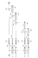
このようなヘッドフォン装置対応のノイズキャンセリングシステムの基本的な方式としては、フィードバック方式によりサーボ制御を行うようにされたものとフィードフォワード方式がそれぞれ知られている。先ず、図1により、フィードバック方式について説明する。 As a basic method of such a noise canceling system compatible with a headphone device, a servo control by a feedback method and a feedforward method are respectively known. First, the feedback system will be described with reference to FIG.
図1(a)には、ヘッドフォン装着者(ユーザ)の右耳(L(左),R(右)による2チャンネルステレオにおけるRチャンネル)側における、フィードバック方式によるノイズキャンセリングシステムのモデル例を模式的に示している。
ここでのヘッドフォン装置のRチャンネル側の構造としては、先ず、右耳に対応するハウジング部201内において、ヘッドフォン装置を装着したユーザ500の右耳に対応する位置にドライバ202を設けるようにされる。ドライバ202は、いわゆるスピーカと同義のものであり、音声信号の増幅出力により駆動(ドライブ)されることで音声を空間に放出するようにして出力するものである。
FIG. 1A schematically shows a model example of a noise canceling system using a feedback method on the right ear (R channel in two-channel stereo by L (left) and R (right)) of a headphone wearer (user). Is shown.
As a structure on the R channel side of the headphone device here, first, a driver 202 is provided in a position corresponding to the right ear of the user 500 wearing the headphone device in the housing portion 201 corresponding to the right ear. . The driver 202 is synonymous with a so-called speaker, and is driven (driven) by an amplified output of an audio signal so as to output the sound so as to be released into the space.
そのうえで、フィードバック方式としては、ハウジング部201内においてユーザ500の右耳に近いとされる位置に対してマイクロフォン203を設けるようにされる。このようにして設けられるマイクロフォン203によっては、ドライバ202から出力される音声と、外部のノイズ音源301からハウジング部201内に侵入して右耳に到達しようとする音声、つまり右耳にて聴き取られる外部音声であるハウジング内ノイズ302とが収音されることになる。なお、ハウジング内ノイズ302が発生する原因としては、ノイズ音源301が例えばハウジング部のイヤーパッドなどの隙間から音圧として漏れてきたり、ヘッドフォン装置の筐体がノイズ音源301の音圧を受けて振動し、これがハウジング部内に伝達されてくることなどを挙げることができる。
そして、マイクロフォン203によって収音して得られた音声信号から、例えば外部音声の音声信号成分に対して逆特性となる信号など、ハウジング内ノイズ302がキャンセル(減衰、低減)されるようにするための信号(キャンセル用オーディオ信号)を生成し、この信号について、ドライバ202を駆動する必要音の音声信号(オーディオ音源)に合成させるようにして帰還させる。これによりハウジング部201内における右耳に対応するとされる位置に設定されたノイズキャンセル点400においては、ドライバ202からの出力音声と外部音声の成分とが合成されることによって外部音声がキャンセルされた音が得られ、ユーザの右耳では、この音を聴き取ることになる。そして、このような構成を、Lチャンネル(左耳)側においても与えることで、通常のL,R2チャンネルステレオに対応するヘッドフォン装置としてのノイズキャンセリングシステムが得られることになる。
In addition, as a feedback method, the
Then, in order to cancel (attenuate or reduce) the in-housing noise 302 such as a signal having a reverse characteristic with respect to the audio signal component of the external audio from the audio signal obtained by collecting the sound with the
図1(b)のブロック図は、フィードバック方式によるノイズキャンセリングシステムの基本的なモデル構成例を示している。なお、この図1(b)にあっては、図1(a)と同様にして、Rチャンネル(右耳)側のみに対応した構成が示されているものであり、また、Lチャンネル(左耳)側に対応しても同様のシステム構成が備えられるものである。また、この図において示されるブロックは、フィードバック方式によるノイズキャンセリングシステムの系における特定の回路部位、回路系などに対応する1つの特定の伝達関数を示すもので、ここでは伝達関数ブロックということにする。各伝達関数ブロックにおいて示されている文字が、その伝達関数ブロックの伝達関数を表しているものであり、音声信号(若しくは音声)は、伝達関数ブロックを経由するごとに、そこに示される伝達関数が与えられることになるものである。
先ず、ハウジング部201内に設けられるマイクロフォン203により収音される音声は、このマイクロフォン203と、マイクロフォン203にて得られた電気信号を増幅して音声信号を出力するマイクロフォンアンプに対応する伝達関数ブロック101(伝達関数M)を介した音声信号として得られることになる。この伝達関数ブロック101を経由した音声信号は、FB(FeedBack)フィルタ回路に対応する伝達関数ブロック102(伝達関数−β)を介して合成器103に入力される。FBフィルタ回路は、マイクロフォン203により収音して得られた音声信号から、上記したキャンセル用オーディオ信号を生成するための特性が設定されたフィルタ回路であり、その伝達関数が−βとして表されているものである。
The block diagram in FIG. 1B shows a basic model configuration example of a noise canceling system using a feedback method. FIG. 1B shows a configuration corresponding only to the R channel (right ear) side as in FIG. 1A, and the L channel (left). A similar system configuration can be provided for the (ear) side. The block shown in this figure indicates one specific transfer function corresponding to a specific circuit part, circuit system, etc. in the feedback canceling noise canceling system. Here, the block is referred to as a transfer function block. To do. The character shown in each transfer function block represents the transfer function of the transfer function block, and each time a voice signal (or voice) passes through the transfer function block, the transfer function shown there Will be given.
First, the sound collected by the
また、楽曲などのコンテンツとされるオーディオ音源の音声信号Sは、ここでは、イコライザによるイコライジングが施されるものとしており、このイコライザに対応する伝達関数ブロック107(伝達関数E)を介して合成器103に入力することとしている。
In addition, the audio signal S of the audio sound source that is the content such as music is assumed to be equalized by an equalizer here, and a synthesizer is connected via a transfer function block 107 (transfer function E) corresponding to the equalizer. 103 is input.
ここでの合成器103では、上記の2つの信号を加算により合成するようにされる。このようにして合成された音声信号は、パワーアンプにより増幅され、ドライバ202に駆動信号として出力されることで、ドライバ202から音声として出力されることになる。つまり、合成器103からの音声信号は、パワーアンプに対応する伝達関数ブロック104(伝達関数A)を経由し、さらにドライバ202に対応する伝達関数ブロック105(伝達関数D)を経由して音声として空間内に放出される。なお、ドライバ202の伝達関数Dは、例えばドライバ202の構造などにより決まる。
The
そして、ドライバ202にて出力された音声は、ドライバ202からノイズキャンセル点400までの空間経路(空間伝達関数)に対応する伝達関数ブロック106(伝達関数H)を経由するようにしてノイズキャンセル点400に到達し、ここの空間にてハウジング内ノイズ302と合成されることになる。そして、ノイズキャンセル点400から例えば右耳に到達するものとされる出力音の音圧Pとしては、ハウジング部201の外部から侵入してくるノイズ音源301の音がキャンセルされるものとなる。
Then, the sound output from the driver 202 passes through the transfer function block 106 (transfer function H) corresponding to the spatial path (spatial transfer function) from the driver 202 to the noise cancel
上記図1(b)に示されるノイズキャンセリングシステムのモデルの系にあって、上記出力音の音圧Pは、ハウジング内ノイズ302をN、オーディオ音源の音声信号をSとしたうえで、各伝達関数ブロックにおいて示される伝達関数、M、−β、E、A、D、Hを利用して、

一般的なこととして、フィードバック方式によるノイズキャンセリングシステムにおける各伝達関数の積の絶対値が、
1<<|ADHMβ|
で表されることとと、古典制御理論におけるNyquistの安定性判別と合わせると、(数2)については下記のように解釈できる。
ここでは、図1(b)に示されるノイズキャンセリングシステムの系において、ハウジング内ノイズ302であるNに関わるループ部分を一箇所切断して得られる、(−ADHMβ)で表される系を考える。この系を、ここでは「オープンループ」ということにする。一例として、マイクロフォン及びマイクロフォンアンプに対応する伝達関数ブロック101と、FBフィルタ回路に対応する伝達関数ブロック102との間を切断すべき箇所とすれば、上記のオープンループを形成できる。
As a general rule, the absolute value of the product of each transfer function in a feedback-type noise canceling system is
1 << | ADHMβ |
In combination with Nyquist's stability discrimination in classical control theory, (Equation 2) can be interpreted as follows.
Here, in the system of the noise canceling system shown in FIG. 1B, a system represented by (−ADHMβ) obtained by cutting a loop portion related to N that is the noise 302 in the housing is considered. . This system is called “open loop” here. As an example, if the transfer function block 101 corresponding to the microphone and the microphone amplifier and the transfer function block 102 corresponding to the FB filter circuit are to be disconnected, the above open loop can be formed.
上記のオープンループは、例えば図2のボード線図により示される特性を持つものとされる。このボード線図においては、横軸に周波数が示され、縦軸においては、下半分にゲインが示され、上半分に位相が示される。
このオープンループを対象とした場合、Nyquistの安定性判別に基づき、(数2)を満足するためには、下記の2つの条件を満たす必要がある。
条件1:位相0deg.(0 度)の点を通過するとき、ゲインは0dBより小さくなくてはならない。
条件2:ゲインが0dB以上であるとき、位相0deg.の点を含んではいけない。
The above open loop has the characteristics shown by the Bode diagram of FIG. 2, for example. In this Bode diagram, the horizontal axis represents frequency, and the vertical axis represents gain in the lower half and phase in the upper half.
When this open loop is targeted, the following two conditions must be satisfied in order to satisfy (Equation 2) based on the stability determination of Nyquist.
Condition 1:
Condition 2: When the gain is 0 dB or more, the phase is 0 deg. Do not include the point.
上記2つの条件1、2を満たさない場合、ループには正帰還がかかることとなって、発振(ハウリング)を生じさせることになる。図2においては、上記の条件1に対応するゲイン余裕Ga、Gbと、条件2に対応する位相余裕Pa、Pbが示されている。これらの余裕が小さいと、ノイズキャンセリングシステムを適用したヘッドフォン装置を使用するユーザの各種の個人差やヘッドフォン装置を装着したときの状態のばらつきなどにより、発振の可能性が増加することになる。
例えば図2にあっては、位相0deg.の点を通過するときのゲインとしては0dbより小さくなっており、これに応じてゲイン余裕Ga 、Gbが得られている。しかしながら、例えば仮に位相0deg.の点を通過するときのゲインが0dB以上となってゲイン余裕Ga 、Gbが無くなる、あるいは位相0deg.の点を通過するときのゲインが0dB未満であるものの、0dBに近く、ゲイン余裕Ga 、Gbが小さくなるような状態となると、発振を生じる、あるいは発振の可能性が増加することになる。
同様にして、図2にあっては、ゲインが0dB以上であるときには位相0deg.の点を通過しないようにされており、位相余裕Pa、Pbが得られている。しかしながら、例えばゲインが0dB以上であるときに位相0deg.の点を通過してしまっている、あるいは、位相0deg.に近くなり位相余裕Pa、Pbが小さくなるような状態となると、発振を生じる、あるいは発振の可能性が増加することになる。
If the above two
For example, in FIG. 2, the
Similarly, in FIG. 2, when the gain is 0 dB or more, the phase is 0 deg. The phase margins Pa and Pb are obtained. However, for example, when the gain is 0 dB or more, the
次に、図1(b)に示したフィードバック方式のノイズキャンセリングシステムの構成において、上述の外部音声(ノイズ)のキャンセル(低減)機能に加えて、必要な音(必要音)をヘッドフォン装置により再生出力する場合について説明する。
ここでは、必要音として、例えば楽曲などのコンテンツとしてのオーディオ音源の音声信号Sが示されている。
なお、この音声信号Sとしては、このような音楽的、又はこれに準ずる内容のもののほかにも考えられる。例えば、ノイズキャンセリングシステムを補聴器などに適用することとした場合には、周囲の必要音を収音するために筐体外部に設けられるマイクロフォン(ノイズキャンセルの系に備えられるマイクロフォン203とは異なる)により収音して得られた音声信号となる。また、いわゆるヘッドセットといわれるものに適用する場合には、電話通信などの通信により受信した相手方の話し声などの音声信号となる。つまり、音声信号Sとは、ヘッドフォン装置の用途などに応じて再生出力すべきことが必要となる音声一般に対応したものである。
Next, in the configuration of the feedback type noise canceling system shown in FIG. 1B, in addition to the external sound (noise) canceling (reducing) function described above, a necessary sound (necessary sound) is generated by the headphone device. A case of reproduction output will be described.
Here, as a necessary sound, for example, an audio signal S of an audio sound source as content such as music is shown.
Note that the audio signal S may be considered in addition to such musical or similar contents. For example, when the noise canceling system is applied to a hearing aid or the like, a microphone provided outside the housing for picking up surrounding necessary sounds (different from the
先ず、(数1)において、オーディオ音源の音声信号Sに着目する。そして、イコライザに対応する伝達関数Eとして、
(数4)におけるADHSの項において示される伝達関数A、D、Hのうち、先ず伝達関数Aはパワーアンプに対応し、伝達関数Dはドライバ202に対応し、伝達関数Hはドライバ202からノイズキャンセル点400までの経路の空間伝達関数に対応するので、ハウジング部201内のマイクロフォン203の位置が耳に対して近接した位置にあるとすれば、音声信号Sについては、ノイズキャンセル機能を有さないようにした通常のヘッドフォンと同等の特性が得られることがわかる。
First, in (Equation 1), attention is focused on the audio signal S of the audio source. And as a transfer function E corresponding to the equalizer,
Of the transfer functions A, D, and H shown in the ADHS term in (Equation 4), first, the transfer function A corresponds to the power amplifier, the transfer function D corresponds to the driver 202, and the transfer function H is noise from the driver 202. Since it corresponds to the spatial transfer function of the path up to the
次に、フィードフォワード方式によるノイズキャンセリングシステムについて説明する。
図3(a)は、フィードフォワード方式によるノイズキャンセリングシステムのモデル例として、図1(a)と同様に、Rチャンネルに対応する側の構成を示している。
フィードフォワード方式では、ハウジング部201の外側に対して、ノイズ音源301から到達してくるとされる音声が収音できるようにしてマイクロフォン203を設けるようにされる。そして、このマイクロフォン203により収音した外部音声、つまりノイズ音源301から到達してきたとされる音声を収音して音声信号を得て、この音声信号について適切なフィルタリング処理を施して、キャンセル用オーディオ信号を生成するようにされる。そして、このキャンセル用オーディオ信号を、必要音の音声信号と合成する。つまり、マイクロフォン203の位置からドライバ202の位置までの音響特性を電気的に模擬したキャンセル用オーディオ信号を必要音の音声信号に対して合成するものである。
そして、このようにしてキャンセル用オーディオ信号と必要音の音声信号とが合成された音声信号をドライバ202から出力させることで、ノイズキャンセル点400において得られる音としては、ノイズ音源301からハウジング部201のなかに侵入してきた音がキャンセルされたものが聴こえるようにされる。
Next, a noise canceling system using a feedforward method will be described.
FIG. 3A shows a configuration on the side corresponding to the R channel, as in FIG. 1A, as a model example of a noise canceling system using the feedforward method.
In the feed-forward method, the
Then, the sound signal obtained by synthesizing the canceling audio signal and the necessary sound signal is output from the driver 202 in this way. You will be able to hear the sound that has intruded in the canceled sound.
図3(b)は、フィードフォワード方式によるノイズキャンセリングシステムの基本的なモデル構成例として、一方のチャンネル(Rチャンネル)に対応した側の構成を示している。
先ず、ハウジング部201の外側に設けられるマイクロフォン203により収音される音は、マイクロフォン203及びマイクロフォンアンプに対応する伝達関数Mを有する伝達関数ブロック101を介した音声信号として得られる。
次に、上記伝達関数ブロック101を経由した音声信号は、FF(Feed Forward)フィルタ回路に対応する伝達関数ブロック102(伝達関数−α)を介して合成器103に入力される。FFフィルタ回路は、マイクロフォン203により収音して得られた音声信号から、上記したキャンセル用オーディオ信号を生成するための特性が設定されたフィルタ回路であり、その伝達関数が−αとして表されているものである。
FIG. 3B shows a configuration on the side corresponding to one channel (R channel) as a basic model configuration example of the noise canceling system by the feedforward method.
First, the sound collected by the
Next, the audio signal that has passed through the
また、ここでのオーディオ音源の音声信号Sは、直接、合成器103に入力するものとしている。
合成器103により合成された音声信号は、パワーアンプにより増幅され、ドライバ202に駆動信号として出力されることで、ドライバ202から音声として出力されることになる。つまり、この場合にも、合成器103からの音声信号は、パワーアンプに対応する伝達関数ブロック104(伝達関数A)を経由し、さらにドライバ202に対応する伝達関数ブロック105(伝達関数D)を経由して音声として空間内に放出される。
そして、ドライバ202にて出力された音声は、ドライバ202からノイズキャンセル点400までの空間経路(空間伝達関数)に対応する伝達関数ブロック106(伝達関数H)を経由するようにしてノイズキャンセル点400に到達し、ここでハウジング内ノイズ302と空間で合成されることになる。
In addition, the audio signal S of the audio source here is directly input to the
The audio signal synthesized by the
Then, the sound output from the driver 202 passes through the transfer function block 106 (transfer function H) corresponding to the spatial path (spatial transfer function) from the driver 202 to the noise cancel
また、ノイズ音源301から発せられた音がハウジング部201内に侵入してノイズキャンセル点400に到達するまでには、伝達関数ブロック110として示すように、ノイズ音源301からノイズキャンセル点400までの経路に対応する伝達関数(空間伝達関数F)が与えられる。その一方で、マイクロフォン203では、外部音声であるノイズ音源301から到達してくるとされる音声を収音することになるが、このとき、ノイズ音源301から発せられた音(ノイズ)がマイクロフォン203に到達するまでには、伝達関数ブロック111として示すように、ノイズ音源301からマイクロフォン203までの経路に対応する伝達関数(空間伝達関数G)が与えられることになる。伝達関数ブロック102に対応するFFフィルタ回路としては、上記の空間伝達関数F,Gも考慮した上での伝達関数−αが設定されるものである。
これにより、ノイズキャンセル点400から例えば右耳に到達するものとされる出力音の音圧Pとしては、ハウジング部201の外部から侵入してくるノイズ音源301の音がキャンセルされるものとなる。
In addition, a path from the noise source 301 to the
Thereby, as the sound pressure P of the output sound that reaches the right ear from the
上記図3(b)に示されるフィードフォワード方式によるノイズキャンセリングシステムのモデルの系にあって、上記出力音の音圧Pは、ノイズ音源301において発せられるノイズをN、オーディオ音源の音声信号をSとしたうえで、各伝達関数ブロックにおいて示される伝達関数、M、−α、A、D、F、G、Hを利用して、
次に、(数6)に示される式を、(数5)に代入すると、右辺の第1項と第2項とが相殺されることとなる。この結果から、出力音の音圧Pは、
![]()
また、確認のために述べておくと、(数6)は、ノイズ音源301から耳までの経路の伝達関数を、伝達関数−αを含めた電気回路にて模倣することを意味している。
In the noise canceling system model of the feedforward method shown in FIG. 3B, the sound pressure P of the output sound is N for noise generated in the noise sound source 301 and the sound signal of the audio sound source. S, and using the transfer function, M, -α, A , D, F, G, H shown in each transfer function block,
Next, substituting the equation shown in (Equation 6) into (Equation 5) cancels out the first and second terms on the right side. From this result, the sound pressure P of the output sound is
![]()
For confirmation, (Expression 6) means that the transfer function of the path from the noise source 301 to the ear is imitated by an electric circuit including the transfer function -α.
また、図3(a)に示したフィードフォワード方式のノイズキャンセリングシステムでは、マイクロフォン203をハウジングの外側に設けることから、キャンセルポイント400については、図1(a)のフィードバック方式のノイズキャンセリングシステムと異なり、聴取者の耳位置に対応させるようにしてハウジング部201内にて任意に設定できる。しかし通常にあって、伝達関数−αは固定的であり、設計段階においては、なんらかのターゲット特性を対象とした決めうちになる。その一方で、聴取者によって耳の形状などは異なる。このために、十分なノイズキャンセル効果が得られなかったり、ノイズ成分を非逆相で加算してしまって異音を生じさせたりするなどの現象が発生する可能性もある。
このようなことから、一般的に、フィードフォワード方式は、発振する可能性が低く安定度は高いが、十分なノイズ減衰量(キャンセル量)を得るのは困難であるとされている。一方、フィードバック方式は大きなノイズ減衰量が期待できる代わりに、系の安定性に注意が必要であるとされている。このように、フィードバック方式とフィードフォワード方式とでは、それぞれに特徴を有するものである。
Further, in the feedforward type noise canceling system shown in FIG. 3A, the
For this reason, in general, the feedforward method has low possibility of oscillation and high stability, but it is difficult to obtain a sufficient noise attenuation amount (cancellation amount). On the other hand, the feedback method is said to require attention to the stability of the system instead of expecting a large amount of noise attenuation. Thus, the feedback method and the feedforward method have their characteristics.
ところで、現況として、実際に民生にあって実用化されているヘッドフォン装置のノイズキャンセリングシステムは、アナログ回路を採用したアナログ方式である。しかしながら、ノイズキャンセリングシステムについて、その信号処理系をデジタル信号処理とするデジタル方式とすれば、ノイズキャンセリングシステムの特性や動作モードの可変、切り換えなどを始めとする各種機能を与えることが容易に可能となり、また、高音質化も図ることができる。このようにして、ノイズキャンセリングシステムをデジタル方式化することのメリットは大きい。 By the way, as a current situation, a noise canceling system for a headphone device which is actually in practical use and is in practical use is an analog system employing an analog circuit. However, if the digital system that uses the signal processing system as a digital signal processing system for the noise canceling system, it is easy to give various functions such as variable characteristics and switching of the operation mode of the noise canceling system. In addition, it is possible to improve the sound quality. Thus, the merit of digitalizing the noise canceling system is great.
そこで図4に、現状において知られているデジタルデバイスを用いてヘッドフォン装置のノイズキャンセリングシステムを構築したとする場合において、順当に考えられる1つの構成例を示す。
なお、この図に示されるノイズキャンセリングシステムは、図3に示したフィードフォワード方式に基づいて構成したものとなっている。
また、ここに示されるヘッドフォン装置(以下、単にヘッドフォンという)1は、L(左),R(右)による2チャンネルステレオに対応したものであることとするが、この図のシステム構成は、Lチャンネル又はRチャンネルの何れか一方に対応したものである。
また、この図においては、説明を簡単で分かりやすいものとするために、本来聴取すべきオーディオ音源の信号系については省略し、外部音(ノイズ音源)をキャンセルするための系のみを示している。
Therefore, FIG. 4 shows an example of a configuration that can be properly considered when a noise canceling system for a headphone device is constructed using a digital device known at present.
The noise canceling system shown in this figure is configured based on the feedforward method shown in FIG.
The headphone device (hereinafter simply referred to as a headphone) 1 shown here corresponds to a two-channel stereo system using L (left) and R (right). This corresponds to either the channel or the R channel.
Also, in this figure, in order to make the explanation simple and easy to understand, the signal system of the audio sound source that should be listened to is omitted, and only the system for canceling the external sound (noise sound source) is shown. .
図4において、先ずマイクロフォン2Fは、キャンセル対象となるヘッドフォン1の周囲の外部音(外部ノイズ)を含む外部音を収音するためのものである。フィードフォワード方式の場合、このマイクロフォン2Fは、実際には、ヘッドフォン1のL、Rの片側チャンネルごとに対応する筐体(ヘッドフォンユニット)の外部に対して設けるようにされるのが一般的である。なお、この図では、ヘッドフォンユニット1c、1dのうち、L、Rの何れか一方のチャンネルに対応するヘッドフォンユニット1cに設けたとするマイクロフォン2Fが示されている。
マイクロフォン2Fにより外部音を収音して得られた信号はアンプ3により増幅され、アナログのオーディオ信号としてA/Dコンバータ50に対して入力される。
また、以降の説明において、fs(1fs)で示される基準のサンプリング周波数は、ヘッドフォン1により本来聴こうとするデジタルオーディオソースのサンプリング周波数が対応するものとする。ここでのデジタルオーディオソースの具体例としては、CD(コンパクトディスク)に記録されるデジタルオーディオ信号などのようにして、fs=44.1kHz、量子化ビット数=16ビットのものを挙げることができる。もちろん、fs=48kHzのものなどをはじめ、デジタルオーディオソースの形式としては、他が採用されてよいものである。
In FIG. 4, the
A signal obtained by picking up external sound by the
In the following description, it is assumed that the reference sampling frequency indicated by fs (1 fs) corresponds to the sampling frequency of the digital audio source to be originally listened to by the
この場合のA/Dコンバータ50は、例えば1つの部品、デバイスとされるもので、入力されるアナログ信号を、所定のサンプリング周波数、及び量子化ビット数によるPCM(Pulse Code Modulation)信号形式のデジタル信号に変換して出力する。このために、例えば図示するようにして、ΔΣ変調器4とデシメーションフィルタ5を備えるようにされる。
ΔΣ(デルタシグマ)変調器4は、入力されたアナログのオーディオ信号を、例えばサンプリング周波数=64fsによる1ビットのデジタル信号に変換する。このデジタル信号は、デシメーションフィルタ5により、例えば1fsにまでサンプリング周波数が引き下げられるとともに、量子化ビット数については、デジタルオーディオソースに対応する所定のマルチビット(ここでは16ビットとする)とされる形式のPCM信号に変換され、A/Dコンバータ50からのデジタル信号として出力される。
また、このようなA/Dコンバータ50としてのデバイスでは、一般的に上記のデシメーションフィルタ5については、直線位相特性を有する直線位相型のFIR(Finite Impulse Response)システム(直線位相型FIR)により形成している。
このノイズキャンセリングシステムにおいて処理対象となるデジタル信号はオーディオ信号であり、従って、忠実な音響再生を前提とすれば、波形の歪みが生じないことが理想として求められることになるが、直線位相型FIRにより直線位相特性を与えれば、上記の波形歪みは生じない。また、FIRシステムであれば、周知のようにして、正確な直線位相特性を容易に得ることが可能とされる。このようなことを理由に、デシメーションフィルタ5としてのデジタルフィルタについては、直線位相型FIRにより構成しているものである。
なお、FIRシステムのデジタルフィルタを直線位相型とするのには、周知のようにして、例えばタップ係数について、タップ数(次数)の中心に係数のピーク値を設定して対称となるようにして設定することで実現できる。
The A / D converter 50 in this case is, for example, one component or device, and an input analog signal is converted into a digital signal in a PCM (Pulse Code Modulation) signal format with a predetermined sampling frequency and the number of quantization bits. Convert to signal and output. For this purpose, for example, as shown in the figure, a
The ΔΣ (delta sigma)
In such a device as the A / D converter 50, the
The digital signal to be processed in this noise canceling system is an audio signal. Therefore, if faithful sound reproduction is assumed, it is ideally desired that waveform distortion does not occur. If linear phase characteristics are given by FIR, the above waveform distortion does not occur. Further, if it is an FIR system, an accurate linear phase characteristic can be easily obtained as is well known. For this reason, the digital filter as the
In order to make the digital filter of the FIR system a linear phase type, as is well known, for example, for tap coefficients, the coefficient peak value is set at the center of the number of taps (order) so as to be symmetrical. It can be realized by setting.
上記A/Dコンバータ50から出力されたデジタル信号は、DSP60に対して入力される。
この場合のDSP60は、少なくともヘッドフォン1のドライバ1aから出力させるべき音のオーディオ信号を生成するための所要の信号処理をデジタル信号処理により実行する部位とされ、プログラミングにより必要とする機能を与えることができるようにされている。以降の説明から理解されるように、ヘッドフォン1のドライバ1aから出力させるべきオーディオ信号は、デジタルオーディオソースの音声信号と、マイクロフォン2Fにより収音した外部音がキャンセルされるようにして聴こえるための音声信号(キャンセル用オーディオ信号)とが合成されたものとなる。
また、このDSP60は、例えば1つのチップ、デバイスとして提供されるもので、所定のPCM信号形式(ここではサンプリング周波数=1fs(=44.1kHz)、量子化ビット数=16ビット)に対応してデジタル信号処理を実行するものとして形成されている。DSPが対応するこのPCM信号形式は、このノイズキャンセリングシステムにおいてノイズキャンセル用オーディオ信号と合成されるデジタルオーディオソースの形式に適合させることを前提に設定されたものである。
The digital signal output from the A / D converter 50 is input to the
In this case, the
The
この図では、DSP60において実装される信号処理機能ブロックとして、ノイズキャンセル信号処理部6が示されている。なお、ノイズキャンセル信号処理部6は、上記のPCM信号形式に対応してデータを入出力するデジタルフィルタにより構成される。
このノイズキャンセル信号処理部6は、図3のFFフィルタ回路に相当するもので、A/Dコンバータ50から出力されるデジタル信号、即ち、マイクロフォン2Fにより収音した外部音声に対応するデジタルのオーディオ信号を入力する。そして、この入力した信号を利用して、ドライバ1aから出すべき音として、ドライバ1aに対応するヘッドフォン装着者の耳に到達して聴こえる外部音声をキャンセルする作用を持つ音のオーディオ信号(キャンセル用オーディオ信号)を生成する。このようなキャンセル用オーディオ信号として最も簡単なものとしては、例えば、ノイズキャンセル信号処理部6に入力されたオーディオ信号、即ち、外部音を収音して得たオーディオ信号に対して逆特性、逆位相となる信号である。そのうえで、実際にあっては、ノイズキャンセリングシステムの系中における回路、空間などの伝達特性を考慮した特性(図3の伝達特性−αに相当する)が与えられるようにされる。
In this figure, a noise cancellation
The noise cancellation
この場合のDSP60の出力とされるノイズキャンセル信号処理部6からのデジタル信号は、合成器12により、サンプリング周波数=1fs、量子化ビット数=16ビットによるPCM信号形式のデジタルオーディオソースの信号と合成されたうえで、D/Aコンバータ70に対して入力される。
このD/Aコンバータ70も例えば1つのチップ部品とされるもので、先に説明したA/Dコンバータ50により変換されたPCM形式のデジタル信号を入力して、これをアナログ信号に変換するものとされ、例えば図示するようにして、インターポレーションフィルタ7、ノイズシェイパ8、PWM回路9、パワードライブ回路10を備えて構成される。
In this case, the digital signal from the noise cancellation
The D / A converter 70 is also a chip component, for example, and inputs a PCM format digital signal converted by the A / D converter 50 described above and converts it into an analog signal. For example, as shown in the figure, an
D/Aコンバータ70に入力されたデジタル信号は、先ず、インターポレーションフィルタ7に入力される。インターポレーション(オーバーサンプリング)フィルタ7では、入力されたデジタル信号について、そのサンプリング周波数を2のべき乗で表される係数により所定倍して得られるサンプリング周波数にまで引き上げるようにして変換して出力する。この場合には、サンプリング周波数=8fsにまで引き上げるものとされている。また、出力信号の量子化ビット数については、この場合、入力時の16ビットよりも小さいマルチビットによるビット数となるようにして変換が行われる。
また、このインターポレーションフィルタ7についても、先のデシメーションフィルタ5と同じ理由により、直線位相型のFIRシステムにより形成されている。
The digital signal input to the D / A converter 70 is first input to the
The
インターポレーションフィルタ7から出力されたデジタル信号は、ノイズシェイパ8によりノイズシェイピングといわれる処理を施される。このノイズシェイピング後の信号は、例えば入力時のサンプリング周波数を2のべき乗で表される係数により所定倍して得られるサンプリング周波数(ここでは16fsとしている)で、入力時よりも小さい所定の量子化ビット数による形式に変換される。なお、周知のようにして、ノイズシェイピングはΔΣ変調処理の結果として得られるもので、従って、ノイズシェイパ8は、ΔΣ変調器により実現できる。即ち、この図に示されるデジタルのノイズキャンセリングシステムは、A/D変換及びD/A変換について、ΔΣ変調を応用した構成を採っているものである。
The digital signal output from the
ノイズシェイパ8の出力は、PWM(Pulse Width Modulation)回路9にてPWM変調がかけられて1ビット列の信号に変換されたうえで、後段のパワードライブ回路10に入力される。パワードライブ回路10は、例えば1ビット列の信号を高圧でスイッチングして増幅するスイッチングドライブ回路と、この増幅出力を音声信号波形とするためのローパスフィルタ(LCローパスフィルタ)により形成されるもので、アナログオーディオ信号としての増幅出力を得るようにされる。ここでは、このパワードライブ回路10の出力がD/Aコンバータ70の出力とされている。
このD/Aコンバータ70からの増幅出力は、フィルタ11にて例えば所定の不要帯域成分が除去されたうえで、直流絶縁用のコンデンサC1を介して、ドライバ1aに対して駆動信号として供給される。
The output of the
The amplified output from the D / A converter 70 is supplied as a drive signal to the
このようにして駆動されるドライバ1aから出力される音としては、デジタルオーディオソースの音成分と、ノイズキャンセル用オーディオ信号の音成分とが合成されたものとなるが、ノイズキャンセル用オーディオ信号の音成分によっては、外部からドライバ1aに対応する耳に到達してくる外部音を打ち消す(キャンセルする)効果を生じることになる。この結果、ヘッドフォン装着者がドライバ1aに対応する耳で聴く音としては、理想的には、外部音がキャンセルされて、相対的にデジタルオーディオソースの音が強調されたものとなる。
The sound output from the
上記図4に示した構成は、例えば民生用として入手が容易なA/Dコンバータ、DSP、D/Aコンバータなどを利用したものであり、現状において実際にデジタル方式によるノイズキャンセリングシステムとして、例えばCDなどのオーディオソースに対応するものを作ろうとした場合には、先ず順当に考えられる構成である。 The configuration shown in FIG. 4 utilizes, for example, an A / D converter, DSP, D / A converter, etc. that are easily available for consumer use. Currently, as a noise canceling system using a digital method, for example, When an attempt is made to make an audio source such as a CD, this is a structure that can be considered in order.
しかしながら、上記の構成では、現実には充分なノイズキャンセル効果を得ることが困難であることが分かっている。これは、A/Dコンバータ50、及びD/Aコンバータ70としての実際のデバイスが持つ信号処理時間(伝搬時間)、即ち入出力間の遅延が、相当に大きいことがその理由である。
本来、これらのデバイスは、通常の楽曲などのオーディオ音源としてのオーディオ信号を単一的に処理することを想定しており、従って、信号処理により遅延を生じるとしても、これが問題になることはなかったものである。しかしながら、このようなデバイスをそのまま、ノイズキャンセルリングシステムに流用しようとした場合には、その遅延が無視できない程度に大きいものとなってしまう。
つまり、これらのデバイスを使用して構成したノイズキャンセリングシステムの系全体としては、外部音声がマイクロフォン2Fにより収音されてからドライバにより音として出力されるまでの時間(応答速度)に大きな遅延が生じることになる。この遅延により、例えば、ドライバから出力されるノイズキャンセルのための音成分により外部音声を打ち消すことが難しくなる。例えばA/Dコンバータ50だけをとってみても、サンプリング周波数が44.1kHzのもとでの遅延が40サンプル分であるとすれば、約550Hz以上の信号の位相回転は180°以上になる。この程度にまで遅延が大きくなってしまうと、ノイズキャンセル効果を得にくいばかりか、かえって外部音を強調してしまうような現象も生じるときがある。
このように、図4に例示したようなデジタル方式によるノイズキャンセリングシステムの構成では、許容できるノイズキャンセル効果は、550Hz程度よりも低い周波数帯域の範囲に限定されてしまうものであり、例えば可聴帯域として標準的な20Hz〜20kHzを設定した場合との比較でも、非常に狭い低域側の周波数帯域の範囲でしかノイズキャンセル効果が得られないことになる。つまり、実用に足るまでのノイズキャンセル効果を得ることが難しい。このことが、現状において実用化されているヘッドフォン装置のノイズキャンセリングシステムのほとんどが、アナログ方式であることの理由である。
However, it has been found that it is difficult to obtain a sufficient noise canceling effect in the above configuration. This is because the signal processing time (propagation time) of the actual devices as the A / D converter 50 and the D / A converter 70, that is, the delay between input and output is considerably large.
Originally, these devices are supposed to process a single audio signal as an audio source such as a normal music piece. Therefore, even if a delay is caused by signal processing, this will not be a problem. It is a thing. However, when such a device is used as it is for a noise canceling ring system, the delay becomes so large that it cannot be ignored.
In other words, the entire noise canceling system configured using these devices has a large delay in the time (response speed) from when external sound is picked up by the
As described above, in the configuration of the digital noise canceling system illustrated in FIG. 4 , the allowable noise canceling effect is limited to a frequency band range lower than about 550 Hz. As compared with the case where the standard 20 Hz to 20 kHz is set, the noise canceling effect can be obtained only in the very narrow frequency band range. That is, it is difficult to obtain a noise canceling effect that is practical. This is the reason why most of the noise canceling systems for headphone devices in practical use at present are of the analog type.
しかしながら、先にも述べたように、ノイズキャンセリングシステムをデジタル方式化することにより得られる利点は大きい。そこで、本実施の形態としては、以降説明していくようにして、ヘッドフォン装置のノイズキャンセリングシステムについて、デジタル方式でありながら上記の遅延の問題を解消して実用化を図るための構成を提案するものである。 However, as described above, the advantage obtained by converting the noise canceling system into a digital system is great. In view of this, the present embodiment proposes a configuration for eliminating the above-mentioned delay problem and putting it to practical use for the noise canceling system of the headphone device as described above, although it is digital. To do.
先ず、本願の発明者が、本実施の形態のノイズキャンセリングシステムを構成するのに至った経緯について、図5を参照して説明する。なお、図5において、図4と同一部分については同一符号を付して説明を省略する。
図5(a)には、上記図4に示した構成のノイズキャンセリングシステムにおける、デシメーションフィルタ5、ノイズキャンセル信号処理部6(DSP60)、インターポレーションフィルタ7から成るノイズキャンセル用信号の系を抜き出して示している。図4においては、デシメーションフィルタ5は、A/Dコンバータ50内において単一のブロックとして示していたのであるが、本願の発明者は、この図5(a)に示すようにして、デシメーションフィルタ5について、デシメーションフィルタ5A,5Bに分解してこれらを直列接続した構成を与えてみることとした。
デシメーションフィルタ5は、図4の説明からも分かるように、サンプリング周波数=64fsの信号を1fsの信号に変換して出力する、即ち、サンプリング周波数を1/64にダウンサンプリングするようにされている。そこで、図5(a)における構成としては、この1/64のダウンサンプリングを行うデシメーションフィルタ5について、それぞれ、1/8のダウンサンプリングを行うデシメーションフィルタ5A、5Bから成るものとし、デシメーションフィルタ5Aの後段にデシメーションフィルタ5Bを直列に接続するようにしたものである。この構成によれば、デシメーションフィルタ5に入力されてくるサンプリング周波数=64fsの信号は、先ず、デシメーションフィルタ5Aによりサンプリング周波数=8fsの信号に変換されて出力されることになる。続いて、このサンプリング周波数=8fsの信号がデシメーションフィルタ5Bに入力されることで、PCM形式によるサンプリング周波数=1fsの信号に変換されることになる。このようにして、デシメーションフィルタ5A−5Bの直列接続によっては、1/8×1/8により表されるようにして、総合では1/64のダウンサンプリングを実行するようにされている。
確認のために述べておくと、この図5(a)においても、デシメーションフィルタ5(デシメーションフィルタ5B)を通過した後の信号の処理については、図4と同様となる。つまり、デシメーションフィルタ5から出力されたサンプリング周波数=1fsの信号(PCM信号)は、ノイズキャンセル信号処理部6に入力される。ノイズキャンセル信号処理部6は、サンプリング周波数=1fsによるPCM形式の信号に対応した信号処理として、入力された信号に所定の特性を与えることでキャンセル用オーディオ信号を生成して出力する。ノイズキャンセル信号処理部6から出力されるキャンセル用オーディオ信号は、サンプリング周波数=1fsによるPCM形式とされているが、インターポレーションフィルタ7では、このキャンセル用オーディオ信号を入力してアップサンプリング(インターポレーション)を実行することで、サンプリング周波数=8fsによる信号として出力する。
First, the background of how the inventor of the present application has constituted the noise canceling system of the present embodiment will be described with reference to FIG. In FIG. 5, the same parts as those in FIG.
FIG. 5A shows a noise canceling signal system comprising a
As can be seen from the description of FIG. 4, the
For confirmation, in FIG. 5A as well, the signal processing after passing through the decimation filter 5 (
ここで、上記図5(a)において一点鎖線により括って示す、デシメーションフィルタ5B、ノイズキャンセル信号処理部6、及びインターポレーションフィルタ7から成る系についてみると、この系は、入力信号と出力信号のサンプリング周波数は8fsで同じとなっている。なお、以降においては、この一点鎖線で括って示す系を8fs入出力信号処理系ともいうことにする。
この8fs入出力信号処理系を1つのブラックボックスとしてみたとすれば、サンプリング周波数=8fsのPCM信号を入力して、同じサンプリング周波数=8fsのPCM形式によるノイズキャンセル用オーディオ信号を生成して出力する(ノイズキャンセル信号処理)というデジタル信号処理を実行する部位であるとしてみることができる。
Here, regarding a system composed of a
If this 8fs input / output signal processing system is viewed as one black box, a PCM signal with a sampling frequency of 8 fs is input, and a noise canceling audio signal in the PCM format with the same sampling frequency of 8 fs is generated and output. It can be regarded as a part that executes digital signal processing (noise cancellation signal processing).
そして、8fs入出力信号処理系が上記の機能を有する部位であると捉えたことに基づいては、図5(b)に示す構成も採り得るものであると考えることができる。
つまり、8fs入出力信号処理系として、ノイズキャンセル信号処理部6Aのみを設ける。そして、このノイズキャンセル信号処理部6Aにより、サンプリング周波数=8fsの信号を直接的に入力し、8fsのPCM信号形式に対応したデジタル信号処理により、サンプリング周波数=8fsによるノイズキャンセル用オーディオ信号を生成して出力させるものである。
Based on the fact that the 8fs input / output signal processing system is a part having the above function, it can be considered that the configuration shown in FIG. 5B can also be adopted.
That is, only the noise cancellation
上記図5(b)の構成と、先の図5(a)の構成とを比較してみると、図5(b)では、先ず、デシメーションフィルタ5において、1/8倍のサンプリング周波数変換を行うためのデシメーションフィルタ(5B)が省略され、さらに、8倍のサンプリング周波数変換を行うためのインターポレーションフィルタ7が省略されることになる。
先に述べたように、図4に示した構成では、A/Dコンバータ50及びD/Aコンバータ70における遅延が大きいのであるが、これらの遅延の要因としては、A/Dコンバータ50ではデシメーションフィルタ5による遅延が支配的で、D/Aコンバータ70ではインターポレーションフィルタ7による遅延が支配的であることが分かっている。このことからすれば、図5(b)では、ノイズキャンセル信号処理部6Aを入出力する信号がデシメーションフィルタ5Bとインターポレーションフィルタ7を経由しないのであるから、図5(a)に示す8fs入出力信号処理系、つまり図4の構成と比較すれば、信号遅延は大幅に短縮されることになる。
そして、このようにしてノイズキャンセル信号処理系における信号遅延が短縮されることによっては、先の説明から導かれるようにして、ノイズキャンセルが有効にはたらくとされる音声の周波数帯域として、より高域の範囲に拡大させていくことが可能であることになる。つまり、図5(b)の構成を採ることで、図4に示したノイズキャンセリングシステムの問題点については解消されることになる。
Comparing the configuration shown in FIG. 5B with the configuration shown in FIG. 5A, in FIG. 5B, the
As described above, in the configuration shown in FIG. 4, the delays in the A / D converter 50 and the D / A converter 70 are large. The cause of these delays is that the A / D converter 50 has a decimation filter. 5, the delay by the
Then, by reducing the signal delay in the noise cancellation signal processing system in this way, as derived from the above description, as a frequency band of the voice that is effective for noise cancellation, a higher frequency band. It is possible to expand to the range. That is, the problem of the noise canceling system shown in FIG. 4 is solved by adopting the configuration of FIG.
ここで、上記図5(b)に示したモデルに従って実際にノイズキャンセリングシステムを構成することとした場合において、ノイズキャンセル信号処理部6Aをどのような構成とするべきかについて考察してみる。
先ず、図5(a)に示されるノイズキャンセル信号処理部6の実際としては、図4においても述べたとおりに、先ずはDSPにプログラミングを行うことで実現される。また、デジタルフィルタの形式としては、FIRとすることが一般的となっている。そこで、図5(b)に基づくノイズキャンセリングシステムを構成する場合にあっても、上記ノイズキャンセル信号処理部6Aについては、DSPが備えるFIRのデジタルフィルタ(FIRフィルタ)として構成することが、先ず順当には考えられるものである。
Here, when the noise canceling system is actually configured according to the model shown in FIG. 5B, the configuration of the noise cancellation
First, the actual noise cancellation
しかし、ノイズキャンセル信号処理部6Aが処理する信号のサンプリング周波数は8fsであり、図5(a)のノイズキャンセル信号処理部6が1fsであるのに対して8倍という、相当に高いものとなる。すると、クロックとの関係で、サンプリング周波数の1周期あたりにおいて実行可能な演算回数(処理ステップ数)としては、ノイズキャンセル信号処理部6Aのほうが、ノイズキャンセル信号処理部6よりも少なくなってしまう。具体的に、クロックが1024fsであるとすると、対応するサンプリング周波数が8fsであるノイズキャンセル信号処理部6Aは、1サンプル周期あたりの演算回数は1024/8=128回ということになる。これに対して、対応するサンプリング周波数が1fsのノイズキャンセル信号処理部6は、1024/1=1024回になる。このことは、仮に、ノイズキャンセル信号処理部6Aについて、DSPを利用した構成とした場合には、サンプリング周波数=1fsに対応するデジタル信号処理を実行するDSPほどの演算処理能力が得られないことを意味する。この観点からすると、ノイズキャンセル信号処理部6Aについてはハードウェアにより構成することのほうが好ましいということになる。
また、キャンセル用オーディオ信号としての特性は相応に複雑であることから、ノイズキャンセル信号処理部6AについてFIRフィルタにより構成したうえで、できるだけ広い音声周波数帯域をノイズキャンセル対象とする信号処理を実行可能に構成しようとした場合には、膨大な次数(タップ数)が必要になり、処理のためのリソースも非常に大きくなってしまう。そこで本願発明者が、図5(b)に示すモデルを実際に構成する場合のノイズキャンセル信号処理部6AについてIIR(Infinite Impulse Response)のデジタルフィルタ(IIRフィルタ)により構成すること検討してみたところ、IIRフィルタによっても、ノイズキャンセル用オーディオ信号として必要充分な特性を与えることが可能であることが確認された。つまり、ノイズキャンセル用オーディオ信号としての同等の信号特性を与えるのにあたり、FIRフィルタよりも少ない次数、小さいリソースで形成可能なIIRフィルタでも充分採用できることが確認されたものである。
このようにして、図5(b)に示す構成におけるノイズキャンセル信号処理部6Aについては、ハードウェアのIIRフィルタにより構成するのが妥当であるとの一つの結論が得られた。
However, the sampling frequency of the signal processed by the noise cancellation
Further, since the characteristics as a canceling audio signal are correspondingly complicated, the noise canceling
In this way, one conclusion was obtained that it is appropriate to configure the noise cancellation
これまでの説明のようにして、図5(b)の構成を採ることによっては、ノイズキャンセル信号処理系からデシメーションフィルタ5Bとインターポレーションフィルタ7が省略され、これによる信号遅延が生じなくなることで、有効なノイズキャンセル効果の得られる周波数帯域は、より高域にまで拡大されることになる。つまり、デジタル信号処理でありながら、実用に足るノイズキャンセル性能は獲得することが可能となるものである。
しかし、現実にノイズキャンセリングシステムを構成しようとした場合には、デジタルであることの利点であるフィルタ特性・設計についての自由度であるとか、コストダウン、小型軽量化などを始めとする、純粋なノイズキャンセル性能以外のいくつかの条件も満足することが必要になってくる。
図5(b)に基づいたノイズキャンセリングシステムを実際に構成するものとした場合、ノイズキャンセル信号処理の実行部位(ノイズキャンセル信号処理部6A)を例えば専用のハードウェアのみにより構成することになるが、そうすると、例えばフィルタ特性の設定などが固定的になり、切り換え操作や適応制御などに応じたフィルタ特性の変更設定であるとか、後のフィルタの設計変更なども制限されがちになる。ちなみに、このようなフィルタ特性・設計の変更などの自由度に関しては、プログラムに従ってデジタル信号処理を実行するようにされたDSPのほうが有利となる。
また、ノイズキャンセル信号処理は本来的に複雑であるために、ノイズキャンセル信号処理部6AにハードウェアによるIIRフィルタを採用したとしても、相応のリソースは要求されることになる。このために、条件によっては、ハードウェアであるノイズキャンセル信号処理部6Aについては、許容以上のコストがかかったり、あるいはまた、許容以上の回路規模、実装面積に成らざるを得なかったりする場合もあると考えられる。
このようなことを鑑みると、図5(b)のようにして、ハードウェアのみによってノイズキャンセル信号処理としてのデジタル信号処理を実行するノイズキャンセリングシステムを実際に得ようとすることは、あまり現実的ではないということになる。
As described above, by adopting the configuration of FIG. 5B, the
However, when trying to construct a noise-cancelling system in reality, it is purely possible, including the freedom of filter characteristics and design, which are the advantages of being digital, cost reduction, miniaturization and weight reduction. It is necessary to satisfy some conditions other than the noise cancellation performance.
When the noise canceling system based on FIG. 5B is actually configured, the noise cancellation signal processing execution part (noise cancellation
Further, since the noise cancellation signal processing is inherently complicated, even if a hardware IIR filter is adopted for the noise cancellation
In view of the above, as in FIG. 5 (b), the hardware only thus be to be actually obtain noise canceling system which performs digital signal processing of the noise cancellation signal processing is much That is not realistic.
そこで、本願発明者は、図5(c)に示すようにして、8fs入出力信号処理系についてノイズキャンセル信号処理部6Aを備える系と、ノイズキャンセル信号処理部6を備える系との2系統を並列的に設けるようにした構成を考えたものである。
先にも述べたように、ノイズキャンセリングシステムにあってノイズキャンセル用音声としての信号遅延が拡大するほど、高域についてのノイズキャンセル効果が得られにくくなってくる。このことは、換言すれば、低域側については、相当の信号遅延が存在していてもノイズキャンセル効果を得やすくなる、ということを意味する。
このことに基づき、図5(c)の構成では、ノイズキャンセル信号処理部6については、ノイズキャンセル対象となる全ての音声周波数帯域における低域を対象としてノイズキャンセルを行うためのノイズキャンセル信号を生成するようにして構成することとした。これに対して、ノイズキャンセル信号処理部6Aについては、ノイズキャンセル対象となる全ての音声周波数帯域において、上記低域よりも高いとされる中高域を対象としてノイズキャンセルを行うためのノイズキャンセル信号を生成するようにして構成することとしたものである。
このような構成では、ノイズキャンセル対象となる全音声周波数帯域のうち中高域を担当するノイズキャンセル信号処理部6Aがメイン処理としてノイズキャンセル信号処理を実行し、一方のノイズキャンセル信号処理部6は、サブ処理として補助的に、低域についてのノイズキャンセル信号処理部を実行する部位であるとしてみることができる。
Therefore, the inventor of the present application, as shown in FIG. 5C, has two systems of a system including the noise cancellation
As described above, in the noise canceling system, as the signal delay as the noise canceling sound increases, it becomes difficult to obtain the noise canceling effect for the high frequency range. In other words, this means that the noise canceling effect can be easily obtained on the low frequency side even if there is a considerable signal delay.
Based on this, in the configuration of FIG. 5C, the noise cancellation
In such a configuration, the noise cancellation
このような構成であれば、先ずはハードウェアのIIRフィルタにより構成されるノイズキャンセル信号処理部6Aについて、低域を除いた中高域側だけの周波数帯域をノイズキャンセル対象とするノイズキャンセル用オーディオ信号が生成できるように構成すればよいので、低域も含めた全音声周波数帯域をノイズキャンセル対象とする場合に比較すれば、必要となるリソース量の削減もそれだけ促進されることになる。また、このようにしてハードウェアのリソースについての削減が図られることにより、ノイズキャンセル信号処理部6Aにおける消費電力も低減されることになる。これは、ノイズキャンセリングシステムの低消費電力化につながるものであり、例えばノイズキャンセリングシステムをバッテリにより駆動するような場合には、バッテリの長寿命化が期待される。
また、サンプリング周波数=1fsに対応したデジタル信号処理を実行するノイズキャンセル信号処理部6は、先に説明したように、サンプリング周波数=8fsに対応するノイズキャンセル信号処理部6Aと比較すれば演算回数の点で演算処理能力が高いので、DSPにより構成することについて支障がない。そこで、ノイズキャンセル信号処理部6をDSPの一機能として構成すれば、例えばフィルタ特性を動的に変更設定することなども容易に可能となる。つまり、信号処理に関しての自由度が向上する。
In such a configuration, first, for the noise cancellation
Further, as described above, the noise cancellation
このようにして、図5(c)の構成では、先ず、ノイズキャンセル用オーディオ信号の遅延に起因したノイズキャンセル性能の劣化の問題が解消されている。そのうえで、ハードウェアロジックにより構成する、サンプリング周波数=8fsに対応したノイズキャンセル信号処理部6Aについては、更なるリソースの低減が図られると同時に、ノイズキャンセル信号処理に関しては、高い自由度が得られる。
本願発明者は、上記のような利点が得られることに基づき、ノイズキャンセリングシステムとしては、この図5(c)に示されるモデル形態が、現状においては最善であろうとの結論に至ったものである。つまり、本願発明に基づく実施の形態としてのノイズキャンセリングシステムは、この図5(c)に示されるモデル形態を基本としたノイズキャンセル用オーディオ信号の系を含んで構成されるものである。
In this way, in the configuration of FIG. 5C, first, the problem of deterioration of noise cancellation performance due to the delay of the noise cancellation audio signal is solved. In addition, the noise cancellation
The inventor of the present application has come to the conclusion that the model form shown in FIG. 5 (c) will be the best in the present situation as a noise canceling system based on the above advantages. It is. In other words, the noise canceling system as an embodiment based on the present invention includes a noise canceling audio signal system based on the model shown in FIG. 5C.
ところで、上記図5(c)については、ノイズキャンセル信号処理部6A側の系がメインとされて中高域を対象とするノイズキャンセル信号処理を行い、ノイズキャンセル信号処理部6側の系がサブとされて、補助的に低域を対象とするノイズキャンセル信号処理を行うものであるとして説明を行った。
先にも述べたように、例えばコストであるとか、基板実装面積などのことを考慮すれば、ハードウェアにより構成されるノイズキャンセル信号処理部6Aについては、できるだけリソースを削減して小規模な回路とすることが求められているといえる。
By the way, in FIG. 5C, the system on the noise canceling
As described above, in consideration of, for example, the cost and the board mounting area, the noise canceling
そこで、本願発明者は、例えば、ノイズキャンセリングシステムとしてのコストであるとか小型軽量化などを優先させたいなどの理由で、ノイズキャンセル信号処理部6Aについて極力リソースを削減する必要のある場合を想定して検討を行った。その結果、図5(d)に示すようにして、上記図5(c)と同じモデル態様の下で、ノイズキャンセル信号処理部6にメインのノイズキャンセル信号処理を担当させ、ノイズキャンセル信号処理部6Aにサブとしてのノイズキャンセル信号処理を担当させるようにした構成も考えるに至った。
この構成では、先ず、ノイズキャンセル信号処理部6については、例えばノイズキャンセル対象となる全ての音声周波数帯域のうちで、有効なノイズキャンセル効果は得られにくいとされる一定以上の高域の音声周波数帯域を除き、これより低い中低域としての音声周波数帯域についてノイズキャンセルが行われるようにして構成する。一方、ノイズキャンセル信号処理部6Aについては、例えば入力信号についてのゲイン調整を行うゲイン調整回路として構成する、あるいは数サンプルの値に基づいて移動平均を求めるような構成とするものである。このようなノイズキャンセル信号処理部6Aの信号処理動作は、例えばノイズキャンセル信号処理部6側では不足する、高域のノイズキャンセル信号処理を補うこと(高域のノイズキャンセル用オーディオ信号の生成)に相当する。
Therefore, the present inventor assumes a case where it is necessary to reduce resources as much as possible for the noise canceling
In this configuration, first, for the noise cancellation
そして、上記図5(d)に対応する構成であれば、ノイズキャンセル信号処理部6Aとしては、例えば数タップ程度のFIRフィルタにより実現することができる。即ち、リソースとしては非常に少なくて済み、実際にハードウェアとして構成するのにあたっては、低コストで小型なものとすることができる。
And if it is the structure corresponding to the said FIG.5 (d), as the noise cancellation
このようにして、本実施の形態としては、図5(c)(d)により説明したように、ノイズキャンセル信号処理を実行する系について、互いに異なるサンプリング周波数に対応したデジタル信号処理を実行する2つの系を備えることで、デジタル信号処理でありながらも実用上充分とされるノイズキャンセル効果を得るようにされるとともに、ハードウェアリソースであるとか回路規模について一定以下に抑えることと、ノイズキャンセル信号処理についての設定自由度を得ているものである。 In this way, in the present embodiment, as described with reference to FIGS. 5C and 5D, digital signal processing corresponding to different sampling frequencies is executed for the system that executes noise cancellation signal processing. By providing two systems, it is possible to obtain a noise canceling effect that is sufficiently practical in spite of digital signal processing, and it is a hardware resource or circuit scale is kept below a certain level, and a noise canceling signal The degree of freedom of setting for processing is obtained.
ところで、図5(a)(b)と、本実施の形態の基となる図5(c)(d)とを比較した場合の根本的な相違点は、先ず図5(a)(b)の構成が、サンプリング周波数=1fsまたはサンプリング周波数=8fsに対応した1系統のみのデジタル信号処理によりノイズキャンセル信号処理(ノイズキャンセル用オーディオ信号の生成)を行っているのに対して、図5(c)(d)の構成では、サンプリング周波数=1fsに対応した1系統のデジタル信号処理と、サンプリング周波数=8fsに対応した1系統のデジタル信号処理とのそれぞれにより、同時的に、ノイズキャンセル信号処理を行っていることであるといえる。つまり、図5(a)(b)の構成では、特定の単一のサンプリング周波数に対応したデジタル信号処理によりノイズキャンセル信号処理を実行しているのに対して、図5(c)(d)の構成では、2つの異なるサンプリング周波数に対応した各系のデジタル信号処理によりノイズキャンセル信号処理を実行しているものである。なお、確認のために述べておくと、先に説明した図4の構成は、図5(a)と同等であり、従って、前者の構成の範疇に含まれる。また、後者にあっては、サンプリング周波数が低いほう(1fs)の系の出力を、高いほうのサンプリング周波数(8fs)にまでアップサンプリング(インターポレーション)し、このアップサンプリングした信号と、サンプリング周波数が高い方の系の出力とを加算して出力するようにしている。 By the way, the fundamental difference when FIG. 5 (a) (b) is compared with FIG. 5 (c) (d) which is the basis of the present embodiment is first shown in FIG. 5 (a) (b). 5 performs noise cancellation signal processing (generation of an audio signal for noise cancellation) by digital signal processing of only one system corresponding to sampling frequency = 1 fs or sampling frequency = 8 fs, whereas FIG. In the configuration of (d), noise cancellation signal processing is performed simultaneously by one system of digital signal processing corresponding to sampling frequency = 1 fs and one system of digital signal processing corresponding to sampling frequency = 8 fs. It can be said that it is done. That is, in the configurations of FIGS. 5A and 5B, noise cancellation signal processing is executed by digital signal processing corresponding to a specific single sampling frequency, whereas FIGS. In this configuration, noise cancellation signal processing is executed by digital signal processing of each system corresponding to two different sampling frequencies. For confirmation, the configuration shown in FIG. 4 described above is equivalent to that shown in FIG. 5A, and is therefore included in the category of the former configuration. In the latter case, the output of the system with the lower sampling frequency (1 fs) is up-sampled (interpolated) to the higher sampling frequency (8 fs), and this up-sampled signal and the sampling frequency The output of the higher system is added and output.
そして、上記した構成の相違に基づき、以降においては、ノイズキャンセル信号処理系について、上記図5(a)(b)(及び図4)に対応した前者の構成を「シングルパス」ともいい、図5(c)(d)に対応した後者の構成を「デュアルパス」ともいうことにする。 Based on the difference in configuration described above, hereinafter, the former configuration corresponding to FIGS. 5A, 5B, and 4 is also referred to as “single path” for the noise cancellation signal processing system. The latter configuration corresponding to 5 (c) and 5 (d) is also referred to as “dual path”.
以降、上記図5(c)(d)としてのモデル構成を基とした、本実施の形態のノイズキャンセリングシステムとしての、より具体的な構成例について説明を行っていくこととする。
まず、図6は、第1の実施の形態としてのノイズキャンセリングシステムの構成例を示したブロック図である。なお、この図において、図4と同一とされる部位には同一符号を付し、図4と同様な内容についての説明は省略する。また、この図6に示されるノイズキャンセリングシステムも、図4と同様にしてフィードフォワード方式に基づいた構成を採っており、また、L,Rステレオチャンネルにおける何れか一方のチャンネルに対応したものである。
また、以降の実施の形態にあっても、基準サンプリング周波数fsは、例えばCDなどのデジタルオーディオソースに対応する44.1kHzであることとする。
Hereinafter, a more specific configuration example as the noise canceling system of the present embodiment based on the model configuration shown in FIGS. 5C and 5D will be described.
First, FIG. 6 is a block diagram showing a configuration example of a noise canceling system as the first embodiment. In this figure, parts that are the same as in FIG. 4 are given the same reference numerals, and descriptions of the same contents as in FIG. 4 are omitted. Also, the noise canceling system shown in FIG. 6 adopts a configuration based on the feedforward system in the same manner as FIG. 4, and corresponds to one of the L and R stereo channels. is there.
In the following embodiments, the reference sampling frequency fs is 44.1 kHz corresponding to a digital audio source such as a CD.
先ず、この実施の形態におけるノイズキャンセリングシステムでは、図4に示されていたA/Dコンバータ50、DSP60、D/Aコンバータ70に相当する部位を、LSI(Large Scale Integration)600としての1つの集積回路部品としての物理構成単位に納めるようにして構成している。
また、このLSI600は、その内部にて、大別してアナログブロック700とデジタルブロック800との2つの信号処理部を備えるものとされる。
アナログブロック700は、アナログ信号の入出力が行われることに対応して、A/Dコンバータ50においては初段となるΔΣ変調器4と、D/Aコンバータ70においては最終段となるパワードライブ回路10を含んで形成される。また、この図では、アナログブロック700において、電源部22と、オシレータ21も含むようにされる。電源部22は、LSI600内の回路に対して、所定の電圧値による直流の電力を供給する。オシレータ21は、例えばLSI600の外部に設けられる水晶発振子からの信号を利用して、LSI600(アナログブロック700、デジタルブロック800)内の回路のためのクロック(CLK)を出力するようにされる。本実施の形態では、このクロック周波数は1024fsであることとする。
デジタルブロック800は、A/Dコンバータ50、DSP60、D/Aコンバータ70に相当する機能を形成する部位として、上記ΔΣ変調器4及びパワードライブ回路10以外の部位をはじめ、デジタル信号により入出力が行われる部位を含んで形成されるものとなる。
また、ここでのアナログブロック700とデジタルブロック800は、それぞれ、異なるプロセスにより製造されるチップであるものとされる。つまり、この実施の形態でのLSI600は、少なくとも、アナログブロック700に相当するチップと、デジタルブロック800に相当するチップとをパッケージ化して構成したものとされる。
なお、アナログ回路とデジタル回路とを1つのチップとして製造することも現状において行われているので、これに倣えば、アナログブロック700とデジタルブロック800とを1つのチップとして製造することも可能である。即ち、本実施の形態の実際としては、例えば製造効率その他の条件を鑑みて、アナログブロック700とデジタルブロック800とをそれぞれ別のチップで構成するのか、あるいは1つのチップで構成するのかを決定すればよい。
First, in the noise canceling system of this embodiment, A / D converter 50 shown in Figure 4,
The
The
The
The
In addition, since the analog circuit and the digital circuit are manufactured as one chip at present, the
そして、この図6に示されるノイズキャンセリングシステムとしての機能ブロック構成は下記のようになる。
先ず、ヘッドフォンユニット1cの外筐には、フィードフォワード方式に対応してマイクロフォン2Fが取り付けられる。このマイクロフォン2Fにより収音して得られた信号はアンプ3により増幅されアナログ音声信号となる。このアナログ音声信号が、LSI600に入力されることで、先ず、アナログブロック700におけるΔΣ変調器4に入力され、ここで、例えばサンプリング周波数が64fsで、量子化ビット数が1ビット(64fs、1ビット)の形式のデジタル信号に変換される。この場合、ΔΣ変調器4の出力としてのデジタル信号は、スイッチSW1の一方の入力端子に入力される。
The functional block configuration of the noise canceling system shown in FIG. 6 is as follows.
First, the
本実施の形態のノイズキャンセリングシステムは、拡張性を考慮してマイクロフォン入力段においてデジタルマイクロフォン(デジタルマイク)からの入力にも対応できるように配慮しており、このために、LSI600はデジタルマイクからのデジタルオーディオ信号を入力可能にされている。
デジタルマイクは、例えば、マイクロフォンと、このマイクロフォンにより収音して得られた信号を1ビット列のデジタルオーディオ信号に変換するΔΣ変調器とを少なくとも一体化して構成したものとされる。このデジタルマイクからの入力信号は、スイッチSW1における他方の入力端子に入力されるようになっている。
In the noise canceling system of the present embodiment, in consideration of extensibility, consideration is given so that input from a digital microphone (digital microphone) can be supported at the microphone input stage. For this reason, the
The digital microphone is configured, for example, by integrating at least a microphone and a ΔΣ modulator that converts a signal obtained by collecting the sound into a 1-bit digital audio signal. An input signal from the digital microphone is input to the other input terminal of the switch SW1.
スイッチSW1は、2つの入力端子の何れか一方を選択して出力端子と接続するようにして切り換えが行われる。出力端子は、デジタルブロック800のデシメーションフィルタ5Aの入力と接続されるようになっている。
何れにせよ、スイッチSW1の出力は、フィードフォワード方式に対応してヘッドフォン筐体の外側にて収音した音声を基とするデジタルオーディオ信号となるものである。スイッチSW1の出力であるデジタルオーディオ信号は、デシメーションフィルタ5Aに対して入力されることになる。
The switch SW1 is switched so that one of the two input terminals is selected and connected to the output terminal. The output terminal is connected to the input of the
In any case, the output of the switch SW1 is a digital audio signal based on the sound collected outside the headphone housing in accordance with the feed forward method. The digital audio signal that is the output of the switch SW1 is input to the
デシメーションフィルタ5Aは、後段のデシメーションフィルタ5Bとの直列接続により、図4のデシメーションフィルタ5に相当するものとなる。デシメーションフィルタ5A、5Bは、それぞれ、1/8のサンプリング周波数にデシメーションするようにして形成されていることから、デシメーションフィルタ5A、5Bの直列接続により、(1/8)×(1/8)=1/64で表されるようにして、サンプリング周波数は1/64にデシメーションされることになる。つまり、デシメーションフィルタ5と同様にして、64fsの入力信号を1fsに変換する。
また、ここではデシメーションフィルタ5Aについては固定のフィルタ特性を持つのに対して、デシメーションフィルタ5Bについては、後述するようにしてフィルタ特性が可変されるように構成できるものとしている。
The
Here, the
先ず、デシメーションフィルタ5Aでは、入力された64fs、1ビットの信号について、サンプリング周期に対応した所定の間引きパターンによりデータを間引く、いわゆる間引き処理を実行することで、8fs、24ビットの信号に変換して出力する。つまり、このデシメーションフィルタ5Aは、サンプリング周波数の処理に関しては、1/8のデシメーション(ダウンサンプリング)を行うようにされる。この出力は、デシメーションフィルタ5Bに入力するとともに、分岐してノイズキャンセル信号処理部6Aに対しても入力させることとしている。
First, the
ノイズキャンセル信号処理部6Aは、デジタルフィルタにより形成されるもので、後述するようにして、8fs、24ビットによるノイズキャンセル用オーディオ信号を生成し、合成器12に対して入力させる。
なお、本実施の形態のノイズキャンセリングシステムの構成では、後述するようにDSP60内のノイズキャンセル信号処理部6によってもノイズキャンセル用オーディオ信号が生成される。
そこで、以降においては、ノイズキャンセル信号処理部6により生成されるものを第1のノイズキャンセル用オーディオ信号といい、ノイズキャンセル信号処理部6Aにより生成されるものを第2のノイズキャンセル用オーディオ信号ということにして、両者を区別する。
The noise cancellation
In the configuration of the noise canceling system according to the present embodiment, a noise canceling audio signal is also generated by the noise canceling
Therefore, hereinafter, a signal generated by the noise cancellation
デシメーションフィルタ5Bは、先のデシメーションフィルタ5Aと同様にして、1/8のダウンサンプリングを行う。つまり、入力された8fs、24ビットの信号について、例えば1fs、16ビットによる形式のPCM(Pulse Code Modulation)信号に変換して、DSP60に対して出力する。
The
DSP60は、マイクロフォン2Fの収音音声を基として得られたデジタルオーディオ信号、及びデジタルオーディオソースとしてのオーディオ信号を入力し、それぞれについて所要の信号処理を施すものとして設けられる。また、この場合のDSP60は、例えば1fs、16ビットによるPCM信号の形式に対応した信号処理が可能なものとして構成されている。
このDSP60が実行する信号処理機能はプログラミングにより得ることができる。このプログラムは、例えばフラッシュメモリ16において、インストラクションのデータとして記憶保持されている。DSP60は、ここから適宜必要なインストラクションを読み出してこれを実行することで、適切に信号処理を実行する。
The
The signal processing function executed by the
本実施の形態としてのDSP60においては、先ず、デシメーションフィルタ5Bから入力された信号を利用して、ノイズキャンセル信号処理部6により、第1のノイズキャンセル用オーディオ信号を生成するようにされる。ノイズキャンセル信号処理部6は、デジタルフィルタにより形成される。
また、音響解析処理部62により、デシメーションフィルタ5Bから入力された信号を取り込んで、所定の音響解析処理を実行し、その解析結果に適応させるようにしてデジタルブロック800内における所定の機能部位としてのデジタルフィルタの特性を変更設定することも可能とされる。
音響解析処理部62は、先ず、同じDSP60におけるノイズキャンセル信号処理部6としてのデジタルフィルタを対象としてフィルタ特性を可変設定することが可能とされる。
また、ノイズキャンセル信号処理部6Aとしてのデジタルフィルタを対象としてフィルタ特性を可変設定することが可能とされる。
また、デシメーションフィルタ5Bとしてのデジタルフィルタを対象としてフィルタ特性を可変設定することが可能とされる。
また、インターポレーションフィルタ7におけるアンチイメージングフィルタ7bを対象としてフィルタ特性を可変設定することが可能とされる。
そして、上記のデジタルフィルタに対するフィルタ特性を可変するのにあたっては、先ず、フラッシュメモリ16に対して、予めフィルタ特性テーブルを記憶させておいたうえで、解析結果に応じたフィルタ特性を読み出すようにされる。そして、この読み出したフィルタ特性としてのタップ数、係数などのパラメータを設定して、所望の特性のデジタルフィルタの構成を得るようにされる。
また、例えばRAM15においてもフィルタ特性テーブルを保持する領域を確保しておいたうえで、音響解析処理部62は、解析結果などに基づいて演算等を実行して新規にフィルタ特性を生成し、これをRAM15のフィルタ特性テーブルに格納するようにして保持させることも可能とされる。このようにして、音響解析処理部62が解析結果に応じて適応的にフィルタ特性を生成できるようにすれば、よりデジタルフィルタに設定する特性についての自由度、適応性が高まり、より良好なノイズキャンセル効果を期待できる。
In the
Further, the acoustic
First, the acoustic
In addition, the filter characteristics can be variably set for the digital filter as the noise cancellation
In addition, the filter characteristics can be variably set for the digital filter as the
Further, the filter characteristics can be variably set for the
In changing the filter characteristics for the digital filter, first, a filter characteristic table is stored in advance in the
In addition, for example, in the
また、イコライザ61により、後述するようにして入力されてくるデジタルオーディオソースの信号について、音質調整などをはじめとした音響に関する調整、補正などを行って出力させることも可能とされる。
In addition, the
DSP60内のノイズキャンセル信号処理部6から出力された、第1のノイズキャンセル用オーディオ信号(1fs、16ビット)は、インターポレーションフィルタ7に対して入力される。インターポレーションフィルタ7は、入力された1fs、16ビットの信号についてサンプリング周波数を8倍とする処理を実行することで8fs、24ビットの信号に変換し、これを合成器12に対して出力する。また、ここでは、インターポレーションフィルタ7は、オーバーサンプリング回路7aと、アンチイメージングフィルタ7bとから成るものとして示されている。つまり、インターポレーションフィルタ7では、先ずオーバーサンプリング回路7aにより、入力された1fs、16ビットの信号を8fs、24ビットの形式に変換したうえで、アンチイメージングフィルタ7bにより、イメージ周波数成分として例えばサンプリング周波数8fsの1/2よりも高い周波数成分を除去するようにして信号処理を行うものである。
The first noise cancellation audio signal (1 fs, 16 bits) output from the noise cancellation
また、この場合のデジタルオーディオソースとしてのオーディオ信号は、PCMインターフェイス13を経由して、1fs、16ビットの形式とされ、DSP60に対して入力される。また、この場合には分岐してスイッチSW2における一方の入力端子にも供給されるようになっている。DSP60では、入力されたデジタルオーディオソースの信号についてイコライザ61により所定のイコライジングなどの処理を施したうえで、スイッチSW2の他方の入力端子に対して入力させる。
In this case, an audio signal as a digital audio source is in a 1 fs, 16-bit format via the
スイッチSW2は出力端子に対して、上記2つの入力端子の何れかを択一的に接続するようにして切り換えが行われる。また、スイッチSW2の出力端子はインターポレーションフィルタ14の入力と接続される。従って、スイッチSW2の切り換えに応じては、PCMインターフェイス13から出力されるデジタルオーディオソースの信号を、DSP60を経由させずにインターポレーションフィルタ14に入力させる経路と、PCMインターフェイス13から出力されるデジタルオーディオソースの信号を、DSP60を経由させたうえでインターポレーションフィルタ7に入力させる経路とで切り換えが行われるようにされる。
The switch SW2 is switched so as to selectively connect one of the two input terminals to the output terminal. The output terminal of the switch SW2 is connected to the input of the
上記のようにして、インターポレーションフィルタ14に対しては、デジタルオーディオソースとしての1fs、16ビットによるデジタルオーディオ信号が入力される。インターポレーションフィルタ14は、この入力信号について、サンプリング周波数を8倍にする処理を実行して、8fs、24ビットによる形式の信号に変換し、合成器12に対して出力するようにされる。
As described above, a digital audio signal of 1 fs and 16 bits as a digital audio source is input to the
この場合、合成器12では、それぞれ8fs、24ビットによる形式の、デジタルオーディオソースのオーディオ信号、ノイズキャンセル信号処理部6からインターポレーションフィルタ7を経由して出力された第1のノイズキャンセル用オーディオ信号、及びノイズキャンセル信号処理部6Aから出力された第2のノイズキャンセル用オーディオ信号とを入力して合成するようにされる。
合成器12の出力としては、デジタルオーディオソースとしてのオーディオ信号に対して、第1、第2のノイズキャンセル用オーディオ信号の成分が合成されて成る合成ノイズキャンセル用オーディオ信号がさらに合成されたオーディオ信号であることになる。
このオーディオ信号が、先ずノイズシェイパ8によりノイズシェイピングを施されて16fs、4ビットのデジタル信号とされ、さらにPWM回路9によりPWM変調が施されて512fs、1ビットのデジタル信号に変換されることになる。そして、この1ビット列によるデジタル信号が、アナログブロック700側に設けられたパワードライブ回路10に対して入力され、ここで増幅されたアナログ信号に変換される。この増幅アナログ信号は、LSI600の外部のフィルタ11、コンデンサC1を経由してドライバ1aに対して供給される。
また、パワードライブ回路10の入力信号は、分岐して外部にも出力可能とされている(外部1bit出力)。
In this case, the
As an output of the
This audio signal is first subjected to noise shaping by the
The input signal of the
ここで、上記図6に示される本実施の形態としてのノイズキャンセリングシステムの構成を、先に図4に示した構成と比較してみると次のようなことがいえる。
図6の構成において、図4に相当するノイズキャンセル用の信号系は、ΔΣ変調器4→ (スイッチSW1) →デシメーションフィルタ5A→デシメーションフィルタ5B→DSP60(ノイズキャンセル信号処理部6) →インターポレーションフィルタ7→合成器12→ノイズシェイパ8→PWM回路9→パワードライブ回路10→フィルタ11→コンデンサC1→ドライバ1aからなる信号系となる。これは、第1のノイズキャンセル用オーディオ信号を生成して、これをドライバ1aから音声として出力させるための信号系である。そのうえで、図6にあってはノイズキャンセル信号処理部6Aが設けられる。つまり、デシメーションフィルタ5Aの出力信号から第2のノイズキャンセル用オーディオ信号を生成して合成器12に対して出力するという、もう1つのノイズキャンセルのための信号系を備える。このようにして、本実施の形態では、マイクロフォン2Fにより収音して得られた信号を基にノイズキャンセル用オーディオ信号を形成する系として2系統を備える。
つまり、DSP60内のノイズキャンセル信号処理部6を備えて第1のノイズキャンセル用オーディオ信号を生成する系(第1のノイズキャンセル信号処理系)においては、デシメーションフィルタ5A、デシメーションフィルタ5B、ノイズキャンセル信号処理部6、インターポレーションフィルタ7、合成器12の順で信号が伝搬されていく。これに対して、ノイズキャンセル信号処理部6Aを備えて第2のノイズキャンセル用オーディオ信号を生成する系(第2のノイズキャンセル信号処理系)では、デシメーションフィルタ5A、ノイズキャンセル信号処理部6A、合成器12の順で信号が伝搬されていくものである。即ち、第1のノイズキャンセル信号処理系は、図4に示したノイズキャンセリングシステムの構成と同様にして、A/D変換側のデシメーションフィルタ(5A、5B)と、D/A変換側のインターポレーション(オーバーサンプリング)フィルタ7を信号が経由するようにされるのに対して、第2のノイズキャンセル信号処理系では、デシメーションフィルタ5Aを経由するものの、その後段のデシメーションフィルタ5Bをパスし、さらにインターポレーションフィルタ7もパスして、サンプリング周波数=8fsの信号が入出力されるノイズキャンセル信号処理部6Aのみを通過するようにされている。そのうえで、これらの第1、第2のノイズキャンセル信号処理系により得られた信号を合成器12により合成することで、総合的なノイズキャンセル用オーディオ信号を得ようとするものである。
そして、この構成は、先に図5(c)(d)により説明した、「デュアルパス」としてのノイズキャンセル信号処理系の構成に他ならないものである。
Here, when the configuration of the noise canceling system as the present embodiment shown in FIG. 6 is compared with the configuration shown in FIG. 4, the following can be said.
In the configuration shown in FIG. 6, the signal system for noise cancellation corresponding to FIG. The signal system consists of
That is, in the system (the first noise cancellation signal processing system) for generating a first noise cancellation-use audio signal includes a noise cancellation
This configuration is nothing but the configuration of the noise cancellation signal processing system as “dual path” described above with reference to FIGS.
ここで、上記のようにして第1、第2のノイズキャンセル信号処理系を備える本実施の形態のデュアルパス構成にあっては、先の図5(c)(d)のそれぞれのモデル構成に対応させて、これら第1、第2のノイズキャンセル信号処理系のそれぞれに与えるべき機能、役割に基づいて、2つの基本的な態様例を採ることができる。そこで先ず、これら2つの機能態様例についての説明を行っておくこととする。 Here, in the dual path configuration of the present embodiment having the first and second noise cancellation signal processing systems as described above, the respective model configurations shown in FIGS. Correspondingly, two basic modes can be taken based on the functions and roles to be given to each of the first and second noise cancellation signal processing systems. Therefore, first, these two functional modes will be described.
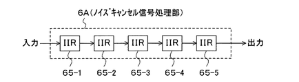
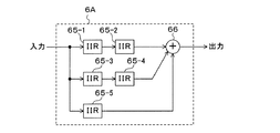
図7は、上記図6に示したノイズキャンセリングシステムにおいて、デシメーションフィルタ5A、デシメーションフィルタ5B、ノイズキャンセル信号処理部6A、DSP60内のノイズキャンセル信号処理部6、インターポレーションフィルタ7、及び合成器12から成る部位を抜き出して示したものとされる。この図により、上記2つの機能態様例のうちの1つである、第1の機能態様例について説明する。
7 shows a
先ず、第1の機能態様例としては、図7に示されるようにして、ノイズキャンセル用オーディオ信号を形成するノイズキャンセル信号処理部について、図4の構成に対応する第1のノイズキャンセル信号処理系に属するノイズキャンセル信号処理部6のほうをメイン処理部として扱うこととし、一方の第2のノイズキャンセル信号処理系に属するノイズキャンセル信号処理部6Aをサブ処理部として扱うようにされる。つまり、図5(d)に対応する構成である。
そして、この場合においてメイン処理部となるノイズキャンセル信号処理部6のデジタルフィルタについては、先にも述べたように、ノイズキャンセル対象となる全ての音声周波数帯域のうちで、有効なノイズキャンセル効果が得られるとされる一定以下の周波数帯域範囲に対応するノイズキャンセル信号処理を実行させるように構成する。つまり、ノイズキャンセル信号処理部6を備える第1のノイズキャンセル信号処理系は、デシメーションフィルタ5Bとインターポレーションフィルタ7を備えることで信号遅延を有するために、一定以上の高域について有効なノイズキャンセル効果を期待することが難しいが、ここでは、この一定以上の高域は除外して、これより低い中低域としての周波数帯域範囲を対象とするノイズキャンセル用オーディオ信号を生成するものである。
そのうえで、サブ処理部となるノイズキャンセル信号処理部6Aのデジタルフィルタについては、上記の高域を対象としてノイズキャンセルが行われるようにされた特性のノイズキャンセル用オーディオ信号を生成するように形成する。
そして、これらのメイン処理部とサブ処理部のノイズキャンセル用オーディオ信号が合成器12により合成される結果、合成器12から出力される総合のノイズキャンセル用オーディオ信号としては、ノイズキャンセル対象として必要とされる全音声周波数帯域にわたって有効なノイズキャンセル効果を生じる機能が与えられるものである。
このようにして、第1の機能態様例としては、先にも述べたように、先ず、第1のノイズキャンセル信号処理系により、中低域を対象とするノイズキャンセルを行うようにしたうえで、この第1のノイズキャンセル信号処理系では充分なノイズキャンセル効果を得にくい高域について、より信号遅延の少ない第2のノイズキャンセル信号処理系により補助的にキャンセルを行うように構成している。つまり、キャンセル対象とするノイズの周波数帯域を、第1、第2のノイズキャンセル信号処理系(ノイズキャンセル信号処理部6A、6)とで分担する。
この場合のノイズキャンセル信号処理部6Aは、先に図5(d)においても述べたように、単純なゲイン調整回路であるとか、数タップのFIRフィルタなどによる移動平均値を求める回路などの簡易なハードウェア構成により実現できるものであり、大幅なリソースの削減、回路規模の縮小などが図られる。また、DSP60内のノイズキャンセル信号処理部6についても、この場合には、高域について有効にノイズキャンセルを図るべきことを意図して構成する必要がないことから、その分、リソースは削減され、処理能力の点でも有利となる。また、このようにして、これまでより簡易な構成となることで、これらのノイズキャンセル信号処理部6、6Aとしてのフィルタの設計に関しても容易化が期待される。
First, as a first functional mode example, as shown in FIG. 7, a noise cancellation signal processing unit for forming a noise canceling audio signal as shown in FIG. The noise cancellation
In this case, as described above, the digital filter of the noise cancellation
In addition, the digital filter of the noise canceling
Then, as a result of the noise canceling audio signals of the main processing unit and the sub processing unit being combined by the
In this way, as described above, as the first functional mode example, first, after the first noise cancellation signal processing system performs noise cancellation for the middle and low range. In the first noise canceling signal processing system, the high frequency range where it is difficult to obtain a sufficient noise canceling effect is configured to be supplementarily canceled by the second noise canceling signal processing system with less signal delay. That is, the frequency band of noise to be canceled is shared by the first and second noise cancellation signal processing systems (noise cancellation
The noise cancellation
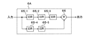
次に、図8を参照して、第2の機能態様例について説明する。なお、この図において、図7と同一部分には同一符号を付して説明を省略する。
第2の機能態様例としては、上記図7により説明した第1の機能態様例とは反対に、第2のノイズキャンセル信号処理系をメインの信号処理系とし、第1のノイズキャンセル信号処理系をサブの信号処理系とする。これに応じて、第2のノイズキャンセル信号処理系に属するノイズキャンセル信号処理部6Aがメイン処理部となり、第1のノイズキャンセル信号処理系に属するノイズキャンセル信号処理部6がサブ処理部となる。つまり、図5(c)に対応する構成である。
そして、その役割分担としては、図5(c)においても述べたように、メインとなるノイズキャンセル信号処理部6Aについては、ノイズキャンセル対象となる全ての音声周波数帯域における中高域を対象としてノイズキャンセルを行うためのノイズキャンセル信号を生成するようにして構成し、サブとなるノイズキャンセル信号処理部6については、ノイズキャンセル対象となる全ての音声周波数帯域における低域を対象としてノイズキャンセルを行うためのノイズキャンセル信号を生成するようにして構成するものである。
そして、この場合にも、合成器12により、メイン処理部とサブ処理部のノイズキャンセル用オーディオ信号を合成して得られるノイズキャンセル用オーディオ信号としては、ノイズキャンセル対象として必要とされる全音声周波数帯域にわたって有効なノイズキャンセル効果を生じる機能が与えられることになる。
Next, a second functional mode example will be described with reference to FIG. In this figure, the same parts as those in FIG.
As a second functional mode example, contrary to the first functional mode example described with reference to FIG. 7, the second noise cancellation signal processing system is the main signal processing system, and the first noise cancellation signal processing system is used. Is a sub signal processing system. Accordingly, the noise cancellation
As for the division of roles, as described in FIG. 5C, the noise cancellation
Also in this case, the noise canceling audio signal obtained by synthesizing the noise canceling audio signals of the main processing unit and the sub processing unit by the
なお、本実施の形態に基づくノイズキャンセリングシステムを実際に構成するのにあたって、上記第1の機能態様例と第2の機能態様例の何れを採用するのかについては、そのノイズキャンセリングシステムに要求されるコスト、仕様などの各種条件に応じて適当なほうを選べばよい。先の図5(c)(d)の説明からも理解されるように、低コストであることや、回路規模をできるだけ小さなものとすることを優先したい場合には、第1の機能態様例を採用することの方が有利となる。一方で、ハードウェアによるノイズキャンセル信号処理部6Aがメインの信号処理を実行するようにされた第2の機能態様例では、より高品位なノイズキャンセル効果を期待できる。従って、高品位な再生音を提供することを優先するような場合には、第2の機能態様例を採用することが妥当となる。
Note that, in actually configuring the noise canceling system based on the present embodiment, it is required for the noise canceling system as to which of the first functional aspect example and the second functional aspect example is adopted. Appropriate one may be selected according to various conditions such as cost and specifications. As can be understood from the description of FIGS. 5C and 5D, the first functional mode example is used when priority is given to low cost and to make the circuit scale as small as possible. Adopting is more advantageous. On the other hand, in the second functional mode example in which the noise cancellation
またここで、本実施の形態のノイズキャンセリングシステムのデジタルブロック800において、ノイズキャンセルのための信号処理系に関わる所定の機能回路部において採用するデジタルフィルタの構成について述べる。
例えば先に図4に示したノイズキャンセリングシステムにあっては、上記のデシメーションフィルタ5(5A、5B)、及びインターポレーションフィルタ7について、直線位相型FIRにより構成している。これは、先にも説明したように、処理対象がオーディオ信号とされているのであるから、一般的には、周波数に応じた位相歪みなどを生じさせないことが必要であるとの考え方に基づくものである。
直線位相型FIRとされることで、入出力間には群遅延が生じるが、これまでのA/Dコンバータ、D/Aコンバータのデバイスは、ユーザが積極的に聴こうとするオーディオ音源の再生(記録)に使用することを前提としていたために、特に問題になることはなかったものである。例えばオーディオ音源を再生する場合であれば、そのオーディオ音源の信号が信号処理デバイスに入力されてから音として再生するまでに、信号処理による相応の遅延が生じたとしても、ユーザが聴く音としては、正常に連続して再生出力されているものに他ならないわけであり、従って、ユーザがオーディオ音源を再生して聴くのに、信号処理の遅延が問題視されることはないからである。
しかしながら、オーディオ音源の再生ではなく、ノイズキャンセリングシステムにこれまでのデバイスを流用しようとすると、そのデバイスが持つ群遅延により、外部音を打ち消すことのできる位相を得ることができない、あるいは困難になってくるものであり、これが問題点として浮上してしまう。
Here, the configuration of a digital filter employed in a predetermined functional circuit unit related to a signal processing system for noise cancellation in the
For example, in the noise canceling system previously shown in FIG. 4, the decimation filter 5 (5A, 5B) and the
By adopting a linear phase FIR, a group delay occurs between input and output. However, conventional A / D converters and D / A converter devices reproduce audio sound sources that users actively listen to. Since it was assumed to be used for (recording), there was no particular problem. For example, in the case of playing an audio source, even if a corresponding delay occurs due to signal processing after the signal of the audio source is input to the signal processing device and played as a sound, This is because nothing is normally reproduced and output continuously. Therefore, when the user reproduces and listens to the audio sound source, the delay of signal processing is not regarded as a problem.
However, when trying to divert a conventional device to a noise canceling system instead of playing an audio source, it is impossible or difficult to obtain a phase that can cancel external sound due to the group delay of the device. This will come up as a problem.
図6に示す実施の形態のノイズキャンセリングシステムとしては、この問題点を、先ず、デシメーションフィルタ5B及びインターポレーションフィルタ7を経由しない、ノイズキャンセル信号処理部6Aを含む第2のノイズキャンセル信号処理系を設けることにより、解決しているものである。
しかし、そのうえでさらに、第1のノイズキャンセル信号処理系側についても、デシメーションフィルタ5(5A、5B)と、インターポレーションフィルタ7において顕著とされる信号遅延が短縮されるのであれば、ノイズキャンセル効果の阻害要因はそれだけ少なくなって、より良好な効果を期待できることになる。
In the noise canceling system of the embodiment shown in FIG. 6, this problem is first solved by the second noise cancellation signal processing including the noise cancellation
However, if the signal delay that is noticeable in the decimation filter 5 (5A, 5B) and the
そこで本実施の形態としては、先ず、1つの例として、図6に示されるデシメーションフィルタ5Bと、インターポレーションフィルタ7におけるアンチイメージングフィルタ7bとしてのデジタルフィルタについて、最小位相推移型FIRとした構成を採るようにされる。
なお、最小位相推移型FIRのデジタルフィルタの基本としては、FIR型のデジタルフィルタのシステムとして最小位相が得られるようにして、タップ係数について、先頭側(入力に近い側)にピークの値を設定することで形成できる。
Therefore, in the present embodiment, as an example, a configuration in which the
Note that the minimum phase transition FIR digital filter is based on the fact that the minimum phase can be obtained as the FIR digital filter system, and the peak value is set on the top side (side closer to the input) for the tap coefficient. Can be formed.
例えば、同じタップ数により構成した直線位相型FIRのデジタルフィルタと、最小位相推移型FIRのデジタルフィルタの特性として、インパルス応答波形について比較してみると、先ず、直線位相型FIRでは入力タイミングに対して或る一定時間遅延したタイミングで、そのピークが得られる。これは、入力に応答した出力としては、タップ数(次数)に応じた一定時間による遅延(群遅延)を持つということを示している。これに対して、最小位相推移型FIRでは、入力タイミングに対して、例えば数タップ分程度に相当する速いタイミングでピークが得られる。つまり、同じFIRデジタルフィルタでありながら、最小位相推移型FIRは、直線位相型FIRと比較して、入力に応答した出力の遅延(入出力遅延)の時間が非常に短い。
従って、デシメーションフィルタ5Bと、インターポレーションフィルタ7におけるアンチイメージングフィルタ7bとについて、最小位相推移型FIRを採用することとすれば、ここでの信号遅延時間は大幅に短縮されることとなり、信号遅延の要因がほぼ排除されることになる。これにより、第1のノイズキャンセル信号処理系としては、より良好なノイズキャンセル能力の得られることが期待される。
For example, when comparing impulse response waveforms as the characteristics of a digital filter of linear phase type FIR configured with the same number of taps and a digital filter of minimum phase shift type FIR, first, in the linear phase type FIR, The peak is obtained at a timing delayed for a certain time. This indicates that the output in response to the input has a delay (group delay) by a fixed time corresponding to the number of taps (order). On the other hand, in the minimum phase transition type FIR, a peak is obtained at a fast timing corresponding to, for example, about several taps with respect to the input timing. That is, although the same FIR digital filter is used, the minimum phase transition type FIR has a very short output delay (input / output delay) in response to the input as compared with the linear phase type FIR.
Therefore, if the minimum phase transition type FIR is adopted for the
なお、周知のようにして、最小位相推移型FIRの場合には、周波数に応じた位相歪みが生じる。従って、オーディオ信号の場合、この位相歪みによる音質劣化を生じる可能性は避けられないことになる。このことが、これまでにおいて、オーディオ信号対応のA/DコンバータやD/Aコンバータに実装するデジタルフィルタについて直線位相型FIRとしていたことの理由である。
しかしながら、この場合の信号処理対象は、オーディオ信号ではあるものの、例えばノイズキャンセル対象となる外部音であり、オーディオソースなどと比較すれば、要求される再生忠実度は相当に低い。そのうえでさらに、実際にあってキャンセル効果の大きいとされる音成分は、いわゆる低域といわれる低い周波数帯域であり、デバイスの特性などとの兼ね合いもあって、数kHz程度までのノイズキャンセルが有効にはたらけば、実使用上は充分であるとされている。このような見地からすると、例えば上記のデシメーションフィルタ5B、及びアンチイメージングフィルタ7bを最小位相推移型FIRにより形成したとしても、音質的な不具合などはほとんど生じない。
As is well known, in the case of the minimum phase transition type FIR, phase distortion corresponding to the frequency occurs. Therefore, in the case of an audio signal, the possibility of sound quality degradation due to this phase distortion is unavoidable. This is the reason why the A / D converter corresponding to the audio signal and the digital filter mounted on the D / A converter have been linear phase type FIRs so far.
However, although the signal processing target in this case is an audio signal, for example, it is an external sound that is a noise cancellation target, and the required reproduction fidelity is considerably low compared to an audio source or the like. In addition, the sound component that is actually considered to have a large cancellation effect is a low frequency band called a so-called low band, and noise cancellation up to several kilohertz is effective in consideration of device characteristics. If it works, it is said to be sufficient for practical use. From this point of view, even if the
また、上記の説明によると、デシメーションフィルタ5とインターポレーションフィルタ7の構成部位において、デシメーションフィルタ5Aとオーバーサンプリング回路7aについては最小位相推移型FIRとしていない。つまり、これらの部位については、直線位相型FIRとしている。
これは、デシメーションフィルタ5とインターポレーションフィルタ7における信号遅延の要因が、それぞれデシメーションフィルタ5Bとアンチイメージングフィルタ7bにおいて支配的であることによる。従って、デシメーションフィルタ5Aとオーバーサンプリング回路7aについて、例えば再生音質などを重視して直線位相型FIRを用いたとしても、ノイズキャンセル信号処理部6を経由する信号処理系での信号遅延は特に問題にはならないものである。
Further, according to the above description, the
This is because signal delay factors in the
また、上記のようにして、入出力間での信号遅延の短縮を目的とするのであれば、デシメーションフィルタ5Bとアンチイメージングフィルタ7bとについて、IIR(Infinite Impulse Response)フィルタにより構成することも妥当なものとなる。IIRフィルタのインパルス応答波形も、入力タイミングに対して、例えば数タップ分程度に相当する速いタイミングでピークが得られる特性を示す、即ち、入出力遅延は非常に短いものであり、最小位相推移型FIRにより構成した場合と同様にして、第1のノイズキャンセル信号処理系についての信号遅延をこれまでより少ないものとすることができる。
If the purpose is to reduce the signal delay between input and output as described above, it is also appropriate to configure the
また、第1のノイズキャンセル信号処理系におけるDSP60内のノイズキャンセル信号処理部6としてのデジタルフィルタについては、直線位相型FIRフィルタ、若しくはIIRフィルタにより形成することができる。なお、このノイズキャンセル信号処理部6としての直線位相型FIRフィルタ若しくはIIRフィルタは、例えばプログラミング(インストラクション)に従ってDSP60が動作を実行することで実現される機能回路である。
なお、ノイズキャンセル信号処理部6のほうがメイン処理部となる第1の機能態様例にあっては、プログラミングにより実現されるDSP60内の信号処理機能であっても、リソースの削減が図られるなどの点を考慮すれば、ノイズキャンセル信号処理部6をIIRフィルタにより構成することのほうが好ましい。
The digital filter as the noise cancellation
In the first functional mode example in which the noise cancellation
また、もう一方の第2のノイズキャンセル信号処理系に属するとされる、ノイズキャンセル信号処理部6Aとしてのデジタルフィルタについては、ノイズキャンセル信号を生成するための専用のハードウェアとして実装するものとされる。そのうえで、このノイズキャンセル信号処理部6Aについては、直線位相型FIR、若しくはIIRフィルタにより構成するようにされる。
ただし、現状において、第2の機能態様例に従って、第2のノイズキャンセル信号処理系(ノイズキャンセル信号処理部6A)をメインとし、第1のノイズキャンセル信号処理系(ノイズキャンセル信号処理部6)をサブとする構成を考えた場合には、先に図5(c)にても述べたように、ノイズキャンセル信号処理部6AをIIRフィルタにより構成することの方が、必要なリソース量を抑えながら高品位なノイズキャンセル効果を得ようという目的からは有利となる。
The digital filter as the noise cancellation
However, at present, according to the second functional mode example, the second noise cancellation signal processing system (noise cancellation
そのうえで、第2の機能態様例を採ることとした場合においては、さらに、ハードウェアとして構成されるノイズキャンセル信号処理部6Aについても、或る程度の自由度の範囲内において、その特性について可変設定できるようにすれば、例えばDSP60側のノイズキャンセル信号処理部6によってのみ特性を可変設定するようにした場合よりも高い適応性のノイズキャンセル信号処理が行えることとなって好ましいといえる。
そこで、ノイズキャンセル信号処理部6AについてIIRフィルタを採用する場合としては、例えば次のようにしてフィルタ特性を可変できるようにした構成を考えることができる。
In addition, when the second functional mode example is adopted, the noise cancellation
Therefore, as a case where an IIR filter is employed for the noise cancellation
先ずは、ノイズキャンセル信号処理部6Aを形成するデジタルフィルタとして、二次のIIRフィルタを複数備えることとする。ここでは、実際の演算ステップ数などを考慮して、二次のIIRフィルタとして、IIRフィルタ65−1、65−2、65−3、65−4、65−5の5つを用意する。そのうえで、ノイズキャンセル信号処理部6Aに必要とされる特性に応じて、これらのIIRフィルタ65−1〜65−5の接続態様のパターンを、図9〜図15に示すもののうちから適宜選択するようにされる。
図9には、IIRフィルタ65−1、65−2、65−3、65−4、65−5を直列に接続したパターンを示している。この場合には、直列接続の初段のIIRフィルタ65−1から信号を入力し、最終段のIIRフィルタ65−5から信号を出力する。
図10には、4つのIIRフィルタ65−1、65−2、65−3、65−4を直列接続した系と、残る1つのIIRフィルタ65−5のみの系を並列的に設けたパターンが示されている。入力信号は、各系に分岐して入力し、各系の出力は、合成器66により合成したうえでノイズキャンセル信号処理部6Aから出力させる。
図11には、3つのIIRフィルタ65−1、65−2、65−3を直列接続した系と、残る2つのIIRフィルタ65−4、65−5を直列接続した系とを並列的に設けたパターンが示されている。入力信号は、各系に分岐して入力し、各系の出力は、合成器66により合成したうえでノイズキャンセル信号処理部6Aから出力させる。
図12には、3つのIIRフィルタ65−1、65−2、65−3を直列接続した系と、IIRフィルタ65−4のみから成る系と、IIRフィルタ65−5のみから成る系とを、それぞれ並列に接続したパターンが示される。入力信号は、これら3つの系に分岐して入力され、各系の出力は、合成器66により合成したうえでノイズキャンセル信号処理部6Aから出力させる。
図13には、2つのIIRフィルタ65−1、65−2を直列接続した系と、2つのIIRフィルタ65−3、65−4を直列接続した系と、1つのIIRフィルタ65−5のみから成る系とを並列的に設けたパターンが示されている。入力信号は、各系に分岐して入力し、各系の出力は、合成器66により合成したうえでノイズキャンセル信号処理部6Aから出力させる。
図14には、2つのIIRフィルタ65−1、65−2を直列接続した系と、IIRフィルタ65−3のみによる系と、IIRフィルタ65−4のみによる系と、IIRフィルタ65−5のみによる系とを並列的に設けたパターンが示されている。入力信号は、各系に分岐して入力し、各系の出力は、合成器66により合成したうえでノイズキャンセル信号処理部6Aから出力させる。
図15は、5つのIIRフィルタ65−1、IIRフィルタ65−2、IIRフィルタ65−3、IIRフィルタ65−4、及びIIRフィルタ65−5を並列的に設けたパターンが示されている。入力信号は、各フィルタに分岐して入力し、各フィルタの出力は、合成器66により合成したうえでノイズキャンセル信号処理部6Aから出力させる。
なお、上記図9〜図15に示したような構成は、例えばシーケンサなどの手法を用いて1つのハードウェア資源(リソース)を時間軸に従って再使用することで、より少ないハードウェア資源で実現できるものである。
First, a plurality of secondary IIR filters are provided as digital filters forming the noise cancellation
FIG. 9 shows a pattern in which IIR filters 65-1, 65-2, 65-3, 65-4, and 65-5 are connected in series. In this case, a signal is input from the first-stage IIR filter 65-1 connected in series, and a signal is output from the final-stage IIR filter 65-5.
FIG. 10 shows a pattern in which a system in which four IIR filters 65-1, 65-2, 65-3, 65-4 are connected in series and a system in which only the remaining one IIR filter 65-5 is provided in parallel. It is shown. The input signal is branched and input to each system, and the output of each system is synthesized by the
FIG. 11 shows in parallel a system in which three IIR filters 65-1, 65-2, 65-3 are connected in series and a system in which the remaining two IIR filters 65-4, 65-5 are connected in series. The provided pattern is shown. The input signal is branched and input to each system, and the output of each system is synthesized by the
FIG. 12 shows a system in which three IIR filters 65-1, 65-2, and 65-3 are connected in series, a system that includes only the IIR filter 65-4, and a system that includes only the IIR filter 65-5. Each pattern connected in parallel is shown. The input signal is branched and input to these three systems, and the output of each system is synthesized by the
FIG. 13 shows a system in which two IIR filters 65-1 and 65-2 are connected in series, a system in which two IIR filters 65-3 and 65-4 are connected in series, and only one IIR filter 65-5. A pattern in which a system consisting of the above is provided in parallel is shown. The input signal is branched and input to each system, and the output of each system is synthesized by the
In FIG. 14, a system in which two IIR filters 65-1 and 65-2 are connected in series, a system by only IIR filter 65-3, a system by only IIR filter 65-4, and only by IIR filter 65-5. A pattern in which the system is provided in parallel is shown. The input signal is branched and input to each system, and the output of each system is synthesized by the
FIG. 15 shows a pattern in which five IIR filters 65-1, IIR filter 65-2, IIR filter 65-3, IIR filter 65-4, and IIR filter 65-5 are provided in parallel. The input signal is branched and input to each filter, and the output of each filter is synthesized by the
The configurations shown in FIGS. 9 to 15 can be realized with fewer hardware resources by reusing one hardware resource (resource) according to the time axis by using a method such as a sequencer. Is.
また、先に、第1の機能態様例を採ることとした場合には、DSP60内のノイズキャンセル信号処理部6についてはIIRフィルタにより構成することが好ましいと述べたが、このようにしてノイズキャンセル信号処理部6をIIRフィルタとして構成しようとする場合には、DSP60に対するプログラミングにより、上記図9〜図15により説明した構成を採用することができるものである。
In addition, when the first functional mode example is adopted, it has been described that the noise cancellation
そこで、本実施の形態のノイズキャンセリングシステムとして第1の機能態様例を採用したうえで、DSP60内のノイズキャンセル信号処理部6として、図9に示したパターンを採用した場合における、IIRフィルタ65−1〜65−5ごとの特性の設定例を、図16に示すこととする。
この場合、先ず、初段のIIRフィルタ65−1は、入力信号にゲインを与えて出力するゲイン設定回路としての機能を与えるようにされる。ここでは、そのゲイン係数 (Gain)として0.035を設定するようにされる。
また、続く2段目から5段目(最終段)までの各IIRフィルタ65−2〜65−5については、いわゆるパラメトリックイコライザといわれる機能が与えられるようにされる。そして、イコライザ特性として、IIRフィルタ65−2については、中心周波数fc=20Hz、Q値=0.4、ゲイン値G=28dBを設定し、IIRフィルタ65−3については、中心周波数fc=800Hz、Q値=0.6、ゲイン値G=12dBを設定し、IIRフィルタ65−4については、中心周波数fc=10000Hz、Q値=3.2、ゲイン値G=−21dBを設定し、IIRフィルタ65−5については、中心周波数fc=18500Hz、Q値=2.5、ゲイン値G=−16dBを設定するようにされる。
また、ここでは図示していないが、上記のノイズキャンセル信号処理部6の構成に対応させて、ノイズキャンセル信号処理部6Aはゲイン調整回路として構成するようにされる。そして、そのゲイン係数については、例えば0.012を設定する。
Therefore, the first functional example is adopted as the noise canceling system of the present embodiment, and the IIR filter 65 in the case where the pattern shown in FIG. 9 is adopted as the noise cancellation
In this case, first, the IIR filter 65-1 in the first stage is given a function as a gain setting circuit that gives a gain to an input signal and outputs the gain. Here, 0.035 is set as the gain coefficient (Gain).
The IIR filters 65-2 to 65-5 from the second stage to the fifth stage (final stage) are provided with a function called a so-called parametric equalizer. As the equalizer characteristics, the center frequency fc = 20 Hz, the Q value = 0.4, and the gain value G = 28 dB are set for the IIR filter 65-2, and the center frequency fc = 800 Hz for the IIR filter 65-3. The Q value = 0.6 and the gain value G = 12 dB are set. For the IIR filter 65-4, the center frequency fc = 10000 Hz, the Q value = 3.2, the gain value G = -21 dB is set, and the IIR filter 65 is set. For −5, the center frequency fc = 18500 Hz, the Q value = 2.5, and the gain value G = −16 dB are set.
Although not shown here, the noise cancellation
ここで、図4に基づく構成(設計)によるノイズキャンセリングシステム(シングルパス構成のノイズキャンセリングシステム)と、図6に基づいて構成(設計)した本実施の形態のノイズキャンセリングシステム(デュアルパス構成のノイズキャンセリングシステム)とについての特性を比較した結果を、図21のボード線図に示す。ボード線図として図21(a)には、図4に基づくシングルパス構成によるノイズキャンセリングシステムの、周波数対ゲイン特性、周波数対位相特性が示され、図21(b)には、図6に基づくデュアルパス構成によるノイズキャンセリングシステムの、周波数対ゲイン特性、周波数対位相特性が示されている。また、図21(b)に示す特性を得るのにあたっては、図6におけるデシメーションフィルタ5B、アンチイメージングフィルタ7bとしてのデジタルフィルタについて最小位相推移型FIRを採用し、ノイズキャンセル信号処理部6AについてはIIRにより構成しているものとする。
例えばここでは、フィードフォワード方式によるノイズキャンセリングシステムに求めるべき目標の周波数対ゲイン特性としては、図21(a)(b)のそれぞれにおける周波数対ゲイン特性図において破線で示している特性であることを前提としている。なお、この破線で示す目標特性について、その周波数の上限を2kHzまでとしているのは、現実においてノイズキャンセルの制御対象となる音声の周波数帯域が2kHz程度までであることに依る。また、図21(b)に示される周波数対ゲイン特性では、100kHz付近まで一定以上のゲインが維持されているのに対して、図21(a)に示す周波数対ゲイン特性では、20kHz近傍にて急峻に減衰する特性となっている。これは、図4に基づく構成によるノイズキャンセリングシステムでは、サンプリング周波数が1fsのみの信号を対象としてノイズキャンセル処理を行うことから、サンプリング定理に基づくエリアシングを避けるために、fs/2で表されるサンプリング周波数よりも高い帯域を除去しているためである。ちなみに、この場合には、fs=44.1kHzとしており、従って図21(a)に示される周波数対ゲイン特性は、22.05kHzより高い周波数帯域を減衰させた結果が示されている。
Here, a noise canceling system (single-path configuration noise canceling system) based on the configuration (design) based on FIG. 4 and the noise canceling system (dual path configuration) of the present embodiment configured (designed) based on FIG. FIG. 21 is a Bode diagram showing the result of comparing the characteristics of the noise canceling system having the configuration. As a Bode diagram, FIG. 21 (a) shows frequency vs. gain characteristics and frequency vs. phase characteristics of a noise canceling system with a single path configuration based on FIG. 4, and FIG. 21 (b) shows FIG. The frequency vs. gain and frequency vs. phase characteristics of a noise canceling system with a dual path configuration based thereon are shown. In order to obtain the characteristics shown in FIG. 21B, the minimum phase transition FIR is adopted for the digital filter as the
For example, here, the target frequency-to-gain characteristic to be obtained for the feed-forward noise canceling system is the characteristic indicated by the broken line in each of the frequency-to-gain characteristic diagrams in FIGS. Is assumed. The reason why the upper limit of the frequency of the target characteristic indicated by the broken line is set to 2 kHz depends on the fact that the frequency band of the voice to be controlled for noise cancellation is actually about 2 kHz. Further, in the frequency vs. gain characteristic shown in FIG. 21 (b), a gain above a certain level is maintained up to around 100 kHz, whereas in the frequency vs. gain characteristic shown in FIG. 21 (a) , around 20 kHz. It has a characteristic of steep decay. This is expressed by fs / 2 in order to avoid aliasing based on the sampling theorem because the noise canceling system having the configuration based on FIG. 4 performs noise cancellation processing on a signal having a sampling frequency of only 1 fs. This is because a band higher than the sampling frequency is removed. Incidentally, in this case, fs = 44.1 kHz, and therefore the frequency vs. gain characteristic shown in FIG. 21 (a) shows the result of attenuating a frequency band higher than 22.05 kHz.
ここで、例えば図21(a)と図21(b)とを比較してみると、先ず、周波数対ゲイン特性については、現実にノイズキャンセル対象となる2KHz程度までの周波数帯域の範囲ではほぼ同等となっている。しかし、周波数対位相特性については、図21(b)のデュアルパス構成のほうでは、2kHz〜10kHz程度の範囲でほぼ0deg.に近い値が得られているのに対して、図21(a)のシングルパス構成について同じ2kHz〜10kHz程度の範囲をみてみると、絶対値として100deg.以上の位相回転を生じるようにしておおきく変動している。このようにして、本実施の形態に基づくノイズキャンセリングシステムとしては実際においても信号の位相回転が大幅に縮小されるという結果が得られているものであり、デジタルシステムでありながら、実用に足るノイズキャンセリングシステムを得ることも現実において容易に可能とされるものである。 Here, for example, comparing FIG. 21 (a) and FIG. 21 (b), first, the frequency-to-gain characteristics are substantially the same in the frequency band range up to about 2 KHz that is actually subject to noise cancellation. It has become. However, with respect to the frequency vs. phase characteristics, the dual path configuration in FIG. 21B has a value close to 0 deg. In the range of about 2 kHz to 10 kHz, whereas FIG. Looking at the same range of about 2 kHz to 10 kHz for the single path configuration, the absolute value fluctuates so as to cause a phase rotation of 100 degrees or more. In this way, the noise canceling system based on the present embodiment has obtained the result that the phase rotation of the signal is greatly reduced even in practice, and it is sufficient for practical use even though it is a digital system. Obtaining a noise canceling system is also easily possible in reality.
図17は、第2の実施の形態としてのノイズキャンセリングシステムの構成例を示している。なお、この図において、先の第1の実施の形態に対応する図6と同一とされる部分については、同一符号を付して説明を省略する。 FIG. 17 shows a configuration example of a noise canceling system as the second embodiment. In this figure, the same parts as those in FIG. 6 corresponding to the previous first embodiment are denoted by the same reference numerals and description thereof is omitted.
先に図1〜図3によっても説明したように、ヘッドフォン装置のノイズキャンセリングシステムには、大別して、フィードフォワード方式とフィードバック方式とが知られている。そして、これまでに述べてきた第1の実施の形態は、フィードフォワード方式に基づいた構成とされている。本願発明としては、フィードフォワード方式のみではなく、フィードバック方式にも適用できる。そこで、第2の実施の形態として、図1にそのモデルを示したフィードバック方式を基としたノイズキャンセリングシステムの構成例を示す。 As described above with reference to FIGS. 1 to 3, a noise canceling system for a headphone device is roughly classified into a feed forward method and a feedback method. And the 1st Embodiment described so far is set as the structure based on a feedforward system. The present invention can be applied not only to the feed forward method but also to the feedback method. Therefore, as a second embodiment, a configuration example of a noise canceling system based on a feedback system whose model is shown in FIG. 1 is shown.
フィードバック方式の場合には、図17において模式的に示すようにして、マイクロフォン2Bを、ヘッドフォンユニット1cの内部において、ドライバ1aから出力される音がヘッドフォン装着者の耳の近傍にて収音できるような位置に設けるようにされる。
この位置にてマイクロフォン2Bにより収音される音には、ドライバから出力される音とともに、例えばヘッドフォン装置の筐体にまで侵入してヘッドフォン装置者の耳に聴こえようとする外部音の成分も含まれている。このようにして収音された音の信号が、アンプ3Aにより増幅されてアナログ音声信号とされ、さらにLSI600のアナログブロック700のΔΣ変調器4Aに入力されて、ここで64fs、1ビットによるデジタルオーディオ信号に変換され、スイッチSW11を介して、デジタルブロック800のデシメーションフィルタ5−1のデシメーションフィルタ5Cに対して入力される。
なお、この場合においても、拡張性などを配慮して、マイクロフォン2Bと併行してデジタルマイク入力が備えられており、このデジタルマイク入力からのデジタルオーディオ信号と、ΔΣ変調器4Aから出力されるマイクロフォン2Bからのデジタルオーディオ信号とを、スイッチSW11により選択することが可能とされている。
In the case of the feedback method, as schematically shown in FIG. 17, the
The sound picked up by the
Even in this case, in consideration of expandability, a digital microphone input is provided in parallel with the
デシメーションフィルタ5−1は、フィードバック方式のノイズキャンセル信号処理の系において、A/D変換により得られた64fs、1ビットの信号をデジタルブロック800における信号処理に適合したサンプリング周波数にデシメーションするためのフィルタであり、図6との対応では、デシメーションフィルタ5に相当する。また、このデシメーションフィルタ5−1を形成するとされるデシメーションフィルタ5C、5Dは、図6との対応では、それぞれデシメーションフィルタ5A、5Bに相当する。デシメーションフィルタ5Cにより8fsにデシメーションされた信号は、分岐してノイズキャンセル信号処理部6Bに対しても入力され、デシメーションフィルタ5Dにより1fsにデシメーションされた信号は、DSP60におけるノイズキャンセル信号処理部6に対して入力されることになる。ノイズキャンセル信号処理部6Bは、フィードバック方式に対応して設けられたとする第2のノイズキャンセル信号処理系において設けられるものであり、図6との対応では、ノイズキャンセル信号処理部6Aが対応する。
The decimation filter 5-1 is a filter for decimating a 64 fs, 1-bit signal obtained by A / D conversion to a sampling frequency suitable for signal processing in the
この場合のノイズキャンセル信号処理部6、6Bは、例えば入力された信号について所要の特性を与えることで、ノイズキャンセル用オーディオ信号として、ヘッドフォン装着者のドライバ1a側の耳に到達して聴こえる外部音声をキャンセルすることのできる特性を有する音のオーディオ信号を生成する。これは、一般には収音音声の信号に対して、ノイズキャンセルのための伝達関数−βを与える処理となる。
なお、これらのノイズキャンセル信号処理部6、6Bについても、先に第1の実施の形態においても述べた、第1、第2の機能態様例の考え方、及び第1、第2の機能態様例に従った構成を適用できる。また、ノイズキャンセル信号処理部6、6Bとしてのデジタルフィルタについての形式、構成についても、第1の実施の形態と同様の形式、構成を適用できる。
In this case, the noise cancellation
For these noise cancellation
また、フィードバック方式に関しては、DSP60内のイコライザ61を、第1のノイズキャンセル信号処理系に含めて用いることが、良好なノイズキャンセル効果を得るために有効とされる。
この場合のイコライザ61は、1+βの伝達関数による特性を、デジタルオーディオソースの信号に与えるためのものとされる。フィードバック方式の場合、ノイズキャンセル信号処理部6から出力されるノイズキャンセル用オーディオ信号には、外部音に対応する成分だけではなく、ドライバ1aから音として出力されたデジタルオーディオソースの音を収音した成分も含まれている。つまり、デジタルオーディオソースの音成分に対して1/1+βで表される伝達関数に応じた特性が与えられる。そこで、このイコライザ61により、予めデジタルオーディオソースの信号に対して、1/1+βの逆数となる1+βの伝達関数による特性を与えておくようにされる。これにより、インターポレーションフィルタ14からのデジタルオーディオソースの信号が合成器12にてノイズキャンセル用オーディオ信号と合成された段階で、上記の1/1+βの伝達特性が打ち消されることになる。これにより、合成器12から出力される信号としては、外部音をキャンセルする特性を有する信号成分と、元のデジタルオーディオソースの信号成分とが合成されたものを得ることができる。
As for the feedback method, it is effective to use the
In this case, the
この場合の合成器12より後段の構成は、図6と同様となる。つまり、合成器12の出力としての信号は、ノイズシェイパ8、PWM回路9、及びパワードライブ回路10を介することで増幅された音声信号とされ、これがさらにフィルタ11、コンデンサC1を介してドライバ1aに供給されることで、ドライバ1aを駆動して音を出力させることになる。
このようにして、フィードバック方式では、ヘッドフォン装着者の耳の近傍にてドライバから出力される音とともに混入してきた外部音成分を収音してノイズキャンセル用の信号を生成する。そして、このノイズキャンセル用の信号を、負帰還をかけるようにしてドライバから出力させるものである。この結果、ヘッドフォン装置者のドライバ1aに対応する耳に対しては、外部音が打ち消され、デジタルオーディオソースの音が相対的に強調された音が到達して聴こえることになる。
そして、このようなフィードバック方式に対応するノイズキャンセリングシステムの構成においても、第1の実施の形態と同様にして、DSP60のノイズキャンセル信号処理部6を経由する第1のノイズキャンセル信号処理系に加えて、ノイズキャンセル信号処理部6Bを経由する第2のノイズキャンセル信号処理系を備えることで、第1の実施の形態と同様の効果を得ることが可能になるものである。
The configuration subsequent to the
In this manner, in the feedback method, the external sound component mixed with the sound output from the driver in the vicinity of the ear of the headphone wearer is collected to generate a signal for noise cancellation. The noise canceling signal is output from the driver with negative feedback applied. As a result, the external sound is canceled out to the ear corresponding to the
Even in the configuration of the noise canceling system corresponding to such a feedback system, the first noise cancellation signal processing system that passes through the noise cancellation
図18は、第3の実施の形態としてのノイズキャンセリングシステムの構成例を示している。なお、この図において、先の第1、第2の実施の形態に対応する図6、図17と同一とされる部分については、同一符号を付して説明を省略する。 FIG. 18 shows a configuration example of a noise canceling system according to the third embodiment. In this figure, parts that are the same as those in FIGS. 6 and 17 corresponding to the first and second embodiments are given the same reference numerals, and descriptions thereof are omitted.
この第3の実施の形態は、第1の実施の形態が対応するフィードフォワード方式と、第2の実施の形態が対応するフィードバック方式の系も併用することとした構成を採るものである。
先に若干述べたが、フィードバック方式とフィードフォワード方式とでは、相互にトレードオフとなるような関係の特徴を持っている。
例えば、フィードフォワード方式では、ノイズを有効にキャンセル(減衰)できる周波数帯域は広く、系の安定性も高いが、充分なノイズキャンセル量が得られにくいとされている。このために、例えばノイズ音源との位置関係などの状況によっては、系の伝達関数と合致しなくなり、例えば特定の周波数帯域にてノイズがキャンセルされない、あるいは増加してしまうような可能性のあることが指摘されている。この場合、実際には広い周波数帯域にわたってノイズキャンセルが有効にはたらいているのにも関わらず、或る特定の周波数帯域においてのみノイズが目立ってしまうような現象が生じるということになり、聴感上は、ノイズキャンセル効果を感じにくくなる。
これに対して、フィードバック方式は、ノイズをキャンセルできる周波数帯域は狭いものの、充分なノイズキャンセル量が得られるという特徴を持っている。
このことからすると、フィードフォワード方式に対してフィードバック方式を組み合わせてノイズキャンセリングシステムを構築すれば、相互の不利点を補い合うことで、広い周波数帯域全体にわたってノイズ音を有効にキャンセルすることが容易に可能となる。即ち、何れか一方の方式のみに基づく場合よりも良好なノイズキャンセル効果を期待できる。
The third embodiment adopts a configuration in which a feedforward system corresponding to the first embodiment and a feedback system corresponding to the second embodiment are used in combination.
As described above, the feedback method and the feedforward method have a characteristic of a relationship that is a trade-off between them.
For example, in the feedforward system, the frequency band in which noise can be effectively canceled (attenuated) is wide and the system is highly stable, but it is difficult to obtain a sufficient amount of noise cancellation. For this reason, depending on the situation such as the positional relationship with the noise source, for example, it may not match the transfer function of the system, and noise may not be canceled or increased in a specific frequency band, for example. Has been pointed out. In this case, although noise cancellation is actually effective over a wide frequency band, a phenomenon that noise becomes conspicuous only in a specific frequency band occurs. This makes it difficult to feel the noise cancellation effect.
On the other hand, the feedback system has a feature that a sufficient amount of noise cancellation can be obtained although the frequency band in which noise can be canceled is narrow.
From this, if a noise canceling system is constructed by combining a feedback method with a feedforward method, it is easy to effectively cancel noise noise over the entire wide frequency band by making up for each other's disadvantages. It becomes possible. In other words, a better noise cancellation effect can be expected than when only one of the methods is used.
そして、図18に示される第3の実施の形態としての構成においては、先ず、フィードフォワード方式の系に対応するものとして、図6と同様にして、マイクロフォン2F、アンプ3、ΔΣ変調器4、スイッチSW1、デシメーションフィルタ5(デシメーションフィルタ5A、5B)、及びノイズキャンセル信号処理部6Aが示される。また、フィードバック方式の系に対応するものとして、図17と同様にして、マイクロフォン2B、アンプ3A、ΔΣ変調器4A、スイッチSW11、デシメーションフィルタ5−1(デシメーションフィルタ5C、5D)、及びノイズキャンセル信号処理部6Bが示される。
In the configuration of the third embodiment shown in FIG. 18, first, as corresponding to the feedforward system, the
また、この場合のDSP60のノイズキャンセル信号処理部6は、フィードフォワード方式の系に対応するデシメーションフィルタ5Bからの信号と、フォードバック方式の系に対応するデシメーションフィルタ5Dからの信号とを入力して、ノイズキャンセル用オーディオ信号を生成して出力するものとして示されている。
実際において、この場合のノイズキャンセル信号処理部6においては、デシメーションフィルタ5Bからの信号を入力してフィードフォワード方式に対応するノイズキャンセル用オーディオ信号を生成するフィルタと、デシメーションフィルタ5Dからの信号を入力してフィードバック方式に対応するノイズキャンセル用オーディオ信号を生成するフィルタとを有するものとされる。そして、例えばノイズキャンセル信号処理部6のなかで、これらのフィルタにより生成されたノイズキャンセル用オーディオ信号を合成したうえで、インターポレーションフィルタ7に対して出力するような構成を採ることになる。
In this case, the noise canceling
Actually, in this case, the noise cancellation
そして、この場合の合成器12においては、ノイズキャンセル信号処理部6A、6B、及びインターポレーションフィルタ7からの各ノイズキャンセル用オーディオ信号と、インターポレーションフィルタ14からのデジタルオーディオソースの信号とを合成して後段の回路(ノイズシェイパ8)に出力するようにされる。
In the
このようにして、第3の実施の形態のノイズキャンセリングシステムは、図6に対応するフィードフォワード系としての第1、第2のノイズキャンセル信号処理系の構成と、図17に対応するフィードバック系としての第1、第2のノイズキャンセル信号処理系の構成とを組み合わせて構成される。この構成により、先にも述べたようにして、何れか一方の方式のみに基づく場合よりも良好なノイズキャンセル効果が得られることになるものである。 As described above, the noise canceling system according to the third embodiment includes the configurations of the first and second noise cancellation signal processing systems as the feedforward system corresponding to FIG. 6 and the feedback system corresponding to FIG. And the first and second noise cancellation signal processing systems. With this configuration, as described above, a better noise canceling effect can be obtained than in the case where only one of the methods is used.
図19は、第4の実施の形態としてのノイズキャンセリングシステムの構成例を示している。なお、この図に示されるノイズキャンセリングシステムは、フィードフォワード方式に対応したもので、構成部位としては、図6と同様となるものである。
図6に示した第1の実施の形態にあっては、デジタルブロック800は、1つのチップとして製造されるものであるとして説明した。しかしながら、デジタルブロック800内の機能回路部において入出力される信号のサンプリング周波数に着目してみると、これは一律ではなく、いくつかの種類のあることがわかる。このようにして機能回路部間で対応するサンプリング周波数が相違する場合、現実にLSIを製造する場合の条件などを考慮した場合には、デジタルブロック800に備えられる機能回路部について、対応するサンプリング周波数に基づいてグループ分けし、これらのグループ分けされた機能回路部ごとにまとめてチップ化するようにして製造することのほうが効率的な場合もあると考えられる。
そこで、本実施の形態としては、デジタルブロック800を形成するチップとして、次のようにして構成することとする。
まず、図19に示されるデジタルブロック800において扱う信号のサンプリング周波数のうちでメインとなるものを考えてみた場合、1つは第1のノイズキャンセル信号処理系に対応するDSP60を主体とした1fsであり、もう1つは、第2のノイズキャンセル信号処理系に対応した8fsであるとみることができる。
FIG. 19 shows a configuration example of a noise canceling system as the fourth embodiment. Note that the noise canceling system shown in this figure corresponds to the feed-forward system, and the constituent parts are the same as those in FIG.
In the first embodiment shown in FIG. 6, the
Therefore, in this embodiment, the chip that forms the
First, considering the main sampling frequency of signals handled in the
そこで、本実施の形態としては、図示するようにして、先ず、1fsに対応するDSP60としての回路部位を少なくとも形成した1つのチップとして第1信号処理チップ810を製造するとともに、これとは別に、8fsに対応する機能回路部として、デシメーションフィルタ5(5A、5B)、ノイズキャンセル信号処理部6A、インターポレーションフィルタ7、インターポレーションフィルタ14、及び合成器12としての各回路部位を少なくとも形成した1つのチップとして第2信号処理チップ820を製造するようにされる。
Therefore, as shown in the present embodiment, as shown in the figure, first, the first
なお、図において第1信号処理チップ810と第2信号処理チップ820の何れにも含まれていない中のデジタルブロック800内の機能回路部については、適宜、第1信号処理チップ810と第2信号処理チップ820のうちの適当とされる側に含めることとする、あるいは、第1信号処理チップ810、及び第2信号処理チップ820以外の他のチップも製造することとして、これらのチップに含めるようにしてもよい。
It should be noted that in the figure, the functional circuit portion in the
なお、この図19に示される第4の実施の形態としての構成は、第2の実施の形態として図17に示したフィードバック方式に対応するノイズキャンセリングシステムのデジタルブロック800に対しても同様にして適用可能である。
つまり、1fsに対応するDSP60としての回路部位を少なくとも形成した第1信号処理チップ810と、8fsに対応する機能回路部として、デシメーションフィルタ5−1(5C、5D)、ノイズキャンセル信号処理部6B、インターポレーションフィルタ7、インターポレーションフィルタ14、及び合成器12としての各回路部位を少なくとも形成した第2信号処理チップ820を製造するものである。
The configuration of the fourth embodiment shown in FIG. 19 is the same as that of the
That is, the first
さらに第4の実施の形態としての構成は、第3の実施の形態として図18に示したフィードフォワード方式とフィードバック方式とを併用したノイズキャンセリングシステムのデジタルブロック800についても適用できる。この構成を、第5の実施の形態として図20に示す。
図20には、1fsに対応するDSP60としての回路部位を少なくとも形成した第1信号処理チップ810と、8fsに対応する機能回路部として、デシメーションフィルタ5、5−1(5A、5B、5C、5D)、ノイズキャンセル信号処理部6A、6B、インターポレーションフィルタ7、インターポレーションフィルタ14、及び合成器12としての各回路部位を少なくとも形成した第2信号処理チップ820が示される。
Furthermore, the configuration of the fourth embodiment can be applied to the
In FIG. 20, decimation filters 5, 5-1 (5A, 5B, 5C, 5D) are provided as a first
なお、これまでの実施の形態において述べてきた、LSI600内の機能回路部において入出力される信号のサンプリング周波数、及び量子化ビット数は、あくまでも代表的なものの1つであり、ノイズキャンセリングシステムの系の形成に破綻を生じない範囲で、必要に応じて、各機能回路部が扱うべきサンプリング周波数、及び量子化ビット数については変更されてよいものである。
Note that the sampling frequency and the number of quantization bits of signals input / output in the functional circuit section in the
また、これまでの実施の形態においては、第1のノイズキャンセル信号処理系と、第2のノイズキャンセル信号処理系との2系統が示されているデュアルパスとしての態様を示しているが、これを発展させて、例えば、第2のノイズキャンセル信号処理系をさらに複数系列設けるようにした構成も本願発明の下では考えられるものである。このような構成では、第2のノイズキャンセル信号処理系の複数系列ごとに、例えば異なるサンプリング周波数の信号を入力してノイズキャンセル用オーディオ信号を生成するようにして、各系の役割を分担させることが考えられる。なお、このようにして、第2のノイズキャンセル信号処理系を2系列以上設けた構成については「マルチパス」ともいうことにする。
ここで、上記のようにして第2のノイズキャンセル信号処理系を2系列以上設けるマルチパス構成とする場合において、このマルチパス構成の基となる信号処理系のモデル例を図22に示しておくこととする。
図22では、モデル例として、サンプリング周波数=64fsの信号をマルチパス化し、最終的に同じ64fsの形式により合成出力する構成を示している。
この図においては、先ず、ダウンサンプリング回路91−1〜91−6、信号処理ブロック92−0〜92−6、アップサンプリング回路94−1〜94−6、及び合成器93−0〜93−5を備える。
ダウンサンプリング回路91−1〜91−6は、それぞれ、入力信号のサンプリング周波数を1/2にダウンサンプリングして出力する。そして、これらダウンサンプリング回路91−1〜91−6は、直列に接続されたうえで、初段のダウンサンプリング回路91−1に対してサンプリング周波数=64fsの入力信号を入力させることとしている。これによりダウンサンプリング回路91−1〜91−6からは、それぞれ、入力信号のサンプリング周波数を、32fs、16fs、8fs、4fs、2fs、1fsに変換した信号が出力される。なお、サンプリング周波数が32fs以下の信号の量子化ビット数については、所定ビット数によるマルチビットとなるようにされる。
信号処理ブロック92−0〜92−6は、入力信号について所定目的に応じた信号処理を実行するための部位とされ、例えば所定の信号特性が与えられたデジタルフィルタなどとされる。この信号処理ブロックが、マルチパス化されたときの各パスにおけるノイズキャンセル信号処理部6Aに相当することになる。
これらの信号処理ブロック92−0〜92−6には、それぞれ、サンプリング周波数=64fsの入力信号、ダウンサンプリング回路91−1〜91−6から出力される、サンプリング周波数=32fs、16fs、8fs、4fs、2fs、1fsの信号が入力される。信号処理ブロック92−0〜92−6は、これらの信号をそれぞれ入力して、入力と同じサンプリング周波数(及び量子化ビット数)により出力する。
アップサンプリング回路94−1〜94−6は、入力される信号についてサンプリング周波数を2倍にアップサンプリングして出力する。アップサンプリング回路94−1〜94−5には、次に説明する合成器93−1〜93−5からの32fs、16fs、8fs、4fs、2fsの信号が入力されるようになっている。アップサンプリング回路94−6については、信号処理ブロック92−6からの1fsの信号が入力されるようになっている。
合成器93−0〜93−5は、それぞれ、信号処理フィルタ92−0〜92−5から出力される64fs、32fs、16fs、8fs、4fs、2fsの信号を入力するとともに、アップサンプリング回路94−1〜94−6から出力される64fs、32fs、16fs、8fs、4fs、2fsの信号を入力し、これらを合成するようにされる。合成器93−1〜93−5の各出力は、アップサンプリング回路94−1から94−5に対して入力されるようになっている。合成器93−0の出力が、最終的な64fsによる出力信号となる。
そして、実際に第2のノイズキャンセル信号処理系についてマルチパス化を行うのにあたっては、上記図22に示した構成を基にして、必要とされるサンプリング周波数による系が得られるようにして、必要なダウンサンプリング回路、アップサンプリング回路、合成器を構成したうえで、各系において、しかるべき信号処理が実行されるように信号処理ブロック(ノイズキャンセル信号処理部)を構成するようにされる。
Further, in the embodiments so far, a dual path mode is shown in which two systems of the first noise cancellation signal processing system and the second noise cancellation signal processing system are shown. For example, a configuration in which a plurality of second noise cancellation signal processing systems are further provided is also conceivable under the present invention. In such a configuration, for example, a signal having a different sampling frequency is input for each of a plurality of series of the second noise cancellation signal processing system to generate an audio signal for noise cancellation, and the roles of each system are shared. Can be considered. A configuration in which two or more second noise cancellation signal processing systems are provided in this way is also referred to as “multipath”.
Here, in the case of a multipath configuration in which two or more second noise cancellation signal processing systems are provided as described above, a model example of the signal processing system that is the basis of this multipath configuration is shown in FIG. I will do it.
In FIG. 22, as a model example, a configuration in which a signal with a sampling frequency = 64 fs is converted into a multipath and finally synthesized and output in the same 64 fs format is shown.
In this figure, first, downsampling circuits 91-1 to 91-6, signal processing blocks 92-0 to 92-6, upsampling circuits 94-1 to 94-6, and synthesizers 93-0 to 93-5 are shown. Is provided.
Each of the downsampling circuits 91-1 to 91-6 downsamples the sampling frequency of the input signal to ½ and outputs it. These down-sampling circuits 91-1 to 91-6 are connected in series and input an input signal having a sampling frequency of 64 fs to the first-stage down-sampling circuit 91-1. As a result, the downsampling circuits 91-1 to 91-6 output signals obtained by converting the sampling frequency of the input signal to 32 fs, 16 fs, 8 fs, 4 fs, 2 fs, and 1 fs, respectively. Note that the number of quantization bits of a signal with a sampling frequency of 32 fs or less is set to a multi-bit with a predetermined number of bits.
The signal processing blocks 92-0 to 92-6 are portions for executing signal processing according to a predetermined purpose for the input signal, and are, for example, digital filters to which predetermined signal characteristics are given. This signal processing block corresponds to the noise cancellation
In these signal processing blocks 92-0 to 92-6, the sampling frequency = 32 fs, 16 fs, 8 fs, 4 fs output from the downsampling circuits 91-1 to 91-6, respectively. 2fs and 1fs signals are input. The signal processing blocks 92-0 to 92-6 each receive these signals and output them at the same sampling frequency (and the number of quantization bits) as the input.
The upsampling circuits 94-1 to 94-6 upsample the sampling frequency of the input signal by a factor of 2 and output it. The up-sampling circuit 94-1~94-5, then 32fs from synthesizer 93-1~93-5 described, 16 fs, 8fs, so that the 4fs, signal 2fs is input. The upsampling circuit 94-6 receives a 1 fs signal from the signal processing block 92-6.
The synthesizers 93-0 to 93-5 receive the 64fs, 32fs, 16fs, 8fs, 4fs, and 2fs signals output from the signal processing filters 92-0 to 92-5, respectively, and the upsampling circuit 94- The signals of 64 fs, 32 fs, 16 fs, 8 fs, 4 fs, and 2 fs output from 1 to 94-6 are input and synthesized. The outputs of the combiners 93-1 to 93-5 are input to the upsampling circuits 94-1 to 94-5. The output of the synthesizer 93-0 becomes the final output signal by 64fs.
In order to actually perform multipathing for the second noise cancellation signal processing system, it is necessary to obtain a system with a required sampling frequency based on the configuration shown in FIG. a down-sampling circuit, an up sampling circuit, upon configuring the combiner, in each system, is adapted to constitute a signal processing block (noise cancellation signal processing section) as appropriate signal processing is performed.
また、実施の形態としては、デシメーションフィルタ5B(5D)、及びインターポレーションフィルタ7におけるアンチイメージングフィルタ7bについては、最小位相型FIR、若しくはIIRフィルタを実装することで、位相回転をより有効に抑制できるとしているが、これらの機能回路部に用いるデジタルフィルタとしては、要求されるノイズキャンセル効果を満たす程度に遅延時間が小さく、例えば音質、安定性などの他の条件が一定以上の水準を満たすものでありさえすれば、上記最小位相推移型FIR、IIRフィルタ以外の構成も考えられるものである。
また、本願発明の下では、最小位相推移型FIR又はIIRフィルタを、デシメーションフィルタ5B(5D)、及びアンチイメージングフィルタ7bとについての少なくとも何れか一方のみに採用した構成とされてもよいものである。このような構成であっても、例えば上記のデシメーションフィルタ5B(5D)とアンチイメージングフィルタ7bとについて、ともに直線位相型を採用した場合と比較すれば、ノイズキャンセルのための信号処理系の遅延は短縮されることになり、従って相応の効果が期待される。
Moreover, as an embodiment, the
Further, under the present invention, the minimum phase transition type FIR or IIR filter may be configured to be employed only in at least one of the
また、本実施の形態としてのノイズキャンセリングシステムを実現する各部品を、どのようにして現実に装置に実装するのかであるが、この点については、実際に、本願発明に基づいたノイズキャンセリングシステムが適用される装置、システムの構成であるとか、用途などに応じて適宜任意に決定されてよい。
例えば、単体でノイズキャンセル機能を有するヘッドフォン装置を構成しようとするのであれば、ノイズキャンセリングシステムを形成するものとされるほぼ全ての部品(即ちLSI600)を、ヘッドフォン装置の筐体内に納めるようにして実装することが考えられる。あるいは、ヘッドフォン装置と外部のアダプタなどのような装置のセットによりノイズキャンセリングシステムを構成しようとするのであれば、LSI600を、アダプタ側に実装させるようにすることが考えられる。さらには、LSI600内の機能回路部を複数の部品に分割して、これらのうちの少なくとも1つをアダプタ側に実装するような構成も考えられる。
また、ヘッドフォン装置などではなく、オーディオコンテンツを再生してヘッドフォン端子に出力するように構成されたオーディオ再生装置であるとか、携帯電話機器、ネットワーク音声通信機器などに、本願発明に基づくノイズキャンセリングシステムを実装することとした場合にも、マイクロフォン、ドライバ以外の部品の少なくとも1つを、これらの機器側に実装することが考えられる。
In addition, each part that realizes the noise canceling system according to the present embodiment is actually mounted on the apparatus. In this regard, the noise canceling based on the present invention is actually performed. It may be arbitrarily determined appropriately depending on the device to which the system is applied, the configuration of the system, the usage, and the like.
For example, if a single headphone device having a noise canceling function is to be configured, almost all components (that is, LSI 600) that are supposed to form a noise canceling system are accommodated in the housing of the headphone device. Can be implemented. Alternatively, if a noise canceling system is to be configured by a set of devices such as a headphone device and an external adapter, the
In addition, the noise canceling system according to the present invention is not used for a headphone device or the like, but for an audio playback device configured to play audio content and output it to a headphone terminal, a mobile phone device, a network voice communication device, or the like. Even if it is decided to mount, at least one of components other than the microphone and driver may be mounted on these devices.
また、本願発明は、同じ機能目的に応じた所要のデジタル信号処理を、それぞれが異なるサンプリング周波数に対応する複数の信号処理系により行うように構成し、これにより得られる何らかの作用効果を期待するものである、ということがいえる。そして、この観点からすれば、本願発明としては、機能対応信号処理手段(手順)について、ノイズキャンセルのための機能目的に限定されることなく、他の機能目的に対応した信号処理を実行するようにして構成してもよいものである。 Further, the present invention is configured such that required digital signal processing corresponding to the same functional purpose is performed by a plurality of signal processing systems each corresponding to a different sampling frequency, and expecting some operational effects obtained thereby. It can be said that. From this point of view, the present invention is not limited to the function purpose for noise cancellation of the function corresponding signal processing means (procedure), and performs signal processing corresponding to another function purpose. It may be configured as follows.
1a ドライバ、1c ヘッドフォンユニット、2F・2B マイクロフォン、3・3A アンプ、4・4A ΔΣ変調器、デシメーションフィルタ5・5−1(5A・5B・5C・5D)、ノイズキャンセル信号処理部6・6A・6B、7・14 インターポレーションフィルタ、7a オーバーサンプリング回路、7b アンチイメージングフィルタ、8 ノイズシェイパ、9 PWM回路、10 パワードライブ回路、11 フィルタ、12 合成器、13 PCMインターフェイス、15 RAM、16 フラッシュメモリ、65−1〜65−5 IIRフィルタ(二次)、60 DSP、61 イコライザ、62 音響解析処理部、SW1・SW11 スイッチ、600 LSI、700 アナログブロック、800 デジタルブロック、810 第1信号処理チップ、820 第2信号処理チップ
1a driver, 1c headphone unit, 2F and 2B microphone, 3 and 3A amplifier, 4 and 4A delta-sigma modulator,
Claims (8)
上記第1のデシメーション処理手段から出力される第2の形式のデジタル信号を入力して、m×fs(mは自然数、かつ、m<n)で表されるサンプリング周波数によるパルスコード変調信号としての形式を有する第3の形式のデジタル信号を生成して出力する第2のデシメーション処理手段と、
上記第2のデシメーション処理手段から出力される第3の形式のデジタル信号を入力して所定の機能目的に応じた所定の信号処理を実行し、同じ第3の形式により出力するようにされた第1の機能対応信号処理手段と、
上記第1の機能対応信号処理手段から出力される第3の形式の信号を、第2の形式に変換して出力するようにされたインターポレーション処理手段と、
上記第1のデシメーション処理手段から出力される第2の形式のデジタル信号を入力して上記機能目的に応じた所定の信号処理を実行し、同じ第2の形式により出力するようにされた第2の機能対応信号処理手段と、
少なくとも、上記第2の機能対応信号処理手段から出力される第2の形式のデジタル信号と、上記インターポレーション処理手段から出力される第2の形式のデジタル信号とを、少なくとも合成し、後段のデジタル−アナログ変換処理のための入力段に対して出力する合成手段と、
を備え、
上記第1の機能対応信号処理手段は、上記機能目的に応じた所定の信号処理として、中域及び低域とされる所定以下の周波数帯域または、低域とされる所定以下の周波数帯域のキャンセル対象音をキャンセルするためのキャンセル信号特性を与えるための信号処理を実行するように構成され、
上記第1の機能対応信号処理手段を、中域及び低域とされる所定以下の周波数帯域のキャンセル対象音成分がキャンセルされるようにするための信号特性を与えるようにフィルタ特性を設定する場合には、
上記第2の機能対応信号処理手段を、上記中域及び低域よりも高いとされる周波数帯域のキャンセル対象音成分がキャンセルされるようにするための信号特性を与えるようにフィルタ特性を設定し、
上記第2の機能対応信号処理手段は、直線位相型の有限インパルス応答システムのデジタルフィルタにより構成し、または、
上記第1の機能対応信号処理手段を、低域とされる所定以下の周波数帯域のキャンセル対象音成分がキャンセルされるようにするためのキャンセル信号特性を与えるようにフィルタ特性を設定する場合には、
上記第2の機能対応信号処理手段を、上記低域よりも高いとされる周波数帯域のキャンセル対象音成分がキャンセルされるようにするための信号特性を与えるようにフィルタ特性を設定し、
上記第2の機能対応信号処理手段は、無限インパルス応答システムのデジタルフィルタにより構成する
信号処理装置。 Sampling represented by n × fs (where n is a natural number) by inputting a digital signal of the first format with a predetermined quantization bit number of 1 bit or more obtained by ΔΣ modulation processing, with a predetermined reference sampling frequency as fs First decimation processing means for generating and outputting a digital signal of a second format to be a pulse code modulation signal by frequency;
A digital signal of the second format output from the first decimation processing means is input, and a pulse code modulation signal with a sampling frequency represented by m × fs (m is a natural number and m <n) is used. Second decimation processing means for generating and outputting a digital signal of a third format having a format;
A third type digital signal output from the second decimation processing means is input, predetermined signal processing according to a predetermined functional purpose is executed, and output is performed in the same third format. 1 function corresponding signal processing means;
Interpolation processing means adapted to convert a third format signal output from the first function-compatible signal processing means into a second format and output the second format signal;
A second type of digital signal output from the first decimation processing means is input, predetermined signal processing is executed according to the functional purpose, and the second format is output in the same second format. Functional signal processing means of
At least the second format digital signal output from the second function corresponding signal processing means and the second format digital signal output from the interpolation processing means are combined at least, Combining means for outputting to an input stage for digital-analog conversion processing;
With
The first function corresponding signal processing means as the predetermined signal processing according to the functional purpose, a predetermined frequency band below that are midrange and low or cancellation of a predetermined frequency band below that is low It is configured to perform signal processing for giving a cancel signal characteristic for canceling the target sound,
When the filter function is set so that the first function-compatible signal processing means gives a signal characteristic for canceling a cancellation target sound component in a frequency band below a predetermined frequency range that is a middle range and a low range. In
The second function corresponding signal processing means sets a filter characteristic so as to give a signal characteristic for canceling a cancel target sound component in a frequency band higher than the middle band and the low band. ,
The second function corresponding signal processing means is constituted by a digital filter of a linear phase type finite impulse response system, or
When the filter function is set so that the first function corresponding signal processing means gives a cancel signal characteristic for canceling a cancel target sound component in a predetermined frequency band which is a low frequency or lower. ,
The second function corresponding signal processing means sets a filter characteristic so as to give a signal characteristic for canceling a cancel target sound component in a frequency band higher than the low frequency band,
The second function-compatible signal processing means is constituted by a digital filter of an infinite impulse response system.
請求項1に記載の信号処理装置。 The first function corresponding signal processing means is obtained as a digital signal processing function executed in the digital signal processor by programming the digital signal processor.
The signal processing apparatus according to claim 1.
請求項1に記載の信号処理装置。 The first function corresponding signal processing means forms the first function corresponding signal processing means according to an analysis result obtained by branching and inputting a digital signal to be input by the first function corresponding signal processing means and executing a predetermined analysis process. The digital filter to be formed, the digital filter to form the second function corresponding signal processing means, the digital filter to form the second decimation processing means, and the interpolation processing means are formed. An analysis means for changing and setting a filter characteristic for at least one of the digital filters;
The signal processing apparatus according to claim 1.
請求項1に記載の信号処理装置。 The digital signal of the first format is obtained by performing the above-described ΔΣ modulation processing on a signal obtained by collecting a sound with a microphone provided to correspond to a noise canceling system of a headphone device using a feedforward method. Is,
The signal processing apparatus according to claim 1.
請求項1に記載の信号処理装置。 The digital signal of the first format is obtained by performing the above-described ΔΣ modulation processing on a signal obtained by collecting a sound with a microphone provided to be compatible with a noise canceling system of a headphone device using a feedback method. Is,
The signal processing apparatus according to claim 1.
請求項1に記載の信号処理装置。 The signal processing device is composed of a plurality of chips. The first decimation processing means, the second decimation processing means, the first function-compatible signal processing means, the interpolation processing means, 2. The function-corresponding signal processing means and the synthesizing means are each formed in a predetermined chip of the plurality of chips based on a sampling frequency of a digital signal input / output by itself. Signal processing device.
上記第1のデシメーション処理手順により出力される第2の形式のデジタル信号を入力して、m×fs(mは自然数、かつ、m<n)で表されるサンプリング周波数によるパルスコード変調信号としての形式を有する第3の形式のデジタル信号を生成して出力する第2のデシメーション処理手順と、
上記第2のデシメーション処理手順により出力される第3の形式のデジタル信号を入力して、所定の機能目的に応じた所定の信号処理を実行し、同じ第3の形式により出力するようにされた第1の機能対応信号処理手順と、
上記第1の機能対応信号処理手順により出力される第3の形式の信号を、第2の形式に変換して出力するようにされたインターポレーション処理手順と、
上記第1のデシメーション処理手順により出力される第2の形式のデジタル信号を入力して、上記機能目的に応じた所定の信号処理を実行し、同じ第2の形式により出力するようにされた第2の機能対応信号処理手順と、
少なくとも、上記第2の機能対応信号処理手順により出力される第2の形式のデジタル信号と、上記インターポレーション処理手順により出力される第2の形式のデジタル信号とを、少なくとも合成し、後段のデジタル−アナログ変換処理のための入力段に対して出力する合成手順と、
を実行し、
上記第1の機能対応信号処理手順において、上記機能目的に応じた所定の信号処理として、中域及び低域とされる所定以下の周波数帯域または、低域とされる所定以下の周波数帯域のキャンセル対象音をキャンセルするためのキャンセル信号特性を与えるための信号処理を実行し、
上記第1の機能対応信号処理手順において、中域及び低域とされる所定以下の周波数帯域のキャンセル対象音成分がキャンセルされるようにするための信号特性を与えるようにフィルタ特性を設定する場合には、
上記第2の機能対応信号処理手段を、上記中域及び低域よりも高いとされる周波数帯域のキャンセル対象音成分がキャンセルされるようにするための信号特性を与えるようにフィルタ特性を設定し、
上記第2の機能対応信号処理手順は、直線位相型の有限インパルス応答システムのデジタルフィルタにより実行され、または、
上記第1の機能対応信号処理手順において、低域とされる所定以下の周波数帯域のキャンセル対象音成分がキャンセルされるようにするためのキャンセル信号特性を与えるようにフィルタ特性を設定する場合には、
上記第2の機能対応信号処理手段を、上記低域よりも高いとされる周波数帯域のキャンセル対象音成分がキャンセルされるようにするための信号特性を与えるようにフィルタ特性を設定し、
上記第2の機能対応信号処理手順は、無限インパルス応答システムのデジタルフィルタにより実行される
信号処理方法。 Sampling represented by n × fs (where n is a natural number) by inputting a digital signal of the first format with a predetermined quantization bit number of 1 bit or more obtained by ΔΣ modulation processing, with a predetermined reference sampling frequency as fs A first decimation processing procedure for generating and outputting a digital signal of a second format to be a pulse code modulated signal according to frequency;
A digital signal of the second format output by the first decimation processing procedure is input, and a pulse code modulation signal with a sampling frequency represented by m × fs (m is a natural number and m <n) is used. A second decimation processing procedure for generating and outputting a digital signal of a third format having a format;
The digital signal of the third format output by the second decimation processing procedure is input, the predetermined signal processing according to the predetermined functional purpose is executed, and the same third format is output. A first function-compatible signal processing procedure;
An interpolation processing procedure adapted to convert the signal of the third format output by the first function-corresponding signal processing procedure into a second format and output it;
The second format digital signal output by the first decimation processing procedure is input , predetermined signal processing is executed according to the functional purpose, and the second format is output in the same second format. 2 function compatible signal processing procedures;
At least the second format digital signal output by the second function corresponding signal processing procedure and the second format digital signal output by the interpolation processing procedure are combined at least, A synthesis procedure for outputting to an input stage for digital-analog conversion processing;
Run
The Oite the first function corresponding signal processing procedure, as the predetermined signal processing according to the functional purpose, a predetermined frequency band below that are midrange and low or predetermined frequency band below that is low Execute signal processing to give cancellation signal characteristics to cancel the cancellation target sound of
In the first function-compatible signal processing procedure, when the filter characteristic is set so as to give a signal characteristic for canceling a cancellation target sound component in a frequency band equal to or lower than a predetermined frequency band that is a middle band and a low band In
The second function corresponding signal processing means sets a filter characteristic so as to give a signal characteristic for canceling a cancel target sound component in a frequency band higher than the middle band and the low band. ,
The signal processing procedure corresponding to the second function is executed by a digital filter of a linear phase type finite impulse response system, or
In the first function-compatible signal processing procedure, when the filter characteristic is set so as to provide a cancellation signal characteristic for canceling a cancellation target sound component in a predetermined frequency band that is a low frequency or lower. ,
The second function corresponding signal processing means sets a filter characteristic so as to give a signal characteristic for canceling a cancel target sound component in a frequency band higher than the low frequency band,
The second function corresponding signal processing procedure is a signal processing method executed by a digital filter of an infinite impulse response system.
Priority Applications (4)
| Application Number | Priority Date | Filing Date | Title |
|---|---|---|---|
| JP2007105711A JP5439707B2 (en) | 2007-03-02 | 2007-04-13 | Signal processing apparatus and signal processing method |
| US12/015,824 US8094046B2 (en) | 2007-03-02 | 2008-01-17 | Signal processing apparatus and signal processing method |
| EP08152062A EP1970902B1 (en) | 2007-03-02 | 2008-02-28 | Audio signal processing apparatus and signal processing method |
| CN200810083120.7A CN101257729B (en) | 2007-03-02 | 2008-03-03 | Signal processing apparatus and signal processing method |
Applications Claiming Priority (3)
| Application Number | Priority Date | Filing Date | Title |
|---|---|---|---|
| JP2007053246 | 2007-03-02 | ||
| JP2007053246 | 2007-03-02 | ||
| JP2007105711A JP5439707B2 (en) | 2007-03-02 | 2007-04-13 | Signal processing apparatus and signal processing method |
Publications (3)
| Publication Number | Publication Date |
|---|---|
| JP2008250270A JP2008250270A (en) | 2008-10-16 |
| JP2008250270A5 JP2008250270A5 (en) | 2010-04-22 |
| JP5439707B2 true JP5439707B2 (en) | 2014-03-12 |
Family
ID=39892119
Family Applications (1)
| Application Number | Title | Priority Date | Filing Date |
|---|---|---|---|
| JP2007105711A Expired - Fee Related JP5439707B2 (en) | 2007-03-02 | 2007-04-13 | Signal processing apparatus and signal processing method |
Country Status (2)
| Country | Link |
|---|---|
| JP (1) | JP5439707B2 (en) |
| CN (1) | CN101257729B (en) |
Families Citing this family (35)
| Publication number | Priority date | Publication date | Assignee | Title |
|---|---|---|---|---|
| WO2007135928A1 (en) | 2006-05-21 | 2007-11-29 | Trigence Semiconductor, Inc. | Digital/analog conversion apparatus |
| JP5552614B2 (en) | 2008-06-16 | 2014-07-16 | 株式会社 Trigence Semiconductor | Digital speaker driving device, digital speaker device, actuator, flat display device and portable electronic device |
| US8345888B2 (en) * | 2009-04-28 | 2013-01-01 | Bose Corporation | Digital high frequency phase compensation |
| WO2010129272A1 (en) * | 2009-04-28 | 2010-11-11 | Bose Corporation | Sound-dependent anr signal processing adjustment |
| US8532310B2 (en) | 2010-03-30 | 2013-09-10 | Bose Corporation | Frequency-dependent ANR reference sound compression |
| RU2409897C1 (en) * | 2009-05-18 | 2011-01-20 | Самсунг Электроникс Ко., Лтд | Coder, transmitting device, transmission system and method of coding information objects |
| JP2011019209A (en) * | 2009-06-12 | 2011-01-27 | Sony Corp | Signal processing apparatus and signal processing method |
| DE102009028919A1 (en) * | 2009-08-27 | 2011-03-03 | Robert Bosch Gmbh | Method and controller for direct sampling of a plurality of radio bands |
| US10115386B2 (en) | 2009-11-18 | 2018-10-30 | Qualcomm Incorporated | Delay techniques in active noise cancellation circuits or other circuits that perform filtering of decimated coefficients |
| EP2391014B1 (en) | 2009-12-09 | 2017-12-27 | Trigence Semiconductor, Inc. | Selection device |
| KR20120101186A (en) | 2009-12-16 | 2012-09-13 | 트라이젠스 세미컨덕터 가부시키가이샤 | Acoustic playback system |
| US20120155667A1 (en) * | 2010-12-16 | 2012-06-21 | Nair Vijayakumaran V | Adaptive noise cancellation |
| US20120155666A1 (en) * | 2010-12-16 | 2012-06-21 | Nair Vijayakumaran V | Adaptive noise cancellation |
| JP2013102370A (en) | 2011-11-09 | 2013-05-23 | Sony Corp | Headphone device, terminal device, information transmission method, program, and headphone system |
| US10175931B2 (en) | 2012-11-02 | 2019-01-08 | Sony Corporation | Signal processing device and signal processing method |
| WO2015023707A1 (en) * | 2013-08-12 | 2015-02-19 | Analog Devices, Inc. | Systems and methods for noise canceling |
| JP6389080B2 (en) * | 2014-03-14 | 2018-09-12 | Kddi株式会社 | Voice canceling device |
| JP2015220739A (en) | 2014-05-21 | 2015-12-07 | 富士通株式会社 | Distortion compensation device and distortion compensation method |
| US9626981B2 (en) * | 2014-06-25 | 2017-04-18 | Cirrus Logic, Inc. | Systems and methods for compressing a digital signal |
| EP3091750B1 (en) * | 2015-05-08 | 2019-10-02 | Harman Becker Automotive Systems GmbH | Active noise reduction in headphones |
| JP6561718B2 (en) * | 2015-09-17 | 2019-08-21 | 株式会社Jvcケンウッド | Out-of-head localization processing apparatus and out-of-head localization processing method |
| CN107978319B (en) * | 2016-10-24 | 2021-03-26 | 北京东方广视科技股份有限公司 | Method and device for processing human voice data |
| US11086448B2 (en) | 2016-12-14 | 2021-08-10 | Stmicroelectronics Asia Pacific Pte Ltd | Parallel analysis of different sampling rates in a touch screen controller |
| CN106535027B (en) * | 2016-12-30 | 2020-01-31 | 佳禾智能科技股份有限公司 | Device for monitoring noise reduction effect of noise reduction earphone and active noise reduction earphone capable of adjusting noise reduction effect |
| CN110226200A (en) | 2017-01-31 | 2019-09-10 | 索尼公司 | Signal processing apparatus, signal processing method and computer program |
| CN107276590B (en) * | 2017-05-15 | 2020-07-28 | 南京中感微电子有限公司 | Signal processing method and system |
| CN109327768B (en) * | 2017-07-31 | 2020-11-20 | 骅讯电子企业股份有限公司 | Active noise reduction system |
| US10904661B2 (en) * | 2017-10-31 | 2021-01-26 | Synaptics Incorporated | Low delay decimator and interpolator filters |
| WO2019134115A1 (en) * | 2018-01-05 | 2019-07-11 | 万魔声学科技有限公司 | Active noise reduction method and apparatus, and earphones |
| CN108174320B (en) * | 2018-01-29 | 2019-11-29 | 广东思派康电子科技有限公司 | A kind of adaptive ear canal active noise reduction earphone and adaptive ear canal active denoising method |
| KR102403305B1 (en) * | 2018-02-01 | 2022-06-02 | 시러스 로직 인터내셔널 세미컨덕터 리미티드 | Active Noise Cancellation (ANC) System with Selectable Sample Rates |
| CN109600700B (en) * | 2018-11-16 | 2020-11-17 | 珠海市杰理科技股份有限公司 | Audio data processing method and device, computer equipment and storage medium |
| CN109602446B (en) * | 2018-12-07 | 2021-04-16 | 珠海医凯电子科技有限公司 | Digital ultrasonic frequency doubling and sequencing method |
| CN110971311B (en) * | 2019-11-06 | 2022-07-26 | 上海宇航系统工程研究所 | Demodulation method and device for asynchronous multi-rate PCM code stream |
| JPWO2021199742A1 (en) | 2020-03-31 | 2021-10-07 |
Family Cites Families (5)
| Publication number | Priority date | Publication date | Assignee | Title |
|---|---|---|---|---|
| JP3471370B2 (en) * | 1991-07-05 | 2003-12-02 | 本田技研工業株式会社 | Active vibration control device |
| US6115731A (en) * | 1998-04-07 | 2000-09-05 | Lucent Technologies Inc. | Scalable overflow clamp and method for a digital gain scaler/summer |
| JP2000059876A (en) * | 1998-08-13 | 2000-02-25 | Sony Corp | Sound device and headphone |
| US6996241B2 (en) * | 2001-06-22 | 2006-02-07 | Trustees Of Dartmouth College | Tuned feedforward LMS filter with feedback control |
| JP3615172B2 (en) * | 2001-09-28 | 2005-01-26 | 株式会社竹中工務店 | Noise reduction apparatus and filter coefficient setting method thereof |
-
2007
- 2007-04-13 JP JP2007105711A patent/JP5439707B2/en not_active Expired - Fee Related
-
2008
- 2008-03-03 CN CN200810083120.7A patent/CN101257729B/en not_active Expired - Fee Related
Also Published As
| Publication number | Publication date |
|---|---|
| JP2008250270A (en) | 2008-10-16 |
| CN101257729A (en) | 2008-09-03 |
| CN101257729B (en) | 2013-03-27 |
Similar Documents
| Publication | Publication Date | Title |
|---|---|---|
| JP5439707B2 (en) | Signal processing apparatus and signal processing method | |
| EP1970902B1 (en) | Audio signal processing apparatus and signal processing method | |
| KR101357935B1 (en) | Noise canceling system and noise canceling method | |
| US8611551B1 (en) | Low latency active noise cancellation system | |
| JP5352952B2 (en) | Digital filter circuit, digital filter program and noise canceling system | |
| JP4882773B2 (en) | Signal processing apparatus and signal processing method | |
| US9544691B2 (en) | Acoustic playback system | |
| US8345888B2 (en) | Digital high frequency phase compensation | |
| US8848935B1 (en) | Low latency active noise cancellation system | |
| JP5957810B2 (en) | Signal processing apparatus and signal processing method | |
| KR20080043237A (en) | Filter circuit for noise cancellation, noise reduction signal production method and noise canceling system | |
| US11189261B1 (en) | Hybrid active noise control system | |
| JP2008197438A (en) | Signal processor and signal processing method | |
| CN112399301B (en) | Earphone and noise reduction method | |
| JP2011128617A (en) | Signal processing device and method | |
| JP5353044B2 (en) | Signal processing apparatus and signal processing method | |
| JP5742815B2 (en) | Noise canceling apparatus and noise canceling method | |
| JP5630538B2 (en) | Noise canceling system | |
| JP5470729B2 (en) | Signal processing apparatus and signal processing method | |
| JP6460051B2 (en) | Signal processing apparatus and signal processing method |
Legal Events
| Date | Code | Title | Description |
|---|---|---|---|
| A521 | Request for written amendment filed |
Free format text: JAPANESE INTERMEDIATE CODE: A523 Effective date: 20100309 |
|
| A621 | Written request for application examination |
Free format text: JAPANESE INTERMEDIATE CODE: A621 Effective date: 20100309 |
|
| A977 | Report on retrieval |
Free format text: JAPANESE INTERMEDIATE CODE: A971007 Effective date: 20110920 |
|
| A131 | Notification of reasons for refusal |
Free format text: JAPANESE INTERMEDIATE CODE: A131 Effective date: 20120214 |
|
| A521 | Request for written amendment filed |
Free format text: JAPANESE INTERMEDIATE CODE: A523 Effective date: 20120412 |
|
| A131 | Notification of reasons for refusal |
Free format text: JAPANESE INTERMEDIATE CODE: A131 Effective date: 20130122 |
|
| A521 | Request for written amendment filed |
Free format text: JAPANESE INTERMEDIATE CODE: A523 Effective date: 20130321 |
|
| TRDD | Decision of grant or rejection written | ||
| A01 | Written decision to grant a patent or to grant a registration (utility model) |
Free format text: JAPANESE INTERMEDIATE CODE: A01 Effective date: 20131119 |
|
| A61 | First payment of annual fees (during grant procedure) |
Free format text: JAPANESE INTERMEDIATE CODE: A61 Effective date: 20131202 |
|
| R151 | Written notification of patent or utility model registration |
Ref document number: 5439707 Country of ref document: JP Free format text: JAPANESE INTERMEDIATE CODE: R151 |
|
| R250 | Receipt of annual fees |
Free format text: JAPANESE INTERMEDIATE CODE: R250 |
|
| R250 | Receipt of annual fees |
Free format text: JAPANESE INTERMEDIATE CODE: R250 |
|
| R250 | Receipt of annual fees |
Free format text: JAPANESE INTERMEDIATE CODE: R250 |
|
| R250 | Receipt of annual fees |
Free format text: JAPANESE INTERMEDIATE CODE: R250 |
|
| R250 | Receipt of annual fees |
Free format text: JAPANESE INTERMEDIATE CODE: R250 |
|
| LAPS | Cancellation because of no payment of annual fees |