JP5437763B2 - Development processing method and substrate processing method - Google Patents
Development processing method and substrate processing method Download PDFInfo
- Publication number
- JP5437763B2 JP5437763B2 JP2009230642A JP2009230642A JP5437763B2 JP 5437763 B2 JP5437763 B2 JP 5437763B2 JP 2009230642 A JP2009230642 A JP 2009230642A JP 2009230642 A JP2009230642 A JP 2009230642A JP 5437763 B2 JP5437763 B2 JP 5437763B2
- Authority
- JP
- Japan
- Prior art keywords
- substrate
- liquid
- processing
- wafer
- rotational speed
- Prior art date
- Legal status (The legal status is an assumption and is not a legal conclusion. Google has not performed a legal analysis and makes no representation as to the accuracy of the status listed.)
- Active
Links
- 239000000758 substrate Substances 0.000 title claims description 88
- 238000011161 development Methods 0.000 title claims description 45
- 238000003672 processing method Methods 0.000 title claims description 31
- 239000007788 liquid Substances 0.000 claims description 226
- 238000012545 processing Methods 0.000 claims description 164
- 238000000034 method Methods 0.000 claims description 64
- 239000003795 chemical substances by application Substances 0.000 claims description 29
- KAHVZNKZQFSBFW-UHFFFAOYSA-N n-methyl-n-trimethylsilylmethanamine Chemical group CN(C)[Si](C)(C)C KAHVZNKZQFSBFW-UHFFFAOYSA-N 0.000 claims description 26
- 238000007865 diluting Methods 0.000 claims description 8
- 230000006641 stabilisation Effects 0.000 claims description 7
- 238000011105 stabilization Methods 0.000 claims description 7
- 230000000087 stabilizing effect Effects 0.000 claims 2
- 235000012431 wafers Nutrition 0.000 description 104
- 230000000052 comparative effect Effects 0.000 description 28
- 239000000243 solution Substances 0.000 description 26
- 238000012546 transfer Methods 0.000 description 19
- XLYOFNOQVPJJNP-UHFFFAOYSA-N water Substances O XLYOFNOQVPJJNP-UHFFFAOYSA-N 0.000 description 16
- 238000000576 coating method Methods 0.000 description 15
- 239000011248 coating agent Substances 0.000 description 14
- 238000003860 storage Methods 0.000 description 14
- 239000013256 coordination polymer Substances 0.000 description 12
- 238000001816 cooling Methods 0.000 description 11
- 230000001965 increasing effect Effects 0.000 description 11
- 238000001035 drying Methods 0.000 description 9
- 238000002156 mixing Methods 0.000 description 8
- 229910052731 fluorine Inorganic materials 0.000 description 7
- 239000011737 fluorine Substances 0.000 description 7
- 125000003808 silyl group Chemical group [H][Si]([H])([H])[*] 0.000 description 7
- YCKRFDGAMUMZLT-UHFFFAOYSA-N Fluorine atom Chemical compound [F] YCKRFDGAMUMZLT-UHFFFAOYSA-N 0.000 description 6
- 238000003756 stirring Methods 0.000 description 6
- 125000002887 hydroxy group Chemical group [H]O* 0.000 description 5
- 239000003960 organic solvent Substances 0.000 description 5
- 230000000694 effects Effects 0.000 description 4
- 238000010438 heat treatment Methods 0.000 description 4
- 125000001165 hydrophobic group Chemical group 0.000 description 4
- 239000004065 semiconductor Substances 0.000 description 4
- 238000010586 diagram Methods 0.000 description 3
- 238000007599 discharging Methods 0.000 description 3
- 238000005530 etching Methods 0.000 description 3
- 230000002209 hydrophobic effect Effects 0.000 description 3
- 239000002904 solvent Substances 0.000 description 3
- 239000000126 substance Substances 0.000 description 3
- 238000006243 chemical reaction Methods 0.000 description 2
- FFUAGWLWBBFQJT-UHFFFAOYSA-N hexamethyldisilazane Chemical compound C[Si](C)(C)N[Si](C)(C)C FFUAGWLWBBFQJT-UHFFFAOYSA-N 0.000 description 2
- 238000012423 maintenance Methods 0.000 description 2
- 230000002093 peripheral effect Effects 0.000 description 2
- 238000000206 photolithography Methods 0.000 description 2
- 230000002265 prevention Effects 0.000 description 2
- 239000012487 rinsing solution Substances 0.000 description 2
- OKIYQFLILPKULA-UHFFFAOYSA-N 1,1,1,2,2,3,3,4,4-nonafluoro-4-methoxybutane Chemical compound COC(F)(F)C(F)(F)C(F)(F)C(F)(F)F OKIYQFLILPKULA-UHFFFAOYSA-N 0.000 description 1
- DJXNLVJQMJNEMN-UHFFFAOYSA-N 2-[difluoro(methoxy)methyl]-1,1,1,2,3,3,3-heptafluoropropane Chemical compound COC(F)(F)C(F)(C(F)(F)F)C(F)(F)F DJXNLVJQMJNEMN-UHFFFAOYSA-N 0.000 description 1
- CTQNGGLPUBDAKN-UHFFFAOYSA-N O-Xylene Chemical compound CC1=CC=CC=C1C CTQNGGLPUBDAKN-UHFFFAOYSA-N 0.000 description 1
- UFLGIAIHIAPJJC-UHFFFAOYSA-N Tripelennamine Chemical compound C=1C=CC=NC=1N(CCN(C)C)CC1=CC=CC=C1 UFLGIAIHIAPJJC-UHFFFAOYSA-N 0.000 description 1
- 230000002159 abnormal effect Effects 0.000 description 1
- XAGFODPZIPBFFR-UHFFFAOYSA-N aluminium Chemical compound [Al] XAGFODPZIPBFFR-UHFFFAOYSA-N 0.000 description 1
- 229910052782 aluminium Inorganic materials 0.000 description 1
- 239000012298 atmosphere Substances 0.000 description 1
- 238000007664 blowing Methods 0.000 description 1
- 238000004140 cleaning Methods 0.000 description 1
- 150000001875 compounds Chemical class 0.000 description 1
- 230000007423 decrease Effects 0.000 description 1
- 230000003247 decreasing effect Effects 0.000 description 1
- 238000010790 dilution Methods 0.000 description 1
- 239000012895 dilution Substances 0.000 description 1
- 230000003028 elevating effect Effects 0.000 description 1
- 238000005516 engineering process Methods 0.000 description 1
- 238000011156 evaluation Methods 0.000 description 1
- 125000001153 fluoro group Chemical group F* 0.000 description 1
- 230000005484 gravity Effects 0.000 description 1
- 238000004519 manufacturing process Methods 0.000 description 1
- 229940104873 methyl perfluorobutyl ether Drugs 0.000 description 1
- 229940104872 methyl perfluoroisobutyl ether Drugs 0.000 description 1
- 239000003595 mist Substances 0.000 description 1
- 239000000203 mixture Substances 0.000 description 1
- 238000012986 modification Methods 0.000 description 1
- 230000004048 modification Effects 0.000 description 1
- 229920002120 photoresistant polymer Polymers 0.000 description 1
- 229920000642 polymer Polymers 0.000 description 1
- 230000002250 progressing effect Effects 0.000 description 1
- 238000006467 substitution reaction Methods 0.000 description 1
- 239000008096 xylene Substances 0.000 description 1
Images


Classifications
-
- H—ELECTRICITY
- H01—ELECTRIC ELEMENTS
- H01L—SEMICONDUCTOR DEVICES NOT COVERED BY CLASS H10
- H01L21/00—Processes or apparatus adapted for the manufacture or treatment of semiconductor or solid state devices or of parts thereof
- H01L21/02—Manufacture or treatment of semiconductor devices or of parts thereof
- H01L21/027—Making masks on semiconductor bodies for further photolithographic processing not provided for in group H01L21/18 or H01L21/34
- H01L21/0271—Making masks on semiconductor bodies for further photolithographic processing not provided for in group H01L21/18 or H01L21/34 comprising organic layers
- H01L21/0273—Making masks on semiconductor bodies for further photolithographic processing not provided for in group H01L21/18 or H01L21/34 comprising organic layers characterised by the treatment of photoresist layers
-
- G—PHYSICS
- G03—PHOTOGRAPHY; CINEMATOGRAPHY; ANALOGOUS TECHNIQUES USING WAVES OTHER THAN OPTICAL WAVES; ELECTROGRAPHY; HOLOGRAPHY
- G03F—PHOTOMECHANICAL PRODUCTION OF TEXTURED OR PATTERNED SURFACES, e.g. FOR PRINTING, FOR PROCESSING OF SEMICONDUCTOR DEVICES; MATERIALS THEREFOR; ORIGINALS THEREFOR; APPARATUS SPECIALLY ADAPTED THEREFOR
- G03F7/00—Photomechanical, e.g. photolithographic, production of textured or patterned surfaces, e.g. printing surfaces; Materials therefor, e.g. comprising photoresists; Apparatus specially adapted therefor
- G03F7/26—Processing photosensitive materials; Apparatus therefor
- G03F7/30—Imagewise removal using liquid means
- G03F7/3021—Imagewise removal using liquid means from a wafer supported on a rotating chuck
-
- G—PHYSICS
- G03—PHOTOGRAPHY; CINEMATOGRAPHY; ANALOGOUS TECHNIQUES USING WAVES OTHER THAN OPTICAL WAVES; ELECTROGRAPHY; HOLOGRAPHY
- G03F—PHOTOMECHANICAL PRODUCTION OF TEXTURED OR PATTERNED SURFACES, e.g. FOR PRINTING, FOR PROCESSING OF SEMICONDUCTOR DEVICES; MATERIALS THEREFOR; ORIGINALS THEREFOR; APPARATUS SPECIALLY ADAPTED THEREFOR
- G03F7/00—Photomechanical, e.g. photolithographic, production of textured or patterned surfaces, e.g. printing surfaces; Materials therefor, e.g. comprising photoresists; Apparatus specially adapted therefor
- G03F7/26—Processing photosensitive materials; Apparatus therefor
- G03F7/40—Treatment after imagewise removal, e.g. baking
- G03F7/405—Treatment with inorganic or organometallic reagents after imagewise removal
-
- H—ELECTRICITY
- H01—ELECTRIC ELEMENTS
- H01L—SEMICONDUCTOR DEVICES NOT COVERED BY CLASS H10
- H01L21/00—Processes or apparatus adapted for the manufacture or treatment of semiconductor or solid state devices or of parts thereof
- H01L21/67—Apparatus specially adapted for handling semiconductor or electric solid state devices during manufacture or treatment thereof; Apparatus specially adapted for handling wafers during manufacture or treatment of semiconductor or electric solid state devices or components ; Apparatus not specifically provided for elsewhere
- H01L21/67005—Apparatus not specifically provided for elsewhere
- H01L21/67011—Apparatus for manufacture or treatment
- H01L21/6715—Apparatus for applying a liquid, a resin, an ink or the like
Description
本発明は、レジストが塗布され、露光処理された基板に対し現像処理を行う現像処理方法に関する。 The present invention relates to a development processing method for performing development processing on a substrate coated with a resist and subjected to exposure processing.
半導体デバイス製造のフォトリソグラフィー工程では、半導体基板(以下、「基板」又は「ウェハ」という。)の表面にフォトレジストを塗布し、レジスト上にマスクパターンを露光し、これを現像してウェハ表面にレジストパターンを形成している。 In the photolithography process for manufacturing semiconductor devices, a photoresist is applied to the surface of a semiconductor substrate (hereinafter referred to as “substrate” or “wafer”), a mask pattern is exposed on the resist, and this is developed to develop on the wafer surface. A resist pattern is formed.
このようなフォトリソグラフィー工程において、現像処理は、例えばパドル式やディップ式等の方法により行っている。例えば、パドル式はウェハに現像液を供給し、一方、ディップ式は現像液中にウェハを浸漬させて現像処理を進行させ、その後は、それぞれ、純水等を用いた洗浄液としてのリンス液をウェハ上に供給して現像液を洗い流している。そして最後に、ウェハからリンス液を除去するために、エアブローやウェハの回転等を行うことにより乾燥処理を行っている。 In such a photolithography process, the development processing is performed by a method such as a paddle type or a dip type. For example, in the paddle type, a developing solution is supplied to the wafer, while in the dip type, the wafer is immersed in the developing solution to proceed with the developing treatment, and thereafter, a rinse solution as a cleaning solution using pure water or the like is respectively used. The developer is supplied to the wafer and washed away. Finally, in order to remove the rinsing liquid from the wafer, a drying process is performed by air blowing, rotating the wafer, or the like.
一方、近年における半導体デバイスの微細化はより一層進行しており、微細かつ高アスペクト比のレジストパターンが出現している。このようなレジストパターンは、微細かつ高アスペクト比のため、例えば、上記乾燥処理においてリンス液が各パターン間から抜け出る際に、リンス液の表面張力によりパターン間に引力が生じることによる、いわゆる「パターン倒れ」の問題が発生している。かかるパターン倒れを防止するために、乾燥処理を行う前に、リンス液よりも表面張力の小さい有機溶媒を基板上に供給する現像処理方法がある。 On the other hand, miniaturization of semiconductor devices in recent years has progressed further, and fine and high aspect ratio resist patterns have appeared. Since such a resist pattern is fine and has a high aspect ratio, for example, when the rinse liquid comes out between the patterns in the drying process, an attractive force is generated between the patterns due to the surface tension of the rinse liquid. The problem of “falling” has occurred. In order to prevent such pattern collapse, there is a development processing method in which an organic solvent having a surface tension smaller than that of the rinsing liquid is supplied onto the substrate before the drying process.
例えば、リンス液を除去する際のパターン倒れを防止するために、レジストパターンが現像された基板上にリンス液を供給し、リンス液が供給された基板上に、フッ素を含む有機溶剤を含む処理液を供給する、現像処理方法がある(例えば、特許文献1参照)。 For example, in order to prevent pattern collapse when removing the rinsing liquid, the rinsing liquid is supplied onto the substrate on which the resist pattern has been developed, and the substrate containing the fluorine-containing organic solvent is supplied onto the substrate supplied with the rinsing liquid. There is a development processing method for supplying a liquid (for example, see Patent Document 1).
ところが、リンス液を除去する際のパターン倒れを防止するために、リンス液が供給された基板上に、フッ素を含む有機溶剤を含む処理液を供給するときに、次のような問題がある。 However, in order to prevent pattern collapse when removing the rinsing liquid, there are the following problems when supplying a treatment liquid containing an organic solvent containing fluorine onto a substrate supplied with the rinsing liquid.
次世代の露光技術としてEUV(Extreme Ultra-Violet:極端紫外線)露光の開発が行われており、レジストパターンの更なる微細化が進行している。更に、微細化したレジストパターンをマスクにしてエッチングを行い、レジストパターンの下層にある被エッチング膜にレジストパターンを転写するために、エッチング条件に応じてレジストパターンの高さを現状よりも増大させることがある。レジストパターンの高さを増大させると、現像、リンスを行った後の乾燥処理中に、純水の表面張力と、レジストパターンに対する純水の接触角との関係により、レジストパターン間を水が抜ける際にパターン倒れが発生することがある。 Development of EUV (Extreme Ultra-Violet) exposure is being developed as a next-generation exposure technology, and further miniaturization of resist patterns is progressing. Furthermore, in order to perform etching using the miniaturized resist pattern as a mask and transfer the resist pattern to the etching target film under the resist pattern, the height of the resist pattern should be increased from the current level according to the etching conditions. There is. If the height of the resist pattern is increased, during the drying process after development and rinsing, water will escape between the resist patterns due to the relationship between the surface tension of pure water and the contact angle of pure water with respect to the resist pattern. Pattern collapse may occur.
本発明は上記の点に鑑みてなされたものであり、更にレジストパターンを微細化し、その高さを増大させたときでも、基板上のリンス液を除去する際に、パターン倒れを防止できる現像処理方法を提供する。 The present invention has been made in view of the above points, and even when the resist pattern is further miniaturized and the height thereof is increased, a development process capable of preventing pattern collapse when removing the rinse liquid on the substrate. Provide a method.
上記の課題を解決するために本発明では、次に述べる各手段を講じたことを特徴とするものである。 In order to solve the above-described problems, the present invention is characterized by the following measures.
本発明の一実施例によれば、レジストパターンが現像された後、リンス液が供給された基板上に、前記レジストパターンを疎水化する疎水化剤がハイドロフルオロエーテルで希釈されてなる処理液を供給する処理液供給工程と、前記処理液が供給された前記基板上から、前記処理液を除去する処理液除去工程とを有し、前記処理液供給工程は、前記基板を第1の回転数で回転させながら、前記基板上に前記処理液を供給する第1の供給工程と、前記第1の供給工程の後に、前記基板を前記第1の回転数よりも高い第2の回転数で回転させながら、前記基板上に前記処理液を供給する第2の供給工程と、前記第2の供給工程の後に、前記基板を前記第2の回転数よりも低い第3の回転数で回転させながら、前記基板上に前記処理液を供給する第3の供給工程とを有する、現像処理方法が提供される。
また、本発明の他の実施例によれば、基板を処理する際にリンス液の供給を行う工程を有する基板処理方法であって、前記基板の表面上を疎水化する疎水化剤がハイドロフルオトエーテルで希釈されてなる処理液を供給する処理液供給工程と、前記処理液が供給された前記基板上から、前記処理液を除去する処理液除去工程とを有し、前記処理液供給工程は、前記基板を第1の回転数で回転させながら、前記基板上に前記処理液を供給する第1の供給工程と、前記第1の供給工程の後に、前記基板を前記第1の回転数よりも高い第2の回転数で回転させながら、前記基板上に前記処理液を供給する第2の供給工程と、前記第2の供給工程の後に、前記基板を前記第2の回転数よりも低い第3の回転数で回転させながら、前記基板上に前記処理液を供給する第3の供給工程とを有する、基板処理方法が提供される。
According to an embodiment of the present invention, after a resist pattern is developed, a treatment liquid is prepared by diluting a hydrophobizing agent with a hydrophobizing agent that hydrophobizes the resist pattern on a substrate supplied with a rinsing liquid. and supplying the treatment liquid supplying step, from the substrate on which the treatment liquid has been supplied, have a treatment liquid removing step of removing the processing solution, the processing solution supplying step, the first rotational speed of the substrate And rotating the substrate at a second rotation speed higher than the first rotation speed after the first supply process for supplying the processing liquid onto the substrate and the first supply process. Then, after the second supply step of supplying the processing liquid onto the substrate and the second supply step, the substrate is rotated at a third rotational speed lower than the second rotational speed. Supplying the treatment liquid onto the substrate; And a supply step of development processing method is provided.
According to another embodiment of the present invention, there is provided a substrate processing method including a step of supplying a rinsing liquid when processing a substrate, wherein the hydrophobizing agent for hydrophobizing the surface of the substrate is hydrofluoric. a treatment liquid supplying step of supplying the processing solution formed by dilution with Otoeteru, from the substrate on which the treatment liquid has been supplied, have a treatment liquid removing step of removing the processing solution, the processing solution supplying step Comprises a first supply step of supplying the processing liquid onto the substrate while rotating the substrate at a first rotation number, and the first rotation step after the first supply step. A second supply step for supplying the processing liquid onto the substrate while rotating at a higher second rotation number, and after the second supply step, the substrate is rotated at a speed higher than the second rotation number. The process on the substrate while rotating at a low third rotation speed And a third supply step of supplying a substrate processing method is provided.
本発明によれば、更にレジストパターンを微細化し、その高さを増大させたときでも、基板上のリンス液を除去する際に、パターン倒れを防止できる。 According to the present invention, even when the resist pattern is further miniaturized and the height thereof is increased, the pattern collapse can be prevented when removing the rinse liquid on the substrate.
以下、本発明の実施の形態を図面に基づき説明する。 Hereinafter, embodiments of the present invention will be described with reference to the drawings.
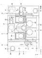
図1〜図3は本発明に係る塗布現像処理システムの全体構成を示す図であり、図1はその平面図、図2は正面図及び図3は背面図である。 1 to 3 are views showing the overall configuration of a coating and developing treatment system according to the present invention. FIG. 1 is a plan view, FIG. 2 is a front view, and FIG. 3 is a rear view.
塗布現像処理システム1は、カセットステーション10、処理ステーション11及びインターフェース部12を一体に接続した構成を有する。カセットステーション10は、被処理基板として半導体ウェハWを、ウェハカセットCRで複数枚例えば25枚単位で、システムに対して外部から搬入又は外部へ搬出する。また、カセットステーション10は、ウェハカセットCRに対してウェハWを搬入・搬出したりする。処理ステーション11は、塗布現像工程の中で1枚ずつウェハWに所定の処理を施す枚葉式の各種処理ユニットを所定位置に多段配置してなる。インターフェース部12は、処理ステーション11と、この処理ステーション11と隣接して設けられる露光装置(図示せず)との間でウェハWを受け渡しする。
The coating and developing
カセットステーション10は、図1に示すように、カセット載置台20、ウェハ搬送体21を有する。カセット載置台20では、カセット載置台20上の突起20aの位置に、複数個例えば4個までのウェハカセットCRが、それぞれのウェハ出入口を処理ステーション11側に向けてX方向一列に載置されている。ウェハ搬送体21は、カセット配列方向(X方向)及びウェハカセットCR内に収納されたウェハのウェハ配列方向(Z方向)に移動可能に設けられている。また、ウェハ搬送体21は、各ウェハカセットCRに選択的にアクセスするようになっている。また、ウェハ搬送体21は、θ方向に回転可能に構成され、後述するように処理ステーション11側の第3の組G3の多段ユニット部に属するアライメントユニット(ALIM)及びイクステンションユニット(EXT)にもアクセスできるようになっている。
As shown in FIG. 1, the
処理ステーション11では、図1に示すように、中心部に垂直搬送型の主ウェハ搬送機構22が設けられ、その周りに全ての処理ユニットが1組または複数の組に亙って多段に配置されている。この例では、5組G1、G2、G3、G4、G5の多段配置構成となっている。第1及び第2の組G1、G2の多段ユニットは、システム正面(図1において手前)側に並置されている。第3の組G3の多段ユニットは、カセットステーション10に隣接して配置されている。第4の組G4の多段ユニットは、インターフェース部12に隣接して配置されている。第5の組G5の多段ユニットは背部側に配置されている。なお第5の組G5は、主ウェハ搬送機構22のメンテナンスのためにレール25に沿って移動可能に構成されている。
In the
図3に示すように、主ウェハ搬送機構22は、ウェハ搬送装置46を上下方向(Z方向)に昇降自在に装備している。筒状支持体49はモータ(図示せず)の回転軸に接続されており、このモータの回転駆動力によって、前記回転軸を中心としてウェハ搬送装置46と一体に回転する。従って、このウェハ搬送装置46は、θ方向に回転自在となっている。ウェハ搬送装置46は、搬送アーム48を有している。
As shown in FIG. 3, the main
図2に示すように、第1の組G1では、カップCP内でウェハWをスピンチャックに載せて所定の処理を行う2台のスピンナ型処理ユニット、例えばレジスト塗布処理ユニット(COT)及び本発明に係る現像処理ユニット(DEV)が下から順に2段に重ねられている。第2の組G2でも、2台のスピンナ型処理ユニット、例えばレジスト塗布処理ユニット(COT)及び現像処理ユニット(DEV)が下から順に2段に重ねられている。レジスト塗布処理ユニット(COT)ではレジスト液の排液が機構的にもメンテナンスの上でも面倒であることから、このように下段に配置するのが好ましい。しかし、必要に応じて上段に配置することも可能である。 As shown in FIG. 2, in the first set G1, two spinner type processing units, such as a resist coating processing unit (COT), which perform predetermined processing by placing a wafer W on a spin chuck in a cup CP and the present invention. The development processing units (DEV) according to are stacked in two stages in order from the bottom. Also in the second group G2, two spinner type processing units, for example, a resist coating processing unit (COT) and a development processing unit (DEV) are stacked in two stages in order from the bottom. In the resist coating processing unit (COT), the drainage of the resist solution is troublesome both in terms of mechanism and maintenance, and thus is preferably arranged in the lower stage. However, it can be arranged in the upper stage as required.
なお、第1の組G1、第2の組G2には、Z方向の下側等の空いたスペースに、レジスト塗布処理ユニット(COT)及び現像処理ユニット(DEV)に各種処理液を供給するためのケミカル室13が設けられてもよい。
The first set G1 and the second set G2 are used for supplying various processing solutions to the resist coating processing unit (COT) and the development processing unit (DEV) in an empty space such as the lower side in the Z direction. The
図3に示すように、第3の組G3では、ウェハWを載置台に載せて所定の処理を行うオーブン型の処理ユニット、例えば下から順にクーリングユニット(COL)、アドヒージョンユニット(AD)、アライメントユニット(ALIM)、イクステンションユニット(EXT)、プリベーキングユニット(PAB)及びポストエクスポージャーベーキングユニット(PEB)が重ねられている。第4の組G4でも、オーブン型の処理ユニット、例えば下から順にクーリングユニット(COL)、イクステンション・クーリングユニット(EXTCOL)、イクステンションユニット(EXT)、プリベーキングユニット(PAB)及びポストエクスポージャーベーキングユニット(PEB)が重ねられている。なお、現像後に加熱処理を行うためのポストベーキングユニットが配置されてもよい。 As shown in FIG. 3, in the third group G3, an oven-type processing unit that performs predetermined processing by placing the wafer W on the mounting table, for example, a cooling unit (COL) and an adhesion unit (AD) in order from the bottom. , An alignment unit (ALIM), an extension unit (EXT), a pre-baking unit (PAB), and a post-exposure baking unit (PEB). Even in the fourth group G4, an oven-type processing unit, for example, a cooling unit (COL), an extension / cooling unit (EXTCOL), an extension unit (EXT), a pre-baking unit (PAB), and a post-exposure baking unit in order from the bottom. (PEB) is superimposed. A post-baking unit for performing a heat treatment after development may be provided.
このように処理温度の低いクーリングユニット(COL)、イクステンション・クーリングユニット(EXTCOL)を下段に配置し、処理温度の高いベーキングユニット(PAB)やポストエクスポージャーベーキングユニット(PEB)を上段に配置する。この上下配置により、ユニット間の熱的な相互干渉を少なくすることができる。しかし、ランダムな多段配置とすることも可能である。 In this way, the cooling unit (COL) and the extension cooling unit (EXTCOL) having a low processing temperature are arranged in the lower stage, and the baking unit (PAB) and the post-exposure baking unit (PEB) having a high processing temperature are arranged in the upper stage. With this vertical arrangement, thermal mutual interference between the units can be reduced. However, a random multistage arrangement is also possible.
インターフェース部12は、奥行方向では処理ステーション11と同じ寸法を有するが、幅方向では小さなサイズにつくられている。インターフェース部12の正面部には可搬性のピックアップカセットCRと定置型のバッファカセットBRが2段に配置され、背面部には周辺露光装置23が配設され、中央部にはウェハ搬送体24が設けられている。このウェハ搬送体24は、X、Z方向に移動して両カセットCR、BR及び周辺露光装置23にアクセスするようになっている。さらに、ウェハ搬送体24は、θ方向に回転可能に構成され、処理ステーション11側の第4の組G4の多段ユニットに属するイクステンションユニット(EXT)にも、及び隣接する露光装置側のウェハ受渡し台(図示せず)にもアクセスできるようになっている。
The
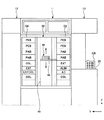
図4及び図5は、本発明の実施の形態に係る現像処理ユニット(DEV)を示す平面図及び断面図である。この現像処理ユニット(DEV)の中央部には、ウェハ搬送装置46の搬送アーム48が進退自在に設けられた環状のカップCΡが配設されている。カップCΡの内側には、ウェハWを水平に保持するスピンチャック52が配置されている。スピンチャック52は真空吸着によってウェハWを固定保持した状態で駆動モータ54によって回転駆動される。駆動モータ54は、ユニット底板50に設けられた開口50aに昇降移動可能に配置され、アルミニウムからなるキャップ状のフランジ部材58を介して、エアシリンダからなる昇降駆動手段60および昇降ガイド手段62と結合されている。このような昇降機構により、主ウェハ搬送機構22との間でウェハWの受け渡しが可能となる。
4 and 5 are a plan view and a cross-sectional view showing the development processing unit (DEV) according to the embodiment of the present invention. At the center of the development processing unit (DEV), an annular cup C is provided in which a
図5に示すように、カップCP内に収容されたウェハW上において、このウェハWの表面に現像液を供給するための現像液ノズル36がノズルスキャンアーム37の先端部に取り付けられている。この現像液ノズル36には供給管31aが接続されており、この供給管31aを介して現像液供給機構31により現像液が供給されるようになっている。この現像液ノズル36は長尺形状を有し、例えば図示しない複数の孔、又はスリット状に形成された供給口より現像液が供給されるようになっている。ノズルスキャンアーム37は、ユニット底板50の上に一方向(Y方向)に敷設されたガイドレール39上で水平移動可能な垂直支持部材40の上端部に取り付けられており、図示しないY方向駆動機構によって垂直支持部材40と一体にY方向に移動するようになっている。また、ノズルスキャンアーム37は垂直支持部材40に沿ってZ方向にも移動可能に構成されており、現像液ノズル36と、スピンチャック52で保持されたウェハWとの距離が調節できるようになっている。
As shown in FIG. 5, on the wafer W accommodated in the cup CP, a
また、ノズル保持体27に保持されウェハW表面にリンス液を供給するためのリンスノズル15が、上記現像液ノズル36と同様に、ノズルスキャンアーム17及び垂直支持部材26により、ガイドレール39に沿ってY方向に移動可能に設けられている。リンスノズル15には供給管32aが接続されており、この供給管32aを介してリンス液供給機構32からリンス液が供給されるようになっている。ここでリンス液としては、例えば純水を使用する。このノズルスキャンアーム17も垂直支持部材26に沿って移動可能に構成されており、リンスノズル15と、スピンチャック52で保持されたウェハWとの距離が調節できるようになっている。
Further, the rinse
カップCPの隣には、ノズル保持体28に保持され、ウェハ上のレジストパターンの表面を疎水化する疎水化剤を、フッ素を含む有機溶剤で希釈してなる処理液を供給するための処理液ノズル16が、ノズルスキャンアーム18の先端に取り付けられている。このノズルスキャンアーム18はモータ19により、このモータ19を中心としてθ方向に回動可能に設けられている。処理液ノズル16には供給管33aが接続されており、この供給管33aを介して処理液供給機構33から処理液が供給されるようになっている。ここで、レジストパターンを疎水化する疎水化剤としては、特に限定されず、例えば、分子中に(CH3)3Siで表されるシリル基を有する化合物を用いることができる。一例として、TMSDMA(トリメチルシリルジメチルアミン)を挙げることができる。また、疎水化剤を希釈するフッ素を含む有機溶剤としては、例えば純水より揮発性の高いハイドロフルオロエーテル(HFE)系溶剤(メチルパーフルオロイソブチルエーテルとメチルパーフルオロブチルエーテルとを混合したもの、又はこれら単独)を使用することができる。また、キシレン、ヘキサメチルジシラザン等も用いることができる。なお、このハイドロフルオロエーテル(HFE)系溶剤は、レジストを溶かさない程度の溶剤であり、レジスト上に供給しても問題はない。
Next to the cup CP, a processing liquid for supplying a processing liquid which is held by the
カップCP内の底部には、ウェハ上に供給された現像液、リンス液及び処理液を排液するための排液管57が設けられており、図示しないシステム外へ排液されるようになっている。また、カップCPの底部には、現像液や処理液の供給により発生したミスト等、カップCP内の雰囲気を排気するための排気管59が設けられており、通常運転時においては真空ポンプ51により常時排気されている状態となっている。
A
また、カップCPには、カップCPの温度を計測する温度センサ64が取り付けられており、更にこのカップCPの温度を調整するための温調ヒータ65が設けられている。この温調ヒータ65は、カップCP全体の温度を所定の温度、通常時には例えば23℃前後に調整するようになっている。
In addition, a
更に、カップCPにおける排気管59及び排液管57にも同様に、排気管59及び排液管57の温度を計測する温度センサ66及び67と、それぞれ排気管59及び排液管57の温度を調整する温調ヒータ68及び69とが取り付けられている。
Further, the
現像液供給機構31、リンス液供給機構32及び処理液供給機構33は、それぞれ制御部30の指令に基づき、現像液、リンス液及び処理液をそれぞれ現像液ノズル36、リンスノズル15及び処理液ノズル16へ供給するようになっている。また、この制御部30は、上記各処理液供給のタイミングの制御とともに、駆動モータ54の回転数を制御するモータコントローラ34に指令を送出し、統括的な処理を行う。
The developing solution supply mechanism 31, the rinsing
また制御部30は、例えば上記温度センサ64、66、67により各部が計測され、この計測された温度が所定の正常範囲内になければ異常とみなし、警告装置45はこれを受けて何らかの警告を行うようになっている。この警告装置としては、例えば警告ブザーや警告灯、あるいは操作ディスプレイ上の警告表示等を用いている。
Further, the
図6は、本発明の実施の形態に係る処理液供給機構を示す図である。処理液供給機構33は、疎水化剤をHFEで希釈してなる処理液を貯蔵する処理液貯蔵タンク71を有する。処理液貯蔵タンク71は、処理液を供給する供給管33aの一端と接続され、供給管33aは、制御部30により開閉制御可能に設けられたバルブ72を介して、前述したように、その他端が処理液ノズル16に接続されている。
FIG. 6 is a diagram showing a processing liquid supply mechanism according to the embodiment of the present invention. The processing
処理液貯蔵タンク71には、処理液を混合して調整するために、HFEを供給するHFE供給管73、TMSDMAである疎水化剤を供給する疎水化剤供給管74の一端が接続されている。また、処理液貯蔵タンク71の内部を加圧して供給管33aに処理液を供給するための例えばN2ガス等の加圧ガス供給管75が接続されている。また、処理液貯蔵タンク71内には、供給された疎水化剤及びHFEを攪拌して混合するための攪拌機構76が設けられている。攪拌機構76は、処理液貯蔵タンク71の内部に設けられた攪拌部77と、処理液貯蔵タンク71の外部に設けられ、攪拌部77を制御部30により制御可能に回転駆動するモータ78とを有している。また、処理液貯蔵タンク71には、貯蔵される処理液の液面の上限と下限とを検知し、制御部30へ検知した信号を送る液面計79が設けられている。
In order to mix and adjust the processing liquid, one end of an
HFE供給管73は、制御部30により開閉制御可能に設けられたバルブ80、同様に制御部30により制御可能に設けられたポンプ81を介して、その他端がHFEを供給するHFE供給源82に接続されている。
The
疎水化剤供給管74は、制御部30により開閉制御可能に設けられたバルブ83を介して、その他端が疎水化剤供給源84に接続されている。疎水化剤供給源84は、HFEに比べて微量の疎水化剤を適量に供給することができ、例えば疎水化剤をシリンジを介して供給するシリンジポンプ85と、制御部30により制御可能に設けられ、シリンジポンプ85を駆動するモータ86とを有している。
The other end of the hydrophobizing
加圧ガス供給管75は、制御部30により開閉制御可能に設けられたバルブ87を介して、その他端が例えばN2ガス等を供給する加圧ガス供給源88に接続されている。
The other end of the pressurized
このようにして構成された処理液供給機構33では、制御部30からの制御に基づいて、バルブ80が開かれ、HFE供給源82からポンプ81を介し、HFE供給管73を通して所定の流量のHFEが処理液貯蔵タンク71に供給される。また、HFEと所定の混合比になるように、制御部30からの制御に基づいて、バルブ83を開き、モータ86に駆動されるシリンジポンプ85から疎水化剤供給管74を通して疎水化剤が処理液貯蔵タンク71に供給される。供給されたHFE及び疎水化剤は、攪拌機構76により均一に攪拌され、処理液貯蔵タンク71に貯蔵される。このような処理液貯蔵タンク71へのHFE及び疎水化剤の供給及び混合は、連続的又は断続的に行われ、液面計79により検知される液面が上限及び下限の間にあるように、その液量が、保持される。
In the processing
このようにして処理液が貯蔵された処理液貯蔵タンク71から処理液ノズル16に処理液を供給する際には、バルブ87が開かれ、加圧ガス供給源88から加圧ガス供給管75を通って処理液貯蔵タンク71に加圧ガスが供給される。そして、バルブ72が開かれ、供給管33aを通して処理液ノズル16に処理液を供給する。一方、処理液ノズル16への処理液の供給を停止するときは、供給管33aのバルブ72を閉じるとともに、バルブ87を閉じ、加圧ガス供給源88からの加圧ガスの供給も停止する。
When supplying the processing liquid from the processing
次に、以上説明した塗布現像処理システム1の一連の処理工程について説明する。
Next, a series of processing steps of the coating and developing
先ず、カセットステーション10において、ウェハ搬送体21がカセット載置台20上の処理前のウェハを収容しているカセットCRにアクセスして、そのカセットCRから1枚のウェハWを取り出す。取り出されたウェハWは、アライメントユニット(ALIM)に搬送され、位置合わせが行われる。その後、ウェハWは、主ウェハ搬送機構22によりアドヒージョンユニット(AD)へ搬送されて疎水化処理が行われ、次いでクーリングユニット(COL)に搬送されて所定の冷却処理が行われる。その後、レジスト塗布処理ユニット(COT)に搬送されてレジスト塗布処理が行われ、プリベーキングユニット(PAB)に搬送されて所定の加熱処理が行われ、クーリングユニット(COL)に搬送されて所定の冷却処理が行われる。その後、ウェハ搬送体24によりインターフェース部12を介して図示しない露光装置に搬送されて露光処理が行われる。露光処理が終了したウェハWは、ポストエクスポージャーベーキングユニット(PEB)に搬送されて所定の加熱処理が行われ、次に現像処理ユニット(DEV)に搬送されて現像処理が行われる。現像処理後に、所定の加熱処理(ポストベーキング)が行われることもある。その後、ウェハWは、クーリングユニット(COL)に搬送されて所定の冷却処理が行われ、エクステンションユニット(EXT)を介してカセットCRに戻される。
First, in the
次に、図7から図11を参照して、現像処理ユニットを用いた現像処理方法について説明する。図7は各工程の手順を説明するためのフローチャートである。図8から図10は各工程を行う際の側面図であり、図11は、現像処理の際のレジストパターンを示す拡大断面図である。 Next, a development processing method using the development processing unit will be described with reference to FIGS. FIG. 7 is a flowchart for explaining the procedure of each step. 8 to 10 are side views when performing each process, and FIG. 11 is an enlarged cross-sectional view showing a resist pattern at the time of development processing.
図7に示すように、本実施の形態に係る現像処理方法は、現像液供給工程(ステップS11)、現像液除去工程(ステップS12)、リンス液供給工程(ステップS13)、処理液供給工程(ステップS14〜ステップS16)、疎水化処理安定化工程(ステップS17)、処理液除去工程(ステップS18及びステップS19)及び乾燥処理工程(ステップS20)を有する。処理液供給工程は、第1の供給工程(ステップS14)、第2の供給工程(ステップS15)及び第3の供給工程(ステップS16)を有する。処理液除去工程は、第1の除去工程(ステップS18)及び第2の除去工程(ステップS19)を有する。 As shown in FIG. 7, the development processing method according to the present embodiment includes a developer supply process (step S11), a developer removal process (step S12), a rinse liquid supply process (step S13), and a process liquid supply process ( Step S14 to Step S16), a hydrophobization treatment stabilization step (Step S17), a treatment liquid removal step (Step S18 and Step S19), and a drying treatment step (Step S20). The treatment liquid supply process includes a first supply process (step S14), a second supply process (step S15), and a third supply process (step S16). The treatment liquid removal step includes a first removal step (step S18) and a second removal step (step S19).
また、図7に示す現像処理方法が実施する処理レシピの例を表1に示す。 Table 1 shows an example of a processing recipe executed by the development processing method shown in FIG.

最初に、現像液供給工程(ステップS11)を行う。現像液供給工程(ステップS11)では、基板に現像液を供給し、レジストパターンを現像する。 First, a developer supply process (step S11) is performed. In the developer supply process (step S11), the developer is supplied to the substrate to develop the resist pattern.
先ず、スピンチャック52が上昇し、主ウェハ搬送機構22からウェハWを受け取ると、スピンチャック52が下降しウェハWがカップCP内に収容される。そして、図8(a)に示すように現像液ノズル36が現像液41を吐出しながらウェハW上を移動し、吐出が終了した後にウェハWを例えば60秒放置し現像処理を進行させる。ここで高スループット化を図るため、ウェハWを回転させながら現像液41を吐出しても構わない。そのときは、ウェハWを所定の回転数で回転させて現像液41を伸展させ、例えば60秒間放置することにより現像処理を進行させることになる。
First, when the
次に、現像液除去工程(ステップS12)を行う。現像液除去工程(ステップS12)では、レジストパターンが現像された基板上に、リンス液を供給し、基板上から現像液を除去する。 Next, a developer removing process (step S12) is performed. In the developer removing step (Step S12), a rinse solution is supplied onto the substrate on which the resist pattern has been developed, and the developer is removed from the substrate.
図8(b)に示すように、現像液ノズル36をカップ外へ移動させ、リンスノズル15をウェハWの中心上へ移動させる。そして、図8(c)に示すように、ウェハWを回転させながらリンス液42を吐出し、現像液41を洗い流す。このとき、ウェハWを回転させながら行うため、現像液41を振り切りながら純水でウェハWの表面をリンス液42でリンスすることになる。
As shown in FIG. 8B, the
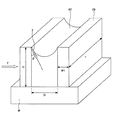
図11(a)に示すように、現像されたレジストパターン29の上面29aがリンス液42から出ないようにするために、ウェハWの回転数を低速の300rpm〜800rpm、より好ましくは500rpmとする。レジストパターン29の上面29aがリンス液42から出てしまうと、リンス液42の表面張力によりパターン倒れが生じるおそれがあるためである。このようにウェハWの回転を300rpm〜800rpmの比較的低速回転とすることにより、ウェハW上で流れるリンス液42の速度を極力小さくして、現像液41を洗い流すときにレジストパターン29が倒れないようにする。なお、以下では、レジストパターンのことを「パターン」ということがある。
As shown in FIG. 11A, in order to prevent the
次に、リンス液供給工程(ステップS13)を行う。リンス液供給工程(ステップS13)では、基板を次の第1の供給工程における回転数(第1の回転数)R1よりも低い第4の回転数R4で回転させながら、リンス液を供給する。 Next, a rinse liquid supply process (step S13) is performed. In the rinse liquid supply process (step S13), the rinse liquid is supplied while rotating the substrate at the fourth rotation speed R4 lower than the rotation speed (first rotation speed) R1 in the next first supply process.
現像液除去工程(ステップS12)において、リンス液42でリンスされたウェハWの表面が、次の処理液供給工程(ステップS14〜ステップS16)において処理液が供給されるまでに乾燥しないように、すなわち液切れしないように、ウェハWの表面にリンス液(純水)の液膜(純水パドル)を形成する。図8(d)に示すように、ウェハWの回転数R4(本発明における第4の回転数に相当する。)を0rpm〜300rpm、より好ましくは100rpmとする。
In the developer removing process (step S12), the surface of the wafer W rinsed with the rinse
次に、処理液供給工程(ステップS14〜ステップS16)を行う。処理液供給工程(ステップS14〜ステップS16)では、レジストパターンが現像された後、リンス液が供給された基板上に、レジストパターンを疎水化する疎水化剤がハイドロフルオロエーテル(HFE)で希釈されてなる処理液を供給する。また、処理液供給工程(ステップS14〜ステップS16)は、前述したように、第1の供給工程(ステップS14)、第2の供給工程(ステップS15)及び第3の供給工程(ステップS16)を有する。 Next, a process liquid supply process (steps S14 to S16) is performed. In the treatment liquid supply process (steps S14 to S16), after the resist pattern is developed, a hydrophobizing agent that hydrophobizes the resist pattern is diluted with hydrofluoroether (HFE) on the substrate supplied with the rinse liquid. Supply the treatment liquid. Further, as described above, the treatment liquid supply process (steps S14 to S16) includes the first supply process (step S14), the second supply process (step S15), and the third supply process (step S16). Have.
まず、第1の供給工程(ステップS14)を行う。第1の供給工程(ステップS14)では、基板を第1の回転数R1で回転させながら、基板上に処理液を供給する。 First, a 1st supply process (step S14) is performed. In the first supply process (step S14), the processing liquid is supplied onto the substrate while rotating the substrate at the first rotation speed R1.
図9(a)に示すように、リンスノズル15をカップ外へ移動させ、処理液ノズル16をウェハWの中心上へ移動させる。そして、図9(b)に示すように、ウェハWを300rpm〜500rpm、より好ましくは400rpmで回転させ、ウェハWの中心上に処理液43を吐出する。すなわち、第1の回転数R1は、300rpm〜500rpmである。第1の回転数R1が300rpmより低いときは、処理液43がウェハW上のリンス液42に対して均一に混ざらず、処理液43が粒状になってリンス液42中に散在してしまい、このままウェハWの回転による振り切り乾燥を行うとパターン倒れが生じてしまう。一方、第1の回転数R1が500rpmより高いときは、処理液43が均一に伸展するが、処理液43が伸展する前にウェハW上からリンス液42が流れ出し、パターン倒れを引き起こす可能性が高い。
As shown in FIG. 9A, the rinse
次に、第2の供給工程(ステップS15)を行う。第2の供給工程(ステップS15)では、基板を第1の回転数R1よりも高い第2の回転数R2で回転させながら、基板上に処理液を供給する。 Next, a 2nd supply process (step S15) is performed. In the second supply process (step S15), the processing liquid is supplied onto the substrate while rotating the substrate at the second rotation speed R2 higher than the first rotation speed R1.
図9(c)に示すように、ウェハWを1000rpm〜1500rpm、より好ましくは1200rpmで回転させ、図11(b)に示すように、ウェハW上に残存していたリンス液42を処理液43に置換する。このように、ウェハWを高速の1000rpm〜1500rpmで回転させて処理液43で置換することにより、ウェハWの全面に処理液43を伸展させつつ、ウェハW上からリンス液42が流れ出る際のパターン倒れを防止することができる。
As shown in FIG. 9C, the wafer W is rotated at 1000 rpm to 1500 rpm, more preferably 1200 rpm, and the rinse
次に、第3の供給工程(ステップS16)を行う。第3の供給工程(ステップS16)では、基板を第2の回転数R2よりも低い第3の回転数R3で回転させながら、基板上に処理液を供給する。 Next, a 3rd supply process (step S16) is performed. In the third supply step (step S16), the processing liquid is supplied onto the substrate while rotating the substrate at a third rotation speed R3 lower than the second rotation speed R2.
図9(d)に示すように、ウェハWを0rpm〜500rpm、より好ましくは300rpmで回転させ、図11(c)に示すように、レジストパターン29上の処理液43の液量を調整する。このように、ウェハWを低速の0rpm〜500rpmで回転させることにより、ウェハW上の処理液43の液量を調整することができる。すなわち、第3の回転数R3は、0rpm〜500rpmである。第3の回転数R3が500rpmより高いときは、処理液43がウェハW上から振り切られてしまい、処理液43の液量が少なくなってしまう。
As shown in FIG. 9D, the wafer W is rotated at 0 rpm to 500 rpm, more preferably 300 rpm, and the amount of the
次に、疎水化処理安定化工程(ステップS17)を行う。疎水化処理安定化工程(ステップS17)では、処理液の供給を停止し、基板の回転を略停止した状態で、レジストパターンの疎水化処理を安定化させる。 Next, a hydrophobization treatment stabilization step (step S17) is performed. In the hydrophobizing treatment stabilization step (step S17), the resist pattern hydrophobizing treatment is stabilized while the supply of the processing liquid is stopped and the rotation of the substrate is substantially stopped.
図10(a)に示すように、処理液43の吐出を停止し、処理液ノズル16をカップ外へ移動させ、ウェハWの回転数を0〜50rpmにするか、より好ましくは回転を停止させ、ウェハWを略静止させた状態で、ウェハWの全面でレジストパターン29の表面の疎水化処理を安定化させる。
As shown in FIG. 10A, the discharge of the
次に、処理液除去工程(ステップS18及びステップS19)を行う。処理液除去工程(ステップS18及びステップS19)では、処理液が供給された基板上から、処理液を除去する。また、処理液除去工程(ステップS18及びステップS19)は、前述したように、第1の除去工程(ステップS18)及び第2の除去工程(ステップS19)を有する。 Next, a process liquid removal process (step S18 and step S19) is performed. In the processing liquid removal step (step S18 and step S19), the processing liquid is removed from the substrate supplied with the processing liquid. Further, as described above, the treatment liquid removal process (step S18 and step S19) includes the first removal process (step S18) and the second removal process (step S19).
まず、第1の除去工程(ステップS18)を行う。第1の除去工程(ステップS18)では、基板を第5の回転数R5で回転させながら、基板上から処理液を除去する。 First, the first removal process (step S18) is performed. In the first removal step (step S18), the processing liquid is removed from the substrate while rotating the substrate at the fifth rotation speed R5.
図10(b)に示すように、ウェハWを300rpm〜700rpm、より好ましくは500rpmで回転させる。このように、ウェハWを低速の300rpm〜700rpmで回転させることにより、ウェハWの表面の処理液43を少し除去することができる。ここで、必要に応じて純水よりなるリンス液42をウェハ中央付近から吐出させながら処理液43を除去してもよい。
As shown in FIG. 10B, the wafer W is rotated at 300 rpm to 700 rpm, more preferably at 500 rpm. Thus, the
次に、第2の除去工程(ステップS19)を行う。第2の除去工程(ステップS19)では、基板を第5の回転数R5よりも高い第6の回転数R6で回転させながら、基板上から処理液を除去する。 Next, a second removal process (step S19) is performed. In the second removal step (step S19), the processing liquid is removed from the substrate while rotating the substrate at a sixth rotational speed R6 that is higher than the fifth rotational speed R5.
図10(c)に示すように、ウェハWを1000rpm〜1500rpm、より好ましくは1200rpmで回転させる。このように、ウェハWを高速の1000rpm〜1500rpmで回転させることにより、ウェハW表面の処理液43を効率良く除去することができる。また、必要に応じて純水よりなるリンス液42をウェハ中央付近から吐出させながら処理液43を除去してもよいのは、第1の除去工程と同様である。
As shown in FIG. 10C, the wafer W is rotated at 1000 rpm to 1500 rpm, more preferably 1200 rpm. Thus, the
図11(d)に示す処理液43のレジストパターン29に対する接触角θは、85°〜95°となっており、処理液43がパターン間から抜け出ても表面張力は小さいので、パターン倒れを起こすことはない。より好ましい接触角θは、図14を用いて後述するように、90°〜95°である。このような高い接触角は、処理液43が、疎水化剤であるTMSDMAを、表面張力がリンス液の表面張力よりも小さいHFEで希釈してなるものであるために、達成できる。また、いったん疎水化処理が行われた後は、純水よりなるリンス液42に対しても、このような高い接触角が達成できる。TMSDMAは、後述するように、疎水性を有するシリル基等の疎水基を有しており、レジストパターン29の表面をシリル基等の疎水基で置換する。また、HFEは、後述するように、フッ素を有しているため、レジストパターン29の表面をフッ素でコーティングする。これらによって、上記接触角が実現できる。
The contact angle θ of the
また、HFEは、純水より比重が大きいため、図9(c)における処理液43の供給の際に、処理液43がリンス液42より下部に配置されるようになり、リンス液42がレジストパターン29間から抜け出易くなる。従って、パターン倒れの防止は、よりいっそう効果的となる。
Further, since HFE has a higher specific gravity than pure water, the
そして、最後に乾燥処理工程(ステップS20)を行う。乾燥処理工程(ステップS20)では、基板を所定の回転数で回転させ乾燥処理を行う。 Finally, a drying process (step S20) is performed. In the drying process (step S20), the substrate is rotated at a predetermined rotational speed to perform the drying process.
図10(d)に示すように、ウェハWを1500rpm〜2500rpm、より好ましくは2000rpmの高回転で回転させ、ウェハWの表面を十分に乾燥させる。 As shown in FIG. 10D, the wafer W is rotated at a high rotation speed of 1500 rpm to 2500 rpm, more preferably 2000 rpm, and the surface of the wafer W is sufficiently dried.
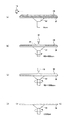
次に、本実施の形態で、処理液がレジストパターンのパターン倒れを防止する作用効果について説明する。 Next, in this embodiment, an effect of the processing liquid preventing the pattern pattern from falling down will be described.
図12は、パターンの間にリンス液が存在するときに、リンス液の接触角とパターンを倒そうとする力との関係を説明するための図である。2本のレジストパターン29の間をリンス液42でリンスした後、リンス液42を乾燥していく途中の段階では、図12に示すように、あるレジストパターン29の一方の側がリンス液42と接触し、一方の側が乾燥して空気と接触した状態となる。このような状態が形成されると、レジストパターン29の一方の側からはリンス液42に押され、他方の側から空気に押されるため、その圧力差があると、レジストパターン29を倒そうとする力が働くことになる。このパターンを倒そうとする力Fは、次式(1)で表される。
FIG. 12 is a diagram for explaining the relationship between the contact angle of the rinsing liquid and the force for defeating the pattern when the rinsing liquid is present between the patterns. After rinsing between the two resist
本実施の形態に係る現像処理方法は、上記したうちの(4)接触角θを大きくすることによって、パターンにかかる最大応力σMAXを低減し、パターン倒れを防止するものである。 In the development processing method according to the present embodiment, the maximum stress σ MAX applied to the pattern is reduced and the pattern collapse is prevented by increasing the contact angle θ of (4) above.
図13は、TMSDMAをTFEで希釈してなる処理液が、レジストパターンの表面を疎水化する疎水化処理における反応メカニズムを説明する図である。処理液に含まれるTMSDMA(トリメチルシリルジメチルアミン)は、その分子中に(CH3)3Siで表されるシリル基を有する。一方、レジストは、その高分子構造中にOH基を有する。TMSDMA中のシリル基がレジストパターンの表面において、レジスト中のOH基のHと置換反応を起こす。OH基が親水基であるのに対し、OH基のHがシリル基と置換した基は疎水基である。従って、レジストパターン表面に形成された疎水基によって、レジストパターンの表面が疎水化される。 FIG. 13 is a diagram for explaining a reaction mechanism in a hydrophobic treatment in which a treatment liquid obtained by diluting TMSDMA with TFE hydrophobizes the surface of a resist pattern. TMSDMA (trimethylsilyldimethylamine) contained in the treatment liquid has a silyl group represented by (CH 3 ) 3 Si in the molecule. On the other hand, the resist has an OH group in its polymer structure. The silyl group in TMSDMA causes a substitution reaction with H of the OH group in the resist on the surface of the resist pattern. While the OH group is a hydrophilic group, the group in which H of the OH group is substituted with a silyl group is a hydrophobic group. Therefore, the surface of the resist pattern is hydrophobized by the hydrophobic groups formed on the resist pattern surface.
次に、図14及び表2から表4を参照し、本実施の形態に係る現像処理方法によるパターン倒れ防止効果についての評価結果について説明する。
(実施例1)
実施例1として、図7に示すステップS11からステップS20の各工程を行った。ステップS13からステップS20の各工程の条件は、表1に示す処理レシピの例に従って実施した。ただし、表1のステップS14からステップS16で供給する処理液として、TMSDMAをHFE:TMSDMA=100:1の混合比で希釈した処理液を用いた。
(比較例1)
比較例1として、処理液の種類を変更した以外は、実施例1と同様にして、図7に示すステップS11からステップS20の各工程を行った。比較例1では、ステップS14からステップS16で供給する処理液として、TMSDMAを含まないHFEよりなる処理液を用いた。
(比較例2)
比較例2として、処理液供給工程及び疎水化安定化工程を行わず、リンス液(純水)のみでリンスする現像処理方法を行った。すなわち、表1に示す処理レシピのうちステップS13からステップS17を省略し、図7に示すステップS11、ステップS12、ステップS18からステップS20の各工程を行った。
Next, with reference to FIG. 14 and Tables 2 to 4, evaluation results on the pattern collapse prevention effect by the development processing method according to the present embodiment will be described.
Example 1
As Example 1, steps S11 to S20 shown in FIG. 7 were performed. The conditions of each step from step S13 to step S20 were performed according to the processing recipe example shown in Table 1. However, as the processing liquid supplied in steps S14 to S16 in Table 1, a processing liquid in which TMSDMA was diluted with a mixing ratio of HFE: TMSDMA = 100: 1 was used.
(Comparative Example 1)
As Comparative Example 1, steps S11 to S20 shown in FIG. 7 were performed in the same manner as in Example 1 except that the type of the treatment liquid was changed. In Comparative Example 1, a treatment liquid made of HFE not containing TMSDMA was used as the treatment liquid supplied from Step S14 to Step S16.
(Comparative Example 2)
As Comparative Example 2, a development processing method was performed in which the treatment liquid supply step and the hydrophobization stabilization step were not performed, and the rinse was performed only with a rinse solution (pure water). That is, Steps S13 to S17 in the processing recipe shown in Table 1 were omitted, and Steps S11, S12, and Steps S18 to S20 shown in FIG. 7 were performed.
実施例1、比較例1、比較例2のそれぞれを行った後のレジストパターンについて、レジストパターンと同じレジストの塗布膜を疎水化処理し、その表面の接触角を測定した。測定方法として、その表面に純水を滴下し(0.1ml)、その接触角を、側面から専用のカメラで撮影して測定する方法を用いた。その結果を、図14のグラフに示す。 With respect to the resist pattern after performing each of Example 1, Comparative Example 1, and Comparative Example 2, the same resist coating film as the resist pattern was subjected to a hydrophobic treatment, and the contact angle of the surface was measured. As a measuring method, pure water was dropped on the surface (0.1 ml), and the contact angle was measured by photographing with a dedicated camera from the side. The result is shown in the graph of FIG.
図14に示すように、実施例1、比較例1、比較例2のそれぞれにおいて、接触角θは、93.5°、78.5°、80.9°となった。すなわち、実施例1において、比較例1、比較例2よりも大きな接触角θが得られた。従って、前述したように、実施例1において、比較例1、比較例2よりもパターンにかかる最大応力σMAXを小さくすることができることが明らかになった。 As shown in FIG. 14, in each of Example 1, Comparative Example 1, and Comparative Example 2, the contact angles θ were 93.5 °, 78.5 °, and 80.9 °. That is, in Example 1, a larger contact angle θ was obtained than in Comparative Examples 1 and 2. Therefore, as described above, in Example 1, it became clear that the maximum stress σ MAX applied to the pattern can be made smaller than those in Comparative Example 1 and Comparative Example 2.
実施例1は、処理液を用いない比較例2に対してのみならず、HFEよりなる処理液を用いた比較例1に対しても、接触角が増大している。これは、疎水化剤を含まず単にHFEよりなる処理液でレジスト表面をフッ素処理しても、接触角はあまり増大しないことを示している。また、HFE:TMSDMA=100:1の混合比を有する処理液では、接触角を90°以上にすることができる。
(実施例2)
実施例2として、露光時のベストフォーカス位置からフォーカス位置をずらし、かつ、露光時のドーズ量を変更したこと以外は、実施例1と同様にして、図7に示すステップS11からステップS20の各工程を行った。パターンとしては、ライン幅120nm及びスペース幅120nm(ピッチ240nm)、並びに高さ380nmを有するレジストパターンを形成した。各フォーカス位置のずれ量及び各ドーズ量の条件に対応して得られたパターンの線幅であるCD(Critical Dimension)値を、走査型電子顕微鏡SEM(Scanning Electron Microscope)を用いて測定した。これらの値を表2に示す。
In Example 1, the contact angle is increased not only for Comparative Example 2 that does not use the treatment liquid but also for Comparative Example 1 that uses the treatment liquid made of HFE. This indicates that the contact angle does not increase so much even if the resist surface is fluorine treated with a processing solution that does not contain a hydrophobizing agent and is simply made of HFE. Moreover, in the processing liquid which has a mixing ratio of HFE: TMSDMA = 100: 1, a contact angle can be 90 degrees or more.
(Example 2)
As Example 2, each of steps S11 to S20 shown in FIG. 7 is performed in the same manner as in Example 1 except that the focus position is shifted from the best focus position at the time of exposure and the dose amount at the time of exposure is changed. The process was performed. As the pattern, a resist pattern having a line width of 120 nm, a space width of 120 nm (pitch 240 nm), and a height of 380 nm was formed. The CD (Critical Dimension) value, which is the line width of the pattern obtained corresponding to the conditions of the shift amount of each focus position and each dose amount, was measured using a scanning electron microscope SEM (Scanning Electron Microscope). These values are shown in Table 2.
(比較例3)
比較例3として、露光時のベストフォーカス位置からフォーカス位置をずらし、かつ、露光時のドーズ量を変更したこと以外は、比較例1と同様にして行った。また、パターンとしては、実施例2と同様に、ライン幅120nm及びスペース幅120nm(ピッチ240nm)、並びに高さ380nmを有するレジストパターンを形成した。比較例1と同様に、ステップS14からステップS16で供給する処理液として、TMSDMAを含まないHFEよりなる処理液を用いた。各フォーカス位置のずれ量及び各ドーズ量の条件に対応して得られたパターンのCD値を表3に示す。
(Comparative Example 3)
Comparative Example 3 was performed in the same manner as Comparative Example 1 except that the focus position was shifted from the best focus position during exposure and the dose amount during exposure was changed. Further, as a pattern, a resist pattern having a line width of 120 nm, a space width of 120 nm (pitch 240 nm), and a height of 380 nm was formed as in Example 2. Similar to Comparative Example 1, a processing liquid made of HFE not containing TMSDMA was used as the processing liquid supplied in steps S14 to S16. Table 3 shows the CD values of the patterns obtained corresponding to the conditions of the shift amounts of the focus positions and the dose amounts.
(比較例4)
比較例4として、露光時のベストフォーカス位置からフォーカス位置をずらし、かつ、露光時のドーズ量を変更したこと以外は、比較例2と同様にして行った。また、パターンとしては、実施例2と同様に、ライン幅120nm及びスペース幅120nm(ピッチ240nm)、並びに高さ380nmを有するレジストパターンを形成した。比較例2と同様に、処理液供給工程及び疎水化安定化工程を行わず、リンス液(純水)のみでリンスする現像処理方法を行った。各フォーカス位置のずれ量及び各ドーズ量の条件に対応して得られたパターンのCD値を表4に示す。
(Comparative Example 4)
Comparative Example 4 was performed in the same manner as Comparative Example 2 except that the focus position was shifted from the best focus position during exposure and the dose amount during exposure was changed. Further, as a pattern, a resist pattern having a line width of 120 nm, a space width of 120 nm (pitch 240 nm), and a height of 380 nm was formed as in Example 2. As in Comparative Example 2, the development processing method was performed in which the treatment liquid supply step and the hydrophobization stabilization step were not performed, and the rinse was performed only with the rinse liquid (pure water). Table 4 shows the CD values of the patterns obtained corresponding to the conditions of the shift amounts of the focus positions and the dose amounts.
表2から表4を比較すると、実施例2においては、比較例3、比較例4よりもパターン倒れを防止できることが明らかである。これは、前述したように、TMSDMAがレジストパターンの表面のOH基のHをシリル基で置換して疎水性を増大させ、パターンでのリンス液に対する接触角θを増大させ、パターンにかかる最大応力σMAXを減少させるためである。 Comparing Table 2 to Table 4, it is clear that in Example 2, pattern collapse can be prevented more than in Comparative Examples 3 and 4. As described above, this is because TMSDMA replaces H of the OH group on the surface of the resist pattern with a silyl group to increase the hydrophobicity, increase the contact angle θ with respect to the rinsing liquid in the pattern, and increase the maximum stress applied to the pattern. This is to reduce σ MAX .
なお、実施例1、実施例2を行うにあたり、TMSDMAをHFE:TMSDMA=300:1の混合比で希釈した処理液を用いて行ったときも、実施例1、実施例2と略同等の効果が得られた。 In addition, when performing Example 1 and Example 2, when performing using the process liquid which diluted TMSDMA by the mixing ratio of HFE: TMSDMA = 300: 1, an effect substantially equivalent to Example 1 and Example 2 is carried out. was gotten.
一方、処理液におけるTMSDMAの混合比(濃度)を、HFE:TMSDMA=100:1程度よりも増大させたときには、パターン倒れを防止する効果が向上することはなく、かつ、処理液のコストが増大する。これは、TMSDMA自体がレジストを溶解させる性質を有しているためであり、また、TMSDMAが高価な薬液であるためである。 On the other hand, when the mixing ratio (concentration) of TMSDMA in the processing liquid is increased to be higher than about HFE: TMSDMA = 100: 1, the effect of preventing pattern collapse is not improved, and the cost of the processing liquid increases. To do. This is because TMSDMA itself has a property of dissolving the resist, and TMSDMA is an expensive chemical solution.
従って、パターン倒れを防止し、かつ、コストの増大を抑制することができる処理液の混合比としては、HFE:TMSDMA=100:1からHFE:TMSDMA=300:1程度の範囲であることが好ましい。 Therefore, the mixing ratio of the processing solutions that can prevent pattern collapse and suppress cost increase is preferably in the range of about HFE: TMSDMA = 100: 1 to about HFE: TMSDMA = 300: 1. .
以上、本発明の好ましい実施の形態について記述したが、本発明はかかる特定の実施の形態に限定されるものではなく、特許請求の範囲内に記載された本発明の要旨の範囲内において、種々の変形・変更が可能である。 The preferred embodiments of the present invention have been described above, but the present invention is not limited to such specific embodiments, and various modifications can be made within the scope of the gist of the present invention described in the claims. Can be modified or changed.
1 塗布現像処理システム
15 リンスノズル
16 処理液ノズル
29 レジストパターン
31 現像液供給機構
32 リンス液供給機構
33 処理液供給機構
36 現像液ノズル
41 現像液
42 リンス液
43 処理液
52 スピンチャック
DESCRIPTION OF
Claims (12)
前記処理液が供給された前記基板上から、前記処理液を除去する処理液除去工程と
を有し、
前記処理液供給工程は、
前記基板を第1の回転数で回転させながら、前記基板上に前記処理液を供給する第1の供給工程と、
前記第1の供給工程の後に、前記基板を前記第1の回転数よりも高い第2の回転数で回転させながら、前記基板上に前記処理液を供給する第2の供給工程と、
前記第2の供給工程の後に、前記基板を前記第2の回転数よりも低い第3の回転数で回転させながら、前記基板上に前記処理液を供給する第3の供給工程と
を有する、現像処理方法。 After the resist pattern is developed, a treatment liquid supply step of supplying a treatment liquid obtained by diluting a hydrophobizing agent with a hydrophobizing agent that hydrophobizes the resist pattern on a substrate supplied with a rinsing liquid;
From the treatment liquid supplied on the substrate, it has a treatment liquid removing step of removing the processing solution,
The treatment liquid supply step includes
A first supply step of supplying the processing liquid onto the substrate while rotating the substrate at a first rotational speed;
A second supply step of supplying the processing liquid onto the substrate while rotating the substrate at a second rotation number higher than the first rotation number after the first supply step;
A third supply step for supplying the processing liquid onto the substrate while rotating the substrate at a third rotational speed lower than the second rotational speed after the second supply step;
A development processing method.
前記処理液の供給を停止し、前記基板の回転を略停止した状態で、前記レジストパターンの疎水化処理を安定化させる疎水化処理安定化工程を有する、請求項1に記載の現像処理方法。 After the treatment liquid supply step and before the treatment liquid removal step,
The development processing method according to claim 1, further comprising a hydrophobizing treatment stabilization step of stabilizing the hydrophobizing treatment of the resist pattern in a state where the supply of the processing liquid is stopped and the rotation of the substrate is substantially stopped.
前記基板を前記第1の回転数よりも低い第4の回転数で回転させながら、前記基板上に前記リンス液を供給するリンス液供給工程を有する、請求項1から請求項3のいずれか一項に記載の現像処理方法。 Before the treatment liquid supply step,
While rotating the substrate at a rotational speed of said first lower than the rotational speed 4th, having a rinse solution supply step of supplying the rinse liquid on the substrate, any one of claims 1 to 3 one The development processing method according to item .
前記基板を第5の回転数で回転させながら、前記基板上から前記処理液を除去する第1の除去工程と、
前記第1の除去工程の後に、前記基板を前記第5の回転数よりも高い第6の回転数で回転させながら、前記基板上から前記処理液を除去する第2の除去工程と
を有する、請求項1から請求項4のいずれか一項に記載の現像処理方法。 The treatment liquid removing step includes
A first removal step of removing the processing liquid from the substrate while rotating the substrate at a fifth rotational speed;
A second removal step of removing the processing liquid from the substrate while rotating the substrate at a sixth rotational speed higher than the fifth rotational speed after the first removal step; The development processing method according to any one of claims 1 to 4 .
前記基板の表面上を疎水化する疎水化剤がハイドロフルオトエーテルで希釈されてなる処理液を供給する処理液供給工程と、
前記処理液が供給された前記基板上から、前記処理液を除去する処理液除去工程と
を有し、
前記処理液供給工程は、
前記基板を第1の回転数で回転させながら、前記基板上に前記処理液を供給する第1の供給工程と、
前記第1の供給工程の後に、前記基板を前記第1の回転数よりも高い第2の回転数で回転させながら、前記基板上に前記処理液を供給する第2の供給工程と、
前記第2の供給工程の後に、前記基板を前記第2の回転数よりも低い第3の回転数で回転させながら、前記基板上に前記処理液を供給する第3の供給工程と
を有する、基板処理方法。 A substrate processing method including a step of supplying a rinse liquid when processing a substrate,
A treatment liquid supply step of supplying a treatment liquid obtained by diluting a hydrophobizing agent with a hydrophobizing agent that hydrophobizes the surface of the substrate;
From the treatment liquid supplied on the substrate, it has a treatment liquid removing step of removing the processing solution,
The treatment liquid supply step includes
A first supply step of supplying the processing liquid onto the substrate while rotating the substrate at a first rotational speed;
A second supply step of supplying the processing liquid onto the substrate while rotating the substrate at a second rotation number higher than the first rotation number after the first supply step;
A third supply step for supplying the processing liquid onto the substrate while rotating the substrate at a third rotational speed lower than the second rotational speed after the second supply step;
A substrate processing method.
前記処理液の供給を停止し、前記基板の回転を略停止した状態で、前記レジストパターンの疎水化処理を安定化させる疎水化処理安定化工程を有する、請求項7に記載の基板処理方法。 After the treatment liquid supply step and before the treatment liquid removal step,
The substrate processing method according to claim 7 , further comprising a hydrophobizing treatment stabilization step of stabilizing the hydrophobizing treatment of the resist pattern in a state where supply of the processing liquid is stopped and rotation of the substrate is substantially stopped.
前記基板を前記第1の回転数よりも低い第4の回転数で回転させながら、前記基板上に前記リンス液を供給するリンス液供給工程を有する、請求項7から請求項9のいずれか一項に記載の基板処理方法。 Before the treatment liquid supply step,
10. The rinsing liquid supply step of supplying the rinsing liquid onto the substrate while rotating the substrate at a fourth rotational speed lower than the first rotational speed . 10. The substrate processing method according to item .
前記基板を第5の回転数で回転させながら、前記基板上から前記処理液を除去する第1の除去工程と、
前記第1の除去工程の後に、前記基板を前記第5の回転数よりも高い第6の回転数で回転させながら、前記基板上から前記処理液を除去する第2の除去工程と
を有する、請求項7から請求項10のいずれか一項に記載の基板処理方法。 The treatment liquid removing step includes
A first removal step of removing the processing liquid from the substrate while rotating the substrate at a fifth rotational speed;
A second removal step of removing the processing liquid from the substrate while rotating the substrate at a sixth rotational speed higher than the fifth rotational speed after the first removal step; The substrate processing method as described in any one of Claims 7-10.
Said processing liquid removing step, while supplying a rinsing liquid onto the substrate, the substrate processing method according to any one of claims 11 claim 7.
Priority Applications (5)
| Application Number | Priority Date | Filing Date | Title |
|---|---|---|---|
| JP2009230642A JP5437763B2 (en) | 2009-10-02 | 2009-10-02 | Development processing method and substrate processing method |
| TW099123301A TWI459159B (en) | 2009-10-02 | 2010-07-15 | Developing processing method and substrate processing method |
| US13/499,362 US8691497B2 (en) | 2009-10-02 | 2010-08-20 | Developing treatment method |
| PCT/JP2010/064038 WO2011040140A1 (en) | 2009-10-02 | 2010-08-20 | Developing method |
| KR1020127006391A KR101568460B1 (en) | 2009-10-02 | 2010-08-20 | Developing method |
Applications Claiming Priority (1)
| Application Number | Priority Date | Filing Date | Title |
|---|---|---|---|
| JP2009230642A JP5437763B2 (en) | 2009-10-02 | 2009-10-02 | Development processing method and substrate processing method |
Publications (3)
| Publication Number | Publication Date |
|---|---|
| JP2011082200A JP2011082200A (en) | 2011-04-21 |
| JP2011082200A5 JP2011082200A5 (en) | 2011-10-06 |
| JP5437763B2 true JP5437763B2 (en) | 2014-03-12 |
Family
ID=43825974
Family Applications (1)
| Application Number | Title | Priority Date | Filing Date |
|---|---|---|---|
| JP2009230642A Active JP5437763B2 (en) | 2009-10-02 | 2009-10-02 | Development processing method and substrate processing method |
Country Status (5)
| Country | Link |
|---|---|
| US (1) | US8691497B2 (en) |
| JP (1) | JP5437763B2 (en) |
| KR (1) | KR101568460B1 (en) |
| TW (1) | TWI459159B (en) |
| WO (1) | WO2011040140A1 (en) |
Families Citing this family (9)
| Publication number | Priority date | Publication date | Assignee | Title |
|---|---|---|---|---|
| KR101266620B1 (en) | 2010-08-20 | 2013-05-22 | 다이닛뽕스크린 세이조오 가부시키가이샤 | Substrate processing method and substrate processing apparatus |
| JP5816488B2 (en) * | 2011-08-26 | 2015-11-18 | ルネサスエレクトロニクス株式会社 | Manufacturing method of semiconductor device |
| JP5979700B2 (en) * | 2011-09-28 | 2016-08-24 | 株式会社Screenホールディングス | Substrate processing method |
| JP5632860B2 (en) * | 2012-01-05 | 2014-11-26 | 東京エレクトロン株式会社 | Substrate cleaning method, substrate cleaning apparatus, and substrate cleaning storage medium |
| US9048089B2 (en) * | 2013-02-08 | 2015-06-02 | Taiwan Semiconductor Manufacturing Co., Ltd. | Apparatus to improve internal wafer temperature profile |
| JP6111104B2 (en) * | 2013-03-15 | 2017-04-05 | 株式会社Screenセミコンダクターソリューションズ | Substrate cleaning and drying method and substrate developing method |
| JP6256828B2 (en) * | 2013-10-10 | 2018-01-10 | 株式会社Screenホールディングス | Substrate processing method and substrate processing apparatus |
| JP6685791B2 (en) * | 2016-03-25 | 2020-04-22 | 株式会社Screenホールディングス | Substrate processing method |
| KR102433578B1 (en) * | 2018-02-27 | 2022-08-18 | 교세라 가부시키가이샤 | Laminates for prepregs and circuit boards |
Family Cites Families (11)
| Publication number | Priority date | Publication date | Assignee | Title |
|---|---|---|---|---|
| JPH07142349A (en) * | 1993-11-16 | 1995-06-02 | Mitsubishi Electric Corp | Method for preventing tilting of photoresist pattern in developing step |
| DE9414040U1 (en) * | 1994-08-30 | 1995-01-19 | Hoechst Ag | Nonwovens made from electret fiber blends with improved charge stability |
| JP3618256B2 (en) * | 1999-05-28 | 2005-02-09 | 大日本スクリーン製造株式会社 | Rotating substrate processing apparatus and rotating substrate processing method |
| JP2003109897A (en) * | 2001-07-26 | 2003-04-11 | Tokyo Electron Ltd | Method and device for processing development |
| JP2003178944A (en) * | 2001-12-10 | 2003-06-27 | Tokyo Electron Ltd | Developing method and developing apparatus |
| JP2003178943A (en) | 2001-12-10 | 2003-06-27 | Tokyo Electron Ltd | Developing method and developing apparatus |
| WO2005103832A1 (en) * | 2004-04-23 | 2005-11-03 | Tokyo Ohka Kogyo Co., Ltd. | Resist pattern forming method and composite rinse agent |
| JP4442324B2 (en) * | 2004-05-28 | 2010-03-31 | 旭硝子株式会社 | Solvent composition and resist development method |
| US20080008973A1 (en) * | 2006-07-10 | 2008-01-10 | Tomohiro Goto | Substrate processing method and substrate processing apparatus |
| JP2009016657A (en) * | 2007-07-06 | 2009-01-22 | Tokyo Electron Ltd | Method for re-forming resist pattern |
| US20100028803A1 (en) * | 2008-08-01 | 2010-02-04 | Fujifilm Corporation | Surface treating agent for resist pattern formation, resist composition, method of treating surface of resist pattern therewith and method of forming resist pattern |
-
2009
- 2009-10-02 JP JP2009230642A patent/JP5437763B2/en active Active
-
2010
- 2010-07-15 TW TW099123301A patent/TWI459159B/en active
- 2010-08-20 KR KR1020127006391A patent/KR101568460B1/en active IP Right Grant
- 2010-08-20 WO PCT/JP2010/064038 patent/WO2011040140A1/en active Application Filing
- 2010-08-20 US US13/499,362 patent/US8691497B2/en active Active
Also Published As
| Publication number | Publication date |
|---|---|
| US20120183909A1 (en) | 2012-07-19 |
| KR20120080172A (en) | 2012-07-16 |
| KR101568460B1 (en) | 2015-11-11 |
| TW201120584A (en) | 2011-06-16 |
| TWI459159B (en) | 2014-11-01 |
| JP2011082200A (en) | 2011-04-21 |
| WO2011040140A1 (en) | 2011-04-07 |
| US8691497B2 (en) | 2014-04-08 |
Similar Documents
| Publication | Publication Date | Title |
|---|---|---|
| JP5437763B2 (en) | Development processing method and substrate processing method | |
| JP4927158B2 (en) | Substrate processing method, recording medium storing program for executing substrate processing method, and substrate processing apparatus | |
| US10732508B2 (en) | Coating and developing method and coating and developing apparatus | |
| JP5006274B2 (en) | Substrate processing equipment | |
| JP4514224B2 (en) | Rinse processing method, development processing method, and development apparatus | |
| JP4684858B2 (en) | Rinse processing method, development processing method, development processing apparatus, control program, and computer-readable storage medium | |
| US7387455B2 (en) | Substrate processing device, substrate processing method, and developing device | |
| JP2007019161A (en) | Pattern forming method and coated film forming apparatus | |
| JP5107329B2 (en) | Development processing method | |
| CN109599322B (en) | Substrate processing method and substrate processing apparatus | |
| KR20190112635A (en) | Substrate processing method and substrate processing apparatus | |
| JP2003178946A (en) | Developing method and developing device | |
| JP2003178943A (en) | Developing method and developing apparatus | |
| JP2003109897A (en) | Method and device for processing development | |
| JP4466966B2 (en) | Substrate processing equipment | |
| JP2004319990A (en) | Substrate processing method and substrate processing equipment | |
| JP4733192B2 (en) | Coating processing method and coating processing apparatus | |
| JP2003178942A (en) | Developing method and developing apparatus | |
| JP2003178944A (en) | Developing method and developing apparatus | |
| JP2011233758A (en) | Method of processing substrate | |
| JP2010182826A (en) | Method for developing treatment | |
| JP2003249441A (en) | System and method for evaluating substrate |
Legal Events
| Date | Code | Title | Description |
|---|---|---|---|
| A521 | Request for written amendment filed |
Free format text: JAPANESE INTERMEDIATE CODE: A523 Effective date: 20110818 |
|
| A621 | Written request for application examination |
Free format text: JAPANESE INTERMEDIATE CODE: A621 Effective date: 20110818 |
|
| A131 | Notification of reasons for refusal |
Free format text: JAPANESE INTERMEDIATE CODE: A131 Effective date: 20130416 |
|
| A521 | Request for written amendment filed |
Free format text: JAPANESE INTERMEDIATE CODE: A523 Effective date: 20130521 |
|
| TRDD | Decision of grant or rejection written | ||
| A01 | Written decision to grant a patent or to grant a registration (utility model) |
Free format text: JAPANESE INTERMEDIATE CODE: A01 Effective date: 20131203 |
|
| A61 | First payment of annual fees (during grant procedure) |
Free format text: JAPANESE INTERMEDIATE CODE: A61 Effective date: 20131212 |
|
| R150 | Certificate of patent or registration of utility model |
Ref document number: 5437763 Country of ref document: JP Free format text: JAPANESE INTERMEDIATE CODE: R150 Free format text: JAPANESE INTERMEDIATE CODE: R150 |
|
| R250 | Receipt of annual fees |
Free format text: JAPANESE INTERMEDIATE CODE: R250 |
|
| R250 | Receipt of annual fees |
Free format text: JAPANESE INTERMEDIATE CODE: R250 |
|
| R250 | Receipt of annual fees |
Free format text: JAPANESE INTERMEDIATE CODE: R250 |
|
| R250 | Receipt of annual fees |
Free format text: JAPANESE INTERMEDIATE CODE: R250 |
|
| R250 | Receipt of annual fees |
Free format text: JAPANESE INTERMEDIATE CODE: R250 |
|
| R250 | Receipt of annual fees |
Free format text: JAPANESE INTERMEDIATE CODE: R250 |