JP5427888B2 - Capacitively coupled electrostatic (CCE) probe configuration for detecting a strike step in a plasma processing chamber, a method associated therewith, and a program storage medium storing code for performing the method - Google Patents
Capacitively coupled electrostatic (CCE) probe configuration for detecting a strike step in a plasma processing chamber, a method associated therewith, and a program storage medium storing code for performing the method Download PDFInfo
- Publication number
- JP5427888B2 JP5427888B2 JP2011517510A JP2011517510A JP5427888B2 JP 5427888 B2 JP5427888 B2 JP 5427888B2 JP 2011517510 A JP2011517510 A JP 2011517510A JP 2011517510 A JP2011517510 A JP 2011517510A JP 5427888 B2 JP5427888 B2 JP 5427888B2
- Authority
- JP
- Japan
- Prior art keywords
- measurement results
- plasma
- characteristic parameter
- processing chamber
- parameter measurement
- Prior art date
- Legal status (The legal status is an assumption and is not a legal conclusion. Google has not performed a legal analysis and makes no representation as to the accuracy of the status listed.)
- Expired - Fee Related
Links
- 239000000523 sample Substances 0.000 title claims description 64
- 238000000034 method Methods 0.000 title claims description 58
- 238000012545 processing Methods 0.000 title claims description 54
- 238000005259 measurement Methods 0.000 claims description 58
- 239000000758 substrate Substances 0.000 claims description 25
- 230000004907 flux Effects 0.000 claims description 22
- 238000005530 etching Methods 0.000 claims description 20
- 238000001514 detection method Methods 0.000 claims description 13
- 238000009529 body temperature measurement Methods 0.000 claims description 4
- 239000000463 material Substances 0.000 claims description 4
- 230000008859 change Effects 0.000 claims description 3
- 230000002123 temporal effect Effects 0.000 claims description 2
- 210000002381 plasma Anatomy 0.000 description 112
- 150000002500 ions Chemical class 0.000 description 39
- 230000008569 process Effects 0.000 description 17
- 239000003990 capacitor Substances 0.000 description 16
- 238000004422 calculation algorithm Methods 0.000 description 9
- 238000012512 characterization method Methods 0.000 description 7
- 238000012544 monitoring process Methods 0.000 description 6
- 229920000642 polymer Polymers 0.000 description 6
- 230000008901 benefit Effects 0.000 description 5
- 239000004065 semiconductor Substances 0.000 description 5
- 238000006467 substitution reaction Methods 0.000 description 4
- 238000009825 accumulation Methods 0.000 description 3
- 238000004458 analytical method Methods 0.000 description 3
- 238000004519 manufacturing process Methods 0.000 description 3
- 238000013178 mathematical model Methods 0.000 description 3
- 230000006641 stabilisation Effects 0.000 description 3
- 238000011105 stabilization Methods 0.000 description 3
- NLXLAEXVIDQMFP-UHFFFAOYSA-N Ammonia chloride Chemical compound [NH4+].[Cl-] NLXLAEXVIDQMFP-UHFFFAOYSA-N 0.000 description 2
- 238000004140 cleaning Methods 0.000 description 2
- 238000010586 diagram Methods 0.000 description 2
- 238000000691 measurement method Methods 0.000 description 2
- 238000010223 real-time analysis Methods 0.000 description 2
- 239000001119 stannous chloride Substances 0.000 description 2
- 238000012360 testing method Methods 0.000 description 2
- 230000007704 transition Effects 0.000 description 2
- 238000012935 Averaging Methods 0.000 description 1
- 238000012897 Levenberg–Marquardt algorithm Methods 0.000 description 1
- 230000002411 adverse Effects 0.000 description 1
- 238000010420 art technique Methods 0.000 description 1
- 239000001175 calcium sulphate Substances 0.000 description 1
- 238000004364 calculation method Methods 0.000 description 1
- 230000015556 catabolic process Effects 0.000 description 1
- 230000002860 competitive effect Effects 0.000 description 1
- 239000004020 conductor Substances 0.000 description 1
- 238000012790 confirmation Methods 0.000 description 1
- 238000010276 construction Methods 0.000 description 1
- 238000007405 data analysis Methods 0.000 description 1
- 238000013480 data collection Methods 0.000 description 1
- 238000006731 degradation reaction Methods 0.000 description 1
- 230000000977 initiatory effect Effects 0.000 description 1
- 238000012417 linear regression Methods 0.000 description 1
- 239000001095 magnesium carbonate Substances 0.000 description 1
- 238000012423 maintenance Methods 0.000 description 1
- 230000003287 optical effect Effects 0.000 description 1
- 239000001103 potassium chloride Substances 0.000 description 1
- 230000002028 premature Effects 0.000 description 1
- 238000004886 process control Methods 0.000 description 1
- 230000035945 sensitivity Effects 0.000 description 1
- PMZURENOXWZQFD-UHFFFAOYSA-L sodium sulphate Substances [Na+].[Na+].[O-]S([O-])(=O)=O PMZURENOXWZQFD-UHFFFAOYSA-L 0.000 description 1
- 230000002459 sustained effect Effects 0.000 description 1
- 238000007740 vapor deposition Methods 0.000 description 1
- 230000000007 visual effect Effects 0.000 description 1
- 235000012431 wafers Nutrition 0.000 description 1
Images


Classifications
-
- H—ELECTRICITY
- H01—ELECTRIC ELEMENTS
- H01L—SEMICONDUCTOR DEVICES NOT COVERED BY CLASS H10
- H01L22/00—Testing or measuring during manufacture or treatment; Reliability measurements, i.e. testing of parts without further processing to modify the parts as such; Structural arrangements therefor
-
- H—ELECTRICITY
- H05—ELECTRIC TECHNIQUES NOT OTHERWISE PROVIDED FOR
- H05H—PLASMA TECHNIQUE; PRODUCTION OF ACCELERATED ELECTRICALLY-CHARGED PARTICLES OR OF NEUTRONS; PRODUCTION OR ACCELERATION OF NEUTRAL MOLECULAR OR ATOMIC BEAMS
- H05H1/00—Generating plasma; Handling plasma
- H05H1/0006—Investigating plasma, e.g. measuring the degree of ionisation or the electron temperature
- H05H1/0081—Investigating plasma, e.g. measuring the degree of ionisation or the electron temperature by electric means
-
- H—ELECTRICITY
- H05—ELECTRIC TECHNIQUES NOT OTHERWISE PROVIDED FOR
- H05H—PLASMA TECHNIQUE; PRODUCTION OF ACCELERATED ELECTRICALLY-CHARGED PARTICLES OR OF NEUTRONS; PRODUCTION OR ACCELERATION OF NEUTRAL MOLECULAR OR ATOMIC BEAMS
- H05H1/00—Generating plasma; Handling plasma
- H05H1/0006—Investigating plasma, e.g. measuring the degree of ionisation or the electron temperature
- H05H1/0012—Investigating plasma, e.g. measuring the degree of ionisation or the electron temperature using electromagnetic or particle radiation, e.g. interferometry
Description
プラズマ処理チャンバ内における基板の処理において、満足のいく結果を得るには、多くの場合、プロセスパラメータの厳格な管理が必要とされる。これは、最新の高密度集積回路を製造するために用いられる蒸着、エッチング、洗浄などのプロセスの場合に特に当てはまる。 In order to obtain satisfactory results in processing a substrate in a plasma processing chamber, strict control of process parameters is often required. This is especially true in the case of processes such as vapor deposition, etching, and cleaning that are used to produce modern high density integrated circuits.
例えば、特定のエッチングプロセスの実行では、プラズマは、基板に対して実際のエッチング工程が実施されえる前に、安定し且つよく特性化されている必要がある。よく特性化された安定したプラズマを開始させるために、多くの場合、ストライクステップ(導入工程)レシピとして知られる特別なレシピが利用される。このストライクステップでは、プラズマ点火を確実にするために、プラズマ処理チャンバ内において比較的高いガス圧が用いられる。高周波(RF)電力は、多くの場合、基板及び/又はチャンバ部品の不慮の損傷を阻止するために、低く維持される。ストライクステップは、所定のエッチングレシピにしたがった実際のエッチング(通常、より高RFの電力を用いる)が基板に対して開始される前に、チャンバ内におけるプラズマ条件が何らかの所定の許容可能レベルに到達することを保証する。したがって、ストライクステップは、実際のエッチングに適さないプラズマ条件を伴う可能性がある一方で、それでもなお、満足のいくエッチング結果と高いデバイス歩留まりとを基板ごとに保証するにあたって非常に重要な工程である。 For example, in performing a particular etching process, the plasma needs to be stable and well characterized before the actual etching process can be performed on the substrate. In order to initiate a well-characterized and stable plasma, a special recipe, often known as a strike step recipe, is used. In this strike step, a relatively high gas pressure is used in the plasma processing chamber to ensure plasma ignition. Radio frequency (RF) power is often kept low to prevent inadvertent damage to the substrate and / or chamber components. The strike step is that the plasma conditions in the chamber reach some predetermined acceptable level before an actual etch (usually using higher RF power) according to a predetermined etch recipe is initiated on the substrate. Guarantee to do. Thus, while the strike step may involve plasma conditions that are not suitable for actual etching, it is still a very important step in ensuring a satisfactory etch result and high device yield on a substrate-by-substrate basis. .
先行技術では、ストライクステップは、多くの場合、何らかの所定の最も良く知られる方法、即ちBKM(best known method)にしたがって幾らかの任意の期間にわたって実行される。ストライクステップの持続時間は、通常、テスト基板から得られるフィードバックデータに基づいて事前に経験的に決定され、各エッチングレシピの実行前に実行される。例えば、一部のBKMは、エッチングに先立って高信頼性のプラズマ点火及びプラズマ安定化を保証するために、5秒間のストライクステップを要求するであろう。通常は、5秒間の持続時間の1秒目、2秒目、3秒目、又は4秒目にプラズマが点火され安定化されたかどうかに関係なく、5秒間全部のストライクステップが実施される。 In the prior art, the strike step is often performed over some arbitrary period according to some predetermined best known method, ie BKM (best known method). The duration of the strike step is usually determined empirically in advance based on feedback data obtained from the test substrate, and is executed before the execution of each etching recipe. For example, some BKMs will require a 5 second strike step to ensure reliable plasma ignition and plasma stabilization prior to etching. Typically, a full 5 second strike step is performed regardless of whether the plasma was ignited and stabilized at the first, second, third or fourth seconds of the 5 second duration.
もし所定のストライクステップ持続時間の非常に早い段階で、プラズマが点火され安定化された場合は、プラズマは既に点火され安定化されており、ストライクステップ持続時間の残りの部分では有用なエッチングは生じないので、その残りの部分は、基本的に、無駄な時間を表わす。無駄な時間は、プラズマ処理システムの全体的なスループットを低下させ、(生産されるデバイス単位の関数として)プラズマツールの所有コストを増加させる。更に、無駄な時間中におけるチャンバ内の導入プラズマの存在は、チャンバ部品の早期劣化の一因となる(それによって、より頻繁な洗浄サイクル及びメインテナンスサイクルを余儀なくさせる)、且つ/又は基板生産の向上及び/若しくは増加の観点からの対応する利益を伴わない望ましくない基板のエッチングの一因となる。 If the plasma is ignited and stabilized very early in the predetermined strike step duration, the plasma is already ignited and stabilized, and useful etching occurs for the rest of the strike step duration. Since there is not, the rest basically represents wasted time. The wasted time reduces the overall throughput of the plasma processing system and increases the cost of ownership of the plasma tool (as a function of the device being produced). Further, the presence of introduced plasma in the chamber during wasted time contributes to premature degradation of chamber components (and thereby forces more frequent cleaning and maintenance cycles) and / or improved substrate production. And / or contribute to undesired substrate etching without a corresponding benefit from an increased point of view.
他方、もしストライクステップの満了後、プラズマが点火していない又は持続状態にない場合は、よく特性化されたプラズマの不在下におけるメインのエッチング工程の開始は、多くの場合、基板を損傷させる結果となる。 On the other hand, if the plasma is not ignited or not sustained after the strike step has expired, the start of the main etching process in the absence of a well-characterized plasma often results in damage to the substrate. It becomes.
以上を考慮すると、ストライクステップが成功しているかどうかを検出するための及びストライクステップの実施に必要とされる持続時間を最短にするための、改良された技術が望まれていることがわかる。 In view of the above, it can be seen that an improved technique for detecting whether a strike step is successful and for minimizing the duration required to perform the strike step is desired.
本発明は、一実施形態では、プラズマ処理システムの処理チャンバ内の安定化プラズマを特定するための方法に関する。方法は、処理チャンバ内においてストライクステップを実行してプラズマを発生させることを含む。ストライクステップは、処理チャンバ内において十分に高いガス圧を印加すること及び処理チャンバ内において低い高周波(RF)電力を維持することを含む。方法は、また、ストライクステップ中に、基板表面にごく接近している処理チャンバの表面上にあるプローブヘッドを利用して特性パラメータ測定結果の集合を収集することを含む。方法は、更に、特性パラメータ測定結果の集合を所定の範囲と照らして比較することを含む。もし特性パラメータ測定結果の集合が所定の範囲内である場合は、安定化プラズマが存在する。 The present invention, in one embodiment, relates to a method for identifying a stabilized plasma in a processing chamber of a plasma processing system. The method includes performing a strike step in the processing chamber to generate a plasma. The strike step includes applying a sufficiently high gas pressure in the processing chamber and maintaining low radio frequency (RF) power in the processing chamber. The method also includes collecting a set of characteristic parameter measurement results using a probe head on the surface of the processing chamber that is in close proximity to the substrate surface during the strike step. The method further includes comparing the set of characteristic parameter measurement results against a predetermined range. If the set of characteristic parameter measurement results is within a predetermined range, stabilized plasma is present.
上記の概要は、本明細書において開示される発明の多くの実施形態の1つに関するに過ぎず、特許請求の範囲において定められる発明の範囲を限定することを意図しない。本発明のこれらの及びその他の特徴は、発明の詳細な説明において以下の図面との関連のもとで更に詳しく下記に説明される。
本発明の第1の形態は、プラズマ処理システムの処理チャンバ内の安定化プラズマを特定するための方法であって、
前記処理チャンバ内においてストライクステップを実行してプラズマを発生させることであって、前記ストライクステップは、
前記処理チャンバ内において、前記ストライクステップの後に行われるエッチングステップにおけるガス圧よりも高いガス圧を印加することと、
前記処理チャンバ内において、前記エッチングステップにおける高周波電力よりも低い高周波(RF)電力を維持することと、
を含む、ことと、
前記ストライクステップ中に、前記処理チャンバの表面上にあるプローブヘッドを利用して特性パラメータ測定結果の集合を収集することと、
前記特性パラメータ測定結果の集合を所定の関連性範囲と照らして比較することと、
を備え、
前記特性パラメータ測定結果の集合が前記関連性範囲内である場合は、前記安定化プラズマが存在するものであり、
前記特性パラメータ測定結果の集合を収集することは、
前記プローブヘッドで電流値と電圧値の時間変化を測定することと、
前記測定された電流値の時間変化において、初めの電流値と前記時間変化の変曲点との間の範囲、又は、前記始めの電流値と予め定められたパーセントにおけるパーセント減衰閾値との間の範囲を、関連性範囲として決定することと、
前記測定された電流値と電圧値の間の電流−電圧特性を前記関連性範囲において曲線適合することによって、前記特性パラメータ測定結果の集合を決定することと、を含む。
The above summary relates only to one of the many embodiments of the invention disclosed herein and is not intended to limit the scope of the invention as defined in the claims. These and other features of the present invention are described in more detail below in the detailed description of the invention and in conjunction with the following drawings.
A first aspect of the invention is a method for identifying a stabilized plasma in a processing chamber of a plasma processing system, comprising:
Performing a strike step in the processing chamber to generate plasma, wherein the strike step comprises:
Applying a gas pressure higher than the gas pressure in the etching step performed after the strike step in the processing chamber;
Maintaining a radio frequency (RF) power in the processing chamber that is lower than the radio frequency power in the etching step;
Including, and
Collecting a set of characteristic parameter measurement results using a probe head on the surface of the processing chamber during the strike step;
Comparing the set of characteristic parameter measurement results against a predetermined relevance range;
With
If the set of characteristic parameter measurement results is within the relevance range, the stabilized plasma is present,
Collecting the set of characteristic parameter measurement results,
Measuring temporal changes in current value and voltage value with the probe head;
In the time variation of the measured current value, the range between the initial current value and the inflection point of the time variation, or between the initial current value and a percent decay threshold in a predetermined percentage. Determining the scope as the scope of relevance;
Determining a set of characteristic parameter measurement results by curve fitting a current-voltage characteristic between the measured current value and voltage value in the relevance range .
本発明は、添付の図面において限定としてではなく例として示され、図中、類似の参照符号は、同様の要素を指すものとする。 The present invention is illustrated by way of example and not limitation in the accompanying drawings, in which like reference numerals refer to similar elements.
添付の図面に例示される幾つかの実施形態を参照にして、本発明が詳細に説明される。以下の説明では、本発明の完全な理解を可能にするために、多くの詳細が特定されている。しかしながら、当業者ならば明らかなように、本発明は、これらの一部又は全部の詳細を特定しなくても実施されえる。また、本発明が不必要に不明瞭にされないように、周知のプロセス工程及び/又は構造は詳細に説明されていない。 The present invention will now be described in detail with reference to a few embodiments illustrated in the accompanying drawings. In the following description, numerous details are set forth to provide a thorough understanding of the present invention. However, it will be apparent to those skilled in the art that the present invention may be practiced without identifying some or all of these details. In other instances, well known process steps and / or structures have not been described in detail in order not to unnecessarily obscure the present invention.
発明の実施形態は、ストライクステップの成功裏の完了を検出するために容量結合静電(CCE)プローブを使用することに関する。CCEプローブは、長い間、プラズマプロセスパラメータを測定するために利用されてきた。CCEプローブは、当該分野において既知であり、その詳細は、例えば引用によって本明細書に組み込まれる「Method and Device For Measuring An Ion Flow In A Plasma(プラズマ内のイオン流動を測定するための方法及び装置)」(1999年8月10日)と題された米国特許第5,936,413号を含む、公表されている文献から得ることができる。CCEプローブは、例えば検出感度が向上される、センサのサイズが小さいゆえにプラズマに対する摂動が最小である、チャンバ壁への取り付けが容易である、センサヘッド上のポリマの付着に反応しにくいなどを含む、多くの利点を提供する。更に、センサのプラズマ対向表面は、多くの場合、周辺のチャンバ壁と同じ材料で作成することができるので、それによって、プラズマに対する摂動を更に最小にすることができる。これらの利点は、CCEプローブを、プロセスパラメータの感知における使用にとって非常に望ましいものにする。 Embodiments of the invention relate to using a capacitively coupled electrostatic (CCE) probe to detect the successful completion of a strike step. CCE probes have long been used to measure plasma process parameters. CCE probes are known in the art, details of which are described in, for example, “Method and Device For Measuring An Ion Flow In A Plasma”, incorporated herein by reference. ) "(August 10, 1999), which can be obtained from published literature, including US Pat. No. 5,936,413. CCE probes include, for example, improved detection sensitivity, minimal perturbation to the plasma due to the small size of the sensor, ease of attachment to the chamber wall, and insensitivity to polymer adhesion on the sensor head Offer many advantages. Furthermore, the plasma facing surface of the sensor can often be made of the same material as the surrounding chamber walls, thereby further minimizing perturbations to the plasma. These advantages make CCE probes highly desirable for use in sensing process parameters.
概して、CCEプローブ構成は、測定コンデンサの一方の端子につながれたプラズマ対向センサを伴う。ここで、CCEプローブ構成の一例が、図1に示される。図1では、測定コンデンサ104の一方の板104aに、(チャンバ130の壁内に配される)プラズマ対向センサ102が接続される。測定コンデンサ104のもう一方の板104bは、RF電圧源106に接続される。RF電圧源106は、RF振動列を周期的に供給し、測定コンデンサの両端では、RF振動列の終わりの直後におけるコンデンサ電流放電率を決定するために測定が実施される。コンデンサ電流放電率を決定するために、測定コンデンサ104とRF電圧源106との間に電流測定器120が直列に配される。代替又は追加として、プローブヘッドの電位を測定するために、板104aとアースとの間に電圧測定器122が接続される。CCEプローブの構成及び動作に関する詳細は、上記の米国特許第5,936,413号において論じられており、本明細書ではこれ以上論じないものとする。
In general, the CCE probe configuration involves a plasma facing sensor connected to one terminal of a measurement capacitor. Here, an example of a CCE probe configuration is shown in FIG. In FIG. 1, the plasma facing sensor 102 (located in the wall of the chamber 130) is connected to one
上記のように、チャンバの表面内に、伝導性材料で作成されたプローブヘッドが取り付けられる。プローブには、短いRF列が印加され、これは、コンデンサ(Cm)を充電させるとともに、プローブの表面に負電位(地電位に対して数十ボルトの負である)を持たせる。RFパルスの終わりに続いて、プローブの電位は、Cmの放電とともに減衰して浮遊電位に戻る。電位が変化する率は、プラズマ特性によって決定される。この放電中、プローブの電位Vfは、電圧測定器122によって測定され、プローブにそしてコンデンサCmを流れる電流は、電流測定器120によって測定される。曲線V(t)及びI(t)は、電流電圧特性VIを構成するために使用され、該特性VIは、次いで、信号プロセッサによって解析される。これらのデータ点に対して、モデル関数が適用され、浮遊電位Vf、イオン飽和電流Isat、及び電子温度Teの推定値が生成される。更なる詳細については、「Methods for Automatically Characterizing a Plasma(プラズマを自動的に特性化するための方法)」と題され、2008年6月26日付けで米国特許局に出願された同時係属出願(出願番号61/075,948号)及び2009年6月2日付けで米国特許庁に出願された同時係属出願(出願番号第12/477,007号)に見いだされ、本明細書における「考察」に含まれる。
As described above, a probe head made of a conductive material is mounted in the surface of the chamber. A short RF string is applied to the probe, which charges the capacitor (Cm) and causes the probe surface to have a negative potential (negative tens of volts relative to ground potential). Following the end of the RF pulse, the probe potential decays with the discharge of Cm and returns to the floating potential. The rate at which the potential changes is determined by the plasma characteristics. During this discharge, the probe potential Vf is measured by the
本発明の1つ又は2つ以上の実施形態にしたがって、ストライクステップの成功裏の完了の検出を可能にするための、革新的技術が提案される。ここで、発明者らは、イオン束を監視することによって、イオン束データ内におけるプラズマ点火の信号ステップ特性が、適切な信号処理ソフトウェア及び/又はハードウェアを使用して検出されえることに気付いた。プラズマ点火が生じたら、一定期間にわたってイオン束が監視されてよい。プラズマ点火の信号ステップ特性の監視は、プラズマ点火が生じると予期される時間枠内において実施されてよい。もしこの時間窓内に安定したイオン束の確立が観測される場合は、プラズマは安定化されたと考えられ、ストライクステップは成功したと見なされる。したがって、ストライクステップの成功裏の完了は、プラズマ点火事象の検出、及び後続のプラズマパラメータが所定の期間にわたって特定の条件を満たすとの判定の、両方を必要とする In accordance with one or more embodiments of the present invention, an innovative technique is proposed to allow detection of successful completion of a strike step. Here, the inventors have realized that by monitoring the ion flux, the signal step characteristics of plasma ignition within the ion flux data can be detected using appropriate signal processing software and / or hardware. . Once plasma ignition occurs, the ion flux may be monitored over a period of time. Monitoring of the signal step characteristics of plasma ignition may be performed within a time frame in which plasma ignition is expected to occur. If the establishment of a stable ion flux is observed within this time window, the plasma is considered stabilized and the strike step is considered successful. Thus, successful completion of the strike step requires both the detection of a plasma ignition event and the subsequent determination that the plasma parameters meet certain conditions over a predetermined period of time.
代替又は追加として、電子温度が監視されてもよい。電子温度を監視することによって、検出されたプラズマ点火事象を確認するための追加の確認データ点が得られる。 Alternatively or additionally, the electronic temperature may be monitored. By monitoring the electron temperature, additional confirmation data points are obtained to confirm the detected plasma ignition event.
代替又は追加として、プローブヘッドの浮遊電位が監視されてもよい。浮遊電位を監視することによって、浮遊電位データ内におけるプラズマ点火の信号ステップ特性が、適切な信号処理ソフトウェア及び/又はハードウェアを使用して検出されえる。プラズマ点火が生じたら、一定期間にわたって浮遊電位が監視されてよい。もしこの時間窓内に特定の条件が満たされる場合は、プラズマは安定化されたと考えられ、ストライクステップは成功したと見なされる。イオン束の監視の場合と同様に、ストライクステップの成功裏の完了は、プラズマ点火事象の検出、及び後続のプラズマパラメータが所定の期間にわたって特定の条件を満たすとの判定の、両方を必要とする。 Alternatively or additionally, the floating potential of the probe head may be monitored. By monitoring the floating potential, the signal step characteristics of plasma ignition within the floating potential data can be detected using appropriate signal processing software and / or hardware. If plasma ignition occurs, the floating potential may be monitored over a period of time. If certain conditions are met within this time window, the plasma is considered stabilized and the strike step is considered successful. As with ion flux monitoring, successful completion of a strike step requires both the detection of a plasma ignition event and the subsequent determination that the plasma parameters meet certain conditions over a predetermined period of time. .
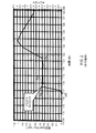
図2は、先行技術においてなされるような、イオン電流(時間単位あたりの単位面積あたりのイオン束)対時間のプロットを示している。図2において、点200は、ストライクステップの開始を表わしている。点200と点210との間の期間は、ストライクステップを表わしている。ステップ202は、プラズマの点火を反映している。実際、図2からわかるように、プラズマは、点204から既に安定化している。先行技術によるBKMは、ストライクステップ200の開始後に一定の期間を要求するので、ストライクステップは、その一定の期間が点210において満了するまで継続される。当業者ならば、点204と点210との間の期間が、基本的に無駄な時間を表わしていることが容易にわかり、これは、システムのスループットを低下させるとともに、安定化点の後の長時間に及ぶ導入プラズマの存在ゆえに基板及び/又はチャンバ部品を損傷させる可能性がある。
FIG. 2 shows a plot of ion current (ion flux per unit area per time unit) versus time, as is done in the prior art. In FIG. 2,
図3は、本発明の一実施形態にしたがった、イオン電流(時間単位あたりの単位面積あたりのイオン束)対時間のプロットを示している。図3において、点300は、ストライクステップの開始を表わしている。点302は、プラズマの点火を反映している。点火事象に続いて、プラズマは安定化し始める。点304において、プラズマは安定化される。プラズマの点火は、イオン束及び/又は電子温度及び/又は浮遊電位を監視することによって監視されえる。もし点302(プラズマの点火)と点304との間の時間内におけるプラズマ条件が満足のいくものである場合、エッチングプロセスは、点304から開始してよく、それによって、長時間に及ぶ無駄な時間(先行技術の図2の点204と210との間の時間など)を排除することができる。なお、もしプラズマの点火が検出されなかった(例えばステップ302がない)場合は、ストライクステップは失敗したと見なされる。このように、発明は、プラズマが成功裏に点火された且つ/又は安定化されたかどうかに関係なく所定のストライクステップ持続時間の満了時にエッチング工程が開始される先行技術に優る、大きな利点を提供する。
FIG. 3 shows a plot of ion current (ion flux per unit area per unit of time) versus time according to one embodiment of the present invention. In FIG. 3,
1つ又は2つ以上の実施形態では、エッチングの一例におけるプラズマ点火や安定化期間などについて、特性パラメータ測定結果(イオン束測定結果、電子温度測定結果、及び/又は浮遊電位測定結果など)が実験的に得られてよい。何枚かのテスト基板について、これらの特性パラメータが突き止められたら、その特性パラメータパターンは、ストライクステップが成功裏に完了されたかどうかを判定するために、のちのプロセス実行からのパラメータ読み取り値と照らして比較するために利用されてよい。 In one or more embodiments, characteristic parameter measurement results (such as ion flux measurement results, electron temperature measurement results, and / or floating potential measurement results) are experimentally tested for plasma ignition, stabilization period, etc. in an example of etching. May be obtained automatically. Once these characteristic parameters have been determined for a number of test boards, the characteristic parameter pattern is checked against parameter readings from subsequent process runs to determine if the strike step has been successfully completed. May be used for comparison.
入射又は反射のRF電力又はRFインピーダンスプローブを測定するなどの、先行技術によるパラメータ測定技術とは対照的に、発明によるCCEプローブをベースにしたストライクステップ検出技術は、高感度である。これは、発明の実施形態が、処理されている基板の近くにおいて、リアクタ壁に向かうイオン束を直接測定するプローブを使用するからである。したがって、プローブによって測定されるイオン束は、基板表面に到着する束に非常に密接に関係し、この測定を、本質的に絶対的な測定にする。したがって、検出システムは、エッチング工程への移行を始動させる前に、イオン束が安定している(例えば不当な振動、即ち不安定性がない)こと及び設定制御限界内であることを確認しえる。 In contrast to prior art parameter measurement techniques, such as measuring incident or reflected RF power or RF impedance probes, strike step detection techniques based on CCE probes according to the invention are highly sensitive. This is because embodiments of the invention use a probe that directly measures the ion flux towards the reactor wall near the substrate being processed. Thus, the ion flux measured by the probe is very closely related to the flux arriving at the substrate surface, making this measurement essentially an absolute measurement. Thus, the detection system can confirm that the ion flux is stable (eg, without undue vibration or instability) and within set control limits before initiating the transition to the etch process.
この直接的な測定手法は、より非直接的な測定である傾向がある且つストライクステップの検出について誤検出及び/又は検出漏れを発生しがちである且つ較正する又は絶対的にするのがより困難である先行技術による技術(上記のRF電力測定又はRFインピーダンスプローブ測定など)と異なる。 This direct measurement technique tends to be a more indirect measurement and is prone to false detections and / or omissions in the detection of strike steps and is more difficult to calibrate or make absolute Different from the prior art techniques (such as RF power measurement or RF impedance probe measurement above).
また、CCEプローブは、小さいものである傾向があり、プラズマ処理チャンバの周辺プラズマ対向構造と同一面になるように取り付けられ、チャンバのプラズマ対向部品と同じ材料で形成されるプラズマ対向プローブ表面を有することが可能であるゆえに、プラズマに対する摂動が最小である。更に、電流は、プローブヘッドのプラズマ対向表面上に形成されえる任意の付着を通じて容量結合されるので、発明によるCCEプローブベースのストライクステップ検出技術は、プラズマ対向プローブヘッド上のポリマ付着に反応しにくい。 CCE probes also tend to be small and have a plasma facing probe surface that is mounted to be flush with the plasma facing structure of the plasma processing chamber and is made of the same material as the plasma facing components of the chamber. The perturbation to the plasma is minimal. Furthermore, since the current is capacitively coupled through any attachment that can be formed on the plasma facing surface of the probe head, the CCE probe-based strike step detection technique according to the invention is less sensitive to polymer attachment on the plasma facing probe head. .
本発明は、幾つかの好ましい実施形態の観点から説明されているが、本発明の範囲内に入るものとして、代替形態、置換形態、及び均等物がある。また、本発明の方法及び装置を実現する多くの代替的手法があることも留意されるべきである。本明細書では、種々の例が提供されるが、これらの例は、例示的であって、発明に対して限定的であることを意図されない。 Although the invention has been described in terms of several preferred embodiments, there are alternatives, substitutions, and equivalents that fall within the scope of the invention. It should also be noted that there are many alternative ways of implementing the method and apparatus of the present invention. Various examples are provided herein, but these examples are illustrative and not intended to be limiting on the invention.
また、名称及び要約は、便宜のために本明細書に提供されており、特許請求の範囲の範囲を解釈するために用いられるべきでない。更に、要約は、極めて短縮された形で記載され、便宜のために本明細書に提供されており、したがって、特許請求の範囲に述べられた発明全体を解釈する又は制限するために用いられるべきでない。もし本明細書において「集合」という用語が用いられる場合は、このような用語は、ゼロ、1つ、又は2つ以上の要素を含む普通に理解される数学的意味を有することを意図される。また、以下の添付の特許請求の範囲は、本発明の真の趣旨及び範囲に含まれるものとしてこのようなあらゆる代替形態、置換形態、及び均等物を含むと解釈されることを意図される。 Also, names and abstracts are provided herein for convenience and should not be used to interpret the scope of the claims. Further, the abstract is described in a highly shortened form and is provided herein for convenience and therefore should be used to interpret or limit the entire invention as set forth in the claims. Not. If the term “set” is used herein, such term is intended to have a commonly understood mathematical meaning including zero, one, or two or more elements. . Also, it is intended that the following appended claims be construed to include all such alternatives, substitutions, and equivalents as included within the true spirit and scope of the invention.
「考察」は、「Methods for Automatically Characterizing a Plasma(プラズマを自動的に特性化するための方法)」と題され、2008年6月26日付けで米国特許局に出願された同時係属出願(出願番号61/075,948号)及び2009年6月2日付けで米国特許庁に出願された同時係属出願(出願番号第12/477,007号)にも見いだされ、引用によって本明細書に組み込まれる。 “Discussion” is entitled “Methods for Automatically Characterizing a Plasma” and is a co-pending application filed with the US Patent Office on June 26, 2008 (application) No. 61 / 075,948) and co-pending applications (Application No. 12 / 477,007) filed with the US Patent Office on June 2, 2009 and incorporated herein by reference. It is.
「プラズマを自動的に特性化するための方法の考察」 "Consideration of methods for automatically characterizing plasmas"
プラズマ処理の進歩は、半導体産業の成長を導いてきた。標準的な一電子製品のチップを供給するには、幾百又は幾千の基板(半導体ウエハなど)が処理されると考えられる。競争力を有するために、メーカは、最短の処理時間で基板を処理して高品質の半導体素子に仕上げられる必要がある。 Advances in plasma processing have led to the growth of the semiconductor industry. Hundreds or thousands of substrates (such as semiconductor wafers) are considered to be processed to supply a standard single-electronic product chip. In order to be competitive, manufacturers need to process substrates in the shortest processing time to finish high quality semiconductor devices.
通常、プラズマ処理中は、基板に悪影響を及ぼす可能性がある問題が発生しえる。処理されている基板の品質を変える可能性がある重要な要因は、1つには、プラズマ自体である。プラズマを解析するのに十分なデータを得るためには、各基板に関する処理データを収集するためのセンサが用いられてよい。収集されたデータは、問題の原因を突き止めるために解析されてよい。 In general, problems can occur during plasma processing that can adversely affect the substrate. One important factor that can change the quality of the substrate being processed is, in part, the plasma itself. In order to obtain sufficient data to analyze the plasma, sensors for collecting processing data for each substrate may be used. The collected data may be analyzed to determine the cause of the problem.
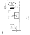
考察を進めるため、図4−Aは、プラズマシステムA−100の一部におけるデータ収集プローブの簡単な配線図を示している。プラズマシステムA−100は、プラズマA−106を発生させるためにリアクタチャンバA−104に容量結合される、パルス状RF周波発生器などの高周波(RF)源A−102を含んでよい。RF源A−102がオンにされると、外部コンデンサA−108にバイアス電圧がかけられ、これは、約26.2ナノファラッド(nF)でありえる。一例では、RF源A−102は、数ミリ秒(例えば約5ミリ秒)ごとに小さな電力バースト(例えば11.5メガヘルツ)を提供して外部コンデンサA−108を充電させてよい。RF源A−102がオフにされると、外部コンデンサA−108には、極性を持つバイアス電圧が残るので、プローブA−110は、バイアスをかけられてイオンを収集する。バイアス電圧が減衰するにつれて、図4−B1、図4−B2、及び図4−Cに示されるような曲線が描かれると考えられる。 For further discussion, FIG. 4-A shows a simplified wiring diagram of a data collection probe in a portion of plasma system A-100. Plasma system A-100 may include a radio frequency (RF) source A-102, such as a pulsed RF frequency generator, that is capacitively coupled to reactor chamber A-104 to generate plasma A-106. When the RF source A-102 is turned on, a bias voltage is applied to the external capacitor A-108, which can be approximately 26.2 nanofarads (nF). In one example, RF source A-102 may provide a small power burst (eg, 11.5 megahertz) every few milliseconds (eg, about 5 milliseconds) to charge external capacitor A-108. When the RF source A-102 is turned off, a bias voltage with polarity remains in the external capacitor A-108, so the probe A-110 is biased to collect ions. As the bias voltage decays, curves like those shown in FIGS. 4-B1, 4-B2, and 4-C may be drawn.
当業者ならば、プローブA−110が大抵は、リアクタチャンバA−104の壁を背にして位置決め可能な伝導性の平面を持つ電気プローブであることを承知している。プローブA−110は、したがって、リアクタチャンバA−104環境に直接曝される。プローブA−110によって収集された電流データ及び電圧データは、解析されてよい。レシピによっては、プローブA−110上に非伝導性の付着層A−116を付着させる可能性があるので、全てのプローブが、信頼できる測定結果を収集できるとは限らない。しかしながら、当業者ならば、PIF(平面イオン束)プローブが、測定の実施のために直流(DC)を引き込む必要がないその方式ゆえに、非伝導性の付着層にもかかわらずデータを収集可能であることを承知している。 Those skilled in the art are aware that probe A-110 is typically an electrical probe having a conductive plane that can be positioned against the wall of reactor chamber A-104. Probe A-110 is therefore directly exposed to the reactor chamber A-104 environment. The current data and voltage data collected by probe A-110 may be analyzed. Depending on the recipe, the non-conductive adhesion layer A-116 may be deposited on the probe A-110, so that not all probes can collect reliable measurement results. However, those skilled in the art can collect data in spite of a non-conductive adhesion layer because the PIF (planar ion flux) probe does not need to draw direct current (DC) to perform the measurement. I know there is.
プラズマシステムA−100内における電流信号及び電圧信号は、他のセンサによって測定される。例において、RF源A−102がオフに切り替えられると、電流及び電圧をそれぞれ測定するために、電流センサA−112及び高インピーダンス電圧センサA−114が用いられる。電流センサA−112及び電圧センサA−114から収集された測定データは、次いで、プロットされて電流グラフ及び電圧グラフに作成されえる。データは、手作業でプロットされてグラフに作成されてもよいし、又はソフトウェアプログラムに入力されてグラフに作成されてもよい。 Current and voltage signals within plasma system A-100 are measured by other sensors. In the example, when RF source A-102 is switched off, current sensor A-112 and high impedance voltage sensor A-114 are used to measure current and voltage, respectively. The measurement data collected from current sensor A-112 and voltage sensor A-114 can then be plotted to create current and voltage graphs. The data may be manually plotted and created into a graph, or may be input to a software program and created into a graph.
図4−B1は、RF充電サイクル後における電圧対時間のグラフを示している。データ点B1−202において、RF源A−102は、RF充電がなされた後にオフに切り替えられている(即ち、RFバースト)。この例では、データ点B1−202において、プローブA−110にかかる電圧は、約マイナス57ボルトである。プラズマシステムA−100が、休止状態(データ点B1−204とB1−206との間の区間)に戻るにつれて、電圧は、大抵は浮遊電圧電位に達する。この例では、浮遊電圧電位は、約マイナス57ボルトから約ゼロボルトに上昇する。しかしながら、浮遊電圧電位は、ゼロである必要はなく、マイナス又はプラスのバイアス電圧電位であってもよい。 FIG. 4-B1 shows a graph of voltage versus time after an RF charging cycle. At data point B1-202, RF source A-102 is switched off after the RF charge has been made (ie, RF burst). In this example, at data point B1-202, the voltage across probe A-110 is approximately minus 57 volts. As plasma system A-100 returns to a quiescent state (interval between data points B1-204 and B1-206), the voltage mostly reaches a floating voltage potential. In this example, the floating voltage potential rises from about minus 57 volts to about zero volts. However, the floating voltage potential need not be zero, and may be a negative or positive bias voltage potential.
同様に、図4−B2は、RF充電後における収集された電流データのグラフを示している。データ点B2−252において、RF源A−102は、RF充電がなされた後にオフに切り替えられている。減衰期間B2−254中に、外部コンデンサA−108における戻り電流は、放電されるであろう。一例では、満充電のときに(データ点B2−252)、電流は、約0.86mA/cm2である。しかしながら、電流は、完全に放電されたときに(データ点B2−256)、ゼロに戻っている。このグラフに基づくと、放電は、約75ミリ秒かかる。データ点B2−256からデータ点B2−258までの間、コンデンサは、放電された状態にとどまる。 Similarly, FIG. 4-B2 shows a graph of collected current data after RF charging. At data point B2-252, RF source A-102 is switched off after the RF charge is made. During the decay period B2-254, the return current in the external capacitor A-108 will be discharged. In one example, when fully charged (data point B2-252), the current is about 0.86 mA / cm 2 . However, the current is back to zero when fully discharged (data point B2-256). Based on this graph, the discharge takes about 75 milliseconds. Between data point B2-256 and data point B2-258, the capacitor remains discharged.
電流データ及び電圧データは、一定期間にわたって収集されるので、電流対電圧グラフは、時間で統合して時間変数を排除することによって作成されえる。換言すると、収集された電流データは、収集された電圧データに対応付けられてよい。図4−Cは、RFバースト間の一時間区間に及ぶ簡単な電流対電圧グラフを示している。データ点C−302において、RF源A−102は、RF充電がなされた後にオフに切り替えられている。 Since current data and voltage data are collected over a period of time, a current versus voltage graph can be created by integrating over time and eliminating time variables. In other words, the collected current data may be associated with the collected voltage data. FIG. 4-C shows a simple current versus voltage graph over a time interval between RF bursts. At data point C-302, RF source A-102 is switched off after the RF charge is made.
各RFバースト中に収集されたデータに対して非線形適合を適用することによって、プラズマA−106が特性化されてよい。換言すると、プラズマA−106を特性化しえるパラメータ(例えば、イオン飽和、イオン飽和の傾き、電子温度、浮遊電圧電位など)が決定されてよい。プラズマA−106は、収集されたデータによって特性化されてよいが、パラメータを計算するプロセスは、人による介在を必要とする単調な手作業のプロセスである。一例では、各RFバースト後(即ち、RF充電がなされ、次いでオフにされたとき)に収集されたデータを、ソフトウェア解析プログラムに取り込んでよい。ソフトウェア解析プログラムは、プラズマを特性化しえるパラメータを決定するために、非線形適合を実施してよい。プラズマを特性化することによって、技術者は、基板の低水準処理を最小限に抑えるためにどのようにレシピを調整すればよいかを決定できると考えられる。 Plasma A-106 may be characterized by applying a non-linear fit to the data collected during each RF burst. In other words, parameters that can characterize plasma A-106 (eg, ion saturation, slope of ion saturation, electron temperature, floating voltage potential, etc.) may be determined. Plasma A-106 may be characterized by the collected data, but the process of calculating the parameters is a tedious manual process that requires human intervention. In one example, data collected after each RF burst (ie, when RF charge is made and then turned off) may be captured in a software analysis program. The software analysis program may perform a non-linear fit to determine parameters that can characterize the plasma. By characterizing the plasma, it is believed that technicians can determine how to adjust the recipe to minimize low level processing of the substrate.
あいにく、各RFバーストについてデータを解析する先行技術の方法は、完了までに数秒の、又は数分もの時間を必要する可能性がある。解析されるべきRFバーストは、幾百万まではいかなくても通常幾千はあるので、レシピのためにプラズマを特性化するには、計算のために合計で幾時間も費やされると考えられる。ゆえに、先行技術の方法は、プロセス制御目的で時宜に即した関連データを提供するのに効果的な方法ではない。 Unfortunately, prior art methods of analyzing data for each RF burst can require several seconds or even minutes to complete. Since there are usually thousands of RF bursts to be analyzed, if not millions, it can be considered that a total of hours are spent calculating to characterize the plasma for the recipe. . Therefore, prior art methods are not effective methods for providing relevant data in a timely manner for process control purposes.
添付の図面に例示される幾つかの実施形態を参照にして、本発明が詳細に説明される。以下の説明では、本発明の完全な理解を可能にするために、多くの詳細が特定されている。しかしながら、当業者ならば明らかなように、本発明は、これらの一部又は全部の詳細を特定しなくても実施されえる。また、本発明が不必要に不明瞭にされないように、周知のプロセス工程及び/又は構造は詳細に説明されていない。 The present invention will now be described in detail with reference to a few embodiments illustrated in the accompanying drawings. In the following description, numerous details are set forth to provide a thorough understanding of the present invention. However, it will be apparent to those skilled in the art that the present invention may be practiced without identifying some or all of these details. In other instances, well known process steps and / or structures have not been described in detail in order not to unnecessarily obscure the present invention.
以下では、方法及び技術を含む、種々の実施形態が説明される。発明は、発明技術の実施形態を実施するためのコンピュータ可読命令を格納されたコンピュータ可読媒体を含む製造品も対象としえることを、念頭に置かれるべきである。コンピュータ可読媒体は、コンピュータ可読コードを格納するための、例えば半導体、磁気、光磁気、光、又はその他の形態のコンピュータ可読媒体を含みえる。更に、発明は、発明の実施形態を実施するための装置も対象としえる。このような装置は、発明の実施形態にかかわるタスクを実施するための、専用の及び/又はプログラム可能な回路を含みえる。このような装置の例は、適切にプログラムされたときの汎用コンピュータ及び/又は専用計算装置を含み、コンピュータ/計算装置と、発明の実施形態にかかわる種々のタスクに適応された専用の/プログラム可能な回路との組み合わせを含みえる。 In the following, various embodiments will be described, including methods and techniques. It should be borne in mind that the invention may also be directed to an article of manufacture that includes a computer readable medium having stored thereon computer readable instructions for implementing embodiments of the inventive technique. Computer-readable media may include, for example, semiconductor, magnetic, magneto-optical, optical, or other forms of computer-readable media for storing computer-readable code. Furthermore, the invention can also be directed to an apparatus for carrying out an embodiment of the invention. Such an apparatus may include dedicated and / or programmable circuitry for performing tasks according to embodiments of the invention. Examples of such devices include general purpose computers and / or dedicated computing devices when properly programmed, dedicated / programmable adapted to the various tasks involved in the computer / computing devices and embodiments of the invention. Combination with various circuits.
上記のように、プラズマに関するデータを収集するためにPIFプローブ法が用いられ、リアクタチャンバ環境内に位置決めされてよい。センサ(例えばPIFプローブ)から収集されたデータは、リアクタチャンバ内のプラズマを特性化するために用いられてよい。また、センサは、図4−Aに示されるように収集表面を用いるので、チャンバの表面に関するデータも決定されえる。先行技術では、PSDによって収集されたデータが、解析に利用可能な即座のデータ源を提供する。あいにく、収集されえるデータの甚大な量が、時宜に即したデータの解析を困難にしている。幾千の、又は幾百万ものデータ点が収集されえるので、プラズマを正確に特性化するために関連区間を測定する作業は、とりわけデータが大抵は手作業で解析されるゆえに、気の遠くなる作業になるであろう。結果的に、収集されたデータは、時宜に即したプラズマの特性化をプラズマ処理システムに提供するのに有用ではなかった。 As described above, the PIF probe method may be used to collect data about the plasma and positioned within the reactor chamber environment. Data collected from a sensor (eg, a PIF probe) may be used to characterize the plasma in the reactor chamber. Also, because the sensor uses a collection surface as shown in FIG. 4-A, data regarding the surface of the chamber can also be determined. In the prior art, the data collected by PSD provides an immediate source of data available for analysis. Unfortunately, the vast amount of data that can be collected makes it difficult to analyze the data in a timely manner. Since thousands or millions of data points can be collected, the task of measuring the relevant intervals to accurately characterize the plasma is not easy, especially because the data is usually analyzed manually. Will be the work. As a result, the collected data has not been useful in providing timely plasma characterization to plasma processing systems.
しかしながら、もし、プラズマの特性化に必要とされる関連のデータ点が、収集されえる幾千/幾百万のデータ点から特定されるならば、プラズマの特性化に必要とされる時間は、大幅に短縮されるであろう。発明の実施形態にしたがって、比較的短期間でプラズマを自動的に特性化するための方法が提供される。本明細書において説明される発明の実施形態は、プラズマを特性化するための解析を必要としえるデータ点を減らすために関連性範囲を特定するためのアルゴリズムを提供する。本明細書において論じられるように、関連性範囲は、各RFバースト間に収集されえる幾千又は幾百万のデータ点のなかの、より小さいデータ点の集合を言う。発明の実施形態は、更に、プラズマを特性化するための値を計算する数学モデルに適用されえるシード値を推定することも提供する。関連性範囲に対して曲線適合を実施することによって、プラズマを特性化するために利用されえるパラメータが計算されえる。 However, if the relevant data points required for plasma characterization are identified from the thousands / millions of data points that can be collected, the time required for plasma characterization is Will be greatly shortened. In accordance with an embodiment of the invention, a method is provided for automatically characterizing a plasma in a relatively short period of time. The embodiments of the invention described herein provide an algorithm for identifying relevance ranges to reduce data points that may require analysis to characterize the plasma. As discussed herein, a relevance range refers to a smaller set of data points among thousands or millions of data points that can be collected during each RF burst. Embodiments of the invention also provide for estimating a seed value that can be applied to a mathematical model that calculates a value for characterizing the plasma. By performing a curve fit to the relevance range, parameters that can be used to characterize the plasma can be calculated.
本発明の特徴及び利点は、以下の図面及び議論を参照にして更に良く理解されるであろう。 The features and advantages of the present invention may be better understood with reference to the drawings and discussions that follow.
図4−Dは、発明の一実施形態における、基板処理中にプラズマを自動的に特性化するための工程を説明した簡単なフローチャートを示している。基板処理中にRF充電が提供された状況を考える。 FIG. 4-D shows a simple flowchart describing steps for automatically characterizing a plasma during substrate processing in one embodiment of the invention. Consider a situation where RF charging was provided during substrate processing.
第1の工程D−402では、電流データ及び電圧データが収集される。一例では、RF源がオンにされた後に、RF充電(パルス)が提供される。RF充電がオフにされた後は、リアクタチャンバのチャンバ壁に取り付け可能な平面イオン束プローブなどのプローブでデータを収集するために、電流センサ及び電圧センサが用いられてよい。上記のように、センサによって収集されえるデータ点の数は、幾千又は幾百万に及ぶであろう。一部のケースでは、各RFバースト間において幾千から幾万のデータ点が収集されることがあり、これは、先行技術によるリアルタイムに近い解析をほぼ不可能にする。 In the first step D-402, current data and voltage data are collected. In one example, RF charging (pulse) is provided after the RF source is turned on. After RF charging is turned off, current and voltage sensors may be used to collect data with a probe such as a planar ion flux probe that can be attached to the chamber wall of the reactor chamber. As noted above, the number of data points that can be collected by a sensor may range in the thousands or millions. In some cases, thousands to tens of thousands of data points may be collected between each RF burst, making near real time analysis according to the prior art nearly impossible.
先行技術では、半導体基板処理中に収集される測定データを解析するために、数時間の時間が充てられることがある。ここで、発明の一態様では、発明者らは、プラズマの特性化のために各RFバースト間における測定データを解析する必要はないことに気付いた。その代わりに、もし、データ集合の関連性範囲に対して曲線適合が適用されるならば、プラズマの特性化に利用されえるパラメータが決定されるであろう。 In the prior art, several hours may be devoted to analyzing measurement data collected during semiconductor substrate processing. Here, in one aspect of the invention, the inventors have realized that it is not necessary to analyze the measurement data between each RF burst for plasma characterization. Instead, if a curve fit is applied to the relevance range of the data set, the parameters that can be used to characterize the plasma will be determined.
次の工程D−404では、関連性範囲が決定される。上記のように、関連性範囲は、各RFバースト間に収集されたデータ集合のなかの小集合を言う。先行技術では、データは手作業で解析されているので、収集されたデータの甚大な量は、関連性範囲の計算を困難な作業にする。多くの場合、関連性範囲は、視覚的に推定されえる。関連性範囲を特定するにあたっては、データ集合のなかの小集合から、存在しえるノイズが実質的に排除されてよい。一例では、複雑な基板処理中に、プローブ上にポリマが蓄積され、収集されたデータの一部を歪曲させることがある。例えば、影響を受けるデータの一部は、コンデンサが完全に放電された時点で収集されえるデータである傾向がある。関連性範囲を特定するにあたっては、ポリマの蓄積に関連したデータが、解析から取り除かれてよい。換言すると、関連性範囲の決定は、プラズマの特性化が不規則ノイズに見舞われることなく行われることを可能にしえる。一例として、関連性範囲がどのように決定されえるかに関しては、下記の図4−Eの考察において論じられる。 In the next step D-404, the relevance range is determined. As described above, the relevance range refers to a small set of data sets collected during each RF burst. In the prior art, the data is analyzed manually, so the large amount of data collected makes the calculation of the relevance range difficult. In many cases, the relevance range can be estimated visually. In specifying the relevance range, noise that may exist may be substantially excluded from a small set in the data set. In one example, during complex substrate processing, polymers can accumulate on the probe and distort some of the collected data. For example, some of the affected data tends to be data that can be collected when the capacitor is fully discharged. In identifying the relevance range, data related to polymer accumulation may be removed from the analysis. In other words, determining the relevance range may allow the plasma characterization to be performed without suffering from random noise. As an example, how the relevance range can be determined is discussed in the discussion of FIG. 4-E below.
関連性範囲を特定することに加えて、次の工程D−406では、シード値も決定されてよい。本明細書において論じられるように、シード値は、傾き、電子温度、イオン飽和値、浮遊電圧電位などの推定値を言う。例えばシード値がどのように推定されえるかに関しては、図4−Eの考察において提供される。 In addition to identifying the relevance range, in the next step D-406, a seed value may also be determined. As discussed herein, the seed value refers to an estimate such as slope, electron temperature, ion saturation value, floating voltage potential. For example, how the seed value can be estimated is provided in the discussion of FIG.
関連性範囲及びシード値は、曲線適合を実施するために用いられる。曲線適合は、次のRFバースト前に実施される必要があるので、関連性範囲及び/又はシード値を決定するために用いられる方法は、最小限のオーバーヘッドで最終適合値に近い値を生成することによって、急速な収束を達成するために必要とされえる曲線適合の反復回数を減らす必要がある。 The relevance range and seed value are used to perform curve fitting. Since curve fitting needs to be performed before the next RF burst, the method used to determine the relevance range and / or seed value produces a value close to the final fitting value with minimal overhead. Thus, it is necessary to reduce the number of curve fitting iterations that may be required to achieve rapid convergence.
関連性範囲及びシード値によって、次の工程D−408では、非線形適合(例えば曲線適合)が実施されることによって、高価な高性能のコンピュータを必要とすることなく短期間でプラズマが特性化されることを可能にしてよい。先行技術と異なり、この方法は、処理のために数分、又は数時間もの時間を必要とする代わりに、一RFバーストに起因する減衰区間からの結果がおよそ20ミリ秒内に特性化されることを可能にする。リアルタイムに近い解析能力によって、この方法は、自動制御システムの一部として適用されて、プラズマ処理中に技術者に関連データを提供しえる。 Depending on the relevance range and seed value, in the next step D-408, non-linear fitting (eg curve fitting) is performed to characterize the plasma in a short time without the need for expensive high performance computers. You may be able to Unlike the prior art, this method is characterized in that the result from the decay interval due to one RF burst is approximately 20 milliseconds instead of requiring minutes or even hours to process. Make it possible. With near real-time analysis capabilities, this method can be applied as part of an automated control system to provide relevant data to technicians during plasma processing.
図4−Eは、発明の一実施形態における、関連性範囲及びシード値を決定するための簡単なアルゴリズムを示している。図4−Eは、図4−F1、図4−F2、図4−F3、及び図4−F4との関連で論じられる。 FIG. 4-E illustrates a simple algorithm for determining the relevance range and seed value in one embodiment of the invention. FIG. 4-E is discussed in the context of FIG. 4-F1, FIG. 4-F2, FIG. 4-F3, and FIG. 4-F4.
第1の工程E−502では、各RFバースト中に収集されたデータが、自動的にプロットされる。一例では、電流センサによって収集される電流データがプロットされ、図4−F1に示されるような電流対時間グラフF1−600に作成される。別の例では、収集された電圧データがプロットされ、図4−F2に示されるような電圧対時間グラフF2−650に作成されてよい。データは、先行技術の場合と同様のグラフを生じえるが、先行技術と異なり、収集されたデータは、人による介在を必要とすることなく自動的に解析プログラムに取り込まれる。或いは、収集された測定データは、プロットされる必要がなく、その代わりに、解析プログラムに直接取り込まれてよい。その代わりに、グラフは、アルゴリズムを説明するための視覚的な例として提供される。 In the first step E-502, the data collected during each RF burst is automatically plotted. In one example, current data collected by the current sensor is plotted and generated in a current versus time graph F1-600 as shown in FIG. 4-F1. In another example, collected voltage data may be plotted and generated in a voltage versus time graph F2-650 as shown in FIG. 4-F2. The data can produce a graph similar to that of the prior art, but unlike the prior art, the collected data is automatically imported into the analysis program without the need for human intervention. Alternatively, the collected measurement data does not need to be plotted, but instead may be taken directly into the analysis program. Instead, the graph is provided as a visual example to illustrate the algorithm.
先行技術と異なり、プラズマを特性化するためにデータ集合全体が解析されるのではなく、その代わりに、関連性範囲が決定される。関連性範囲を決定するために、次の工程E−504では、先ず、パーセント減衰点が決定されてよい。本明細書において論じられるように、パーセント減衰点は、初めの値がその一定のパーセントまで減衰したところのデータ点を言う。一実施形態では、パーセント減衰点は、解析されるべきデータ区間の終わりを表わしてよい。一例において、RF源がオフに切り換えられたとき、電流値は、約0.86mA/cm2である。値は、図4−F1のグラフF1−600上のデータ点F1−602によって表わされる。もしパーセント減衰点が、初めの値の10パーセントに設定されるならば、パーセント減衰点は、データ点F1−604にあり、約0.086mA/cm2である。換言すると、パーセント減衰点は、RF源がオフに切り換えられシステムが平衡状態に戻っていくときの電荷の値である初めの値の所定のパーセントをとることによって決定されてよい。一実施形態では、パーセントは、経験的に決定される。一実施形態では、データ区間の終わりを決定するためにパーセント減衰点を用いる代わりに、各RFバーストについて収集されたデータの一次微分のピークが計算されてよい。 Unlike the prior art, the entire data set is not analyzed to characterize the plasma, but instead the relevance range is determined. To determine the relevance range, in the next step E-504, a percent decay point may first be determined. As discussed herein, the percent decay point refers to the data point where the initial value decays to that constant percentage. In one embodiment, the percent decay point may represent the end of the data interval to be analyzed. In one example, when the RF source is switched off, the current value is about 0.86 mA / cm 2 . The value is represented by data point F1-602 on graph F1-600 in FIG. If the percent decay point is set to 10 percent of the original value, the percent decay point is at data point F1-604 and is about 0.086 mA / cm 2 . In other words, the percent decay point may be determined by taking a predetermined percentage of the initial value that is the value of the charge when the RF source is switched off and the system returns to equilibrium. In one embodiment, the percentage is determined empirically. In one embodiment, instead of using a percent decay point to determine the end of the data interval, a peak of the first derivative of the data collected for each RF burst may be calculated.
次の工程E−506では、アルゴリズムは、初めの値と第2の減衰点との間のデータ小集合であるイオン飽和区間を決定してよい。本明細書において論じられるイオン飽和区間は、プローブへの電子束が無視できるようにプローブ電位が浮遊電位に対して十分に負であるような電流電圧(IV)曲線の領域を言う。この領域では、プローブへの電流は、電位の負の度合いが増すにつれて緩やかに線形に増加する。また、イオン飽和区間は、プローブがシステム内における利用可能イオンを全て収集できるようにバイアス電圧が浮遊電位に対して十分に負であるような領域である。換言すると、収集される電流は、バイアス電圧が十分高く上昇されるにつれて「飽和」する。また、本明細書において論じられるように、「利用可能イオン」は、「シース境界」に衝突するイオン束を言い、これは、バイアス電圧が更に増加されるにつれて拡大するであろう。 In a next step E-506, the algorithm may determine an ion saturation interval that is a small set of data between the initial value and the second decay point. The ion saturation interval discussed herein refers to the region of the current voltage (IV) curve where the probe potential is sufficiently negative with respect to the floating potential so that the electron flux to the probe is negligible. In this region, the current to the probe increases slowly and linearly as the negative degree of potential increases. Also, the ion saturation interval is a region where the bias voltage is sufficiently negative with respect to the floating potential so that the probe can collect all available ions in the system. In other words, the collected current “saturates” as the bias voltage is raised high enough. Also, as discussed herein, “available ions” refers to ion fluxes that impinge on “sheath boundaries,” which will expand as the bias voltage is further increased.
換言すると、イオン飽和区間は、図4−F1のデータ点F1−602からF1−606までの区間である。一実施形態では、第2の減衰点は、初めの値(即ち、データ点F1−602)のパーセントをとることによって決定されてよい。一例において、もし第2の減衰点が、初めの値の約95パーセントであるならば、第2の減衰点は、約0.81mA/cm2(即ち、データ点F1−606)である。したがって、イオン飽和区間は、初めの値(データ点F1−602)から第2の減衰点(データ点F1−606)までである。なお、第2の減衰点は、初めの値(データ点F1−602)とパーセント減衰点(データ点F1−604)との間であることがわかる。パーセント減衰点と同様に、第2の減衰点もまた、一実施形態では所定の閾値に基づいてよい。一実施形態では、パーセントは、経験的に決定される。 In other words, the ion saturation interval is an interval from data points F1-602 to F1-606 in FIG. In one embodiment, the second decay point may be determined by taking a percentage of the initial value (ie, data point F1-602). In one example, if the second decay point is about 95 percent of the initial value, the second decay point is about 0.81 mA / cm 2 (ie, data point F1-606). Accordingly, the ion saturation interval is from the initial value (data point F1-602) to the second attenuation point (data point F1-606). Note that the second decay point is between the initial value (data point F1-602) and the percent decay point (data point F1-604). Similar to the percent decay point, the second decay point may also be based on a predetermined threshold in one embodiment. In one embodiment, the percentage is determined empirically.
イオン飽和区間が決定されたら、次の工程E−508では、傾き(s)及びイオン飽和(i0)が推定されてよい。上記のように、傾き(s)及びイオン飽和(i0)は、プラズマを特性化するパラメータを決定するために数学モデル(下記の式2)に適用されえる4つのシード値のうちの2つである。一例では、傾き(s)は、線形回帰を実施することによって決定されてよい。別の実施形態では、アルゴリズムは、データ点F1−602とF1−606との間のデータ値の平均をとることによってイオン飽和(i0)も決定してよい。
Once the ion saturation interval is determined, in the next step E-508, the slope (s) and ion saturation (i 0 ) may be estimated. As noted above, slope (s) and ion saturation (i 0 ) are two of four seed values that can be applied to a mathematical model (
次の工程E−510では、アルゴリズムは、二次微分が符号を変える点である変曲点を決定してよい。一実施形態では、変曲点は、パーセント減衰点と第2の減衰点との間の電流値の一次微分の最小値を特定することによって計算されてよい。説明のため、図4−F3は、電流信号F3−660のパーセント減衰点(F3−664)と初めの点(F3−662)との間の値の一次微分を示している。変曲点は、一次微分(F3−670)の最小データ点であり、(データ点F3−666によって示されるように)−0.012mA/cm2の値と226の指標値とを有する。変曲値を決定するために、指標値は、電流信号プロットF3−660に対してマッピングされている。この例において、一次微分の指標値が、電流信号F3−660に対してマッピングされているとき、変曲値は、データ点F3−668によって示されるように、0.4714mA/cm2である。 In a next step E-510, the algorithm may determine an inflection point where the second derivative changes sign. In one embodiment, the inflection point may be calculated by identifying the minimum value of the first derivative of the current value between the percent decay point and the second decay point. For purposes of illustration, FIG. 4-F3 shows the first derivative of the value between the percent decay point (F3-664) and the first point (F3-662) of the current signal F3-660. The inflection point is the minimum data point of the first derivative (F3-670) and has a value of −0.012 mA / cm 2 and an index value of 226 (as indicated by data point F3-666). In order to determine the inflection value, the index value is mapped to the current signal plot F3-660. In this example, the index value of the first derivative is, when it is mapped to current signal F3-660, Henkyokuchi, as indicated by the data points F3-668, a 0.4714mA / cm 2.
一実施形態では、関連性範囲は、初めの値と変曲点との間の範囲として定義される。その追加として又は代わりとして、変曲点を計算する代わりに(例えば35パーセントの)パーセント減衰閾値が設定されてよい。一例において、経験的に決定されえる35パーセントのパーセント減衰点を使用すると、関連性範囲は、図4−F1の点F1−602とF1−604との間に入るであろう。

変曲点を特定されたら、次の工程E−512では、電子温度が推定されてよい。電子温度は、上記の式1を用いて推定されてよい。電子温度を計算するために用いられる電流データ及び電圧データは、プローブが引き込む電流が大抵はイオン飽和電流よりも少ないときである推移区間内にある。一実施形態では、電流データ及び電圧データが測定される時刻は、変曲点に対応していてよい。或いは、電流電圧(I−V)曲線の変曲点が用いられてもよい。電子温度は、電流電圧曲線上の変曲点に対応する時刻における、一RFバーストについて収集されたデータの一次微分(パーセント減衰点を計算するにあたって決定される)の率であるので、その数字を生成するために必要とされえる計算のオーバーヘッドは、最小限である。
Once the inflection point is identified, in the next step E-512, the electron temperature may be estimated. The electron temperature may be estimated using
次の工程E−514では、アルゴリズムは、浮遊電圧電位を決定してよい。浮遊電圧電位は、収集された電圧データに基づいて決定されるので、浮遊電圧電位は、工程E1−504〜E−512において計算されるような値を最初に決定する必要なく決定されえる。当業者ならば、浮遊電圧電位が、外部コンデンサが完全に放電された後にプローブが浮遊する電位であることを承知している。通常、浮遊電圧電位は、次のRFバーストの直前に生じる信号を見ることによって決定されてよい。しかしながら、ポリマの蓄積が歪みを引き起こす可能性ゆえに、誤ったデータ(即ち、ノイズ)が収集されることがあり、したがって、浮遊電圧電位は、収集期間の終わり頃に収集される電圧値を平均化することによって計算されてよい。一実施形態では、浮遊電圧電位は、図4−F2に示されるように、データ点F2−652(電圧がその浮遊電位に最初に到達するデータ点)からデータ点F2−654(次のRFバーストの直前のデータ点)にかけて計算されてよい。別の実施形態では、浮遊電圧電位は、図4−F2に示されるようにデータ点F2−652とF2−654との間に位置する窓F2−656内の電圧値に基づいてよい。一実施形態では、窓F2−656は、先のパルスが99パーセントを超えて減衰する前に始まって次のパルスが始まる前に終わる限り、任意のサイズであってよい。一実施形態では、浮遊電圧電位は、標準偏差(誤差)の小さい平均値を提供する窓から決定されてよい。 In the next step E-514, the algorithm may determine a floating voltage potential. Since the floating voltage potential is determined based on the collected voltage data, the floating voltage potential can be determined without having to first determine values as calculated in steps E1-504 through E-512. One skilled in the art knows that the floating voltage potential is the potential at which the probe floats after the external capacitor is completely discharged. Usually, the floating voltage potential may be determined by looking at the signal that occurs just before the next RF burst. However, erroneous data (ie, noise) may be collected because polymer accumulation can cause distortion, so the stray voltage potential averages the voltage value collected around the end of the collection period. May be calculated by In one embodiment, the floating voltage potential is derived from data point F2-652 (the data point at which the voltage first reaches the floating potential) to data point F2-654 (next RF burst, as shown in FIG. 4-F2. May be calculated over the data point immediately before). In another embodiment, the floating voltage potential may be based on a voltage value in a window F2-656 located between data points F2-652 and F2-654 as shown in FIG. 4-F2. In one embodiment, window F2-656 may be of any size as long as it begins before the previous pulse decays by more than 99 percent and ends before the next pulse begins. In one embodiment, the stray voltage potential may be determined from a window that provides an average value with a small standard deviation (error).
以上からわかるように、関連性範囲及びシード値を決定するための方法は、電流、電圧、及び/又は電流電圧(I−V)曲線に生じえる異常を打ち消す。一例では、RFバーストの終わりにポリマの蓄積が発生しえる。しかしながら、上記のアルゴリズムを適用することによって、関連性範囲及びシード値は、処理中に発生しえる予想外のアーチファクトに影響されなくなる。 As can be seen, the method for determining the relevance range and seed value counteracts anomalies that may occur in current, voltage, and / or current-voltage (IV) curves. In one example, polymer accumulation may occur at the end of the RF burst. However, by applying the above algorithm, the relevance range and seed value are not affected by unexpected artifacts that may occur during processing.
関連性範囲が決定されシード値が計算されると、次の工程E−516では、図4−F4のグラフF4−680を作成するために、電流値が電圧値に対してプロットされ曲線適合が適用されてよい。一例では、曲線適合を実施するために、レベンバーグ・マーカード(Levenberg-Marquardt)アルゴリズムが適用されてよい。曲線適合グラフを作成すること、及び下記の式2のような数学モデルにシード値を適用することによって、プラズマを特性化するために利用されえる4つのパラメータが決定されえる。
本発明の1つ又は複数の実施形態からわかるように、プラズマ処理中にプラズマを特性化するための自動化された方法が提供される。関連性範囲及びシード値の集合を決定することによって、一RFバースト後に大抵収集される幾千又は幾百万のデータ点を処理する必要なくプラズマの特性化が生じえる。自動化されたこの方法は、手作業によるこれまでの単調なプロセスを、迅速に且つ効率良く実施されえる自動的な作業に転換する。データ解析を数分(又は数時間)から数ミリ秒に大幅に短縮されたことによって、プラズマ特性化は、製造プロセス後の代わりにプラズマ処理中に実施されえる。したがって、関連性データは、現時点のプラズマ環境を明らかにすることによって、レシピ及び/又はツールの調整を行うこと並びに廃棄を最小限に抑えることを可能にしえる。 As can be seen from one or more embodiments of the present invention, an automated method is provided for characterizing a plasma during plasma processing. By determining the set of relevance ranges and seed values, plasma characterization can occur without having to process thousands or millions of data points that are mostly collected after one RF burst. This automated method transforms the traditional tedious process of manual labor into automatic work that can be performed quickly and efficiently. By significantly reducing data analysis from minutes (or hours) to milliseconds, plasma characterization can be performed during plasma processing instead of after the manufacturing process. Thus, the relevance data may allow recipe and / or tool adjustments to be made and disposal to be minimized by revealing the current plasma environment.
本発明は、幾つかの好ましい実施形態の観点から説明されているが、本発明の範囲内に入るものとして、代替形態、置換形態、及び均等物がある。また、本発明の方法及び装置を実現する多くの代替的手法があることも留意されるべきである。本明細書では、種々の例が提供されるが、これらの例は、例示的であって、発明に対して限定的であることを意図されない。 Although the invention has been described in terms of several preferred embodiments, there are alternatives, substitutions, and equivalents that fall within the scope of the invention. It should also be noted that there are many alternative ways of implementing the method and apparatus of the present invention. Various examples are provided herein, but these examples are illustrative and not intended to be limiting on the invention.
また、名称及び要約は、便宜のために本明細書に提供されており、特許請求の範囲の範囲を解釈するために用いられるべきでない。更に、要約は、極めて短縮された形で記載され、便宜のために本明細書に提供されており、したがって、特許請求の範囲に述べられた発明全体を解釈する又は制限するために用いられるべきでない。もし本明細書において、「集合」という用語が用いられる場合は、このような用語は、ゼロ、1つ、又は2つ以上の要素を含む普通に理解される数学的意味を有することを意図される。また、以下の添付の特許請求の範囲は、本発明の真の趣旨及び範囲に含まれるものとしてこのようなあらゆる代替形態、置換形態、及び均等物を含むと解釈されることを意図される。 Also, names and abstracts are provided herein for convenience and should not be used to interpret the scope of the claims. Further, the abstract is described in a highly shortened form and is provided herein for convenience and therefore should be used to interpret or limit the entire invention as set forth in the claims. Not. If the term “set” is used herein, such terms are intended to have a commonly understood mathematical meaning including zero, one, or more than one element. The Also, it is intended that the following appended claims be construed to include all such alternatives, substitutions, and equivalents as included within the true spirit and scope of the invention.
Claims (20)
前記処理チャンバ内においてストライクステップを実行してプラズマを発生させることであって、前記ストライクステップは、
前記処理チャンバ内において、前記ストライクステップの後に行われるエッチングステップにおけるガス圧よりも高いガス圧を印加することと、
前記処理チャンバ内において、前記エッチングステップにおける高周波電力よりも低い高周波(RF)電力を維持することと、
を含む、ことと、
前記ストライクステップ中に、前記処理チャンバの表面上にあるプローブヘッドを利用して特性パラメータ測定結果の集合を収集することと、
前記特性パラメータ測定結果の集合を所定の範囲と照らして比較することと、
を備え、
前記特性パラメータ測定結果の集合が前記所定の範囲内である場合は、前記安定化プラズマが存在するものであり、
前記プローブヘッドを利用して特性パラメータ測定結果の集合を収集することは、
前記プローブヘッドで電流値と電圧値の時間変化を測定することと、
前記測定された電流値の時間変化において、初めの電流値と前記時間変化の変曲点との間の範囲、又は、前記始めの電流値と予め定められたパーセントにおけるパーセント減衰閾値との間の範囲を、関連性範囲として決定することと、
前記測定された電流値と電圧値の間の電流−電圧特性を前記関連性範囲において曲線適合することによって、前記特性パラメータ測定結果の集合を決定することと、を含む、方法。 A method for identifying a stabilized plasma in a processing chamber of a plasma processing system, comprising:
Performing a strike step in the processing chamber to generate plasma, wherein the strike step comprises:
Applying a gas pressure higher than the gas pressure in the etching step performed after the strike step in the processing chamber;
Maintaining a radio frequency (RF) power in the processing chamber that is lower than the radio frequency power in the etching step ;
Including, and
And that during said strike step, collecting a set of utilizing a probe head characteristic parameter measurement results on the surface of the processing chamber,
Comparing the set of characteristic parameter measurement results against a predetermined range;
With
When the set of characteristic parameter measurement results is within the predetermined range, the stabilized plasma is present ,
Collecting a set of characteristic parameter measurement results using the probe head,
Measuring temporal changes in current value and voltage value with the probe head;
In the time variation of the measured current value, the range between the initial current value and the inflection point of the time variation, or between the initial current value and a percent decay threshold in a predetermined percentage. Determining the scope as the scope of relevance;
Determining a set of characteristic parameter measurement results by curve fitting a current-voltage characteristic between the measured current value and voltage value in the relevance range .
前記プローブヘッドは、容量結合静電(CCE)プローブである、方法。 The method of claim 1, comprising:
The method, wherein the probe head is a capacitively coupled electrostatic (CCE) probe.
前記プローブヘッドのプラズマ対向表面は、前記処理チャンバのその他のプラズマ対向部品と同じ材料で作成される、方法。 The method of claim 2, comprising:
The plasma facing surface of the probe head is made of the same material as the other plasma facing components of the processing chamber.
前記特性パラメータ測定結果の集合は、イオン束測定結果の集合である、方法。 The method of claim 1, comprising:
The set of characteristic parameter measurement results is a set of ion flux measurement results.
前記特性パラメータ測定結果の集合は、電子温度測定結果の集合である、方法。 The method of claim 1, comprising:
The set of characteristic parameter measurement results is a set of electron temperature measurement results.
前記特性パラメータ測定結果の集合は、浮遊電位測定結果の集合である、方法。 The method of claim 1, comprising:
The set of characteristic parameter measurement results is a set of floating potential measurement results.
前記特性パラメータ測定結果の集合が前記所定の範囲内でない場合は、前記プラズマは安定化されておらず、修正措置がとられる、方法。 The method of claim 1, comprising:
If the set of characteristic parameter measurement results is not within the predetermined range, the plasma is not stabilized and corrective action is taken.
前記処理チャンバ内において下部電極上に位置決めされる基板と、
前記処理チャンバ内において、前記ストライクステップの後に行われるエッチングステップにおけるRF電力よりも低いRF電力を前記ストライクステップで印加する高周波(RF)電力源と、
前記RF電力と相互作用することによってプラズマを発生させるガスを前記処理チャンバ内に供給するガス供給システムと、
前記処理チャンバ内において、前記エッチングステップにおけるガス圧よりも高いガス圧を前記ストライクステップで印加する圧力モジュールと、
プラズマ対向センサを含み、前記処理チャンバの表面上に配され、少なくとも、前記ストライクステップ中に特性パラメータ測定結果の集合を収集するように構成されたプローブ構成と、
前記特性パラメータ測定結果の集合を所定の範囲と照らして比較するように構成される検出モジュールと、
を備え、
前記特性パラメータ測定結果の集合が前記所定の範囲内である場合は、前記安定化プラズマが存在するものであり、
前記プローブ構成は、
前記プラズマ対向センサで電流値と電圧値の時間変化を測定し、
前記測定された電流値の時間変化において、初めの電流値と前記時間変化の変曲点との間の範囲、又は、前記始めの電流値と予め定められたパーセントにおけるパーセント減衰閾値との間の範囲を、関連性範囲として決定し、
前記測定された電流値と電圧値の間の電流−電圧特性を前記関連性範囲において曲線適合することによって、前記特性パラメータ測定結果の集合を決定する、構成。 A configuration for identifying a stabilized plasma in a processing chamber of a plasma processing system when performing a strike step to generate plasma ,
A substrate positioned on the lower electrode in the processing chamber;
A radio frequency (RF) power source that applies RF power in the strike step that is lower than RF power in an etching step performed after the strike step in the processing chamber;
A gas supply system for supplying a gas into the processing chamber that generates plasma by interacting with the RF power;
A pressure module that applies a gas pressure higher than the gas pressure in the etching step in the strike step in the processing chamber;
A probe arrangement including a plasma facing sensor, disposed on a surface of the processing chamber and configured to collect at least a collection of characteristic parameter measurement results during the strike step;
A detection module configured to compare the set of characteristic parameter measurement results against a predetermined range;
With
When the set of characteristic parameter measurement results is within the predetermined range, the stabilized plasma is present ,
The probe configuration is:
Measure the time change of current value and voltage value with the plasma facing sensor,
In the time variation of the measured current value, the range between the initial current value and the inflection point of the time variation, or between the initial current value and a percent decay threshold in a predetermined percentage. Determine the scope as the relevance scope,
An arrangement for determining the set of characteristic parameter measurement results by curve fitting a current-voltage characteristic between the measured current value and voltage value in the relevance range .
前記プラズマ対向センサは、容量結合静電(CCE)プローブヘッドである、構成。 The configuration according to claim 8,
The plasma facing sensor is a capacitively coupled electrostatic (CCE) probe head.
前記プラズマ対向センサのプラズマ対向表面は、前記処理チャンバのその他のプラズマ対向部品と同じ材料で作成される、構成。 The configuration according to claim 9,
The plasma facing surface of the plasma facing sensor is made of the same material as the other plasma facing parts of the processing chamber.
前記特性パラメータ測定結果の集合は、イオン束測定結果の集合である、構成。 The configuration according to claim 8,
The set of characteristic parameter measurement results is a set of ion flux measurement results.
前記特性パラメータ測定結果の集合は、電子温度測定結果の集合である、構成。 The configuration according to claim 8,
The set of characteristic parameter measurement results is a set of electron temperature measurement results.
前記特性パラメータ測定結果の集合は、浮遊電位測定結果の集合である、構成。 The configuration according to claim 8,
The set of characteristic parameter measurement results is a set of floating potential measurement results.
前記検出モジュールは、ソフトウェアアルゴリズムである、構成。 The configuration according to claim 8,
The detection module is a software algorithm.
もし前記検出モジュールが、前記安定化プラズマを決定することができない場合は、修正措置がとられる、構成。 The configuration according to claim 8,
If the detection module is unable to determine the stabilized plasma, corrective action is taken.
前記処理チャンバ内においてストライクステップを実行してプラズマを発生させるためのコードであって、
前記処理チャンバ内において、前記ストライクステップの後に行われるエッチングステップにおけるガス圧よりも高いガス圧を印加させるためのコードと、
前記処理チャンバ内において、前記エッチングステップにおける高周波電力よりも低い高周波(RF)電力を維持させるためのコードと、
を含む、コードと、
前記ストライクステップ中に、前記処理チャンバの表面上にあるプローブヘッドを利用して特性パラメータ測定結果の集合を収集させるためのコードと、
前記特性パラメータ測定結果の集合を所定の範囲と照らして比較させるためのコードと、
を備え、
前記特性パラメータ測定結果の集合が前記所定の範囲内である場合は、前記安定化プラズマが存在するものであり、
前記特性パラメータ測定結果の集合を収集するためのコードは、
前記プローブヘッドで電流値と電圧値の時間変化を測定するコードと、
前記測定された電流値の時間変化において、初めの電流値と前記時間変化の変曲点との間の範囲、又は、前記始めの電流値と予め定められたパーセントにおけるパーセント減衰閾値との間の範囲を、関連性範囲として決定するコードと、
前記測定された電流値と電圧値の間の電流−電圧特性を前記関連性範囲において曲線適合することによって、前記特性パラメータ測定結果の集合を決定するコードと、を含む、プログラム格納媒体。 A program storage medium incorporating computer readable code configured to identify a stabilized plasma in a processing chamber of a plasma processing system, the computer readable code on a computer,
Code for performing a strike step in the processing chamber to generate plasma,
A code for applying a gas pressure higher than a gas pressure in an etching step performed after the strike step in the processing chamber;
A cord for maintaining a radio frequency (RF) power lower than the radio frequency power in the etching step in the processing chamber;
Including code,
During the strike step, code for causing collect a set of utilizing a probe head characteristic parameter measurement results on the surface of the processing chamber,
A code for comparing the set of characteristic parameter measurement results against a predetermined range;
With
When the set of characteristic parameter measurement results is within the predetermined range, the stabilized plasma is present ,
The code for collecting the set of characteristic parameter measurement results is:
A cord for measuring a time change of a current value and a voltage value with the probe head;
In the time variation of the measured current value, the range between the initial current value and the inflection point of the time variation, or between the initial current value and a percent decay threshold in a predetermined percentage. A code that determines the range as a relevance range;
And a code for determining a set of characteristic parameter measurement results by curve fitting a current-voltage characteristic between the measured current value and the voltage value in the relevance range .
前記プローブヘッドは、容量結合静電(CCE)プローブである、プログラム格納媒体。 The program storage medium according to claim 16,
The probe head is a program storage medium, which is a capacitively coupled electrostatic (CCE) probe.
前記特性パラメータ測定結果の集合は、イオン束測定結果の集合、電子温度測定結果の集合、及び浮遊電位測定結果の集合のうちの1つである、プログラム格納媒体。 The program storage medium according to claim 16,
The set of characteristic parameter measurement results is a program storage medium which is one of a set of ion flux measurement results, a set of electron temperature measurement results, and a set of floating potential measurement results.
前記特性パラメータ測定結果の集合が前記所定の範囲内でない場合は、前記プラズマは安定化されておらず、修正措置がとられる、プログラム格納媒体。 The program storage medium according to claim 16,
If the set of characteristic parameter measurement results is not within the predetermined range, the plasma is not stabilized and corrective action is taken.
前記特性パラメータ測定結果の集合を前記所定の範囲と照らして比較するための前記コードは、検出モジュールによって実施される、プログラム格納媒体。 The program storage medium according to claim 16,
The program storage medium, wherein the code for comparing the set of characteristic parameter measurement results against the predetermined range is implemented by a detection module.
Applications Claiming Priority (3)
| Application Number | Priority Date | Filing Date | Title |
|---|---|---|---|
| US7873908P | 2008-07-07 | 2008-07-07 | |
| US61/078,739 | 2008-07-07 | ||
| PCT/US2009/049757 WO2010005930A2 (en) | 2008-07-07 | 2009-07-07 | Capacitively-coupled electrostatic (cce) probe arrangement for detecting strike step in a plasma processing chamber and methods thereof |
Publications (3)
| Publication Number | Publication Date |
|---|---|
| JP2011527521A JP2011527521A (en) | 2011-10-27 |
| JP2011527521A5 JP2011527521A5 (en) | 2013-04-11 |
| JP5427888B2 true JP5427888B2 (en) | 2014-02-26 |
Family
ID=41504145
Family Applications (1)
| Application Number | Title | Priority Date | Filing Date |
|---|---|---|---|
| JP2011517510A Expired - Fee Related JP5427888B2 (en) | 2008-07-07 | 2009-07-07 | Capacitively coupled electrostatic (CCE) probe configuration for detecting a strike step in a plasma processing chamber, a method associated therewith, and a program storage medium storing code for performing the method |
Country Status (6)
| Country | Link |
|---|---|
| US (1) | US8164349B2 (en) |
| JP (1) | JP5427888B2 (en) |
| KR (1) | KR20110039239A (en) |
| CN (2) | CN104320899A (en) |
| TW (1) | TWI467623B (en) |
| WO (1) | WO2010005930A2 (en) |
Families Citing this family (11)
| Publication number | Priority date | Publication date | Assignee | Title |
|---|---|---|---|---|
| US7829468B2 (en) * | 2006-06-07 | 2010-11-09 | Lam Research Corporation | Method and apparatus to detect fault conditions of plasma processing reactor |
| US8849585B2 (en) * | 2008-06-26 | 2014-09-30 | Lam Research Corporation | Methods for automatically characterizing a plasma |
| KR101606736B1 (en) | 2008-07-07 | 2016-03-28 | 램 리써치 코포레이션 | Passive capacitively-coupled electrostatic (cce) probe arrangement for detecting plasma instabilities in a plasma processing chamber |
| TWI458850B (en) * | 2008-07-07 | 2014-11-01 | Lam Res Corp | Rf-biased capacitively-coupled electrostatic (rfb-cce) probe arrangement for characterizing a film in a plasma processing chamber |
| KR101606734B1 (en) | 2008-07-07 | 2016-03-28 | 램 리써치 코포레이션 | Passive capacitively-coupled electrostatic (cce) probe arrangement for detecting in-situ arcing events in a plasma processing chamber |
| TWI494030B (en) * | 2008-07-07 | 2015-07-21 | Lam Res Corp | Plasma-facing probe arrangement including vacuum gap for use in a plasma processing chamber |
| KR20110050618A (en) * | 2008-07-07 | 2011-05-16 | 램 리써치 코포레이션 | Capacitively-coupled electrostatic (cce) probe arrangement for detecting dechucking in a plasma processing chamber and methods thereof |
| US9017513B2 (en) | 2012-11-07 | 2015-04-28 | Lam Research Corporation | Plasma monitoring probe assembly and processing chamber incorporating the same |
| JP6195528B2 (en) * | 2014-02-19 | 2017-09-13 | 東京エレクトロン株式会社 | Plasma processing apparatus and operation method thereof |
| JP7175239B2 (en) * | 2018-06-22 | 2022-11-18 | 東京エレクトロン株式会社 | CONTROL METHOD, PLASMA PROCESSING APPARATUS, PROGRAM AND STORAGE MEDIUM |
| CN116387129A (en) * | 2018-06-22 | 2023-07-04 | 东京毅力科创株式会社 | Plasma processing apparatus, plasma processing method, and storage medium |
Family Cites Families (65)
| Publication number | Priority date | Publication date | Assignee | Title |
|---|---|---|---|---|
| US2005A (en) * | 1841-03-16 | Improvement in the manner of constructing molds for casting butt-hinges | ||
| US2008A (en) * | 1841-03-18 | Gas-lamp eok conducting gas pkom ah elevated buhner to one below it | ||
| US2002A (en) * | 1841-03-12 | Tor and planter for plowing | ||
| US2007A (en) * | 1841-03-16 | Improvement in the mode of harvesting grain | ||
| US2006A (en) * | 1841-03-16 | Clamp for crimping leather | ||
| US2003A (en) * | 1841-03-12 | Improvement in horizontal windivhlls | ||
| US1000000A (en) * | 1910-04-25 | 1911-08-08 | Francis H Holton | Vehicle-tire. |
| US4595487A (en) | 1985-03-18 | 1986-06-17 | Kennecott Corporation | Sensing probe holder system |
| US5473162A (en) | 1987-10-26 | 1995-12-05 | Baylor University | Infrared emission detection of a gas |
| KR0129663B1 (en) | 1988-01-20 | 1998-04-06 | 고다까 토시오 | Method and apparatus for etching process |
| US4982067A (en) | 1988-11-04 | 1991-01-01 | Marantz Daniel Richard | Plasma generating apparatus and method |
| DE3914065A1 (en) | 1989-04-28 | 1990-10-31 | Leybold Ag | DEVICE FOR CARRYING OUT PLASMA ETCHING PROCESSES |
| JPH04186167A (en) * | 1990-11-21 | 1992-07-02 | Mitsubishi Electric Corp | Semiconductor acceleration sensor and its manufacture |
| US6165311A (en) | 1991-06-27 | 2000-12-26 | Applied Materials, Inc. | Inductively coupled RF plasma reactor having an overhead solenoidal antenna |
| US6036877A (en) | 1991-06-27 | 2000-03-14 | Applied Materials, Inc. | Plasma reactor with heated source of a polymer-hardening precursor material |
| US5175472A (en) | 1991-12-30 | 1992-12-29 | Comdel, Inc. | Power monitor of RF plasma |
| JPH0737817A (en) | 1993-06-28 | 1995-02-07 | Sony Corp | Plasma measuring probe and plasma measuring method using same |
| US5779925A (en) * | 1994-10-14 | 1998-07-14 | Fujitsu Limited | Plasma processing with less damage |
| FR2738984B1 (en) * | 1995-09-19 | 1997-11-21 | Centre Nat Rech Scient | METHOD AND DEVICE FOR MEASURING AN ION FLOW IN A PLASMA |
| US6345589B1 (en) | 1996-03-29 | 2002-02-12 | Applied Materials, Inc. | Method and apparatus for forming a borophosphosilicate film |
| US6024831A (en) | 1997-08-20 | 2000-02-15 | Vanguard International Semiconductor Corporation | Method and apparatus for monitoring plasma chamber condition by observing plasma stability |
| JPH1161456A (en) * | 1997-08-26 | 1999-03-05 | Nec Corp | Dry etching and equipment therefor |
| JPH11354509A (en) | 1998-04-07 | 1999-12-24 | Seiko Epson Corp | Method for detecting end point of plasma etching and plasma etching device |
| JP2000003909A (en) | 1998-06-15 | 2000-01-07 | Kishimoto Sangyo Co Ltd | Semiconductor device and insulating film for the device |
| JP2000031072A (en) | 1998-07-10 | 2000-01-28 | Seiko Epson Corp | Plasma monitoring method and semiconductor fabrication system |
| US6965506B2 (en) | 1998-09-30 | 2005-11-15 | Lam Research Corporation | System and method for dechucking a workpiece from an electrostatic chuck |
| JP2001144071A (en) | 1999-11-10 | 2001-05-25 | Toshiba Corp | Method and device for plasma treatment |
| TW483037B (en) | 2000-03-24 | 2002-04-11 | Hitachi Ltd | Semiconductor manufacturing apparatus and method of processing semiconductor wafer using plasma, and wafer voltage probe |
| US6592817B1 (en) * | 2000-03-31 | 2003-07-15 | Applied Materials, Inc. | Monitoring an effluent from a chamber |
| JP3968211B2 (en) | 2000-08-31 | 2007-08-29 | 株式会社日立製作所 | Weak magnetic field measurement dewar |
| US6833710B2 (en) | 2000-10-27 | 2004-12-21 | Axcelis Technologies, Inc. | Probe assembly for detecting an ion in a plasma generated in an ion source |
| KR100378187B1 (en) | 2000-11-09 | 2003-03-29 | 삼성전자주식회사 | A wafer stage including electro-static chuck and method for dechucking wafer using the same |
| US6603538B1 (en) * | 2000-11-21 | 2003-08-05 | Applied Materials, Inc. | Method and apparatus employing optical emission spectroscopy to detect a fault in process conditions of a semiconductor processing system |
| JP4128339B2 (en) | 2001-03-05 | 2008-07-30 | 株式会社日立製作所 | Process monitor for sample processing apparatus and method for manufacturing sample |
| US6554954B2 (en) | 2001-04-03 | 2003-04-29 | Applied Materials Inc. | Conductive collar surrounding semiconductor workpiece in plasma chamber |
| US7374636B2 (en) | 2001-07-06 | 2008-05-20 | Applied Materials, Inc. | Method and apparatus for providing uniform plasma in a magnetic field enhanced plasma reactor |
| US7093560B2 (en) | 2002-04-17 | 2006-08-22 | Lam Research Corporation | Techniques for reducing arcing-related damage in a clamping ring of a plasma processing system |
| US20030210510A1 (en) | 2002-05-07 | 2003-11-13 | Hann Thomas C. | Dynamic dechucking |
| US20030213559A1 (en) * | 2002-05-20 | 2003-11-20 | Applied Science And Technology, Inc. | Stabilization of electronegative plasmas with feedback control of RF generator systems |
| JP2005527983A (en) | 2002-05-29 | 2005-09-15 | 東京エレクトロン株式会社 | Method and system for data handling, storage and operation |
| US6894474B2 (en) | 2002-06-07 | 2005-05-17 | Applied Materials, Inc. | Non-intrusive plasma probe |
| KR20040024720A (en) * | 2002-09-16 | 2004-03-22 | 삼성전자주식회사 | System for sensing plasma of dry etching device |
| US7452824B2 (en) | 2003-05-16 | 2008-11-18 | Applied Materials, Inc. | Method of characterizing a chamber based upon concurrent behavior of selected plasma parameters as a function of plural chamber parameters |
| US7067432B2 (en) | 2003-06-26 | 2006-06-27 | Applied Materials, Inc. | Methodology for in-situ and real-time chamber condition monitoring and process recovery during plasma processing |
| US6939726B2 (en) | 2003-08-04 | 2005-09-06 | Taiwan Semiconductor Manufacturing Co., Ltd. | Via array monitor and method of monitoring induced electrical charging |
| US6902646B2 (en) | 2003-08-14 | 2005-06-07 | Advanced Energy Industries, Inc. | Sensor array for measuring plasma characteristics in plasma processing environments |
| JP4364667B2 (en) | 2004-02-13 | 2009-11-18 | 東京エレクトロン株式会社 | Thermal spray member, electrode, and plasma processing apparatus |
| US20050212450A1 (en) | 2004-03-16 | 2005-09-29 | Scientific Systems Research Limited | Method and system for detecting electrical arcing in a plasma process powered by an AC source |
| US7334477B1 (en) | 2004-12-22 | 2008-02-26 | Lam Research Corporation | Apparatus and methods for the detection of an arc in a plasma processing system |
| US7571698B2 (en) * | 2005-01-10 | 2009-08-11 | Applied Materials, Inc. | Low-frequency bias power in HDP-CVD processes |
| US7578301B2 (en) * | 2005-03-28 | 2009-08-25 | Lam Research Corporation | Methods and apparatus for determining the endpoint of a cleaning or conditioning process in a plasma processing system |
| US7319316B2 (en) | 2005-06-29 | 2008-01-15 | Lam Research Corporation | Apparatus for measuring a set of electrical characteristics in a plasma |
| KR20070035346A (en) | 2005-09-27 | 2007-03-30 | 삼성전자주식회사 | plasma processing apparatus having plasma detection system |
| US7479207B2 (en) | 2006-03-15 | 2009-01-20 | Lam Research Corporation | Adjustable height PIF probe |
| US7413672B1 (en) * | 2006-04-04 | 2008-08-19 | Lam Research Corporation | Controlling plasma processing using parameters derived through the use of a planar ion flux probing arrangement |
| US7829468B2 (en) * | 2006-06-07 | 2010-11-09 | Lam Research Corporation | Method and apparatus to detect fault conditions of plasma processing reactor |
| JP4754419B2 (en) | 2006-07-03 | 2011-08-24 | 学校法人立命館 | Plasma abnormal discharge diagnostic method, plasma abnormal discharge diagnostic system, and computer program |
| KR20080048310A (en) | 2006-11-28 | 2008-06-02 | 삼성전자주식회사 | Plasma apparatus for manufacturing semiconductor devices |
| US20090007642A1 (en) | 2007-07-05 | 2009-01-08 | Baxter International Inc. | Dialysis fluid measurement method and apparatus using conductive contacts |
| US8849585B2 (en) | 2008-06-26 | 2014-09-30 | Lam Research Corporation | Methods for automatically characterizing a plasma |
| KR20110050618A (en) | 2008-07-07 | 2011-05-16 | 램 리써치 코포레이션 | Capacitively-coupled electrostatic (cce) probe arrangement for detecting dechucking in a plasma processing chamber and methods thereof |
| KR101606736B1 (en) | 2008-07-07 | 2016-03-28 | 램 리써치 코포레이션 | Passive capacitively-coupled electrostatic (cce) probe arrangement for detecting plasma instabilities in a plasma processing chamber |
| KR101606734B1 (en) | 2008-07-07 | 2016-03-28 | 램 리써치 코포레이션 | Passive capacitively-coupled electrostatic (cce) probe arrangement for detecting in-situ arcing events in a plasma processing chamber |
| TWI458850B (en) | 2008-07-07 | 2014-11-01 | Lam Res Corp | Rf-biased capacitively-coupled electrostatic (rfb-cce) probe arrangement for characterizing a film in a plasma processing chamber |
| TWI494030B (en) | 2008-07-07 | 2015-07-21 | Lam Res Corp | Plasma-facing probe arrangement including vacuum gap for use in a plasma processing chamber |
-
2009
- 2009-07-07 WO PCT/US2009/049757 patent/WO2010005930A2/en active Application Filing
- 2009-07-07 US US12/498,936 patent/US8164349B2/en active Active
- 2009-07-07 TW TW98122920A patent/TWI467623B/en not_active IP Right Cessation
- 2009-07-07 CN CN201410422254.2A patent/CN104320899A/en active Pending
- 2009-07-07 CN CN200980126807.7A patent/CN102084473B/en not_active Expired - Fee Related
- 2009-07-07 JP JP2011517510A patent/JP5427888B2/en not_active Expired - Fee Related
- 2009-07-07 KR KR1020117000347A patent/KR20110039239A/en active IP Right Grant
Also Published As
| Publication number | Publication date |
|---|---|
| CN102084473B (en) | 2014-10-22 |
| WO2010005930A2 (en) | 2010-01-14 |
| CN104320899A (en) | 2015-01-28 |
| TWI467623B (en) | 2015-01-01 |
| US8164349B2 (en) | 2012-04-24 |
| WO2010005930A3 (en) | 2010-04-22 |
| CN102084473A (en) | 2011-06-01 |
| KR20110039239A (en) | 2011-04-15 |
| TW201003717A (en) | 2010-01-16 |
| JP2011527521A (en) | 2011-10-27 |
| US20100006417A1 (en) | 2010-01-14 |
Similar Documents
| Publication | Publication Date | Title |
|---|---|---|
| JP5427888B2 (en) | Capacitively coupled electrostatic (CCE) probe configuration for detecting a strike step in a plasma processing chamber, a method associated therewith, and a program storage medium storing code for performing the method | |
| JP5734185B2 (en) | Configuration for detecting a plasma instability event in a plasma processing chamber and method for detecting a plasma instability event | |
| JP5265770B2 (en) | Capacitively coupled electrostatic (CCE) probe arrangement for detecting dechuck in a plasma processing chamber, method associated therewith, and program storage medium storing computer readable code for performing the method | |
| JP5734184B2 (en) | Configuration for detecting an in-situ arc discharge event in a plasma processing chamber and method for detecting an arc discharge event | |
| JP5643198B2 (en) | RF bias capacitively coupled electrostatic (RFB-CCE) probe configuration for characterizing a film in a plasma processing chamber, method associated therewith, and program storage medium storing code for performing the method | |
| JP5726730B2 (en) | Method for automatically characterizing a plasma and program storage medium storing computer readable code for performing at least one of the methods | |
| JP2011527523A5 (en) | RF bias capacitively coupled electrostatic (RFB-CCE) probe configuration for characterizing a film in a plasma processing chamber, method associated therewith, and program storage medium storing code for performing the method |
Legal Events
| Date | Code | Title | Description |
|---|---|---|---|
| A621 | Written request for application examination |
Free format text: JAPANESE INTERMEDIATE CODE: A621 Effective date: 20120628 |
|
| A977 | Report on retrieval |
Free format text: JAPANESE INTERMEDIATE CODE: A971007 Effective date: 20121114 |
|
| A131 | Notification of reasons for refusal |
Free format text: JAPANESE INTERMEDIATE CODE: A131 Effective date: 20121127 |
|
| A524 | Written submission of copy of amendment under article 19 pct |
Free format text: JAPANESE INTERMEDIATE CODE: A524 Effective date: 20130225 |
|
| TRDD | Decision of grant or rejection written | ||
| A01 | Written decision to grant a patent or to grant a registration (utility model) |
Free format text: JAPANESE INTERMEDIATE CODE: A01 Effective date: 20131105 |
|
| A61 | First payment of annual fees (during grant procedure) |
Free format text: JAPANESE INTERMEDIATE CODE: A61 Effective date: 20131202 |
|
| R150 | Certificate of patent or registration of utility model |
Free format text: JAPANESE INTERMEDIATE CODE: R150 |
|
| LAPS | Cancellation because of no payment of annual fees |