JP5427353B2 - Display device - Google Patents
Display device Download PDFInfo
- Publication number
- JP5427353B2 JP5427353B2 JP2007311076A JP2007311076A JP5427353B2 JP 5427353 B2 JP5427353 B2 JP 5427353B2 JP 2007311076 A JP2007311076 A JP 2007311076A JP 2007311076 A JP2007311076 A JP 2007311076A JP 5427353 B2 JP5427353 B2 JP 5427353B2
- Authority
- JP
- Japan
- Prior art keywords
- cone
- light
- layer
- convex portion
- substrate
- Prior art date
- Legal status (The legal status is an assumption and is not a legal conclusion. Google has not performed a legal analysis and makes no representation as to the accuracy of the status listed.)
- Active
Links
- 239000000758 substrate Substances 0.000 claims description 284
- 239000000463 material Substances 0.000 claims description 166
- 239000010410 layer Substances 0.000 description 593
- 238000000034 method Methods 0.000 description 257
- 239000010408 film Substances 0.000 description 253
- 239000004065 semiconductor Substances 0.000 description 93
- 239000002585 base Substances 0.000 description 89
- 230000006870 function Effects 0.000 description 80
- 239000012535 impurity Substances 0.000 description 67
- 150000002894 organic compounds Chemical class 0.000 description 61
- 229920005989 resin Polymers 0.000 description 60
- 239000011347 resin Substances 0.000 description 60
- 239000004973 liquid crystal related substance Substances 0.000 description 53
- 239000010409 thin film Substances 0.000 description 50
- 229910010272 inorganic material Inorganic materials 0.000 description 39
- IJGRMHOSHXDMSA-UHFFFAOYSA-N Atomic nitrogen Chemical compound N#N IJGRMHOSHXDMSA-UHFFFAOYSA-N 0.000 description 38
- 238000011049 filling Methods 0.000 description 37
- -1 polypropylene Polymers 0.000 description 34
- 238000007789 sealing Methods 0.000 description 34
- 150000002484 inorganic compounds Chemical class 0.000 description 32
- 229910052581 Si3N4 Inorganic materials 0.000 description 28
- 230000008569 process Effects 0.000 description 28
- VYPSYNLAJGMNEJ-UHFFFAOYSA-N silicon dioxide Inorganic materials O=[Si]=O VYPSYNLAJGMNEJ-UHFFFAOYSA-N 0.000 description 28
- HQVNEWCFYHHQES-UHFFFAOYSA-N silicon nitride Chemical compound N12[Si]34N5[Si]62N3[Si]51N64 HQVNEWCFYHHQES-UHFFFAOYSA-N 0.000 description 28
- 239000007789 gas Substances 0.000 description 27
- 229910052757 nitrogen Inorganic materials 0.000 description 26
- 229910052710 silicon Inorganic materials 0.000 description 26
- XUIMIQQOPSSXEZ-UHFFFAOYSA-N Silicon Chemical compound [Si] XUIMIQQOPSSXEZ-UHFFFAOYSA-N 0.000 description 25
- 238000005229 chemical vapour deposition Methods 0.000 description 25
- 239000010703 silicon Substances 0.000 description 25
- 229910052814 silicon oxide Inorganic materials 0.000 description 25
- 239000011521 glass Substances 0.000 description 24
- 238000010438 heat treatment Methods 0.000 description 23
- 229910003437 indium oxide Inorganic materials 0.000 description 23
- PJXISJQVUVHSOJ-UHFFFAOYSA-N indium(iii) oxide Chemical compound [O-2].[O-2].[O-2].[In+3].[In+3] PJXISJQVUVHSOJ-UHFFFAOYSA-N 0.000 description 23
- 239000011159 matrix material Substances 0.000 description 23
- 229910052751 metal Inorganic materials 0.000 description 23
- 239000002184 metal Substances 0.000 description 23
- 229910052782 aluminium Inorganic materials 0.000 description 22
- 238000004544 sputter deposition Methods 0.000 description 22
- 238000007639 printing Methods 0.000 description 21
- PXHVJJICTQNCMI-UHFFFAOYSA-N Nickel Chemical compound [Ni] PXHVJJICTQNCMI-UHFFFAOYSA-N 0.000 description 20
- 230000015572 biosynthetic process Effects 0.000 description 20
- 229910052799 carbon Inorganic materials 0.000 description 20
- 150000001875 compounds Chemical class 0.000 description 19
- 239000010949 copper Substances 0.000 description 19
- 150000004767 nitrides Chemical class 0.000 description 19
- XAGFODPZIPBFFR-UHFFFAOYSA-N aluminium Chemical compound [Al] XAGFODPZIPBFFR-UHFFFAOYSA-N 0.000 description 18
- 230000000052 comparative effect Effects 0.000 description 18
- 238000002425 crystallisation Methods 0.000 description 18
- BASFCYQUMIYNBI-UHFFFAOYSA-N platinum Chemical compound [Pt] BASFCYQUMIYNBI-UHFFFAOYSA-N 0.000 description 18
- 239000004642 Polyimide Substances 0.000 description 17
- 239000011230 binding agent Substances 0.000 description 17
- 238000005530 etching Methods 0.000 description 17
- QGLKJKCYBOYXKC-UHFFFAOYSA-N nonaoxidotritungsten Chemical compound O=[W]1(=O)O[W](=O)(=O)O[W](=O)(=O)O1 QGLKJKCYBOYXKC-UHFFFAOYSA-N 0.000 description 17
- 238000005192 partition Methods 0.000 description 17
- 229920001721 polyimide Polymers 0.000 description 17
- 239000010936 titanium Substances 0.000 description 17
- 229910001930 tungsten oxide Inorganic materials 0.000 description 17
- GWEVSGVZZGPLCZ-UHFFFAOYSA-N Titan oxide Chemical compound O=[Ti]=O GWEVSGVZZGPLCZ-UHFFFAOYSA-N 0.000 description 16
- 238000000576 coating method Methods 0.000 description 16
- 230000008025 crystallization Effects 0.000 description 16
- AMGQUBHHOARCQH-UHFFFAOYSA-N indium;oxotin Chemical compound [In].[Sn]=O AMGQUBHHOARCQH-UHFFFAOYSA-N 0.000 description 16
- 238000004519 manufacturing process Methods 0.000 description 16
- 230000002093 peripheral effect Effects 0.000 description 16
- 238000007740 vapor deposition Methods 0.000 description 16
- OKTJSMMVPCPJKN-UHFFFAOYSA-N Carbon Chemical compound [C] OKTJSMMVPCPJKN-UHFFFAOYSA-N 0.000 description 15
- KPUWHANPEXNPJT-UHFFFAOYSA-N disiloxane Chemical class [SiH3]O[SiH3] KPUWHANPEXNPJT-UHFFFAOYSA-N 0.000 description 15
- 238000005268 plasma chemical vapour deposition Methods 0.000 description 15
- 239000000956 alloy Substances 0.000 description 14
- 238000010586 diagram Methods 0.000 description 14
- 239000011810 insulating material Substances 0.000 description 14
- TWNQGVIAIRXVLR-UHFFFAOYSA-N oxo(oxoalumanyloxy)alumane Chemical compound O=[Al]O[Al]=O TWNQGVIAIRXVLR-UHFFFAOYSA-N 0.000 description 14
- 238000005240 physical vapour deposition Methods 0.000 description 14
- OGIDPMRJRNCKJF-UHFFFAOYSA-N titanium oxide Inorganic materials [Ti]=O OGIDPMRJRNCKJF-UHFFFAOYSA-N 0.000 description 14
- YVTHLONGBIQYBO-UHFFFAOYSA-N zinc indium(3+) oxygen(2-) Chemical compound [O--].[Zn++].[In+3] YVTHLONGBIQYBO-UHFFFAOYSA-N 0.000 description 14
- QVGXLLKOCUKJST-UHFFFAOYSA-N atomic oxygen Chemical compound [O] QVGXLLKOCUKJST-UHFFFAOYSA-N 0.000 description 13
- 239000013078 crystal Substances 0.000 description 13
- 229910052760 oxygen Inorganic materials 0.000 description 13
- 239000001301 oxygen Substances 0.000 description 13
- 229910052721 tungsten Inorganic materials 0.000 description 13
- YCKRFDGAMUMZLT-UHFFFAOYSA-N Fluorine atom Chemical compound [F] YCKRFDGAMUMZLT-UHFFFAOYSA-N 0.000 description 12
- XLOMVQKBTHCTTD-UHFFFAOYSA-N Zinc monoxide Chemical compound [Zn]=O XLOMVQKBTHCTTD-UHFFFAOYSA-N 0.000 description 12
- 229910052802 copper Inorganic materials 0.000 description 12
- 239000000945 filler Substances 0.000 description 12
- 229910052731 fluorine Inorganic materials 0.000 description 12
- 239000011737 fluorine Substances 0.000 description 12
- 238000004518 low pressure chemical vapour deposition Methods 0.000 description 12
- 230000003287 optical effect Effects 0.000 description 12
- 229910052719 titanium Inorganic materials 0.000 description 12
- QVQLCTNNEUAWMS-UHFFFAOYSA-N barium oxide Chemical compound [Ba]=O QVQLCTNNEUAWMS-UHFFFAOYSA-N 0.000 description 11
- 239000000460 chlorine Substances 0.000 description 11
- PMHQVHHXPFUNSP-UHFFFAOYSA-M copper(1+);methylsulfanylmethane;bromide Chemical compound Br[Cu].CSC PMHQVHHXPFUNSP-UHFFFAOYSA-M 0.000 description 11
- 230000000694 effects Effects 0.000 description 11
- 229910052759 nickel Inorganic materials 0.000 description 11
- 238000007645 offset printing Methods 0.000 description 11
- 239000011368 organic material Substances 0.000 description 11
- 238000007650 screen-printing Methods 0.000 description 11
- 229910052709 silver Inorganic materials 0.000 description 11
- 239000002356 single layer Substances 0.000 description 11
- 239000000126 substance Substances 0.000 description 11
- KRHYYFGTRYWZRS-UHFFFAOYSA-M Fluoride anion Chemical compound [F-] KRHYYFGTRYWZRS-UHFFFAOYSA-M 0.000 description 10
- UFHFLCQGNIYNRP-UHFFFAOYSA-N Hydrogen Chemical compound [H][H] UFHFLCQGNIYNRP-UHFFFAOYSA-N 0.000 description 10
- 229910045601 alloy Inorganic materials 0.000 description 10
- 229910052791 calcium Inorganic materials 0.000 description 10
- 239000011575 calcium Substances 0.000 description 10
- 239000011651 chromium Substances 0.000 description 10
- 239000010931 gold Substances 0.000 description 10
- 238000002347 injection Methods 0.000 description 10
- 239000007924 injection Substances 0.000 description 10
- 238000002156 mixing Methods 0.000 description 10
- 239000002245 particle Substances 0.000 description 10
- 229910052697 platinum Inorganic materials 0.000 description 10
- 229910021420 polycrystalline silicon Inorganic materials 0.000 description 10
- 238000012545 processing Methods 0.000 description 10
- RYGMFSIKBFXOCR-UHFFFAOYSA-N Copper Chemical compound [Cu] RYGMFSIKBFXOCR-UHFFFAOYSA-N 0.000 description 9
- 230000009977 dual effect Effects 0.000 description 9
- 239000003822 epoxy resin Substances 0.000 description 9
- 239000005262 ferroelectric liquid crystals (FLCs) Substances 0.000 description 9
- PCHJSUWPFVWCPO-UHFFFAOYSA-N gold Chemical compound [Au] PCHJSUWPFVWCPO-UHFFFAOYSA-N 0.000 description 9
- 229910052737 gold Inorganic materials 0.000 description 9
- 239000001257 hydrogen Substances 0.000 description 9
- 229910052739 hydrogen Inorganic materials 0.000 description 9
- 239000011777 magnesium Substances 0.000 description 9
- 229920003023 plastic Polymers 0.000 description 9
- 239000004033 plastic Substances 0.000 description 9
- 229920000647 polyepoxide Polymers 0.000 description 9
- 229910052715 tantalum Inorganic materials 0.000 description 9
- 239000010937 tungsten Substances 0.000 description 9
- 239000011701 zinc Substances 0.000 description 9
- NIXOWILDQLNWCW-UHFFFAOYSA-N 2-Propenoic acid Natural products OC(=O)C=C NIXOWILDQLNWCW-UHFFFAOYSA-N 0.000 description 8
- OAICVXFJPJFONN-UHFFFAOYSA-N Phosphorus Chemical compound [P] OAICVXFJPJFONN-UHFFFAOYSA-N 0.000 description 8
- 229910004298 SiO 2 Inorganic materials 0.000 description 8
- RTAQQCXQSZGOHL-UHFFFAOYSA-N Titanium Chemical compound [Ti] RTAQQCXQSZGOHL-UHFFFAOYSA-N 0.000 description 8
- UMIVXZPTRXBADB-UHFFFAOYSA-N benzocyclobutene Chemical compound C1=CC=C2CCC2=C1 UMIVXZPTRXBADB-UHFFFAOYSA-N 0.000 description 8
- 239000004020 conductor Substances 0.000 description 8
- 238000001704 evaporation Methods 0.000 description 8
- 229910052741 iridium Inorganic materials 0.000 description 8
- 239000007788 liquid Substances 0.000 description 8
- 239000000203 mixture Substances 0.000 description 8
- 230000010355 oscillation Effects 0.000 description 8
- 229910052698 phosphorus Inorganic materials 0.000 description 8
- 239000011574 phosphorus Substances 0.000 description 8
- 229920000642 polymer Polymers 0.000 description 8
- 239000000565 sealant Substances 0.000 description 8
- 125000006850 spacer group Chemical group 0.000 description 8
- PIGFYZPCRLYGLF-UHFFFAOYSA-N Aluminum nitride Chemical compound [Al]#N PIGFYZPCRLYGLF-UHFFFAOYSA-N 0.000 description 7
- BQCADISMDOOEFD-UHFFFAOYSA-N Silver Chemical compound [Ag] BQCADISMDOOEFD-UHFFFAOYSA-N 0.000 description 7
- 239000000919 ceramic Substances 0.000 description 7
- 230000008859 change Effects 0.000 description 7
- 229910052804 chromium Inorganic materials 0.000 description 7
- 239000003086 colorant Substances 0.000 description 7
- 238000007598 dipping method Methods 0.000 description 7
- 239000011147 inorganic material Substances 0.000 description 7
- 229910052749 magnesium Inorganic materials 0.000 description 7
- 229910044991 metal oxide Inorganic materials 0.000 description 7
- 150000004706 metal oxides Chemical class 0.000 description 7
- 229920005591 polysilicon Polymers 0.000 description 7
- 239000004332 silver Substances 0.000 description 7
- WFKWXMTUELFFGS-UHFFFAOYSA-N tungsten Chemical compound [W] WFKWXMTUELFFGS-UHFFFAOYSA-N 0.000 description 7
- 125000000391 vinyl group Chemical group [H]C([*])=C([H])[H] 0.000 description 7
- 239000004372 Polyvinyl alcohol Substances 0.000 description 6
- 238000013459 approach Methods 0.000 description 6
- 238000006243 chemical reaction Methods 0.000 description 6
- 239000010432 diamond Substances 0.000 description 6
- 229910003460 diamond Inorganic materials 0.000 description 6
- 230000005284 excitation Effects 0.000 description 6
- 229910052738 indium Inorganic materials 0.000 description 6
- GKOZUEZYRPOHIO-UHFFFAOYSA-N iridium atom Chemical compound [Ir] GKOZUEZYRPOHIO-UHFFFAOYSA-N 0.000 description 6
- 229910052744 lithium Inorganic materials 0.000 description 6
- 239000000395 magnesium oxide Substances 0.000 description 6
- CPLXHLVBOLITMK-UHFFFAOYSA-N magnesium oxide Inorganic materials [Mg]=O CPLXHLVBOLITMK-UHFFFAOYSA-N 0.000 description 6
- AXZKOIWUVFPNLO-UHFFFAOYSA-N magnesium;oxygen(2-) Chemical compound [O-2].[Mg+2] AXZKOIWUVFPNLO-UHFFFAOYSA-N 0.000 description 6
- 239000012528 membrane Substances 0.000 description 6
- 229920003986 novolac Polymers 0.000 description 6
- 239000012071 phase Substances 0.000 description 6
- 229920002451 polyvinyl alcohol Polymers 0.000 description 6
- 238000004528 spin coating Methods 0.000 description 6
- 125000001424 substituent group Chemical group 0.000 description 6
- 229920001187 thermosetting polymer Polymers 0.000 description 6
- 229910052718 tin Inorganic materials 0.000 description 6
- 239000011135 tin Substances 0.000 description 6
- 238000012546 transfer Methods 0.000 description 6
- 229920002554 vinyl polymer Polymers 0.000 description 6
- XLYOFNOQVPJJNP-UHFFFAOYSA-N water Chemical compound O XLYOFNOQVPJJNP-UHFFFAOYSA-N 0.000 description 6
- 229910052725 zinc Inorganic materials 0.000 description 6
- 239000004925 Acrylic resin Substances 0.000 description 5
- 229920000178 Acrylic resin Polymers 0.000 description 5
- 229910018072 Al 2 O 3 Inorganic materials 0.000 description 5
- OYPRJOBELJOOCE-UHFFFAOYSA-N Calcium Chemical compound [Ca] OYPRJOBELJOOCE-UHFFFAOYSA-N 0.000 description 5
- ZAMOUSCENKQFHK-UHFFFAOYSA-N Chlorine atom Chemical compound [Cl] ZAMOUSCENKQFHK-UHFFFAOYSA-N 0.000 description 5
- 229920000877 Melamine resin Polymers 0.000 description 5
- 229910052779 Neodymium Inorganic materials 0.000 description 5
- ZCQWOFVYLHDMMC-UHFFFAOYSA-N Oxazole Chemical compound C1=COC=N1 ZCQWOFVYLHDMMC-UHFFFAOYSA-N 0.000 description 5
- KDLHZDBZIXYQEI-UHFFFAOYSA-N Palladium Chemical compound [Pd] KDLHZDBZIXYQEI-UHFFFAOYSA-N 0.000 description 5
- 229920000265 Polyparaphenylene Polymers 0.000 description 5
- PNEYBMLMFCGWSK-UHFFFAOYSA-N aluminium oxide Inorganic materials [O-2].[O-2].[O-2].[Al+3].[Al+3] PNEYBMLMFCGWSK-UHFFFAOYSA-N 0.000 description 5
- 229910052786 argon Inorganic materials 0.000 description 5
- IISBACLAFKSPIT-UHFFFAOYSA-N bisphenol A Chemical compound C=1C=C(O)C=CC=1C(C)(C)C1=CC=C(O)C=C1 IISBACLAFKSPIT-UHFFFAOYSA-N 0.000 description 5
- 229910052801 chlorine Inorganic materials 0.000 description 5
- 239000002274 desiccant Substances 0.000 description 5
- 238000010894 electron beam technology Methods 0.000 description 5
- 238000010304 firing Methods 0.000 description 5
- 229910052734 helium Inorganic materials 0.000 description 5
- 239000011229 interlayer Substances 0.000 description 5
- 229910052750 molybdenum Inorganic materials 0.000 description 5
- 239000005011 phenolic resin Substances 0.000 description 5
- 229920002577 polybenzoxazole Polymers 0.000 description 5
- 230000002441 reversible effect Effects 0.000 description 5
- 239000003566 sealing material Substances 0.000 description 5
- 239000000243 solution Substances 0.000 description 5
- 229920002803 thermoplastic polyurethane Polymers 0.000 description 5
- IYZMXHQDXZKNCY-UHFFFAOYSA-N 1-n,1-n-diphenyl-4-n,4-n-bis[4-(n-phenylanilino)phenyl]benzene-1,4-diamine Chemical compound C1=CC=CC=C1N(C=1C=CC(=CC=1)N(C=1C=CC(=CC=1)N(C=1C=CC=CC=1)C=1C=CC=CC=1)C=1C=CC(=CC=1)N(C=1C=CC=CC=1)C=1C=CC=CC=1)C1=CC=CC=C1 IYZMXHQDXZKNCY-UHFFFAOYSA-N 0.000 description 4
- DHDHJYNTEFLIHY-UHFFFAOYSA-N 4,7-diphenyl-1,10-phenanthroline Chemical compound C1=CC=CC=C1C1=CC=NC2=C1C=CC1=C(C=3C=CC=CC=3)C=CN=C21 DHDHJYNTEFLIHY-UHFFFAOYSA-N 0.000 description 4
- XKRFYHLGVUSROY-UHFFFAOYSA-N Argon Chemical compound [Ar] XKRFYHLGVUSROY-UHFFFAOYSA-N 0.000 description 4
- ZOXJGFHDIHLPTG-UHFFFAOYSA-N Boron Chemical compound [B] ZOXJGFHDIHLPTG-UHFFFAOYSA-N 0.000 description 4
- WHXSMMKQMYFTQS-UHFFFAOYSA-N Lithium Chemical compound [Li] WHXSMMKQMYFTQS-UHFFFAOYSA-N 0.000 description 4
- FYYHWMGAXLPEAU-UHFFFAOYSA-N Magnesium Chemical compound [Mg] FYYHWMGAXLPEAU-UHFFFAOYSA-N 0.000 description 4
- ZOKXTWBITQBERF-UHFFFAOYSA-N Molybdenum Chemical compound [Mo] ZOKXTWBITQBERF-UHFFFAOYSA-N 0.000 description 4
- 239000004952 Polyamide Substances 0.000 description 4
- 239000004693 Polybenzimidazole Substances 0.000 description 4
- 239000004695 Polyether sulfone Substances 0.000 description 4
- UCKMPCXJQFINFW-UHFFFAOYSA-N Sulphide Chemical compound [S-2] UCKMPCXJQFINFW-UHFFFAOYSA-N 0.000 description 4
- ATJFFYVFTNAWJD-UHFFFAOYSA-N Tin Chemical compound [Sn] ATJFFYVFTNAWJD-UHFFFAOYSA-N 0.000 description 4
- 150000001408 amides Chemical class 0.000 description 4
- 239000004760 aramid Substances 0.000 description 4
- 229920003235 aromatic polyamide Polymers 0.000 description 4
- 229910052796 boron Inorganic materials 0.000 description 4
- 239000003990 capacitor Substances 0.000 description 4
- 239000002131 composite material Substances 0.000 description 4
- 229920001577 copolymer Polymers 0.000 description 4
- 229920001971 elastomer Polymers 0.000 description 4
- 230000005684 electric field Effects 0.000 description 4
- RTZKZFJDLAIYFH-UHFFFAOYSA-N ether Substances CCOCC RTZKZFJDLAIYFH-UHFFFAOYSA-N 0.000 description 4
- 230000001747 exhibiting effect Effects 0.000 description 4
- 125000001153 fluoro group Chemical group F* 0.000 description 4
- LNEPOXFFQSENCJ-UHFFFAOYSA-N haloperidol Chemical compound C1CC(O)(C=2C=CC(Cl)=CC=2)CCN1CCCC(=O)C1=CC=C(F)C=C1 LNEPOXFFQSENCJ-UHFFFAOYSA-N 0.000 description 4
- 229920001519 homopolymer Polymers 0.000 description 4
- APFVFJFRJDLVQX-UHFFFAOYSA-N indium atom Chemical compound [In] APFVFJFRJDLVQX-UHFFFAOYSA-N 0.000 description 4
- 239000011261 inert gas Substances 0.000 description 4
- 230000001678 irradiating effect Effects 0.000 description 4
- 239000011733 molybdenum Substances 0.000 description 4
- QJGQUHMNIGDVPM-UHFFFAOYSA-N nitrogen group Chemical group [N] QJGQUHMNIGDVPM-UHFFFAOYSA-N 0.000 description 4
- 125000000962 organic group Chemical group 0.000 description 4
- 238000002161 passivation Methods 0.000 description 4
- 238000001020 plasma etching Methods 0.000 description 4
- 229920000553 poly(phenylenevinylene) Polymers 0.000 description 4
- 229920002037 poly(vinyl butyral) polymer Polymers 0.000 description 4
- 229920002647 polyamide Polymers 0.000 description 4
- 229920002480 polybenzimidazole Polymers 0.000 description 4
- 229920006393 polyether sulfone Polymers 0.000 description 4
- 229920002098 polyfluorene Polymers 0.000 description 4
- 229920001709 polysilazane Polymers 0.000 description 4
- 229920000123 polythiophene Polymers 0.000 description 4
- 230000006798 recombination Effects 0.000 description 4
- 238000005215 recombination Methods 0.000 description 4
- 230000009467 reduction Effects 0.000 description 4
- 238000002310 reflectometry Methods 0.000 description 4
- 239000010948 rhodium Substances 0.000 description 4
- 238000003746 solid phase reaction Methods 0.000 description 4
- 239000002904 solvent Substances 0.000 description 4
- 230000005236 sound signal Effects 0.000 description 4
- 239000012798 spherical particle Substances 0.000 description 4
- GUVRBAGPIYLISA-UHFFFAOYSA-N tantalum atom Chemical compound [Ta] GUVRBAGPIYLISA-UHFFFAOYSA-N 0.000 description 4
- POILWHVDKZOXJZ-ARJAWSKDSA-M (z)-4-oxopent-2-en-2-olate Chemical compound C\C([O-])=C\C(C)=O POILWHVDKZOXJZ-ARJAWSKDSA-M 0.000 description 3
- HJTAZXHBEBIQQX-UHFFFAOYSA-N 1,5-bis(chloromethyl)naphthalene Chemical compound C1=CC=C2C(CCl)=CC=CC2=C1CCl HJTAZXHBEBIQQX-UHFFFAOYSA-N 0.000 description 3
- UHXOHPVVEHBKKT-UHFFFAOYSA-N 1-(2,2-diphenylethenyl)-4-[4-(2,2-diphenylethenyl)phenyl]benzene Chemical group C=1C=C(C=2C=CC(C=C(C=3C=CC=CC=3)C=3C=CC=CC=3)=CC=2)C=CC=1C=C(C=1C=CC=CC=1)C1=CC=CC=C1 UHXOHPVVEHBKKT-UHFFFAOYSA-N 0.000 description 3
- SPDPTFAJSFKAMT-UHFFFAOYSA-N 1-n-[4-[4-(n-[4-(3-methyl-n-(3-methylphenyl)anilino)phenyl]anilino)phenyl]phenyl]-4-n,4-n-bis(3-methylphenyl)-1-n-phenylbenzene-1,4-diamine Chemical compound CC1=CC=CC(N(C=2C=CC(=CC=2)N(C=2C=CC=CC=2)C=2C=CC(=CC=2)C=2C=CC(=CC=2)N(C=2C=CC=CC=2)C=2C=CC(=CC=2)N(C=2C=C(C)C=CC=2)C=2C=C(C)C=CC=2)C=2C=C(C)C=CC=2)=C1 SPDPTFAJSFKAMT-UHFFFAOYSA-N 0.000 description 3
- UOCMXZLNHQBBOS-UHFFFAOYSA-N 2-(1,3-benzoxazol-2-yl)phenol zinc Chemical compound [Zn].Oc1ccccc1-c1nc2ccccc2o1.Oc1ccccc1-c1nc2ccccc2o1 UOCMXZLNHQBBOS-UHFFFAOYSA-N 0.000 description 3
- SMZOUWXMTYCWNB-UHFFFAOYSA-N 2-(2-methoxy-5-methylphenyl)ethanamine Chemical compound COC1=CC=C(C)C=C1CCN SMZOUWXMTYCWNB-UHFFFAOYSA-N 0.000 description 3
- FQJQNLKWTRGIEB-UHFFFAOYSA-N 2-(4-tert-butylphenyl)-5-[3-[5-(4-tert-butylphenyl)-1,3,4-oxadiazol-2-yl]phenyl]-1,3,4-oxadiazole Chemical compound C1=CC(C(C)(C)C)=CC=C1C1=NN=C(C=2C=C(C=CC=2)C=2OC(=NN=2)C=2C=CC(=CC=2)C(C)(C)C)O1 FQJQNLKWTRGIEB-UHFFFAOYSA-N 0.000 description 3
- GEQBRULPNIVQPP-UHFFFAOYSA-N 2-[3,5-bis(1-phenylbenzimidazol-2-yl)phenyl]-1-phenylbenzimidazole Chemical compound C1=CC=CC=C1N1C2=CC=CC=C2N=C1C1=CC(C=2N(C3=CC=CC=C3N=2)C=2C=CC=CC=2)=CC(C=2N(C3=CC=CC=C3N=2)C=2C=CC=CC=2)=C1 GEQBRULPNIVQPP-UHFFFAOYSA-N 0.000 description 3
- ZVFQEOPUXVPSLB-UHFFFAOYSA-N 3-(4-tert-butylphenyl)-4-phenyl-5-(4-phenylphenyl)-1,2,4-triazole Chemical compound C1=CC(C(C)(C)C)=CC=C1C(N1C=2C=CC=CC=2)=NN=C1C1=CC=C(C=2C=CC=CC=2)C=C1 ZVFQEOPUXVPSLB-UHFFFAOYSA-N 0.000 description 3
- AWXGSYPUMWKTBR-UHFFFAOYSA-N 4-carbazol-9-yl-n,n-bis(4-carbazol-9-ylphenyl)aniline Chemical compound C12=CC=CC=C2C2=CC=CC=C2N1C1=CC=C(N(C=2C=CC(=CC=2)N2C3=CC=CC=C3C3=CC=CC=C32)C=2C=CC(=CC=2)N2C3=CC=CC=C3C3=CC=CC=C32)C=C1 AWXGSYPUMWKTBR-UHFFFAOYSA-N 0.000 description 3
- ODINCKMPIJJUCX-UHFFFAOYSA-N Calcium oxide Chemical compound [Ca]=O ODINCKMPIJJUCX-UHFFFAOYSA-N 0.000 description 3
- VYZAMTAEIAYCRO-UHFFFAOYSA-N Chromium Chemical compound [Cr] VYZAMTAEIAYCRO-UHFFFAOYSA-N 0.000 description 3
- 108091006149 Electron carriers Proteins 0.000 description 3
- 229910052691 Erbium Inorganic materials 0.000 description 3
- 101000837344 Homo sapiens T-cell leukemia translocation-altered gene protein Proteins 0.000 description 3
- XEEYBQQBJWHFJM-UHFFFAOYSA-N Iron Chemical compound [Fe] XEEYBQQBJWHFJM-UHFFFAOYSA-N 0.000 description 3
- 239000004640 Melamine resin Substances 0.000 description 3
- CERQOIWHTDAKMF-UHFFFAOYSA-N Methacrylic acid Chemical compound CC(=C)C(O)=O CERQOIWHTDAKMF-UHFFFAOYSA-N 0.000 description 3
- 239000004743 Polypropylene Substances 0.000 description 3
- 102100028692 T-cell leukemia translocation-altered gene protein Human genes 0.000 description 3
- 229910052775 Thulium Inorganic materials 0.000 description 3
- 239000007983 Tris buffer Substances 0.000 description 3
- 229910052769 Ytterbium Inorganic materials 0.000 description 3
- 238000010521 absorption reaction Methods 0.000 description 3
- CUJRVFIICFDLGR-UHFFFAOYSA-N acetylacetonate Chemical compound CC(=O)[CH-]C(C)=O CUJRVFIICFDLGR-UHFFFAOYSA-N 0.000 description 3
- 239000000853 adhesive Substances 0.000 description 3
- 230000001070 adhesive effect Effects 0.000 description 3
- GHPGOEFPKIHBNM-UHFFFAOYSA-N antimony(3+);oxygen(2-) Chemical compound [O-2].[O-2].[O-2].[Sb+3].[Sb+3] GHPGOEFPKIHBNM-UHFFFAOYSA-N 0.000 description 3
- GOLCXWYRSKYTSP-UHFFFAOYSA-N arsenic trioxide Inorganic materials O1[As]2O[As]1O2 GOLCXWYRSKYTSP-UHFFFAOYSA-N 0.000 description 3
- GCPXMJHSNVMWNM-UHFFFAOYSA-N arsenous acid Chemical compound O[As](O)O GCPXMJHSNVMWNM-UHFFFAOYSA-N 0.000 description 3
- 125000004429 atom Chemical group 0.000 description 3
- 229910052788 barium Inorganic materials 0.000 description 3
- 230000004888 barrier function Effects 0.000 description 3
- UFVXQDWNSAGPHN-UHFFFAOYSA-K bis[(2-methylquinolin-8-yl)oxy]-(4-phenylphenoxy)alumane Chemical compound [Al+3].C1=CC=C([O-])C2=NC(C)=CC=C21.C1=CC=C([O-])C2=NC(C)=CC=C21.C1=CC([O-])=CC=C1C1=CC=CC=C1 UFVXQDWNSAGPHN-UHFFFAOYSA-K 0.000 description 3
- KGBXLFKZBHKPEV-UHFFFAOYSA-N boric acid Chemical compound OB(O)O KGBXLFKZBHKPEV-UHFFFAOYSA-N 0.000 description 3
- 239000004327 boric acid Substances 0.000 description 3
- WUKWITHWXAAZEY-UHFFFAOYSA-L calcium difluoride Chemical compound [F-].[F-].[Ca+2] WUKWITHWXAAZEY-UHFFFAOYSA-L 0.000 description 3
- 239000000969 carrier Substances 0.000 description 3
- 230000007423 decrease Effects 0.000 description 3
- 230000007547 defect Effects 0.000 description 3
- 230000006866 deterioration Effects 0.000 description 3
- FZFYOUJTOSBFPQ-UHFFFAOYSA-M dipotassium;hydroxide Chemical compound [OH-].[K+].[K+] FZFYOUJTOSBFPQ-UHFFFAOYSA-M 0.000 description 3
- 239000002019 doping agent Substances 0.000 description 3
- 238000005401 electroluminescence Methods 0.000 description 3
- 229910052733 gallium Inorganic materials 0.000 description 3
- 230000005525 hole transport Effects 0.000 description 3
- 229910052743 krypton Inorganic materials 0.000 description 3
- 239000007791 liquid phase Substances 0.000 description 3
- PQXKHYXIUOZZFA-UHFFFAOYSA-M lithium fluoride Chemical compound [Li+].[F-] PQXKHYXIUOZZFA-UHFFFAOYSA-M 0.000 description 3
- ORUIBWPALBXDOA-UHFFFAOYSA-L magnesium fluoride Chemical compound [F-].[F-].[Mg+2] ORUIBWPALBXDOA-UHFFFAOYSA-L 0.000 description 3
- 239000004570 mortar (masonry) Substances 0.000 description 3
- 229910052754 neon Inorganic materials 0.000 description 3
- 239000012299 nitrogen atmosphere Substances 0.000 description 3
- SIWVEOZUMHYXCS-UHFFFAOYSA-N oxo(oxoyttriooxy)yttrium Chemical compound O=[Y]O[Y]=O SIWVEOZUMHYXCS-UHFFFAOYSA-N 0.000 description 3
- UFQXGXDIJMBKTC-UHFFFAOYSA-N oxostrontium Chemical compound [Sr]=O UFQXGXDIJMBKTC-UHFFFAOYSA-N 0.000 description 3
- RVTZCBVAJQQJTK-UHFFFAOYSA-N oxygen(2-);zirconium(4+) Chemical compound [O-2].[O-2].[Zr+4] RVTZCBVAJQQJTK-UHFFFAOYSA-N 0.000 description 3
- 229910052763 palladium Inorganic materials 0.000 description 3
- 238000000206 photolithography Methods 0.000 description 3
- 229920000052 poly(p-xylylene) Polymers 0.000 description 3
- 229920001155 polypropylene Polymers 0.000 description 3
- 238000003825 pressing Methods 0.000 description 3
- 230000001681 protective effect Effects 0.000 description 3
- 239000011241 protective layer Substances 0.000 description 3
- 239000010453 quartz Substances 0.000 description 3
- 238000010791 quenching Methods 0.000 description 3
- 230000004044 response Effects 0.000 description 3
- 229910052703 rhodium Inorganic materials 0.000 description 3
- 239000010944 silver (metal) Substances 0.000 description 3
- PUZPDOWCWNUUKD-UHFFFAOYSA-M sodium fluoride Chemical compound [F-].[Na+] PUZPDOWCWNUUKD-UHFFFAOYSA-M 0.000 description 3
- KKCBUQHMOMHUOY-UHFFFAOYSA-N sodium oxide Chemical compound [O-2].[Na+].[Na+] KKCBUQHMOMHUOY-UHFFFAOYSA-N 0.000 description 3
- 229910001948 sodium oxide Inorganic materials 0.000 description 3
- 238000010532 solid phase synthesis reaction Methods 0.000 description 3
- 239000007921 spray Substances 0.000 description 3
- BYMUNNMMXKDFEZ-UHFFFAOYSA-K trifluorolanthanum Chemical compound F[La](F)F BYMUNNMMXKDFEZ-UHFFFAOYSA-K 0.000 description 3
- 238000001771 vacuum deposition Methods 0.000 description 3
- 229910001928 zirconium oxide Inorganic materials 0.000 description 3
- SKJCKYVIQGBWTN-UHFFFAOYSA-N (4-hydroxyphenyl) methanesulfonate Chemical compound CS(=O)(=O)OC1=CC=C(O)C=C1 SKJCKYVIQGBWTN-UHFFFAOYSA-N 0.000 description 2
- PFNQVRZLDWYSCW-UHFFFAOYSA-N (fluoren-9-ylideneamino) n-naphthalen-1-ylcarbamate Chemical compound C12=CC=CC=C2C2=CC=CC=C2C1=NOC(=O)NC1=CC=CC2=CC=CC=C12 PFNQVRZLDWYSCW-UHFFFAOYSA-N 0.000 description 2
- POXIZPBFFUKMEQ-UHFFFAOYSA-N 2-cyanoethenylideneazanide Chemical group [N-]=C=[C+]C#N POXIZPBFFUKMEQ-UHFFFAOYSA-N 0.000 description 2
- WUPHOULIZUERAE-UHFFFAOYSA-N 3-(oxolan-2-yl)propanoic acid Chemical compound OC(=O)CCC1CCCO1 WUPHOULIZUERAE-UHFFFAOYSA-N 0.000 description 2
- VFUDMQLBKNMONU-UHFFFAOYSA-N 9-[4-(4-carbazol-9-ylphenyl)phenyl]carbazole Chemical group C12=CC=CC=C2C2=CC=CC=C2N1C1=CC=C(C=2C=CC(=CC=2)N2C3=CC=CC=C3C3=CC=CC=C32)C=C1 VFUDMQLBKNMONU-UHFFFAOYSA-N 0.000 description 2
- MHAJPDPJQMAIIY-UHFFFAOYSA-N Hydrogen peroxide Chemical compound OO MHAJPDPJQMAIIY-UHFFFAOYSA-N 0.000 description 2
- 229920000282 Poly(3-cyclohexylthiophene) Polymers 0.000 description 2
- 229920000291 Poly(9,9-dioctylfluorene) Polymers 0.000 description 2
- 229910004283 SiO 4 Inorganic materials 0.000 description 2
- 229910002808 Si–O–Si Inorganic materials 0.000 description 2
- 229910008484 TiSi Inorganic materials 0.000 description 2
- NRTOMJZYCJJWKI-UHFFFAOYSA-N Titanium nitride Chemical compound [Ti]#N NRTOMJZYCJJWKI-UHFFFAOYSA-N 0.000 description 2
- BZHJMEDXRYGGRV-UHFFFAOYSA-N Vinyl chloride Chemical compound ClC=C BZHJMEDXRYGGRV-UHFFFAOYSA-N 0.000 description 2
- HCHKCACWOHOZIP-UHFFFAOYSA-N Zinc Chemical compound [Zn] HCHKCACWOHOZIP-UHFFFAOYSA-N 0.000 description 2
- 239000005083 Zinc sulfide Substances 0.000 description 2
- GDFCWFBWQUEQIJ-UHFFFAOYSA-N [B].[P] Chemical compound [B].[P] GDFCWFBWQUEQIJ-UHFFFAOYSA-N 0.000 description 2
- XHCLAFWTIXFWPH-UHFFFAOYSA-N [O-2].[O-2].[O-2].[O-2].[O-2].[V+5].[V+5] Chemical compound [O-2].[O-2].[O-2].[O-2].[O-2].[V+5].[V+5] XHCLAFWTIXFWPH-UHFFFAOYSA-N 0.000 description 2
- 125000000217 alkyl group Chemical group 0.000 description 2
- 230000003321 amplification Effects 0.000 description 2
- 238000000137 annealing Methods 0.000 description 2
- 150000004945 aromatic hydrocarbons Chemical class 0.000 description 2
- 239000012298 atmosphere Substances 0.000 description 2
- 238000003877 atomic layer epitaxy Methods 0.000 description 2
- DSAJWYNOEDNPEQ-UHFFFAOYSA-N barium atom Chemical compound [Ba] DSAJWYNOEDNPEQ-UHFFFAOYSA-N 0.000 description 2
- JRPBQTZRNDNNOP-UHFFFAOYSA-N barium titanate Chemical compound [Ba+2].[Ba+2].[O-][Ti]([O-])([O-])[O-] JRPBQTZRNDNNOP-UHFFFAOYSA-N 0.000 description 2
- 229910002113 barium titanate Inorganic materials 0.000 description 2
- PXKLMJQFEQBVLD-UHFFFAOYSA-N bisphenol F Chemical compound C1=CC(O)=CC=C1CC1=CC=C(O)C=C1 PXKLMJQFEQBVLD-UHFFFAOYSA-N 0.000 description 2
- 239000005380 borophosphosilicate glass Substances 0.000 description 2
- QHIWVLPBUQWDMQ-UHFFFAOYSA-N butyl prop-2-enoate;methyl 2-methylprop-2-enoate;prop-2-enoic acid Chemical compound OC(=O)C=C.COC(=O)C(C)=C.CCCCOC(=O)C=C QHIWVLPBUQWDMQ-UHFFFAOYSA-N 0.000 description 2
- 229910052980 cadmium sulfide Inorganic materials 0.000 description 2
- JGIATAMCQXIDNZ-UHFFFAOYSA-N calcium sulfide Chemical compound [Ca]=S JGIATAMCQXIDNZ-UHFFFAOYSA-N 0.000 description 2
- 239000006229 carbon black Substances 0.000 description 2
- 230000015556 catabolic process Effects 0.000 description 2
- 230000001413 cellular effect Effects 0.000 description 2
- 239000013522 chelant Substances 0.000 description 2
- 238000000975 co-precipitation Methods 0.000 description 2
- 229910017052 cobalt Inorganic materials 0.000 description 2
- 239000010941 cobalt Substances 0.000 description 2
- GUTLYIVDDKVIGB-UHFFFAOYSA-N cobalt atom Chemical compound [Co] GUTLYIVDDKVIGB-UHFFFAOYSA-N 0.000 description 2
- 150000004696 coordination complex Chemical class 0.000 description 2
- 230000003247 decreasing effect Effects 0.000 description 2
- 238000006731 degradation reaction Methods 0.000 description 2
- 238000011161 development Methods 0.000 description 2
- 230000018109 developmental process Effects 0.000 description 2
- 238000009792 diffusion process Methods 0.000 description 2
- 125000002147 dimethylamino group Chemical group [H]C([H])([H])N(*)C([H])([H])[H] 0.000 description 2
- NKZSPGSOXYXWQA-UHFFFAOYSA-N dioxido(oxo)titanium;lead(2+) Chemical compound [Pb+2].[O-][Ti]([O-])=O NKZSPGSOXYXWQA-UHFFFAOYSA-N 0.000 description 2
- 238000009826 distribution Methods 0.000 description 2
- 238000001312 dry etching Methods 0.000 description 2
- 239000000428 dust Substances 0.000 description 2
- 239000000806 elastomer Substances 0.000 description 2
- 238000009713 electroplating Methods 0.000 description 2
- 238000000295 emission spectrum Methods 0.000 description 2
- VQCBHWLJZDBHOS-UHFFFAOYSA-N erbium(iii) oxide Chemical compound O=[Er]O[Er]=O VQCBHWLJZDBHOS-UHFFFAOYSA-N 0.000 description 2
- 229910052839 forsterite Inorganic materials 0.000 description 2
- 238000005247 gettering Methods 0.000 description 2
- 229910052736 halogen Inorganic materials 0.000 description 2
- 150000002367 halogens Chemical class 0.000 description 2
- 239000001307 helium Substances 0.000 description 2
- SWQJXJOGLNCZEY-UHFFFAOYSA-N helium atom Chemical compound [He] SWQJXJOGLNCZEY-UHFFFAOYSA-N 0.000 description 2
- 230000006872 improvement Effects 0.000 description 2
- 230000003993 interaction Effects 0.000 description 2
- 150000002500 ions Chemical class 0.000 description 2
- 229910052742 iron Inorganic materials 0.000 description 2
- DNNSSWSSYDEUBZ-UHFFFAOYSA-N krypton atom Chemical compound [Kr] DNNSSWSSYDEUBZ-UHFFFAOYSA-N 0.000 description 2
- 238000005499 laser crystallization Methods 0.000 description 2
- IDBFBDSKYCUNPW-UHFFFAOYSA-N lithium nitride Chemical compound [Li]N([Li])[Li] IDBFBDSKYCUNPW-UHFFFAOYSA-N 0.000 description 2
- FUJCRWPEOMXPAD-UHFFFAOYSA-N lithium oxide Chemical compound [Li+].[Li+].[O-2] FUJCRWPEOMXPAD-UHFFFAOYSA-N 0.000 description 2
- 229910001947 lithium oxide Inorganic materials 0.000 description 2
- HCWCAKKEBCNQJP-UHFFFAOYSA-N magnesium orthosilicate Chemical compound [Mg+2].[Mg+2].[O-][Si]([O-])([O-])[O-] HCWCAKKEBCNQJP-UHFFFAOYSA-N 0.000 description 2
- 239000011572 manganese Substances 0.000 description 2
- 239000003550 marker Substances 0.000 description 2
- 238000005259 measurement Methods 0.000 description 2
- 150000002739 metals Chemical class 0.000 description 2
- 239000003094 microcapsule Substances 0.000 description 2
- 239000013081 microcrystal Substances 0.000 description 2
- 239000011859 microparticle Substances 0.000 description 2
- 230000004048 modification Effects 0.000 description 2
- 238000012986 modification Methods 0.000 description 2
- 229910000476 molybdenum oxide Inorganic materials 0.000 description 2
- QEFYFXOXNSNQGX-UHFFFAOYSA-N neodymium atom Chemical compound [Nd] QEFYFXOXNSNQGX-UHFFFAOYSA-N 0.000 description 2
- GKAOGPIIYCISHV-UHFFFAOYSA-N neon atom Chemical compound [Ne] GKAOGPIIYCISHV-UHFFFAOYSA-N 0.000 description 2
- 239000010955 niobium Substances 0.000 description 2
- 238000003199 nucleic acid amplification method Methods 0.000 description 2
- 230000003647 oxidation Effects 0.000 description 2
- 238000007254 oxidation reaction Methods 0.000 description 2
- PQQKPALAQIIWST-UHFFFAOYSA-N oxomolybdenum Chemical compound [Mo]=O PQQKPALAQIIWST-UHFFFAOYSA-N 0.000 description 2
- DYIZHKNUQPHNJY-UHFFFAOYSA-N oxorhenium Chemical compound [Re]=O DYIZHKNUQPHNJY-UHFFFAOYSA-N 0.000 description 2
- BPUBBGLMJRNUCC-UHFFFAOYSA-N oxygen(2-);tantalum(5+) Chemical compound [O-2].[O-2].[O-2].[O-2].[O-2].[Ta+5].[Ta+5] BPUBBGLMJRNUCC-UHFFFAOYSA-N 0.000 description 2
- YRZZLAGRKZIJJI-UHFFFAOYSA-N oxyvanadium phthalocyanine Chemical compound [V+2]=O.C12=CC=CC=C2C(N=C2[N-]C(C3=CC=CC=C32)=N2)=NC1=NC([C]1C=CC=CC1=1)=NC=1N=C1[C]3C=CC=CC3=C2[N-]1 YRZZLAGRKZIJJI-UHFFFAOYSA-N 0.000 description 2
- 239000008188 pellet Substances 0.000 description 2
- 230000000737 periodic effect Effects 0.000 description 2
- 238000009832 plasma treatment Methods 0.000 description 2
- 238000005498 polishing Methods 0.000 description 2
- 229920000301 poly(3-hexylthiophene-2,5-diyl) polymer Polymers 0.000 description 2
- 229920003207 poly(ethylene-2,6-naphthalate) Polymers 0.000 description 2
- 229920001230 polyarylate Polymers 0.000 description 2
- 239000004417 polycarbonate Substances 0.000 description 2
- 229920000515 polycarbonate Polymers 0.000 description 2
- 229920000728 polyester Polymers 0.000 description 2
- 239000011112 polyethylene naphthalate Substances 0.000 description 2
- 229920000139 polyethylene terephthalate Polymers 0.000 description 2
- 239000005020 polyethylene terephthalate Substances 0.000 description 2
- 229920002620 polyvinyl fluoride Polymers 0.000 description 2
- 239000000843 powder Substances 0.000 description 2
- 230000001737 promoting effect Effects 0.000 description 2
- LLHKCFNBLRBOGN-UHFFFAOYSA-N propylene glycol methyl ether acetate Chemical compound COCC(C)OC(C)=O LLHKCFNBLRBOGN-UHFFFAOYSA-N 0.000 description 2
- 229910003449 rhenium oxide Inorganic materials 0.000 description 2
- 238000000926 separation method Methods 0.000 description 2
- 238000007493 shaping process Methods 0.000 description 2
- 238000005507 spraying Methods 0.000 description 2
- IATRAKWUXMZMIY-UHFFFAOYSA-N strontium oxide Chemical compound [O-2].[Sr+2] IATRAKWUXMZMIY-UHFFFAOYSA-N 0.000 description 2
- VEALVRVVWBQVSL-UHFFFAOYSA-N strontium titanate Chemical compound [Sr+2].[O-][Ti]([O-])=O VEALVRVVWBQVSL-UHFFFAOYSA-N 0.000 description 2
- 125000005504 styryl group Chemical group 0.000 description 2
- 229920003002 synthetic resin Polymers 0.000 description 2
- 239000000057 synthetic resin Substances 0.000 description 2
- 238000002230 thermal chemical vapour deposition Methods 0.000 description 2
- 229910000314 transition metal oxide Inorganic materials 0.000 description 2
- 229910001935 vanadium oxide Inorganic materials 0.000 description 2
- 238000001039 wet etching Methods 0.000 description 2
- 239000011787 zinc oxide Substances 0.000 description 2
- 229910052984 zinc sulfide Inorganic materials 0.000 description 2
- 229910052726 zirconium Inorganic materials 0.000 description 2
- IWZZBBJTIUYDPZ-DVACKJPTSA-N (z)-4-hydroxypent-3-en-2-one;iridium;2-phenylpyridine Chemical compound [Ir].C\C(O)=C\C(C)=O.[C-]1=CC=CC=C1C1=CC=CC=N1.[C-]1=CC=CC=C1C1=CC=CC=N1 IWZZBBJTIUYDPZ-DVACKJPTSA-N 0.000 description 1
- BQCIDUSAKPWEOX-UHFFFAOYSA-N 1,1-Difluoroethene Chemical compound FC(F)=C BQCIDUSAKPWEOX-UHFFFAOYSA-N 0.000 description 1
- RTSZQXSYCGBHMO-UHFFFAOYSA-N 1,2,4-trichloro-3-prop-1-ynoxybenzene Chemical compound CC#COC1=C(Cl)C=CC(Cl)=C1Cl RTSZQXSYCGBHMO-UHFFFAOYSA-N 0.000 description 1
- KXJGSNRAQWDDJT-UHFFFAOYSA-N 1-acetyl-5-bromo-2h-indol-3-one Chemical compound BrC1=CC=C2N(C(=O)C)CC(=O)C2=C1 KXJGSNRAQWDDJT-UHFFFAOYSA-N 0.000 description 1
- ARXJGSRGQADJSQ-UHFFFAOYSA-N 1-methoxypropan-2-ol Chemical compound COCC(C)O ARXJGSRGQADJSQ-UHFFFAOYSA-N 0.000 description 1
- OBMPIWRNYHXYBC-UHFFFAOYSA-N 1-n,1-n,3-n,3-n,5-n,5-n-hexakis(3-methylphenyl)benzene-1,3,5-triamine Chemical compound CC1=CC=CC(N(C=2C=C(C)C=CC=2)C=2C=C(C=C(C=2)N(C=2C=C(C)C=CC=2)C=2C=C(C)C=CC=2)N(C=2C=C(C)C=CC=2)C=2C=C(C)C=CC=2)=C1 OBMPIWRNYHXYBC-UHFFFAOYSA-N 0.000 description 1
- VEUMBMHMMCOFAG-UHFFFAOYSA-N 2,3-dihydrooxadiazole Chemical compound N1NC=CO1 VEUMBMHMMCOFAG-UHFFFAOYSA-N 0.000 description 1
- BFTIPCRZWILUIY-UHFFFAOYSA-N 2,5,8,11-tetratert-butylperylene Chemical group CC(C)(C)C1=CC(C2=CC(C(C)(C)C)=CC=3C2=C2C=C(C=3)C(C)(C)C)=C3C2=CC(C(C)(C)C)=CC3=C1 BFTIPCRZWILUIY-UHFFFAOYSA-N 0.000 description 1
- STTGYIUESPWXOW-UHFFFAOYSA-N 2,9-dimethyl-4,7-diphenyl-1,10-phenanthroline Chemical compound C=12C=CC3=C(C=4C=CC=CC=4)C=C(C)N=C3C2=NC(C)=CC=1C1=CC=CC=C1 STTGYIUESPWXOW-UHFFFAOYSA-N 0.000 description 1
- YLYPIBBGWLKELC-RMKNXTFCSA-N 2-[2-[(e)-2-[4-(dimethylamino)phenyl]ethenyl]-6-methylpyran-4-ylidene]propanedinitrile Chemical compound C1=CC(N(C)C)=CC=C1\C=C\C1=CC(=C(C#N)C#N)C=C(C)O1 YLYPIBBGWLKELC-RMKNXTFCSA-N 0.000 description 1
- QTWJRLJHJPIABL-UHFFFAOYSA-N 2-methylphenol;3-methylphenol;4-methylphenol Chemical compound CC1=CC=C(O)C=C1.CC1=CC=CC(O)=C1.CC1=CC=CC=C1O QTWJRLJHJPIABL-UHFFFAOYSA-N 0.000 description 1
- HONWGFNQCPRRFM-UHFFFAOYSA-N 2-n-(3-methylphenyl)-1-n,1-n,2-n-triphenylbenzene-1,2-diamine Chemical compound CC1=CC=CC(N(C=2C=CC=CC=2)C=2C(=CC=CC=2)N(C=2C=CC=CC=2)C=2C=CC=CC=2)=C1 HONWGFNQCPRRFM-UHFFFAOYSA-N 0.000 description 1
- WMAXWOOEPJQXEB-UHFFFAOYSA-N 2-phenyl-5-(4-phenylphenyl)-1,3,4-oxadiazole Chemical compound C1=CC=CC=C1C1=NN=C(C=2C=CC(=CC=2)C=2C=CC=CC=2)O1 WMAXWOOEPJQXEB-UHFFFAOYSA-N 0.000 description 1
- VQGHOUODWALEFC-UHFFFAOYSA-N 2-phenylpyridine Chemical compound C1=CC=CC=C1C1=CC=CC=N1 VQGHOUODWALEFC-UHFFFAOYSA-N 0.000 description 1
- OBAJPWYDYFEBTF-UHFFFAOYSA-N 2-tert-butyl-9,10-dinaphthalen-2-ylanthracene Chemical compound C1=CC=CC2=CC(C3=C4C=CC=CC4=C(C=4C=C5C=CC=CC5=CC=4)C4=CC=C(C=C43)C(C)(C)C)=CC=C21 OBAJPWYDYFEBTF-UHFFFAOYSA-N 0.000 description 1
- LNILPZLJSRHNPD-UHFFFAOYSA-N 3,4-dicyclohexylthiophene Chemical compound C1CCCCC1C1=CSC=C1C1CCCCC1 LNILPZLJSRHNPD-UHFFFAOYSA-N 0.000 description 1
- YEWTUGLUENRXFN-UHFFFAOYSA-N 3-(4-octylphenyl)-2-thiophen-2-ylthiophene Chemical compound C1=CC(CCCCCCCC)=CC=C1C1=C(C=2SC=CC=2)SC=C1 YEWTUGLUENRXFN-UHFFFAOYSA-N 0.000 description 1
- CHMILGIDWWDNMF-UHFFFAOYSA-N 3-(4-octylphenyl)thiophene Chemical compound C1=CC(CCCCCCCC)=CC=C1C1=CSC=C1 CHMILGIDWWDNMF-UHFFFAOYSA-N 0.000 description 1
- PZLZJGZGJHZQAU-UHFFFAOYSA-N 3-(4-tert-butylphenyl)-4-(4-ethylphenyl)-5-(4-phenylphenyl)-1,2,4-triazole Chemical compound C1=CC(CC)=CC=C1N1C(C=2C=CC(=CC=2)C(C)(C)C)=NN=C1C1=CC=C(C=2C=CC=CC=2)C=C1 PZLZJGZGJHZQAU-UHFFFAOYSA-N 0.000 description 1
- MBXOOYPCIDHXGH-UHFFFAOYSA-N 3-butylpentane-2,4-dione Chemical compound CCCCC(C(C)=O)C(C)=O MBXOOYPCIDHXGH-UHFFFAOYSA-N 0.000 description 1
- MFKRHJVUCZRDTF-UHFFFAOYSA-N 3-methoxy-3-methylbutan-1-ol Chemical compound COC(C)(C)CCO MFKRHJVUCZRDTF-UHFFFAOYSA-N 0.000 description 1
- OGGKVJMNFFSDEV-UHFFFAOYSA-N 3-methyl-n-[4-[4-(n-(3-methylphenyl)anilino)phenyl]phenyl]-n-phenylaniline Chemical compound CC1=CC=CC(N(C=2C=CC=CC=2)C=2C=CC(=CC=2)C=2C=CC(=CC=2)N(C=2C=CC=CC=2)C=2C=C(C)C=CC=2)=C1 OGGKVJMNFFSDEV-UHFFFAOYSA-N 0.000 description 1
- ZNJRONVKWRHYBF-VOTSOKGWSA-N 4-(dicyanomethylene)-2-methyl-6-julolidyl-9-enyl-4h-pyran Chemical compound O1C(C)=CC(=C(C#N)C#N)C=C1\C=C\C1=CC(CCCN2CCC3)=C2C3=C1 ZNJRONVKWRHYBF-VOTSOKGWSA-N 0.000 description 1
- DWSKWYAKBATHET-UHFFFAOYSA-N 5,12-diphenyltetracene Chemical compound C1=CC=CC=C1C(C1=CC2=CC=CC=C2C=C11)=C(C=CC=C2)C2=C1C1=CC=CC=C1 DWSKWYAKBATHET-UHFFFAOYSA-N 0.000 description 1
- WSMQKESQZFQMFW-UHFFFAOYSA-N 5-methyl-pyrazole-3-carboxylic acid Chemical compound CC1=CC(C(O)=O)=NN1 WSMQKESQZFQMFW-UHFFFAOYSA-N 0.000 description 1
- VIZUPBYFLORCRA-UHFFFAOYSA-N 9,10-dinaphthalen-2-ylanthracene Chemical compound C12=CC=CC=C2C(C2=CC3=CC=CC=C3C=C2)=C(C=CC=C2)C2=C1C1=CC=C(C=CC=C2)C2=C1 VIZUPBYFLORCRA-UHFFFAOYSA-N 0.000 description 1
- FCNCGHJSNVOIKE-UHFFFAOYSA-N 9,10-diphenylanthracene Chemical compound C1=CC=CC=C1C(C1=CC=CC=C11)=C(C=CC=C2)C2=C1C1=CC=CC=C1 FCNCGHJSNVOIKE-UHFFFAOYSA-N 0.000 description 1
- XCICDYGIJBPNPC-UHFFFAOYSA-N 9-[4-[3,5-bis(4-carbazol-9-ylphenyl)phenyl]phenyl]carbazole Chemical compound C12=CC=CC=C2C2=CC=CC=C2N1C1=CC=C(C=2C=C(C=C(C=2)C=2C=CC(=CC=2)N2C3=CC=CC=C3C3=CC=CC=C32)C=2C=CC(=CC=2)N2C3=CC=CC=C3C3=CC=CC=C32)C=C1 XCICDYGIJBPNPC-UHFFFAOYSA-N 0.000 description 1
- 229910017073 AlLi Inorganic materials 0.000 description 1
- 238000012935 Averaging Methods 0.000 description 1
- 229930185605 Bisphenol Natural products 0.000 description 1
- WKBOTKDWSSQWDR-UHFFFAOYSA-N Bromine atom Chemical compound [Br] WKBOTKDWSSQWDR-UHFFFAOYSA-N 0.000 description 1
- WYZWJLZUSHFFOR-UHFFFAOYSA-N C1=CC=C2SC(C3=CC=4C=C5CCCN6CCCC(=C56)C=4OC3=O)=NC2=C1 Chemical compound C1=CC=C2SC(C3=CC=4C=C5CCCN6CCCC(=C56)C=4OC3=O)=NC2=C1 WYZWJLZUSHFFOR-UHFFFAOYSA-N 0.000 description 1
- MSDMPJCOOXURQD-UHFFFAOYSA-N C545T Chemical compound C1=CC=C2SC(C3=CC=4C=C5C6=C(C=4OC3=O)C(C)(C)CCN6CCC5(C)C)=NC2=C1 MSDMPJCOOXURQD-UHFFFAOYSA-N 0.000 description 1
- 229910004261 CaF 2 Inorganic materials 0.000 description 1
- 239000004215 Carbon black (E152) Substances 0.000 description 1
- 229910052684 Cerium Inorganic materials 0.000 description 1
- 239000004593 Epoxy Substances 0.000 description 1
- 229910052693 Europium Inorganic materials 0.000 description 1
- JMASRVWKEDWRBT-UHFFFAOYSA-N Gallium nitride Chemical compound [Ga]#N JMASRVWKEDWRBT-UHFFFAOYSA-N 0.000 description 1
- 241001175904 Labeo bata Species 0.000 description 1
- PWHULOQIROXLJO-UHFFFAOYSA-N Manganese Chemical compound [Mn] PWHULOQIROXLJO-UHFFFAOYSA-N 0.000 description 1
- 229910017911 MgIn Inorganic materials 0.000 description 1
- 101100476480 Mus musculus S100a8 gene Proteins 0.000 description 1
- 239000004988 Nematic liquid crystal Substances 0.000 description 1
- CBENFWSGALASAD-UHFFFAOYSA-N Ozone Chemical compound [O-][O+]=O CBENFWSGALASAD-UHFFFAOYSA-N 0.000 description 1
- ISWSIDIOOBJBQZ-UHFFFAOYSA-N Phenol Chemical compound OC1=CC=CC=C1 ISWSIDIOOBJBQZ-UHFFFAOYSA-N 0.000 description 1
- 239000004698 Polyethylene Substances 0.000 description 1
- 229910052777 Praseodymium Inorganic materials 0.000 description 1
- KJTLSVCANCCWHF-UHFFFAOYSA-N Ruthenium Chemical compound [Ru] KJTLSVCANCCWHF-UHFFFAOYSA-N 0.000 description 1
- 229910052772 Samarium Inorganic materials 0.000 description 1
- 229910003902 SiCl 4 Inorganic materials 0.000 description 1
- BLRPTPMANUNPDV-UHFFFAOYSA-N Silane Chemical compound [SiH4] BLRPTPMANUNPDV-UHFFFAOYSA-N 0.000 description 1
- 239000004990 Smectic liquid crystal Substances 0.000 description 1
- 229910002367 SrTiO Inorganic materials 0.000 description 1
- 229910052771 Terbium Inorganic materials 0.000 description 1
- DGEZNRSVGBDHLK-UHFFFAOYSA-N [1,10]phenanthroline Chemical group C1=CN=C2C3=NC=CC=C3C=CC2=C1 DGEZNRSVGBDHLK-UHFFFAOYSA-N 0.000 description 1
- QXCPKOVYHBLWCU-UHFFFAOYSA-N [O-2].[Ti+4].[Sn+2]=O.[In+3] Chemical compound [O-2].[Ti+4].[Sn+2]=O.[In+3] QXCPKOVYHBLWCU-UHFFFAOYSA-N 0.000 description 1
- 239000011358 absorbing material Substances 0.000 description 1
- 229910052946 acanthite Inorganic materials 0.000 description 1
- 230000004913 activation Effects 0.000 description 1
- 239000000654 additive Substances 0.000 description 1
- 230000000996 additive effect Effects 0.000 description 1
- 239000012790 adhesive layer Substances 0.000 description 1
- 239000004840 adhesive resin Substances 0.000 description 1
- 229920006223 adhesive resin Polymers 0.000 description 1
- 239000004844 aliphatic epoxy resin Substances 0.000 description 1
- 229910052783 alkali metal Inorganic materials 0.000 description 1
- 229910052784 alkaline earth metal Inorganic materials 0.000 description 1
- 229920000109 alkoxy-substituted poly(p-phenylene vinylene) Polymers 0.000 description 1
- COOGPNLGKIHLSK-UHFFFAOYSA-N aluminium sulfide Chemical compound [Al+3].[Al+3].[S-2].[S-2].[S-2] COOGPNLGKIHLSK-UHFFFAOYSA-N 0.000 description 1
- 229910021417 amorphous silicon Inorganic materials 0.000 description 1
- 229910052787 antimony Inorganic materials 0.000 description 1
- WATWJIUSRGPENY-UHFFFAOYSA-N antimony atom Chemical compound [Sb] WATWJIUSRGPENY-UHFFFAOYSA-N 0.000 description 1
- 239000007864 aqueous solution Substances 0.000 description 1
- 229910052785 arsenic Inorganic materials 0.000 description 1
- RQNWIZPPADIBDY-UHFFFAOYSA-N arsenic atom Chemical compound [As] RQNWIZPPADIBDY-UHFFFAOYSA-N 0.000 description 1
- 125000003118 aryl group Chemical group 0.000 description 1
- NWAIGJYBQQYSPW-UHFFFAOYSA-N azanylidyneindigane Chemical compound [In]#N NWAIGJYBQQYSPW-UHFFFAOYSA-N 0.000 description 1
- QCLQZCOGUCNIOC-UHFFFAOYSA-N azanylidynelanthanum Chemical compound [La]#N QCLQZCOGUCNIOC-UHFFFAOYSA-N 0.000 description 1
- AJXBBNUQVRZRCZ-UHFFFAOYSA-N azanylidyneyttrium Chemical compound [Y]#N AJXBBNUQVRZRCZ-UHFFFAOYSA-N 0.000 description 1
- BJXXCWDIBHXWOH-UHFFFAOYSA-N barium(2+);oxygen(2-);tantalum(5+) Chemical compound [O-2].[O-2].[O-2].[O-2].[O-2].[O-2].[O-2].[O-2].[O-2].[O-2].[O-2].[O-2].[O-2].[O-2].[O-2].[Ba+2].[Ba+2].[Ba+2].[Ba+2].[Ba+2].[Ta+5].[Ta+5].[Ta+5].[Ta+5] BJXXCWDIBHXWOH-UHFFFAOYSA-N 0.000 description 1
- GQVWHWAWLPCBHB-UHFFFAOYSA-L beryllium;benzo[h]quinolin-10-olate Chemical compound [Be+2].C1=CC=NC2=C3C([O-])=CC=CC3=CC=C21.C1=CC=NC2=C3C([O-])=CC=CC3=CC=C21 GQVWHWAWLPCBHB-UHFFFAOYSA-L 0.000 description 1
- 239000004305 biphenyl Substances 0.000 description 1
- 235000010290 biphenyl Nutrition 0.000 description 1
- 229910052797 bismuth Inorganic materials 0.000 description 1
- JCXGWMGPZLAOME-UHFFFAOYSA-N bismuth atom Chemical compound [Bi] JCXGWMGPZLAOME-UHFFFAOYSA-N 0.000 description 1
- 230000000903 blocking effect Effects 0.000 description 1
- GDTBXPJZTBHREO-UHFFFAOYSA-N bromine Substances BrBr GDTBXPJZTBHREO-UHFFFAOYSA-N 0.000 description 1
- 229910052794 bromium Inorganic materials 0.000 description 1
- 229910052793 cadmium Inorganic materials 0.000 description 1
- 239000003054 catalyst Substances 0.000 description 1
- 239000012461 cellulose resin Substances 0.000 description 1
- GWXLDORMOJMVQZ-UHFFFAOYSA-N cerium Chemical compound [Ce] GWXLDORMOJMVQZ-UHFFFAOYSA-N 0.000 description 1
- SLLGVCUQYRMELA-UHFFFAOYSA-N chlorosilicon Chemical compound Cl[Si] SLLGVCUQYRMELA-UHFFFAOYSA-N 0.000 description 1
- 239000011248 coating agent Substances 0.000 description 1
- 238000004040 coloring Methods 0.000 description 1
- 238000002485 combustion reaction Methods 0.000 description 1
- 238000004891 communication Methods 0.000 description 1
- OXBLHERUFWYNTN-UHFFFAOYSA-M copper(I) chloride Chemical compound [Cu]Cl OXBLHERUFWYNTN-UHFFFAOYSA-M 0.000 description 1
- XCJYREBRNVKWGJ-UHFFFAOYSA-N copper(II) phthalocyanine Chemical compound [Cu+2].C12=CC=CC=C2C(N=C2[N-]C(C3=CC=CC=C32)=N2)=NC1=NC([C]1C=CC=CC1=1)=NC=1N=C1[C]3C=CC=CC3=C2[N-]1 XCJYREBRNVKWGJ-UHFFFAOYSA-N 0.000 description 1
- AQKDYYAZGHBAPR-UHFFFAOYSA-M copper;copper(1+);sulfanide Chemical compound [SH-].[Cu].[Cu+] AQKDYYAZGHBAPR-UHFFFAOYSA-M 0.000 description 1
- JRUYYVYCSJCVMP-UHFFFAOYSA-N coumarin 30 Chemical compound C1=CC=C2N(C)C(C=3C4=CC=C(C=C4OC(=O)C=3)N(CC)CC)=NC2=C1 JRUYYVYCSJCVMP-UHFFFAOYSA-N 0.000 description 1
- VBVAVBCYMYWNOU-UHFFFAOYSA-N coumarin 6 Chemical compound C1=CC=C2SC(C3=CC4=CC=C(C=C4OC3=O)N(CC)CC)=NC2=C1 VBVAVBCYMYWNOU-UHFFFAOYSA-N 0.000 description 1
- 229930003836 cresol Natural products 0.000 description 1
- 125000004122 cyclic group Chemical group 0.000 description 1
- 238000000354 decomposition reaction Methods 0.000 description 1
- 238000007872 degassing Methods 0.000 description 1
- 230000003111 delayed effect Effects 0.000 description 1
- 238000000151 deposition Methods 0.000 description 1
- 238000013461 design Methods 0.000 description 1
- AJNVQOSZGJRYEI-UHFFFAOYSA-N digallium;oxygen(2-) Chemical compound [O-2].[O-2].[O-2].[Ga+3].[Ga+3] AJNVQOSZGJRYEI-UHFFFAOYSA-N 0.000 description 1
- BKMIWBZIQAAZBD-UHFFFAOYSA-N diindenoperylene Chemical compound C12=C3C4=CC=C2C2=CC=CC=C2C1=CC=C3C1=CC=C2C3=CC=CC=C3C3=CC=C4C1=C32 BKMIWBZIQAAZBD-UHFFFAOYSA-N 0.000 description 1
- 238000007599 discharging Methods 0.000 description 1
- UYAHIZSMUZPPFV-UHFFFAOYSA-N erbium Chemical compound [Er] UYAHIZSMUZPPFV-UHFFFAOYSA-N 0.000 description 1
- OGPBJKLSAFTDLK-UHFFFAOYSA-N europium atom Chemical compound [Eu] OGPBJKLSAFTDLK-UHFFFAOYSA-N 0.000 description 1
- 238000000605 extraction Methods 0.000 description 1
- 230000002349 favourable effect Effects 0.000 description 1
- 239000010419 fine particle Substances 0.000 description 1
- 238000004108 freeze drying Methods 0.000 description 1
- 229910001195 gallium oxide Inorganic materials 0.000 description 1
- BVSHTEBQPBBCFT-UHFFFAOYSA-N gallium(iii) sulfide Chemical compound [S-2].[S-2].[S-2].[Ga+3].[Ga+3] BVSHTEBQPBBCFT-UHFFFAOYSA-N 0.000 description 1
- 229910000078 germane Inorganic materials 0.000 description 1
- 229910052732 germanium Inorganic materials 0.000 description 1
- YBMRDBCBODYGJE-UHFFFAOYSA-N germanium oxide Inorganic materials O=[Ge]=O YBMRDBCBODYGJE-UHFFFAOYSA-N 0.000 description 1
- 229910052735 hafnium Inorganic materials 0.000 description 1
- VBJZVLUMGGDVMO-UHFFFAOYSA-N hafnium atom Chemical compound [Hf] VBJZVLUMGGDVMO-UHFFFAOYSA-N 0.000 description 1
- CJNBYAVZURUTKZ-UHFFFAOYSA-N hafnium(iv) oxide Chemical compound O=[Hf]=O CJNBYAVZURUTKZ-UHFFFAOYSA-N 0.000 description 1
- 230000012447 hatching Effects 0.000 description 1
- RBTKNAXYKSUFRK-UHFFFAOYSA-N heliogen blue Chemical compound [Cu].[N-]1C2=C(C=CC=C3)C3=C1N=C([N-]1)C3=CC=CC=C3C1=NC([N-]1)=C(C=CC=C3)C3=C1N=C([N-]1)C3=CC=CC=C3C1=N2 RBTKNAXYKSUFRK-UHFFFAOYSA-N 0.000 description 1
- 125000000623 heterocyclic group Chemical group 0.000 description 1
- 238000004050 hot filament vapor deposition Methods 0.000 description 1
- 150000004678 hydrides Chemical class 0.000 description 1
- 229930195733 hydrocarbon Natural products 0.000 description 1
- 150000002430 hydrocarbons Chemical class 0.000 description 1
- 238000009434 installation Methods 0.000 description 1
- 238000009413 insulation Methods 0.000 description 1
- 238000010884 ion-beam technique Methods 0.000 description 1
- AOZVYCYMTUWJHJ-UHFFFAOYSA-K iridium(3+) pyridine-2-carboxylate Chemical compound [Ir+3].[O-]C(=O)C1=CC=CC=N1.[O-]C(=O)C1=CC=CC=N1.[O-]C(=O)C1=CC=CC=N1 AOZVYCYMTUWJHJ-UHFFFAOYSA-K 0.000 description 1
- 239000003446 ligand Substances 0.000 description 1
- 125000000040 m-tolyl group Chemical group [H]C1=C([H])C(*)=C([H])C(=C1[H])C([H])([H])[H] 0.000 description 1
- 229910052748 manganese Inorganic materials 0.000 description 1
- 230000007246 mechanism Effects 0.000 description 1
- 229910021645 metal ion Inorganic materials 0.000 description 1
- 238000005649 metathesis reaction Methods 0.000 description 1
- 239000000693 micelle Substances 0.000 description 1
- IBHBKWKFFTZAHE-UHFFFAOYSA-N n-[4-[4-(n-naphthalen-1-ylanilino)phenyl]phenyl]-n-phenylnaphthalen-1-amine Chemical group C1=CC=CC=C1N(C=1C2=CC=CC=C2C=CC=1)C1=CC=C(C=2C=CC(=CC=2)N(C=2C=CC=CC=2)C=2C3=CC=CC=C3C=CC=2)C=C1 IBHBKWKFFTZAHE-UHFFFAOYSA-N 0.000 description 1
- 229910052758 niobium Inorganic materials 0.000 description 1
- GUCVJGMIXFAOAE-UHFFFAOYSA-N niobium atom Chemical compound [Nb] GUCVJGMIXFAOAE-UHFFFAOYSA-N 0.000 description 1
- 238000005121 nitriding Methods 0.000 description 1
- AHLBNYSZXLDEJQ-FWEHEUNISA-N orlistat Chemical compound CCCCCCCCCCC[C@H](OC(=O)[C@H](CC(C)C)NC=O)C[C@@H]1OC(=O)[C@H]1CCCCCC AHLBNYSZXLDEJQ-FWEHEUNISA-N 0.000 description 1
- 229910052762 osmium Inorganic materials 0.000 description 1
- SYQBFIAQOQZEGI-UHFFFAOYSA-N osmium atom Chemical compound [Os] SYQBFIAQOQZEGI-UHFFFAOYSA-N 0.000 description 1
- WCPAKWJPBJAGKN-UHFFFAOYSA-N oxadiazole Chemical group C1=CON=N1 WCPAKWJPBJAGKN-UHFFFAOYSA-N 0.000 description 1
- AFEQENGXSMURHA-UHFFFAOYSA-N oxiran-2-ylmethanamine Chemical compound NCC1CO1 AFEQENGXSMURHA-UHFFFAOYSA-N 0.000 description 1
- PVADDRMAFCOOPC-UHFFFAOYSA-N oxogermanium Chemical compound [Ge]=O PVADDRMAFCOOPC-UHFFFAOYSA-N 0.000 description 1
- 230000035699 permeability Effects 0.000 description 1
- 125000002080 perylenyl group Chemical group C1(=CC=C2C=CC=C3C4=CC=CC5=CC=CC(C1=C23)=C45)* 0.000 description 1
- CSHWQDPOILHKBI-UHFFFAOYSA-N peryrene Natural products C1=CC(C2=CC=CC=3C2=C2C=CC=3)=C3C2=CC=CC3=C1 CSHWQDPOILHKBI-UHFFFAOYSA-N 0.000 description 1
- 125000001997 phenyl group Chemical group [H]C1=C([H])C([H])=C(*)C([H])=C1[H] 0.000 description 1
- ZUOUZKKEUPVFJK-UHFFFAOYSA-N phenylbenzene Natural products C1=CC=CC=C1C1=CC=CC=C1 ZUOUZKKEUPVFJK-UHFFFAOYSA-N 0.000 description 1
- 229920002120 photoresistant polymer Polymers 0.000 description 1
- 239000003504 photosensitizing agent Substances 0.000 description 1
- IEQIEDJGQAUEQZ-UHFFFAOYSA-N phthalocyanine Chemical compound N1C(N=C2C3=CC=CC=C3C(N=C3C4=CC=CC=C4C(=N4)N3)=N2)=C(C=CC=C2)C2=C1N=C1C2=CC=CC=C2C4=N1 IEQIEDJGQAUEQZ-UHFFFAOYSA-N 0.000 description 1
- 239000000049 pigment Substances 0.000 description 1
- 229920000573 polyethylene Polymers 0.000 description 1
- 238000006116 polymerization reaction Methods 0.000 description 1
- 229920005990 polystyrene resin Polymers 0.000 description 1
- 239000011148 porous material Substances 0.000 description 1
- UKDIAJWKFXFVFG-UHFFFAOYSA-N potassium;oxido(dioxo)niobium Chemical compound [K+].[O-][Nb](=O)=O UKDIAJWKFXFVFG-UHFFFAOYSA-N 0.000 description 1
- PUDIUYLPXJFUGB-UHFFFAOYSA-N praseodymium atom Chemical compound [Pr] PUDIUYLPXJFUGB-UHFFFAOYSA-N 0.000 description 1
- 239000002243 precursor Substances 0.000 description 1
- 230000002265 prevention Effects 0.000 description 1
- 125000002924 primary amino group Chemical group [H]N([H])* 0.000 description 1
- 238000010298 pulverizing process Methods 0.000 description 1
- 230000000171 quenching effect Effects 0.000 description 1
- 230000000191 radiation effect Effects 0.000 description 1
- 229910052761 rare earth metal Inorganic materials 0.000 description 1
- 229910001404 rare earth metal oxide Inorganic materials 0.000 description 1
- 239000012495 reaction gas Substances 0.000 description 1
- 230000003252 repetitive effect Effects 0.000 description 1
- MHOVAHRLVXNVSD-UHFFFAOYSA-N rhodium atom Chemical compound [Rh] MHOVAHRLVXNVSD-UHFFFAOYSA-N 0.000 description 1
- YYMBJDOZVAITBP-UHFFFAOYSA-N rubrene Chemical compound C1=CC=CC=C1C(C1=C(C=2C=CC=CC=2)C2=CC=CC=C2C(C=2C=CC=CC=2)=C11)=C(C=CC=C2)C2=C1C1=CC=CC=C1 YYMBJDOZVAITBP-UHFFFAOYSA-N 0.000 description 1
- 239000010979 ruby Substances 0.000 description 1
- 229910001750 ruby Inorganic materials 0.000 description 1
- 229910052707 ruthenium Inorganic materials 0.000 description 1
- 229910001925 ruthenium oxide Inorganic materials 0.000 description 1
- WOCIAKWEIIZHES-UHFFFAOYSA-N ruthenium(iv) oxide Chemical compound O=[Ru]=O WOCIAKWEIIZHES-UHFFFAOYSA-N 0.000 description 1
- 239000012266 salt solution Substances 0.000 description 1
- KZUNJOHGWZRPMI-UHFFFAOYSA-N samarium atom Chemical compound [Sm] KZUNJOHGWZRPMI-UHFFFAOYSA-N 0.000 description 1
- VSZWPYCFIRKVQL-UHFFFAOYSA-N selanylidenegallium;selenium Chemical compound [Se].[Se]=[Ga].[Se]=[Ga] VSZWPYCFIRKVQL-UHFFFAOYSA-N 0.000 description 1
- 229910000077 silane Inorganic materials 0.000 description 1
- 229920002050 silicone resin Polymers 0.000 description 1
- HKZLPVFGJNLROG-UHFFFAOYSA-M silver monochloride Chemical compound [Cl-].[Ag+] HKZLPVFGJNLROG-UHFFFAOYSA-M 0.000 description 1
- XUARKZBEFFVFRG-UHFFFAOYSA-N silver sulfide Chemical compound [S-2].[Ag+].[Ag+] XUARKZBEFFVFRG-UHFFFAOYSA-N 0.000 description 1
- 229940056910 silver sulfide Drugs 0.000 description 1
- 239000007787 solid Substances 0.000 description 1
- 238000007711 solidification Methods 0.000 description 1
- 230000008023 solidification Effects 0.000 description 1
- 238000001179 sorption measurement Methods 0.000 description 1
- 238000005118 spray pyrolysis Methods 0.000 description 1
- 229910052712 strontium Inorganic materials 0.000 description 1
- CIOAGBVUUVVLOB-UHFFFAOYSA-N strontium atom Chemical compound [Sr] CIOAGBVUUVVLOB-UHFFFAOYSA-N 0.000 description 1
- XXCMBPUMZXRBTN-UHFFFAOYSA-N strontium sulfide Chemical compound [Sr]=S XXCMBPUMZXRBTN-UHFFFAOYSA-N 0.000 description 1
- 230000003746 surface roughness Effects 0.000 description 1
- 239000004094 surface-active agent Substances 0.000 description 1
- GZCRRIHWUXGPOV-UHFFFAOYSA-N terbium atom Chemical compound [Tb] GZCRRIHWUXGPOV-UHFFFAOYSA-N 0.000 description 1
- 238000005979 thermal decomposition reaction Methods 0.000 description 1
- FRNOGLGSGLTDKL-UHFFFAOYSA-N thulium atom Chemical compound [Tm] FRNOGLGSGLTDKL-UHFFFAOYSA-N 0.000 description 1
- 230000007704 transition Effects 0.000 description 1
- TVIVIEFSHFOWTE-UHFFFAOYSA-K tri(quinolin-8-yloxy)alumane Chemical compound [Al+3].C1=CN=C2C([O-])=CC=CC2=C1.C1=CN=C2C([O-])=CC=CC2=C1.C1=CN=C2C([O-])=CC=CC2=C1 TVIVIEFSHFOWTE-UHFFFAOYSA-K 0.000 description 1
- 125000002023 trifluoromethyl group Chemical group FC(F)(F)* 0.000 description 1
- LEONUFNNVUYDNQ-UHFFFAOYSA-N vanadium atom Chemical compound [V] LEONUFNNVUYDNQ-UHFFFAOYSA-N 0.000 description 1
- 229910052724 xenon Inorganic materials 0.000 description 1
- FHNFHKCVQCLJFQ-UHFFFAOYSA-N xenon atom Chemical compound [Xe] FHNFHKCVQCLJFQ-UHFFFAOYSA-N 0.000 description 1
- DRDVZXDWVBGGMH-UHFFFAOYSA-N zinc;sulfide Chemical compound [S-2].[Zn+2] DRDVZXDWVBGGMH-UHFFFAOYSA-N 0.000 description 1
Images


Classifications
-
- G—PHYSICS
- G02—OPTICS
- G02B—OPTICAL ELEMENTS, SYSTEMS OR APPARATUS
- G02B1/00—Optical elements characterised by the material of which they are made; Optical coatings for optical elements
- G02B1/10—Optical coatings produced by application to, or surface treatment of, optical elements
- G02B1/11—Anti-reflection coatings
- G02B1/118—Anti-reflection coatings having sub-optical wavelength surface structures designed to provide an enhanced transmittance, e.g. moth-eye structures
-
- G—PHYSICS
- G02—OPTICS
- G02F—OPTICAL DEVICES OR ARRANGEMENTS FOR THE CONTROL OF LIGHT BY MODIFICATION OF THE OPTICAL PROPERTIES OF THE MEDIA OF THE ELEMENTS INVOLVED THEREIN; NON-LINEAR OPTICS; FREQUENCY-CHANGING OF LIGHT; OPTICAL LOGIC ELEMENTS; OPTICAL ANALOGUE/DIGITAL CONVERTERS
- G02F1/00—Devices or arrangements for the control of the intensity, colour, phase, polarisation or direction of light arriving from an independent light source, e.g. switching, gating or modulating; Non-linear optics
- G02F1/01—Devices or arrangements for the control of the intensity, colour, phase, polarisation or direction of light arriving from an independent light source, e.g. switching, gating or modulating; Non-linear optics for the control of the intensity, phase, polarisation or colour
- G02F1/13—Devices or arrangements for the control of the intensity, colour, phase, polarisation or direction of light arriving from an independent light source, e.g. switching, gating or modulating; Non-linear optics for the control of the intensity, phase, polarisation or colour based on liquid crystals, e.g. single liquid crystal display cells
- G02F1/133—Constructional arrangements; Operation of liquid crystal cells; Circuit arrangements
- G02F1/1333—Constructional arrangements; Manufacturing methods
- G02F1/1335—Structural association of cells with optical devices, e.g. polarisers or reflectors
- G02F1/133504—Diffusing, scattering, diffracting elements
-
- H—ELECTRICITY
- H05—ELECTRIC TECHNIQUES NOT OTHERWISE PROVIDED FOR
- H05B—ELECTRIC HEATING; ELECTRIC LIGHT SOURCES NOT OTHERWISE PROVIDED FOR; CIRCUIT ARRANGEMENTS FOR ELECTRIC LIGHT SOURCES, IN GENERAL
- H05B33/00—Electroluminescent light sources
- H05B33/12—Light sources with substantially two-dimensional radiating surfaces
- H05B33/22—Light sources with substantially two-dimensional radiating surfaces characterised by the chemical or physical composition or the arrangement of auxiliary dielectric or reflective layers
-
- H—ELECTRICITY
- H10—SEMICONDUCTOR DEVICES; ELECTRIC SOLID-STATE DEVICES NOT OTHERWISE PROVIDED FOR
- H10K—ORGANIC ELECTRIC SOLID-STATE DEVICES
- H10K50/00—Organic light-emitting devices
- H10K50/80—Constructional details
- H10K50/85—Arrangements for extracting light from the devices
- H10K50/854—Arrangements for extracting light from the devices comprising scattering means
-
- H—ELECTRICITY
- H10—SEMICONDUCTOR DEVICES; ELECTRIC SOLID-STATE DEVICES NOT OTHERWISE PROVIDED FOR
- H10K—ORGANIC ELECTRIC SOLID-STATE DEVICES
- H10K50/00—Organic light-emitting devices
- H10K50/80—Constructional details
- H10K50/86—Arrangements for improving contrast, e.g. preventing reflection of ambient light
-
- H—ELECTRICITY
- H10—SEMICONDUCTOR DEVICES; ELECTRIC SOLID-STATE DEVICES NOT OTHERWISE PROVIDED FOR
- H10K—ORGANIC ELECTRIC SOLID-STATE DEVICES
- H10K59/00—Integrated devices, or assemblies of multiple devices, comprising at least one organic light-emitting element covered by group H10K50/00
- H10K59/80—Constructional details
- H10K59/875—Arrangements for extracting light from the devices
- H10K59/877—Arrangements for extracting light from the devices comprising scattering means
-
- H—ELECTRICITY
- H10—SEMICONDUCTOR DEVICES; ELECTRIC SOLID-STATE DEVICES NOT OTHERWISE PROVIDED FOR
- H10K—ORGANIC ELECTRIC SOLID-STATE DEVICES
- H10K59/00—Integrated devices, or assemblies of multiple devices, comprising at least one organic light-emitting element covered by group H10K50/00
- H10K59/80—Constructional details
- H10K59/8791—Arrangements for improving contrast, e.g. preventing reflection of ambient light
-
- G—PHYSICS
- G02—OPTICS
- G02F—OPTICAL DEVICES OR ARRANGEMENTS FOR THE CONTROL OF LIGHT BY MODIFICATION OF THE OPTICAL PROPERTIES OF THE MEDIA OF THE ELEMENTS INVOLVED THEREIN; NON-LINEAR OPTICS; FREQUENCY-CHANGING OF LIGHT; OPTICAL LOGIC ELEMENTS; OPTICAL ANALOGUE/DIGITAL CONVERTERS
- G02F2201/00—Constructional arrangements not provided for in groups G02F1/00 - G02F7/00
- G02F2201/38—Anti-reflection arrangements
Description
本発明は、反射防止機能を有する反射防止フィルム及び表示装置に関する。 The present invention relates to an antireflection film having an antireflection function and a display device.
各種ディスプレイ(液晶ディスプレイ、エレクトロルミネセンス(Electro Luminescence、以下「EL」ともいう)ディスプレイなど)を有する表示装置において、外光の表面反射による景色の写り込みなどにより表示画面が見えにくくなり、視認性が低下してしまうことがある。これは表示装置の大型化や野外での使用に際し、特に顕著な問題となる。 In a display device having various displays (liquid crystal display, electroluminescence (hereinafter also referred to as “EL” display), etc.), the display screen becomes difficult to see due to the reflection of the scenery due to surface reflection of external light, etc. May fall. This becomes a particularly significant problem when the display device is enlarged or used outdoors.
このような外光の反射を防止するために表示装置の表示画面に反射防止膜を設ける方法が行われている。例えば、反射防止膜として、広く可視光の波長領域に対して有効であるように屈折率の異なる層を積層し多層構造とする方法がある(例えば、特許文献1参照。)。多層構造とすることによって、積層する層の界面での反射された外光が互いに干渉して相殺し合い反射防止効果が得られる。 In order to prevent such reflection of external light, a method of providing an antireflection film on a display screen of a display device is performed. For example, as an antireflection film, there is a method in which layers having different refractive indexes are laminated so as to be effective for a wide wavelength range of visible light to form a multilayer structure (see, for example, Patent Document 1). By adopting a multilayer structure, the external light reflected at the interface between the layers to be laminated interferes with each other to cancel each other, thereby obtaining an antireflection effect.
また、反射防止構造体として、基板上に微細な円錐形状やピラミッド状の突起を配列し基板表面での反射率を減少させている(例えば、特許文献2参照。)。
しかしながら上記のような多層構造では、層界面で反射された外光のうち相殺できなかった光は反射光として視認側に放射されてしまう。互いに外光が相殺するようにするには、積層する膜の材料の光学特性や膜厚等を精密に制御する必要があり、様々な角度から入射する外光全てに対して反射防止処理を施すことは困難であった。また、円錐形状やピラミッド状の反射防止構造体における反射防止機能であっても十分ではなかった。 However, in the multilayer structure as described above, the light that cannot be canceled out of the external light reflected at the layer interface is radiated to the viewer side as reflected light. In order for external light to cancel each other, it is necessary to precisely control the optical characteristics and film thickness of the material of the laminated film, and antireflection treatment is applied to all external light incident from various angles. It was difficult. Further, the antireflection function in the antireflection structure having a cone shape or a pyramid shape is not sufficient.
以上のことより、従来の反射防止膜では機能に限界があり、より反射防止機能の高い反射防止膜、及びそのような反射防止機能を有する表示装置が求められている。 In view of the above, the functions of the conventional antireflection film are limited, and an antireflection film having a higher antireflection function and a display device having such an antireflection function are demanded.
本発明は、より外光の反射を軽減できる反射防止機能を有した視認性の優れた表示装置、及びそのような表示装置の作製方法を提供することを目的とする。 An object of the present invention is to provide a display device having an anti-reflection function capable of reducing reflection of external light and excellent in visibility, and a method for manufacturing such a display device.
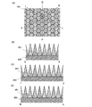
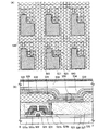
本発明は、複数の錐形凸部を隙間無く充填する構成を有することにより、表示画面表面側より外側(空気側)へ向かって錐形凸部という物理的な形状によって屈折率が変化していることを特徴とする。本発明において複数の錐形凸部の頂部は互いに等間隔に並んでおり、かつ錐形凸部において錐形を成す各底辺は隣接する他の錐形凸部の錐形を成す一底辺と接して設けられている。つまり、一つの錐形凸部は、周囲を他の錐形凸部に囲まれており、その錐形凸部の底面において錐形を成す各底辺はそれぞれ隣接する他の錐形凸部において錐形を成す一つの底辺と共有している。つまりその一つの錐形凸部において錐形の底面の各辺は、それぞれ隣接する他の錐形凸部と共有されている。 Since the present invention has a configuration in which a plurality of conical convex portions are filled without gaps, the refractive index changes depending on the physical shape of the conical convex portions from the display screen surface side toward the outer side (air side). It is characterized by being. In the present invention, the tops of the plurality of cone-shaped convex portions are arranged at equal intervals, and each base side forming the cone shape in the cone-shaped convex portion is in contact with one base side forming the cone shape of another adjacent cone-shaped convex portion. Is provided. That is, one cone-shaped convex portion is surrounded by another cone-shaped convex portion, and each base that forms a cone shape on the bottom surface of the cone-shaped convex portion is a cone in another adjacent cone-shaped convex portion. It is shared with one base that forms. That is, each side of the bottom surface of the conical shape in the one conical convex portion is shared with the other adjacent conical convex portions.
このように、隙間無く、頂部が等間隔になるように最密に充填し、光を効率よく多方向に散乱することのできる高い反射防止機能を有する。 In this way, it has a high antireflection function capable of efficiently scattering light in multiple directions, with the tops being packed closely so that the tops are equally spaced without gaps.
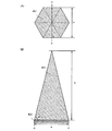
本発明において、複数の錐形凸部の頂部の間隔は350nm以下、複数の錐形凸部の高さは800nm以上であると好ましい。また、設けられる表示画面上において単位面積あたりの複数の錐形凸部の底面の充填率(表示画面上において充填する(占める)割合)は80%以上、好ましくは90%以上であると好ましい。充填率とは、表示画面における錐形凸部の形成領域の割合であり、充填率が80%以上であると、錐形凸部が形成されない平面(表示画面に対して平行であり、錐形凸部側面の斜面に対して平坦)部の割合は20%以下となる。また、錐形凸部の高さと底面の幅との比は5以上であると好ましい。 In the present invention, it is preferable that the interval between the tops of the plurality of conical convex portions is 350 nm or less, and the height of the plurality of conical convex portions is 800 nm or more. Further, the filling rate (ratio of filling (occupying) on the display screen) of the bottom surfaces of the plurality of conical convex portions per unit area on the provided display screen is 80% or more, preferably 90% or more. The filling rate is the ratio of the formation area of the cone-shaped projections on the display screen. When the filling rate is 80% or more, the plane on which the cone-shaped projections are not formed (parallel to the display screen, cone-shaped The ratio of the flat portion to the slope of the side surface of the convex portion is 20% or less. Moreover, it is preferable that the ratio between the height of the cone-shaped convex portion and the width of the bottom surface is 5 or more.
本発明により、隣接する複数の錐形凸部を有する反射防止フィルム(基板)、及び表示装置を提供することができ、高い反射防止機能を付与することができる。 According to the present invention, an antireflection film (substrate) having a plurality of adjacent conical convex portions and a display device can be provided, and a high antireflection function can be provided.
本発明は表示機能を有する装置である表示装置に用いることができ、本発明を用いる表示装置には、エレクトロルミネセンス(以下「EL」ともいう。)と呼ばれる発光を発現する有機物、無機物、若しくは有機物と無機物の混合物を含む層を、電極間に介在させた発光素子とTFTとが接続された発光表示装置や、液晶材料を有する液晶素子を表示素子として用いる液晶表示装置などがある。本発明において、表示装置とは、表示素子(液晶素子や発光素子など)を有する装置のことを言う。なお、基板上に液晶素子やEL素子などの表示素子を含む複数の画素やそれらの画素を駆動させる周辺駆動回路が形成された表示パネル本体のことでもよい。さらに、フレキシブルプリントサーキット(FPC)やプリント配線基盤(PWB)が取り付けられたもの(ICや抵抗素子や容量素子やインダクタやトランジスタなど)も含んでもよい。さらに、偏光板や位相差板などの光学シートを含んでいても良い。さらに、バックライト(導光板やプリズムシートや拡散シートや反射シートや光源(LEDや冷陰極管など)を含んでいても良い)を含んでいても良い。 The present invention can be used for a display device that is a device having a display function. The display device using the present invention includes an organic substance, an inorganic substance, or an organic substance that emits light called electroluminescence (hereinafter also referred to as “EL”). There are a light-emitting display device in which a light-emitting element in which a layer containing a mixture of an organic substance and an inorganic substance is interposed between electrodes and a TFT are connected, and a liquid crystal display device in which a liquid crystal element having a liquid crystal material is used as a display element. In the present invention, a display device refers to a device having a display element (such as a liquid crystal element or a light emitting element). Note that a display panel body in which a plurality of pixels including a display element such as a liquid crystal element or an EL element and a peripheral driver circuit for driving these pixels are formed over a substrate may be used. Furthermore, a device to which a flexible printed circuit (FPC) or a printed wiring board (PWB) is attached (such as an IC, a resistor, a capacitor, an inductor, or a transistor) may also be included. Furthermore, an optical sheet such as a polarizing plate or a retardation plate may be included. Furthermore, a backlight (which may include a light guide plate, a prism sheet, a diffusion sheet, a reflection sheet, or a light source (such as an LED or a cold cathode tube)) may be included.
なお、表示素子や表示装置は、様々な形態を用いたり、様々な素子を有することができる。例えば、EL素子(有機EL素子、無機EL素子又は有機物及び無機物を含むEL素子)、液晶素子、電子インクなど、電気的作用によりコントラストが変化する表示媒体を適用することができる。なお、EL素子を用いた表示装置としてはELディスプレイ、液晶素子を用いた表示装置としては液晶ディスプレイ、透過型液晶ディスプレイ、半透過型液晶ディスプレイ、反射型液晶ディスプレイ、電子インクを用いた表示装置としては電子ペーパーがある。 Note that the display element and the display device can have various forms or have various elements. For example, a display medium whose contrast is changed by an electric effect, such as an EL element (an organic EL element, an inorganic EL element, or an EL element including an organic substance and an inorganic substance), a liquid crystal element, and electronic ink, can be used. Note that an EL display is used as a display device using an EL element, and a display device using a liquid crystal element is a liquid crystal display, a transmissive liquid crystal display, a transflective liquid crystal display, a reflective liquid crystal display, and a display device using electronic ink. There is electronic paper.
本発明の反射防止フィルムの一形態は、複数の錐形凸部を有し、複数の錐形凸部の頂部は互いに等間隔に並んでおり、一の錐形凸部において錐形を成す各底辺は、隣接する錐形凸部において錐形を成す一の底辺と接するように配置される。 One form of the antireflection film of the present invention has a plurality of cone-shaped convex portions, and the top portions of the plurality of cone-shaped convex portions are arranged at equal intervals, and each cone-shaped convex portion forms a cone shape. The bottom side is arranged so as to be in contact with one bottom side forming a cone shape at the adjacent cone-shaped convex portion.
本発明の反射防止フィルムの一形態は、複数の錐形凸部を有し、複数の錐形凸部の頂部は互いに等間隔に並んでおり、一の錐形凸部の周囲には6個の隣接する錐形凸部が配置され、一の錐形凸部において錐形を成す各底辺は、隣接する錐形凸部において錐形を成す一の底辺と接するように配置される。 One form of the antireflection film of the present invention has a plurality of cone-shaped convex portions, and the top portions of the plurality of cone-shaped convex portions are arranged at equal intervals, and there are six pieces around one cone-shaped convex portion. Adjacent cone-shaped convex portions are arranged, and each base side forming a cone shape in one cone-shaped convex portion is arranged so as to be in contact with one base side forming a cone shape in the adjacent cone-shaped convex portion.
本発明の反射防止フィルムの一形態は、複数の錐形凸部を有し、複数の錐形凸部の頂部は互いに等間隔に並んでおり、一の錐形凸部において錐形を成す各底辺は、隣接する錐形凸部において錐形を成す一の底辺と接するように配置され、複数の錐形凸部の頂部の間隔は350nm以下であり、複数の錐形凸部の高さは800nm以上である。 One form of the antireflection film of the present invention has a plurality of cone-shaped convex portions, and the top portions of the plurality of cone-shaped convex portions are arranged at equal intervals, and each cone-shaped convex portion forms a cone shape. The bases are arranged so as to be in contact with one base that forms a conical shape in adjacent conical convex portions, the interval between the top portions of the plurality of conical convex portions is 350 nm or less, and the height of the plurality of conical convex portions is 800 nm or more.
本発明の反射防止フィルムの一形態は、複数の錐形凸部を有し、複数の錐形凸部の頂部は互いに等間隔に並んでおり、一の錐形凸部の周囲には6個の隣接する錐形凸部が配置され、一の錐形凸部において錐形を成す各底辺は、隣接する錐形凸部において錐形を成す一の底辺と接するように配置され、複数の錐形凸部の頂部の間隔は350nm以下であり、複数の錐形凸部の高さは800nm以上である。 One form of the antireflection film of the present invention has a plurality of cone-shaped convex portions, and the top portions of the plurality of cone-shaped convex portions are arranged at equal intervals, and there are six pieces around one cone-shaped convex portion. Adjacent cone-shaped convex portions are arranged, and each base side forming a cone shape in one cone-shaped convex portion is arranged so as to be in contact with one base side forming a cone shape in the adjacent cone-shaped convex portion, and a plurality of cones The space | interval of the top part of a shape convex part is 350 nm or less, and the height of several cone-shaped convex part is 800 nm or more.
本発明の反射防止フィルムの一形態は、複数の錐形凸部を有し、複数の錐形凸部の頂部は互いに等間隔に並んでおり、一の錐形凸部において錐形を成す各底辺は、隣接する錐形凸部において錐形を成す一の底辺と接するように配置され、複数の錐形凸部の頂部の間隔は350nm以下であり、複数の錐形凸部の高さは800nm以上であり、単位面積あたりの複数の錐形凸部の底面の充填率は80%以上である。 One form of the antireflection film of the present invention has a plurality of cone-shaped convex portions, and the top portions of the plurality of cone-shaped convex portions are arranged at equal intervals, and each cone-shaped convex portion forms a cone shape. The bases are arranged so as to be in contact with one base that forms a conical shape in adjacent conical convex portions, the interval between the top portions of the plurality of conical convex portions is 350 nm or less, and the height of the plurality of conical convex portions is It is 800 nm or more, and the filling rate of the bottom surfaces of the plurality of conical convex portions per unit area is 80% or more.
本発明の反射防止フィルムの一形態は、複数の錐形凸部を有し、複数の錐形凸部の頂部は互いに等間隔に並んでおり、一の錐形凸部の周囲には6個の隣接する錐形凸部が配置され、一の錐形凸部において錐形を成す各底辺は、隣接する錐形凸部において錐形を成す一の底辺と接するように配置され、複数の錐形凸部の頂部の間隔は350nm以下であり、複数の錐形凸部の高さは800nm以上であり、単位面積あたりの複数の錐形凸部の底面の充填率は80%以上である。 One form of the antireflection film of the present invention has a plurality of cone-shaped convex portions, and the top portions of the plurality of cone-shaped convex portions are arranged at equal intervals, and there are six pieces around one cone-shaped convex portion. Adjacent cone-shaped convex portions are arranged, and each base side forming a cone shape in one cone-shaped convex portion is arranged so as to be in contact with one base side forming a cone shape in the adjacent cone-shaped convex portion, and a plurality of cones The interval between the tops of the convex portions is 350 nm or less, the height of the plurality of conical convex portions is 800 nm or more, and the filling rate of the bottom surfaces of the plurality of conical convex portions per unit area is 80% or more.
本発明の反射防止フィルムの一形態は、複数の錐形凸部を有し、複数の錐形凸部の頂部は互いに等間隔に並んでおり、一の錐形凸部において錐形を成す各底辺は、隣接する錐形凸部において錐形を成す一の底辺と接するように配置され、複数の錐形凸部の頂部の間隔は350nm以下であり、複数の錐形凸部の高さは800nm以上であり、単位面積あたりの複数の錐形凸部の底面の充填率は80%以上であり、錐形凸部の高さと底面の幅との比は5以上である。 One form of the antireflection film of the present invention has a plurality of cone-shaped convex portions, and the top portions of the plurality of cone-shaped convex portions are arranged at equal intervals, and each cone-shaped convex portion forms a cone shape. The bases are arranged so as to be in contact with one base that forms a conical shape in adjacent conical convex portions, the interval between the top portions of the plurality of conical convex portions is 350 nm or less, and the height of the plurality of conical convex portions is The filling rate of the bottom surfaces of the plurality of conical convex portions per unit area is 80% or more, and the ratio of the height of the conical convex portions to the width of the bottom surface is 5 or more.
本発明の反射防止フィルムの一形態は、複数の錐形凸部を有し、複数の錐形凸部の頂部は互いに等間隔に並んでおり、一の錐形凸部の周囲には6個の隣接する錐形凸部が配置され、一の錐形凸部において錐形を成す各底辺は、隣接する錐形凸部において錐形を成す一の底辺と接するように配置され、複数の錐形凸部の頂部の間隔は350nm以下であり、複数の錐形凸部の高さは800nm以上であり、単位面積あたりの複数の錐形凸部の底面の充填率は80%以上であり、錐形凸部の高さと底面の幅との比は5以上である。 One form of the antireflection film of the present invention has a plurality of cone-shaped convex portions, and the top portions of the plurality of cone-shaped convex portions are arranged at equal intervals, and there are six pieces around one cone-shaped convex portion. Adjacent cone-shaped convex portions are arranged, and each base side forming a cone shape in one cone-shaped convex portion is arranged so as to be in contact with one base side forming a cone shape in the adjacent cone-shaped convex portion, and a plurality of cones The interval between the tops of the convex portions is 350 nm or less, the height of the plurality of conical convex portions is 800 nm or more, and the filling rate of the bottom surfaces of the plurality of conical convex portions per unit area is 80% or more, The ratio between the height of the cone-shaped convex portion and the width of the bottom surface is 5 or more.
本発明の表示装置の一形態は、一対の基板と、一対の基板間に設けられた表示素子と、一対の基板のうち少なくとも一方は透光性基板であり、透光性基板の外側に複数の錐形凸部を有し、複数の錐形凸部の頂部は互いに等間隔に並んでおり、一の錐形凸部において錐形を成す各底辺は、隣接する錐形凸部において錐形を成す一の底辺と接するように配置される。 One embodiment of a display device of the present invention includes a pair of substrates, a display element provided between the pair of substrates, and at least one of the pair of substrates is a light-transmitting substrate, and a plurality of the display devices are provided outside the light-transmitting substrate. The tops of the plurality of cone-shaped projections are arranged at equal intervals, and each base that forms a cone in one cone-shaped projection is conical in the adjacent cone-shaped projection. It is arrange | positioned so that the one base which comprises may be touched.
本発明の表示装置の一形態は、一対の基板と、一対の基板間に設けられた表示素子と、一対の基板のうち少なくとも一方は透光性基板であり、透光性基板の外側に複数の錐形凸部を有し、複数の錐形凸部の頂部は互いに等間隔に並んでおり、一の錐形凸部の周囲には6個の隣接する錐形凸部が配置され、一の錐形凸部において錐形を成す各底辺は、隣接する錐形凸部において錐形を成す一の底辺と接するように配置される。 One embodiment of a display device of the present invention includes a pair of substrates, a display element provided between the pair of substrates, and at least one of the pair of substrates is a light-transmitting substrate, and a plurality of the display devices are provided outside the light-transmitting substrate. The tops of the plurality of cone-shaped projections are arranged at equal intervals, and six adjacent cone-shaped projections are arranged around one cone-shaped projection. Each of the bases forming a conical shape in each of the conical convex portions is arranged so as to be in contact with one base forming the conical shape in the adjacent conical convex portions.
本発明の表示装置の一形態は、一対の基板と、一対の基板間に設けられた表示素子と、一対の基板のうち少なくとも一方は透光性基板であり、透光性基板の外側に複数の錐形凸部を有し、複数の錐形凸部の頂部は互いに等間隔に並んでおり、一の錐形凸部において錐形を成す各底辺は、隣接する錐形凸部において錐形を成す一の底辺と接するように配置され、複数の錐形凸部の頂部の間隔は350nm以下であり、複数の錐形凸部の高さは800nm以上である。 One embodiment of a display device of the present invention includes a pair of substrates, a display element provided between the pair of substrates, and at least one of the pair of substrates is a light-transmitting substrate, and a plurality of the display devices are provided outside the light-transmitting substrate. The tops of the plurality of cone-shaped projections are arranged at equal intervals, and each base that forms a cone in one cone-shaped projection is conical in the adjacent cone-shaped projection. Are arranged so as to be in contact with one bottom side, the interval between the tops of the plurality of conical convex portions is 350 nm or less, and the height of the plurality of conical convex portions is 800 nm or more.
本発明の表示装置の一形態は、一対の基板と、一対の基板間に設けられた表示素子と、一対の基板のうち少なくとも一方は透光性基板であり、透光性基板の外側に複数の錐形凸部を有し、複数の錐形凸部の頂部は互いに等間隔に並んでおり、一の錐形凸部の周囲には6個の隣接する錐形凸部が配置され、一の錐形凸部において錐形を成す各底辺は、隣接する錐形凸部において錐形を成す一の底辺と接するように配置され、複数の錐形凸部の頂部の間隔は350nm以下であり、複数の錐形凸部の高さは800nm以上である。 One embodiment of a display device of the present invention includes a pair of substrates, a display element provided between the pair of substrates, and at least one of the pair of substrates is a light-transmitting substrate, and a plurality of the display devices are provided outside the light-transmitting substrate. The tops of the plurality of cone-shaped projections are arranged at equal intervals, and six adjacent cone-shaped projections are arranged around one cone-shaped projection. In each of the cone-shaped convex portions, the bases forming the conical shape are arranged so as to contact one base forming the conical shape in the adjacent cone-shaped convex portions, and the interval between the top portions of the plurality of cone-shaped convex portions is 350 nm or less. The height of the plurality of conical convex portions is 800 nm or more.
本発明の表示装置の一形態は、一対の基板と、一対の基板間に設けられた表示素子と、一対の基板のうち少なくとも一方は透光性基板であり、透光性基板の外側に複数の錐形凸部を有し、複数の錐形凸部の頂部は互いに等間隔に並んでおり、一の錐形凸部において錐形を成す各底辺は、隣接する錐形凸部において錐形を成す一の底辺と接するように配置され、複数の錐形凸部の頂部の間隔は350nm以下であり、複数の錐形凸部の高さは800nm以上であり、単位面積あたりの複数の錐形凸部の底面の充填率は80%以上である。 One embodiment of a display device of the present invention includes a pair of substrates, a display element provided between the pair of substrates, and at least one of the pair of substrates is a light-transmitting substrate, and a plurality of the display devices are provided outside the light-transmitting substrate. The tops of the plurality of cone-shaped projections are arranged at equal intervals, and each base that forms a cone in one cone-shaped projection is conical in the adjacent cone-shaped projection. Are arranged so as to be in contact with one bottom side, the interval between the tops of the plurality of cone-shaped convex portions is 350 nm or less, the height of the plurality of cone-shaped convex portions is 800 nm or more, and a plurality of cones per unit area The filling rate of the bottom surface of the shape convex portion is 80% or more.
本発明の表示装置の一形態は、一対の基板と、一対の基板間に設けられた表示素子と、一対の基板のうち少なくとも一方は透光性基板であり、透光性基板の外側に複数の錐形凸部を有し、複数の錐形凸部の頂部は互いに等間隔に並んでおり、一の錐形凸部の周囲には6個の隣接する錐形凸部が配置され、一の錐形凸部において錐形を成す各底辺は、隣接する錐形凸部において錐形を成す一の底辺と接するように配置され、複数の錐形凸部の頂部の間隔は350nm以下であり、複数の錐形凸部の高さは800nm以上であり、単位面積あたりの複数の錐形凸部の底面の充填率は80%以上である。 One embodiment of a display device of the present invention includes a pair of substrates, a display element provided between the pair of substrates, and at least one of the pair of substrates is a light-transmitting substrate, and a plurality of the display devices are provided outside the light-transmitting substrate. The tops of the plurality of cone-shaped projections are arranged at equal intervals, and six adjacent cone-shaped projections are arranged around one cone-shaped projection. In each of the cone-shaped convex portions, the bases forming the conical shape are arranged so as to contact one base forming the conical shape in the adjacent cone-shaped convex portions, and the interval between the top portions of the plurality of cone-shaped convex portions is 350 nm or less. The height of the plurality of conical convex portions is 800 nm or more, and the filling rate of the bottom surfaces of the plurality of conical convex portions per unit area is 80% or more.
本発明の表示装置の一形態は、一対の基板と、一対の基板間に設けられた表示素子と、一対の基板のうち少なくとも一方は透光性基板であり、透光性基板の外側に複数の錐形凸部を有し、複数の錐形凸部の頂部は互いに等間隔に並んでおり、一の錐形凸部において錐形を成す各底辺は、隣接する錐形凸部において錐形を成す一の底辺と接するように配置され、複数の錐形凸部の頂部の間隔は350nm以下であり、複数の錐形凸部の高さは800nm以上であり、単位面積あたりの複数の錐形凸部の底面の充填率は80%以上であり、錐形凸部の高さと底面の幅との比は5以上である。 One embodiment of a display device of the present invention includes a pair of substrates, a display element provided between the pair of substrates, and at least one of the pair of substrates is a light-transmitting substrate, and a plurality of the display devices are provided outside the light-transmitting substrate. The tops of the plurality of cone-shaped projections are arranged at equal intervals, and each base that forms a cone in one cone-shaped projection is conical in the adjacent cone-shaped projection. Are arranged so as to be in contact with one bottom side, the interval between the tops of the plurality of cone-shaped convex portions is 350 nm or less, the height of the plurality of cone-shaped convex portions is 800 nm or more, and a plurality of cones per unit area The filling rate of the bottom surface of the shape convex portion is 80% or more, and the ratio of the height of the cone-shaped convex portion to the width of the bottom surface is 5 or more.
本発明の表示装置の一形態は、一対の基板と、一対の基板間に設けられた表示素子と、一対の基板のうち少なくとも一方は透光性基板であり、透光性基板の外側に複数の錐形凸部を有し、複数の錐形凸部の頂部は互いに等間隔に並んでおり、一の錐形凸部の周囲には6個の隣接する錐形凸部が配置され、一の錐形凸部において錐形を成す各底辺は、隣接する錐形凸部において錐形を成す一の底辺と接するように配置され、複数の錐形凸部の頂部の間隔は350nm以下であり、複数の錐形凸部の高さは800nm以上であり、単位面積あたりの複数の錐形凸部の底面の充填率は80%以上であり、錐形凸部の高さと底面の幅との比は5以上である。 One embodiment of a display device of the present invention includes a pair of substrates, a display element provided between the pair of substrates, and at least one of the pair of substrates is a light-transmitting substrate, and a plurality of the display devices are provided outside the light-transmitting substrate. The tops of the plurality of cone-shaped projections are arranged at equal intervals, and six adjacent cone-shaped projections are arranged around one cone-shaped projection. In each of the cone-shaped convex portions, the bases forming the conical shape are arranged so as to contact one base forming the conical shape in the adjacent cone-shaped convex portions, and the interval between the top portions of the plurality of cone-shaped convex portions is 350 nm or less. The height of the plurality of cone-shaped projections is 800 nm or more, the filling rate of the bottom surface of the plurality of cone-shaped projections per unit area is 80% or more, and the height of the cone-shaped projections and the width of the bottom surface The ratio is 5 or more.
錐形凸部は均一な屈折率でなく、表面(側面)から表示画面側に向かって屈折率が変化する材料で形成することができる。例えば、複数の錐形凸部において、錐形凸部表面側は空気と同等な屈折率を有する材料で形成し、より空気より錐形凸部に入射する外光の錐形凸部表面の反射を軽減する構造とする。一方、複数の錐形凸部において表示画面側の基板側に近づくにつれ基板と同等な屈折率を有する材料で形成し、錐形凸部内部を進行し、基板に入射する光の錐形凸部と基板との界面での反射を軽減する構成とする。 The cone-shaped convex portion is not a uniform refractive index but can be formed of a material whose refractive index changes from the surface (side surface) toward the display screen side. For example, in a plurality of cone-shaped convex portions, the surface of the cone-shaped convex portion is formed of a material having a refractive index equivalent to that of air, and reflection of the external light incident on the cone-shaped convex portion from the air is reflected from the air. A structure that reduces this. On the other hand, a plurality of cone-shaped convex portions are formed of a material having a refractive index equivalent to that of the substrate as they approach the substrate side on the display screen side, and travel inside the cone-shaped convex portions to be incident on the substrate. To reduce reflection at the interface between the substrate and the substrate.
基板にガラス基板を用いると、空気の屈折率の方がガラス基板よりも小さいため、錐形凸部は先端部の方が屈折率の低い材料で形成され、錐形凸部底面に近づくにつれ屈折率の高い材料で形成されるような、錐形凸部先端部より底面に向かって屈折率が増加するような構成とすればよい。基板にガラスを用いる場合、錐形凸部はフッ化物、酸化物、又は窒化物を含む膜で形成することができる。 If a glass substrate is used for the substrate, the refractive index of air is smaller than that of the glass substrate, so the cone-shaped convex part is formed of a material with a lower refractive index, and refracts as it approaches the bottom of the cone-shaped convex part. What is necessary is just to set it as the structure which a refractive index increases toward a bottom face from the front-end | tip part of a cone-shaped convex part formed with a material with a high rate. When glass is used for the substrate, the conical protrusions can be formed of a film containing fluoride, oxide, or nitride.
本発明の反射防止フィルム及び表示装置は、表面に隙間無く複数の錐形凸部を有しており、外光の反射光は錐形凸部側面が表示画面と平行でないので視認側に反射せず隣接する他の錐形凸部に反射する。もしくは錐形凸部と錐形凸部との間に進行する。錐形凸部は隙間無く最密に充填して設けることが可能な形状であり、そのような形状のなかでも最多な側面を有し、光を効率よく多方向に散乱することのできる高い反射防止機能を有する最適な形状である。入射した外光は錐形凸部に一部透過し反射光は隣接する錐形凸部にまた入射する。このように錐形凸部界面で反射された外光は隣接する他の錐形凸部に入射を繰り返す。 The antireflection film and the display device of the present invention have a plurality of conical convex portions on the surface with no gaps, and the reflected light of outside light is reflected to the viewing side because the side surfaces of the conical convex portions are not parallel to the display screen. Instead, the light is reflected on other adjacent cone-shaped convex portions. Or it progresses between a cone-shaped convex part and a cone-shaped convex part. The cone-shaped convex part is a shape that can be filled and packed closely without gaps, and it has the highest number of side surfaces among such shapes, and it is a highly reflective light that can efficiently scatter light in multiple directions. It is an optimal shape with a prevention function. The incident external light is partially transmitted through the cone-shaped convex portion, and the reflected light is incident on the adjacent cone-shaped convex portion again. Thus, the external light reflected at the interface of the cone-shaped convex portion repeats incident on the other adjacent cone-shaped convex portions.
つまり反射防止フィルムに入射する外光のうち、反射防止フィルムに入射する回数が増加するので、反射防止フィルムに透過する量が増える。よって、視認側に反射する外光が軽減され、写り込みなどの視認性を低下させる原因を防ぐことができる。 That is, among the external light incident on the antireflection film, the number of times of incidence on the antireflection film increases, so that the amount of light transmitted through the antireflection film increases. Therefore, the external light reflected on the viewer side is reduced, and the cause of lower visibility such as reflection can be prevented.
本発明は、表面に隣接する複数の錐形凸部を有することによってより外光の反射を軽減できる高い反射防止機能を有した視認性の優れた反射防止フィルム、及び表示装置を提供することができる。従って、より高画質及び高性能な表示装置を作製することができる。 The present invention provides an anti-reflection film with high visibility and a display device having a high anti-reflection function that can reduce reflection of external light by having a plurality of conical convex portions adjacent to the surface. it can. Therefore, a display device with higher image quality and higher performance can be manufactured.
以下に、本発明の実施の形態を図面に基づいて説明する。但し、本発明は多くの異なる態様で実施することが可能であり、本発明の趣旨及びその範囲から逸脱することなくその形態及び詳細を様々に変更し得ることは当業者であれば容易に理解される。従って、本実施の形態の記載内容に限定して解釈されるものではない。なお、実施の形態を説明するための全図において、同一部分又は同様な機能を有する部分には同一の符号を付し、その繰り返しの説明は省略する。 Embodiments of the present invention will be described below with reference to the drawings. However, the present invention can be implemented in many different modes, and those skilled in the art can easily understand that the modes and details can be variously changed without departing from the spirit and scope of the present invention. Is done. Therefore, the present invention is not construed as being limited to the description of this embodiment mode. Note that in all the drawings for describing the embodiments, the same portions or portions having similar functions are denoted by the same reference numerals, and repetitive description thereof is omitted.
(実施の形態1)
本実施の形態では、より外光の反射を軽減できる反射防止機能を有し優れた視認性を付与することを目的とした反射防止フィルムの一例について説明する。
(Embodiment 1)
In the present embodiment, an example of an antireflection film that has an antireflection function that can reduce reflection of external light and has excellent visibility will be described.
図1に本発明の反射防止フィルムの上面図及び断面図を示す。図1において表示装置450の表示画面上に複数の錐形凸部451が設けられている。図1(A)は本実施の形態の表示装置の上面図であり、図1(B)は図1(A)の線G−Hにおける断面図、図1(C)は図1(A)の線I−Jにおける断面図、図1(D)は図1(A)の線M−Nにおける断面図である。図1(A)(B)に示すように、錐形凸部451は表示画面上に充填するように隣接して設けられている。
FIG. 1 shows a top view and a cross-sectional view of the antireflection film of the present invention. In FIG. 1, a plurality of conical
反射防止フィルムにおいて、入射する外光に対して平面(表示画面と平行な面)が存在すると外光が視認側に反射してしまうため、平面の領域が少ない方が反射防止機能が高い。また、外光をより散乱するために反射防止フィルム表面は複数の角度を有する面によって構成される方が好ましい。 In the antireflection film, if there is a flat surface (a surface parallel to the display screen) with respect to incident external light, the external light is reflected to the viewer side. Therefore, the smaller the area of the flat surface, the higher the antireflection function. Moreover, in order to scatter external light more, it is preferable that the antireflection film surface is composed of surfaces having a plurality of angles.
本発明においては、複数の錐形凸部を幾何学的に隙間無く充填する構成を有することにより、表示画面表面側より外側(空気側)へ向かって錐形凸部という物理的な形状によって屈折率が変化している。本実施の形態において複数の錐形凸部の頂部は互いに等間隔に並んでおり、かつ錐形凸部において錐形を成す各底辺は隣接する他の錐形凸部の錐形を成す一底辺と接して設けられている。つまり、一つの錐形凸部は、周囲を他の錐形凸部に囲まれており、その錐形凸部の底面において錐形を成す各底辺はそれぞれ隣接する他の錐形凸部において錐形を成す一つの底辺と共有している。 In the present invention, by having a configuration in which a plurality of conical convex portions are filled geometrically without gaps, the refractive shape is refracted by the physical shape of the conical convex portions from the display screen surface side to the outside (air side). The rate is changing. In the present embodiment, the tops of the plurality of conical convex portions are arranged at equal intervals, and each base that forms a conical shape in the conical convex portion is one base that forms a conical shape of another adjacent conical convex portion. It is provided in contact with. That is, one cone-shaped convex portion is surrounded by another cone-shaped convex portion, and each base that forms a cone shape on the bottom surface of the cone-shaped convex portion is a cone in another adjacent cone-shaped convex portion. It is shared with one base that forms.
このように、隙間無く、頂部が等間隔になるように最密に充填し、光を効率よく多方向に散乱することのできる高い反射防止機能を有する。 In this way, it has a high antireflection function capable of efficiently scattering light in multiple directions, with the tops being packed closely so that the tops are equally spaced without gaps.
本実施の形態の複数の錐形凸部451は隣接する複数の錐形凸部の頂部と等間隔で設けられているため、図1(B)乃至(D)に示すように、同じ形状の断面となる。また、複数の錐形凸部は連続するように接して設けられ、錐形凸部の底面におけるすべての辺は隣り合う錐形凸部と接して設けられている。よって本実施の形態では図1(A)に示すように、複数の錐形凸部は、錐形凸部間に間隔を有さず、表示画面表面を覆っている。よって、図1(B)乃至(D)に示すように複数の錐形凸部によって表示画面表面の平面部は露出せず、入射する外光は複数の錐形凸部の斜面に入射するため、平面部での外光の反射を軽減することができる。また、表示画面表面における単位面積あたりの複数の錐形凸部の底面の占有率は80%以上、好ましくは90%以上であると、外光が平面部に入射する割合が軽減されるのでより視認者側への反射を防ぐことができる。
Since the plurality of conical
また錐形凸部において底面に対する角度が異なる側面が多い方が、より多方向に入射光を散乱するために好ましい。本実施の形態において、錐形凸部は6つの異なる角度で底面と接している側面を6つ有している。さらに、錐形凸部は、底面の頂点において他の複数の錐形凸部の頂点と接しており、それぞれ底面に対して角度を有している複数の側面に囲まれているのでより光を多方向に反射しやすい。従って、錐形凸部は底面において多くの頂点を有する方がより反射防止機能を発揮しやすく、本実施の形態の錐形凸部は底面に6つの頂点を有している。本実施の形態における六角形を底面として有する錐形凸部は隙間無く最密に充填して設けることが可能な形状であり、そのような形状のなかでも最多な側面を有し、光を効率よく多方向に散乱することのできる高い反射防止機能を有する最適な形状である。 Further, it is preferable that the cone-shaped convex portion has more side surfaces with different angles with respect to the bottom surface in order to scatter incident light in more directions. In the present embodiment, the cone-shaped convex portion has six side surfaces in contact with the bottom surface at six different angles. Furthermore, the cone-shaped convex portion is in contact with the vertices of the other plurality of cone-shaped convex portions at the vertex of the bottom surface, and is surrounded by a plurality of side surfaces each having an angle with respect to the bottom surface. Easy to reflect in multiple directions. Therefore, the cone-shaped convex portion has a larger number of vertices on the bottom surface and more easily exhibits an antireflection function, and the cone-shaped convex portion of the present embodiment has six vertices on the bottom surface. The cone-shaped convex portion having the hexagonal shape as the bottom surface in the present embodiment is a shape that can be filled and provided in a close-packed manner without any gaps, and has the most side surfaces among such shapes, and has light efficiency. It is an optimal shape with a high anti-reflection function that can scatter well in many directions.
本実施の形態の複数の錐形凸部451は隣接する複数の錐形凸部の頂部と等間隔で設けられているため、図1(B)乃至(D)に示すように、同じ形状の断面となる。
Since the plurality of conical
図3(A)に本発明の、隣接して充填している錐形凸部の例の上面図、図3(A)において線K−Lの断面図を図3(B)に示す。錐形凸部5000は周囲の錐形凸部5001a乃至5001fとそれぞれ底面の各辺(錐形を成す底辺)で接している。さらに錐形凸部5000、及び周囲を充填する錐形凸部5001a乃至5001fは底面が正六角形であり正六角形の中心に頂部5100、5101a乃至5101fが設けられている。従って錐形凸部5000の頂部5100は、接する錐形凸部5001a乃至5001fの各頂部5101a乃至5101fと等しい間隔pで有する。また、この場合、図3(B)に示すように、錐形凸部の頂部の間隔pと錐形凸部の幅aは等しくなる。
FIG. 3A shows a top view of an example of a conical convex portion filled adjacently according to the present invention, and FIG. 3B shows a cross-sectional view taken along line KL in FIG. 3A. The cone-shaped
図28に本発明を適用しない場合比較例を示す。図28(A)は底面が円である円錐状の錐形凸部(比較例1という)、(B)は底面が正方形で4つの側面を有する錐形凸部(比較例2という)、(C)は底面が正三角形であり3つの側面を有する錐形凸部(比較例3という)を充填した構成であり、それぞれの錐形凸部を上面よりみた上面図である。図28(A)に示すように、中央の円錐状の錐形凸部5200の周囲には最密充填構造で円錐状の錐形凸部5201a乃至5201fが並んでいる。しかし底面が円であるために最密充填構造をとっても錐形凸部5200と錐形凸部5201a乃至5201fとの間には間隔が生じてしまい、平面の表示画面が露出してしまう。平面において外光は視認側に反射してしまうため、比較例1の円錐状の錐形凸部の隣接する反射防止フィルムでは反射防止機能が低減してしまう。
FIG. 28 shows a comparative example when the present invention is not applied. 28A shows a conical convex portion having a circular bottom surface (referred to as Comparative Example 1), and FIG. 28B shows a conical convex portion having a square bottom surface and four side surfaces (referred to as Comparative Example 2). C) is a configuration in which the bottom surface is an equilateral triangle and is filled with conical convex portions (referred to as Comparative Example 3) having three side surfaces, and is a top view of the respective conical convex portions as seen from the top surface. As shown in FIG. 28A, conical cone-shaped
図28(B)は、中央の底面が正方形で4つの側面を有する錐形凸部5230の底面の正方形に接して底面が正方形で4つの側面を有する錐形凸部5231a乃至5231hが並んで充填している。同様に図28(C)は、中央の底面が正三角形であり3つの側面を有する錐形凸部5250の底面の三角形に接して底面が正三角形であり3つの側面を有する錐形凸部5251a乃至5251lが並んで充填している。本実施の形態の底面が六角形で6つの側面を有する錐形凸部では、隣接する錐形凸部において、その頂部の間隔を等しく並べることができるが、比較例2及び比較例3では図28(A)乃至(C)中にドットで示す錐形凸部の頂部の間隔が、すべて等しくなるように最密に並べることができない。また、比較例2及び比較例3は側面の数が本実施の形態と比べて少ないため、光を多方向に散乱させにくい。
In FIG. 28B, conical
比較例1、比較例2、及び本実施の形態における六角形で6つの側面を有する錐形凸部(構造Aという)において、光学計算を行った。本実施の形態においての計算は、光デバイス用光学計算シミュレータDiffract MOD(RSoft Design Group株式会社製)を用いている。反射率の計算を3次元で光学計算を行い計算する。比較例1、比較例2、構造Aにおいてそれぞれ光の波長と反射率の関係を図29に示す。また計算条件として上述の計算シミュレータのパラメータであるHarmonicsはX、Y方向ともに3に設定した。また、円錐形凸部や六角錐形凸部の場合、錐形凸部の頂部の間隔をp、錐形凸部の高さをbとして、上述の計算シミュレータのパラメータであるIndex Res.をX方向は√3×p/128分割、Y方向はp/128分割、Z方向はb/80で計算される数値に設定した。図28(B)に示すような四角錐形凸部の場合は、錐形凸部の頂部の間隔をqとして、上述の計算シミュレータのパラメータであるIndex Res.をX方向、Y方向は共にq/64、Z方向はb/80で計算される数値に設定した。 Optical calculation was performed on the hexagonal cone-shaped convex portion (referred to as structure A) in Comparative Example 1, Comparative Example 2, and the present embodiment. The calculation in the present embodiment uses an optical calculation simulator for optical devices, Diffract MOD (manufactured by RSSoft Design Group Co., Ltd.). The reflectance is calculated by performing optical calculation in three dimensions. FIG. 29 shows the relationship between the wavelength of light and the reflectance in Comparative Example 1, Comparative Example 2, and Structure A, respectively. As calculation conditions, Harmonics, which is a parameter of the above-described calculation simulator, is set to 3 in both the X and Y directions. Further, in the case of a conical convex portion or a hexagonal pyramidal convex portion, p is the interval between the apexes of the conical convex portion and b is the height of the conical convex portion, and the Index Res. Is set to a value calculated by √3 × p / 128 division in the X direction, p / 128 division in the Y direction, and b / 80 in the Z direction. In the case of a quadrangular pyramidal projection as shown in FIG. 28B, the interval between the apexes of the pyramidal projection is q, and Index Res. Are set to numerical values calculated by q / 64 in the X direction and Y direction, and b / 80 in the Z direction.
図29において、比較例1が丸のドット、比較例2が四角形のドット、構造Aが菱形のドットでありそれぞれの波長と反射率の関係を示している。光学計算結果においても本発明を適用する構造Aの錐形凸部を充填したモデルが測定した波長380nm〜780nmにおいて、他の比較例1や比較例2を充填した例よりも反射率が低く、最も反射が軽減できることが確認できる。なお、比較例1、比較例2、構造Aにおいてすべて屈折率は1.492、高さは1500nm、幅は300nmとしている。 In FIG. 29, the comparative example 1 is a round dot, the comparative example 2 is a square dot, and the structure A is a rhombus dot, showing the relationship between the wavelength and the reflectance. Also in the optical calculation result, the reflectivity is lower than the other examples filled with Comparative Example 1 and Comparative Example 2 at a wavelength of 380 nm to 780 nm measured by the model filled with the conical convex portion of the structure A to which the present invention is applied, It can be confirmed that reflection can be reduced most. In Comparative Example 1, Comparative Example 2, and Structure A, the refractive index is 1.492, the height is 1500 nm, and the width is 300 nm.
表示画面表面における単位面積あたりの複数の錐形凸部の底面の充填率は80%以上、好ましくは90%以上であると、外光が平面部に入射する割合が軽減されるのでより視認者側への反射を防ぐことができ、好ましい。充填率とは、表示画面における錐形凸部の形成領域の割合であり、充填率が80%以上であると、錐形凸部が形成されない平面(表示画面に対して平行であり、錐形凸部側面の斜面に対して平坦)部の割合は20%以下となる。 When the filling rate of the bottom surfaces of the plurality of conical convex portions per unit area on the display screen surface is 80% or more, preferably 90% or more, the proportion of external light incident on the flat portion is reduced, so that the viewer is more visible The reflection to the side can be prevented, which is preferable. The filling rate is the ratio of the formation area of the cone-shaped projections on the display screen. When the filling rate is 80% or more, the plane on which the cone-shaped projections are not formed (parallel to the display screen, cone-shaped The ratio of the flat portion to the slope of the side surface of the convex portion is 20% or less.
さらに本実施の形態における六角形で6つの側面を有する錐形凸部を充填したモデルにおいて、光の入射角度と反射率との関係を計算した光学計算結果を図30に示す。光の波長を550nmとし、幅は300nmで点線が高さ1500nmのモデル、実線が高さ3000nmのモデルの入射角度と反射率の関係である。反射率は60度以下において0.003%以下に低く抑えられており、60度、75度付近でも0.01%程度である。このことから本発明の錐形凸部充填モデルは広い入射角度において、反射率を低くすることができることが確認できる。 Further, FIG. 30 shows an optical calculation result obtained by calculating the relationship between the incident angle of light and the reflectance in the model in which the hexagonal pyramidal convex portion having six side surfaces is filled in the present embodiment. The light wavelength is 550 nm, the width is 300 nm, the dotted line is a model with a height of 1500 nm, and the solid line is the relationship between the incident angle and the reflectance of a model with a height of 3000 nm. The reflectance is kept low at 0.003% or less at 60 degrees or less, and is about 0.01% even at around 60 degrees and 75 degrees. From this, it can be confirmed that the cone-shaped convex portion filling model of the present invention can reduce the reflectance at a wide incident angle.
同様に本実施の形態における六角形で6つの側面を有する錐形凸部を充填したモデルにおいて、錐形凸部の幅a及び高さbを変化させて、各波長の光に対する反射率の変化を計算する。図31(A)乃至(C)に、高さbを500nm(菱形のドット)、800nm(ばつ印のドット)、1100nm(十字印のドット)、1400nm(丸印のドット)、1700nm(三角形のドット)、2000nm(四角形のドット)と変化させたときの、幅aに対する反射率Rの変化を示す。図33(A)乃至(C)に、幅aを100nm(菱形のドット)、160nm(ばつ印のドット)、220nm(十字印のドット)、280nm(黒い丸印のドット)、340nm(三角形のドット)、350nm(白抜きの丸印のドット)、400nm(四角形のドット)と変化させたときの、高さbに対する反射率Rの変化を示す。光の波長は可視光において青色を示す440nm(図31(A)図33(A))、緑色を示す550nm(図31(B)図33(B))、赤色を示す620nm(図31(C)図33(C))においてそれぞれ計算を行い、結果を示す。 Similarly, in the model filled with the hexagonal cone-shaped convex portion having six side faces in this embodiment, the width a and the height b of the cone-shaped convex portion are changed to change the reflectance with respect to light of each wavelength. Calculate 31A to 31C, the height b is 500 nm (diamond-shaped dots), 800 nm (cross-dot dots), 1100 nm (cross-dot dots), 1400 nm (circle-dot dots), 1700 nm (triangle-shaped dots). The change in the reflectance R with respect to the width a when the dot is changed to 2000 nm (square dot) is shown. 33A to 33C, the width a is 100 nm (diamond dot), 160 nm (dot symbol), 220 nm (cross symbol dot), 280 nm (black circle dot), 340 nm (triangle shape) The change in the reflectance R with respect to the height b is shown when the dot is changed to 350 nm (the white circle dot) and 400 nm (the square dot). The wavelength of light is 440 nm (FIG. 31 (A) and FIG. 33 (A)) showing blue in visible light, 550 nm (FIG. 31 (B) and FIG. 33 (B)) showing green, and 620 nm showing red (FIG. 31 (C)). ) In FIG. 33 (C)), each calculation is performed and the result is shown.
図31(A)乃至(C)に示すように、高さbにおいては800nm以上、幅aにおいては350nm以下(図31(A)におけるように更に好ましくは波長300nm以下)となると反射率は各波長においても0.01%以下となる。高さbは図33(A)乃至(C)に示すように800nm以上になると反射率が低くなり、0.015%以下という低い反射率に抑えられている。さらに高さbが1600nm以上になるとさらに、幅aの全測定範囲において反射率は0.005%以下という低い反射率に抑えられている。 As shown in FIGS. 31A to 31C, when the height b is 800 nm or more and the width a is 350 nm or less (more preferably, the wavelength is 300 nm or less as in FIG. The wavelength is 0.01% or less. As shown in FIGS. 33A to 33C, when the height b is 800 nm or more, the reflectance decreases, and is suppressed to a low reflectance of 0.015% or less. Further, when the height b is 1600 nm or more, the reflectance is further suppressed to a low reflectance of 0.005% or less in the entire measurement range of the width a.
図32(A)乃至(C)に、高さbを500nm(菱形のドット)、800nm(ばつ印のドット)、1100nm(十字印のドット)、1400nm(丸印のドット)、1700nm(三角形のドット)、2000nm(四角形のドット)と変化させたときの、高さbと幅aとの比(b/a)に対する反射率Rの変化を示す。図34(A)乃至(C)に、幅aを100nm(菱形のドット)、160nm(ばつ印のドット)、220nm(十字印のドット)、280nm(黒い丸印のドット)、340nm(三角形のドット)、350nm(白抜きの丸印のドット)、400nm(四角形のドット)と変化させたときの、高さbと幅aとの比(b/a)に対する反射率Rの変化を示す。光の波長は可視光において青色を示す440nm(図32(A)図34(A))、緑色を示す550nm(図32(B)図34(B))、赤色を示す620nm(図32(C)図34(C))においてそれぞれ計算を行い、結果を示す。 32A to 32C, the height b is 500 nm (diamond dot), 800 nm (cross mark dot), 1100 nm (cross mark dot), 1400 nm (circle mark dot), 1700 nm (triangle mark). The change in the reflectance R with respect to the ratio (b / a) between the height b and the width a when the dot is changed to 2000 nm (rectangular dot) is shown. 34A to 34C, the width a is 100 nm (diamond dot), 160 nm (dot symbol), 220 nm (cross symbol dot), 280 nm (black dot dot), 340 nm (triangle symbol) The change in the reflectance R with respect to the ratio (b / a) between the height b and the width a is shown when the dots are changed to 350 nm (open circle dots) and 400 nm (square dots). The wavelength of light is 440 nm (FIG. 32A and FIG. 34A) indicating blue in visible light, 550 nm (FIG. 32B and FIG. 34B) indicating green, and 620 nm indicating red (FIG. 32C). ) In FIG. 34 (C)), the respective calculations are performed and the results are shown.
図34(A)乃至(C)に示すデータを含む、幅aを100nmから400nmまで変化させたときの、高さbと幅aとの比(b/a)に対する反射率Rを平均したデータを図35に示す。図35は、波長440nm(菱形のドット)、550nm(四角形のドット)、620nm(三角形のドット)のときの、高さbと幅aとの比(b/a)と平均反射率との関係を示す。図34(A)乃至(C)に示すように高さbが800nm以上では高さbと幅aとの比(b/a)が大きくなると反射率は低下している。図35に示すように、高さbと幅aとの比(b/a)が5以上であれば平均反射率は全ての測定波長において0.01%以下となり、光の反射を抑える高い効果を得られることが確認できる。 Data including the data shown in FIGS. 34A to 34C, which is obtained by averaging the reflectance R with respect to the ratio (b / a) of the height b to the width a when the width a is changed from 100 nm to 400 nm. Is shown in FIG. FIG. 35 shows the relationship between the ratio of height b to width a (b / a) and average reflectance at wavelengths of 440 nm (diamond dots), 550 nm (square dots), and 620 nm (triangle dots). Indicates. As shown in FIGS. 34A to 34C, when the height b is 800 nm or more, the reflectance decreases as the ratio (b / a) between the height b and the width a increases. As shown in FIG. 35, if the ratio of height b to width a (b / a) is 5 or more, the average reflectance is 0.01% or less at all measurement wavelengths, and a high effect of suppressing light reflection. Can be confirmed.
複数の錐形凸部の幅は複数の錐形凸部の頂部の間隔と等しいので、以上のことより、複数の錐形凸部の頂部の間隔は350nm以下(より好ましくは100nm以上300nm以下)、複数の錐形凸部の高さは800nm以上(より好ましくは1000nm、1600nm以上2000nm以下)であると好ましい。また、錐形凸部において、錐形凸部の高さと底面における幅との比は5以上が好ましい。 Since the width of the plurality of conical convex portions is equal to the interval between the top portions of the plurality of conical convex portions, the interval between the top portions of the plurality of conical convex portions is 350 nm or less (more preferably, 100 nm or more and 300 nm or less). The height of the plurality of conical convex portions is preferably 800 nm or more (more preferably 1000 nm, 1600 nm or more and 2000 nm or less). Further, in the conical convex portion, the ratio of the height of the conical convex portion to the width at the bottom is preferably 5 or more.
図2(A)(B)に、図1における反射防止機能を有する錐形凸部の拡大図を示す。図2(A)は錐形凸部上面図であり、図2(B)は図2(A)の線O−Pにおける断面図である。線O―Pは錐形凸部底面において中心を通り辺に垂直な線であり、図2(B)に示すように錐形凸部の側面と底面とは角度(θ)をとっている。本明細書では、錐形凸部底面において中心を通り辺に垂直な線の長さを錐形凸部の底面の幅aという。また錐形凸部底面より頂部までの長さを錐形凸部の高さbという。 2A and 2B are enlarged views of the cone-shaped convex portion having the antireflection function in FIG. 2A is a top view of the conical convex portion, and FIG. 2B is a cross-sectional view taken along line OP in FIG. 2A. The line OP is a line passing through the center and perpendicular to the side at the bottom surface of the cone-shaped convex portion, and the side surface and the bottom surface of the cone-shaped convex portion form an angle (θ) as shown in FIG. In the present specification, the length of a line passing through the center and perpendicular to the side on the bottom surface of the conical convex portion is referred to as a width a of the bottom surface of the conical convex portion. The length from the bottom of the cone-shaped convex part to the top is called the height b of the cone-shaped convex part.
錐形凸部の形状は、錐形凸部の先端が平面であり、断面が台形の形状、先端が丸いドーム状、又は角柱と錐形凸部が積層された形状であってもよい。錐形凸部の形状の例を図27(A)乃至(C)に示す。図27(A)は、錐形凸部形のように先がとがっている形状ではなく、上面(幅a2)と底面(幅a1)を有する形状である。よって底面と垂直な面における断面図では、台形の形状となる。図27(A)のような表示装置490上に設けられる錐形凸部491において、本発明では、下底面から上底面までを高さbとする。
The shape of the cone-shaped convex portion may be a shape in which the tip of the cone-shaped convex portion is a flat surface and has a trapezoidal cross section, a dome shape with a rounded tip, or a shape in which a prism and a cone-shaped convex portion are stacked. Examples of the shape of the cone-shaped convex portion are shown in FIGS. FIG. 27A shows a shape having a top surface (width a2) and a bottom surface (width a1) instead of a pointed shape like a cone-shaped convex shape. Therefore, the cross-sectional view in the plane perpendicular to the bottom surface has a trapezoidal shape. In the conical
図27(B)は表示装置470上に、先端が丸い錐形凸部471が設けられた例である。このように錐形凸部は先端が丸く曲率を有する形状でもよく、この場合、錐形凸部の高さbは、底面より先端部の最も高い位置までとする。
FIG. 27B illustrates an example in which a cone-shaped
図27(C)は表示装置480上に、複数の角度θ1及びθ2を有する錐形凸部481が設けられた例である。このように錐形凸部は、六角柱状の形状に錐形凸部状の形状が積層されるような形状でもよい。この場合側面と底面の角度はθ1及びθ2と異なることになる。図27(C)のような錐形凸部481の場合、高さbは錐形凸部側面が斜行する錐形状の部分の高さとする。
FIG. 27C illustrates an example in which a cone-shaped
図1は複数の錐形凸部が底面で接して充填する構成であるが、膜(基板)上部の表面に錐形凸部を設ける構成でもよい。図36(A)乃至(D)は図1において、錐形凸部の側面が表示画面に達さず、複数の錐形凸部を表面に有する膜486の形状で設けられている例を示す。本発明の反射防止フィルムは隣接して充填されている錐形凸部を有する構成であればよく、膜(基板)表面に直接錐形凸部を一体の連続構造として作り込んでもよく、例えば膜(基板)表面を加工し、錐形凸部を作り込んでもよいし、ナノインプリント等の印刷法で錐形凸部を有する形状に選択的に形成してもよい。また、錐形凸部を別工程で膜(基板)上に形成してもよい。
Although FIG. 1 shows a configuration in which a plurality of conical convex portions are in contact with each other on the bottom surface, a conical convex portion may be provided on the upper surface of the film (substrate). 36A to 36D show an example in which the side surface of the conical convex portion does not reach the display screen in FIG. 1 and is provided in the shape of a
複数の錐形凸部は一体の連続膜としてもよいし、複数の錐形凸部を基板上に設ける構成としてもよい。またあらかじめ基板に錐形凸部を作りこんでもよい。錐形凸部を設ける基板としては、ガラス基板や石英基板等も用いることができる。また可撓性基板を用いてもよい。可撓性基板とは、折り曲げることができる(フレキシブル)基板のことであり、例えば、ポリカーボネート、ポリアリレート、ポリエーテルスルフォン等からなる、プラスチック基板の他、高温では可塑化されてプラスチックと同じような成型加工が出来、常温ではゴムのような弾性体の性質を示す高分子材料エラストマー等が挙げられる。また、フィルム(ポリプロピレン、ポリエステル、ビニル、ポリフッ化ビニル、塩化ビニルなどからなる)、無機蒸着フィルムを用いることもできる。複数の錐形凸部は基板を加工して作りこんでもよいし、成膜などによって基板上に形成してもよい。また、別工程で錐形凸部を形成し接着剤などで基板上に貼り付けてもよい。反射防止フィルムを他の表示装置の画面上に設ける場合も、粘着剤や接着剤等で貼り付けて設けることができる。このように、本発明の反射防止フィルムは複数の錐形凸部を有する様々な形状を適用して形成することができる。 The plurality of conical convex portions may be formed as an integral continuous film, or the plurality of conical convex portions may be provided on the substrate. Further, a conical convex portion may be formed in advance on the substrate. A glass substrate, a quartz substrate, or the like can also be used as the substrate on which the conical protrusions are provided. A flexible substrate may be used. A flexible substrate is a substrate that can be bent (flexible). For example, a plastic substrate made of polycarbonate, polyarylate, polyethersulfone, etc., or plasticized at a high temperature and similar to plastic. Examples thereof include high-molecular material elastomers that can be molded and exhibit the properties of elastic bodies such as rubber at room temperature. Moreover, a film (made of polypropylene, polyester, vinyl, polyvinyl fluoride, vinyl chloride, etc.) or an inorganic vapor deposition film can also be used. The plurality of conical convex portions may be formed by processing the substrate, or may be formed on the substrate by film formation or the like. Alternatively, the conical projections may be formed in a separate process and attached to the substrate with an adhesive or the like. In the case where the antireflection film is provided on the screen of another display device, the antireflection film can be provided by being attached with an adhesive or an adhesive. Thus, the antireflection film of the present invention can be formed by applying various shapes having a plurality of conical convex portions.
また、錐形凸部は均一な屈折率でなく、表面から表示画面側に向かって屈折率が変化する材料で形成することができる。例えば、複数の錐形凸部において、錐形凸部表面側は空気と同等な屈折率を有する材料で形成し、より空気より錐形凸部に入射する外光の錐形凸部表面の反射を軽減する構造とする。一方、複数の錐形凸部において表示画面側の基板側に近づくにつれ基板と同等な屈折率を有する材料で形成し、錐形凸部内部を進行し、基板に入射する光の錐形凸部と基板との界面での反射を軽減する構成とする。基板にガラス基板を用いると、空気の屈折率の方がガラス基板よりも小さいため、錐形凸部先端部の方が屈折率の低い材料で形成され、錐形凸部底面に近づくにつれ屈折率の高い材料で形成されるような、錐形凸部先端部より底面に向かって屈折率が増加するような構成とすればよい。 In addition, the cone-shaped convex portion can be formed of a material whose refractive index changes from the surface toward the display screen instead of a uniform refractive index. For example, in a plurality of cone-shaped convex portions, the surface of the cone-shaped convex portion is formed of a material having a refractive index equivalent to that of air, and reflection of the external light incident on the cone-shaped convex portion from the air is reflected from the air. A structure that reduces this. On the other hand, a plurality of cone-shaped convex portions are formed of a material having a refractive index equivalent to that of the substrate as they approach the substrate side on the display screen side, and travel inside the cone-shaped convex portions to be incident on the substrate. To reduce reflection at the interface between the substrate and the substrate. When a glass substrate is used as the substrate, the refractive index of air is smaller than that of the glass substrate, so the tip of the cone-shaped convex part is made of a material with a lower refractive index, and the refractive index is closer to the bottom of the cone-shaped convex part. What is necessary is just to set it as the structure which a refractive index increases toward a bottom face from the front-end | tip part of a cone-shaped convex part formed with a high material.
錐形凸部を形成する材料としては珪素、窒素、フッ素、酸化物、窒化物、フッ化物など表示画面表面を構成する基板の材料に応じて適宜設定すればよい。酸化物としては、酸化珪素(SiO2)、ホウ酸(B2O3)、酸化ナトリウム(NaO2)、酸化マグネシウム(MgO)、酸化アルミニウム(アルミナ)(Al2O3)、酸化カリウム(K2O)、酸化カルシウム(CaO)、三酸化二ヒ素(亜ヒ酸)(As2O3)、酸化ストロンチウム(SrO)、酸化アンチモン(Sb2O3)、酸化バリウム(BaO)、インジウム錫酸化物(ITO)、酸化亜鉛(ZnO)、酸化インジウムに酸化亜鉛(ZnO)を混合したIZO(indium zinc oxide)、酸化インジウムに酸化珪素(SiO2)を混合した導電材料、有機インジウム、有機スズ、酸化タングステンを含むインジウム酸化物、酸化タングステンを含むインジウム亜鉛酸化物、酸化チタンを含むインジウム酸化物、酸化チタンを含むインジウム錫酸化物などを用いることができる。窒化物としては、窒化アルミニウム(AlN)、窒化珪素(SiN)などを用いることができる。フッ化物としては、フッ化リチウム(LiF)、フッ化ナトリウム(NaF)、フッ化マグネシウム(MgF2)、フッ化カルシウム(CaF2)、フッ化ランタン(LaF3)などを用いることができる。前記珪素、窒素、フッ素、酸化物、窒化物、フッ化物は単数及び複数種を含んでいてもよく、その混合比は各基板の成分比(組成割合)によって適宜設定すればよい。 What is necessary is just to set suitably as a material which forms a cone-shaped convex part according to the material of the board | substrate which comprises the display screen surface, such as silicon, nitrogen, a fluorine, an oxide, nitride, and fluoride. Examples of the oxide include silicon oxide (SiO 2 ), boric acid (B 2 O 3 ), sodium oxide (NaO 2 ), magnesium oxide (MgO), aluminum oxide (alumina) (Al 2 O 3 ), and potassium oxide (K 2 O), calcium oxide (CaO), arsenic trioxide (arsenous acid) (As 2 O 3 ), strontium oxide (SrO), antimony oxide (Sb 2 O 3 ), barium oxide (BaO), indium tin oxide (ITO), zinc oxide (ZnO), indium oxide mixed with zinc oxide (ZnO) IZO (indium zinc oxide), indium oxide mixed with silicon oxide (SiO 2 ), conductive material, organic indium, organic tin, Indium oxide containing tungsten oxide, Indium zinc oxide containing tungsten oxide, Titanium oxide included Indium oxide, or the like can be used indium tin oxide containing titanium oxide. As the nitride, aluminum nitride (AlN), silicon nitride (SiN), or the like can be used. As the fluoride, lithium fluoride (LiF), sodium fluoride (NaF), magnesium fluoride (MgF 2 ), calcium fluoride (CaF 2 ), lanthanum fluoride (LaF 3 ), or the like can be used. The silicon, nitrogen, fluorine, oxide, nitride, and fluoride may include one or more kinds, and the mixing ratio may be set as appropriate depending on the component ratio (composition ratio) of each substrate.
錐形凸部はスパッタリング法、真空蒸着法、PVD法(Physical Vapor Deposition)、減圧CVD法(LPCVD法)、またはプラズマCVD法等のCVD法(Chemical Vapor Deposition)により薄膜を成膜した後、所望の形状にエッチングして形成することができる。また、選択的にパターンを形成できる液滴吐出法や、パターンが転写または描写できる印刷法(スクリーン印刷やオフセット印刷などパターンが形成される方法)、その他スピンコート法などの塗布法、ディッピング法、ディスペンサ法、刷毛塗り法、スプレー法、フローコート法などを用いることもできる。また、インプリント技術、nmレベルの立体構造物を転写技術で形成できるナノインプリント技術を用いることもができる。インプリント、ナノインプリントは、フォトリソグラフィー工程を用いずに微細な立体構造物を形成できる技術である。 The cone-shaped convex portion is formed by a thin film by a sputtering method, a vacuum deposition method, a PVD method (Physical Vapor Deposition), a low pressure CVD method (LPCVD method), or a CVD method (Chemical Vapor Deposition) such as a plasma CVD method, and then the desired shape. It can be formed by etching into the shape. In addition, a droplet discharge method that can selectively form a pattern, a printing method that can transfer or depict a pattern (a method that forms a pattern such as screen printing or offset printing), other coating methods such as spin coating, dipping method, A dispenser method, a brush coating method, a spray method, a flow coating method, or the like can also be used. In addition, an imprint technique and a nanoimprint technique capable of forming a three-dimensional structure at the nm level by a transfer technique can also be used. Imprinting and nanoimprinting are techniques that can form fine three-dimensional structures without using a photolithography process.
本発明の複数の錐形凸部を有する反射防止フィルムにおける反射防止機能を図25を用いて説明する。図25に、表示装置410の表示画面上に隣接する錐形凸部411a、411b、411c、411dが充填するように設けられている。外光412aは錐形凸部411cに入射し、一部が透過光413aとなって透過し、他は錐形凸部411c界面で反射光412bとなって反射される。反射光412bは隣接する錐形凸部411bに再び入射し、一部が透過光413bとなって透過し、他は錐形凸部411b界面で反射光412cとなって反射される。反射光412cは再び隣接する錐形凸部411cに入射し、一部が透過光413cとなって透過し、他は錐形凸部411c界面で反射光412dとなって反射される。反射光412dも再び隣接する錐形凸部411bに入射し、一部が透過光413dとなって透過する。
The antireflection function in the antireflection film having a plurality of conical convex portions of the present invention will be described with reference to FIG. In FIG. 25, adjacent conical
このように本実施の形態の反射防止フィルムは、表面に複数の錐形凸部を有しており、外光の反射光は錐形凸部界面が平面ではないので視認側に反射せず隣接する他の錐形凸部に反射する。もしくは錐形凸部と錐形凸部の間に進行する。入射した外光は錐形凸部に一部透過し反射光は隣接する錐形凸部にまた入射する。このように錐形凸部界面で反射された外光は隣接する他の錐形凸部に入射を繰り返す。 As described above, the antireflection film of the present embodiment has a plurality of conical convex portions on the surface, and the reflected light of outside light is not reflected on the viewer side because the interface of the conical convex portions is not flat, and is adjacent. Reflects on other cone-shaped convex parts. Or it progresses between a cone-shaped convex part and a cone-shaped convex part. The incident external light is partially transmitted through the cone-shaped convex portion, and the reflected light is incident on the adjacent cone-shaped convex portion again. Thus, the external light reflected at the interface of the cone-shaped convex portion repeats incident on the other adjacent cone-shaped convex portions.
つまり反射防止フィルムに入射する外光のうち、反射防止フィルムの有する錐形凸部に入射する回数が増加するので、反射防止フィルムに透過する量が増える。よって、視認側に反射する外光が軽減され、写り込みなどの視認性を低下させる原因を防ぐことができる。 That is, among the external light incident on the antireflection film, the number of times of incidence on the cone-shaped convex portion of the antireflection film increases, so that the amount transmitted to the antireflection film increases. Therefore, the external light reflected on the viewer side is reduced, and the cause of lower visibility such as reflection can be prevented.
本発明は、表面に隣接する複数の錐形凸部を有することによってより外光の反射を軽減できる高い反射防止機能を有した視認性の優れた反射防止フィルム、及び表示装置を提供することができる。従って、より高画質及び高性能な表示装置を作製することができる。 The present invention provides an anti-reflection film with high visibility and a display device having a high anti-reflection function that can reduce reflection of external light by having a plurality of conical convex portions adjacent to the surface. it can. Therefore, a display device with higher image quality and higher performance can be manufactured.
(実施の形態2)
本実施の形態では、より外光の反射を軽減できる反射防止機能を有し優れた視認性を付与することを目的とした表示装置の一例について説明する。より具体的には、表示装置の構成がパッシブマトリクス型の場合に関して示す。
(Embodiment 2)
In this embodiment, an example of a display device which has an antireflection function that can reduce reflection of external light and has excellent visibility will be described. More specifically, the case where the structure of the display device is a passive matrix type will be described.
表示装置は、第1の方向に延びた第1の電極層751a、第1の電極層751b、第1の電極層751c、第1の電極層751a、第1の電極層751b及び第1の電極層751cを覆って設けられた電界発光層752と、第1の方向と垂直な第2の方向に延びた第2の電極層753a、第2の電極層753b、第2の電極層753cとを有している(図5(A)(B)参照。)。第1の電極層751a、第1の電極層751b、第1の電極層751cと第2の電極層753a、第2の電極層753b、第2の電極層753cとの間に電界発光層752が設けられている。また、第2の電極層753a、第2の電極層753b、第2の電極層753cを覆うように、保護膜として機能する絶縁層754を設けている(図5(A)(B)参照。)。なお、隣接する各々の発光素子間において横方向への電界の影響が懸念される場合は、各発光素子に設けられた電界発光層752を分離してもよい。
The display device includes a
図5(C)は、図5(B)の変形例であり、第1の電極層791a、第1の電極層791b、第1の電極層791c、電界発光層792、第2の電極層793b、保護層である絶縁層794が、基板799上に設けられている。図5(C)の第1の電極層791a、第1の電極層791b、第1の電極層791cのように、第1の電極層は、テーパーを有する形状でもよく、曲率半径が連続的に変化する形状でもよい。第1の電極層791a、第1の電極層791b、第1の電極層791cのような形状は、液滴吐出法などを用いて形成することができる。このような曲率を有する曲面であると、積層する絶縁層や導電層のカバレッジがよい。
FIG. 5C is a modification example of FIG. 5B, and includes a
また、第1の電極層の端部を覆うように隔壁(絶縁層)を形成してもよい。隔壁(絶縁層)は、他の発光素子間を隔てる壁のような役目を果たす。図6(A)、(B)に第1の電極層の端部を隔壁(絶縁層)で覆う構造を示す。 In addition, a partition wall (insulating layer) may be formed so as to cover an end portion of the first electrode layer. The partition wall (insulating layer) serves as a wall separating other light emitting elements. 6A and 6B illustrate a structure in which the end portion of the first electrode layer is covered with a partition wall (insulating layer).
図6(A)に示す発光素子の一例は、隔壁(絶縁層)775が、第1の電極層771a、第1の電極層771b、第1の電極層771cの端部を覆うようにテーパーを有する形状で形成されている。基板779に接して設けられた第1の電極層771a、第1の電極層771b、第1の電極層771c上に、隔壁(絶縁層)775を形成し、電界発光層772、第2の電極層773b、絶縁層774、絶縁層776、基板778が設けられている。
6A, the partition wall (insulating layer) 775 is tapered so as to cover end portions of the
図6(B)に示す発光素子の一例は、隔壁(絶縁層)765が曲率を有し、その曲率半径が連続的に変化する形状である。第1の電極層761a、第1の電極層761b、第1の電極層761c、電界発光層762、第2の電極層763b、絶縁層764、保護層768に接して設けられている。
An example of the light-emitting element illustrated in FIG. 6B has a shape in which the partition wall (insulating layer) 765 has a curvature, and the radius of curvature continuously changes. The
図4は、本発明を適用したパッシブマトリクス型の液晶表示装置を示す。図4において、第1の画素電極層1701a、1701b、1701c、配向膜として機能する絶縁層1712が設けられた基板1700と、配向膜として機能する絶縁層1704、対向電極層1705、カラーフィルタとして機能する着色層1706、偏光板1714が設けられた基板1710とが液晶層1703を挟持して対向している。
FIG. 4 shows a passive matrix liquid crystal display device to which the present invention is applied. In FIG. 4, a
本発明では、表示装置において、表示画面表面に外光の反射を防止する反射防止機能を付与するため、最密に充填された複数の錐形凸部を表示画面上に設けることを特徴とする。本実施の形態において表示画面視認側である基板758、798、778、769、1710表面に錐形凸部757、797、777、767、1707が設けられている。
According to the present invention, in the display device, a plurality of closely packed cone-shaped convex portions are provided on the display screen in order to provide an antireflection function for preventing reflection of external light on the display screen surface. . In this embodiment, conical
本実施の形態の表示装置は隣接して充填されている錐形凸部を有する構成であればよく、表示画面を構成する基板(膜)表面に直接錐形凸部を一体の連続構造として作り込んでもよく、例えば基板(膜)表面を加工し、錐形凸部を作り込んでもよいし、ナノインプリント等の印刷法で錐形凸部を有する形状に選択的に形成してもよい。また、錐形凸部を別工程で膜(基板)上に形成してもよい。 The display device of the present embodiment only needs to have a conical convex portion filled adjacently, and the conical convex portion is directly formed on the surface of the substrate (film) constituting the display screen as an integral continuous structure. For example, the surface of the substrate (film) may be processed to form a conical convex portion, or may be selectively formed into a shape having the conical convex portion by a printing method such as nanoimprinting. Moreover, you may form a cone-shaped convex part on a film | membrane (board | substrate) by another process.
複数の錐形凸部は一体の連続膜としてもよいし、複数の錐形凸部を充填するように並べて基板上に設ける構成としてもよい。またあらかじめ基板に錐形凸部を作りこんでもよい。図6(A)は、基板778表面に複数の錐形凸部777が一体の連続構造として設けられた例である。
The plurality of conical convex portions may be formed as an integral continuous film, or may be arranged on the substrate side by side so as to fill the plurality of conical convex portions. Further, a conical convex portion may be formed in advance on the substrate. FIG. 6A shows an example in which a plurality of conical
表示画面において、入射する外光に対して平面(表示画面と平行な面)が存在すると外光が視認側に反射してしまうため、平面の領域が少ない方が反射防止機能が高い。また、外光をより散乱するために表示画面表面は複数の角度を有する面によって構成される方が好ましい。 In the display screen, if there is a plane (a plane parallel to the display screen) with respect to incident external light, the external light is reflected to the viewer side. Moreover, in order to scatter external light more, it is preferable that the display screen surface is constituted by surfaces having a plurality of angles.
本発明においては、複数の錐形凸部を隙間無く充填する構成を有することにより、表示画面表面側より外側(空気側)へ向かって錐形凸部という物理的な形状によって屈折率が変化している。本実施の形態において複数の錐形凸部の頂部は互いに等間隔に並んでおり、かつ錐形凸部において錐形を成す各底辺は隣接する他の錐形凸部の錐形を成す一底辺と接して設けられている。つまり、一つの錐形凸部は、周囲を他の錐形凸部に囲まれており、その錐形凸部の底面において錐形を成す各底辺はそれぞれ隣接する他の錐形凸部において錐形を成す一つの底辺と共有している。 In the present invention, by having a configuration in which a plurality of conical convex portions are filled without gaps, the refractive index changes depending on the physical shape of the conical convex portions from the display screen surface side toward the outside (air side). ing. In the present embodiment, the tops of the plurality of conical convex portions are arranged at equal intervals, and each base that forms a conical shape in the conical convex portion is one base that forms a conical shape of another adjacent conical convex portion. It is provided in contact with. That is, one cone-shaped convex portion is surrounded by another cone-shaped convex portion, and each base that forms a cone shape on the bottom surface of the cone-shaped convex portion is a cone in another adjacent cone-shaped convex portion. It is shared with one base that forms.
このように、隙間無く、頂部が等間隔になるように最密に充填し、光を効率よく多方向に散乱することのできる高い反射防止機能を有する。 In this way, it has a high antireflection function capable of efficiently scattering light in multiple directions, with the tops being packed closely so that the tops are equally spaced without gaps.
本実施の形態の複数の錐形凸部451は隣接する複数の錐形凸部の頂部と等間隔で設けられているため、図4、図5(A)乃至(C)、図6(A)(B)に示すように、同じ形状の断面となる。また、複数の錐形凸部451は連続するように接して設けられ、錐形凸部の底面における錐形を成す各底辺は隣り合う凸部の底面における錐形を成す一底辺と接して設けられている。よって本実施の形態では図4、図5(A)乃至(C)、図6(A)(B)に示すように、複数の錐形凸部は、凸部間に間隔を有さず、表示画面表面を覆っている。従って、複数の錐形凸部によって表示画面表面の平面部は露出せず、入射する外光は複数の錐形凸部の斜面に入射するため、平面部での外光の反射を軽減することができる。
Since the plurality of conical
本実施の形態において、複数の錐形凸部の頂部の間隔及び錐形凸部の底面の幅は350nm以下、複数の錐形凸部の高さは800nm以上であると好ましい。また、設けられる表示画面上において単位面積あたりの複数の錐形凸部の底面の充填率(表示画面上において充填する(占める)割合)は80%以上、好ましくは90%以上であると好ましい。充填率とは、表示画面における錐形凸部の形成領域の割合であり、充填率が80%以上であると、錐形凸部が形成されない平面(表示画面に対して平行であり、錐形凸部側面の斜面に対して平坦)部の割合は20%以下となる。また、錐形凸部の高さと底面の幅との比は5以上であると好ましい。上記条件であると、外光が平面部に入射する割合が軽減されるのでより視認者側への反射を防ぐことができる。 In the present embodiment, it is preferable that the interval between the top portions of the plurality of conical convex portions and the width of the bottom surface of the conical convex portions are 350 nm or less, and the height of the plurality of conical convex portions is 800 nm or more. Further, the filling rate (ratio of filling (occupying) on the display screen) of the bottom surfaces of the plurality of conical convex portions per unit area on the provided display screen is 80% or more, preferably 90% or more. The filling rate is the ratio of the formation area of the cone-shaped projections on the display screen. When the filling rate is 80% or more, the plane on which the cone-shaped projections are not formed (parallel to the display screen, cone-shaped The ratio of the flat portion to the slope of the side surface of the convex portion is 20% or less. Moreover, it is preferable that the ratio between the height of the cone-shaped convex portion and the width of the bottom surface is 5 or more. When the above conditions are satisfied, since the ratio of the external light incident on the flat surface portion is reduced, reflection to the viewer side can be further prevented.
また錐形凸部において底面に対する角度が異なる側面が多い方が、より多方向に入射光を散乱するために好ましい。本実施の形態において、錐形凸部は6つの異なる角度で底面と接している側面を6つ有している。さらに、錐形凸部は、底面の頂点において他の複数の錐形凸部の頂点と接しており、それぞれ底面に対して角度を有している複数の側面に囲まれているのでより光を多方向に反射しやすい。従って、錐形凸部は底面において多くの頂点を有する方がより反射防止機能を発揮しやすく、本実施の形態の錐形凸部は底面に6つの頂点を有している。本実施の形態における六角形を底面として有する錐形凸部は隙間無く最密に充填して設けることが可能な形状であり、そのような形状のなかでも最多な側面を有し、光を効率よく多方向に散乱することのできる高い反射防止機能を有する最適な形状である。 Further, it is preferable that the cone-shaped convex portion has more side surfaces with different angles with respect to the bottom surface in order to scatter incident light in more directions. In the present embodiment, the cone-shaped convex portion has six side surfaces in contact with the bottom surface at six different angles. Furthermore, the cone-shaped convex portion is in contact with the vertices of the other plurality of cone-shaped convex portions at the vertex of the bottom surface, and is surrounded by a plurality of side surfaces each having an angle with respect to the bottom surface. Easy to reflect in multiple directions. Therefore, the cone-shaped convex portion has a larger number of vertices on the bottom surface and more easily exhibits an antireflection function, and the cone-shaped convex portion of the present embodiment has six vertices on the bottom surface. The cone-shaped convex portion having the hexagonal shape as the bottom surface in the present embodiment is a shape that can be filled and provided in a close-packed manner without any gaps, and has the most side surfaces among such shapes, and has light efficiency. It is an optimal shape with a high anti-reflection function that can scatter well in many directions.
本実施の形態の複数の錐形凸部757、797、777、767、1707は隣接する複数の錐形凸部の頂部と等間隔で設けられているため、断面図においては二等辺三角形となっている。この断面は実施の形態1の図2(A)の上面図において線O−Pの方向に切断したものに対応している。本明細書において、錐形凸部を断面図の形状で示す場合、図2(A)において錐形凸部451を線O−Pで切断したように、底面において、底面の中心(対角線の交点)より底辺へ垂直に引いた垂線を含む線の断面とする。
Since the plurality of conical
錐形凸部は均一な屈折率でなく、表面から表示画面側に向かって屈折率が変化する材料で形成することができる。例えば、複数の錐形凸部において、錐形凸部表面側は空気と同等な屈折率を有する材料で形成し、より空気より錐形凸部に入射する外光の錐形凸部表面の反射を軽減する構造とする。一方、複数の錐形凸部において表示画面側の基板側に近づくにつれ基板と同等な屈折率を有する材料で形成し、錐形凸部内部を進行し、基板に入射する光の錐形凸部と基板との界面での反射を軽減する構成とする。基板にガラス基板を用いると、空気の屈折率の方がガラス基板よりも小さいため、錐形凸部先端部の方が屈折率の低い材料で形成され、錐形凸部底面に近づくにつれ屈折率の高い材料で形成されるような、錐形凸部先端部より底面に向かって屈折率が増加するような構成とすればよい。 The cone-shaped convex portion can be formed of a material whose refractive index changes from the surface toward the display screen instead of a uniform refractive index. For example, in a plurality of cone-shaped convex portions, the surface of the cone-shaped convex portion is formed of a material having a refractive index equivalent to that of air, and reflection of the external light incident on the cone-shaped convex portion from the air is reflected from the air. A structure that reduces this. On the other hand, a plurality of cone-shaped convex portions are formed of a material having a refractive index equivalent to that of the substrate as they approach the substrate side on the display screen side, and travel inside the cone-shaped convex portions to be incident on the substrate. To reduce reflection at the interface between the substrate and the substrate. When a glass substrate is used as the substrate, the refractive index of air is smaller than that of the glass substrate, so the tip of the cone-shaped convex part is made of a material with a lower refractive index, and the refractive index is closer to the bottom of the cone-shaped convex part. What is necessary is just to set it as the structure which a refractive index increases toward a bottom face from the front-end | tip part of a cone-shaped convex part formed with a high material.
錐形凸部を形成する材料としては珪素、窒素、フッ素、酸化物、窒化物、フッ化物など表示画面表面を構成する基板の材料に応じて適宜設定すればよい。酸化物としては、酸化珪素(SiO2)、ホウ酸(B2O3)、酸化ナトリウム(NaO2)、酸化マグネシウム(MgO)、酸化アルミニウム(アルミナ)(Al2O3)、酸化カリウム(K2O)、酸化カルシウム(CaO)、三酸化二ヒ素(亜ヒ酸)(As2O3)、酸化ストロンチウム(SrO)、酸化アンチモン(Sb2O3)、酸化バリウム(BaO)、インジウム錫酸化物(ITO)、酸化亜鉛(ZnO)、酸化インジウムに酸化亜鉛(ZnO)を混合したIZO(indium zinc oxide)、酸化インジウムに酸化珪素(SiO2)を混合した導電材料、有機インジウム、有機スズ、酸化タングステンを含むインジウム酸化物、酸化タングステンを含むインジウム亜鉛酸化物、酸化チタンを含むインジウム酸化物、酸化チタンを含むインジウム錫酸化物などを用いることができる。窒化物としては、窒化アルミニウム(AlN)、窒化珪素(SiN)などを用いることができる。フッ化物としては、フッ化リチウム(LiF)、フッ化ナトリウム(NaF)、フッ化マグネシウム(MgF2)、フッ化カルシウム(CaF2)、フッ化ランタン(LaF3)などを用いることができる。前記珪素、窒素、フッ素、酸化物、窒化物、フッ化物は単数及び複数種を含んでいてもよく、その混合比は各基板の成分比(組成割合)によって適宜設定すればよい。また、上記基板材料として述べた材料を用いることもできる。 What is necessary is just to set suitably as a material which forms a cone-shaped convex part according to the material of the board | substrate which comprises the display screen surface, such as silicon, nitrogen, a fluorine, an oxide, nitride, and fluoride. Examples of the oxide include silicon oxide (SiO 2 ), boric acid (B 2 O 3 ), sodium oxide (NaO 2 ), magnesium oxide (MgO), aluminum oxide (alumina) (Al 2 O 3 ), and potassium oxide (K 2 O), calcium oxide (CaO), arsenic trioxide (arsenous acid) (As 2 O 3 ), strontium oxide (SrO), antimony oxide (Sb 2 O 3 ), barium oxide (BaO), indium tin oxide (ITO), zinc oxide (ZnO), indium oxide mixed with zinc oxide (ZnO) IZO (indium zinc oxide), indium oxide mixed with silicon oxide (SiO 2 ), conductive material, organic indium, organic tin, Indium oxide containing tungsten oxide, Indium zinc oxide containing tungsten oxide, Titanium oxide included Indium oxide, or the like can be used indium tin oxide containing titanium oxide. As the nitride, aluminum nitride (AlN), silicon nitride (SiN), or the like can be used. As the fluoride, lithium fluoride (LiF), sodium fluoride (NaF), magnesium fluoride (MgF 2 ), calcium fluoride (CaF 2 ), lanthanum fluoride (LaF 3 ), or the like can be used. The silicon, nitrogen, fluorine, oxide, nitride, and fluoride may include one or more kinds, and the mixing ratio may be set as appropriate depending on the component ratio (composition ratio) of each substrate. The materials described as the substrate material can also be used.
錐形凸部はスパッタリング法、真空蒸着法、PVD法(Physical Vapor Deposition)、減圧CVD法(LPCVD法)、またはプラズマCVD法等のCVD法(Chemical Vapor Deposition)により薄膜を成膜した後、所望の形状にエッチングして形成することができる。また、選択的にパターンを形成できる液滴吐出法や、パターンが転写または描写できる印刷法(スクリーン印刷やオフセット印刷などパターンが形成される方法)、その他スピンコート法などの塗布法、ディッピング法、ディスペンサ法、刷毛塗り法、スプレー法、フローコート法などを用いることもできる。また、インプリント技術、nmレベルの立体構造物を転写技術で形成できるナノインプリント技術を用いることもができる。インプリント、ナノインプリントは、フォトリソグラフィー工程を用いずに微細な立体構造物を形成できる技術である。 The cone-shaped convex portion is formed by a thin film by a sputtering method, a vacuum deposition method, a PVD method (Physical Vapor Deposition), a low pressure CVD method (LPCVD method), or a CVD method (Chemical Vapor Deposition) such as a plasma CVD method, and then the desired shape. It can be formed by etching into the shape. In addition, a droplet discharge method that can selectively form a pattern, a printing method that can transfer or depict a pattern (a method that forms a pattern such as screen printing or offset printing), other coating methods such as spin coating, dipping method, A dispenser method, a brush coating method, a spray method, a flow coating method, or the like can also be used. In addition, an imprint technique and a nanoimprint technique capable of forming a three-dimensional structure at the nm level by a transfer technique can also be used. Imprinting and nanoimprinting are techniques that can form fine three-dimensional structures without using a photolithography process.
本実施の形態の表示装置は、表面に複数の錐形凸部を有しており、外光の反射光は錐形凸部界面が平面ではないので視認側に反射せず隣接する他の錐形凸部に反射する。もしくは隣接する錐形凸部と錐形凸部の間に進行する。入射した外光は錐形凸部に一部透過し反射光は隣接する錐形凸部にまた入射する。このように錐形凸部界面で反射された外光は隣接する他の錐形凸部に入射を繰り返す。 The display device of the present embodiment has a plurality of conical convex portions on the surface, and the reflected light of the external light is not reflected on the viewer side because the interface of the conical convex portions is not a flat surface. Reflects on the convex shape. Or it progresses between adjacent cone-shaped convex parts and cone-shaped convex parts. The incident external light is partially transmitted through the cone-shaped convex portion, and the reflected light is incident on the adjacent cone-shaped convex portion again. Thus, the external light reflected at the interface of the cone-shaped convex portion repeats incident on the other adjacent cone-shaped convex portions.
つまり表示装置に入射する外光のうち、錐形凸部に入射する回数が増加するので、錐形凸部に透過する量が増える。よって、視認側に反射する外光が軽減され、写り込みなどの視認性を低下させる原因を防ぐことができる。 That is, since the number of times the external light incident on the display device is incident on the cone-shaped convex portion increases, the amount of light transmitted to the cone-shaped convex portion increases. Therefore, the external light reflected on the viewer side is reduced, and the cause of lower visibility such as reflection can be prevented.
基板758、759、769、778、779、798、799、1700、1710としては、ガラス基板や石英基板等を用いることができる。また可撓性基板を用いてもよい。可撓性基板とは、折り曲げることができる(フレキシブル)基板のことであり、例えば、ポリカーボネート、ポリアリレート、ポリエーテルスルフォン等からなる、プラスチック基板の他、高温では可塑化されてプラスチックと同じような成型加工が出来、常温ではゴムのような弾性体の性質を示す高分子材料エラストマー等が挙げられる。また、フィルム(ポリプロピレン、ポリエステル、ビニル、ポリフッ化ビニル、塩化ビニルなどからなる)、無機蒸着フィルムを用いることもできる。
As the
隔壁(絶縁層)765、隔壁(絶縁層)775としては、酸化珪素、窒化珪素、酸化窒化珪素、酸化アルミニウム、窒化アルミニウム、酸窒化アルミニウムその他の無機絶縁性材料、又はアクリル酸、メタクリル酸及びこれらの誘導体、又はポリイミド(polyimide)、芳香族ポリアミド、ポリベンゾイミダゾール(polybenzimidazole)などの耐熱性高分子、又はシロキサン樹脂を用いてもよい。また、ポリビニルアルコール、ポリビニルブチラールなどのビニル樹脂、エポキシ樹脂、フェノール樹脂、ノボラック樹脂、アクリル樹脂、メラミン樹脂、ウレタン樹脂等の樹脂材料を用いる。また、ベンゾシクロブテン、パリレン、フッ化アリーレンエーテル、ポリイミドなどの有機材料、水溶性ホモポリマーと水溶性共重合体を含む組成物材料等を用いてもよい。作製法としては、プラズマCVD法や熱CVD法などの気相成長法やスパッタリング法を用いることができる。また、液滴吐出法や、印刷法(スクリーン印刷やオフセット印刷などパターンが形成される方法)を用いることもできる。塗布法で得られる膜やSOG膜なども用いることができる。 As the partition wall (insulating layer) 765 and the partition wall (insulating layer) 775, silicon oxide, silicon nitride, silicon oxynitride, aluminum oxide, aluminum nitride, aluminum oxynitride, and other inorganic insulating materials, acrylic acid, methacrylic acid, and the like Or a heat resistant polymer such as polyimide, aromatic polyamide, polybenzimidazole, or a siloxane resin. Further, a resin material such as a vinyl resin such as polyvinyl alcohol or polyvinyl butyral, an epoxy resin, a phenol resin, a novolac resin, an acrylic resin, a melamine resin, or a urethane resin is used. Alternatively, an organic material such as benzocyclobutene, parylene, fluorinated arylene ether, or polyimide, a composition material containing a water-soluble homopolymer and a water-soluble copolymer, or the like may be used. As a manufacturing method, a vapor deposition method such as a plasma CVD method or a thermal CVD method, or a sputtering method can be used. Alternatively, a droplet discharge method or a printing method (a method for forming a pattern such as screen printing or offset printing) can be used. A film obtained by a coating method, an SOG film, or the like can also be used.
また、液滴吐出法により、導電層、絶縁層などを、組成物を吐出し形成した後、その平坦性を高めるために表面を圧力によってプレスして平坦化してもよい。プレスの方法としては、ローラー状のものを表面に走査することによって、凹凸を軽減する、平坦な板状な物で表面をプレスするなどがある。プレスする時に、加熱工程を行っても良い。また溶剤等によって表面を軟化、または融解させエアナイフで表面の凹凸部を除去しても良い。また、CMP法を用いて研磨しても良い。この工程は、液滴吐出法によって凹凸が生じる場合に、その表面の平坦化する場合適用することができる。 Further, after a conductive layer, an insulating layer, or the like is formed by discharging a composition by a droplet discharge method, the surface may be flattened by pressing with a pressure in order to improve the flatness. As a pressing method, the surface is scanned with a roller-like object to reduce unevenness, and the surface is pressed with a flat plate-like object. A heating step may be performed when pressing. Alternatively, the surface may be softened or melted with a solvent or the like, and the surface irregularities may be removed with an air knife. Further, polishing may be performed using a CMP method. This step can be applied when the surface is flattened when unevenness is generated by the droplet discharge method.
本実施の形態は、表面に隣接する複数の錐形凸部を有することによってより外光の反射を軽減できる高い反射防止機能を有した視認性の優れた表示装置を提供することができる。従って、より高画質及び高性能な表示装置を作製することができる。 The present embodiment can provide a display device with high visibility having a high antireflection function that can reduce reflection of external light by having a plurality of conical convex portions adjacent to the surface. Therefore, a display device with higher image quality and higher performance can be manufactured.
本実施の形態は、上記の実施の形態1と自由に組み合わせることができる。
This embodiment mode can be freely combined with
(実施の形態3)
本実施の形態では、より外光の反射を軽減できる反射防止機能を有し優れた視認性を付与することを目的とした表示装置の一例について説明する。本実施の形態では、上記実施の形態2とは異なる構成を有する表示装置について説明する。具体的には、表示装置の構成がアクティブマトリクス型の場合に関して示す。
(Embodiment 3)
In this embodiment, an example of a display device which has an antireflection function that can reduce reflection of external light and has excellent visibility will be described. In this embodiment mode, a display device having a structure different from that of Embodiment Mode 2 will be described. Specifically, the case where the structure of the display device is an active matrix type is described.
表示装置の上面図を図26(A)に、図26(A)における線E−Fの断面図を図26(B)に示す。また、図26(A)には、電界発光層532、第2の電極層533及び絶縁層534は省略され図示されていないが、図26(B)で示すようにそれぞれ設けられている。
A top view of the display device is shown in FIG. 26A, and a cross-sectional view taken along line EF in FIG. 26A is shown in FIG. In FIG. 26A, the
下地膜として絶縁層523が設けられた基板520上に、第1の方向に延びた第1の配線と、第1の方向と垂直な第2の方向に延びた第2の配線とがマトリクス状に設けられている。また、第1の配線はトランジスタ521のソース電極又はドレイン電極に接続されており、第2の配線はトランジスタ521のゲート電極に接続されている。さらに、第1の配線と接続されていないトランジスタ521のソース電極またはドレイン電極である配線層525bに、第1の電極層531が接続され、第1の電極層531、電界発光層532、第2の電極層533の積層構造によって発光素子530が設けられている。隣接する各々の発光素子の間に隔壁(絶縁層)528を設けて、第1の電極層と隔壁(絶縁層)528上に電界発光層532および第2の電極層533を積層して設けている。第2の電極層533上に保護層となる絶縁層534、封止基板である基板538を有している。また、トランジスタ521として、逆スタガ型薄膜トランジスタを用いている(図26参照。)。発光素子530より放射される光は基板538側より取り出される。よって視認側の基板538表面には本発明の複数の錐形凸部529を有している。
A first wiring extending in a first direction and a second wiring extending in a second direction perpendicular to the first direction are formed in a matrix over a
本実施の形態における図26では、トランジスタ521はチャネルエッチ型逆スタガトランジスタの例を示す。図26において、トランジスタ521は、ゲート電極層502、ゲート絶縁層526、半導体層504、一導電型を有する半導体層503a、503b、ソース電極層又はドレイン電極層である配線層525a、525bを含む。
In FIG. 26 in this embodiment, the
半導体層を形成する材料は、シランやゲルマンに代表される半導体材料ガスを用いて気相成長法やスパッタリング法で作製される非晶質半導体(以下「アモルファス半導体:AS」ともいう。)、該非晶質半導体を光エネルギーや熱エネルギーを利用して結晶化させた多結晶半導体、或いはセミアモルファス(微結晶若しくはマイクロクリスタルとも呼ばれる。以下「SAS」ともいう。)半導体などを用いることができる。 As a material for forming the semiconductor layer, an amorphous semiconductor (hereinafter also referred to as “amorphous semiconductor: AS”) manufactured by a vapor deposition method or a sputtering method using a semiconductor material gas typified by silane or germane is used. A polycrystalline semiconductor obtained by crystallizing a crystalline semiconductor using light energy or thermal energy, or a semi-amorphous (also referred to as microcrystal or microcrystal; hereinafter, also referred to as “SAS”) semiconductor can be used.
SASは、非晶質と結晶構造(単結晶、多結晶を含む)の中間的な構造を有し、自由エネルギー的に安定な第3の状態を有する半導体であって、短距離秩序を持ち格子歪みを有する結晶質な領域を含んでいる。SASは、珪素を含む気体をグロー放電分解(プラズマCVD)して形成する。珪素を含む気体としては、SiH4、その他にもSi2H6、SiH2Cl2、SiHCl3、SiCl4、SiF4などを用いることが可能である。またF2、GeF4を混合させても良い。この珪素を含む気体をH2、又は、H2とHe、Ar、Kr、Neから選ばれた一種または複数種の希ガス元素で希釈しても良い。また、ヘリウム、アルゴン、クリプトン、ネオンなどの希ガス元素を含ませて格子歪みをさらに助長させることで安定性が増し良好なSASが得られる。また半導体膜としてフッ素系ガスより形成されるSAS層に水素系ガスより形成されるSAS層を積層してもよい。 SAS is a semiconductor having an intermediate structure between amorphous and crystalline structures (including single crystal and polycrystal) and having a third state that is stable in terms of free energy and has a short-range order and a lattice. It includes a crystalline region with strain. SAS is formed by glow discharge decomposition (plasma CVD) of a gas containing silicon. As a gas containing silicon, SiH 4 , Si 2 H 6 , SiH 2 Cl 2 , SiHCl 3 , SiCl 4 , SiF 4, or the like can be used. Further, F 2 and GeF 4 may be mixed. The gas containing silicon may be diluted with H 2 , or H 2 and one or more kinds of rare gas elements selected from He, Ar, Kr, and Ne. Further, by adding a rare gas element such as helium, argon, krypton, or neon to further promote lattice distortion, stability is improved and a favorable SAS can be obtained. In addition, a SAS layer formed of a hydrogen-based gas may be stacked on a SAS layer formed of a fluorine-based gas as a semiconductor film.
非晶質半導体としては、代表的には水素化アモルファスシリコン、結晶性半導体としては代表的にはポリシリコンなどがあげられる。ポリシリコン(多結晶シリコン)には、800℃以上のプロセス温度を経て形成されるポリシリコンを主材料として用いた所謂高温ポリシリコンや、600℃以下のプロセス温度で形成されるポリシリコンを主材料として用いた所謂低温ポリシリコン、また結晶化を促進する元素などを用いて非晶質半導体を結晶化させたポリシリコンなどを含んでいる。もちろん、前述したように、セミアモルファス半導体又は半導体膜の一部に結晶相を含む半導体を用いることもできる。 A typical example of an amorphous semiconductor is hydrogenated amorphous silicon, and a typical example of a crystalline semiconductor is polysilicon. Polysilicon (polycrystalline silicon) is mainly made of so-called high-temperature polysilicon using polysilicon formed through a process temperature of 800 ° C. or higher as a main material, or polysilicon formed at a process temperature of 600 ° C. or lower. And so-called low-temperature polysilicon, and polysilicon obtained by crystallizing an amorphous semiconductor using an element that promotes crystallization. Needless to say, as described above, a semi-amorphous semiconductor or a semiconductor containing a crystal phase in part of a semiconductor film can also be used.
半導体膜に、結晶性半導体膜を用いる場合、その結晶性半導体膜の作製方法は、公知の方法(レーザ結晶化法、熱結晶化法、またはニッケルなどの結晶化を助長する元素を用いた熱結晶化法等)を用いれば良い。また、SASである微結晶半導体をレーザ照射して結晶化し、結晶性を高めることもできる。結晶化を助長する元素を導入しない場合は、非晶質半導体膜にレーザ光を照射する前に、窒素雰囲気下500℃で1時間加熱することによって非晶質半導体膜の含有水素濃度を1×10²⁰atoms/cm3以下にまで放出させる。これは水素を多く含んだ非晶質半導体膜にレーザ光を照射すると非晶質半導体膜が破壊されてしまうからである。結晶化のための加熱処理は、加熱炉、レーザ照射、若しくはランプから発する光の照射(ランプアニールともいう)などを用いることができる。加熱方法としてGRTA(Gas Rapid Thermal Anneal)法、LRTA(Lamp Rapid Thermal Anneal)法等のRTA法がある。GRTAとは高温のガスを用いて加熱処理を行う方法であり、LRTAとはランプ光により加熱処理を行う方法である。 In the case where a crystalline semiconductor film is used as the semiconductor film, a method for manufacturing the crystalline semiconductor film can be a known method (laser crystallization method, thermal crystallization method, or heat using an element that promotes crystallization such as nickel. A crystallization method or the like may be used. In addition, a microcrystalline semiconductor that is a SAS can be crystallized by laser irradiation to improve crystallinity. In the case where an element for promoting crystallization is not introduced, the concentration of hydrogen contained in the amorphous semiconductor film is set to 1 × by heating at 500 ° C. for 1 hour in a nitrogen atmosphere before irradiating the amorphous semiconductor film with laser light. Release to 10 20 atoms / cm 3 or less. This is because when an amorphous semiconductor film containing a large amount of hydrogen is irradiated with laser light, the amorphous semiconductor film is destroyed. As the heat treatment for crystallization, a heating furnace, laser irradiation, irradiation with light emitted from a lamp (also referred to as lamp annealing), or the like can be used. There are RTA methods such as a GRTA (Gas Rapid Thermal Anneal) method and an LRTA (Lamp Rapid Thermal Anneal) method as heating methods. GRTA is a method for performing heat treatment using a high-temperature gas, and LRTA is a method for performing heat treatment with lamp light.
また、非晶質半導体層を結晶化し、結晶性半導体層を形成する結晶化工程で、非晶質半導体層に結晶化を促進する元素(触媒元素、金属元素とも示す)を添加し、熱処理(550℃〜750℃で3分〜24時間)により結晶化を行ってもよい。結晶化を助長する元素としては、鉄(Fe)、ニッケル(Ni)、コバルト(Co)、ルテニウム(Ru)、ロジウム(Rh)、パラジウム(Pd)、オスニウム(Os)、イリジウム(Ir)、白金(Pt)、銅(Cu)及び金(Au)から選ばれた一種又は複数種類を用いることができる。 Further, in the crystallization step of crystallizing the amorphous semiconductor layer to form the crystalline semiconductor layer, an element for promoting crystallization (also referred to as a catalyst element or a metal element) is added to the amorphous semiconductor layer, and heat treatment ( Crystallization may be carried out at 550 ° C. to 750 ° C. for 3 minutes to 24 hours. Elements that promote crystallization include iron (Fe), nickel (Ni), cobalt (Co), ruthenium (Ru), rhodium (Rh), palladium (Pd), osmium (Os), iridium (Ir), and platinum. One or more types selected from (Pt), copper (Cu), and gold (Au) can be used.
非晶質半導体膜への金属元素の導入の仕方としては、当該金属元素を非晶質半導体膜の表面又はその内部に存在させ得る手法であれば特に限定はなく、例えばスパッタ法、CVD法、プラズマ処理法(プラズマCVD法も含む)、吸着法、金属塩の溶液を塗布する方法を使用することができる。このうち溶液を用いる方法は簡便であり、金属元素の濃度調整が容易であるという点で有用である。また、このとき非晶質半導体膜の表面のぬれ性を改善し、非晶質半導体膜の表面全体に水溶液を行き渡らせるため、酸素雰囲気中でのUV光の照射、熱酸化法、ヒドロキシラジカルを含むオゾン水又は過酸化水素による処理等により、酸化膜を成膜することが望ましい。 The method of introducing the metal element into the amorphous semiconductor film is not particularly limited as long as the metal element can be present on the surface of the amorphous semiconductor film or inside the amorphous semiconductor film. For example, sputtering, CVD, A plasma treatment method (including a plasma CVD method), an adsorption method, or a method of applying a metal salt solution can be used. Among these, the method using a solution is simple and useful in that the concentration of the metal element can be easily adjusted. At this time, in order to improve the wettability of the surface of the amorphous semiconductor film and to spread the aqueous solution over the entire surface of the amorphous semiconductor film, irradiation with UV light in an oxygen atmosphere, thermal oxidation method, hydroxy radical It is desirable to form an oxide film by treatment with ozone water or hydrogen peroxide.
結晶化を促進する元素を結晶性半導体層から除去、又は軽減するため、結晶性半導体層に接して、不純物元素を含む半導体層を形成し、ゲッタリングシンクとして機能させる。不純物元素としては、n型を付与する不純物元素、p型を付与する不純物元素や希ガス元素などを用いることができ、例えばリン(P)、窒素(N)、ヒ素(As)、アンチモン(Sb)、ビスマス(Bi)、ボロン(B)、ヘリウム(He)、ネオン(Ne)、アルゴン(Ar)、Kr(クリプトン)、Xe(キセノン)から選ばれた一種または複数種を用いることができる。結晶化を促進する元素を含む結晶性半導体層に、希ガス元素を含む半導体層を形成し、熱処理(550℃〜750℃で3分〜24時間)を行う。結晶性半導体層中に含まれる結晶化を促進する元素は、希ガス元素を含む半導体層中に移動し、結晶性半導体層中の結晶化を促進する元素は除去、又は軽減される。その後、ゲッタリングシンクとなった希ガス元素を含む半導体層を除去する。 In order to remove or reduce an element that promotes crystallization from the crystalline semiconductor layer, a semiconductor layer containing an impurity element is formed in contact with the crystalline semiconductor layer and functions as a gettering sink. As the impurity element, an impurity element imparting n-type conductivity, an impurity element imparting p-type conductivity, a rare gas element, or the like can be used. For example, phosphorus (P), nitrogen (N), arsenic (As), antimony (Sb ), Bismuth (Bi), boron (B), helium (He), neon (Ne), argon (Ar), Kr (krypton), and Xe (xenon) can be used. A semiconductor layer containing a rare gas element is formed over the crystalline semiconductor layer containing an element that promotes crystallization, and heat treatment (at 550 ° C. to 750 ° C. for 3 minutes to 24 hours) is performed. The element that promotes crystallization contained in the crystalline semiconductor layer moves into the semiconductor layer containing a rare gas element, and the element that promotes crystallization in the crystalline semiconductor layer is removed or reduced. After that, the semiconductor layer containing a rare gas element that has become a gettering sink is removed.
レーザと、半導体膜とを相対的に走査することにより、レーザ照射を行うことができる。またレーザ照射において、ビームを精度よく重ね合わせたり、レーザ照射開始位置やレーザ照射終了位置を制御するため、マーカーを形成することもできる。マーカーは非晶質半導体膜と同時に、基板上へ形成すればよい。 Laser irradiation can be performed by relatively scanning the laser and the semiconductor film. In laser irradiation, a marker can be formed in order to superimpose beams with high accuracy and to control the laser irradiation start position and laser irradiation end position. The marker may be formed on the substrate simultaneously with the amorphous semiconductor film.
レーザ照射を用いる場合、連続発振型のレーザビーム(CW(CW:continuous−wave)レーザビーム)やパルス発振型のレーザビーム(パルスレーザビーム)を用いることができる。ここで用いることができるレーザビームは、Arレーザ、Krレーザ、エキシマレーザなどの気体レーザ、単結晶のYAG、YVO4、フォルステライト(Mg2SiO4)、YAlO3、GdVO4、若しくは多結晶(セラミック)のYAG、Y2O3、YVO4、YAlO3、GdVO4に、ドーパントとしてNd、Yb、Cr、Ti、Ho、Er、Tm、Taのうち1種または複数種添加されているものを媒質とするレーザ、ガラスレーザ、ルビーレーザ、アレキサンドライトレーザ、Ti:サファイアレーザ、銅蒸気レーザまたは金蒸気レーザのうち一種または複数種から発振されるものを用いることができる。このようなレーザビームの基本波、及びこれらの基本波の第2高調波から第4高調波のレーザビームを照射することで、大粒径の結晶を得ることができる。例えば、Nd:YVO4レーザ(基本波1064nm)の第2高調波(532nm)や第3高調波(355nm)を用いることができる。このレーザは、CWで射出することも、パルス発振で射出することも可能である。CWで射出する場合は、レーザのパワー密度を0.01〜100MW/cm2程度(好ましくは0.1〜10MW/cm2)が必要である。そして、走査速度を10〜2000cm/sec程度として照射する。 When laser irradiation is used, a continuous wave laser beam (CW (continuous-wave) laser beam) or a pulsed laser beam (pulse laser beam) can be used. The laser beam that can be used here is a gas laser such as an Ar laser, a Kr laser, or an excimer laser, single crystal YAG, YVO 4 , forsterite (Mg 2 SiO 4 ), YAlO 3 , GdVO 4 , or polycrystalline ( (Ceramics) YAG, Y 2 O 3 , YVO 4 , YAlO 3 , GdVO 4 with one or more of Nd, Yb, Cr, Ti, Ho, Er, Tm, Ta added as dopants A laser oscillated from one or more of laser, glass laser, ruby laser, alexandrite laser, Ti: sapphire laser, copper vapor laser, or gold vapor laser as a medium can be used. By irradiating the fundamental wave of such a laser beam and the second to fourth harmonic laser beams of these fundamental waves, a crystal having a large grain size can be obtained. For example, a second harmonic (532 nm) or a third harmonic (355 nm) of an Nd: YVO 4 laser (fundamental wave 1064 nm) can be used. This laser can be emitted by CW or pulsed oscillation. When injected at a CW, the power density 0.01 to 100 MW / cm 2 of about laser (preferably 0.1 to 10 MW / cm 2) is required. Then, irradiation is performed at a scanning speed of about 10 to 2000 cm / sec.
なお、単結晶のYAG、YVO4、フォルステライト(Mg2SiO4)、YAlO3、GdVO4、若しくは多結晶(セラミック)のYAG、Y2O3、YVO4、YAlO3、GdVO4に、ドーパントとしてNd、Yb、Cr、Ti、Ho、Er、Tm、Taのうち1種または複数種添加されているものを媒質とするレーザ、Arイオンレーザ、またはTi:サファイアレーザは、連続発振をさせることが可能であり、Qスイッチ動作やモード同期などを行うことによって10MHz以上の発振周波数でパルス発振をさせることも可能である。10MHz以上の発振周波数でレーザビームを発振させると、半導体膜がレーザによって溶融してから固化するまでの間に、次のパルスが半導体膜に照射される。従って、発振周波数が低いパルスレーザを用いる場合と異なり、半導体膜中において固液界面を連続的に移動させることができるため、走査方向に向かって連続的に成長した結晶粒を得ることができる。 Note that single crystal YAG, YVO 4 , forsterite (Mg 2 SiO 4 ), YAlO 3 , GdVO 4 , or polycrystalline (ceramic) YAG, Y 2 O 3 , YVO 4 , YAlO 3 , GdVO 4 , dopants Nd, Yb, Cr, Ti, Ho, Er, Tm, Ta, a laser using a medium added with one or more, an Ar ion laser, or a Ti: sapphire laser should oscillate continuously It is also possible to perform pulse oscillation at an oscillation frequency of 10 MHz or more by performing Q switch operation, mode synchronization, or the like. When the laser beam is oscillated at an oscillation frequency of 10 MHz or more, the semiconductor film is irradiated with the next pulse during the period from when the semiconductor film is melted by the laser to solidification. Therefore, unlike the case of using a pulse laser having a low oscillation frequency, the solid-liquid interface can be continuously moved in the semiconductor film, so that crystal grains continuously grown in the scanning direction can be obtained.
媒質としてセラミック(多結晶)を用いると、短時間かつ低コストで自由な形状に媒質を形成することが可能である。単結晶を用いる場合、通常、直径数mm、長さ数十mmの円柱状の媒質が用いられているが、セラミックを用いる場合はさらに大きいものを作ることが可能である。 When ceramic (polycrystal) is used as the medium, it is possible to form the medium in a free shape in a short time and at low cost. When a single crystal is used, a cylindrical medium having a diameter of several millimeters and a length of several tens of millimeters is usually used. However, when ceramic is used, a larger one can be made.
発光に直接寄与する媒質中のNd、Ybなどのドーパントの濃度は、単結晶中でも多結晶中でも大きくは変えられないため、濃度を増加させることによるレーザの出力向上にはある程度限界がある。しかしながら、セラミックの場合、単結晶と比較して媒質の大きさを著しく大きくすることができるため大幅な出力向上ができうる。 Since the concentration of dopants such as Nd and Yb in the medium that directly contributes to light emission cannot be changed greatly regardless of whether it is a single crystal or a polycrystal, there is a certain limit to improving the laser output by increasing the concentration. However, in the case of ceramic, since the size of the medium can be remarkably increased as compared with the single crystal, the output can be greatly improved.
さらに、セラミックの場合では、平行六面体形状や直方体形状の媒質を容易に形成することが可能である。このような形状の媒質を用いて、発振光を媒質の内部でジグザグに進行させると、発振光路を長くとることができる。そのため、増幅が大きくなり、大出力で発振させることが可能になる。また、このような形状の媒質から射出されるレーザビームは射出時の断面形状が四角形状であるため、丸状のビームと比較すると、線状ビームに整形するのに有利である。このように射出されたレーザビームを、光学系を用いて整形することによって、短辺の長さ1mm以下、長辺の長さ数mm〜数mの線状ビームを容易に得ることが可能となる。また、励起光を媒質に均一に照射することにより、線状ビームは長辺方向にエネルギー分布の均一なものとなる。またさらにレーザは、半導体膜に対して入射角θ(0<θ<90度)を持たせて照射させるとよい。レーザの干渉を防止することができるからである。 Further, in the case of ceramic, a medium having a parallelepiped shape or a rectangular parallelepiped shape can be easily formed. When a medium having such a shape is used to cause oscillation light to travel in a zigzag manner inside the medium, the oscillation optical path can be made longer. As a result, amplification is increased and oscillation can be performed with high output. Further, since the laser beam emitted from the medium having such a shape has a quadrangular cross-sectional shape at the time of emission, it is advantageous for shaping into a linear beam as compared with a round beam. By shaping the emitted laser beam using an optical system, it is possible to easily obtain a linear beam having a short side length of 1 mm or less and a long side length of several mm to several m. Become. In addition, by irradiating the medium with the excitation light uniformly, the linear beam has a uniform energy distribution in the long side direction. Further, the laser may be irradiated with an incident angle θ (0 <θ <90 degrees) with respect to the semiconductor film. This is because laser interference can be prevented.
この線状ビームを半導体膜に照射することによって、半導体膜の全面をより均一にアニールすることが可能になる。線状ビームの両端まで均一なアニールが必要な場合は、スリットを用いて、エネルギーの減衰部を遮光するなどの工夫が必要となる。 By irradiating the semiconductor film with this linear beam, the entire surface of the semiconductor film can be annealed more uniformly. When uniform annealing is required up to both ends of the linear beam, it is necessary to devise measures such as shielding the energy attenuation portion using a slit.
このようにして得られた強度が均一な線状ビームを用いて半導体膜をアニールし、この半導体膜を用いて表示装置を作製すると、その表示装置の特性は、良好かつ均一である。 When a semiconductor film is annealed using a linear beam with uniform intensity obtained in this way and a display device is manufactured using this semiconductor film, the characteristics of the display device are good and uniform.
また、希ガスや窒素などの不活性ガス雰囲気中でレーザ光を照射するようにしても良い。これにより、レーザ光の照射により半導体表面の荒れを抑えることができ、界面準位密度のばらつきによって生じるトランジスタのしきい値電圧のばらつきを抑えることができる。 Further, laser light may be irradiated in an inert gas atmosphere such as a rare gas or nitrogen. Accordingly, the surface roughness of the semiconductor can be suppressed by laser light irradiation, and variations in the threshold voltage of the transistor due to variations in interface state density can be suppressed.
非晶質半導体膜の結晶化は、熱処理とレーザ光照射による結晶化を組み合わせてもよく、熱処理やレーザ光照射を単独で、複数回行っても良い。 Crystallization of the amorphous semiconductor film may be a combination of heat treatment and crystallization by laser light irradiation, or may be performed multiple times by heat treatment or laser light irradiation alone.
ゲート電極層は、スパッタリング法、蒸着法、CVD法等の手法により形成することができる。ゲート電極層はタンタル(Ta)、タングステン(W)、チタン(Ti)、モリブデン(Mo)、アルミニウム(Al)、銅(Cu)、クロム(Cr)、ネオジム(Nd)から選ばれた元素、又は前記元素を主成分とする合金材料もしくは化合物材料で形成すればよい。また、ゲート電極層としてリン等の不純物元素をドーピングした多結晶シリコン膜に代表される半導体膜や、AgPdCu合金を用いてもよい。また、ゲート電極層は単層でも積層でもよい。 The gate electrode layer can be formed by a technique such as sputtering, vapor deposition, or CVD. The gate electrode layer is an element selected from tantalum (Ta), tungsten (W), titanium (Ti), molybdenum (Mo), aluminum (Al), copper (Cu), chromium (Cr), neodymium (Nd), or What is necessary is just to form with the alloy material or compound material which has the said element as a main component. Alternatively, a semiconductor film typified by a polycrystalline silicon film doped with an impurity element such as phosphorus, or an AgPdCu alloy may be used for the gate electrode layer. The gate electrode layer may be a single layer or a stacked layer.
本実施の形態ではゲート電極層をテーパー形状を有する様に形成するが、本発明はそれに限定されず、ゲート電極層を積層構造にして、一層のみがテーパー形状を有し、他方は異方性エッチングによって垂直な側面を有していてもよい。テーパー角度も積層するゲート電極層間で異なっていても良いし、同一でもよい。テーパー形状を有することによって、その上に積層する膜の被覆性が向上し、欠陥が軽減されるので信頼性が向上する。 In this embodiment mode, the gate electrode layer is formed to have a tapered shape; however, the present invention is not limited thereto, and the gate electrode layer has a stacked structure, and only one layer has a tapered shape, and the other is anisotropic. You may have a vertical side surface by an etching. The taper angle may also be different between the stacked gate electrode layers, or may be the same. By having a tapered shape, the coverage of a film stacked thereon is improved and defects are reduced, so that reliability is improved.
ソース電極層又はドレイン電極層は、PVD法、CVD法、蒸着法等により導電膜を成膜した後、所望の形状にエッチングして形成することができる。また、液滴吐出法、印刷法、ディスペンサ法、電解メッキ法等により、所定の場所に選択的に導電層を形成することができる。更にはリフロー法、ダマシン法を用いても良い。ソース電極層又はドレイン電極層の材料は金属などの導電性材料を用いることができ、具体的にはAg、Au、Cu、Ni、Pt、Pd、Ir、Rh、W、Al、Ta、Mo、Cd、Zn、Fe、Ti、Zr、Ba、Si、Geなどの材料、又は上記材料の合金、若しくはその窒化物を用いて形成する。また、これらの積層構造としても良い。 The source electrode layer or the drain electrode layer can be formed by forming a conductive film by a PVD method, a CVD method, an evaporation method, or the like and then etching the conductive film into a desired shape. In addition, a conductive layer can be selectively formed at a predetermined place by a droplet discharge method, a printing method, a dispenser method, an electrolytic plating method, or the like. Furthermore, a reflow method or a damascene method may be used. As the material of the source electrode layer or the drain electrode layer, a conductive material such as a metal can be used. Specifically, Ag, Au, Cu, Ni, Pt, Pd, Ir, Rh, W, Al, Ta, Mo, It is formed using a material such as Cd, Zn, Fe, Ti, Zr, Ba, Si, or Ge, an alloy of the above materials, or a nitride thereof. Moreover, it is good also as these laminated structures.
絶縁層523、526、527、534としては、酸化珪素、窒化珪素、酸化窒化珪素、酸化アルミニウム、窒化アルミニウム、酸窒化アルミニウムその他の無機絶縁性材料、又はアクリル酸、メタクリル酸及びこれらの誘導体、又はポリイミド(polyimide)、芳香族ポリアミド、ポリベンゾイミダゾール(polybenzimidazole)などの耐熱性高分子、又はシロキサン樹脂を用いてもよい。また、ポリビニルアルコール、ポリビニルブチラールなどのビニル樹脂、エポキシ樹脂、フェノール樹脂、ノボラック樹脂、アクリル樹脂、メラミン樹脂、ウレタン樹脂等の樹脂材料を用いる。また、ベンゾシクロブテン、フッ化アリーレンエーテル、ポリイミドなどの有機材料、水溶性ホモポリマーと水溶性共重合体を含む組成物材料等を用いてもよい。作製法としては、プラズマCVD法や熱CVD法などの気相成長法やスパッタリング法を用いることができる。また、液滴吐出法や、印刷法(スクリーン印刷やオフセット印刷などパターンが形成される方法)を用いることもできる。塗布法で得られる膜やSOG膜なども用いることができる。
As the insulating
本実施の形態に限定されず、薄膜トランジスタはチャネル形成領域が一つ形成されるシングルゲート構造でも、二つ形成されるダブルゲート構造もしくは三つ形成されるトリプルゲート構造であっても良い。また、周辺駆動回路領域の薄膜トランジスタも、シングルゲート構造、ダブルゲート構造もしくはトリプルゲート構造であっても良い。 Without being limited to this embodiment mode, the thin film transistor may have a single gate structure in which one channel formation region is formed, a double gate structure in which two channel formation regions are formed, or a triple gate structure in which three channel formation regions are formed. The thin film transistor in the peripheral driver circuit region may have a single gate structure, a double gate structure, or a triple gate structure.
なお、本実施の形態で示した薄膜トランジスタの作製方法に限らず、トップゲート型(例えば順スタガ型、コプラナ型)、ボトムゲート型(例えば、逆コプラナ型)、あるいはチャネル領域の上下にゲート絶縁膜を介して配置された2つのゲート電極層を有する、デュアルゲート型やその他の構造においても適用できる。 Note that the gate insulating film is not limited to the method for manufacturing the thin film transistor described in this embodiment mode, and may be a top gate type (eg, a forward stagger type or a coplanar type), a bottom gate type (eg, a reverse coplanar type), or a gate insulating film above and below a channel region. The present invention can also be applied to a dual gate type or other structure having two gate electrode layers arranged via each other.
図7(A)(B)は、本発明を適用したアクティブマトリクス型の液晶表示装置を示す。図7において、基板550上にマルチゲート構造のトランジスタ551及び画素電極層560、配向膜として機能する絶縁層561が設けられた基板550と、配向膜として機能する絶縁層563、対向電極層である導電層564、カラーフィルタとして機能する着色層565、偏光子(偏光板ともいう)556が設けられた基板568とが液晶層562を挟持して対向している。視認側の基板568表面には本発明における複数の錐形凸部567を有している。
7A and 7B show an active matrix liquid crystal display device to which the present invention is applied. In FIG. 7, a
トランジスタ551はマルチゲート型のチャネルエッチ型逆スタガトランジスタの例を示す。図7において、トランジスタ551は、ゲート電極層552a、552b、ゲート絶縁層558、半導体層554、一導電型を有する半導体層553a、553b、553c、ソース電極層又はドレイン電極層である配線層555a、555b、555cを含む。トランジスタ551上には絶縁層557が設けられている。
The
また、図7(A)の表示装置では、基板568の外側に複数の錐形凸部567を設け、内側に偏光子556、着色層565、導電層564という順に設ける例を示すが、図7(B)のように偏光子569は基板568の外側(視認側)に設けてもよく、その場合、偏光子569表面に複数の錐形凸部567を設ければよい。また、偏光子と着色層の積層構造も図7(A)に限定されず、偏光子及び着色層の材料や作製工程条件によって適宜設定すればよい。
7A illustrates an example in which a plurality of conical
図13は、本発明を適用したアクティブマトリクス型の電子ペーパーを示す。図13ではアクティブマトリクス型を示すが、本発明はパッシブマトリクス型にも適用することができる。 FIG. 13 shows active matrix electronic paper to which the present invention is applied. Although FIG. 13 shows an active matrix type, the present invention can also be applied to a passive matrix type.
図7では、表示素子として液晶表示素子を用いて例を示したが、ツイストボール表示方式を用いた表示装置を用いてもよい。ツイストボール表示方式とは、白と黒に塗り分けられた球形粒子を第1の電極層及び第2の電極層の間に配置し、第1の電極層及び第2の電極層に電位差を生じさせて球形粒子の向きを制御することにより、表示を行う方法である。 Although FIG. 7 shows an example using a liquid crystal display element as a display element, a display device using a twisting ball display method may be used. In the twist ball display system, spherical particles that are separately painted in white and black are arranged between the first electrode layer and the second electrode layer, and a potential difference is generated between the first electrode layer and the second electrode layer. The display is performed by controlling the direction of the spherical particles.
トランジスタ581は逆コプラナ型の薄膜トランジスタであり、ゲート電極層582、ゲート絶縁層584、配線層585a、配線層585b、半導体層586を含む。また配線層585bと第1の電極層587aとは、絶縁層598に形成する開口で接しており電気的に接続している。第1の電極層587a、587bと第2の電極層588との間には黒色領域590a及び白色領域590bを有し、周りに液体で満たされているキャビティ594を含む球形粒子589が設けられており、球形粒子589の周囲は樹脂等の充填材595で充填されている(図13参照。)。視認側の基板596表面には本発明における複数の錐形凸部597を有している。
The
また、ツイストボールの代わりに、電気泳動素子を用いることも可能である。透明な液体と、正に帯電した白い微粒子と負に帯電した黒い微粒子とを封入した直径10μm〜200μm程度のマイクロカプセルを用いる。第1の電極層と第2の電極層との間に設けられるマイクロカプセルは、第1の電極層と第2の電極層によって、電場が与えられると、白い微粒子と、黒い微粒子が逆の方向に移動し、白または黒を表示することができる。この原理を応用した表示素子が電気泳動表示素子であり、一般的に電子ペーパーとよばれている。電気泳動表示素子は、液晶表示素子に比べて反射率が高いため、補助ライトは不要であり、また消費電力が小さく、薄暗い場所でも表示部を認識することが可能である。また、表示部に電源が供給されない場合であっても、一度表示した像を保持することが可能であるため、電波発信源から表示機能付き半導体装置を遠ざけた場合であっても、表示された像を保存しておくことが可能となる。 Further, instead of the twisting ball, an electrophoretic element can be used. A microcapsule having a diameter of about 10 μm to 200 μm in which transparent liquid, positively charged white microparticles, and negatively charged black microparticles are enclosed is used. In the microcapsule provided between the first electrode layer and the second electrode layer, when an electric field is applied by the first electrode layer and the second electrode layer, the white particles and the black particles are in opposite directions. And can display white or black. A display element using this principle is an electrophoretic display element, and is generally called electronic paper. Since the electrophoretic display element has higher reflectance than the liquid crystal display element, an auxiliary light is unnecessary, power consumption is small, and the display portion can be recognized even in a dim place. In addition, even when power is not supplied to the display unit, it is possible to retain the image once displayed. Therefore, even when the semiconductor device with a display function is moved away from the radio wave source, it is displayed. The image can be stored.
トランジスタはスイッチング素子として機能し得るものであれば、どのような構成で設けてもよい。半導体層も非晶質半導体、結晶性半導体、多結晶半導体、微結晶半導体など様々な半導体を用いることができ、有機化合物を用いて有機トランジスタを形成してもよい。 The transistor may have any structure as long as it can function as a switching element. As the semiconductor layer, various semiconductors such as an amorphous semiconductor, a crystalline semiconductor, a polycrystalline semiconductor, and a microcrystalline semiconductor can be used, and an organic transistor may be formed using an organic compound.
本実施の形態の表示装置は隣接して充填されている錐形凸部を有する構成であればよく、表示画面を構成する基板(膜)表面に直接錐形凸部を一体の連続構造として作り込んでもよく、例えば基板(膜)表面を加工し、錐形凸部を作り込んでもよいし、ナノインプリント等の印刷法で錐形凸部を有する形状に選択的に形成してもよい。また、錐形凸部を別工程で膜(基板)上に形成してもよい。 The display device of the present embodiment only needs to have a conical convex portion filled adjacently, and the conical convex portion is directly formed on the surface of the substrate (film) constituting the display screen as an integral continuous structure. For example, the surface of the substrate (film) may be processed to form a conical convex portion, or may be selectively formed into a shape having the conical convex portion by a printing method such as nanoimprinting. Moreover, you may form a cone-shaped convex part on a film | membrane (board | substrate) by another process.
複数の錐形凸部は一体の連続膜としてもよいし、複数の錐形凸部を充填するように並べて基板上に設ける構成としてもよい。 The plurality of conical convex portions may be formed as an integral continuous film, or may be arranged on the substrate side by side so as to fill the plurality of conical convex portions.
本実施の形態では、表示装置において、表示画面表面に外光の反射を防止する反射防止機能を付与する、複数の錐形凸部を有することを特徴とする。表示画面において、入射する外光に対して平面(表示画面と平行な面)が存在すると外光が視認側に反射してしまうため、平面の領域が少ない方が反射防止機能が高い。また、外光をより散乱するために表示画面表面は複数の角度を有する面によって構成される方が好ましい。 The present embodiment is characterized in that the display device has a plurality of cone-shaped convex portions that provide an antireflection function for preventing reflection of external light on the display screen surface. In the display screen, if there is a plane (a plane parallel to the display screen) with respect to incident external light, the external light is reflected to the viewer side. Moreover, in order to scatter external light more, it is preferable that the display screen surface is constituted by surfaces having a plurality of angles.
本発明においては、複数の錐形凸部を隙間無く充填する構成を有することにより、表示画面表面側より外側(空気側)へ向かって錐形凸部という物理的な形状によって屈折率が変化している。本実施の形態において複数の錐形凸部の頂部は互いに等間隔に並んでおり、かつ錐形凸部において錐形を成す各底辺は隣接する他の錐形凸部の錐形を成す一底辺と接して設けられている。つまり、一つの錐形凸部は、周囲を他の錐形凸部に囲まれており、その錐形凸部の底面において錐形を成す各底辺はそれぞれ隣接する他の錐形凸部において錐形を成す一つの底辺と共有している。 In the present invention, by having a configuration in which a plurality of conical convex portions are filled without gaps, the refractive index changes depending on the physical shape of the conical convex portions from the display screen surface side toward the outside (air side). ing. In the present embodiment, the tops of the plurality of conical convex portions are arranged at equal intervals, and each base that forms a conical shape in the conical convex portion is one base that forms a conical shape of another adjacent conical convex portion. It is provided in contact with. That is, one cone-shaped convex portion is surrounded by another cone-shaped convex portion, and each base that forms a cone shape on the bottom surface of the cone-shaped convex portion is a cone in another adjacent cone-shaped convex portion. It is shared with one base that forms.
このように、隙間無く、頂部が等間隔になるように最密に充填し、光を効率よく多方向に散乱することのできる高い反射防止機能を有する。 In this way, it has a high antireflection function capable of efficiently scattering light in multiple directions, with the tops being packed closely so that the tops are equally spaced without gaps.
本実施の形態の複数の錐形凸部567、597、529は隣接する複数の錐形凸部の頂部と等間隔で設けられているため、図7、図13、図26に示すように、同じ形状の断面となる。また、複数の錐形凸部567、597、529は連続するように接して設けられ、錐形凸部において錐形を成す各底辺(底面におけるすべての辺)は隣り合う凸部において錐形を成す一底辺と接して設けられている。よって本実施の形態では図7、図13、図26に示すように、複数の錐形凸部は、凸部間に間隔を有さず、表示画面表面を覆っている。従って、複数の錐形凸部によって表示画面表面の平面部は露出せず、入射する外光は複数の錐形凸部の斜面に入射するため、平面部での外光の反射を軽減することができる。
Since the plurality of conical
本実施の形態において、複数の錐形凸部の頂部の間隔及び錐形凸部の底面の幅は350nm以下、複数の錐形凸部の高さは800nm以上であると好ましい。また、設けられる表示画面上において単位面積あたりの複数の錐形凸部の底面の充填率(表示画面上において充填する(占める)割合)は80%以上、好ましくは90%以上であると好ましい。充填率とは、表示画面における錐形凸部の形成領域の割合であり、充填率が80%以上であると、錐形凸部が形成されない平面(表示画面に対して平行であり、錐形凸部側面の斜面に対して平坦)部の割合は20%以下となる。また、錐形凸部の高さと底面の幅との比は5以上であると好ましい。上記条件であると、外光が平面部に入射する割合が軽減されるのでより視認者側への反射を防ぐことができる。 In the present embodiment, it is preferable that the interval between the top portions of the plurality of conical convex portions and the width of the bottom surface of the conical convex portions are 350 nm or less, and the height of the plurality of conical convex portions is 800 nm or more. Further, the filling rate (ratio of filling (occupying) on the display screen) of the bottom surfaces of the plurality of conical convex portions per unit area on the provided display screen is 80% or more, preferably 90% or more. The filling rate is the ratio of the formation area of the cone-shaped projections on the display screen. When the filling rate is 80% or more, the plane on which the cone-shaped projections are not formed (parallel to the display screen, cone-shaped The ratio of the flat portion to the slope of the side surface of the convex portion is 20% or less. Moreover, it is preferable that the ratio between the height of the cone-shaped convex portion and the width of the bottom surface is 5 or more. When the above conditions are satisfied, since the ratio of the external light incident on the flat surface portion is reduced, reflection to the viewer side can be further prevented.
また錐形凸部において底面に対する角度が異なる側面が多い方が、より多方向に入射光を散乱するために好ましい。本実施の形態において、錐形凸部は6つの異なる角度で底面と接している側面を6つ有している。さらに、錐形凸部は、底面の頂点において他の複数の錐形凸部の頂点と接しており、それぞれ底面に対して角度を有している複数の側面に囲まれているのでより光を多方向に反射しやすい。従って、錐形凸部は底面において多くの頂点を有する方がより反射防止機能を発揮しやすく、本実施の形態の錐形凸部は底面に6つの頂点を有している。本実施の形態における六角形を底面として有する錐形凸部は隙間無く最密に充填して設けることが可能な形状であり、そのような形状のなかでも最多な側面を有し、光を効率よく多方向に散乱することのできる高い反射防止機能を有する最適な形状である。 Further, it is preferable that the cone-shaped convex portion has more side surfaces with different angles with respect to the bottom surface in order to scatter incident light in more directions. In the present embodiment, the cone-shaped convex portion has six side surfaces in contact with the bottom surface at six different angles. Furthermore, the cone-shaped convex portion is in contact with the vertices of the other plurality of cone-shaped convex portions at the vertex of the bottom surface, and is surrounded by a plurality of side surfaces each having an angle with respect to the bottom surface. Easy to reflect in multiple directions. Therefore, the cone-shaped convex portion has a larger number of vertices on the bottom surface and more easily exhibits an antireflection function, and the cone-shaped convex portion of the present embodiment has six vertices on the bottom surface. The cone-shaped convex portion having the hexagonal shape as the bottom surface in the present embodiment is a shape that can be filled and provided in a close-packed manner without any gaps, and has the most side surfaces among such shapes, and has light efficiency. It is an optimal shape with a high anti-reflection function that can scatter well in many directions.
錐形凸部は均一な屈折率でなく、表面から表示画面側に向かって屈折率が変化する材料で形成することができる。例えば、複数の錐形凸部において、錐形凸部表面側は空気と同等な屈折率を有する材料で形成し、より空気より錐形凸部に入射する外光の錐形凸部表面の反射を軽減する構造とする。一方、複数の錐形凸部において表示画面側の基板側に近づくにつれ基板と同等な屈折率を有する材料で形成し、錐形凸部内部を進行し、基板に入射する光の錐形凸部と基板との界面での反射を軽減する構成とする。基板にガラス基板を用いると、空気の屈折率の方がガラス基板よりも小さいため、錐形凸部先端部の方が屈折率の低い材料で形成され、錐形凸部底面に近づくにつれ屈折率の高い材料で形成されるような、錐形凸部先端部より底面に向かって屈折率が増加するような構成とすればよい。 The cone-shaped convex portion can be formed of a material whose refractive index changes from the surface toward the display screen instead of a uniform refractive index. For example, in a plurality of cone-shaped convex portions, the surface of the cone-shaped convex portion is formed of a material having a refractive index equivalent to that of air, and reflection of the external light incident on the cone-shaped convex portion from the air is reflected from the air. A structure that reduces this. On the other hand, a plurality of cone-shaped convex portions are formed of a material having a refractive index equivalent to that of the substrate as they approach the substrate side on the display screen side, and travel inside the cone-shaped convex portions to be incident on the substrate. To reduce reflection at the interface between the substrate and the substrate. When a glass substrate is used as the substrate, the refractive index of air is smaller than that of the glass substrate, so the tip of the cone-shaped convex part is made of a material with a lower refractive index, and the refractive index is closer to the bottom of the cone-shaped convex part. What is necessary is just to set it as the structure which a refractive index increases toward a bottom face from the front-end | tip part of a cone-shaped convex part formed with a high material.
錐形凸部を形成する材料としては珪素、窒素、フッ素、酸化物、窒化物、フッ化物など表示画面表面を構成する基板の材料に応じて適宜設定すればよい。酸化物としては、酸化珪素(SiO2)、ホウ酸(B2O3)、酸化ナトリウム(NaO2)、酸化マグネシウム(MgO)、酸化アルミニウム(アルミナ)(Al2O3)、酸化カリウム(K2O)、酸化カルシウム(CaO)、三酸化二ヒ素(亜ヒ酸)(As2O3)、酸化ストロンチウム(SrO)、酸化アンチモン(Sb2O3)、酸化バリウム(BaO)、インジウム錫酸化物(ITO)、酸化亜鉛(ZnO)、酸化インジウムに酸化亜鉛(ZnO)を混合したIZO(indium zinc oxide)、酸化インジウムに酸化珪素(SiO2)を混合した導電材料、有機インジウム、有機スズ、酸化タングステンを含むインジウム酸化物、酸化タングステンを含むインジウム亜鉛酸化物、酸化チタンを含むインジウム酸化物、酸化チタンを含むインジウム錫酸化物などを用いることができる。窒化物としては、窒化アルミニウム(AlN)、窒化珪素(SiN)などを用いることができる。フッ化物としては、フッ化リチウム(LiF)、フッ化ナトリウム(NaF)、フッ化マグネシウム(MgF2)、フッ化カルシウム(CaF2)、フッ化ランタン(LaF3)などを用いることができる。前記珪素、窒素、フッ素、酸化物、窒化物、フッ化物は単数及び複数種を含んでいてもよく、その混合比は各基板の成分比(組成割合)によって適宜設定すればよい。 What is necessary is just to set suitably as a material which forms a cone-shaped convex part according to the material of the board | substrate which comprises the display screen surface, such as silicon, nitrogen, a fluorine, an oxide, nitride, and fluoride. Examples of the oxide include silicon oxide (SiO 2 ), boric acid (B 2 O 3 ), sodium oxide (NaO 2 ), magnesium oxide (MgO), aluminum oxide (alumina) (Al 2 O 3 ), and potassium oxide (K 2 O), calcium oxide (CaO), arsenic trioxide (arsenous acid) (As 2 O 3 ), strontium oxide (SrO), antimony oxide (Sb 2 O 3 ), barium oxide (BaO), indium tin oxide (ITO), zinc oxide (ZnO), indium oxide mixed with zinc oxide (ZnO) IZO (indium zinc oxide), indium oxide mixed with silicon oxide (SiO 2 ), conductive material, organic indium, organic tin, Indium oxide containing tungsten oxide, Indium zinc oxide containing tungsten oxide, Titanium oxide included Indium oxide, or the like can be used indium tin oxide containing titanium oxide. As the nitride, aluminum nitride (AlN), silicon nitride (SiN), or the like can be used. As the fluoride, lithium fluoride (LiF), sodium fluoride (NaF), magnesium fluoride (MgF 2 ), calcium fluoride (CaF 2 ), lanthanum fluoride (LaF 3 ), or the like can be used. The silicon, nitrogen, fluorine, oxide, nitride, and fluoride may include one or more kinds, and the mixing ratio may be set as appropriate depending on the component ratio (composition ratio) of each substrate.
錐形凸部はスパッタリング法、真空蒸着法、PVD法(Physical Vapor Deposition)、減圧CVD法(LPCVD法)、またはプラズマCVD法等のCVD法(Chemical Vapor Deposition)により薄膜を成膜した後、所望の形状にエッチングして形成することができる。また、選択的にパターンを形成できる液滴吐出法や、パターンが転写または描写できる印刷法(スクリーン印刷やオフセット印刷などパターンが形成される方法)、その他スピンコート法などの塗布法、ディッピング法、ディスペンサ法、刷毛塗り法、スプレー法、フローコート法などを用いることもできる。また、インプリント技術、nmレベルの立体構造物を転写技術で形成できるナノインプリント技術を用いることもができる。インプリント、ナノインプリントは、フォトリソグラフィー工程を用いずに微細な立体構造物を形成できる技術である。 The cone-shaped convex portion is formed by a thin film by a sputtering method, a vacuum deposition method, a PVD method (Physical Vapor Deposition), a low pressure CVD method (LPCVD method), or a CVD method (Chemical Vapor Deposition) such as a plasma CVD method, and then the desired shape. It can be formed by etching into the shape. In addition, a droplet discharge method that can selectively form a pattern, a printing method that can transfer or depict a pattern (a method that forms a pattern such as screen printing or offset printing), other coating methods such as spin coating, dipping method, A dispenser method, a brush coating method, a spray method, a flow coating method, or the like can also be used. In addition, an imprint technique and a nanoimprint technique capable of forming a three-dimensional structure at the nm level by a transfer technique can also be used. Imprinting and nanoimprinting are techniques that can form fine three-dimensional structures without using a photolithography process.
本実施の形態の表示装置は、表面に複数の錐形凸部を有しており、外光の反射光は錐形凸部界面が平面ではないので視認側に反射せず隣接する他の錐形凸部に反射する。もしくは隣接する錐形凸部と錐形凸部の間に進行する。入射した外光は錐形凸部に一部透過し反射光は隣接する錐形凸部にまた入射する。このように錐形凸部界面で反射された外光は隣接する他の錐形凸部に入射を繰り返す。 The display device of the present embodiment has a plurality of conical convex portions on the surface, and the reflected light of the external light is not reflected on the viewer side because the interface of the conical convex portions is not a flat surface. Reflects on the convex shape. Or it progresses between adjacent cone-shaped convex parts and cone-shaped convex parts. The incident external light is partially transmitted through the cone-shaped convex portion, and the reflected light is incident on the adjacent cone-shaped convex portion again. Thus, the external light reflected at the interface of the cone-shaped convex portion repeats incident on the other adjacent cone-shaped convex portions.
つまり表示装置に入射する外光のうち、錐形凸部に入射する回数が増加するので、錐形凸部に透過する量が増える。よって、視認側に反射する外光が軽減され、写り込みなどの視認性を低下させる原因を防ぐことができる。 That is, since the number of times the external light incident on the display device is incident on the cone-shaped convex portion increases, the amount of light transmitted to the cone-shaped convex portion increases. Therefore, the external light reflected on the viewer side is reduced, and the cause of lower visibility such as reflection can be prevented.
本実施の形態は、表面に隣接する複数の錐形凸部を有することによってより外光の反射を軽減できる高い反射防止機能を有した視認性の優れた表示装置を提供することができる。従って、より高画質及び高性能な表示装置を作製することができる。 The present embodiment can provide a display device with high visibility having a high antireflection function that can reduce reflection of external light by having a plurality of conical convex portions adjacent to the surface. Therefore, a display device with higher image quality and higher performance can be manufactured.
本実施の形態は、上記の実施の形態1と自由に組み合わせることができる。
This embodiment mode can be freely combined with
(実施の形態4)
本実施の形態では、より外光の反射を軽減できる反射防止機能を有し優れた視認性を付与することを目的とした表示装置の例について説明する。詳しくは表示素子に液晶表示素子を用いる液晶表示装置について説明する。
(Embodiment 4)
In this embodiment, an example of a display device which has an antireflection function that can reduce reflection of external light and has excellent visibility will be described. Specifically, a liquid crystal display device using a liquid crystal display element as a display element will be described.
図8(A)は、複数の錐形凸部を有する液晶表示装置の上面図であり、図8(B)は図8(A)線C−Dにおける断面図である。図8(A)の上面図では複数の錐形凸部は省略している。 FIG. 8A is a top view of a liquid crystal display device having a plurality of conical convex portions, and FIG. 8B is a cross-sectional view taken along line CD in FIG. 8A. In the top view of FIG. 8A, a plurality of conical convex portions are omitted.
図8(A)で示すように、画素領域606、走査線駆動回路領域である駆動回路領域608a、走査線駆動回路領域である駆動回路領域608bが、シール材692によって、基板600と対向基板695との間に封止され、基板600上にドライバICによって形成された信号線駆動回路領域である駆動回路領域607が設けられている。画素領域606にはトランジスタ622及び容量素子623が設けられ、駆動回路領域608bにはトランジスタ620及びトランジスタ621を有する駆動回路が設けられている。基板600には、上記実施の形態と同様の絶縁基板を適用することができる。また一般的に合成樹脂からなる基板は、他の基板と比較して耐熱温度が低いことが懸念されるが、耐熱性の高い基板を用いた作製工程の後、転置することによっても採用することが可能となる。
As shown in FIG. 8A, a
画素領域606には、下地膜604a、下地膜604bを介してスイッチング素子となるトランジスタ622が設けられている。本実施の形態では、トランジスタ622にマルチゲート型薄膜トランジスタ(TFT)を用い、ソース領域及びドレイン領域として機能する不純物領域を有する半導体層、ゲート絶縁層、2層の積層構造であるゲート電極層、ソース電極層及びドレイン電極層を有し、ソース電極層又はドレイン電極層は、半導体層の不純物領域と画素電極層630に接して電気的に接続している。薄膜トランジスタは、多くの方法で作製することができる。例えば、活性層として、結晶性半導体膜を適用する。結晶性半導体膜上には、ゲート絶縁膜を介してゲート電極が設けられる。該ゲート電極を用いて該活性層へ不純物元素を添加することができる。このようにゲート電極を用いた不純物元素の添加により、不純物元素添加のためのマスクを形成する必要はない。ゲート電極は、単層構造、又は積層構造を有することができる。不純物領域は、その濃度を制御することにより高濃度不純物領域及び低濃度不純物領域とすることができる。このように低濃度不純物領域を有する薄膜トランジスタを、LDD(Light doped drain)構造と呼ぶ。また低濃度不純物領域は、ゲート電極と重なるように形成することができ、このような薄膜トランジスタを、GOLD(Gate Overlaped LDD)構造と呼ぶ。また薄膜トランジスタの極性は、不純物領域にリン(P)等を用いることによりn型とする。p型とする場合は、ボロン(B)等を添加すればよい。その後、ゲート電極等を覆う絶縁膜611及び絶縁膜612を形成する。絶縁膜611(及び絶縁膜612)に混入された水素元素により、結晶性半導体膜のダングリングボンドを終端することができる。
In the
さらに平坦性を高めるため、層間絶縁膜として絶縁膜615、絶縁膜616を形成してもよい。絶縁膜615、絶縁膜616には、有機材料、又は無機材料、若しくはそれらの積層構造を用いることができる。例えば酸化珪素、窒化珪素、酸化窒化珪素、窒化酸化珪素、窒化アルミニウム、酸化窒化アルミニウム、窒素含有量が酸素含有量よりも多い窒化酸化アルミニウムまたは酸化アルミニウム、ダイアモンドライクカーボン(DLC)、ポリシラザン、窒素含有炭素(CN)、PSG(リンガラス)、BPSG(リンボロンガラス)、アルミナ、その他の無機絶縁性材料を含む物質から選ばれた材料で形成することができる。また、有機絶縁性材料を用いてもよく、有機絶縁性材料としては、感光性、非感光性どちらでも良く、ポリイミド、アクリル、ポリアミド、ポリイミドアミド、レジスト又はベンゾシクロブテン、シロキサン樹脂などを用いることができる。なお、シロキサン樹脂とは、Si−O−Si結合を含む樹脂に相当する。シロキサンは、シリコン(Si)と酸素(O)との結合で骨格構造が構成される。置換基として、少なくとも水素を含む有機基(例えばアルキル基、芳香族炭化水素)が用いられる。置換基として、フルオロ基を用いてもよい。または置換基として、少なくとも水素を含む有機基と、フルオロ基とを用いてもよい。
る。
In order to further improve flatness, an insulating
The
また結晶性半導体膜を用いることにより、画素領域と駆動回路領域を同一基板上に一体形成することができる。その場合、画素領域のトランジスタと、駆動回路領域608bのトランジスタとは同時に形成される。駆動回路領域608bに用いるトランジスタは、CMOS回路を構成する。CMOS回路を構成する薄膜トランジスタは、GOLD構造であるが、トランジスタ622のようなLDD構造を用いることもできる。
In addition, by using a crystalline semiconductor film, the pixel region and the driver circuit region can be formed over the same substrate. In that case, the transistor in the pixel region and the transistor in the
本実施の形態に限定されず、画素領域の薄膜トランジスタはチャネル形成領域が一つ形成されるシングルゲート構造でも、二つ形成されるダブルゲート構造もしくは三つ形成されるトリプルゲート構造であっても良い。また、周辺駆動回路領域の薄膜トランジスタも、シングルゲート構造、ダブルゲート構造もしくはトリプルゲート構造であっても良い。 Without being limited to this embodiment mode, the thin film transistor in the pixel region may have a single gate structure in which one channel formation region is formed, a double gate structure in which two channel formation regions are formed, or a triple gate structure in which three channel formation regions are formed. . The thin film transistor in the peripheral driver circuit region may have a single gate structure, a double gate structure, or a triple gate structure.
なお、本実施の形態で示した薄膜トランジスタの作製方法に限らず、トップゲート型(例えば順スタガ型)、ボトムゲート型(例えば、逆スタガ型)、あるいはチャネル領域の上下にゲート絶縁膜を介して配置された2つのゲート電極層を有する、デュアルゲート型やその他の構造においても適用できる。 Note that not only the method for manufacturing the thin film transistor described in this embodiment mode, but a top gate type (for example, a forward staggered type), a bottom gate type (for example, an inverted staggered type), or a gate insulating film above and below a channel region is used. The present invention can also be applied to a dual gate type or other structure having two gate electrode layers arranged.
次に、画素電極層630及び絶縁膜616を覆うように、印刷法や液滴吐出法により、配向膜と呼ばれる絶縁層631を形成する。なお、絶縁層631は、スクリーン印刷法やオフセット印刷法を用いれば、選択的に形成することができる。その後、ラビング処理を行う。このラビング処理は液晶のモード、例えばVAモードのときには処理を行わないときがある。配向膜として機能する絶縁層633も絶縁層631と同様である。続いて、シール材692を液滴吐出法により画素を形成した周辺の領域に形成する。
Next, an insulating
その後、配向膜として機能する絶縁層633、対向電極として機能する導電層634、カラーフィルタとして機能する着色層635、偏光子641(偏光板ともいう)、及び錐形凸部642が設けられた対向基板695と、TFT基板である基板600とをスペーサ637を介して貼り合わせ、その空隙に液晶層632を設ける。本実施の形態の液晶表示装置は透過型であるため、基板600の素子を有する面と反対側にも偏光子(偏光板)643を設ける。偏光子は、接着層によって基板に設けることができる。シール材にはフィラーが混入されていても良く、さらに対向基板695には、遮蔽膜(ブラックマトリクス)などが形成されていても良い。なお、カラーフィルタ等は、液晶表示装置をフルカラー表示とする場合、赤色(R)、緑色(G)、青色(B)を呈する材料から形成すればよく、モノカラー表示とする場合、着色層を無くす、もしくは少なくとも一つの色を呈する材料から形成すればよい。
After that, an insulating
また、図8の表示装置では、対向基板695の外側に錐形凸部642を設け、内側に偏光子641、着色層635導電層634という順に設ける例を示すが、偏光子は対向基板695の外側(視認側)に設けてもよく、その場合、偏光子(偏光板)表面に反射防止機能を有する錐形凸部を設ければよい。また、偏光子と着色層の積層構造も図8に限定されず、偏光子及び着色層の材料や作製工程条件によって適宜設定すればよい。
8 shows an example in which a conical
なお、バックライトにRGBの発光ダイオード(LED)等を配置し、時分割によりカラー表示する継時加法混色法(フィールドシーケンシャル法)を採用するときには、カラーフィルタを設けない場合がある。ブラックマトリクスは、トランジスタやCMOS回路の配線による外光の反射を低減するため、トランジスタやCMOS回路と重なるように設けるとよい。なお、ブラックマトリクスは、容量素子に重なるように形成してもよい。容量素子を構成する金属膜による反射を防止することができるからである。 Note that a color filter may not be provided when an RGB light emitting diode (LED) or the like is arranged in the backlight and a continuous additive color mixing method (field sequential method) in which color display is performed by time division is adopted. The black matrix is preferably provided so as to overlap with the transistor or the CMOS circuit in order to reduce reflection of external light due to the wiring of the transistor or the CMOS circuit. Note that the black matrix may be formed so as to overlap with the capacitor. This is because reflection by the metal film constituting the capacitor element can be prevented.
液晶層を形成する方法として、ディスペンサ式(滴下式)や、素子を有する基板600と対向基板695とを貼り合わせてから毛細管現象を用いて液晶を注入する注入法を用いることができる。滴下法は、注入法を適用しづらい大型基板を扱うときに適用するとよい。
As a method for forming the liquid crystal layer, a dispenser method (a dropping method) or an injection method in which liquid crystal is injected using a capillary phenomenon after the
スペーサは数μmの粒子を散布して設ける方法でも良いが、本実施の形態では基板全面に樹脂膜を形成した後これをエッチング加工して形成する方法を採用した。このようなスペーサの材料を、スピナーで塗布した後、露光と現像処理によって所定のパターンに形成する。さらにクリーンオーブンなどで150〜200℃で加熱して硬化させる。このようにして作製されるスペーサは露光と現像処理の条件によって形状を異ならせることができるが、好ましくは、スペーサの形状は柱状で頂部が平坦な形状となるようにすると、対向側の基板を合わせたときに液晶表示装置としての機械的な強度を確保することができる。スペーサの形状は円錐状、角錐状なども用いることができ、特別な限定はない。 The spacer may be provided by spraying particles of several μm, but in this embodiment, a method of forming a resin film on the entire surface of the substrate and then etching it is employed. After applying such a spacer material with a spinner, it is formed into a predetermined pattern by exposure and development processing. Further, it is cured by heating at 150 to 200 ° C. in a clean oven or the like. The spacers produced in this way can have different shapes depending on the conditions of exposure and development processing, but preferably, the spacers are columnar and the top is flat, so that the opposite substrate is When combined, the mechanical strength of the liquid crystal display device can be ensured. The spacer may have a conical shape or a pyramid shape, and is not particularly limited.
続いて、画素領域と電気的に接続されている端子電極層678に、異方性導電体層696を介して、接続用の配線基板であるFPC694を設ける。FPC694は、外部からの信号や電位を伝達する役目を担う。上記工程を経て、表示機能を有する液晶表示装置を作製することができる。
Subsequently, an
なおトランジスタが有する配線、ゲート電極層、画素電極層630、対向電極層である導電層634は、インジウム錫酸化物(ITO)、酸化インジウムに酸化亜鉛(ZnO)を混合したIZO(indium zinc oxide)、酸化インジウムに酸化珪素(SiO2)を混合した導電材料、有機インジウム、有機スズ、酸化タングステンを含むインジウム酸化物、酸化タングステンを含むインジウム亜鉛酸化物、酸化チタンを含むインジウム酸化物、酸化チタンを含むインジウム錫酸化物、タングステン(W)、モリブデン(Mo)、ジルコニウム(Zr)、ハフニウム(Hf)、バナジウム(V)、ニオブ(Nb)、タンタル(Ta)、クロム(Cr)、コバルト(Co)、ニッケル(Ni)、チタン(Ti)、白金(Pt)、アルミニウム(Al)、銅(Cu)、銀(Ag)等の金属又はその合金、若しくはその金属窒化物から選ぶことができる。
Note that a wiring included in the transistor, a gate electrode layer, a
偏光板と、液晶層との間に位相差板を有した状態で積層してもよい。 You may laminate | stack in the state which had the phase difference plate between the polarizing plate and the liquid-crystal layer.
本実施の形態では、表示装置において、表示画面表面に外光の反射を防止する反射防止機能を付与する、複数の錐形凸部を有することを特徴とする。本実施の形態において表示画面視認側である対向基板695表面に錐形凸部642が設けられている。表示画面において、入射する外光に対して平面(表示画面と平行な面)が存在すると外光が視認側に反射してしまうため、平面の領域が少ない方が反射防止機能が高い。また、外光をより散乱するために表示画面表面は複数の角度を有する面によって構成される方が好ましい。
The present embodiment is characterized in that the display device has a plurality of cone-shaped convex portions that provide an antireflection function for preventing reflection of external light on the display screen surface. In this embodiment mode, conical
本発明においては、複数の錐形凸部を隙間無く充填する構成を有することにより、表示画面表面側より外側(空気側)へ向かって錐形凸部という物理的な形状によって屈折率が変化している。本実施の形態において複数の錐形凸部の頂部は互いに等間隔に並んでおり、かつ錐形凸部において錐形を成す各底辺は隣接する他の錐形凸部の錐形を成す一底辺と接して設けられている。つまり、一つの錐形凸部は、周囲を他の錐形凸部に囲まれており、その錐形凸部の底面において錐形を成す各底辺はそれぞれ隣接する他の錐形凸部において錐形を成す一つの底辺と共有している。 In the present invention, by having a configuration in which a plurality of conical convex portions are filled without gaps, the refractive index changes depending on the physical shape of the conical convex portions from the display screen surface side toward the outside (air side). ing. In the present embodiment, the tops of the plurality of conical convex portions are arranged at equal intervals, and each base that forms a conical shape in the conical convex portion is one base that forms a conical shape of another adjacent conical convex portion. It is provided in contact with. That is, one cone-shaped convex portion is surrounded by another cone-shaped convex portion, and each base that forms a cone shape on the bottom surface of the cone-shaped convex portion is a cone in another adjacent cone-shaped convex portion. It is shared with one base that forms.
このように、隙間無く、頂部が等間隔になるように最密に充填し、光を効率よく多方向に散乱することのできる高い反射防止機能を有する。 In this way, it has a high antireflection function capable of efficiently scattering light in multiple directions, with the tops being packed closely so that the tops are equally spaced without gaps.
本実施の形態の複数の錐形凸部642は隣接する複数の錐形凸部の頂部と等間隔で設けられているため、図8に示すように、同じ形状の断面となる。また、複数の錐形凸部642は連続するように接して設けられ、錐形凸部において錐形を成す各底辺(底面におけるすべての辺)は隣り合う凸部において錐形を成す一底辺と接して設けられている。よって本実施の形態では図8に示すように、複数の錐形凸部は、凸部間に間隔を有さず、表示画面表面を覆っている。従って、複数の錐形凸部によって表示画面表面の平面部は露出せず、入射する外光は複数の錐形凸部の斜面に入射するため、平面部での外光の反射を軽減することができる。
Since the plurality of conical
本実施の形態において、複数の錐形凸部の頂部の間隔及び錐形凸部の底面の幅は350nm以下、複数の錐形凸部の高さは800nm以上であると好ましい。また、設けられる表示画面上において単位面積あたりの複数の錐形凸部の底面の充填率(表示画面上において充填する(占める)割合)は80%以上、好ましくは90%以上であると好ましい。充填率とは、表示画面における錐形凸部の形成領域の割合であり、充填率が80%以上であると、錐形凸部が形成されない平面(表示画面に対して平行であり、錐形凸部側面の斜面に対して平坦)部の割合は20%以下となる。また、錐形凸部の高さと底面の幅との比は5以上であると好ましい。上記条件であると、外光が平面部に入射する割合が軽減されるのでより視認者側への反射を防ぐことができる。 In the present embodiment, it is preferable that the interval between the top portions of the plurality of conical convex portions and the width of the bottom surface of the conical convex portions are 350 nm or less, and the height of the plurality of conical convex portions is 800 nm or more. Further, the filling rate (ratio of filling (occupying) on the display screen) of the bottom surfaces of the plurality of conical convex portions per unit area on the provided display screen is 80% or more, preferably 90% or more. The filling rate is the ratio of the formation area of the cone-shaped projections on the display screen. When the filling rate is 80% or more, the plane on which the cone-shaped projections are not formed (parallel to the display screen, cone-shaped The ratio of the flat portion to the slope of the side surface of the convex portion is 20% or less. Moreover, it is preferable that the ratio between the height of the cone-shaped convex portion and the width of the bottom surface is 5 or more. When the above conditions are satisfied, since the ratio of the external light incident on the flat surface portion is reduced, reflection to the viewer side can be further prevented.
また錐形凸部において底面に対する角度が異なる側面が多い方が、より多方向に入射光を散乱するために好ましい。本実施の形態において、錐形凸部は6つの異なる角度で底面と接している側面を6つ有している。さらに、錐形凸部は、底面の頂点において他の複数の錐形凸部の頂点と接しており、それぞれ底面に対して角度を有している複数の側面に囲まれているのでより光を多方向に反射しやすい。従って、錐形凸部は底面において多くの頂点を有する方がより反射防止機能を発揮しやすく、本実施の形態の錐形凸部は底面に6つの頂点を有している。本実施の形態における六角形を底面として有する錐形凸部は隙間無く最密に充填して設けることが可能な形状であり、そのような形状のなかでも最多な側面を有し、光を効率よく多方向に散乱することのできる高い反射防止機能を有する最適な形状である。 Further, it is preferable that the cone-shaped convex portion has more side surfaces with different angles with respect to the bottom surface in order to scatter incident light in more directions. In the present embodiment, the cone-shaped convex portion has six side surfaces in contact with the bottom surface at six different angles. Furthermore, the cone-shaped convex portion is in contact with the vertices of the other plurality of cone-shaped convex portions at the vertex of the bottom surface, and is surrounded by a plurality of side surfaces each having an angle with respect to the bottom surface. Easy to reflect in multiple directions. Therefore, the cone-shaped convex portion has a larger number of vertices on the bottom surface and more easily exhibits an antireflection function, and the cone-shaped convex portion of the present embodiment has six vertices on the bottom surface. The cone-shaped convex portion having the hexagonal shape as the bottom surface in the present embodiment is a shape that can be filled and provided in a close-packed manner without any gaps, and has the most side surfaces among such shapes, and has light efficiency. It is an optimal shape with a high anti-reflection function that can scatter well in many directions.
本実施の形態の表示装置は隣接して充填されている錐形凸部を有する構成であればよく、表示画面を構成する基板(膜)表面に直接錐形凸部を一体の連続構造として作り込んでもよく、例えば基板(膜)表面を加工し、錐形凸部を作り込んでもよいし、ナノインプリント等の印刷法で錐形凸部を有する形状に選択的に形成してもよい。また、錐形凸部を別工程で膜(基板)上に形成してもよい。 The display device of the present embodiment only needs to have a conical convex portion filled adjacently, and the conical convex portion is directly formed on the surface of the substrate (film) constituting the display screen as an integral continuous structure. For example, the surface of the substrate (film) may be processed to form a conical convex portion, or may be selectively formed into a shape having the conical convex portion by a printing method such as nanoimprinting. Moreover, you may form a cone-shaped convex part on a film | membrane (board | substrate) by another process.
複数の錐形凸部は一体の連続膜としてもよいし、複数の錐形凸部を充填するように並べて基板上に設ける構成としてもよい。 The plurality of conical convex portions may be formed as an integral continuous film, or may be arranged on the substrate side by side so as to fill the plurality of conical convex portions.
錐形凸部は均一な屈折率でなく、表面から表示画面側に向かって屈折率が変化する材料で形成することができる。例えば、複数の錐形凸部において、錐形凸部表面側は空気と同等な屈折率を有する材料で形成し、より空気より錐形凸部に入射する外光の錐形凸部表面の反射を軽減する構造とする。一方、複数の錐形凸部において表示画面側の基板側に近づくにつれ基板と同等な屈折率を有する材料で形成し、錐形凸部内部を進行し、基板に入射する光の錐形凸部と基板との界面での反射を軽減する構成とする。基板にガラス基板を用いると、空気の屈折率の方がガラス基板よりも小さいため、錐形凸部先端部の方が屈折率の低い材料で形成され、錐形凸部底面に近づくにつれ屈折率の高い材料で形成されるような、錐形凸部先端部より底面に向かって屈折率が増加するような構成とすればよい。 The cone-shaped convex portion can be formed of a material whose refractive index changes from the surface toward the display screen instead of a uniform refractive index. For example, in a plurality of cone-shaped convex portions, the surface of the cone-shaped convex portion is formed of a material having a refractive index equivalent to that of air, and reflection of the external light incident on the cone-shaped convex portion from the air is reflected from the air. A structure that reduces this. On the other hand, a plurality of cone-shaped convex portions are formed of a material having a refractive index equivalent to that of the substrate as they approach the substrate side on the display screen side, and travel inside the cone-shaped convex portions to be incident on the substrate. To reduce reflection at the interface between the substrate and the substrate. When a glass substrate is used as the substrate, the refractive index of air is smaller than that of the glass substrate, so the tip of the cone-shaped convex part is made of a material with a lower refractive index, and the refractive index is closer to the bottom of the cone-shaped convex part. What is necessary is just to set it as the structure which a refractive index increases toward a bottom face from the front-end | tip part of a cone-shaped convex part formed with a high material.
本実施の形態の表示装置は、表面に複数の錐形凸部を有しており、外光の反射光は錐形凸部界面が平面ではないので視認側に反射せず隣接する他の錐形凸部に反射する。もしくは隣接する錐形凸部と錐形凸部の間に進行する。入射した外光は錐形凸部に一部透過し反射光は隣接する錐形凸部にまた入射する。このように錐形凸部界面で反射された外光は隣接する他の錐形凸部に入射を繰り返す。 The display device of the present embodiment has a plurality of conical convex portions on the surface, and the reflected light of the external light is not reflected on the viewer side because the interface of the conical convex portions is not a flat surface. Reflects on the convex shape. Or it progresses between adjacent cone-shaped convex parts and cone-shaped convex parts. The incident external light is partially transmitted through the cone-shaped convex portion, and the reflected light is incident on the adjacent cone-shaped convex portion again. Thus, the external light reflected at the interface of the cone-shaped convex portion repeats incident on the other adjacent cone-shaped convex portions.
つまり表示装置に入射する外光のうち、錐形凸部に入射する回数が増加するので、錐形凸部に透過する量が増える。よって、視認側に反射する外光が軽減され、写り込みなどの視認性を低下させる原因を防ぐことができる。 That is, since the number of times the external light incident on the display device is incident on the cone-shaped convex portion increases, the amount of light transmitted to the cone-shaped convex portion increases. Therefore, the external light reflected on the viewer side is reduced, and the cause of lower visibility such as reflection can be prevented.
本実施の形態は、表面に隣接する複数の錐形凸部を有することによってより外光の反射を軽減できる高い反射防止機能を有した視認性の優れた表示装置を提供することができる。従って、より高画質及び高性能な表示装置を作製することができる。 The present embodiment can provide a display device with high visibility having a high antireflection function that can reduce reflection of external light by having a plurality of conical convex portions adjacent to the surface. Therefore, a display device with higher image quality and higher performance can be manufactured.
本実施の形態は、上記の実施の形態1と自由に組み合わせることができる。
This embodiment mode can be freely combined with
(実施の形態5)
本実施の形態では、より外光の反射を軽減できる反射防止機能を有し優れた視認性を付与することを目的とした表示装置の例について説明する。詳しくは表示素子に発光素子を用いる発光表示装置について説明する。本実施の形態における表示装置の作製方法を、図9、図12を用いて詳細に説明する。
(Embodiment 5)
In this embodiment, an example of a display device which has an antireflection function that can reduce reflection of external light and has excellent visibility will be described. Specifically, a light-emitting display device using a light-emitting element as a display element will be described. A method for manufacturing the display device in this embodiment will be described in detail with reference to FIGS.
絶縁表面を有する基板100の上に下地膜として、下地膜101a、101bを形成する。本実施の形態では、窒化酸化珪素膜を用いて下地膜101aを10〜200nm(好ましくは50〜150nm)形成し、酸化窒化珪素膜を用いて下地膜101bを50〜200nm(好ましくは100〜150nm)積層する。本実施の形態では、プラズマCVD法を用いて下地膜101a、下地膜101bを形成する。
下地膜の材料は、アクリル酸、メタクリル酸及びこれらの誘導体、又はポリイミド(polyimide)、芳香族ポリアミド、ポリベンゾイミダゾール(polybenzimidazole)などの耐熱性高分子、又はシロキサン樹脂を用いてもよい。また、ポリビニルアルコール、ポリビニルブチラールなどのビニル樹脂、エポキシ樹脂、フェノール樹脂、ノボラック樹脂、アクリル樹脂、メラミン樹脂、ウレタン樹脂等の樹脂材料を用いてもよい。また、ベンゾシクロブテン、パリレン、フッ化アリーレンエーテル、ポリイミドなどの有機材料、水溶性ホモポリマーと水溶性共重合体を含む組成物材料等を用いてもよい。また、オキサゾール樹脂を用いることもでき、例えば光硬化型ポリベンゾオキサゾールなどを用いることができる。 As the material of the base film, acrylic acid, methacrylic acid and derivatives thereof, or a heat-resistant polymer such as polyimide, aromatic polyamide, polybenzimidazole, or siloxane resin may be used. Moreover, resin materials such as vinyl resins such as polyvinyl alcohol and polyvinyl butyral, epoxy resins, phenol resins, novolac resins, acrylic resins, melamine resins, and urethane resins may be used. Alternatively, an organic material such as benzocyclobutene, parylene, fluorinated arylene ether, or polyimide, a composition material containing a water-soluble homopolymer and a water-soluble copolymer, or the like may be used. Moreover, an oxazole resin can also be used, for example, photocurable polybenzoxazole or the like can be used.
下地膜は、スパッタリング法、PVD法(Physical Vapor Deposition)、減圧CVD法(LPCVD法)、またはプラズマCVD法等のCVD法(Chemical Vapor Deposition)などを用いて形成することができる。また、液滴吐出法や、印刷法(スクリーン印刷やオフセット印刷などパターンが形成される方法)、スピンコート法などの塗布法、ディッピング法、ディスペンサ法などを用いることもできる。 The base film can be formed by a sputtering method, a PVD method (Physical Vapor Deposition), a low pressure CVD method (LPCVD method), a CVD method such as a plasma CVD method (Chemical Vapor Deposition), or the like. Further, a droplet discharge method, a printing method (a method for forming a pattern such as screen printing or offset printing), a coating method such as a spin coating method, a dipping method, a dispenser method, or the like can also be used.
基板100としてはガラス基板、石英基板を用いることができる。また、本実施の形態の処理温度に耐えうる耐熱性を有するプラスチック基板を用いてもよいし、フィルムのような可撓性基板を用いても良い。プラスチック基板としてはPET(ポリエチレンテレフタレート)、PEN(ポリエチレンナフタレート)、PES(ポリエーテルサルフォン)からなる基板、可撓性基板としてはアクリル等の合成樹脂を用いることができる。本実施の形態で作製する表示装置は、基板100を通過させて発光素子よりの光を取り出す構成であるので、基板100は透光性を有する必要がある。
As the
下地膜としては、酸化珪素、窒化珪素、酸化窒化珪素、窒化酸化珪素などを用いることができ、単層でも2層、3層といった積層構造でもよい。 As the base film, silicon oxide, silicon nitride, silicon oxynitride, silicon nitride oxide, or the like can be used, and a single layer or a laminated structure of two layers or three layers may be used.
次いで、下地膜上に半導体膜を形成する。半導体膜は25〜200nm(好ましくは30〜150nm)の厚さで各種手段(スパッタ法、LPCVD法、またはプラズマCVD法等)により成膜すればよい。本実施の形態では、非晶質半導体膜を、レーザ結晶化し、結晶性半導体膜とするものを用いるのが好ましい。 Next, a semiconductor film is formed over the base film. The semiconductor film may be formed by various means (a sputtering method, an LPCVD method, a plasma CVD method, or the like) with a thickness of 25 to 200 nm (preferably 30 to 150 nm). In this embodiment mode, it is preferable to use a crystalline semiconductor film obtained by crystallizing an amorphous semiconductor film by laser crystallization.
このようにして得られた半導体膜に対して、薄膜トランジスタのしきい値電圧を制御するために微量な不純物元素(ボロンまたはリン)のドーピングを行ってもよい。この不純物元素のドーピングは、結晶化工程の前の非晶質半導体膜に行ってもよい。非晶質半導体膜の状態で不純物元素をドーピングすると、その後の結晶化のための加熱処理によって、不純物の活性化も行うことができる。また、ドーピングの際に生じる欠陥等も改善することができる。 In order to control the threshold voltage of the thin film transistor, the semiconductor film thus obtained may be doped with a trace amount of impurity element (boron or phosphorus). This doping of the impurity element may be performed on the amorphous semiconductor film before the crystallization step. When the impurity element is doped in the state of the amorphous semiconductor film, the impurity can be activated by heat treatment for subsequent crystallization. In addition, defects and the like generated during doping can be improved.
次に結晶性半導体膜を、所望な形状にエッチング加工し、半導体層を形成する。 Next, the crystalline semiconductor film is etched into a desired shape to form a semiconductor layer.
エッチング加工は、プラズマエッチング(ドライエッチング)又はウエットエッチングのどちらを採用しても良いが、大面積基板を処理するにはプラズマエッチングが適している。エッチングガスとしては、CF4、NF3などのフッ素系、又はCl2、BCl3などの塩素系のガスを用い、HeやArなどの不活性ガスを適宜加えても良い。また、大気圧放電のエッチング加工を適用すれば、局所的な放電加工も可能であり、基板の全面にマスク層を形成する必要はない。 As the etching process, either plasma etching (dry etching) or wet etching may be employed, but plasma etching is suitable for processing a large area substrate. As an etching gas, a fluorine-based gas such as CF 4 or NF 3 or a chlorine-based gas such as Cl 2 or BCl 3 may be used, and an inert gas such as He or Ar may be appropriately added. Further, if an atmospheric pressure discharge etching process is applied, a local electric discharge process is possible, and it is not necessary to form a mask layer on the entire surface of the substrate.
本発明において、配線層若しくは電極層を形成する導電層や、所定のパターンを形成するためのマスク層などを、液滴吐出法のような選択的にパターンを形成できる方法により形成してもよい。液滴吐出(噴出)法(その方式によっては、インクジェット法とも呼ばれる。)は、特定の目的に調合された組成物の液滴を選択的に吐出(噴出)して所定のパターン(導電層や絶縁層など)を形成することができる。この際、被形成領域にぬれ性や密着性を制御する処理を行ってもよい。また、パターンが転写、または描写できる方法、例えば印刷法(スクリーン印刷やオフセット印刷などパターンが形成される方法)、ディスペンサ法なども用いることができる。 In the present invention, a conductive layer for forming a wiring layer or an electrode layer, a mask layer for forming a predetermined pattern, or the like may be formed by a method capable of selectively forming a pattern such as a droplet discharge method. . A droplet discharge (ejection) method (also called an ink-jet method depending on the method) is a method in which a droplet of a composition prepared for a specific purpose is selectively ejected (ejection) to form a predetermined pattern (such as a conductive layer or a conductive layer). An insulating layer or the like can be formed. At this time, a process for controlling wettability and adhesion may be performed on the formation region. In addition, a method by which a pattern can be transferred or drawn, for example, a printing method (a method for forming a pattern such as screen printing or offset printing), a dispenser method, or the like can also be used.
本実施の形態において、用いるマスクは、エポキシ樹脂、アクリル樹脂、フェノール樹脂、ノボラック樹脂、メラミン樹脂、ウレタン樹脂等の樹脂材料を用いる。また、ベンゾシクロブテン、パリレン、フッ化アリーレンエーテル、透光性を有するポリイミドなどの有機材料、シロキサン系ポリマー等の重合によってできた化合物材料、水溶性ホモポリマーと水溶性共重合体を含む組成物材料等を用いることもできる。或いは、感光剤を含む市販のレジスト材料を用いてもよく、ポジ型レジスト、ネガ型レジストなどを用いてもよい。液滴吐出法を用いる場合、いずれの材料を用いるとしても、その表面張力と粘度は、溶媒の濃度を調整する、界面活性剤等を加えるなどを行い適宜調整する。 In this embodiment mode, a resin material such as an epoxy resin, an acrylic resin, a phenol resin, a novolac resin, a melamine resin, or a urethane resin is used as a mask to be used. Also, a composition comprising an organic material such as benzocyclobutene, parylene, fluorinated arylene ether, translucent polyimide, a compound material obtained by polymerization of a siloxane polymer, a water-soluble homopolymer and a water-soluble copolymer Materials and the like can also be used. Alternatively, a commercially available resist material containing a photosensitizer may be used, and a positive resist, a negative resist, or the like may be used. In the case of using the droplet discharge method, regardless of which material is used, the surface tension and viscosity are appropriately adjusted by adjusting the concentration of the solvent, adding a surfactant or the like.
半導体層を覆うゲート絶縁層107を形成する。ゲート絶縁層はプラズマCVD法またはスパッタ法などを用い、厚さを10〜150nmとして珪素を含む絶縁膜で形成する。ゲート絶縁層としては、窒化珪素、酸化珪素、酸化窒化珪素、窒化酸化珪素に代表される珪素の酸化物材料又は窒化物材料等の材料で形成すればよく、積層でも単層でもよい。また、ゲート絶縁層は窒化珪素膜、酸化珪素膜、窒化珪素膜の3層の積層、酸化窒化珪素膜の単層、2層からなる積層でも良い。 A gate insulating layer 107 is formed to cover the semiconductor layer. The gate insulating layer is formed of an insulating film containing silicon with a thickness of 10 to 150 nm using a plasma CVD method or a sputtering method. The gate insulating layer may be formed using a material such as silicon nitride, silicon oxide, silicon oxynitride, or silicon oxide or nitride material typified by silicon nitride oxide, and may be a stacked layer or a single layer. The gate insulating layer may be a three-layer stack including a silicon nitride film, a silicon oxide film, and a silicon nitride film, or a stack including a single layer and two layers of a silicon oxynitride film.
次いで、ゲート絶縁層107上にゲート電極層を形成する。ゲート電極層は、スパッタリング法、蒸着法、CVD法等の手法により形成することができる。ゲート電極層はタンタル(Ta)、タングステン(W)、チタン(Ti)、モリブデン(Mo)、アルミニウム(Al)、銅(Cu)、クロム(Cr)、ネオジム(Nd)から選ばれた元素、又は前記元素を主成分とする合金材料もしくは化合物材料で形成すればよい。また、ゲート電極層としてリン等の不純物元素をドーピングした多結晶シリコン膜に代表される半導体膜や、AgPdCu合金を用いてもよい。また、ゲート電極層は単層でも積層でもよい。 Next, a gate electrode layer is formed over the gate insulating layer 107. The gate electrode layer can be formed by a technique such as sputtering, vapor deposition, or CVD. The gate electrode layer is an element selected from tantalum (Ta), tungsten (W), titanium (Ti), molybdenum (Mo), aluminum (Al), copper (Cu), chromium (Cr), neodymium (Nd), or What is necessary is just to form with the alloy material or compound material which has the said element as a main component. Alternatively, a semiconductor film typified by a polycrystalline silicon film doped with an impurity element such as phosphorus, or an AgPdCu alloy may be used for the gate electrode layer. The gate electrode layer may be a single layer or a stacked layer.
本実施の形態ではゲート電極層をテーパー形状を有する様に形成するが、本発明はそれに限定されず、ゲート電極層を積層構造にして、一層のみがテーパー形状を有し、他方は異方性エッチングによって垂直な側面を有していてもよい。本実施の形態のように、テーパー角度も積層するゲート電極層間で異なっていても良いし、同一でもよい。テーパー形状を有することによって、その上に積層する膜の被覆性が向上し、欠陥が軽減されるので信頼性が向上する。 In this embodiment mode, the gate electrode layer is formed to have a tapered shape; however, the present invention is not limited thereto, and the gate electrode layer has a stacked structure, and only one layer has a tapered shape, and the other is anisotropic. You may have a vertical side surface by an etching. As in this embodiment, the taper angle may be different between the stacked gate electrode layers, or may be the same. By having a tapered shape, the coverage of a film stacked thereon is improved and defects are reduced, so that reliability is improved.
ゲート電極層を形成する際のエッチング工程によって、ゲート絶縁層107は多少エッチングされ、膜厚が減る(いわゆる膜減り)ことがある。 The gate insulating layer 107 may be slightly etched by an etching process when forming the gate electrode layer, and the film thickness may be reduced (so-called film reduction).
半導体層に不純物元素を添加し、不純物領域を形成する。不純物領域は、その濃度を制御することにより高濃度不純物領域及び低濃度不純物領域とすることができる。低濃度不純物領域を有する薄膜トランジスタを、LDD(Light doped drain)構造と呼ぶ。また低濃度不純物領域は、ゲート電極と重なるように形成することができ、このような薄膜トランジスタを、GOLD(Gate Overlaped LDD)構造と呼ぶ。また薄膜トランジスタの極性は、不純物領域にリン(P)等を用いることによりn型とする。p型とする場合は、ボロン(B)等を添加すればよい。 An impurity element is added to the semiconductor layer to form an impurity region. The impurity region can be a high concentration impurity region and a low concentration impurity region by controlling the concentration thereof. A thin film transistor having a low concentration impurity region is called an LDD (Light Doped Drain) structure. The low-concentration impurity region can be formed so as to overlap with the gate electrode. Such a thin film transistor is referred to as a GOLD (Gate Overlapped LDD) structure. The polarity of the thin film transistor is n-type by using phosphorus (P) or the like in the impurity region. When p-type is used, boron (B) or the like may be added.
本実施の形態では、不純物領域がゲート絶縁層を介してゲート電極層と重なる領域をLov領域と示し、不純物領域がゲート絶縁層を介してゲート電極層と重ならない領域をLoff領域と示す。図9では、不純物領域においてハッチングと白地で示されているが、これは、白地部分に不純物元素が添加されていないということを示すのではなく、この領域の不純物元素の濃度分布がマスクやドーピング条件を反映していることを直感的に理解できるようにしたためである。なお、このことは本明細書の他の図面においても同様である。 In this embodiment, a region where the impurity region overlaps with the gate electrode layer through the gate insulating layer is referred to as a Lov region, and a region where the impurity region does not overlap with the gate electrode layer through the gate insulating layer is referred to as a Loff region. In FIG. 9, hatching and white background are shown in the impurity region, but this does not indicate that the impurity element is not added to the white background part, but the concentration distribution of the impurity element in this region is mask or doping. This is because it is possible to intuitively understand that the conditions are reflected. This also applies to other drawings in this specification.
不純物元素を活性化するために加熱処理、強光の照射、又はレーザ光の照射を行ってもよい。活性化と同時にゲート絶縁層へのプラズマダメージやゲート絶縁層と半導体層との界面へのプラズマダメージを回復することができる。 In order to activate the impurity element, heat treatment, intense light irradiation, or laser light irradiation may be performed. Simultaneously with activation, plasma damage to the gate insulating layer and plasma damage to the interface between the gate insulating layer and the semiconductor layer can be recovered.
次いで、ゲート電極層、ゲート絶縁層を覆う第1の層間絶縁層を形成する。本実施の形態では、絶縁膜167と絶縁膜168との積層構造とする。絶縁膜167及び絶縁膜168は、スパッタ法、またはプラズマCVDを用いた窒化珪素膜、窒化酸化珪素膜、酸化窒化珪素膜、酸化珪素膜などを用いることができ、他の珪素を含む絶縁膜を単層または3層以上の積層構造として用いても良い。
Next, a first interlayer insulating layer is formed to cover the gate electrode layer and the gate insulating layer. In this embodiment mode, a stacked structure of the insulating film 167 and the insulating
さらに、窒素雰囲気中で、300〜550℃で1〜12時間の熱処理を行い、半導体層を水素化する工程を行う。好ましくは、400〜500℃で行う。この工程は層間絶縁層である絶縁膜167に含まれる水素により半導体層のダングリングボンドを終端する工程である。本実施の形態では、410度(℃)で加熱処理を行う。 Further, a heat treatment is performed at 300 to 550 ° C. for 1 to 12 hours in a nitrogen atmosphere to perform a step of hydrogenating the semiconductor layer. Preferably, it carries out at 400-500 degreeC. This step is a step of terminating dangling bonds in the semiconductor layer with hydrogen contained in the insulating film 167 which is an interlayer insulating layer. In this embodiment, heat treatment is performed at 410 degrees (° C.).
絶縁膜167、絶縁膜168としては他に窒化アルミニウム(AlN)、酸化窒化アルミニウム(AlON)、窒素含有量が酸素含有量よりも多い窒化酸化アルミニウム(AlNO)または酸化アルミニウム、ダイアモンドライクカーボン(DLC)、窒素含有炭素(CN)、ポリシラザン、その他の無機絶縁性材料を含む物質から選ばれた材料で形成することができる。また、シロキサンを含む材料を用いてもよい。また、有機絶縁性材料を用いてもよく、有機材料としては、ポリイミド、アクリル、ポリアミド、ポリイミドアミド、レジスト又はベンゾシクロブテンを用いることができる。また、オキサゾール樹脂を用いることもでき、例えば光硬化型ポリベンゾオキサゾールなどを用いることができる。
In addition, as the insulating
次いで、レジストからなるマスクを用いて絶縁膜167、絶縁膜168、ゲート絶縁層107に半導体層に達するコンタクトホール(開口)を形成する。開口を覆うように導電膜を形成し、導電膜をエッチングして各ソース領域又はドレイン領域の一部とそれぞれ電気的に接続するソース電極層又はドレイン電極層を形成する。ソース電極層又はドレイン電極層は、PVD法、CVD法、蒸着法等により導電膜を成膜した後、所望の形状にエッチングして形成することができる。また、液滴吐出法、印刷法、ディスペンサ法、電解メッキ法等により、所定の場所に選択的に導電層を形成することができる。更にはリフロー法、ダマシン法を用いても良い。ソース電極層又はドレイン電極層の材料は、Ag、Au、Cu、Ni、Pt、Pd、Ir、Rh、W、Al、Ta、Mo、Cd、Zn、Fe、Ti、Zr、Ba等の金属、Si、Ge、又はその合金、若しくはその金属窒化物を用いて形成する。また、これらの積層構造としても良い。
Next, contact holes (openings) that reach the semiconductor layers are formed in the insulating film 167, the insulating
以上の工程で周辺駆動回路領域204にLov領域にp型不純物領域を有するpチャネル型薄膜トランジスタである薄膜トランジスタ285、Lov領域にnチャネル型不純物領域を有するnチャネル型薄膜トランジスタである薄膜トランジスタ275を、画素領域206にLoff領域にn型不純物領域を有するマルチチャネル型のnチャネル型薄膜トランジスタである薄膜トランジスタ265、Lov領域にp型不純物領域を有するpチャネル型薄膜トランジスタである薄膜トランジスタ245を有するアクティブマトリクス基板を作製することができる。
Through the above steps, the peripheral
本実施の形態に限定されず、薄膜トランジスタはチャネル形成領域が一つ形成されるシングルゲート構造でも、二つ形成されるダブルゲート構造もしくは三つ形成されるトリプルゲート構造であっても良い。また、周辺駆動回路領域の薄膜トランジスタも、シングルゲート構造、ダブルゲート構造もしくはトリプルゲート構造であっても良い。 Without being limited to this embodiment mode, the thin film transistor may have a single gate structure in which one channel formation region is formed, a double gate structure in which two channel formation regions are formed, or a triple gate structure in which three channel formation regions are formed. The thin film transistor in the peripheral driver circuit region may have a single gate structure, a double gate structure, or a triple gate structure.
次に第2の層間絶縁層として絶縁膜181を形成する。図9において、スクライブによる切り離しのための切り離し領域201、FPCの貼り付け部である外部端子接続領域202、周辺部の引き回し配線領域である配線領域203、周辺駆動回路領域204、画素領域206である。配線領域203には配線179a、配線179bが設けられ、外部端子接続領域202には、外部端子と接続する端子電極層178が設けられている。
Next, an insulating
絶縁膜181としては酸化珪素、窒化珪素、酸化窒化珪素、窒化酸化珪素、窒化アルミニウム(AlN)、窒素を含む酸化アルミニウム(酸化窒化アルミニウムともいう)(AlON)、酸素を含む窒化アルミニウム(窒化酸化アルミニウムともいう)(AlNO)、酸化アルミニウム、ダイアモンドライクカーボン(DLC)、窒素含有炭素膜(CN)、PSG(リンガラス)、BPSG(リンボロンガラス)、アルミナ膜、その他の無機絶縁性材料を含む物質から選ばれた材料で形成することができる。また、シロキサン樹脂を用いてもよい。また、有機絶縁性材料を用いてもよく、有機絶縁性材料としては、感光性、非感光性どちらでも良く、ポリイミド、アクリル、ポリアミド、ポリイミドアミド、レジスト又はベンゾシクロブテン、ポリシラザン、その他低誘電率材料を用いることができる。また、オキサゾール樹脂を用いることもでき、例えば光硬化型ポリベンゾオキサゾールなどを用いることができる。平坦化のために設ける層間絶縁層としては、耐熱性および絶縁性が高く、且つ、平坦化率の高いものが要求されるので、絶縁膜181の形成方法としては、スピンコート法で代表される塗布法を用いると好ましい。
As the insulating
絶縁膜181は、その他ディップ法、スプレー塗布、ドクターナイフ、ロールコーター、カーテンコーター、ナイフコーター、CVD法、蒸着法等を採用することができる。液滴吐出法により絶縁膜181を形成してもよい。液滴吐出法を用いた場合には材料液を節約することができる。また、液滴吐出法のようにパターンが転写、または描写できる方法、例えば印刷法(スクリーン印刷やオフセット印刷などパターンが形成される方法)、ディスペンサ法なども用いることができる。
The insulating
画素領域206の絶縁膜181に微細な開口、つまりコンタクトホールを形成する。
A fine opening, that is, a contact hole is formed in the insulating
次に、ソース電極層又はドレイン電極層と接するように、第1の電極層185(画素電極層ともいう。)を形成する。第1の電極層185は陽極、または陰極として機能し、Ti、Ni、W、Cr、Pt、Zn、Sn、In、またはMoから選ばれた元素、または窒化チタン、TiSiXNY、WSiX、窒化タングステン、WSiXNY、NbNなどの前記元素を主成分とする合金材料もしくは化合物材料を主成分とする膜またはそれらの積層膜を総膜厚100nm〜800nmの範囲で用いればよい。
Next, a first electrode layer 185 (also referred to as a pixel electrode layer) is formed so as to be in contact with the source electrode layer or the drain electrode layer. The
本実施の形態では、表示素子として発光素子を用い、発光素子からの光を第1の電極層185側から取り出す構造のため、第1の電極層185が透光性を有する。第1の電極層185として、透明導電膜を形成し、所望の形状にエッチングすることで第1の電極層185を形成する。
In this embodiment, a light-emitting element is used as a display element and light from the light-emitting element is extracted from the
本発明においては、透光性電極層である第1の電極層185に、具体的には透光性を有する導電性材料からなる透明導電膜を用いればよく、酸化タングステンを含むインジウム酸化物、酸化タングステンを含むインジウム亜鉛酸化物、酸化チタンを含むインジウム酸化物、酸化チタンを含むインジウム錫酸化物などを用いることができる。勿論、インジウム錫酸化物(ITO)、インジウム亜鉛酸化物(IZO)、酸化ケイ素を添加したインジウム錫酸化物(ITSO)なども用いることができる。
In the present invention, a transparent conductive film made of a light-transmitting conductive material may be used for the
また、透光性を有さない金属膜のような材料であっても膜厚を薄く(好ましくは、5nm〜30nm程度の厚さ)して光を透過可能な状態としておくことで、第1の電極層185から光を放射することが可能となる。また、第1の電極層185に用いることのできる金属薄膜としては、チタン、タングステン、ニッケル、金、白金、銀、アルミニウム、マグネシウム、カルシウム、リチウム、およびそれらの合金からなる導電膜などを用いることができる。
In addition, even a material such as a metal film that does not have translucency is thinned (preferably, a thickness of about 5 nm to 30 nm) so that light can be transmitted. It becomes possible to emit light from the
第1の電極層185は、蒸着法、スパッタ法、CVD法、印刷法、ディスペンサ法または液滴吐出法などを用いて形成することができる。本実施の形態では、第1の電極層185として、酸化タングステンを含むインジウム亜鉛酸化物を用いてスパッタリング法によって作製する。第1の電極層185は、好ましくは総膜厚100nm〜800nmの範囲で用いればよい。
The
第1の電極層185は、その表面が平坦化されるように、CMP法、ポリビニルアルコール系の多孔質体で拭浄し、研磨しても良い。またCMP法を用いた研磨後に、第1の電極層185の表面に紫外線照射、酸素プラズマ処理などを行ってもよい。
The
第1の電極層185を形成後、加熱処理を行ってもよい。この加熱処理により、第1の電極層185中に含まれる水分は放出される。よって、第1の電極層185は脱ガスなどを生じないため、第1の電極層上に水分によって劣化しやすい発光材料を形成しても、発光材料は劣化せず、信頼性の高い表示装置を作製することができる。
Heat treatment may be performed after the
次に、第1の電極層185の端部、ソース電極層又はドレイン電極層を覆う絶縁層186(隔壁、障壁などと呼ばれる)を形成する。
Next, an insulating layer 186 (referred to as a partition wall, a barrier, or the like) is formed to cover the end portion of the
絶縁層186としては酸化珪素、窒化珪素、酸化窒化珪素、窒化酸化珪素などを用いることができ、単層でも2層、3層といった積層構造でもよい。また、絶縁層186の他の材料として、窒化アルミニウム、酸素含有量が窒素含有量よりも多い酸化窒化アルミニウム、窒素含有量が酸素含有量よりも多い窒化酸化アルミニウムまたは酸化アルミニウム、ダイアモンドライクカーボン(DLC)、窒素含有炭素、ポリシラザン、その他の無機絶縁性材料を含む物質から選ばれた材料で形成することができる。シロキサンを含む材料を用いてもよい。また、有機絶縁性材料を用いてもよく、有機絶縁性材料としては、感光性、非感光性どちらでも良く、ポリイミド、アクリル、ポリアミド、ポリイミドアミド、レジスト又はベンゾシクロブテンを用いることができる。また、オキサゾール樹脂を用いることもでき、例えば光硬化型ポリベンゾオキサゾールなどを用いることができる。
As the insulating
絶縁層186は、スパッタリング法、PVD法(Physical Vapor Deposition)、減圧CVD法(LPCVD法)、またはプラズマCVD法等のCVD法(Chemical Vapor Deposition)、また、選択的にパターンを形成できる液滴吐出法や、パターンが転写または描写できる印刷法(スクリーン印刷やオフセット印刷などパターンが形成される方法)、ディスペンサ法、その他スピンコート法などの塗布法、ディッピング法などを用いることもできる。
The insulating
所望の形状に加工するエッチング加工は、プラズマエッチング(ドライエッチング)又はウエットエッチングのどちらを採用しても良い。大面積基板を処理するにはプラズマエッチングが適している。エッチングガスとしては、CF4、NF3などのフッ素系のガス、又はCl2、BCl3などの塩素系のガスを用い、HeやArなどの不活性ガスを適宜加えても良い。また、大気圧放電のエッチング加工を適用すれば、局所的な放電加工も可能であり、基板の全面にマスク層を形成する必要はない。 As the etching process for processing into a desired shape, either plasma etching (dry etching) or wet etching may be employed. Plasma etching is suitable for processing large area substrates. As an etching gas, a fluorine-based gas such as CF 4 or NF 3 or a chlorine-based gas such as Cl 2 or BCl 3 may be used, and an inert gas such as He or Ar may be appropriately added. Further, if an atmospheric pressure discharge etching process is applied, a local electric discharge process is possible, and it is not necessary to form a mask layer on the entire surface of the substrate.
図9(A)において、第2の電極層と同工程、同材料で形成される配線層はゲート電極層と同工程、同材料で形成される配線層と電気的に接続する。 In FIG. 9A, a wiring layer formed of the same process and material as the second electrode layer is electrically connected to a wiring layer formed of the same process and material as the gate electrode layer.
第1の電極層185の上には発光層188が形成される。なお、図9では一画素しか図示していないが、本実施の形態ではR(赤)、G(緑)、B(青)の各色に対応した電界電極層を作り分けている。
A
次に、発光層188の上に導電膜からなる第2の電極層189が設けられる。第2の電極層189としては、Al、Ag、Li、Ca、またはこれらの合金や化合物MgAg、MgIn、AlLi、CaF2、または窒化カルシウムを用いればよい。こうして第1の電極層185、発光層188及び第2の電極層189からなる発光素子190が形成される(図9(B)参照。)。
Next, a
図9に示した本実施の形態の表示装置において、発光素子190から発した光は、第1の電極層185側から、図9(B)中の矢印の方向に透過して射出される。
In the display device of this embodiment mode illustrated in FIG. 9, light emitted from the light-emitting
本実施の形態では、第2の電極層189上にパッシベーション膜(保護膜)として絶縁層を設けてもよい。このように第2の電極層189を覆うようにしてパッシベーション膜を設けることは有効である。パッシベーション膜としては、窒化珪素、酸化珪素、酸化窒化珪素、窒化酸化珪素、窒化アルミニウム、酸化窒化アルミニウム、窒素含有量が酸素含有量よりも多い窒化酸化アルミニウムまたは酸化アルミニウム、ダイアモンドライクカーボン(DLC)、窒素含有炭素を含む絶縁膜からなり、該絶縁膜を単層もしくは組み合わせた積層を用いることができる。又はシロキサン樹脂を用いてもよい。
In this embodiment, an insulating layer may be provided as a passivation film (a protective film) over the
この際、カバレッジの良い膜をパッシベーション膜として用いることが好ましく、炭素膜、特にDLC膜を用いることは有効である。DLC膜は室温から100℃以下の温度範囲で成膜可能であるため、耐熱性の低い発光層188の上方にも容易に成膜することができる。DLC膜は、プラズマCVD法(代表的には、RFプラズマCVD法、マイクロ波CVD法、電子サイクロトロン共鳴(ECR)CVD法、熱フィラメントCVD法など)、燃焼炎法、スパッタ法、イオンビーム蒸着法、レーザ蒸着法などで形成することができる。成膜に用いる反応ガスは、水素ガスと、炭化水素系のガス(例えばCH4、C2H2、C6H6など)とを用い、グロー放電によりイオン化し、負の自己バイアスがかかったカソードにイオンを加速衝突させて成膜する。また、CN膜は反応ガスとしてC2H4ガスとN2ガスとを用いて形成すればよい。DLC膜は酸素に対するブロッキング効果が高く、発光層188の酸化を抑制することが可能である。そのため、この後に続く封止工程を行う間に発光層188が酸化するといった問題を防止できる。
At this time, it is preferable to use a film with good coverage as the passivation film, and it is effective to use a carbon film, particularly a DLC film. Since the DLC film can be formed in a temperature range from room temperature to 100 ° C., it can be easily formed over the light-emitting
このように発光素子190が形成された基板100と、封止基板195とをシール材192によって固着し、発光素子を封止する(図9参照。)。シール材192としては、代表的には可視光硬化性、紫外線硬化性または熱硬化性の樹脂を用いるのが好ましい。例えば、ビスフェノールA型液状樹脂、ビスフェノールA型固形樹脂、含ブロムエポキシ樹脂、ビスフェノールF型樹脂、ビスフェノールAD型樹脂、フェノール型樹脂、クレゾール型樹脂、ノボラック型樹脂、環状脂肪族エポキシ樹脂、エピビス型エポキシ樹脂、グリシジルエステル樹脂、グリジシルアミン系樹脂、複素環式エポキシ樹脂、変性エポキシ樹脂等のエポキシ樹脂を用いることができる。なお、シール材で囲まれた領域には充填材193を充填してもよく、窒素雰囲気下で封止することによって、窒素等を封入してもよい。本実施の形態は、下面射出型のため、充填材193は透光性を有する必要はないが、充填材193を透過して光を取り出す構造の場合は、透光性を有する必要がある。代表的には可視光硬化、紫外線硬化または熱硬化のエポキシ樹脂を用いればよい。以上の工程において、本実施の形態における、発光素子を用いた表示機能を有する表示装置が完成する。また充填材は、液状の状態で滴下し、表示装置内に充填することもできる。充填剤として、乾燥剤などの吸湿性を含む物質を用いると、さらなる吸水効果が得られ、素子の劣化を防ぐことができる。
The
EL表示パネル内には素子の水分による劣化を防ぐため、乾燥剤が設置される。本実施の形態では、乾燥剤は、画素領域を取り囲むように封止基板に形成された凹部に設置され、薄型化を妨げない構成とする。また、ゲート配線層に対応する領域にも乾燥剤を形成し、吸水面積を広く取っているので、吸水効果が高い。また、直接発光しないゲート配線層上に乾燥剤を形成しているので、光取り出し効率を低下させることもない。 A desiccant is installed in the EL display panel in order to prevent deterioration of the element due to moisture. In this embodiment mode, the desiccant is provided in a recess formed in the sealing substrate so as to surround the pixel region, and the thickness is not hindered. Moreover, since the desiccant is formed also in the area | region corresponding to a gate wiring layer and the water absorption area is taken wide, the water absorption effect is high. Further, since the desiccant is formed on the gate wiring layer that does not emit light directly, the light extraction efficiency is not lowered.
なお、本実施の形態では、ガラス基板で発光素子を封止した場合を示すが、封止の処理とは、発光素子を水分から保護するための処理であり、カバー材で機械的に封入する方法、熱硬化性樹脂又は紫外光硬化性樹脂で封入する方法、金属酸化物や窒化物等のバリア能力が高い薄膜により封止する方法のいずれかを用いる。カバー材としては、ガラス、セラミックス、プラスチックもしくは金属を用いることができるが、カバー材側に光を放射させる場合は透光性でなければならない。また、カバー材と上記発光素子が形成された基板とは熱硬化性樹脂又は紫外光硬化性樹脂等のシール材を用いて貼り合わせられ、熱処理又は紫外光照射処理によって樹脂を硬化させて密閉空間を形成する。この密閉空間の中に酸化バリウムに代表される吸湿材を設けることも有効である。この吸湿材は、シール材の上に接して設けても良いし、発光素子よりの光を妨げないような、隔壁の上や周辺部に設けても良い。さらに、カバー材と発光素子の形成された基板との空間を熱硬化性樹脂若しくは紫外光硬化性樹脂で充填することも可能である。この場合、熱硬化性樹脂若しくは紫外光硬化性樹脂の中に酸化バリウムに代表される吸湿材を添加しておくことは有効である。 Note that in this embodiment mode, a case where a light-emitting element is sealed with a glass substrate is shown; however, the sealing process is a process for protecting the light-emitting element from moisture and is mechanically sealed with a cover material. Any of a method, a method of encapsulating with a thermosetting resin or an ultraviolet light curable resin, or a method of encapsulating with a thin film having a high barrier ability such as a metal oxide or a nitride is used. As the cover material, glass, ceramics, plastic, or metal can be used. However, when light is emitted to the cover material side, it must be translucent. In addition, the cover material and the substrate on which the light emitting element is formed are bonded together using a sealing material such as a thermosetting resin or an ultraviolet light curable resin, and the resin is cured by heat treatment or ultraviolet light irradiation treatment to form a sealed space. Form. It is also effective to provide a hygroscopic material typified by barium oxide in this sealed space. This hygroscopic material may be provided in contact with the sealing material, or may be provided on the partition wall or in the peripheral portion so as not to block light from the light emitting element. Further, the space between the cover material and the substrate on which the light emitting element is formed can be filled with a thermosetting resin or an ultraviolet light curable resin. In this case, it is effective to add a moisture absorbing material typified by barium oxide in the thermosetting resin or the ultraviolet light curable resin.
図12に、本実施の形態で作製する図9の表示装置において、ソース電極層又はドレイン電極層と第1の電極層が直接接して電気的な接続を行うのではなく、配線層を介して接続する例を示す。図12の表示装置において、発光素子を駆動する薄膜トランジスタのソース電極層又はドレイン電極層と、第1の電極層395とは配線層199を介して電気的に接続している。また、図12では、配線層199の上に第1の電極層395が一部積層するように接続しているが、先に第1の電極層395を形成し、その第1の電極層395上に接するように配線層199を形成する構成でもよい。
In the display device in FIG. 9 manufactured in this embodiment mode in FIG. 12, the source electrode layer or the drain electrode layer and the first electrode layer are not in direct contact with each other for electrical connection, but through the wiring layer. An example of connection is shown. In the display device in FIG. 12, the source electrode layer or the drain electrode layer of the thin film transistor for driving the light emitting element and the
本実施の形態では、外部端子接続領域202において、端子電極層178に異方性導電層196によってFPC194を接続し、外部と電気的に接続する構造とする。また表示装置の上面図である図9(A)で示すように、本実施の形態において作製される表示装置は信号線駆動回路を有する周辺駆動回路領域204、周辺駆動回路領域209のほかに、走査線駆動回路を有する周辺駆動回路領域207、周辺駆動回路領域208が設けられている。
In this embodiment mode, the
本実施の形態では、上記のような回路で形成するが、本発明はこれに限定されず、周辺駆動回路としてICチップを前述したCOG方式やTAB方式によって実装したものでもよい。また、ゲート線駆動回路、ソース線駆動回路は複数であっても単数であっても良い。 In this embodiment mode, the circuit is formed as described above. However, the present invention is not limited to this, and an IC chip may be mounted as a peripheral driver circuit by the above-described COG method or TAB method. Further, the gate line driver circuit and the source line driver circuit may be plural or singular.
また、本発明の表示装置において、画面表示の駆動方法は特に限定されず、例えば、点順次駆動方法や線順次駆動方法や面順次駆動方法などを用いればよい。代表的には、線順次駆動方法とし、時分割階調駆動方法や面積階調駆動方法を適宜用いればよい。また、表示装置のソース線に入力する映像信号は、アナログ信号であってもよいし、デジタル信号であってもよく、適宜、映像信号に合わせて駆動回路などを設計すればよい。 In the display device of the present invention, the screen display driving method is not particularly limited. For example, a dot sequential driving method, a line sequential driving method, a surface sequential driving method, or the like may be used. Typically, a line sequential driving method is used, and a time-division gray scale driving method or an area gray scale driving method may be used as appropriate. The video signal input to the source line of the display device may be an analog signal or a digital signal, and a drive circuit or the like may be designed in accordance with the video signal as appropriate.
図9及び図12に示す表示装置は下面放射型なので基板100から光が放射されるため、基板100側が視認側となる。よって基板100に透光性基板を用い、視認側にあたる外側に錐形凸部177が設けられている。
Since the display device shown in FIGS. 9 and 12 is a bottom emission type, light is radiated from the
本実施の形態の表示装置は隣接して充填されている錐形凸部を有する構成であればよく、表示画面を構成する基板(膜)表面に直接錐形凸部を一体の連続構造として作り込んでもよく、例えば基板(膜)表面を加工し、錐形凸部を作り込んでもよいし、ナノインプリント等の印刷法で錐形凸部を有する形状に選択的に形成してもよい。また、錐形凸部を別工程で膜(基板)上に形成してもよい。 The display device of the present embodiment only needs to have a conical convex portion filled adjacently, and the conical convex portion is directly formed on the surface of the substrate (film) constituting the display screen as an integral continuous structure. For example, the surface of the substrate (film) may be processed to form a conical convex portion, or may be selectively formed into a shape having the conical convex portion by a printing method such as nanoimprinting. Moreover, you may form a cone-shaped convex part on a film | membrane (board | substrate) by another process.
複数の錐形凸部は一体の連続膜としてもよいし、複数の錐形凸部を充填するように並べて基板上に設ける構成としてもよい。 The plurality of conical convex portions may be formed as an integral continuous film, or may be arranged on the substrate side by side so as to fill the plurality of conical convex portions.
本実施の形態では、表示装置において、表示画面表面に外光の反射を防止する反射防止機能を付与する、複数の錐形凸部を有することを特徴とする。表示画面において、入射する外光に対して平面(表示画面と平行な面)が存在すると外光が視認側に反射してしまうため、平面の領域が少ない方が反射防止機能が高い。また、外光をより散乱するために表示画面表面は複数の角度を有する面によって構成される方が好ましい。 The present embodiment is characterized in that the display device has a plurality of cone-shaped convex portions that provide an antireflection function for preventing reflection of external light on the display screen surface. In the display screen, if there is a plane (a plane parallel to the display screen) with respect to incident external light, the external light is reflected to the viewer side. Moreover, in order to scatter external light more, it is preferable that the display screen surface is constituted by surfaces having a plurality of angles.
本発明においては、複数の錐形凸部を隙間無く充填する構成を有することにより、表示画面表面側より外側(空気側)へ向かって錐形凸部という物理的な形状によって屈折率が変化している。本実施の形態において複数の錐形凸部の頂部は互いに等間隔に並んでおり、かつ錐形凸部において錐形を成す各底辺は隣接する他の錐形凸部の錐形を成す一底辺と接して設けられている。つまり、一つの錐形凸部は、周囲を他の錐形凸部に囲まれており、その錐形凸部の底面において錐形を成す各底辺はそれぞれ隣接する他の錐形凸部において錐形を成す一つの底辺と共有している。 In the present invention, by having a configuration in which a plurality of conical convex portions are filled without gaps, the refractive index changes depending on the physical shape of the conical convex portions from the display screen surface side toward the outside (air side). ing. In the present embodiment, the tops of the plurality of conical convex portions are arranged at equal intervals, and each base that forms a conical shape in the conical convex portion is one base that forms a conical shape of another adjacent conical convex portion. It is provided in contact with. That is, one cone-shaped convex portion is surrounded by another cone-shaped convex portion, and each base that forms a cone shape on the bottom surface of the cone-shaped convex portion is a cone in another adjacent cone-shaped convex portion. It is shared with one base that forms.
このように、隙間無く、頂部が等間隔になるように最密に充填し、光を効率よく多方向に散乱することのできる高い反射防止機能を有する。 In this way, it has a high antireflection function capable of efficiently scattering light in multiple directions, with the tops being packed closely so that the tops are equally spaced without gaps.
本実施の形態の複数の錐形凸部177は隣接する複数の錐形凸部の頂部と等間隔で設けられているため、図9、図12に示すように、同じ形状の断面となる。また、複数の錐形凸部177は連続するように接して設けられ、錐形凸部において錐形を成す各底辺(底面におけるすべての辺)は隣り合う凸部において錐形を成す一底辺と接して設けられている。よって本実施の形態では図9、図12に示すように、複数の錐形凸部は、凸部間に間隔を有さず、表示画面表面を覆っている。従って、複数の錐形凸部によって表示画面表面の平面部は露出せず、入射する外光は複数の錐形凸部の斜面に入射するため、平面部での外光の反射を軽減することができる。
Since the plurality of conical
本実施の形態において、複数の錐形凸部の頂部の間隔及び錐形凸部の底面の幅は350nm以下、複数の錐形凸部の高さは800nm以上であると好ましい。また、設けられる表示画面上において単位面積あたりの複数の錐形凸部の底面の充填率(表示画面上において充填する(占める)割合)は80%以上、好ましくは90%以上であると好ましい。充填率とは、表示画面における錐形凸部の形成領域の割合であり、充填率が80%以上であると、錐形凸部が形成されない平面(表示画面に対して平行であり、錐形凸部側面の斜面に対して平坦)部の割合は20%以下となる。また、錐形凸部の高さと底面の幅との比は5以上であると好ましい。上記条件であると、外光が平面部に入射する割合が軽減されるのでより視認者側への反射を防ぐことができる。 In the present embodiment, it is preferable that the interval between the top portions of the plurality of conical convex portions and the width of the bottom surface of the conical convex portions are 350 nm or less, and the height of the plurality of conical convex portions is 800 nm or more. Further, the filling rate (ratio of filling (occupying) on the display screen) of the bottom surfaces of the plurality of conical convex portions per unit area on the provided display screen is 80% or more, preferably 90% or more. The filling rate is the ratio of the formation area of the cone-shaped projections on the display screen. When the filling rate is 80% or more, the plane on which the cone-shaped projections are not formed (parallel to the display screen, cone-shaped The ratio of the flat portion to the slope of the side surface of the convex portion is 20% or less. Moreover, it is preferable that the ratio between the height of the cone-shaped convex portion and the width of the bottom surface is 5 or more. When the above conditions are satisfied, since the ratio of the external light incident on the flat surface portion is reduced, reflection to the viewer side can be further prevented.
また錐形凸部において底面に対する角度が異なる側面が多い方が、より多方向に入射光を散乱するために好ましい。本実施の形態において、錐形凸部は6つの異なる角度で底面と接している側面を6つ有している。さらに、錐形凸部は、底面の頂点において他の複数の錐形凸部の頂点と接しており、それぞれ底面に対して角度を有している複数の側面に囲まれているのでより光を多方向に反射しやすい。従って、錐形凸部は底面において多くの頂点を有する方がより反射防止機能を発揮しやすく、本実施の形態の錐形凸部は底面に6つの頂点を有している。本実施の形態における六角形を底面として有する錐形凸部は隙間無く最密に充填して設けることが可能な形状であり、そのような形状のなかでも最多な側面を有し、光を効率よく多方向に散乱することのできる高い反射防止機能を有する最適な形状である。 Further, it is preferable that the cone-shaped convex portion has more side surfaces with different angles with respect to the bottom surface in order to scatter incident light in more directions. In the present embodiment, the cone-shaped convex portion has six side surfaces in contact with the bottom surface at six different angles. Furthermore, the cone-shaped convex portion is in contact with the vertices of the other plurality of cone-shaped convex portions at the vertex of the bottom surface, and is surrounded by a plurality of side surfaces each having an angle with respect to the bottom surface. Easy to reflect in multiple directions. Therefore, the cone-shaped convex portion has a larger number of vertices on the bottom surface and more easily exhibits an antireflection function, and the cone-shaped convex portion of the present embodiment has six vertices on the bottom surface. The cone-shaped convex portion having the hexagonal shape as the bottom surface in the present embodiment is a shape that can be filled and provided in a close-packed manner without any gaps, and has the most side surfaces among such shapes, and has light efficiency. It is an optimal shape with a high anti-reflection function that can scatter well in many directions.
本実施の形態の複数の錐形凸部177は隣接する複数の錐形凸部の頂部と等間隔で設けられているため、断面図においては同形状の二等辺三角形が隣接しているように示されている。
Since the plurality of conical
本実施の形態の表示装置は、表面に複数の錐形凸部を有しており、外光の反射光は錐形凸部界面が平面ではないので視認側に反射せず隣接する他の錐形凸部に反射する。もしくは隣接する錐形凸部と錐形凸部の間に進行する。入射した外光は錐形凸部に一部透過し反射光は隣接する錐形凸部にまた入射する。このように錐形凸部界面で反射された外光は隣接する他の錐形凸部に入射を繰り返す。 The display device of the present embodiment has a plurality of conical convex portions on the surface, and the reflected light of the external light is not reflected on the viewer side because the interface of the conical convex portions is not a flat surface. Reflects on the convex shape. Or it progresses between adjacent cone-shaped convex parts and cone-shaped convex parts. The incident external light is partially transmitted through the cone-shaped convex portion, and the reflected light is incident on the adjacent cone-shaped convex portion again. Thus, the external light reflected at the interface of the cone-shaped convex portion repeats incident on the other adjacent cone-shaped convex portions.
つまり表示装置に入射する外光のうち、錐形凸部に入射する回数が増加するので、錐形凸部に透過する量が増える。よって、視認側に反射する外光が軽減され、写り込みなどの視認性を低下させる原因を防ぐことができる。 That is, since the number of times the external light incident on the display device is incident on the cone-shaped convex portion increases, the amount of light transmitted to the cone-shaped convex portion increases. Therefore, the external light reflected on the viewer side is reduced, and the cause of lower visibility such as reflection can be prevented.
本実施の形態は、表面に隣接する複数の錐形凸部を有することによってより外光の反射を軽減できる高い反射防止機能を有した視認性の優れた表示装置を提供することができる。従って、より高画質及び高性能な表示装置を作製することができる。 The present embodiment can provide a display device with high visibility having a high antireflection function that can reduce reflection of external light by having a plurality of conical convex portions adjacent to the surface. Therefore, a display device with higher image quality and higher performance can be manufactured.
本実施の形態は、上記の実施の形態1と自由に組み合わせることができる。
This embodiment mode can be freely combined with
(実施の形態6)
本発明を適用して発光素子を有する表示装置を形成することができるが、該発光素子から発せられる光は、下面放射、上面放射、両面放射のいずれかを行う。本実施の形態では、両面放射型、上面放射型の例を、図11及び図10を用いて説明する。
(Embodiment 6)
Although a display device having a light-emitting element can be formed by applying the present invention, light emitted from the light-emitting element performs any one of bottom emission, top emission, and dual emission. In this embodiment, examples of a dual emission type and a top emission type will be described with reference to FIGS.
図11に示す表示装置は、素子基板1600、薄膜トランジスタ1655、薄膜トランジスタ1665、薄膜トランジスタ1675、薄膜トランジスタ1685、第1の電極層1617、発光層1619、第2の電極層1620、充填材1622、シール材1632、絶縁膜1601a、絶縁膜1601b、ゲート絶縁層1610、絶縁膜1611、絶縁膜1612、絶縁層1614、封止基板1625、配線層1633、端子電極層1681、異方性導電層1682、FPC1683、錐形凸部1627a、1627bによって構成されている。表示装置は、外部端子接続領域232、封止領域233、周辺駆動回路領域234、画素領域236を有している。充填材1622は、液状の組成物の状態で、滴下法によって形成することができる。滴下法によって充填材が形成された素子基板1600と封止基板1625を張り合わして発光表示装置を封止する。
The display device illustrated in FIG. 11 includes an
図11の表示装置は、両面放射型であり、矢印の方向に素子基板1600側からも、封止基板1625側からも光を放射する構造である。よって、第1の電極層1617及び第2の電極層1620として透光性電極層を用いる。
The display device in FIG. 11 is a dual emission type, and has a structure in which light is emitted from both the
本実施の形態においては、透光性電極層である第1の電極層1617及び第2の電極層1620に、具体的には透光性を有する導電性材料からなる透明導電膜を用いればよく、酸化タングステンを含むインジウム酸化物、酸化タングステンを含むインジウム亜鉛酸化物、酸化チタンを含むインジウム酸化物、酸化チタンを含むインジウム錫酸化物などを用いることができる。勿論、インジウム錫酸化物(ITO)、インジウム亜鉛酸化物(IZO)、酸化ケイ素を添加したインジウム錫酸化物(ITSO)なども用いることができる。
In this embodiment mode, specifically, a transparent conductive film formed using a light-transmitting conductive material may be used for the
また、透光性を有さない金属膜のような材料であっても膜厚を薄く(好ましくは、5nm〜30nm程度の厚さ)して光を透過可能な状態としておくことで、第1の電極層1617及び第2の電極層1620から光を放射することが可能となる。また、第1の電極層1617及び第2の電極層1620に用いることのできる金属薄膜としては、チタン、タングステン、ニッケル、金、白金、銀、アルミニウム、マグネシウム、カルシウム、リチウム、およびそれらの合金からなる導電膜などを用いることができる。
In addition, even a material such as a metal film that does not have translucency is thinned (preferably, a thickness of about 5 nm to 30 nm) so that light can be transmitted. Light can be emitted from the
以上のように、図11の表示装置は、発光素子1605より放射される光が、第1の電極層1617及び第2の電極層1620両方を通過して、両面から光を放射する構成となる。
As described above, the display device in FIG. 11 has a structure in which light emitted from the light-emitting
図10の表示装置は、矢印の方向に上面射出する構造である。図10に示す表示装置は、素子基板1300、薄膜トランジスタ1355、薄膜トランジスタ1365、薄膜トランジスタ1375、薄膜トランジスタ1385、配線層1324、第1の電極層1317、発光層1319、第2の電極層1320、保護膜1321、充填材1322、シール材1332、絶縁膜1301a、絶縁膜1301b、ゲート絶縁層1310、絶縁膜1311、絶縁膜1312、絶縁層1314、封止基板1325、配線層1333、端子電極層1381、異方性導電層1382、FPC1383によって構成されている。
The display device of FIG. 10 has a structure in which the top surface is emitted in the direction of the arrow. 10 includes an
図11及び図10における表示装置において、端子電極層に積層していた絶縁層はエッチングによって除去されている。このように端子電極層の周囲に透湿性を有する絶縁層を設けない構造であると信頼性がより向上する。図10において表示装置は、外部端子接続領域232、封止領域233、周辺駆動回路領域234、画素領域236を有している。図10の表示装置は、前述の図11で示した両面射出型の表示装置において、第1の電極層1317の下に、反射性を有する金属層である配線層1324を形成する。配線層1324の上に透明導電膜である第1の電極層1317を形成する。配線層1324としては、反射性を有すればよいので、チタン、タングステン、ニッケル、金、白金、銀、銅、タンタル、モリブデン、アルミニウム、マグネシウム、カルシウム、リチウム、およびそれらの合金からなる導電膜などを用いればよい。好ましくは、可視光の領域で反射性が高い物質を用いることがよく、本実施の形態では、窒化チタン膜を用いる。また、第1の電極層1317にも導電膜を用いてもよく、その場合、反射性を有する配線層1324は設けなくてもよい。
In the display device in FIGS. 11 and 10, the insulating layer stacked on the terminal electrode layer is removed by etching. As described above, the reliability is further improved when the insulating layer having moisture permeability is not provided around the terminal electrode layer. In FIG. 10, the display device includes an external
第1の電極層1317及び第2の電極層1320に、具体的には透光性を有する導電性材料からなる透明導電膜を用いればよく、酸化タングステンを含むインジウム酸化物、酸化タングステンを含むインジウム亜鉛酸化物、酸化チタンを含むインジウム酸化物、酸化チタンを含むインジウム錫酸化物などを用いることができる。勿論、インジウム錫酸化物(ITO)、インジウム亜鉛酸化物(IZO)、酸化ケイ素を添加したインジウム錫酸化物(ITSO)なども用いることができる。
For the
また、透光性を有さない金属膜のような材料であっても膜厚を薄く(好ましくは、5nm〜30nm程度の厚さ)して光を透過可能な状態としておくことで、第2の電極層1320から光を放射することが可能となる。また、第2の電極層1320に用いることのできる金属薄膜としては、チタン、タングステン、ニッケル、金、白金、銀、アルミニウム、マグネシウム、カルシウム、リチウム、およびそれらの合金からなる導電膜などを用いることができる。 Further, even if the material is a material such as a metal film that does not have translucency, the second film thickness can be reduced (preferably, about 5 nm to 30 nm) so that light can be transmitted. It becomes possible to emit light from the electrode layer 1320. As the metal thin film that can be used for the second electrode layer 1320, a conductive film made of titanium, tungsten, nickel, gold, platinum, silver, aluminum, magnesium, calcium, lithium, or an alloy thereof is used. Can do.
発光素子を用いて形成する表示装置の画素は、単純マトリクス方式、若しくはアクティブマトリクス方式で駆動することができる。また、デジタル駆動、アナログ駆動どちらでも適用可能である。 A pixel of a display device formed using a light-emitting element can be driven by a simple matrix method or an active matrix method. Further, either digital driving or analog driving can be applied.
封止基板にカラーフィルタ(着色層)を形成してもよい。カラーフィルタ(着色層)は、蒸着法や液滴吐出法によって形成することができ、カラーフィルタ(着色層)を用いると、高精細な表示を行うこともできる。カラーフィルタ(着色層)により、各RGBの発光スペクトルにおいてブロードなピークが鋭いピークになるように補正できるからである。 A color filter (colored layer) may be formed on the sealing substrate. The color filter (colored layer) can be formed by an evaporation method or a droplet discharge method. When the color filter (colored layer) is used, high-definition display can be performed. This is because the color filter (colored layer) can be corrected so that a broad peak becomes a sharp peak in the emission spectrum of each RGB.
単色の発光を示す材料を形成し、カラーフィルタや色変換層を組み合わせることによりフルカラー表示を行うことができる。カラーフィルタ(着色層)や色変換層は、例えば封止基板に形成し、素子基板へ張り合わせればよい。 Full color display can be performed by forming a material exhibiting monochromatic light emission and combining a color filter and a color conversion layer. The color filter (colored layer) and the color conversion layer may be formed on, for example, a sealing substrate and attached to the element substrate.
もちろん単色発光の表示を行ってもよい。例えば、単色発光を用いてエリアカラータイプの表示装置を形成してもよい。エリアカラータイプは、パッシブマトリクス型の表示部が適しており、主に文字や記号を表示することができる。 Of course, monochromatic light emission may be displayed. For example, an area color type display device may be formed using monochromatic light emission. As the area color type, a passive matrix type display unit is suitable, and characters and symbols can be mainly displayed.
図11に示す表示装置は両面放射型なので素子基板1600及び封止基板1625両方から光が放射されるため、素子基板1600側も封止基板1625側も視認側となる。よって素子基板1600及び封止基板1625両方に透光性基板を用い、それぞれ視認側にあたる外側に錐形凸部1627a、1627bが設けられている。一方図10に示す表示装置は上面放射型であるので視認側の封止基板1325が透光性基板であり、外側に錐形凸部1327が設けられている。
Since the display device illustrated in FIG. 11 is a dual emission type, light is emitted from both the
本実施の形態の表示装置は隣接して充填されている錐形凸部を有する構成であればよく、表示画面を構成する基板(膜)表面に直接錐形凸部を一体の連続構造として作り込んでもよく、例えば基板(膜)表面を加工し、錐形凸部を作り込んでもよいし、ナノインプリント等の印刷法で錐形凸部を有する形状に選択的に形成してもよい。また、錐形凸部を別工程で膜(基板)上に形成してもよい。 The display device of the present embodiment only needs to have a conical convex portion filled adjacently, and the conical convex portion is directly formed on the surface of the substrate (film) constituting the display screen as an integral continuous structure. For example, the surface of the substrate (film) may be processed to form a conical convex portion, or may be selectively formed into a shape having the conical convex portion by a printing method such as nanoimprinting. Moreover, you may form a cone-shaped convex part on a film | membrane (board | substrate) by another process.
複数の錐形凸部は一体の連続膜としてもよいし、複数の錐形凸部を充填するように並べて基板上に設ける構成としてもよい。またあらかじめ基板に錐形凸部を作りこんでもよい。図10は、封止基板1325表面に複数の錐形凸部1327が一体の連続構造として設けられた例である。
The plurality of conical convex portions may be formed as an integral continuous film, or may be arranged on the substrate side by side so as to fill the plurality of conical convex portions. Further, a conical convex portion may be formed in advance on the substrate. FIG. 10 shows an example in which a plurality of conical
本実施の形態では、表示装置において、表示画面表面に外光の反射を防止する反射防止機能を付与する、複数の錐形凸部を有することを特徴とする。表示画面において、入射する外光に対して平面(表示画面と平行な面)が存在すると外光が視認側に反射してしまうため、平面の領域が少ない方が反射防止機能が高い。また、外光をより散乱するために表示画面表面は複数の角度を有する面によって構成される方が好ましい。 The present embodiment is characterized in that the display device has a plurality of cone-shaped convex portions that provide an antireflection function for preventing reflection of external light on the display screen surface. In the display screen, if there is a plane (a plane parallel to the display screen) with respect to incident external light, the external light is reflected to the viewer side. Moreover, in order to scatter external light more, it is preferable that the display screen surface is constituted by surfaces having a plurality of angles.
本発明においては、複数の錐形凸部を隙間無く充填する構成を有することにより、表示画面表面側より外側(空気側)へ向かって錐形凸部という物理的な形状によって屈折率が変化している。本実施の形態において複数の錐形凸部の頂部は互いに等間隔に並んでおり、かつ錐形凸部において錐形を成す各底辺は隣接する他の錐形凸部の錐形を成す一底辺と接して設けられている。つまり、一つの錐形凸部は、周囲を他の錐形凸部に囲まれており、その錐形凸部の底面において錐形を成す各底辺はそれぞれ隣接する他の錐形凸部において錐形を成す一つの底辺と共有している。 In the present invention, by having a configuration in which a plurality of conical convex portions are filled without gaps, the refractive index changes depending on the physical shape of the conical convex portions from the display screen surface side toward the outside (air side). ing. In the present embodiment, the tops of the plurality of conical convex portions are arranged at equal intervals, and each base that forms a conical shape in the conical convex portion is one base that forms a conical shape of another adjacent conical convex portion. It is provided in contact with. That is, one cone-shaped convex portion is surrounded by another cone-shaped convex portion, and each base that forms a cone shape on the bottom surface of the cone-shaped convex portion is a cone in another adjacent cone-shaped convex portion. It is shared with one base that forms.
このように、隙間無く、頂部が等間隔になるように最密に充填し、光を効率よく多方向に散乱することのできる高い反射防止機能を有する。 In this way, it has a high antireflection function capable of efficiently scattering light in multiple directions, with the tops being packed closely so that the tops are equally spaced without gaps.
本実施の形態の複数の錐形凸部1327、1627a、1627bは隣接する複数の錐形凸部の頂部と等間隔で設けられているため、図10、図11に示すように、同じ形状の断面となる。また、複数の錐形凸部1327、1627a、1627bは連続するように接して設けられ、錐形凸部において錐形を成す各底辺(底面におけるすべての辺)は隣り合う凸部において錐形を成す一底辺と接して設けられている。よって本実施の形態では図10、図11に示すように、複数の錐形凸部は、凸部間に間隔を有さず、表示画面表面を覆っている。従って、複数の錐形凸部によって表示画面表面の平面部は露出せず、入射する外光は複数の錐形凸部の斜面に入射するため、平面部での外光の反射を軽減することができる。
Since the plurality of conical
本実施の形態において、複数の錐形凸部の頂部の間隔及び錐形凸部の底面の幅は350nm以下、複数の錐形凸部の高さは800nm以上であると好ましい。また、設けられる表示画面上において単位面積あたりの複数の錐形凸部の底面の充填率(表示画面上において充填する(占める)割合)は80%以上、好ましくは90%以上であると好ましい。充填率とは、表示画面における錐形凸部の形成領域の割合であり、充填率が80%以上であると、錐形凸部が形成されない平面(表示画面に対して平行であり、錐形凸部側面の斜面に対して平坦)部の割合は20%以下となる。また、錐形凸部の高さと底面の幅との比は5以上であると好ましい。上記条件であると、外光が平面部に入射する割合が軽減されるのでより視認者側への反射を防ぐことができる。 In the present embodiment, it is preferable that the interval between the top portions of the plurality of conical convex portions and the width of the bottom surface of the conical convex portions are 350 nm or less, and the height of the plurality of conical convex portions is 800 nm or more. Further, the filling rate (ratio of filling (occupying) on the display screen) of the bottom surfaces of the plurality of conical convex portions per unit area on the provided display screen is 80% or more, preferably 90% or more. The filling rate is the ratio of the formation area of the cone-shaped projections on the display screen. When the filling rate is 80% or more, the plane on which the cone-shaped projections are not formed (parallel to the display screen, cone-shaped The ratio of the flat portion to the slope of the side surface of the convex portion is 20% or less. Moreover, it is preferable that the ratio between the height of the cone-shaped convex portion and the width of the bottom surface is 5 or more. When the above conditions are satisfied, since the ratio of the external light incident on the flat surface portion is reduced, reflection to the viewer side can be further prevented.
また錐形凸部において底面に対する角度が異なる側面が多い方が、より多方向に入射光を散乱するために好ましい。本実施の形態において、錐形凸部は6つの異なる角度で底面と接している側面を6つ有している。さらに、錐形凸部は、底面の頂点において他の複数の錐形凸部の頂点と接しており、それぞれ底面に対して角度を有している複数の側面に囲まれているのでより光を多方向に反射しやすい。従って、錐形凸部は底面において多くの頂点を有する方がより反射防止機能を発揮しやすく、本実施の形態の錐形凸部は底面に6つの頂点を有している。本実施の形態における六角形を底面として有する錐形凸部は隙間無く最密に充填して設けることが可能な形状であり、そのような形状のなかでも最多な側面を有し、光を効率よく多方向に散乱することのできる高い反射防止機能を有する最適な形状である。 Further, it is preferable that the cone-shaped convex portion has more side surfaces with different angles with respect to the bottom surface in order to scatter incident light in more directions. In the present embodiment, the cone-shaped convex portion has six side surfaces in contact with the bottom surface at six different angles. Furthermore, the cone-shaped convex portion is in contact with the vertices of the other plurality of cone-shaped convex portions at the vertex of the bottom surface, and is surrounded by a plurality of side surfaces each having an angle with respect to the bottom surface. Easy to reflect in multiple directions. Therefore, the cone-shaped convex portion has a larger number of vertices on the bottom surface and more easily exhibits an antireflection function, and the cone-shaped convex portion of the present embodiment has six vertices on the bottom surface. The cone-shaped convex portion having the hexagonal shape as the bottom surface in the present embodiment is a shape that can be filled and provided in a close-packed manner without any gaps, and has the most side surfaces among such shapes, and has light efficiency. It is an optimal shape with a high anti-reflection function that can scatter well in many directions.
本実施の形態の複数の錐形凸部1327、1627a、1627bは隣接する複数の錐形凸部の頂部と等間隔で設けられているため、断面図においては同形状の二等辺三角形が隣接しているように示されている。
Since the plurality of conical
本実施の形態の表示装置は、表面に複数の錐形凸部を有しており、外光の反射光は錐形凸部界面が平面ではないので視認側に反射せず隣接する他の錐形凸部に反射する。もしくは隣接する錐形凸部と錐形凸部の間に進行する。入射した外光は錐形凸部に一部透過し反射光は隣接する錐形凸部にまた入射する。このように錐形凸部界面で反射された外光は隣接する他の錐形凸部に入射を繰り返す。 The display device of the present embodiment has a plurality of conical convex portions on the surface, and the reflected light of the external light is not reflected on the viewer side because the interface of the conical convex portions is not a flat surface. Reflects on the convex shape. Or it progresses between adjacent cone-shaped convex parts and cone-shaped convex parts. The incident external light is partially transmitted through the cone-shaped convex portion, and the reflected light is incident on the adjacent cone-shaped convex portion again. Thus, the external light reflected at the interface of the cone-shaped convex portion repeats incident on the other adjacent cone-shaped convex portions.
つまり表示装置に入射する外光のうち、錐形凸部に入射する回数が増加するので、錐形凸部に透過する量が増える。よって、視認側に反射する外光が軽減され、写り込みなどの視認性を低下させる原因を防ぐことができる。 That is, since the number of times the external light incident on the display device is incident on the cone-shaped convex portion increases, the amount of light transmitted to the cone-shaped convex portion increases. Therefore, the external light reflected on the viewer side is reduced, and the cause of lower visibility such as reflection can be prevented.
本実施の形態は、表面に隣接する複数の錐形凸部を有することによってより外光の反射を軽減できる高い反射防止機能を有した視認性の優れた表示装置を提供することができる。従って、より高画質及び高性能な表示装置を作製することができる。 The present embodiment can provide a display device with high visibility having a high antireflection function that can reduce reflection of external light by having a plurality of conical convex portions adjacent to the surface. Therefore, a display device with higher image quality and higher performance can be manufactured.
本実施の形態は、上記の実施の形態1と自由に組み合わせることができる。
This embodiment mode can be freely combined with
(実施の形態7)
本実施の形態では、より外光の反射を軽減できる反射防止機能を有し優れた視認性を付与することを目的とした表示装置の例について説明する。詳しくは表示素子に発光素子を用いる発光表示装置について説明する。
(Embodiment 7)
In this embodiment, an example of a display device which has an antireflection function that can reduce reflection of external light and has excellent visibility will be described. Specifically, a light-emitting display device using a light-emitting element as a display element will be described.
本実施の形態では、本発明の表示装置の表示素子として適用することのできる発光素子の構成を、図22を用いて説明する。 In this embodiment mode, a structure of a light-emitting element that can be used as a display element of the display device of the present invention will be described with reference to FIGS.
図22は発光素子の素子構造であり、第1の電極層870と第2の電極層850との間に、有機化合物と無機化合物を混合してなる電界発光層860が挟持されている発光素子である。電界発光層860は、図示した通り、第1の層804、第2の層803、第3の層802から構成されており、特に第1の層804および第3の層802に大きな特徴を有する。
FIG. 22 shows an element structure of a light-emitting element, in which an
まず、第1の層804は、第2の層803にホールを輸送する機能を担う層であり、少なくとも第1の有機化合物と、第1の有機化合物に対して電子受容性を示す第1の無機化合物とを含む構成である。重要なのは、単に第1の有機化合物と第1の無機化合物が混ざり合っているのではなく、第1の無機化合物が第1の有機化合物に対して電子受容性を示す点である。このような構成とすることで、本来内在的なキャリアをほとんど有さない第1の有機化合物に多くのホールキャリアが発生し、極めて優れたホール注入性及びホール輸送性を示す。
First, the
したがって第1の層804は、有機化合物と無機化合物を混合することによって得られると考えられている効果(耐熱性の向上など)だけでなく、優れた導電性(第1の層804においては特に、ホール注入性および輸送性)をも得ることができる。このことは、互いに電子的な相互作用を及ぼさない有機化合物と無機化合物を単に混合した従来のホール輸送層では、得られない効果である。この効果により、従来よりも駆動電圧を低くすることができる。また、駆動電圧の上昇を招くことなく第1の層804を厚くすることができるため、ゴミ等に起因する素子の短絡も抑制することができる。
Therefore, the
ところで、上述したように、第1の有機化合物にはホールキャリアが発生するため、第1の有機化合物としてはホール輸送性の有機化合物が好ましい。ホール輸送性の有機化合物としては、例えば、フタロシアニン(略称:H2Pc)、銅フタロシアニン(略称:CuPc)、バナジルフタロシアニン(略称:VOPc)、4,4’,4’’−トリス(N,N−ジフェニルアミノ)トリフェニルアミン(略称:TDATA)、4,4’,4’’−トリス[N−(3−メチルフェニル)−N−フェニルアミノ]トリフェニルアミン(略称:MTDATA)、1,3,5−トリス[N,N−ジ(m−トリル)アミノ]ベンゼン(略称:m−MTDAB)、N,N’−ジフェニル−N,N’−ビス(3−メチルフェニル)−1,1’−ビフェニル−4,4’−ジアミン(略称:TPD)、4,4’−ビス[N−(1−ナフチル)−N−フェニルアミノ]ビフェニル(略称:NPB)、4,4’−ビス{N−[4−ジ(m−トリル)アミノ]フェニル−N−フェニルアミノ}ビフェニル(略称:DNTPD)、4,4’,4’’−トリス(N−カルバゾリル)トリフェニルアミン(略称:TCTA)などが挙げられるが、これらに限定されることはない。また、上述した化合物の中でも、TDATA、MTDATA、m−MTDAB、TPD、NPB、DNTPD、TCTAなどに代表される芳香族アミン化合物は、ホールキャリアを発生しやすく、第1の有機化合物として好適な化合物群である。 By the way, as described above, since hole carriers are generated in the first organic compound, the first organic compound is preferably a hole-transporting organic compound. Examples of the hole transporting organic compound include phthalocyanine (abbreviation: H 2 Pc), copper phthalocyanine (abbreviation: CuPc), vanadyl phthalocyanine (abbreviation: VOPc), 4,4 ′, 4 ″ -tris (N, N -Diphenylamino) triphenylamine (abbreviation: TDATA), 4,4 ′, 4 ″ -tris [N- (3-methylphenyl) -N-phenylamino] triphenylamine (abbreviation: MTDATA), 1,3 , 5-tris [N, N-di (m-tolyl) amino] benzene (abbreviation: m-MTDAB), N, N′-diphenyl-N, N′-bis (3-methylphenyl) -1,1 ′ -Biphenyl-4,4'-diamine (abbreviation: TPD), 4,4'-bis [N- (1-naphthyl) -N-phenylamino] biphenyl (abbreviation: NPB), 4,4'-bis {N -[4-di m-tolyl) amino] phenyl-N-phenylamino} biphenyl (abbreviation: DNTPD), 4,4 ′, 4 ″ -tris (N-carbazolyl) triphenylamine (abbreviation: TCTA), and the like. It is not limited to. Among the above-mentioned compounds, aromatic amine compounds represented by TDATA, MTDATA, m-MTDAB, TPD, NPB, DNTPD, TCTA, etc. are likely to generate hole carriers and are suitable as the first organic compound. A group.
一方、第1の無機化合物は、第1の有機化合物から電子を受け取りやすいものであれば何であってもよく、種々の金属酸化物または金属窒化物が可能であるが、周期表第4族乃至第12族のいずれかの遷移金属酸化物が電子受容性を示しやすく好適である。具体的には、酸化チタン、酸化ジルコニウム、酸化バナジウム、酸化モリブデン、酸化タングステン、酸化レニウム、酸化ルテニウム、酸化亜鉛などが挙げられる。また、上述した金属酸化物の中でも、周期表第4族乃至第8族のいずれかの遷移金属酸化物は電子受容性の高いものが多く、好ましい一群である。特に酸化バナジウム、酸化モリブデン、酸化タングステン、酸化レニウムは真空蒸着が可能で扱いやすいため、好適である。 On the other hand, the first inorganic compound may be anything as long as it can easily receive electrons from the first organic compound, and various metal oxides or metal nitrides can be used. Any transition metal oxide belonging to Group 12 is preferable because it easily exhibits electron acceptability. Specific examples include titanium oxide, zirconium oxide, vanadium oxide, molybdenum oxide, tungsten oxide, rhenium oxide, ruthenium oxide, and zinc oxide. Among the metal oxides described above, any of the transition metal oxides in Groups 4 to 8 of the periodic table has a high electron accepting property and is a preferred group. Vanadium oxide, molybdenum oxide, tungsten oxide, and rhenium oxide are particularly preferable because they can be vacuum-deposited and are easy to handle.
なお、第1の層804は、上述した有機化合物と無機化合物の組み合わせを適用した層を、複数積層して形成していてもよい。また、他の有機化合物あるいは他の無機化合物をさらに含んでいてもよい。
Note that the
次に、第3の層802について説明する。第3の層802は、第2の層803に電子を輸送する機能を担う層であり、少なくとも第3の有機化合物と、第3の有機化合物に対して電子供与性を示す第3の無機化合物とを含む構成である。重要なのは、単に第3の有機化合物と第3の無機化合物が混ざり合っているのではなく、第3の無機化合物が第3の有機化合物に対して電子供与性を示す点である。このような構成とすることで、本来内在的なキャリアをほとんど有さない第3の有機化合物に多くの電子キャリアが発生し、極めて優れた電子注入性及び電子輸送性を示す。
Next, the
したがって第3の層802は、無機化合物を混合することによって得られると考えられている効果(耐熱性の向上など)だけでなく、優れた導電性(第3の層802においては特に、電子注入性および輸送性)をも得ることができる。このことは、互いに電子的な相互作用を及ぼさない有機化合物と無機化合物を単に混合した従来の電子輸送層では、得られない効果である。この効果により、従来よりも駆動電圧を低くすることができる。また、駆動電圧の上昇を招くことなく第3の層802を厚くすることができるため、ゴミ等に起因する素子の短絡も抑制することができる。
Therefore, the
ところで、上述したように、第3の有機化合物には電子キャリアが発生するため、第3の有機化合物としては電子輸送性の有機化合物が好ましい。電子輸送性の有機化合物としては、例えば、トリス(8−キノリノラト)アルミニウム(略称:Alq3)、トリス(4−メチル−8−キノリノラト)アルミニウム(略称:Almq3)、ビス(10−ヒドロキシベンゾ[h]−キノリナト)ベリリウム(略称:BeBq2)、ビス(2−メチル−8−キノリノラト)(4−フェニルフェノラト)アルミニウム(略称:BAlq)、ビス[2−(2’−ヒドロキシフェニル)ベンズオキサゾラト]亜鉛(略称:Zn(BOX)2)、ビス[2−(2’−ヒドロキシフェニル)ベンゾチアゾラト]亜鉛(略称:Zn(BTZ)2)、バソフェナントロリン(略称:BPhen)、バソキュプロイン(略称:BCP)、2−(4−ビフェニリル)−5−(4−tert−ブチルフェニル)−1,3,4−オキサジアゾール(略称:PBD)、1,3−ビス[5−(4−tert−ブチルフェニル)−1,3,4−オキサジアゾール−2−イル]ベンゼン(略称:OXD−7)、2,2’,2’’−(1,3,5−ベンゼントリイル)−トリス(1−フェニル−1H−ベンゾイミダゾール)(略称:TPBI)、3−(4−ビフェニリル)−4−フェニル−5−(4−tert−ブチルフェニル)−1,2,4−トリアゾール(略称:TAZ)、3−(4−ビフェニリル)−4−(4−エチルフェニル)−5−(4−tert−ブチルフェニル)−1,2,4−トリアゾール(略称:p−EtTAZ)などが挙げられるが、これらに限定されることはない。また、上述した化合物の中でも、Alq3、Almq3、BeBq2、BAlq、Zn(BOX)2、Zn(BTZ)2などに代表される芳香環を含むキレート配位子を有するキレート金属錯体や、BPhen、BCPなどに代表されるフェナントロリン骨格を有する有機化合物や、PBD、OXD−7などに代表されるオキサジアゾール骨格を有する有機化合物は、電子キャリアを発生しやすく、第3の有機化合物として好適な化合物群である。 By the way, as described above, since an electron carrier is generated in the third organic compound, the third organic compound is preferably an electron-transporting organic compound. Examples of the electron-transporting organic compound include tris (8-quinolinolato) aluminum (abbreviation: Alq 3 ), tris (4-methyl-8-quinolinolato) aluminum (abbreviation: Almq 3 ), bis (10-hydroxybenzo [ h] -quinolinato) beryllium (abbreviation: BeBq 2 ), bis (2-methyl-8-quinolinolato) (4-phenylphenolato) aluminum (abbreviation: BAlq), bis [2- (2′-hydroxyphenyl) benzoxa Zolato] zinc (abbreviation: Zn (BOX) 2 ), bis [2- (2′-hydroxyphenyl) benzothiazolate] zinc (abbreviation: Zn (BTZ) 2 ), bathophenanthroline (abbreviation: BPhen), bathocuproin (abbreviation: BCP), 2- (4-biphenylyl) -5- (4-tert-butylphenyl)- , 3,4-oxadiazole (abbreviation: PBD), 1,3-bis [5- (4-tert-butylphenyl) -1,3,4-oxadiazol-2-yl] benzene (abbreviation: OXD) -7), 2,2 ′, 2 ″-(1,3,5-benzenetriyl) -tris (1-phenyl-1H-benzimidazole) (abbreviation: TPBI), 3- (4-biphenylyl)- 4-phenyl-5- (4-tert-butylphenyl) -1,2,4-triazole (abbreviation: TAZ), 3- (4-biphenylyl) -4- (4-ethylphenyl) -5- (4- tert-butylphenyl) -1,2,4-triazole (abbreviation: p-EtTAZ) and the like, but are not limited thereto. Among the compounds described above, a chelate metal complex having a chelate ligand containing an aromatic ring typified by Alq 3 , Almq 3 , BeBq 2 , BAlq, Zn (BOX) 2 , Zn (BTZ) 2 , Organic compounds having a phenanthroline skeleton typified by BPhen, BCP, etc., and organic compounds having an oxadiazole skeleton typified by PBD, OXD-7, etc., are likely to generate electron carriers and are suitable as a third organic compound. Compound group.
一方、第3の無機化合物は、第3の有機化合物に電子を与えやすいものであれば何であってもよく、種々の金属酸化物または金属窒化物が可能であるが、アルカリ金属酸化物、アルカリ土類金属酸化物、希土類金属酸化物、アルカリ金属窒化物、アルカリ土類金属窒化物、希土類金属窒化物が電子供与性を示しやすく好適である。具体的には、酸化リチウム、酸化ストロンチウム、酸化バリウム、酸化エルビウム、窒化リチウム、窒化マグネシウム、窒化カルシウム、窒化イットリウム、窒化ランタンなどが挙げられる。特に酸化リチウム、酸化バリウム、窒化リチウム、窒化マグネシウム、窒化カルシウムは真空蒸着が可能で扱いやすいため、好適である。 On the other hand, the third inorganic compound may be anything as long as it easily gives electrons to the third organic compound, and various metal oxides or metal nitrides can be used. Earth metal oxides, rare earth metal oxides, alkali metal nitrides, alkaline earth metal nitrides, and rare earth metal nitrides are preferable because they easily exhibit electron donating properties. Specific examples include lithium oxide, strontium oxide, barium oxide, erbium oxide, lithium nitride, magnesium nitride, calcium nitride, yttrium nitride, and lanthanum nitride. In particular, lithium oxide, barium oxide, lithium nitride, magnesium nitride, and calcium nitride are preferable because they can be vacuum-deposited and are easy to handle.
なお、第3の層802は、上述した有機化合物と無機化合物の組み合わせを適用した層を、複数積層して形成していてもよい。また、他の有機化合物あるいは他の無機化合物をさらに含んでいてもよい。
Note that the
次に、第2の層803について説明する。第2の層803は発光機能を担う層であり、発光性の第2の有機化合物を含む。また、第2の無機化合物を含む構成であってもよい。第2の層803は、種々の発光性の有機化合物、無機化合物を用いて形成することができる。ただし、第2の層803は、第1の層804や第3の層802に比べて電流が流れにくいと考えられるため、その膜厚は10nm〜100nm程度が好ましい。
Next, the
第2の有機化合物としては、発光性の有機化合物であれば特に限定されることはなく、例えば、9,10−ジ(2−ナフチル)アントラセン(略称:DNA)、9,10−ジ(2−ナフチル)−2−tert−ブチルアントラセン(略称:t−BuDNA)、4,4’−ビス(2,2−ジフェニルビニル)ビフェニル(略称:DPVBi)、クマリン30、クマリン6、クマリン545、クマリン545T、ペリレン、ルブレン、ペリフランテン、2,5,8,11−テトラ(tert−ブチル)ペリレン(略称:TBP)、9,10−ジフェニルアントラセン(略称:DPA)、5,12−ジフェニルテトラセン、4−(ジシアノメチレン)−2−メチル−[p−(ジメチルアミノ)スチリル]−4H−ピラン(略称:DCM1)、4−(ジシアノメチレン)−2−メチル−6−[2−(ジュロリジン−9−イル)エテニル]−4H−ピラン(略称:DCM2)、4−(ジシアノメチレン)−2,6−ビス[p−(ジメチルアミノ)スチリル]−4H−ピラン(略称:BisDCM)等が挙げられる。また、ビス[2−(4’,6’−ジフルオロフェニル)ピリジナト−N,C2’]イリジウム(ピコリナート)(略称:FIrpic)、ビス{2−[3’,5’−ビス(トリフルオロメチル)フェニル]ピリジナト−N,C2’}イリジウム(ピコリナート)(略称:Ir(CF3ppy)2(pic))、トリス(2−フェニルピリジナト−N,C2’)イリジウム(略称:Ir(ppy)3)、ビス(2−フェニルピリジナト−N,C2’)イリジウム(アセチルアセトナート)(略称:Ir(ppy)2(acac))、ビス[2−(2’−チエニル)ピリジナト−N,C3’]イリジウム(アセチルアセトナート)(略称:Ir(thp)2(acac))、ビス(2−フェニルキノリナト−N,C2’)イリジウム(アセチルアセトナート)(略称:Ir(pq)2(acac))、ビス[2−(2’−ベンゾチエニル)ピリジナト−N,C3’]イリジウム(アセチルアセトナート)(略称:Ir(btp)2(acac))などの燐光を放出できる化合物を用いることもできる。
The second organic compound is not particularly limited as long as it is a luminescent organic compound. For example, 9,10-di (2-naphthyl) anthracene (abbreviation: DNA), 9,10-di (2 -Naphthyl) -2-tert-butylanthracene (abbreviation: t-BuDNA), 4,4'-bis (2,2-diphenylvinyl) biphenyl (abbreviation: DPVBi),
第2の層803を一重項励起発光材料の他、金属錯体などを含む三重項励起発光材料を用いても良い。例えば、赤色の発光性の画素、緑色の発光性の画素及び青色の発光性の画素のうち、輝度半減時間が比較的短い赤色の発光性の画素を三重項励起発光材料で形成し、他を一重項励起発光材料で形成する。三重項励起発光材料は発光効率が良いので、同じ輝度を得るのに消費電力が少なくて済むという特徴がある。すなわち、赤色画素に適用した場合、発光素子に流す電流量が少なくて済むので、信頼性を向上させることができる。低消費電力化として、赤色の発光性の画素と緑色の発光性の画素とを三重項励起発光材料で形成し、青色の発光性の画素を一重項励起発光材料で形成しても良い。人間の視感度が高い緑色の発光素子も三重項励起発光材料で形成することで、より低消費電力化を図ることができる。
As the
また、第2の層803においては、上述した発光を示す第2の有機化合物だけでなく、さらに他の有機化合物が添加されていてもよい。添加できる有機化合物としては、例えば、先に述べたTDATA、MTDATA、m−MTDAB、TPD、NPB、DNTPD、TCTA、Alq3、Almq3、BeBq2、BAlq、Zn(BOX)2、Zn(BTZ)2、BPhen、BCP、PBD、OXD−7、TPBI、TAZ、p−EtTAZ、DNA、t−BuDNA、DPVBiなどの他、4,4’−ビス(N−カルバゾリル)ビフェニル(略称:CBP)、1,3,5−トリス[4−(N−カルバゾリル)フェニル]ベンゼン(略称:TCPB)などを用いることができるが、これらに限定されることはない。なお、このように第2の有機化合物以外に添加する有機化合物は、第2の有機化合物を効率良く発光させるため、第2の有機化合物の励起エネルギーよりも大きい励起エネルギーを有し、かつ第2の有機化合物よりも多く添加されていることが好ましい(それにより、第2の有機化合物の濃度消光を防ぐことができる)。あるいはまた、他の機能として、第2の有機化合物と共に発光を示してもよい(それにより、白色発光なども可能となる)。
Further, in the
第2の層803は、発光波長帯の異なる発光層を画素毎に形成して、カラー表示を行う構成としても良い。典型的には、R(赤)、G(緑)、B(青)の各色に対応した発光層を形成する。この場合にも、画素の光放射側にその発光波長帯の光を透過するフィルターを設けた構成とすることで、色純度の向上や、画素部の鏡面化(映り込み)の防止を図ることができる。フィルターを設けることで、従来必要であるとされていた円偏光板などを省略することが可能となり、発光層から放射される光の損失を無くすことができる。さらに、斜方から画素部(表示画面)を見た場合に起こる色調の変化を低減することができる。
The
第2の層803で用いることのできる材料は低分子系有機発光材料でも高分子系有機発光材料でもよい。高分子系有機発光材料は低分子系に比べて物理的強度が高く、素子の耐久性が高い。また塗布により成膜することが可能であるので、素子の作製が比較的容易である。
The material that can be used for the
発光色は、発光層を形成する材料で決まるため、これらを選択することで所望の発光を示す発光素子を形成することができる。発光層の形成に用いることができる高分子系の電界発光材料は、ポリパラフェニレンビニレン系、ポリパラフェニレン系、ポリチオフェン系、ポリフルオレン系が挙げられる。 Since the light emission color is determined by the material for forming the light emitting layer, a light emitting element exhibiting desired light emission can be formed by selecting these materials. Examples of the polymer electroluminescent material that can be used for forming the light emitting layer include polyparaphenylene vinylene, polyparaphenylene, polythiophene, and polyfluorene.
ポリパラフェニレンビニレン系には、ポリ(パラフェニレンビニレン) [PPV] の誘導体、ポリ(2,5−ジアルコキシ−1,4−フェニレンビニレン) [RO−PPV]、ポリ(2−(2’−エチル−ヘキソキシ)−5−メトキシ−1,4−フェニレンビニレン)[MEH−PPV]、ポリ(2−(ジアルコキシフェニル)−1,4−フェニレンビニレン)[ROPh−PPV]等が挙げられる。ポリパラフェニレン系には、ポリパラフェニレン[PPP]の誘導体、ポリ(2,5−ジアルコキシ−1,4−フェニレン)[RO−PPP]、ポリ(2,5−ジヘキソキシ−1,4−フェニレン)等が挙げられる。ポリチオフェン系には、ポリチオフェン[PT]の誘導体、ポリ(3−アルキルチオフェン)[PAT]、ポリ(3−ヘキシルチオフェン)[PHT]、ポリ(3−シクロヘキシルチオフェン)[PCHT]、ポリ(3−シクロヘキシル−4−メチルチオフェン)[PCHMT]、ポリ(3,4−ジシクロヘキシルチオフェン)[PDCHT]、ポリ[3−(4−オクチルフェニル)−チオフェン][POPT]、ポリ[3−(4−オクチルフェニル)−2,2ビチオフェン][PTOPT]等が挙げられる。ポリフルオレン系には、ポリフルオレン[PF]の誘導体、ポリ(9,9−ジアルキルフルオレン)[PDAF]、ポリ(9,9−ジオクチルフルオレン)[PDOF]等が挙げられる。 Examples of the polyparaphenylene vinylene include poly (paraphenylene vinylene) [PPV] derivatives, poly (2,5-dialkoxy-1,4-phenylene vinylene) [RO-PPV], poly (2- (2′- Ethyl-hexoxy) -5-methoxy-1,4-phenylenevinylene) [MEH-PPV], poly (2- (dialkoxyphenyl) -1,4-phenylenevinylene) [ROPh-PPV] and the like. Examples of polyparaphenylene include derivatives of polyparaphenylene [PPP], poly (2,5-dialkoxy-1,4-phenylene) [RO-PPP], poly (2,5-dihexoxy-1,4-phenylene). ) And the like. The polythiophene series includes polythiophene [PT] derivatives, poly (3-alkylthiophene) [PAT], poly (3-hexylthiophene) [PHT], poly (3-cyclohexylthiophene) [PCHT], poly (3-cyclohexyl). -4-methylthiophene) [PCHMT], poly (3,4-dicyclohexylthiophene) [PDCHT], poly [3- (4-octylphenyl) -thiophene] [POPT], poly [3- (4-octylphenyl) -2,2 bithiophene] [PTOPT] and the like. Examples of the polyfluorene series include polyfluorene [PF] derivatives, poly (9,9-dialkylfluorene) [PDAF], poly (9,9-dioctylfluorene) [PDOF], and the like.
前記第2の無機化合物としては、第2の有機化合物の発光を消光しにくい無機化合物であれば何であってもよく、種々の金属酸化物や金属窒化物を用いることができる。特に、周期表第13族または第14族の金属酸化物は、第2の有機化合物の発光を消光しにくいため好ましく、具体的には酸化アルミニウム、酸化ガリウム、酸化ケイ素、酸化ゲルマニウムが好適である。ただし、これらに限定されることはない。 The second inorganic compound may be any inorganic compound as long as it is difficult to quench the light emission of the second organic compound, and various metal oxides and metal nitrides can be used. In particular, a metal oxide of Group 13 or Group 14 of the periodic table is preferable because it is difficult to quench the light emission of the second organic compound, and specifically, aluminum oxide, gallium oxide, silicon oxide, and germanium oxide are preferable. . However, it is not limited to these.
なお、第2の層803は、上述した有機化合物と無機化合物の組み合わせを適用した層を、複数積層して形成していてもよい。また、他の有機化合物あるいは他の無機化合物をさらに含んでいてもよい。発光層の層構造は変化しうるものであり、特定の電子注入領域や発光領域を備えていない代わりに、もっぱらこの目的用の電極層を備えたり、発光性の材料を分散させて備えたりする変形は、本発明の趣旨を逸脱しない範囲において許容されうるものである。
Note that the
上記のような材料で形成した発光素子は、順方向にバイアスすることで発光する。発光素子を用いて形成する表示装置の画素は、単純マトリクス方式、若しくはアクティブマトリクス方式で駆動することができる。いずれにしても、個々の画素は、ある特定のタイミングで順方向バイアスを印加して発光させることとなるが、ある一定期間は非発光状態となっている。この非発光時間に逆方向のバイアスを印加することで発光素子の信頼性を向上させることができる。発光素子では、一定駆動条件下で発光強度が低下する劣化や、画素内で非発光領域が拡大して見かけ上輝度が低下する劣化モードがあるが、順方向及び逆方向にバイアスを印加する交流的な駆動を行うことで、劣化の進行を遅くすることができ、発光表示装置の信頼性を向上させることができる。また、デジタル駆動、アナログ駆動どちらでも適用可能である。 A light-emitting element formed using the above materials emits light by being forward-biased. A pixel of a display device formed using a light-emitting element can be driven by a simple matrix method or an active matrix method. In any case, each pixel emits light by applying a forward bias at a specific timing, but is in a non-light emitting state for a certain period. By applying a reverse bias during this non-light emitting time, the reliability of the light emitting element can be improved. The light emitting element has a degradation mode in which the light emission intensity decreases under a constant driving condition and a degradation mode in which the non-light emitting area is enlarged in the pixel and the luminance is apparently decreased. However, alternating current that applies a bias in the forward and reverse directions. By performing a typical drive, the progress of deterioration can be delayed, and the reliability of the light-emitting display device can be improved. Further, either digital driving or analog driving can be applied.
よって、封止基板にカラーフィルタ(着色層)を形成してもよい。カラーフィルタ(着色層)は、蒸着法や液滴吐出法によって形成することができ、カラーフィルタ(着色層)を用いると、高精細な表示を行うこともできる。カラーフィルタ(着色層)により、各RGBの発光スペクトルにおいてブロードなピークが鋭いピークになるように補正できるからである。 Therefore, a color filter (colored layer) may be formed on the sealing substrate. The color filter (colored layer) can be formed by an evaporation method or a droplet discharge method. When the color filter (colored layer) is used, high-definition display can be performed. This is because the color filter (colored layer) can be corrected so that a broad peak becomes a sharp peak in the emission spectrum of each RGB.
単色の発光を示す材料を形成し、カラーフィルタや色変換層を組み合わせることによりフルカラー表示を行うことができる。カラーフィルタ(着色層)や色変換層は、例えば封止基板に形成し、素子基板へ張り合わせればよい。 Full color display can be performed by forming a material exhibiting monochromatic light emission and combining a color filter and a color conversion layer. The color filter (colored layer) and the color conversion layer may be formed on, for example, a sealing substrate and attached to the element substrate.
もちろん単色発光の表示を行ってもよい。例えば、単色発光を用いてエリアカラータイプの表示装置を形成してもよい。エリアカラータイプは、パッシブマトリクス型の表示部が適しており、主に文字や記号を表示することができる。 Of course, monochromatic light emission may be displayed. For example, an area color type display device may be formed using monochromatic light emission. As the area color type, a passive matrix type display unit is suitable, and characters and symbols can be mainly displayed.
第1の電極層870及び第2の電極層850は仕事関数を考慮して材料を選択する必要があり、そして第1の電極層870及び第2の電極層850は、画素構成によりいずれも陽極、又は陰極となりうる。駆動用薄膜トランジスタの極性がpチャネル型である場合、図22(A)のように第1の電極層870を陽極、第2の電極層850を陰極とするとよい。また、駆動用薄膜トランジスタの極性がnチャネル型である場合、図22(B)のように、第1の電極層870を陰極、第2の電極層850を陽極とすると好ましい。第1の電極層870および第2の電極層850に用いることのできる材料について述べる。第1の電極層870、第2の電極層850が陽極として機能する場合は仕事関数の大きい材料(具体的には4.5eV以上の材料)が好ましく、第1の電極層、第2の電極層850が陰極として機能する場合は仕事関数の小さい材料(具体的には3.5eV以下の材料)が好ましい。しかしながら、第1の層804のホール注入、ホール輸送特性や、第3の層802の電子注入性、電子輸送特性が優れているため、第1の電極層870、第2の電極層850共に、ほとんど仕事関数の制限を受けることなく、種々の材料を用いることができる。
The materials of the
図22(A)、(B)における発光素子は、第1の電極層870より光を取り出す構造のため、第2の電極層850は、必ずしも光透光性を有する必要はない。第2の電極層850としては、Ti、Ni、W、Cr、Pt、Zn、Sn、In、Ta、Al、Cu、Au、Ag、Mg、Ca、LiまたはMoから選ばれた元素、または窒化チタン、TiSiXNY、WSiX、窒化タングステン、WSiXNY、NbNなどの前記元素を主成分とする合金材料もしくは化合物材料を主成分とする膜またはそれらの積層膜を総膜厚100nm〜800nmの範囲で用いればよい。
22A and 22B has a structure in which light is extracted from the
第2の電極層850は、蒸着法、スパッタ法、CVD法、印刷法、ディスペンサ法または液滴吐出法などを用いて形成することができる。
The
また、第2の電極層850に第1の電極層870で用いる材料のような透光性を有する導電性材料を用いると、第2の電極層850からも光を取り出す構造となり、発光素子から放射される光は、第1の電極層870と第2の電極層850との両方より放射される両面放射構造とすることができる。
In addition, when a light-transmitting conductive material such as a material used for the
なお、第1の電極層870や第2の電極層850の種類を変えることで、本発明の発光素子は様々なバリエーションを有する。
Note that the light-emitting element of the present invention has various variations by changing types of the
図22(B)は、電界発光層860が、第1の電極層870側から第3の層802、第2の層803、第1の層804の順で構成されているケースである。
FIG. 22B illustrates a case where the
以上で述べたように、本発明の発光素子は、第1の電極層870と第2の電極層850との間に挟持された層が、有機化合物と無機化合物が複合された層を含む電界発光層860から成っている。そして、有機化合物と無機化合物を混合することにより、それぞれ単独では得られない高いキャリア注入性、キャリア輸送性という機能が得られる層(すなわち、第1の層804および第3の層802)が設けられている有機及び無機複合型の発光素子である。また、上記第1の層804、第3の層802は、第1の電極層870側に設けられる場合、特に有機化合物と無機化合物が複合された層である必要があり、第2の電極層850側に設けられる場合、有機化合物、無機化合物のみであってもよい。
As described above, in the light-emitting element of the present invention, the electric field in which the layer sandwiched between the
なお、電界発光層860は有機化合物と無機化合物が混合された層であるが、その形成方法としては公知の種々の手法を用いることができる。例えば、有機化合物と無機化合物の両方を抵抗加熱により蒸発させ、共蒸着する手法が挙げられる。その他、有機化合物を抵抗加熱により蒸発させる一方で、無機化合物をエレクトロンビーム(EB)により蒸発させ、共蒸着してもよい。また、有機化合物を抵抗加熱により蒸発させると同時に、無機化合物をスパッタリングし、両方を同時に堆積する手法も挙げられる。その他、湿式法により成膜してもよい。
Note that although the
また、第1の電極層870および第2の電極層850に関しても同様に、抵抗加熱による蒸着法、EB蒸着法、スパッタリング、湿式法などを用いることができる。
Similarly, for the
図22(C)は、図22(A)において、第1の電極層870に反射性を有する電極層を用い、第2の電極層850に透光性を有する電極層を用いており、発光素子より放射された光は第1の電極層870で反射され、第2の電極層850を透過して放射される。同様に図22(D)は、図22(B)において、第1の電極層870に反射性を有する電極層を用い、第2の電極層850に透光性を有する電極層を用いており、発光素子より放射された光は第1の電極層870で反射され、第2の電極層850を透過して放射される。
FIG. 22C illustrates a structure in which a reflective electrode layer is used for the
本実施の形態は、上記の発光素子を有する表示装置についての実施の形態と自由に組み合わせることが可能である。 This embodiment mode can be freely combined with the embodiment mode of the display device having the above light-emitting element.
本実施の形態における表示装置においても複数の錐形凸部を充填するように表示装置表示画面表面に設けるので、表示装置に入射する外光のうち、錐形凸部に入射する回数が増加するので、錐形凸部に透過する量が増える。よって、視認側に反射する外光が軽減され、写り込みなどの視認性を低下させる原因を防ぐことができる。 Since the display device according to the present embodiment is also provided on the surface of the display device display screen so as to fill a plurality of cone-shaped convex portions, the number of times of incidence on the cone-shaped convex portions among the external light incident on the display device increases. Therefore, the amount of light transmitted through the cone-shaped convex portion increases. Therefore, the external light reflected on the viewer side is reduced, and the cause of lower visibility such as reflection can be prevented.
本実施の形態は、表面に隣接する複数の錐形凸部を有することによってより外光の反射を軽減できる高い反射防止機能を有した視認性の優れた表示装置を提供することができる。従って、より高画質及び高性能な表示装置を作製することができる。 The present embodiment can provide a display device with high visibility having a high antireflection function that can reduce reflection of external light by having a plurality of conical convex portions adjacent to the surface. Therefore, a display device with higher image quality and higher performance can be manufactured.
本実施の形態は、上記の実施の形態1乃至3、5、及び6と適宜組み合わせることができる。
This embodiment mode can be combined with any of
(実施の形態8)
本実施の形態では、より外光の反射を軽減できる反射防止機能を有し優れた視認性を付与することを目的とした表示装置の例について説明する。詳しくは表示素子に発光素子を用いる発光表示装置について説明する。本実施の形態では、本発明の表示装置の表示素子として適用することのできる発光素子の構成を、図23及び図24を用いて説明する。
(Embodiment 8)
In this embodiment, an example of a display device which has an antireflection function that can reduce reflection of external light and has excellent visibility will be described. Specifically, a light-emitting display device using a light-emitting element as a display element will be described. In this embodiment mode, structures of light-emitting elements that can be used as display elements of the display device of the present invention will be described with reference to FIGS.
エレクトロルミネセンスを利用する発光素子は、発光材料が有機化合物であるか、無機化合物であるかによって区別され、一般的に、前者は有機EL素子、後者は無機EL素子と呼ばれている。 A light-emitting element utilizing electroluminescence is distinguished depending on whether the light-emitting material is an organic compound or an inorganic compound. Generally, the former is called an organic EL element and the latter is called an inorganic EL element.
無機EL素子は、その素子構成により、分散型無機EL素子と薄膜型無機EL素子とに分類される。前者は、発光材料の粒子をバインダ中に分散させた電界発光層を有し、後者は、発光材料の薄膜からなる電界発光層を有している点に違いはあるが、高電界で加速された電子を必要とする点では共通である。なお、得られる発光のメカニズムとしては、ドナー準位とアクセプター準位を利用するドナー−アクセプター再結合型発光と、金属イオンの内殻電子遷移を利用する局在型発光とがある。一般的に、分散型無機EL素子ではドナー−アクセプター再結合型発光、薄膜型無機EL素子では局在型発光である場合が多い。 Inorganic EL elements are classified into a dispersion-type inorganic EL element and a thin-film inorganic EL element depending on the element structure. The former has an electroluminescent layer in which particles of a luminescent material are dispersed in a binder, and the latter has an electroluminescent layer made of a thin film of luminescent material, but is accelerated by a high electric field. This is common in that it requires more electrons. Note that the obtained light emission mechanism includes donor-acceptor recombination light emission using a donor level and an acceptor level, and localized light emission using inner-shell electron transition of a metal ion. In general, the dispersion-type inorganic EL element often has donor-acceptor recombination light emission, and the thin-film inorganic EL element often has localized light emission.
本発明で用いることのできる発光材料は、母体材料と発光中心となる不純物元素とで構成される。含有させる不純物元素を変化させることで、様々な色の発光を得ることができる。発光材料の作製方法としては、固相法や液相法(共沈法)などの様々な方法を用いることができる。また、噴霧熱分解法、複分解法、プレカーサーの熱分解反応による方法、逆ミセル法やこれらの方法と高温焼成を組み合わせた方法、凍結乾燥法などの液相法なども用いることができる。 A light-emitting material that can be used in the present invention includes a base material and an impurity element serving as a light emission center. By changing the impurity element to be contained, light emission of various colors can be obtained. As a method for manufacturing the light-emitting material, various methods such as a solid phase method and a liquid phase method (coprecipitation method) can be used. Also, spray pyrolysis method, metathesis method, precursor thermal decomposition method, reverse micelle method, method combining these methods with high temperature firing, liquid phase method such as freeze-drying method, etc. can be used.
固相法は、母体材料と、不純物元素又は不純物元素を含む化合物を秤量し、乳鉢で混合、電気炉で加熱、焼成を行い反応させ、母体材料に不純物元素を含有させる方法である。焼成温度は、700〜1500℃が好ましい。温度が低すぎる場合は固相反応が進まず、温度が高すぎる場合は母体材料が分解してしまうからである。なお、粉末状態で焼成を行ってもよいが、ペレット状態で焼成を行うことが好ましい。比較的高温での焼成を必要とするが、簡単な方法であるため、生産性がよく大量生産に適している。 The solid phase method is a method in which a base material and an impurity element or a compound containing the impurity element are weighed, mixed in a mortar, heated and fired in an electric furnace, reacted, and the base material contains the impurity element. The firing temperature is preferably 700 to 1500 ° C. This is because the solid phase reaction does not proceed when the temperature is too low, and the base material is decomposed when the temperature is too high. In addition, although baking may be performed in a powder state, it is preferable to perform baking in a pellet state. Although firing at a relatively high temperature is required, it is a simple method, so it has high productivity and is suitable for mass production.
液相法(共沈法)は、母体材料又は母体材料を含む化合物と、不純物元素又は不純物元素を含む化合物を溶液中で反応させ、乾燥させた後、焼成を行う方法である。発光材料の粒子が均一に分布し、粒径が小さく低い焼成温度でも反応が進むことができる。 The liquid phase method (coprecipitation method) is a method in which a base material or a compound containing the base material and an impurity element or a compound containing the impurity element are reacted in a solution, dried, and then fired. The particles of the luminescent material are uniformly distributed, and the reaction can proceed even at a low firing temperature with a small particle size.
発光材料に用いる母体材料としては、硫化物、酸化物、窒化物を用いることができる。硫化物としては、例えば、硫化亜鉛(ZnS)、硫化カドミウム(CdS)、硫化カルシウム(CaS)、硫化イットリウム(Y2S3)、硫化ガリウム(Ga2S3)、硫化ストロンチウム(SrS)、硫化バリウム(BaS)等を用いることができる。また、酸化物としては、例えば、酸化亜鉛(ZnO)、酸化イットリウム(Y2O3)等を用いることができる。また、窒化物としては、例えば、窒化アルミニウム(AlN)、窒化ガリウム(GaN)、窒化インジウム(InN)等を用いることができる。さらに、セレン化亜鉛(ZnSe)、テルル化亜鉛(ZnTe)等も用いることができ、硫化カルシウム−ガリウム(CaGa2S4)、硫化ストロンチウム−ガリウム(SrGa2S4)、硫化バリウム−ガリウム(BaGa2S4)、等の3元系の混晶であってもよい。 As a base material used for the light-emitting material, sulfide, oxide, or nitride can be used. Examples of the sulfide include zinc sulfide (ZnS), cadmium sulfide (CdS), calcium sulfide (CaS), yttrium sulfide (Y 2 S 3 ), gallium sulfide (Ga 2 S 3 ), strontium sulfide (SrS), sulfide. Barium (BaS) or the like can be used. As the oxide, for example, zinc oxide (ZnO), yttrium oxide (Y 2 O 3 ), or the like can be used. As the nitride, for example, aluminum nitride (AlN), gallium nitride (GaN), indium nitride (InN), or the like can be used. Furthermore, zinc selenide (ZnSe), zinc telluride (ZnTe), and the like can also be used, such as calcium sulfide-gallium sulfide (CaGa 2 S 4 ), strontium sulfide-gallium (SrGa 2 S 4 ), barium sulfide-gallium (BaGa). It may be a ternary mixed crystal such as 2 S 4 ).
局在型発光の発光中心として、マンガン(Mn)、銅(Cu)、サマリウム(Sm)、テルビウム(Tb)、エルビウム(Er)、ツリウム(Tm)、ユーロピウム(Eu)、セリウム(Ce)、プラセオジウム(Pr)などを用いることができる。なお、フッ素(F)、塩素(Cl)などのハロゲン元素が添加されていてもよい。ハロゲン元素は電荷補償として機能することもできる。 As emission centers of localized emission, manganese (Mn), copper (Cu), samarium (Sm), terbium (Tb), erbium (Er), thulium (Tm), europium (Eu), cerium (Ce), praseodymium (Pr) or the like can be used. Note that a halogen element such as fluorine (F) or chlorine (Cl) may be added. The halogen element can also function as charge compensation.
一方、ドナー−アクセプター再結合型発光の発光中心として、ドナー準位を形成する第1の不純物元素及びアクセプター準位を形成する第2の不純物元素を含む発光材料を用いることができる。第1の不純物元素は、例えば、フッ素(F)、塩素(Cl)、アルミニウム(Al)等を用いることができる。第2の不純物元素としては、例えば、銅(Cu)、銀(Ag)等を用いることができる。 On the other hand, a light-emitting material containing a first impurity element that forms a donor level and a second impurity element that forms an acceptor level can be used as the emission center of donor-acceptor recombination light emission. As the first impurity element, for example, fluorine (F), chlorine (Cl), aluminum (Al), or the like can be used. For example, copper (Cu), silver (Ag), or the like can be used as the second impurity element.
ドナー−アクセプター再結合型発光の発光材料を固相法を用いて合成する場合、母体材料と、第1の不純物元素又は第1の不純物元素を含む化合物と、第2の不純物元素又は第2の不純物元素を含む化合物をそれぞれ秤量し、乳鉢で混合した後、電気炉で加熱、焼成を行う。母体材料としては、上述した母体材料を用いることができ、第1の不純物元素又は第1の不純物元素を含む化合物としては、例えば、フッ素(F)、塩素(Cl)、硫化アルミニウム(Al2S3)等を用いることができ、第2の不純物元素又は第2の不純物元素を含む化合物としては、例えば、銅(Cu)、銀(Ag)、硫化銅(Cu2S)、硫化銀(Ag2S)等を用いることができる。焼成温度は、700〜1500℃が好ましい。温度が低すぎる場合は固相反応が進まず、温度が高すぎる場合は母体材料が分解してしまうからである。なお、粉末状態で焼成を行ってもよいが、ペレット状態で焼成を行うことが好ましい。 In the case where a light-emitting material for donor-acceptor recombination light emission is synthesized using a solid-phase method, a base material, a first impurity element or a compound containing the first impurity element, a second impurity element, or a second impurity element Each compound containing an impurity element is weighed and mixed in a mortar, and then heated and fired in an electric furnace. As the base material, the above-described base material can be used, and examples of the first impurity element or the compound containing the first impurity element include fluorine (F), chlorine (Cl), and aluminum sulfide (Al 2 S). 3 ) or the like, and examples of the second impurity element or the compound containing the second impurity element include copper (Cu), silver (Ag), copper sulfide (Cu 2 S), and silver sulfide (Ag). 2 S) or the like can be used. The firing temperature is preferably 700 to 1500 ° C. This is because the solid phase reaction does not proceed when the temperature is too low, and the base material is decomposed when the temperature is too high. In addition, although baking may be performed in a powder state, it is preferable to perform baking in a pellet state.
また、固相反応を利用する場合の不純物元素として、第1の不純物元素と第2の不純物元素で構成される化合物を組み合わせて用いてもよい。この場合、不純物元素が拡散されやすく、固相反応が進みやすくなるため、均一な発光材料を得ることができる。さらに、余分な不純物元素が入らないため、純度の高い発光材料が得ることができる。第1の不純物元素と第2の不純物元素で構成される化合物としては、例えば、塩化銅(CuCl)、塩化銀(AgCl)等を用いることができる。 In addition, as an impurity element in the case of using a solid phase reaction, a compound including a first impurity element and a second impurity element may be used in combination. In this case, since the impurity element is easily diffused and the solid-phase reaction easily proceeds, a uniform light emitting material can be obtained. Further, since no extra impurity element is contained, a light-emitting material with high purity can be obtained. As the compound including the first impurity element and the second impurity element, for example, copper chloride (CuCl), silver chloride (AgCl), or the like can be used.
なお、これらの不純物元素の濃度は、母体材料に対して0.01〜10atom%であればよく、好ましくは0.05〜5atom%の範囲である。 Note that the concentration of these impurity elements may be 0.01 to 10 atom% with respect to the base material, and is preferably in the range of 0.05 to 5 atom%.
薄膜型無機EL素子の場合、電界発光層は、上記発光材料を含む層であり、抵抗加熱蒸着法、電子ビーム蒸着(EB蒸着)法等の真空蒸着法、スパッタリング法等の物理気相成長法(PVD)、有機金属CVD法、ハイドライド輸送減圧CVD法等の化学気相成長法(CVD)、原子層エピタキシ法(ALE)等を用いて形成することができる。 In the case of a thin-film inorganic EL element, the electroluminescent layer is a layer containing the above-described luminescent material, and is a physical vapor deposition method such as a resistance vapor deposition method, a vacuum vapor deposition method such as an electron beam vapor deposition (EB vapor deposition) method, or a sputtering method. (PVD), metal organic chemical vapor deposition (CVD), chemical vapor deposition (CVD) such as hydride transport low pressure CVD, atomic layer epitaxy (ALE), or the like.
図23(A)乃至(C)に発光素子として用いることのできる薄膜型無機EL素子の一例を示す。図23(A)乃至(C)において、発光素子は、第1の電極層50、電界発光層52、第2の電極層53を含む。
FIGS. 23A to 23C illustrate an example of a thin-film inorganic EL element that can be used as a light-emitting element. 23A to 23C, the light-emitting element includes a
図23(B)及び図23(C)に示す発光素子は、図23(A)の発光素子において、電極層と電界発光層間に絶縁層を設ける構造である。図23(B)に示す発光素子は、第1の電極層50と電界発光層52との間に絶縁層54を有し、図23(C)に示す発光素子は、第1の電極層50と電界発光層52との間に絶縁層54a、第2の電極層53と電界発光層52との間に絶縁層54bとを有している。このように絶縁層は電界発光層を挟持する一対の電極層のうち一方の間にのみ設けてもよいし、両方の間に設けてもよい。また絶縁層は単層でもよいし複数層からなる積層でもよい。
The light-emitting element illustrated in FIGS. 23B and 23C has a structure in which an insulating layer is provided between the electrode layer and the electroluminescent layer in the light-emitting element in FIG. The light-emitting element illustrated in FIG. 23B includes an insulating
また、図23(B)では第1の電極層50に接するように絶縁層54が設けられているが、絶縁層と電界発光層の順番を逆にして、第2の電極層53に接するように絶縁層54を設けてもよい。
23B, the insulating
分散型無機EL素子の場合、粒子状の発光材料をバインダ中に分散させ膜状の電界発光層を形成する。発光材料の作製方法によって、十分に所望の大きさの粒子が得られない場合は、乳鉢等で粉砕などによって粒子状に加工すればよい。バインダとは、粒状の発光材料を分散した状態で固定し、電界発光層としての形状に保持するための物質である。発光材料は、バインダによって電界発光層中に均一に分散し固定される。 In the case of a dispersion-type inorganic EL element, a particulate light emitting material is dispersed in a binder to form a film-like electroluminescent layer. When particles having a desired size cannot be obtained sufficiently by the method for manufacturing a light emitting material, the particles may be processed into particles by pulverization or the like in a mortar or the like. A binder is a substance for fixing a granular light emitting material in a dispersed state and maintaining the shape as an electroluminescent layer. The light emitting material is uniformly dispersed and fixed in the electroluminescent layer by the binder.
分散型無機EL素子の場合、電界発光層の形成方法は、選択的に電界発光層を形成できる液滴吐出法や、印刷法(スクリーン印刷やオフセット印刷など)、スピンコート法などの塗布法、ディッピング法、ディスペンサ法などを用いることもできる。膜厚は特に限定されることはないが、好ましくは、10〜1000nmの範囲である。また、発光材料及びバインダを含む電界発光層において、発光材料の割合は50wt%以上80wt%以下とするよい。 In the case of a dispersion-type inorganic EL element, the electroluminescent layer can be formed by a droplet discharge method capable of selectively forming an electroluminescent layer, a printing method (screen printing, offset printing, etc.), a coating method such as a spin coating method, A dipping method, a dispenser method, or the like can also be used. The film thickness is not particularly limited, but is preferably in the range of 10 to 1000 nm. In the electroluminescent layer including the light emitting material and the binder, the ratio of the light emitting material may be 50 wt% or more and 80 wt% or less.
図24(A)乃至(C)に発光素子として用いることのできる分散型無機EL素子の一例を示す。図24(A)における発光素子は、第1の電極層60、電界発光層62、第2の電極層63の積層構造を有し、電界発光層62中にバインダによって保持された発光材料61を含む。
24A to 24C illustrate an example of a dispersion-type inorganic EL element that can be used as a light-emitting element. A light-emitting element in FIG. 24A has a stacked structure of a
本実施の形態に用いることのできるバインダとしては、有機材料や無機材料を用いることができ、有機材料及び無機材料の混合材料を用いてもよい。有機材料としては、シアノエチルセルロース系樹脂のように、比較的誘電率の高いポリマーや、ポリエチレン、ポリプロピレン、ポリスチレン系樹脂、シリコーン樹脂、エポキシ樹脂、フッ化ビニリデンなどの樹脂を用いることができる。また、芳香族ポリアミド、ポリベンゾイミダゾール(polybenzimidazole)などの耐熱性高分子、又はシロキサン樹脂を用いてもよい。なお、シロキサン樹脂とは、Si−O−Si結合を含む樹脂に相当する。シロキサンは、シリコン(Si)と酸素(O)との結合で骨格構造が構成される。置換基として、少なくとも水素を含む有機基(例えばアルキル基、芳香族炭化水素)が用いられる。置換基として、フルオロ基を用いてもよい。または置換基として、少なくとも水素を含む有機基と、フルオロ基とを用いてもよい。また、ポリビニルアルコール、ポリビニルブチラールなどのビニル樹脂、フェノール樹脂、ノボラック樹脂、アクリル樹脂、メラミン樹脂、ウレタン樹脂、オキサゾール樹脂(ポリベンゾオキサゾール)等の樹脂材料を用いてもよい。これらの樹脂に、チタン酸バリウム(BaTiO3)やチタン酸ストロンチウム(SrTiO3)などの高誘電率の微粒子を適度に混合して誘電率を調整することもできる。 As a binder that can be used in this embodiment mode, an organic material or an inorganic material can be used, and a mixed material of an organic material and an inorganic material may be used. As the organic material, a polymer having a relatively high dielectric constant such as a cyanoethyl cellulose resin, or a resin such as polyethylene, polypropylene, polystyrene resin, silicone resin, epoxy resin, or vinylidene fluoride can be used. Alternatively, a heat-resistant polymer such as aromatic polyamide, polybenzimidazole, or siloxane resin may be used. Note that a siloxane resin corresponds to a resin including a Si—O—Si bond. Siloxane has a skeleton structure formed of a bond of silicon (Si) and oxygen (O). As a substituent, an organic group containing at least hydrogen (for example, an alkyl group or an aromatic hydrocarbon) is used. A fluoro group may be used as a substituent. Alternatively, an organic group containing at least hydrogen and a fluoro group may be used as a substituent. Moreover, resin materials such as vinyl resins such as polyvinyl alcohol and polyvinyl butyral, phenol resins, novolac resins, acrylic resins, melamine resins, urethane resins, and oxazole resins (polybenzoxazole) may be used. The dielectric constant can be adjusted by appropriately mixing fine particles of high dielectric constant such as barium titanate (BaTiO 3 ) and strontium titanate (SrTiO 3 ) with these resins.
バインダに含まれる無機材料としては、酸化珪素(SiOx)、窒化珪素(SiNx)、酸素及び窒素を含む珪素、窒化アルミニウム(AlN)、酸素及び窒素を含むアルミニウムまたは酸化アルミニウム(Al2O3)、酸化チタン(TiO2)、BaTiO3、SrTiO3、チタン酸鉛(PbTiO3)、ニオブ酸カリウム(KNbO3)、ニオブ酸鉛(PbNbO3)、酸化タンタル(Ta2O5)、タンタル酸バリウム(BaTa2O6)、タンタル酸リチウム(LiTaO3)、酸化イットリウム(Y2O3)、酸化ジルコニウム(ZrO2)、その他の無機材料を含む物質から選ばれた材料で形成することができる。有機材料に、誘電率の高い無機材料を含ませる(添加等によって)ことによって、発光材料及びバインダよりなる電界発光層の誘電率をより制御することができ、より誘電率を大きくすることができる。バインダに無機材料と有機材料との混合層を用い、高い誘電率とすると、発光材料により大きい電荷を誘起することができる。 As the inorganic material contained in the binder, silicon oxide (SiOx), silicon nitride (SiNx), silicon containing oxygen and nitrogen, aluminum nitride (AlN), aluminum containing oxygen and nitrogen or aluminum oxide (Al 2 O 3 ), Titanium oxide (TiO 2 ), BaTiO 3 , SrTiO 3 , lead titanate (PbTiO 3 ), potassium niobate (KNbO 3 ), lead niobate (PbNbO 3 ), tantalum oxide (Ta 2 O 5 ), barium tantalate ( BaTa 2 O 6 ), lithium tantalate (LiTaO 3 ), yttrium oxide (Y 2 O 3 ), zirconium oxide (ZrO 2 ), and other materials selected from substances including inorganic materials can be used. By including an inorganic material having a high dielectric constant in the organic material (by addition or the like), the dielectric constant of the electroluminescent layer made of the light emitting material and the binder can be further controlled, and the dielectric constant can be further increased. . When a mixed layer of an inorganic material and an organic material is used for the binder and the dielectric constant is high, a larger charge can be induced in the light emitting material.
作製工程において、発光材料はバインダを含む溶液中に分散されるが本実施の形態に用いることのできるバインダを含む溶液の溶媒としては、バインダ材料が溶解し、電界発光層を形成する方法(種々のウエットプロセス)及び所望の膜厚に適した粘度の溶液を作製できるような溶媒を適宜選択すればよい。有機溶媒等を用いることができ、例えばバインダとしてシロキサン樹脂を用いる場合は、プロピレングリコールモノメチルエーテル、プロピレングリコールモノメチルエーテルアセテート(PGMEAともいう)、3−メトシキ−3メチル−1−ブタノール(MMBともいう)などを用いることができる。 In the manufacturing process, the light-emitting material is dispersed in a solution containing a binder, but as a solvent for the solution containing the binder that can be used in this embodiment, a method of forming an electroluminescent layer by dissolving the binder material (various types) The wet process) and a solvent capable of producing a solution having a viscosity suitable for a desired film thickness may be selected as appropriate. For example, when a siloxane resin is used as a binder, propylene glycol monomethyl ether, propylene glycol monomethyl ether acetate (also referred to as PGMEA), 3-methoxy-3-methyl-1-butanol (also referred to as MMB) can be used. Etc. can be used.
図24(B)及び図24(C)に示す発光素子は、図24(A)の発光素子において、電極層と電界発光層間に絶縁層を設ける構造である。図24(B)に示す発光素子は、第1の電極層60と電界発光層62との間に絶縁層64を有し、図24(C)に示す発光素子は、第1の電極層60と電界発光層62との間に絶縁層64a、第2の電極層63と電界発光層62との間に絶縁層64bとを有している。このように絶縁層は電界発光層を挟持する一対の電極層のうち一方の間にのみ設けてもよいし、両方の間に設けてもよい。また絶縁層は単層でもよいし複数層からなる積層でもよい。
The light-emitting element illustrated in FIGS. 24B and 24C has a structure in which an insulating layer is provided between the electrode layer and the electroluminescent layer in the light-emitting element in FIG. The light-emitting element illustrated in FIG. 24B includes an insulating
また、図24(B)では第1の電極層60に接するように絶縁層64が設けられているが、絶縁層と電界発光層の順番を逆にして、第2の電極層63に接するように絶縁層64を設けてもよい。
In FIG. 24B, the insulating
図23における絶縁層54、図24における絶縁層64のような絶縁層は、特に限定されることはないが、絶縁耐圧が高く、緻密な膜質であることが好ましく、さらには、誘電率が高いことが好ましい。例えば、酸化シリコン(SiO2)、酸化イットリウム(Y2O3)、酸化チタン(TiO2)、酸化アルミニウム(Al2O3)、酸化ハフニウム(HfO2)、酸化タンタル(Ta2O5)、チタン酸バリウム(BaTiO3)、チタン酸ストロンチウム(SrTiO3)、チタン酸鉛(PbTiO3)、窒化シリコン(Si3N4)、酸化ジルコニウム(ZrO2)等やこれらの混合膜又は2種以上の積層膜を用いることができる。これらの絶縁膜は、スパッタリング、蒸着、CVD等により成膜することができる。また、絶縁層はこれら絶縁材料の粒子をバインダ中に分散して成膜してもよい。バインダ材料は、電界発光層に含まれるバインダと同様な材料、方法を用いて形成すればよい。膜厚は特に限定されることはないが、好ましくは10〜1000nmの範囲である。
Insulating layers such as the insulating
本実施の形態で示す発光素子は、電界発光層を挟持する一対の電極層間に電圧を印加することで発光が得られるが、直流駆動又は交流駆動のいずれにおいても動作することができる。 The light-emitting element described in this embodiment can emit light by applying a voltage between a pair of electrode layers sandwiching an electroluminescent layer, but can operate in either direct current drive or alternating current drive.
本実施の形態における表示装置においても複数の錐形凸部を充填するように表示装置表示画面表面に設けるので、表示装置に入射する外光のうち、錐形凸部に入射する回数が増加するので、錐形凸部に透過する量が増える。よって、視認側に反射する外光が軽減され、写り込みなどの視認性を低下させる原因を防ぐことができる。 Since the display device according to the present embodiment is also provided on the surface of the display device display screen so as to fill a plurality of cone-shaped convex portions, the number of times of incidence on the cone-shaped convex portions among the external light incident on the display device increases. Therefore, the amount of light transmitted through the cone-shaped convex portion increases. Therefore, the external light reflected on the viewer side is reduced, and the cause of lower visibility such as reflection can be prevented.
本実施の形態は、表面に隣接する複数の錐形凸部を有することによってより外光の反射を軽減できる高い反射防止機能を有した視認性の優れた表示装置を提供することができる。従って、より高画質及び高性能な表示装置を作製することができる。 The present embodiment can provide a display device with high visibility having a high antireflection function that can reduce reflection of external light by having a plurality of conical convex portions adjacent to the surface. Therefore, a display device with higher image quality and higher performance can be manufactured.
本実施の形態は、上記の実施の形態1乃至3、5、及び6と適宜組み合わせることができる。
This embodiment mode can be combined with any of
(実施の形態9)
本実施の形態では、バックライトの構成について説明する。バックライトは光源を有するバックライトユニットとして表示装置に設けられ、バックライトユニットは効率よく光を散乱させるため、光源は反射板により囲まれている。
(Embodiment 9)
In this embodiment, a structure of a backlight is described. The backlight is provided in the display device as a backlight unit having a light source, and the light source is surrounded by a reflector so that the backlight unit efficiently scatters light.
図16(A)に示すように、バックライトユニット352は、光源として冷陰極管401を用いることができる。また、冷陰極管401からの光を効率よく反射させるため、ランプリフレクタ332を設けることができる。冷陰極管401は、大型表示装置に用いることが多い。これは冷陰極管からの輝度の強度のためである。そのため、冷陰極管を有するバックライトユニットは、パーソナルコンピュータのディスプレイに用いることができる。
As shown in FIG. 16A, the
図16(B)に示すように、バックライトユニット352は、光源として発光ダイオード(LED)402を用いることができる。例えば、白色に発する発光ダイオード(W)402を所定の間隔に配置する。また、発光ダイオード(W)402からの光を効率よく反射させるため、ランプリフレクタ332を設けることができる。
As shown in FIG. 16B, the
また図16(C)に示すように、バックライトユニット352は、光源として各色RGBの発光ダイオード(LED)403、404、405を用いることができる。各色RGBの発光ダイオード(LED)403、404、405を用いることにより、白色を発する発光ダイオード(W)402のみと比較して、色再現性を高くすることができる。また、発光ダイオードからの光を効率よく反射させるため、ランプリフレクタ332を設けることができる。
As shown in FIG. 16C, the
またさらに図16(D)に示すように、光源として各色RGBの発光ダイオード(LED)403、404、405を用いる場合、それらの数や配置を同じとする必要はない。例えば、発光強度の低い色(例えば緑)を複数配置してもよい。 Further, as shown in FIG. 16D, when light-emitting diodes (LEDs) 403, 404, and 405 of each color RGB are used as the light source, it is not necessary to make the number and arrangement thereof the same. For example, a plurality of colors with low emission intensity (for example, green) may be arranged.
さらに白色を発する発光ダイオード402と、各色RGBの発光ダイオード(LED)403、404、405とを組み合わせて用いてもよい。
Further, a
なおRGBの発光ダイオードを有する場合、フィールドシーケンシャルモードを適用すると、時間に応じてRGBの発光ダイオードを順次点灯させることによりカラー表示を行うことができる。 In the case of having RGB light emitting diodes, when the field sequential mode is applied, color display can be performed by sequentially lighting the RGB light emitting diodes according to time.
発光ダイオードを用いると、輝度が高いため、大型表示装置に適する。また、RGB各色の色純度が良いため冷陰極管と比べて色再現性に優れており、配置面積を小さくすることができるため、小型表示装置に適応すると、狭額縁化を図ることができる。 When a light-emitting diode is used, it has high luminance and is suitable for a large display device. Further, since the color purity of each of the RGB colors is good, the color reproducibility is superior to that of the cold cathode tube, and the arrangement area can be reduced. Therefore, when the display is adapted to a small display device, the frame can be narrowed.
また、光源を必ずしも図16に示すバックライトユニットとして配置する必要はない。例えば、大型表示装置に発光ダイオードを有するバックライトを搭載する場合、発光ダイオードは該基板の背面に配置することができる。このとき発光ダイオードは、所定の間隔を維持し、各色の発光ダイオードを順に配置させることができる。発光ダイオードの配置により、色再現性を高めることができる。 Further, it is not always necessary to arrange the light source as the backlight unit shown in FIG. For example, when a backlight having a light emitting diode is mounted on a large display device, the light emitting diode can be disposed on the back surface of the substrate. At this time, the light emitting diodes can maintain predetermined intervals, and the light emitting diodes of the respective colors can be arranged in order. The color reproducibility can be improved by the arrangement of the light emitting diodes.
このようなバックライトを用いた表示装置に対し、表面に複数の錐形凸部を充填するように有することによってより外光の反射を軽減できる高い反射防止機能を有した視認性の優れた表示装置を提供することができる。従って、本発明により高画質及び高性能な表示装置を作製することができる。特に、発光ダイオードを有するバックライトは、大型表示装置に適しており、大型表示装置のコントラスト比を高めることにより、暗所でも質の高い映像を提供することができる。 Display having excellent visibility with a high anti-reflection function that can reduce reflection of external light by having the surface filled with a plurality of conical convex portions for a display device using such a backlight. An apparatus can be provided. Therefore, a display device with high image quality and high performance can be manufactured according to the present invention. In particular, a backlight including a light-emitting diode is suitable for a large display device, and a high-quality image can be provided even in a dark place by increasing the contrast ratio of the large display device.
本実施の形態は、上記の実施の形態1乃至4と適宜組み合わせることができる。
This embodiment mode can be combined with any of
(実施の形態10)
図15は、本発明を適用して作製されるEL表示モジュールを構成する一例を示している。図15において、基板2800上には、画素により構成された画素部が形成されている。基板2800及び封止基板2820は可撓性を有する基板を用いている。
(Embodiment 10)
FIG. 15 shows an example of an EL display module manufactured by applying the present invention. In FIG. 15, a pixel portion including pixels is formed over a
図15では、画素部の外側であって、駆動回路と画素との間に、画素に形成されたものと同様なTFT又はそのTFTのゲートとソース若しくはドレインの一方とを接続してダイオードと同様に動作させた保護回路部2801が備えられている。駆動回路2809は、単結晶半導体で形成されたドライバIC、ガラス基板上に多結晶半導体膜で形成されたスティックドライバIC、若しくはSASで形成された駆動回路などが適用されている。
In FIG. 15, outside the pixel portion, between the driver circuit and the pixel, the same TFT as that formed in the pixel or the gate of the TFT and one of the source or drain is connected to be the same as the diode. The
素子層が転写された基板2800は、液滴吐出法で形成されたスペーサ2806a、スペーサ2806bを介して封止基板2820と固着されている。スペーサは、基板の厚さが薄く、また画素部の面積が大型化した場合にも、2枚の基板の間隔を一定に保つために設けておくことが好ましい。TFT2802、TFT2803とそれぞれ接続する発光素子2804、発光素子2805上であって、基板2800と封止基板2820との間にある空隙には透光性の樹脂材料を充填して固体化しても良いし、無水化した窒素若しくは不活性気体を充填させても良い。視認側である封止基板2820の外側に錐形凸部2827が設けられている。
The
図15では発光素子2804、発光素子2805を上面放射型(トップエミッション型)の構成とした場合を示し、図中に示す矢印の方向に光を放射する構成としている。各画素は、画素を赤色、緑色、青色として発光色を異ならせておくことで、多色表示を行うことができる。また、このとき封止基板2820側に各色に対応した着色層2807a、着色層2807b、着色層2807cを形成しておくことで、外部に放射される発光の色純度を高めることができる。また、画素を白色発光素子として着色層2807a、着色層2807b、着色層2807cと組み合わせても良い。
FIG. 15 shows a case where the light-emitting
外部回路である駆動回路2809は、外部回路基板2811の一端に設けられた走査線若しくは信号線接続端子と、配線基板2810で接続される。また、基板2800に接して若しくは近接させて、熱を機器の外部へ伝えるために使われる、パイプ状の高効率な熱伝導デバイスであるヒートパイプ2813と放熱板2812を設け、放熱効果を高める構成としても良い。
A
なお、図15では、トップエミッションのELモジュールとしたが、発光素子の構成や外部回路基板の配置を変えてボトムエミッション構造、もちろん上面、下面両方から光が放射する両面放射構造としても良い。トップエミッション型の構成の場合、隔壁となる絶縁層を着色しブラックマトリクスとして用いてもよい。この隔壁は液滴吐出法により形成することができ、ポリイミドなどの樹脂材料に、顔料系の黒色樹脂やカーボンブラック等を混合させて形成すればよく、その積層でもよい。 Although the top emission EL module is shown in FIG. 15, the configuration of the light emitting element and the arrangement of the external circuit board may be changed to have a bottom emission structure, and of course, a dual emission structure in which light is emitted from both the upper and lower surfaces. In the case of a top emission type structure, an insulating layer serving as a partition wall may be colored and used as a black matrix. The partition walls can be formed by a droplet discharge method, and may be formed by mixing a resin material such as polyimide with a pigment-based black resin, carbon black, or the like, or may be a laminate thereof.
また、位相差板や偏光板を用いて、外部から入射する光の反射光を遮断するようにしてもよい。隔壁となる絶縁層を着色しブラックマトリクスとして用いてもよい。この隔壁は液滴吐出法により形成することができ、ポリイミドなどの樹脂材料に、カーボンブラック等を混合させてもよく、その積層でもよい。液滴吐出法によって、異なった材料を同領域に複数回吐出し、隔壁を形成してもよい。位相差板としてはλ/4板、λ/2板を用い、光を制御できるように設計すればよい。構成としては、順にTFT素子基板、発光素子、封止基板(封止材)、位相差板(λ/4、λ/2)、偏光板となり、発光素子から放射された光は、これらを通過し偏光板側より外部に放射される。この位相差板や偏光板は光が放射される側に設置すればよく、両面放射される両面放射型の表示装置であれば両方に設置することもできる。また、偏光板の外側に複数の錐形凸部を有していても良い。これにより、より高繊細で精密な画像を表示することができる。 Moreover, you may make it cut off the reflected light of the light which injects from the outside using a phase difference plate or a polarizing plate. An insulating layer serving as a partition wall may be colored and used as a black matrix. This partition wall can be formed by a droplet discharge method, and carbon black or the like may be mixed with a resin material such as polyimide, or may be a laminate thereof. A different material may be discharged to the same region a plurality of times by a droplet discharge method to form a partition wall. As the retardation plate, a λ / 4 plate or a λ / 2 plate may be used and designed so that light can be controlled. The structure is a TFT element substrate, a light emitting element, a sealing substrate (sealing material), a phase difference plate (λ / 4, λ / 2), and a polarizing plate in order, and light emitted from the light emitting element passes through them. The light is emitted from the polarizing plate side to the outside. The retardation plate and the polarizing plate may be installed on the side from which light is emitted, and may be installed on both sides as long as the display is a double-sided emission type that emits light on both sides. Moreover, you may have several cone-shaped convex part on the outer side of a polarizing plate. This makes it possible to display a higher-definition and precise image.
また、本発明は視認側の基板上に複数の錐形凸部充填するように設けるが、視認側と素子を介して反対側の封止構造において、画素部が形成された側にシール材や接着性の樹脂を用いて樹脂フィルムを貼り付けて封止構造を形成してもよい。樹脂による樹脂封止、プラスチックによるプラスチック封止、フィルムによるフィルム封止、など様々な封止方法を用いることができる。樹脂フィルムの表面には水蒸気の透過を防止するガスバリア膜を設けておくと良い。フィルム封止構造とすることで、さらなる薄型化及び軽量化を図ることができる。 Further, the present invention is provided so as to fill a plurality of conical convex portions on the substrate on the viewing side, but in the sealing structure on the opposite side through the element from the viewing side, a sealing material or the like is formed on the side where the pixel portion is formed. A sealing structure may be formed by attaching a resin film using an adhesive resin. Various sealing methods such as resin sealing with resin, plastic sealing with plastic, and film sealing with a film can be used. A gas barrier film for preventing the permeation of water vapor may be provided on the surface of the resin film. By adopting a film sealing structure, further reduction in thickness and weight can be achieved.
本実施の形態における表示装置においても複数の錐形凸部を充填するように表示装置表示画面表面に設けるので、表示装置に入射する外光のうち、錐形凸部に入射する回数が増加するので、錐形凸部に透過する量が増える。よって、視認側に反射する外光が軽減され、写り込みなどの視認性を低下させる原因を防ぐことができる。 Since the display device according to the present embodiment is also provided on the surface of the display device display screen so as to fill a plurality of cone-shaped convex portions, the number of times of incidence on the cone-shaped convex portions among the external light incident on the display device increases. Therefore, the amount of light transmitted through the cone-shaped convex portion increases. Therefore, the external light reflected on the viewer side is reduced, and the cause of lower visibility such as reflection can be prevented.
本実施の形態は、表面に隣接する複数の錐形凸部を有することによってより外光の反射を軽減できる高い反射防止機能を有した視認性の優れた表示装置を提供することができる。従って、より高画質及び高性能な表示装置を作製することができる。 The present embodiment can provide a display device with high visibility having a high antireflection function that can reduce reflection of external light by having a plurality of conical convex portions adjacent to the surface. Therefore, a display device with higher image quality and higher performance can be manufactured.
本実施の形態は、上記の実施の形態1乃至3、5乃至8と適宜組み合わせることができる。
This embodiment mode can be combined with any of
(実施の形態11)
本実施の形態を図14(A)及び図14(B)を用いて説明する。図14(A)、図14(B)は、本発明を適用して作製されるTFT基板2600を用いて表示装置(液晶表示モジュール)を構成する一例を示している。
(Embodiment 11)
This embodiment will be described with reference to FIGS. 14A and 14B. 14A and 14B illustrate an example of a display device (a liquid crystal display module) that is formed using a
図14(A)は液晶表示モジュールの一例であり、TFT基板2600と対向基板2601がシール材2602により固着され、その間にTFT等を含む画素部2603、液晶層を含む表示素子2604、着色層2605、偏光板2606が設けられ表示領域を形成している。着色層2605はカラー表示を行う場合に必要であり、RGB方式の場合は、赤、緑、青の各色に対応した着色層が各画素に対応して設けられている。TFT基板2600と対向基板2601の外側には偏光板2606、錐形凸部2626、偏光板2607、拡散板2613が配設されている。光源は冷陰極管2610と反射板2611により構成され、回路基板2612は、フレキシブル配線基板2609によりTFT基板2600と接続され、コントロール回路や電源回路などの外部回路が組みこまれている。また偏光板と、液晶層との間に位相差板を有した状態で積層してもよい。
FIG. 14A illustrates an example of a liquid crystal display module. A
また、図14(A)の表示装置では、対向基板2601の外側に錐形凸部2626を設け、内側に偏光板2606、着色層2605という順に設ける例を示すが、偏光板2606は対向基板2601の外側(視認側)に設けてもよく、その場合、偏光板2606表面に錐形凸部2626を設ければよい。また、偏光板2606と着色層2605の積層構造も図14(A)に限定されず、偏光板2606及び着色層2605の材料や作製工程条件によって適宜設定すればよい。
14A illustrates an example in which a
液晶表示モジュールには、TN(Twisted Nematic)モード、IPS(In−Plane−Switching)モード、FFS(Fringe Field Switching)モード、MVA(Multi−domain Vertical Alignment)モード、PVA(Patterned Vertical Alignment)、ASM(Axially Symmetric aligned Micro−cell)モード、OCB(Optical Compensated Birefringence)モード、FLC(Ferroelectric Liquid Crystal)モード、AFLC(AntiFerroelectric Liquid Crystal)モードなどを用いることができる。 The liquid crystal display module includes a TN (Twisted Nematic) mode, an IPS (In-Plane-Switching) mode, an FFS (Fringe Field Switching) mode, an MVA (Multi-domain Vertical Alignment) mode, and a PVA (SMB). Axial Symmetrical Aligned Micro-cell (OCB) mode, OCB (Optical Compensated Birefringence) mode, FLC (Ferroelectric Liquid Crystal) mode, AFLC (Anti-Ferroelectric Crypto Liquid) mode, etc. Door can be.
図14(B)は図14(A)の液晶表示モジュールにOCBモードを適用した一例であり、FS−LCD(Field sequential−LCD)となっている。FS−LCDは、1フレーム期間に赤色発光と緑色発光と青色発光をそれぞれ行うものであり、時間分割を用いて画像を合成しカラー表示を行うことが可能である。また、各発光を発光ダイオードまたは冷陰極管等で行うので、カラーフィルタが不要である。よって、3原色のカラーフィルタを並べ、各色の表示領域を限定する必要がなく、どの領域でも3色全ての表示を行うことができる。一方、1フレーム期間に3色の発光を行うため、液晶の高速な応答が求められる。本発明の表示装置に、FS方式を用いたFLCモード、及びOCBモードを適用し、高性能で高画質な表示装置、また液晶テレビジョン装置を完成させることができる。 FIG. 14B is an example in which the OCB mode is applied to the liquid crystal display module of FIG. 14A, and is an FS-LCD (Field sequential-LCD). The FS-LCD emits red light, green light, and blue light in one frame period, and can perform color display by combining images using time division. Further, since each light emission is performed by a light emitting diode or a cold cathode tube, a color filter is unnecessary. Therefore, it is not necessary to arrange the color filters of the three primary colors and limit the display area of each color, and it is possible to display all three colors in any area. On the other hand, since three colors of light are emitted in one frame period, a high-speed response of the liquid crystal is required. By applying the FLC mode using the FS method and the OCB mode to the display device of the present invention, a high-performance and high-quality display device and a liquid crystal television device can be completed.
OCBモードの液晶層は、いわゆるπセル構造を有している。πセル構造とは、液晶分子のプレチルト角がアクティブマトリクス基板と対向基板との基板間の中心面に対して面対称の関係で配向された構造である。πセル構造の配向状態は、基板間に電圧が印加されていない時はスプレイ配向となり、電圧を印加するとベンド配向に移行する。このベンド配向が白表示となる。さらに電圧を印加するとベンド配向の液晶分子が両基板と垂直に配向し、光が透過しない状態となる。なお、OCBモードにすると、従来のTNモードより約10倍速い高速応答性を実現できる。 The liquid crystal layer in the OCB mode has a so-called π cell structure. The π cell structure is a structure in which the pretilt angles of liquid crystal molecules are aligned in a plane-symmetric relationship with respect to the center plane between the active matrix substrate and the counter substrate. The alignment state of the π cell structure is splay alignment when no voltage is applied between the substrates, and shifts to bend alignment when a voltage is applied. This bend orientation is white. When a voltage is further applied, the bend-aligned liquid crystal molecules are aligned perpendicularly to both substrates, and light is not transmitted. In the OCB mode, high-speed response that is about 10 times faster than the conventional TN mode can be realized.
また、FS方式に対応するモードとして、高速動作が可能な強誘電性液晶(FLC:Ferroelectric Liquid Crystal)を用いたHV(Half V)−FLC、SS(Surface Stabilized)−FLCなども用いることができる。OCBモードは粘度の比較的低いネマチック液晶を用い、HV−FLC、SS−FLCには、強誘電相を有するスメクチック液晶を用いることができる。 Further, as a mode corresponding to the FS method, HV (Half V) -FLC using a ferroelectric liquid crystal (FLC) capable of high-speed operation, SS (Surface Stabilized) -FLC, or the like can be used. . A nematic liquid crystal having a relatively low viscosity is used for the OCB mode, and a smectic liquid crystal having a ferroelectric phase can be used for HV-FLC and SS-FLC.
また、液晶表示モジュールの高速光学応答速度は、液晶表示モジュールのセルギャップを狭くすることで高速化する。また液晶材料の粘度を下げることでも高速化できる。上記高速化は、TNモードの液晶表示モジュールの画素領域の画素ピッチが30μm以下の場合に、より効果的である。また、印加電圧を一瞬だけ高く(または低く)するオーバードライブ法により、より高速化が可能である。 In addition, the high-speed optical response speed of the liquid crystal display module is increased by narrowing the cell gap of the liquid crystal display module. The speed can also be increased by reducing the viscosity of the liquid crystal material. The increase in speed is more effective when the pixel pitch of the pixel region of the TN mode liquid crystal display module is 30 μm or less. Further, the speed can be further increased by the overdrive method in which the applied voltage is increased (or decreased) for a moment.
図14(B)の液晶表示モジュールは透過型の液晶表示モジュールを示しており、光源として赤色光源2910a、緑色光源2910b、青色光源2910cが設けられている。光源は赤色光源2910a、緑色光源2910b、青色光源2910cのそれぞれオンオフを制御するために、制御部2912が設置されている。制御部2912によって、各色の発光は制御され、液晶に光は入射し、時間分割を用いて画像を合成し、カラー表示が行われる。
The liquid crystal display module in FIG. 14B is a transmissive liquid crystal display module, and a
本実施の形態における表示装置においても複数の錐形凸部を充填するように表示装置表示画面表面に設けるので、表示装置に入射する外光のうち、錐形凸部に入射する回数が増加するので、錐形凸部に透過する量が増える。よって、視認側に反射する外光が軽減され、写り込みなどの視認性を低下させる原因を防ぐことができる。 Since the display device according to the present embodiment is also provided on the surface of the display device display screen so as to fill a plurality of cone-shaped convex portions, the number of times of incidence on the cone-shaped convex portions among the external light incident on the display device increases. Therefore, the amount of light transmitted through the cone-shaped convex portion increases. Therefore, the external light reflected on the viewer side is reduced, and the cause of lower visibility such as reflection can be prevented.
本実施の形態は、表面に隣接する複数の錐形凸部を有することによってより外光の反射を軽減できる高い反射防止機能を有した視認性の優れた表示装置を提供することができる。従って、より高画質及び高性能な表示装置を作製することができる。 The present embodiment can provide a display device with high visibility having a high antireflection function that can reduce reflection of external light by having a plurality of conical convex portions adjacent to the surface. Therefore, a display device with higher image quality and higher performance can be manufactured.
本実施の形態は、上記の実施の形態1乃至4、及び9と適宜組み合わせることができる。
This embodiment mode can be combined with any of
(実施の形態12)
本発明によって形成される表示装置によって、テレビジョン装置(単にテレビ、又はテレビジョン受信機ともよぶ)を完成させることができる。図19はテレビジョン装置の主要な構成を示すブロック図を示している。
(Embodiment 12)
With the display device formed according to the present invention, a television device (also simply referred to as a television or a television receiver) can be completed. FIG. 19 is a block diagram showing a main configuration of the television device.
図17(A)は本発明に係る表示パネルの構成を示す上面図であり、絶縁表面を有する基板2700上に画素2702をマトリクス上に配列させた画素部2701、走査線側入力端子2703、信号線側入力端子2704が形成されている。画素数は種々の規格に従って設ければ良く、XGAであってRGBを用いたフルカラー表示であれば1024×768×3(RGB)、UXGAであってRGBを用いたフルカラー表示であれば1600×1200×3(RGB)、フルスペックハイビジョンに対応させ、RGBを用いたフルカラー表示であれば1920×1080×3(RGB)とすれば良い。
FIG. 17A is a top view illustrating a structure of a display panel according to the present invention. A
画素2702は、走査線側入力端子2703から延在する走査線と、信号線側入力端子2704から延在する信号線とが交差することで、マトリクス状に配設される。画素部2701の画素それぞれには、スイッチング素子とそれに接続する画素電極層が備えられている。スイッチング素子の代表的な一例はTFTであり、TFTのゲート電極層側が走査線と、ソース若しくはドレイン側が信号線と接続されることにより、個々の画素を外部から入力する信号によって独立して制御可能としている。
The
図17(A)は、走査線及び信号線へ入力する信号を、外付けの駆動回路により制御する表示パネルの構成を示しているが、図18(A)に示すように、COG(Chip on Glass)方式によりドライバIC2751を基板2700上に実装しても良い。また他の実装形態として、図18(B)に示すようなTAB(Tape Automated Bonding)方式を用いてもよい。ドライバICは単結晶半導体基板に形成されたものでも良いし、ガラス基板上にTFTで回路を形成したものであっても良い。図18において、ドライバIC2751は、FPC(Flexible printed circuit)2750と接続している。
FIG. 17A shows the structure of a display panel in which signals input to the scan lines and signal lines are controlled by an external driver circuit. As shown in FIG. 18A, COG (Chip on The
また、画素に設けるTFTを結晶性を有する半導体で形成する場合には、図17(B)に示すように走査線側駆動回路3702を基板3700上に形成することもできる。図17(B)において、画素部3701は、信号線側入力端子3704と接続した図17(A)と同様に外付けの駆動回路により制御する。画素に設けるTFTを移動度の高い、多結晶(微結晶)半導体、単結晶半導体などで形成する場合は、図17(C)に示すように、画素部4701、走査線駆動回路4702と、信号線駆動回路4704を基板4700上に一体形成することもできる。
In the case where a TFT provided for a pixel is formed using a crystalline semiconductor, a scan
表示パネルには、図17(A)で示すような構成として、図19において、画素部901のみが形成されて走査線側駆動回路903と信号線側駆動回路902とが、図18(B)のようなTAB方式により実装される場合と、図18(A)のようなCOG方式により実装される場合と、図17(B)に示すようにTFTを形成し、画素部901と走査線側駆動回路903を基板上に形成し信号線側駆動回路902を別途ドライバICとして実装する場合、また図18(C)で示すように画素部901と信号線側駆動回路902と走査線側駆動回路903を基板上に一体形成する場合などがあるが、どのような形態としても良い。
In the display panel, as shown in FIG. 17A, only the
図19において、その他の外部回路の構成として、映像信号の入力側では、チューナ904で受信した信号のうち、映像信号を増幅する映像信号増幅回路905と、そこから出力される信号を赤、緑、青の各色に対応した色信号に変換する映像信号処理回路906と、その映像信号をドライバICの入力仕様に変換するためのコントロール回路907などからなっている。コントロール回路907は、走査線側と信号線側にそれぞれ信号が出力する。デジタル駆動する場合には、信号線側に信号分割回路908を設け、入力デジタル信号をm個に分割して供給する構成としても良い。
In FIG. 19, as other external circuit configurations, on the video signal input side, among the signals received by the
チューナ904で受信した信号のうち、音声信号は、音声信号増幅回路909に送られ、その出力は音声信号処理回路910を経てスピーカー913に供給される。制御回路911は受信局(受信周波数)や音量の制御情報を入力部912から受け、チューナ904や音声信号処理回路910に信号を送出する。
Of the signals received by the
これらの表示モジュールを、図20(A)、(B)に示すように、筐体に組みこんで、テレビジョン装置を完成させることができる。表示モジュールとして液晶表示モジュールを用いれば液晶テレビジョン装置、ELモジュールを用いればELテレビジョン装置を作製することができる。図20(A)において、表示モジュールにより主画面2003が形成され、その他付属設備としてスピーカー部2009、操作スイッチなどが備えられている。このように、本発明によりテレビジョン装置を完成させることができる。
As shown in FIGS. 20A and 20B, these display modules can be incorporated into a housing to complete a television device. If a liquid crystal display module is used as the display module, a liquid crystal television device can be manufactured. If an EL module is used, an EL television device can be manufactured. In FIG. 20A, a main screen 2003 is formed using a display module, and a
筐体2001に表示用パネル2002が組みこまれ、受信機2005により一般のテレビ放送の受信をはじめ、モデム2004を介して有線又は無線による通信ネットワークに接続することにより一方向(送信者から受信者)又は双方向(送信者と受信者間、又は受信者間同士)の情報通信をすることもできる。テレビジョン装置の操作は、筐体に組みこまれたスイッチ又は別体のリモコン装置2006により行うことが可能であり、このリモコン装置にも出力する情報を表示する表示部2007が設けられていても良い。
A display panel 2002 is incorporated in a housing 2001, and general television broadcasting is received by a
また、テレビジョン装置にも、主画面2003の他にサブ画面2008を第2の表示用パネルで形成し、チャネルや音量などを表示する構成が付加されていても良い。この構成において、主画面2003及びサブ画面2008を本発明の液晶表示用パネルで形成することができし、主画面2003を視野角の優れたEL表示用パネルで形成し、サブ画面を低消費電力で表示可能な液晶表示用パネルで形成しても良い。また、低消費電力化を優先させるためには、主画面2003を液晶表示用パネルで形成し、サブ画面をEL表示用パネルで形成し、サブ画面は点滅可能とする構成としても良い。本発明を用いると、このような大型基板を用いて、多くのTFTや電子部品を用いても、信頼性の高い表示装置とすることができる。 In addition, the television device may have a configuration in which a sub screen 2008 is formed using the second display panel in addition to the main screen 2003 to display channels, volume, and the like. In this configuration, the main screen 2003 and the sub-screen 2008 can be formed using the liquid crystal display panel of the present invention, the main screen 2003 is formed using an EL display panel with an excellent viewing angle, and the sub-screen has low power consumption. It may be formed of a liquid crystal display panel that can be displayed with In order to prioritize the reduction in power consumption, the main screen 2003 may be formed using a liquid crystal display panel, the sub screen may be formed using an EL display panel, and the sub screen may blink. When the present invention is used, a highly reliable display device can be obtained even when such a large substrate is used and a large number of TFTs and electronic components are used.
図20(B)は例えば20〜80インチの大型の表示部を有するテレビジョン装置であり、筐体2010、表示部2011、操作部であるリモコン装置2012、スピーカー部2013等を含む。本発明は、表示部2011の作製に適用される。図20(B)のテレビジョン装置は、壁かけ型となっており、設置するスペースを広く必要としない。
FIG. 20B illustrates a television device having a large display portion of 20 to 80 inches, for example, which includes a
勿論、本発明はテレビジョン装置に限定されず、パーソナルコンピュータのモニタをはじめ、鉄道の駅や空港などにおける情報表示盤や、街頭における広告表示盤など特に大面積の表示媒体として様々な用途に適用することができる。 Of course, the present invention is not limited to a television device, but can be applied to various uses such as a monitor for a personal computer, an information display board in a railway station or airport, an advertisement display board in a street, etc. can do.
本実施の形態は、上記の実施の形態1乃至11と適宜組み合わせることができる。
This embodiment mode can be combined with any of
(実施の形態13)
本発明に係る電子機器として、テレビジョン装置(単にテレビ、又はテレビジョン受信機ともよぶ)、デジタルカメラ、デジタルビデオカメラ等のカメラ、携帯電話装置(単に携帯電話機、携帯電話ともよぶ)、PDA等の携帯情報端末、携帯型ゲーム機、コンピュータ用のモニタ、コンピュータ、カーオーディオ等の音響再生装置、家庭用ゲーム機等の記録媒体を備えた画像再生装置等が挙げられる。また、パチンコ機、スロットマシン、ピンボール機、大型ゲーム機など表示装置を有するあらゆる遊技機に適用することができる。その具体例について、図21を参照して説明する。
(Embodiment 13)
As an electronic apparatus according to the present invention, a television device (also simply referred to as a television or a television receiver), a camera such as a digital camera or a digital video camera, a mobile phone device (also simply referred to as a mobile phone or a mobile phone), a PDA, or the like Portable information terminals, portable game machines, computer monitors, computers, sound reproduction apparatuses such as car audio, and image reproduction apparatuses equipped with recording media such as home game machines. Further, the present invention can be applied to any gaming machine having a display device such as a pachinko machine, a slot machine, a pinball machine, and a large game machine. A specific example will be described with reference to FIG.
図21(A)に示す携帯情報端末機器は、本体9201、表示部9202等を含んでいる。表示部9202は、本発明の表示装置を適用することができる。その結果、視認性が優れた高画質な画像を表示することができる高性能な携帯情報端末機器を提供することができる。
A portable information terminal device illustrated in FIG. 21A includes a
図21(B)に示すデジタルビデオカメラは、表示部9701、表示部9702等を含んでいる。表示部9701は本発明の表示装置を適用することができる。その結果、視認性が優れた高画質な画像を表示することができる高性能なデジタルビデオカメラを提供することができる。
A digital video camera shown in FIG. 21B includes a
図21(C)に示す携帯電話機は、本体9101、表示部9102等を含んでいる。表示部9102は、本発明の表示装置を適用することができる。その結果、視認性が優れた高画質な画像を表示することができる高性能な携帯電話機を提供することができる。
A cellular phone shown in FIG. 21C includes a
図21(D)に示す携帯型のテレビジョン装置は、本体9301、表示部9302等を含んでいる。表示部9302は、本発明の表示装置を適用することができる。その結果、視認性が優れた高画質な画像を表示することができる高性能な携帯型のテレビジョン装置を提供することができる。またテレビジョン装置としては、携帯電話機などの携帯端末に搭載する小型のものから、持ち運びをすることができる中型のもの、また、大型のもの(例えば40インチ以上)まで、幅広いものに、本発明の表示装置を適用することができる。
A portable television device illustrated in FIG. 21D includes a
図21(E)に示す携帯型のコンピュータは、本体9401、表示部9402等を含んでいる。表示部9402は、本発明の表示装置を適用することができる。その結果、視認性が優れた高画質な画像を表示することができる高性能な携帯型のコンピュータを提供することができる。
A portable computer shown in FIG. 21E includes a
図21(F)に示すスロットマシンは、本体9501、表示部9502等を含んでいる。表示部9402は、本発明の表示装置を適用することができる。その結果、視認性が優れた高画質な画像を表示することができる高性能なスロットマシンを提供することができる。
A slot machine shown in FIG. 21F includes a
このように、本発明の表示装置により、視認性が優れた高画質な画像を表示することができる高性能な電子機器を提供することができる。 As described above, the display device of the present invention can provide a high-performance electronic device that can display a high-quality image with excellent visibility.
本実施の形態は、上記の実施の形態1乃至12と適宜組み合わせることができる。
This embodiment mode can be combined with any of
Claims (5)
前記第1の偏光板の上方に第1の基板を有し、
前記第1の基板の上方に表示素子を有し、
前記表示素子の上方に第2の偏光板を有し、
前記第2の偏光板の上方に第2の基板を有し、
前記第2の基板の上方に凸部を複数有し、
前記凸部は、六角錐状の形状を有し、
前記凸部は、幅aを有し、
前記凸部は、高さbを有し、
前記幅aの範囲は、100nm以上350nm以下の範囲であり、
前記高さbの範囲は、1600nm以上2000nm以下の範囲であり、
前記凸部は空気と接する部分を有することを特徴とする表示装置。 Having a first polarizing plate;
Having a first substrate above the first polarizing plate;
A display element above the first substrate;
Having a second polarizing plate above the display element;
Having a second substrate above the second polarizing plate;
A plurality of protrusions above the second substrate;
The convex portion has a hexagonal pyramid shape,
The convex portion has a width a,
The convex portion has a height b,
The range of the width a is a range of 100 nm to 350 nm,
The height b ranges from 1600 nm to 2000 nm,
The display device characterized in that the convex portion has a portion in contact with air.
前記第1の偏光板の上方に第1の基板を有し、
前記第1の基板の上方に表示素子を有し、
前記表示素子の上方に第2の偏光板を有し、
前記第2の偏光板の上方に第2の基板を有し、
前記第2の基板は、凸部を複数有し、
前記凸部は、六角錐状の形状を有し、
前記凸部は、幅aを有し、
前記凸部は、高さbを有し、
前記幅aの範囲は、100nm以上350nm以下の範囲であり、
前記高さbの範囲は、1600nm以上2000nm以下の範囲であり、
前記凸部は空気と接する部分を有することを特徴とする表示装置。 Having a first polarizing plate;
Having a first substrate above the first polarizing plate;
A display element above the first substrate;
Having a second polarizing plate above the display element;
Having a second substrate above the second polarizing plate;
The second substrate has a plurality of convex portions,
The convex portion has a hexagonal pyramid shape,
The convex portion has a width a,
The convex portion has a height b,
The range of the width a is a range of 100 nm to 350 nm,
The height b ranges from 1600 nm to 2000 nm,
The display device characterized in that the convex portion has a portion in contact with air.
前記第1の偏光板の上方に第1の基板を有し、
前記第1の基板の上方に表示素子を有し、
前記表示素子の上方に第2の偏光板を有し、
前記第2の偏光板の上方に第2の基板を有し、
前記第2の基板の上方に膜を有し、
前記膜は、凸部を複数有し、
前記凸部は、六角錐状の形状を有し、
前記凸部は、幅aを有し、
前記凸部は、高さbを有し、
前記幅aの範囲は、100nm以上350nm以下の範囲であり、
前記高さbの範囲は、1600nm以上2000nm以下の範囲であり、
前記凸部は空気と接する部分を有することを特徴とする表示装置。 Having a first polarizing plate;
Having a first substrate above the first polarizing plate;
A display element above the first substrate;
Having a second polarizing plate above the display element;
Having a second substrate above the second polarizing plate;
Having a film above the second substrate;
The film has a plurality of convex portions,
The convex portion has a hexagonal pyramid shape,
The convex portion has a width a,
The convex portion has a height b,
The range of the width a is a range of 100 nm to 350 nm,
The height b ranges from 1600 nm to 2000 nm,
The display device characterized in that the convex portion has a portion in contact with air.
前記凸部は、先端部を有し、
前記凸部は、底部を有し、
前記先端部に用いられている材料の屈折率は、前記空気の屈折率と同等であり、
前記底部に用いられている材料の屈折率は、前記第2の基板の屈折率と同等であることを特徴とする表示装置。 In claim 1,
The convex part has a tip part,
The convex portion has a bottom portion,
The refractive index of the material used for the tip is equal to the refractive index of the air,
A display device, wherein a refractive index of a material used for the bottom portion is equal to a refractive index of the second substrate.
前記凸部は、先端部を有し、
前記凸部は、底部を有し、
前記第2の基板の屈折率は、前記空気の屈折率より大きく、
前記底部に用いられている材料の屈折率は、前記先端部に用いられている材料の屈折率よりも大きいことを特徴とする表示装置。 In claim 1,
The convex part has a tip part,
The convex portion has a bottom portion,
The refractive index of the second substrate is larger than the refractive index of the air,
The display device, wherein a refractive index of a material used for the bottom portion is larger than a refractive index of a material used for the tip portion.
Priority Applications (1)
| Application Number | Priority Date | Filing Date | Title |
|---|---|---|---|
| JP2007311076A JP5427353B2 (en) | 2006-12-05 | 2007-11-30 | Display device |
Applications Claiming Priority (3)
| Application Number | Priority Date | Filing Date | Title |
|---|---|---|---|
| JP2006327787 | 2006-12-05 | ||
| JP2006327787 | 2006-12-05 | ||
| JP2007311076A JP5427353B2 (en) | 2006-12-05 | 2007-11-30 | Display device |
Publications (3)
| Publication Number | Publication Date |
|---|---|
| JP2008165211A JP2008165211A (en) | 2008-07-17 |
| JP2008165211A5 JP2008165211A5 (en) | 2011-01-13 |
| JP5427353B2 true JP5427353B2 (en) | 2014-02-26 |
Family
ID=39492104
Family Applications (1)
| Application Number | Title | Priority Date | Filing Date |
|---|---|---|---|
| JP2007311076A Active JP5427353B2 (en) | 2006-12-05 | 2007-11-30 | Display device |
Country Status (3)
| Country | Link |
|---|---|
| US (2) | US7859627B2 (en) |
| JP (1) | JP5427353B2 (en) |
| WO (1) | WO2008069219A1 (en) |
Families Citing this family (46)
| Publication number | Priority date | Publication date | Assignee | Title |
|---|---|---|---|---|
| KR100730808B1 (en) * | 2001-08-11 | 2007-06-20 | 더 유니버시티 코트 오브 더 유니버시티 오브 던디 | Field emission backplate, method of forming the backplate, and field emission device |
| WO2008069163A1 (en) | 2006-12-05 | 2008-06-12 | Semiconductor Energy Laboratory Co., Ltd. | Plasma display panel and field emission display |
| WO2008069162A1 (en) * | 2006-12-05 | 2008-06-12 | Semiconductor Energy Laboratory Co., Ltd. | Anti-reflection film and display device |
| WO2008069112A1 (en) * | 2006-12-05 | 2008-06-12 | Semiconductor Energy Laboratory Co., Ltd. | Plasma display panel and field emission display |
| WO2008069222A1 (en) * | 2006-12-05 | 2008-06-12 | Semiconductor Energy Laboratory Co., Ltd. | Plasma display panel and field emission display |
| WO2008069221A1 (en) | 2006-12-05 | 2008-06-12 | Semiconductor Energy Laboratory Co., Ltd. | Plasma display panel and field emission display |
| JP5394655B2 (en) | 2008-04-28 | 2014-01-22 | 株式会社ジャパンディスプレイ | Liquid crystal display |
| JP5197418B2 (en) * | 2008-08-26 | 2013-05-15 | 三菱電機株式会社 | Antireflection film, method for manufacturing the same, and display device |
| US8179042B2 (en) * | 2008-09-04 | 2012-05-15 | Hitachi Plasma Display Limited | Plasma display panel, plasma display panel unit, and method of manufacturing plasma display panel |
| DE102008056370B4 (en) * | 2008-11-07 | 2021-09-30 | Osram Oled Gmbh | Method for producing an organic radiation-emitting component and organic radiation-emitting component |
| JP5377985B2 (en) * | 2009-01-13 | 2013-12-25 | 株式会社東芝 | Semiconductor light emitting device |
| JP5564371B2 (en) * | 2009-09-17 | 2014-07-30 | 株式会社半導体エネルギー研究所 | Lighting device |
| TW201122536A (en) * | 2009-12-18 | 2011-07-01 | Univ Nat Taiwan | Antireflection structure and method of fabrication thereof |
| US8538224B2 (en) | 2010-04-22 | 2013-09-17 | 3M Innovative Properties Company | OLED light extraction films having internal nanostructures and external microstructures |
| US8427747B2 (en) | 2010-04-22 | 2013-04-23 | 3M Innovative Properties Company | OLED light extraction films laminated onto glass substrates |
| KR20130046434A (en) | 2010-07-26 | 2013-05-07 | 가부시키가이샤 한도오따이 에네루기 켄큐쇼 | Light-emitting device and lighting device |
| TWI641287B (en) | 2010-09-14 | 2018-11-11 | 半導體能源研究所股份有限公司 | Solid-state light-emitting element, light-emitting device, and lighting device |
| KR20120028080A (en) * | 2010-09-14 | 2012-03-22 | 삼성모바일디스플레이주식회사 | Liquid crystal display device and mathod of manufacturing liquid crystal display device |
| KR101810589B1 (en) | 2010-09-15 | 2017-12-20 | 가부시키가이샤 한도오따이 에네루기 켄큐쇼 | Light-emitting device and lighting device |
| US8496341B2 (en) | 2010-10-07 | 2013-07-30 | Semiconductor Energy Laboratory Co., Ltd. | Lighting device |
| JP5795935B2 (en) | 2010-10-20 | 2015-10-14 | 株式会社半導体エネルギー研究所 | Lighting device |
| DE112011103543T5 (en) | 2010-10-22 | 2013-08-01 | Semiconductor Energy Laboratory Co., Ltd. | Light emitting element, light emitting device and lighting device |
| JP5839555B2 (en) | 2010-11-05 | 2016-01-06 | 株式会社半導体エネルギー研究所 | Lighting device |
| JP5897876B2 (en) | 2010-11-19 | 2016-04-06 | 株式会社半導体エネルギー研究所 | Lighting device |
| JP5827104B2 (en) | 2010-11-19 | 2015-12-02 | 株式会社半導体エネルギー研究所 | Lighting device |
| KR102138213B1 (en) | 2010-11-24 | 2020-07-27 | 가부시키가이샤 한도오따이 에네루기 켄큐쇼 | Organic optical device and protective component of organic optical device |
| KR101880184B1 (en) | 2011-02-14 | 2018-07-19 | 가부시키가이샤 한도오따이 에네루기 켄큐쇼 | Light-emitting device |
| US8764504B2 (en) | 2011-02-25 | 2014-07-01 | Semiconductor Energy Laboratory Co., Ltd. | Lighting device and method for manufacturing the same |
| WO2013115136A1 (en) * | 2012-02-01 | 2013-08-08 | シャープ株式会社 | Display device |
| US9178174B2 (en) * | 2012-03-27 | 2015-11-03 | Sony Corporation | Display device and method of manufacturing the same, method of repairing display device, and electronic apparatus |
| JP2014154213A (en) * | 2013-02-04 | 2014-08-25 | Toshiba Corp | Organic electroluminescent element, illumination device and illumination system |
| JP6207239B2 (en) * | 2013-05-31 | 2017-10-04 | 株式会社ジャパンディスプレイ | Organic EL display device |
| TWI549811B (en) * | 2013-07-23 | 2016-09-21 | 大立光電股份有限公司 | Infrared filter |
| KR102126276B1 (en) * | 2013-08-30 | 2020-06-25 | 삼성디스플레이 주식회사 | Organic light emitting display |
| KR20160149847A (en) * | 2015-06-19 | 2016-12-28 | 삼성전자주식회사 | Anti-reflective film, electronic apparatus comprising the film, and method and apparatus for fabricating the film |
| KR20180061483A (en) * | 2016-11-28 | 2018-06-08 | 삼성디스플레이 주식회사 | Display device and method of manufacturing display device |
| JP6885055B2 (en) | 2016-12-26 | 2021-06-09 | 日亜化学工業株式会社 | Fillers, resin compositions, packages, light emitting devices and their manufacturing methods |
| US20180313981A1 (en) * | 2017-04-28 | 2018-11-01 | Corning Incorporated | Virtual and augmented reality devices with structured surfaces |
| KR102302593B1 (en) * | 2017-07-13 | 2021-09-15 | 삼성전자주식회사 | Light emitting device, package having the same, and method for manufacturing the same |
| JP7037034B2 (en) * | 2017-08-31 | 2022-03-16 | 日亜化学工業株式会社 | Fillers, resin compositions, packages, light emitting devices and methods for manufacturing them |
| CN109546005B (en) * | 2018-12-07 | 2022-01-14 | 京东方科技集团股份有限公司 | Display module and preparation method thereof |
| KR20200082504A (en) * | 2018-12-28 | 2020-07-08 | 엘지디스플레이 주식회사 | Lighting apparatus |
| US11588137B2 (en) | 2019-06-05 | 2023-02-21 | Semiconductor Energy Laboratory Co., Ltd. | Functional panel, display device, input/output device, and data processing device |
| US11659758B2 (en) | 2019-07-05 | 2023-05-23 | Semiconductor Energy Laboratory Co., Ltd. | Display unit, display module, and electronic device |
| US11844236B2 (en) | 2019-07-12 | 2023-12-12 | Semiconductor Energy Laboratory Co., Ltd. | Functional panel, display device, input/output device, and data processing device |
| CN112233563B (en) * | 2020-11-09 | 2023-07-14 | 湖北长江新型显示产业创新中心有限公司 | Display panel and display device |
Family Cites Families (45)
| Publication number | Priority date | Publication date | Assignee | Title |
|---|---|---|---|---|
| NL8600184A (en) * | 1986-01-28 | 1987-08-17 | Philips Nv | TRANSPARENT PROJECTION SYSTEM. |
| US4721580A (en) * | 1987-01-07 | 1988-01-26 | The Procter & Gamble Company | Anionic end-capped oligomeric esters as soil release agents in detergent compositions |
| JPH07168006A (en) * | 1993-09-24 | 1995-07-04 | Dainippon Printing Co Ltd | Antireflection coating, antireflection film and manufacture thereof |
| JPH08297202A (en) * | 1995-02-28 | 1996-11-12 | Nitto Denko Corp | Light diffusion plate, laminated polarizing plate and liquid crystal display device |
| US6441543B1 (en) | 1998-01-30 | 2002-08-27 | Si Diamond Technology, Inc. | Flat CRT display that includes a focus electrode as well as multiple anode and deflector electrodes |
| WO2001018597A1 (en) * | 1999-09-07 | 2001-03-15 | Hitachi, Ltd | Liquid crystal display device |
| JP4502445B2 (en) | 2000-03-16 | 2010-07-14 | 大日本印刷株式会社 | Method for producing antireflection film |
| JP2001272505A (en) | 2000-03-24 | 2001-10-05 | Japan Science & Technology Corp | Surface treating method |
| JP3871913B2 (en) | 2000-11-14 | 2007-01-24 | シャープ株式会社 | Reflective display device and prism array sheet |
| US6982178B2 (en) * | 2002-06-10 | 2006-01-03 | E Ink Corporation | Components and methods for use in electro-optic displays |
| EP1280179A3 (en) | 2001-07-23 | 2003-09-03 | Asahi Glass Company Ltd. | Flat display panel |
| JP4026362B2 (en) | 2001-12-11 | 2007-12-26 | コニカミノルタホールディングス株式会社 | Antireflection film, polarizing plate having the antireflection film, and display device |
| JP4197100B2 (en) * | 2002-02-20 | 2008-12-17 | 大日本印刷株式会社 | Anti-reflective article |
| JP2003248102A (en) | 2002-02-25 | 2003-09-05 | Hitachi Maxell Ltd | Antireflection film with multilayered structure |
| JP3773865B2 (en) * | 2002-03-06 | 2006-05-10 | 三洋電機株式会社 | Light guide plate and display device |
| JP2003279705A (en) * | 2002-03-25 | 2003-10-02 | Sanyo Electric Co Ltd | Antireflection member |
| JP2003295778A (en) | 2002-04-05 | 2003-10-15 | Bridgestone Corp | Filter for plasma display panel, and display device provided with this filter |
| JP2004085831A (en) | 2002-08-26 | 2004-03-18 | Ntt Advanced Technology Corp | Fine grating and manufacturing method therefor |
| JP2004177781A (en) * | 2002-11-28 | 2004-06-24 | Nitto Denko Corp | Elliptically polarized plate and image display |
| US6811274B2 (en) | 2002-12-04 | 2004-11-02 | General Electric Company | Polarization sensitive optical substrate |
| WO2004051325A1 (en) | 2002-12-04 | 2004-06-17 | General Electric Company | High index of refraction coated light management films |
| JP3910926B2 (en) | 2003-02-26 | 2007-04-25 | 株式会社東芝 | Method for producing transparent substrate for display device |
| JP2004291500A (en) * | 2003-03-27 | 2004-10-21 | Fuji Photo Film Co Ltd | High transmissivity conductive film, its manufacturing method, touch panel and display device with touch panel |
| TW200504384A (en) | 2003-07-24 | 2005-02-01 | Zeon Corp | Molded article for anti-reflection and method for preparing the article |
| JP2005064324A (en) * | 2003-08-18 | 2005-03-10 | Konica Minolta Holdings Inc | Processing method for fine shape, and optical element |
| JP4248347B2 (en) * | 2003-09-03 | 2009-04-02 | 富士フイルム株式会社 | Film-forming composition, antireflection film, polarizing plate, image display device, antifouling coating composition and antifouling article |
| JP2005173457A (en) * | 2003-12-15 | 2005-06-30 | Konica Minolta Holdings Inc | Optical element and optical system having antireflection structure |
| JP2005181740A (en) | 2003-12-19 | 2005-07-07 | Matsushita Electric Ind Co Ltd | Reflection prevention structure |
| JP4552447B2 (en) | 2004-02-09 | 2010-09-29 | 株式会社日立製作所 | Front plate and display device using the same |
| EP1723448A1 (en) * | 2004-03-12 | 2006-11-22 | Matsushita Electric Industrial Co., Ltd. | Light-absorbing member |
| JP4419626B2 (en) | 2004-03-22 | 2010-02-24 | コニカミノルタホールディングス株式会社 | Thermal spraying powder, composite coating and its manufacturing method |
| JP2006010831A (en) | 2004-06-23 | 2006-01-12 | Alps Electric Co Ltd | Antireflection structure, antireflection body, lighting device, and liquid crystal display device |
| JP2006133617A (en) * | 2004-11-08 | 2006-05-25 | Matsushita Electric Ind Co Ltd | Member having antireflection structure and its manufacturing method |
| JP2006189784A (en) | 2004-12-10 | 2006-07-20 | Bridgestone Corp | Antireflection film having conductive layer for field emission display, manufacturing method thereof, and the field emission display |
| JP2006171229A (en) | 2004-12-14 | 2006-06-29 | Matsushita Electric Ind Co Ltd | Nonreflective structure and optical element with nonreflective structure, and manufacturing method thereof and mask used for same |
| US7755263B2 (en) * | 2005-05-04 | 2010-07-13 | Samsung Corning Precision Glass Co., Ltd. | External light-shielding layer, filter for display device including the external light-shielding layer and display device including the filter |
| KR20090015991A (en) * | 2006-05-31 | 2009-02-12 | 가부시키가이샤 한도오따이 에네루기 켄큐쇼 | Display device |
| CN101479777B (en) | 2006-05-31 | 2011-07-06 | 株式会社半导体能源研究所 | Display device and electronic apparatus |
| WO2008069223A1 (en) * | 2006-12-05 | 2008-06-12 | Semiconductor Energy Laboratory Co., Ltd. | Anti-reflection film and display device |
| WO2008069221A1 (en) | 2006-12-05 | 2008-06-12 | Semiconductor Energy Laboratory Co., Ltd. | Plasma display panel and field emission display |
| WO2008069112A1 (en) * | 2006-12-05 | 2008-06-12 | Semiconductor Energy Laboratory Co., Ltd. | Plasma display panel and field emission display |
| WO2008069164A1 (en) | 2006-12-05 | 2008-06-12 | Semiconductor Energy Laboratory Co., Ltd. | Antireflection film and display device |
| WO2008069163A1 (en) | 2006-12-05 | 2008-06-12 | Semiconductor Energy Laboratory Co., Ltd. | Plasma display panel and field emission display |
| WO2008069222A1 (en) | 2006-12-05 | 2008-06-12 | Semiconductor Energy Laboratory Co., Ltd. | Plasma display panel and field emission display |
| WO2008069162A1 (en) | 2006-12-05 | 2008-06-12 | Semiconductor Energy Laboratory Co., Ltd. | Anti-reflection film and display device |
-
2007
- 2007-11-28 WO PCT/JP2007/073430 patent/WO2008069219A1/en active Application Filing
- 2007-11-30 JP JP2007311076A patent/JP5427353B2/en active Active
- 2007-12-05 US US11/950,677 patent/US7859627B2/en not_active Expired - Fee Related
-
2010
- 2010-11-11 US US12/944,195 patent/US8237349B2/en active Active
Also Published As
| Publication number | Publication date |
|---|---|
| JP2008165211A (en) | 2008-07-17 |
| US20110134647A1 (en) | 2011-06-09 |
| US20080165315A1 (en) | 2008-07-10 |
| US7859627B2 (en) | 2010-12-28 |
| US8237349B2 (en) | 2012-08-07 |
| WO2008069219A1 (en) | 2008-06-12 |
Similar Documents
| Publication | Publication Date | Title |
|---|---|---|
| JP5427353B2 (en) | Display device | |
| JP5394633B2 (en) | Antireflection film and display device | |
| JP5430845B2 (en) | Antireflection film and display device | |
| JP5898749B2 (en) | Display device | |
| JP5806362B2 (en) | Display device | |
| JP2008165210A (en) | Anti-reflection film and display device | |
| JP5147290B2 (en) | Display device | |
| JP5148170B2 (en) | Display device |
Legal Events
| Date | Code | Title | Description |
|---|---|---|---|
| A521 | Request for written amendment filed |
Free format text: JAPANESE INTERMEDIATE CODE: A523 Effective date: 20101117 |
|
| A621 | Written request for application examination |
Free format text: JAPANESE INTERMEDIATE CODE: A621 Effective date: 20101117 |
|
| A977 | Report on retrieval |
Free format text: JAPANESE INTERMEDIATE CODE: A971007 Effective date: 20121226 |
|
| A131 | Notification of reasons for refusal |
Free format text: JAPANESE INTERMEDIATE CODE: A131 Effective date: 20130108 |
|
| A521 | Request for written amendment filed |
Free format text: JAPANESE INTERMEDIATE CODE: A523 Effective date: 20130304 |
|
| A02 | Decision of refusal |
Free format text: JAPANESE INTERMEDIATE CODE: A02 Effective date: 20130903 |
|
| A521 | Request for written amendment filed |
Free format text: JAPANESE INTERMEDIATE CODE: A523 Effective date: 20131010 |
|
| A911 | Transfer to examiner for re-examination before appeal (zenchi) |
Free format text: JAPANESE INTERMEDIATE CODE: A911 Effective date: 20131105 |
|
| TRDD | Decision of grant or rejection written | ||
| A01 | Written decision to grant a patent or to grant a registration (utility model) |
Free format text: JAPANESE INTERMEDIATE CODE: A01 Effective date: 20131126 |
|
| A61 | First payment of annual fees (during grant procedure) |
Free format text: JAPANESE INTERMEDIATE CODE: A61 Effective date: 20131202 |
|
| R150 | Certificate of patent or registration of utility model |
Ref document number: 5427353 Country of ref document: JP Free format text: JAPANESE INTERMEDIATE CODE: R150 Free format text: JAPANESE INTERMEDIATE CODE: R150 |
|
| R250 | Receipt of annual fees |
Free format text: JAPANESE INTERMEDIATE CODE: R250 |
|
| R250 | Receipt of annual fees |
Free format text: JAPANESE INTERMEDIATE CODE: R250 |
|
| R250 | Receipt of annual fees |
Free format text: JAPANESE INTERMEDIATE CODE: R250 |
|
| R250 | Receipt of annual fees |
Free format text: JAPANESE INTERMEDIATE CODE: R250 |
|
| R250 | Receipt of annual fees |
Free format text: JAPANESE INTERMEDIATE CODE: R250 |
|
| R250 | Receipt of annual fees |
Free format text: JAPANESE INTERMEDIATE CODE: R250 |
|
| R250 | Receipt of annual fees |
Free format text: JAPANESE INTERMEDIATE CODE: R250 |
|
| R250 | Receipt of annual fees |
Free format text: JAPANESE INTERMEDIATE CODE: R250 |