JP5420397B2 - A method for in situ generation of reactive etching and growth species in a film formation process - Google Patents
A method for in situ generation of reactive etching and growth species in a film formation process Download PDFInfo
- Publication number
- JP5420397B2 JP5420397B2 JP2009509546A JP2009509546A JP5420397B2 JP 5420397 B2 JP5420397 B2 JP 5420397B2 JP 2009509546 A JP2009509546 A JP 2009509546A JP 2009509546 A JP2009509546 A JP 2009509546A JP 5420397 B2 JP5420397 B2 JP 5420397B2
- Authority
- JP
- Japan
- Prior art keywords
- etching
- reaction
- hydrogen
- wafer
- gas
- Prior art date
- Legal status (The legal status is an assumption and is not a legal conclusion. Google has not performed a legal analysis and makes no representation as to the accuracy of the status listed.)
- Expired - Fee Related
Links
Images


Classifications
-
- H—ELECTRICITY
- H10—SEMICONDUCTOR DEVICES; ELECTRIC SOLID-STATE DEVICES NOT OTHERWISE PROVIDED FOR
- H10P—GENERIC PROCESSES OR APPARATUS FOR THE MANUFACTURE OR TREATMENT OF DEVICES COVERED BY CLASS H10
- H10P14/00—Formation of materials, e.g. in the shape of layers or pillars
- H10P14/20—Formation of materials, e.g. in the shape of layers or pillars of semiconductor materials
- H10P14/34—Deposited materials, e.g. layers
- H10P14/3402—Deposited materials, e.g. layers characterised by the chemical composition
- H10P14/3404—Deposited materials, e.g. layers characterised by the chemical composition being Group IVA materials
- H10P14/3411—Silicon, silicon germanium or germanium
-
- C—CHEMISTRY; METALLURGY
- C23—COATING METALLIC MATERIAL; COATING MATERIAL WITH METALLIC MATERIAL; CHEMICAL SURFACE TREATMENT; DIFFUSION TREATMENT OF METALLIC MATERIAL; COATING BY VACUUM EVAPORATION, BY SPUTTERING, BY ION IMPLANTATION OR BY CHEMICAL VAPOUR DEPOSITION, IN GENERAL; INHIBITING CORROSION OF METALLIC MATERIAL OR INCRUSTATION IN GENERAL
- C23C—COATING METALLIC MATERIAL; COATING MATERIAL WITH METALLIC MATERIAL; SURFACE TREATMENT OF METALLIC MATERIAL BY DIFFUSION INTO THE SURFACE, BY CHEMICAL CONVERSION OR SUBSTITUTION; COATING BY VACUUM EVAPORATION, BY SPUTTERING, BY ION IMPLANTATION OR BY CHEMICAL VAPOUR DEPOSITION, IN GENERAL
- C23C16/00—Chemical coating by decomposition of gaseous compounds, without leaving reaction products of surface material in the coating, i.e. chemical vapour deposition [CVD] processes
- C23C16/44—Chemical coating by decomposition of gaseous compounds, without leaving reaction products of surface material in the coating, i.e. chemical vapour deposition [CVD] processes characterised by the method of coating
- C23C16/448—Chemical coating by decomposition of gaseous compounds, without leaving reaction products of surface material in the coating, i.e. chemical vapour deposition [CVD] processes characterised by the method of coating characterised by the method used for generating reactive gas streams, e.g. by evaporation or sublimation of precursor materials
- C23C16/452—Chemical coating by decomposition of gaseous compounds, without leaving reaction products of surface material in the coating, i.e. chemical vapour deposition [CVD] processes characterised by the method of coating characterised by the method used for generating reactive gas streams, e.g. by evaporation or sublimation of precursor materials by activating reactive gas streams before their introduction into the reaction chamber, e.g. by ionisation or addition of reactive species
-
- C—CHEMISTRY; METALLURGY
- C30—CRYSTAL GROWTH
- C30B—SINGLE-CRYSTAL GROWTH; UNIDIRECTIONAL SOLIDIFICATION OF EUTECTIC MATERIAL OR UNIDIRECTIONAL DEMIXING OF EUTECTOID MATERIAL; REFINING BY ZONE-MELTING OF MATERIAL; PRODUCTION OF A HOMOGENEOUS POLYCRYSTALLINE MATERIAL WITH DEFINED STRUCTURE; SINGLE CRYSTALS OR HOMOGENEOUS POLYCRYSTALLINE MATERIAL WITH DEFINED STRUCTURE; AFTER-TREATMENT OF SINGLE CRYSTALS OR A HOMOGENEOUS POLYCRYSTALLINE MATERIAL WITH DEFINED STRUCTURE; APPARATUS THEREFOR
- C30B25/00—Single-crystal growth by chemical reaction of reactive gases, e.g. chemical vapour-deposition growth
- C30B25/02—Epitaxial-layer growth
-
- C—CHEMISTRY; METALLURGY
- C30—CRYSTAL GROWTH
- C30B—SINGLE-CRYSTAL GROWTH; UNIDIRECTIONAL SOLIDIFICATION OF EUTECTIC MATERIAL OR UNIDIRECTIONAL DEMIXING OF EUTECTOID MATERIAL; REFINING BY ZONE-MELTING OF MATERIAL; PRODUCTION OF A HOMOGENEOUS POLYCRYSTALLINE MATERIAL WITH DEFINED STRUCTURE; SINGLE CRYSTALS OR HOMOGENEOUS POLYCRYSTALLINE MATERIAL WITH DEFINED STRUCTURE; AFTER-TREATMENT OF SINGLE CRYSTALS OR A HOMOGENEOUS POLYCRYSTALLINE MATERIAL WITH DEFINED STRUCTURE; APPARATUS THEREFOR
- C30B29/00—Single crystals or homogeneous polycrystalline material with defined structure characterised by the material or by their shape
- C30B29/02—Elements
- C30B29/06—Silicon
-
- H—ELECTRICITY
- H10—SEMICONDUCTOR DEVICES; ELECTRIC SOLID-STATE DEVICES NOT OTHERWISE PROVIDED FOR
- H10P—GENERIC PROCESSES OR APPARATUS FOR THE MANUFACTURE OR TREATMENT OF DEVICES COVERED BY CLASS H10
- H10P14/00—Formation of materials, e.g. in the shape of layers or pillars
- H10P14/20—Formation of materials, e.g. in the shape of layers or pillars of semiconductor materials
- H10P14/24—Formation of materials, e.g. in the shape of layers or pillars of semiconductor materials using chemical vapour deposition [CVD]
-
- H—ELECTRICITY
- H10—SEMICONDUCTOR DEVICES; ELECTRIC SOLID-STATE DEVICES NOT OTHERWISE PROVIDED FOR
- H10P—GENERIC PROCESSES OR APPARATUS FOR THE MANUFACTURE OR TREATMENT OF DEVICES COVERED BY CLASS H10
- H10P14/00—Formation of materials, e.g. in the shape of layers or pillars
- H10P14/20—Formation of materials, e.g. in the shape of layers or pillars of semiconductor materials
- H10P14/27—Formation of materials, e.g. in the shape of layers or pillars of semiconductor materials using selective deposition, e.g. simultaneous growth of monocrystalline and non-monocrystalline semiconductor materials
-
- H—ELECTRICITY
- H10—SEMICONDUCTOR DEVICES; ELECTRIC SOLID-STATE DEVICES NOT OTHERWISE PROVIDED FOR
- H10P—GENERIC PROCESSES OR APPARATUS FOR THE MANUFACTURE OR TREATMENT OF DEVICES COVERED BY CLASS H10
- H10P14/00—Formation of materials, e.g. in the shape of layers or pillars
- H10P14/20—Formation of materials, e.g. in the shape of layers or pillars of semiconductor materials
- H10P14/34—Deposited materials, e.g. layers
- H10P14/3402—Deposited materials, e.g. layers characterised by the chemical composition
- H10P14/3404—Deposited materials, e.g. layers characterised by the chemical composition being Group IVA materials
- H10P14/3408—Silicon carbide
-
- H—ELECTRICITY
- H10—SEMICONDUCTOR DEVICES; ELECTRIC SOLID-STATE DEVICES NOT OTHERWISE PROVIDED FOR
- H10P—GENERIC PROCESSES OR APPARATUS FOR THE MANUFACTURE OR TREATMENT OF DEVICES COVERED BY CLASS H10
- H10P50/00—Etching of wafers, substrates or parts of devices
Landscapes
- Chemical & Material Sciences (AREA)
- Engineering & Computer Science (AREA)
- Materials Engineering (AREA)
- Metallurgy (AREA)
- Organic Chemistry (AREA)
- General Chemical & Material Sciences (AREA)
- Chemical Kinetics & Catalysis (AREA)
- Crystallography & Structural Chemistry (AREA)
- Mechanical Engineering (AREA)
- Drying Of Semiconductors (AREA)
- Chemical Vapour Deposition (AREA)
Description
[0001]本発明の実施形態は、反応性エッチングと成長の化学種の形成及び基板上のエッチング反応と堆積反応の調節に関する。 [0001] Embodiments of the present invention relate to the formation of reactive etch and growth species and the control of etch and deposition reactions on a substrate.
[0002]Si、SiGe、SiC、SiGeCをドープされた形でもドープされていない形でも含むがこれらに限定されない半導体ウエハのような基板上に形成された膜は、先端電子構成要素の製造に用いられる。このような膜は、形態やドーピング濃度のような種々の特性を示すが、ある許容範囲内に制御されなければならない。過去数十年にわたって電子工学において示された進歩は、回路パターン密度を増加させる半導体製造工場の能力の結果である。これらのパターン密度が増加するにつれて、回路の製造に必要とされる薄膜の許容範囲は、ますます厳密になる。それ故、薄膜の形成の慎重な制御とこのような膜の結果として得られる特性は、電子工学における継続した進歩に重要である。 [0002] Films formed on a substrate, such as, but not limited to, Si, SiGe, SiC, SiGeC, in doped or undoped forms, are used in the manufacture of advanced electronic components. It is done. Such films exhibit various properties such as morphology and doping concentration, but must be controlled within certain tolerances. Advances shown in electronics over the past decades are the result of the ability of semiconductor manufacturing plants to increase circuit pattern density. As these pattern densities increase, the thin film tolerances required for circuit fabrication become increasingly stringent. Therefore, careful control of thin film formation and the resulting properties of such films are important for continued advancement in electronics.
[0003]反応チャンバ内で行われる種々の熱膜堆積プロセスの場合、例えば、エピタキシャル(全体的又は選択的堆積)、シリコン膜(ゲルマニウム、炭素等でドープされた膜を含む)、多結晶シリコン/アモルファス膜、又は関係のある誘電体膜(例えば、二酸化シリコン、窒化シリコン、炭素でドープされたシリコンガラス、炭化シリコン)、水素含有ガスとシリコン含有前駆物質が、堆積又は膜成長の間に用いられる。選択的な堆積の場合、膜成長はエッチングと同時に又は交互に起こるので、堆積速度/成長速度の正味の差が典型的な半導体ウエハ上にある種々の表面上で達成される。ここで、水素ガスとシリコン含有前駆物質は、コフロー方式(堆積ガスとエッチングガスが同時に用いられる、例えば、SiH2Cl2+HCl+H2、ある選択的な膜堆積)か或いは交互方式(堆積が一段で行われ(例えば、Si2H6+H2を用いて)、続いてエッチングが行われる(例えば、Cl2を用いる))でエッチング化学物質と共に用いられ、これらのステップは、所望の厚さに達するまで何度も交互に行われる。全体的/選択的エピタキシャル又は多結晶シリコン又はアモルファスSi堆積の間に又は後に、エッチング化学物質が用いられる場合にインサイチュチャンバ洗浄が追加される。 [0003] For various thermal film deposition processes performed in a reaction chamber, for example, epitaxial (total or selective deposition), silicon films (including films doped with germanium, carbon, etc.), polycrystalline silicon / Amorphous film or related dielectric film (eg silicon dioxide, silicon nitride, carbon glass doped silicon glass, silicon carbide), hydrogen containing gas and silicon containing precursor are used during deposition or film growth . In the case of selective deposition, film growth occurs simultaneously or alternately with etching, so that a net deposition rate / growth rate difference is achieved on various surfaces on a typical semiconductor wafer. Here, the hydrogen gas and the silicon-containing precursor may be a co-flow method (deposition gas and etching gas are used at the same time, for example, SiH 2 Cl 2 + HCl + H 2 , some selective film deposition) or an alternating method (deposition is performed in one step). Used (eg, using Si 2 H 6 + H 2 ) followed by etching (eg, using Cl 2 ) with the etch chemistry, these steps reach the desired thickness It is performed alternately many times. In-situ chamber cleaning is added when an etch chemistry is used during or after the overall / selective epitaxial or polycrystalline silicon or amorphous Si deposition.
[0004]現在、たいていは従来の化学物質、例えば、HCl、Cl2、HF、HBr等が、シリコンをエッチングするために用いられている。あるプロセスにおいて、典型的には天然に酸化するエッチング化学物質と、典型的には、シリコンと水素とキャリヤガス(典型的には水素)を含有する堆積プロセスガスは、これらの化学物質(H2+Cl2)間の発熱自然反応から生じる安全問題のために限られた条件下以外、一緒に用いることができないか又は“不適合性”である。これらの不適合性化学物質間の反応の制御もまた難しい傾向にある。更に、あるエッチング化学物質、例えば、フッ素、塩素、臭素等の除去は、これらの化学物質を充分な分解又は除去することが不可能な多くの市販のシステムの課題であり得る。
[0004] Currently, mostly conventional chemicals, e.g., HCl,
[0005]温度が下がるにつれて堆積化学とエッチング化学の双方がそれらの効率を失うことから、選択的な膜堆積プロセスは、より低い温度で不充分な成長速度を受ける傾向がある。低温(例えば、700℃未満)選択的化学気相堆積は、活性化学中間体が製造されることが必要であり、堆積とエッチングの低温同時プロセスに効果的に関与する。選択的膜堆積に好ましいSiClx成長化学種は、低温ですぐに利用可能なガス前駆物質(例えば、ジクロロシラン、ヘキサクロロジシラン等)から製造されない。Cl2と水素添加シリコンガス前駆物質(例えば、シランや高級シラン、例えば、ジシラン、トリシラン、ペンタシラン等)を混合すると、自然反応によってSiClx中間体を形成するが、混合によって製造される中間体は、典型的には、堆積に効果がない。温度が低下するにつれてより強力なエッチャントと堆積化学物質を使用し得るが、これらの化学物質の反応性は、低温でさえ制御することが難しく、非常に異なる成長特性とエッチング特性が生じる。 [0005] Selective film deposition processes tend to experience inadequate growth rates at lower temperatures because both deposition chemistry and etching chemistry lose their efficiency as temperature decreases. Low temperature (eg, below 700 ° C.) selective chemical vapor deposition requires that active chemical intermediates be produced and is effectively involved in the low temperature simultaneous process of deposition and etching. Preferred SiCl x growth species for selective film deposition are not made from gas precursors (eg, dichlorosilane, hexachlorodisilane, etc.) that are readily available at low temperatures. When Cl 2 and a hydrogenated silicon gas precursor (eg, silane or higher silane, eg, disilane, trisilane, pentasilane, etc.) are mixed, a SiCl x intermediate is formed by a natural reaction. Typically, it has no effect on deposition. Although stronger etchants and deposition chemicals may be used as the temperature decreases, the reactivity of these chemicals is difficult to control even at low temperatures, resulting in very different growth and etching characteristics.
[0006]より反応性の堆積前駆物質がより低温で堆積を可能にするように用いられる場合に選択性を達成するために、ウエハ表面全体にわたるエッチングと堆積の条件はそれ故正確に調整されなければならない。選択性の損失をもたらす結果として、望まれていない領域に続いての堆積が生じる過剰エッチング又はエッチング不足のために問題が生じ得る。エッチング反応は、主にエッチャント濃度と温度、又はそれらの組み合わせによって制御される。多く用途において、温度によりエッチング反応を制御することはあまり望ましいことでなく、エッチング化学種濃度の増加又は低下が、生産性全体の負の作用に加えて、過剰エッチング、エッチング不足、或いは深刻なウエハレベルの不均一性を生じることがある。 [0006] In order to achieve selectivity when more reactive deposition precursors are used to allow deposition at lower temperatures, etching and deposition conditions across the wafer surface must therefore be precisely adjusted. I must. As a result of the loss of selectivity, problems can arise due to over-etching or under-etching resulting in subsequent deposition in undesired areas. The etching reaction is mainly controlled by the etchant concentration and temperature, or a combination thereof. In many applications, it is not very desirable to control the etching reaction with temperature, and the increase or decrease in etch species concentration can add to the negative effects on overall productivity as well as overetch, underetch, or severe wafers. May cause level inhomogeneities.
[0007]従って、強力なエッチング化学物質と、水素含有ガスとシリコン含有ガスとを安全に反応させ得るプロセス及び装置を提供すること及び膜成長とエッチングのためにこれらの反応の生成物を有益に利用することが望ましい。基板上の膜形成に用いられるチャンバ内での堆積とエッチングとこのような反応の制御の交互のプロセスを提供することも望ましい。 [0007] Thus, providing a process and apparatus capable of safely reacting strong etching chemistries with hydrogen-containing gases and silicon-containing gases, and beneficially the products of these reactions for film growth and etching It is desirable to use it. It would also be desirable to provide an alternate process of controlling the deposition and etching within the chamber used to form the film on the substrate.
[0008]発明の実施形態は、反応チャンバ内で膜形成プロセスの間にウエハを処理する方法に関する。方法は、ウエハ表面に隣接した準安定化学種を形成する条件下でウエハ表面に隣接する自然反応性化学物質、典型的にはガスを分配するステップを必要とする。準安定化学種は、膜形成、エッチング又は膜の選択的堆積に使用し得る。 [0008] Embodiments of the invention relate to a method of processing a wafer during a film formation process in a reaction chamber. The method requires the step of dispensing a naturally reactive chemical, typically a gas, adjacent to the wafer surface under conditions that form a metastable species adjacent to the wafer surface. Metastable species can be used for film formation, etching, or selective deposition of films.
[0011]本発明のいくつかの例示的な実施形態を記載する前に、本発明が以下の説明に示される構造又はプロセスステップの詳細に限定されないことは理解すべきである。本発明は、他の実施形態が可能であり、種々の方法で実施又は実行することができる。 [0011] Before describing some exemplary embodiments of the invention, it is to be understood that the invention is not limited to the details of construction or process steps set forth in the following description. The invention is capable of other embodiments and of being practiced or carried out in various ways.
[0012]本発明の態様は、基板上に薄膜を形成するための方法を提供する。他の様態は、基板の少なくとも一部又は基板上の膜をエッチングすることに関する。一つ以上の実施形態は、自然に反応する反応種の戦略的な噴射及び堆積又はエッチングに適した圧力又は温度のようなプロセス条件のときにシリコンウエハに隣接した又は近接した反応種の反応を提供する。反応チャンバ内で準安定化学種を形成する新規なプロセスは、トランジスタのような先進的電子工学の製造を改善するために本明細書に記載される。 [0012] Aspects of the invention provide a method for forming a thin film on a substrate. Another aspect relates to etching at least a portion of a substrate or a film on the substrate. One or more embodiments may react reactive species adjacent or in close proximity to a silicon wafer at process conditions such as pressure or temperature suitable for strategic injection and deposition or etching of naturally reactive reactive species. provide. A novel process for forming metastable species within the reaction chamber is described herein to improve the manufacture of advanced electronics such as transistors.
[0013]本発明の一つ以上の実施形態に従って、反応性エッチング成長化学種は、装置の重要な不可欠な設計と適切なセーフティインターロックが可能にした、エッチング化学物質と水素とシリコンのソースガスのいずれか一方又は双方の間の反応条件を制御することによって形成することができる。セーフティインターロックの例としては、反応種の別々の噴射及び/又は装置の低圧領域でのみの混合が挙げられる。反応を制御し、このようなリアクタの特徴とインターロックを与えることによって、不適合性化学物質は、反応チャンバ内部で混合されるとともに有益に使用され得る。ある実施形態において、これらの化学物質の組み合わせによって、化学種自体の分子変形例より反応性であることもないこともあるが、それらが作用する成長特性又はエッチング特性に特に望まれる準安定化学種が形成されることになる。これらの準安定化学種は、寿命が短く、ウエハ表面に隣接した反応チャンバ内でこれらの化学種を形成することによって、本明細書に記載されるように利用され得る。 [0013] In accordance with one or more embodiments of the present invention, a reactive etch growth species is an etch chemistry and hydrogen and silicon source gas that allows for critical critical design of the apparatus and appropriate safety interlocks. Can be formed by controlling the reaction conditions between either or both. Examples of safety interlocks include separate injection of reactive species and / or mixing only in the low pressure region of the device. By controlling the reaction and providing such reactor features and interlocks, incompatible chemicals can be mixed and beneficially used within the reaction chamber. In certain embodiments, the combination of these chemicals may be less reactive than the molecular variant of the chemical species itself, but is a metastable species that is particularly desirable for the growth or etching properties that they act on. Will be formed. These metastable species have a short lifetime and can be utilized as described herein by forming these species in a reaction chamber adjacent to the wafer surface.
[0014]更に、反応チャンバ内の環境の反応性が高く、また、一つ以上の実施形態に従って製造される反応が激しいために、高度に酸化する化学物質のより温和な生成物へのほとんど完全な変換が生じる。また、このことにより、除去の厳密な要求が少なくなり、より環境的に容認できるプロセスがもたらされる。 [0014] Further, due to the high reactivity of the environment in the reaction chamber and the intense reaction produced in accordance with one or more embodiments, almost complete conversion of highly oxidizing chemicals to milder products Conversion occurs. This also results in a more environmentally acceptable process with less stringent requirements for removal.
[0015]当業者が理解するように、既存のプロセスによれば、プロセスに用いられるエッチング化学種のある分子形態の反応性が比較的低いために、典型的には、より多量のエッチングガスと長いエッチング時間が、チャンバ洗浄(特に、熱インサイチュチャンバ洗浄の)の間に必要とされる。例えば、HClベースの熱洗浄プロセスは、洗浄事象に対して数標準リットルを必要とする。従来の分子化学による本熱洗浄プロセスには、より高温度が必要である。代替方法は、非常に強力なエッチング化学物質(例えば、Cl2)を用いるものであるが、より強力なエッチング化学物質を用いることの難点は、エッチング電力が制御されない限り、リアクタパーツの寿命を短縮させる。本発明の実施形態によれば、水素とこのような強力なエッチング化学物質のインサイチュ混合は、より速やかであるが、制御されたエッチングプロセスを可能にする。このようなプロセスは、リアクタパーツのより長い寿命の維持を可能にしつつ、従来のより反応性でないエッチャントの多量の使用を減少させ、その結果、処理と環境の課題を減少させる。 [0015] As will be appreciated by those skilled in the art, according to existing processes, because of the relatively low reactivity of certain molecular forms of the etch species used in the process, typically a greater amount of etching gas and Long etch times are required during chamber cleaning (especially for thermal in-situ chamber cleaning). For example, an HCl-based thermal cleaning process requires several standard liters for a cleaning event. Higher temperatures are required for the conventional thermal cleaning process by molecular chemistry. An alternative method is to use a very strong etch chemistry (eg, Cl 2 ), but the difficulty of using a more powerful etch chemistry is to shorten the life of the reactor parts unless the etch power is controlled Let According to embodiments of the present invention, in situ mixing of hydrogen and such a powerful etch chemistry allows for a more rapid but controlled etch process. Such a process reduces the use of large amounts of conventional less reactive etchants while allowing longer life of the reactor parts, thereby reducing processing and environmental challenges.
[0016]本発明の一つ以上の実施形態によれば、熱エッチング反応と膜形成反応は、水素ガス及び/又はシリコン含有ガスと共に前述のエッチング化学物質を混合することによってインサイチュで変更され得る。上記のように、水素及び/又はシリコン含有ガス及びエッチング化学物質を混合することによって、化学種自体の別々の分子変形例から製造されたものより望ましいある準安定化学種が形成される。このような反応を用いると、選択的シリコン含有膜のような錯体膜の堆積と関係があるノーマルトレードオフを扱うのに多くの可撓性を得ることができる。例えば、必要とされるより低い温度で高成長速度を可能にするある種のシリコン源化学物質は、等角性、形態、均一性のような膜特性を意味する。これらのシリコン含有ガスとエッチング化学物質とをインサイチュで反応させることにより、同時高成長速度と良好な膜特性のプロセス窓を得ることができる。 [0016] According to one or more embodiments of the present invention, the thermal etching reaction and the film forming reaction may be modified in situ by mixing the aforementioned etching chemistries with hydrogen gas and / or silicon-containing gas. As described above, mixing a hydrogen and / or silicon-containing gas and an etch chemistry forms a metastable species that is more desirable than those produced from separate molecular variants of the species itself. With such a reaction, a lot of flexibility can be obtained to handle normal trade-offs related to the deposition of complex films such as selective silicon-containing films. For example, certain silicon source chemicals that allow high growth rates at lower temperatures than required mean film properties such as conformality, morphology, and uniformity. By reacting these silicon-containing gases and etching chemicals in situ, a process window with simultaneous high growth rate and good film properties can be obtained.
[0017]以下の開示のために、膜形成プロセスは、プロセスチャンバへの基板の挿入と、プロセスチャンバからの基板の取り出しの間で、処理時間と呼ばれる時間全体に及ぶ。単一プロセスは、一つ以上のステップを組み込むことができ、例えば、プロセスには、予備洗浄/表面調整ステップと、膜堆積ステップと、冷却ステップが含まれるのがよい。本発明は、例えば、エピタキシャル多結晶シリコン/アモルファスシリコン膜堆積プロセス、例えば、Si、SiGe、SiC(炭素がドープされたシリコン)、SiGeC(ドープされた又はドープされていない形で)に適用することができ、他のプロセスにも幅広く適用することができる。 [0017] For the following disclosure, the film formation process spans the entire time, called processing time, between the insertion of the substrate into the process chamber and the removal of the substrate from the process chamber. A single process may incorporate one or more steps, for example, the process may include a pre-clean / surface conditioning step, a film deposition step, and a cooling step. The present invention applies to, for example, epitaxial polycrystalline silicon / amorphous silicon film deposition processes, eg, Si, SiGe, SiC (carbon doped silicon), SiGeC (in doped or undoped form) And can be widely applied to other processes.
[0018]本明細書に記載される成長プロセスとエッチングプロセスは、カリフォルニア州サンタクララのApplidedMaterials社から入手できるCENTURA(登録商標)低圧CVDシステムで行うことができる。CENTURA(登録商標)システムは、単一ウエハ、マルチチャンバ、モジュール設計を使った完全自動化半導体製造システムであり、種々のウエハのサイズが収容される。CVDチャンバに加えて、複数のチャンバとしては、予備洗浄チャンバ、ウエハオリエンタチャンバ、冷却チャンバ、独立して作動させたロードロックチャンバが含まれるのがよい。本明細書に示されるCVDチャンバを図1に概略図で示すが、産業で利用可能なCVDチャンバのいずれもが、他のプロセスパラメータに多少調整して、本明細書に記載される堆積、成長、調整、エッチングの化学を利用することができなければならない。図1の概略図に示した装置は、Andersinらの米国特許第5,108,792号により詳述され、この開示内容は本明細書に援用されている。装置10には、堆積ゾーン24を画成する囲壁23を持つ堆積チャンバ22を封入するハウジング20が含まれる。堆積チャンバ22内のホルダー26は、堆積ゾーン24内に基板28を保持することができる。ホルダー26は、所望により、堆積された膜の均一性を高めるために基板28を回転させるのに設けられるドライブアセンブリ29を備えてもよい。入口ガスコンジット30は、堆積ゾーン24にプロセスガスを供給し、排出ガスコンジット32は、堆積ゾーン24からプロセスガス副生成物を排出する。
[0018] The growth and etching processes described herein can be performed in a CENTURA® low pressure CVD system available from Applied Materials, Inc., Santa Clara, California. The CENTURA® system is a fully automated semiconductor manufacturing system using a single wafer, multi-chamber, modular design that accommodates various wafer sizes. In addition to the CVD chamber, the plurality of chambers may include a preclean chamber, a wafer orienter chamber, a cooling chamber, and an independently operated load lock chamber. Although the CVD chamber shown herein is shown schematically in FIG. 1, any of the industrially available CVD chambers may be slightly adjusted to other process parameters to achieve the deposition, growth described herein. Must be able to take advantage of the chemistry of conditioning and etching. The apparatus shown in the schematic diagram of FIG. 1 is described in detail in Andersin et al. US Pat. No. 5,108,792, the disclosure of which is incorporated herein. The
[0019]ハウジング20内のヒータ40は、基板ホルダーによって保持された基板28を加熱するのに設けられる。ヒータ40は、上と下の石英ドーム41を通って堆積ゾーン24に放熱し、好ましくは、Andersonらの米国特許第5,179,677号に記載された種類の左右対称のヒータであり、この開示内容は本明細書に援用されている。
[0019] A
[0020]ガス排出コンジット32は、好ましくは、排出ライン72を堆積チャンバ22に接続する排出マニホールド70を備える。排出ライン72は、その中に遮断弁74と圧力制御弁76を持つ。
[0020] The
[0021]本発明の一実施形態によれば、不適合性又は自然反応性ガス(例えば、Cl2やシリコン水素化物のような強力なエッチングガス)が、意図的に選ばれ、互いに分離され、その後、反応チャンバに別々に導入されて、ウエハ表面に近接して活性であるが寿命の短い化学中間体を生成する。分離した分配コンジットで反応種を分離することによって、早期の再結合と望まない副反応によって、化学中間体の早期形成や非活性化を防止する。同時に又は交互に行うことができる反応種のリアクタへの個々の空間的又は一時的噴射は、ウエハに隣接した又はウエハの上の位置でのみ反応を開始する。具体的な堆積プロセスとエッチングプロセスに適切な時間と条件も同様に制御され得る。 [0021] According to one embodiment of the present invention, incompatible or naturally reactive gases (eg, strong etching gases such as Cl 2 or silicon hydride) are deliberately selected and separated from one another, then , Introduced separately into the reaction chamber to produce active but short-lived chemical intermediates close to the wafer surface. By separating the reactive species with a separate distribution conduit, premature formation and deactivation of chemical intermediates is prevented by premature recombination and unwanted side reactions. Individual spatial or temporary injection of reactive species into the reactor, which can be performed simultaneously or alternately, initiates the reaction only at a location adjacent to or on the wafer. Appropriate times and conditions for specific deposition and etching processes may be controlled as well.
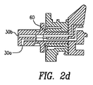
[0022]上述の実施形態の実施に適切な装置は、米国特許第5,482,739号や米国特許第6,159,866号に記載され、これらの双方の開示内容全体は本明細書に援用されている。ここで図2aを参照すると、ガス入口コンジットは、好ましくは、専用エッチャントガスフィードライン30aと別々の水素とシリコン含有ガスフィードライン30bを備える。フィードライン30aと30bは、堆積ゾーン24に隣接したガスを混合する入口ガスマニホールド60に接続されている。堆積ゾーン24に隣接したガスを混合すると、不適合性反応性ガスの早期反応が制限される。堆積ゾーンでのみ不適合性ガスの反応を可能にする好ましいガス入口の限定されない例を、図2b-図2eに示す。
[0022] Suitable devices for implementing the above-described embodiments are described in US Pat. No. 5,482,739 and US Pat. No. 6,159,866, the entire disclosure of both of which are hereby incorporated by reference. Has been incorporated. Referring now to FIG. 2a, the gas inlet conduit preferably comprises a dedicated etchant
[0023]既知のCVD膜の種類と選択的CVDに適切な堆積とエッチング化学の限定されない例を下記表1に示す。本発明の実施形態として、堆積化学とエッチング化学の一部は不適合性であるが、ウエハの付近でのみ混合するように意図的に選ばれる。 [0023] Non-limiting examples of known CVD film types and deposition and etch chemistries suitable for selective CVD are shown in Table 1 below. As an embodiment of the present invention, some of the deposition chemistry and etching chemistry are incompatible, but are intentionally chosen to mix only near the wafer.

[0024]特に、発明の実施形態は、単一ウエハランプ加熱熱反応チャンバ、例えば、図1に記載されたチャンバ内で水素含有ガス及び/又はシリコン含有ガスと、強力な酸化又はエッチング化学物質、例えば、塩素、臭素、フッ素、又はヨウ素とを混合又は反応させるために用いられる方法及び装置に関する。例えば、Cl2+SiH4の反応は、励起状態で寿命の短いSiClxとHClを生じる。このような方法と反応チャンバは、種々の膜形成プロセスに、例えば、シリコン含有膜、ゲルマニウム含有膜、又は炭素含有膜(又はこれらの組み合わせ)膜の堆積又はこのようなプロセス後のインサイチュ熱チャンバ洗浄に使用し得る。これらの膜は、ホウ素、ヒ素、リン又は他の適切なp形又はn形のドーパントでドープされてもドープされなくてもよく、これらは先端的デバイスの形成に技術的に重要である。 [0024] In particular, embodiments of the invention include a single wafer lamp heated thermal reaction chamber, such as a hydrogen-containing gas and / or a silicon-containing gas and a powerful oxidizing or etching chemistry in the chamber described in FIG. For example, it relates to a method and apparatus used for mixing or reacting chlorine, bromine, fluorine, or iodine. For example, the reaction of Cl 2 + SiH 4 produces SiCl x and HCl that have a short lifetime in the excited state. Such methods and reaction chambers are useful for various film formation processes, such as deposition of silicon-containing films, germanium-containing films, or carbon-containing films (or combinations thereof) or in-situ thermal chamber cleaning after such processes. Can be used for These films may or may not be doped with boron, arsenic, phosphorous or other suitable p-type or n-type dopants, which are technically important for the formation of advanced devices.
[0025]一つ以上の実施形態において、水素含有ガス(独立したソースガスとして又はある前駆化合物を持つキャリヤガスとして)は、制御された条件下で分子エッチング化学物質(例えば、Cl2、F2、Br2、又はI2)と反応チャンバへ同時に噴射されて、ウエハ表面に隣接して準安定化学種を形成する。成長とエッチングの反応経路で著しく変動する種々の準安定化学種が生成され得る。例えば、本発明の実施形態によれば、水素含有ガスをウエハ表面に隣接して200℃を超える温度で減圧(例えば、200トール未満)において塩素と種々の組成(0%水素〜100%の水素、混合物の残りは塩素)で混合して、堆積やエッチングのような種々のプロセスに使用し得る準安定化学種を形成する。 [0025] In one or more embodiments, a hydrogen-containing gas (as an independent source gas or as a carrier gas with some precursor compound) is controlled by molecular etching chemistries (eg, Cl 2 , F 2 ) under controlled conditions. , Br 2 , or I 2 ) and the reaction chamber at the same time to form a metastable species adjacent to the wafer surface. Various metastable species can be generated that vary significantly in the growth and etch reaction paths. For example, according to embodiments of the present invention, the hydrogen-containing gas is adjacent to the wafer surface at a temperature above 200 ° C. at reduced pressure (eg, less than 200 Torr) with chlorine and various compositions (0% hydrogen to 100% hydrogen). The remainder of the mixture is mixed with chlorine) to form metastable species that can be used in various processes such as deposition and etching.
[0026]水素含有ガスとエッチングガスの反応は、反応が準安定化学種を形成させるのに充分な温度にウエハを加熱することによって低圧で開始され又は触媒される。加熱したウエハが反応の開始源として用いられることから、準安定化学種反応は低圧でウエハ表面に近接してのみ生じる。反応種ガス濃度と分圧は、チャンバ内で自然の完全な反応を防止するように制御される。反応中、所定値以下で反応種ガス混合物のチャンバの分圧を保つことによって、いかなる反応種ガス濃度も、望まない再結合が完了する前にウエハ上に膜成長とエッチング用の準安定化学種を形成するために用いることができる。 [0026] The reaction between the hydrogen-containing gas and the etching gas is initiated or catalyzed at low pressure by heating the wafer to a temperature sufficient for the reaction to form a metastable species. Because the heated wafer is used as the reaction source, the metastable species reaction only occurs close to the wafer surface at low pressure. The reactant gas concentration and partial pressure are controlled to prevent a natural complete reaction in the chamber. By maintaining the chamber partial pressure of the reactant gas mixture below a predetermined value during the reaction, any reactant gas concentration can be adjusted so that any metastable species for film growth and etching on the wafer before unwanted recombination is complete. Can be used to form
[0027]特に準安定化学種でエッチングすることを含むプロセスに関する実施形態において、少なくとも二つの方法がエッチング濃度を調節のために使用し得る。一実施形態によれば、水素とエッチングガス、例えば、塩素の相対的組成が調整される。他の実施形態において、組成物は、エッチングプロセスを制御するために、追加の不活性ガス、例えば、窒素又はアルゴンを噴射することによって希釈され得る。更に、プロセス圧と流量は調節を可能にするように変更され得る。 [0027] In embodiments involving processes that include etching with metastable species in particular, at least two methods may be used to adjust the etch concentration. According to one embodiment, the relative composition of hydrogen and an etching gas, such as chlorine, is adjusted. In other embodiments, the composition can be diluted by injecting additional inert gas, such as nitrogen or argon, to control the etching process. Furthermore, the process pressure and flow rate can be varied to allow adjustment.
[0028]図3は、プロセスガスの割合を調整する影響及びシリコン堆積速度に対する影響を示すグラフである。図3は、六つの異なるプロセス条件に対する標準化シリコン堆積速度のグラフである。図3のデータ点の各々は、各データ点の下に指定される以外、シリコン膜の堆積のための標準堆積条件を用いてAppliedMaterials Epi Rp Centura(登録商標)リアクタで作成した。各データ点について、プロセスガスの割合及び/又は組成は、堆積速度に対する影響を求めるように調整した。図3のデータ点1-4については、堆積は、約620℃の温度、10トールの圧力で水素キャリヤガスを用いて行った。シリコン源ガスは、各データ点について同一にした。データ点1については、水素と塩素とシリコンの流量は15.4:0:0.0025であった。データ点2については、塩素と水素ガスは、データ点1での条件を用いて形成された膜をエッチングするために基板に隣接して導入した。データ点2については、エッチングの間の水素と塩素とシリコン源ガスの流量は、15:0.001:0にした。条件3については、データ点1のプロセス条件を用いて形成された膜をエッチングするために塩素と窒素を用いた。データ点3では、水素と塩素とシリコンガスの割合は、0:0.01:0とした。条件4では、データ点1で流した堆積ガスと共に塩素を流した。データ点4における水素と塩素とシリコン源ガスの割合は、15.4:0.01:0.0025であった。
[0028] FIG. 3 is a graph illustrating the effect of adjusting the proportion of process gas and the effect on silicon deposition rate. FIG. 3 is a graph of normalized silicon deposition rates for six different process conditions. Each of the data points in FIG. 3 was created in an Applied Materials Epi Rp Centura® reactor using standard deposition conditions for silicon film deposition, except as specified below each data point. For each data point, the ratio and / or composition of process gas was adjusted to determine the effect on the deposition rate. For data points 1-4 in FIG. 3, deposition was performed using a hydrogen carrier gas at a temperature of about 620 ° C. and a pressure of 10 Torr. The silicon source gas was the same for each data point. For
[0029]データ点5と6については、約570℃の温度と10トールの圧力で窒素キャリヤガス中で堆積を行った。データ点5については、水素と塩素とシリコン源ガスを0.4:0:0.0025の流量比でシリコン膜を堆積した。データ点6では、水素と塩素とシリコン源ガス0.4:0.0015:0.0025の流量比でデータ点5を作成するために用いた堆積ガスと塩素を同時に流した。これらのデータ点が単なる例示であり、広い範囲の流量比、温度、圧力、他の態様が本発明の範囲内であることを当業者が容易に理解することは当然のことである。図3に示したデータは、シリコンの堆積流量に対するプロセスガスの流量比の変化の影響を示すグラフである。
[0029] Data points 5 and 6 were deposited in nitrogen carrier gas at a temperature of about 570 ° C. and a pressure of 10 Torr. For
[0030]不適合性化学物質間の反応は、単一ウエハランプ加熱熱反応チャンバ内で制御することができ、その場合、内部表面温度とウエハ温度は急速な調節を受けることができる。温度がフィードガスを破壊又は分解するのに充分でないような冷却条件下でリアクタにガスを供給するこのような単一ウエハリアクタは、準安定化学種がウエハ表面に隣接して又はウエハ表面でリアクタの内部で生成され得る点で可撓性を与える。従って、本発明の準安定化学種生成反応は、ウエハの加熱した表面が反応を起こさせるのに必要であるが、準安定化学種を形成する反応には消費されないことから、“表面触媒”と呼ばれる。 [0030] The reaction between incompatible chemicals can be controlled in a single wafer lamp heated thermal reaction chamber, in which case the internal surface temperature and wafer temperature can be subject to rapid adjustment. Such single wafer reactors that supply gas to the reactor under cooling conditions where the temperature is not sufficient to destroy or decompose the feed gas are those in which metastable species are adjacent to or at the wafer surface. It provides flexibility in that it can be generated inside. Therefore, the metastable species generation reaction of the present invention is necessary for the heated surface of the wafer to cause the reaction, but it is not consumed in the reaction to form the metastable species, so that “surface catalyst” be called.
[0031]更に、加熱するためにランプを用いる急速に加熱したリアクタにおいて、準安定化学種を形成する反応は、ウエハ温度とリアクタ内の他の加熱した表面、例えば、サセプタ、ライナ又はドームを上げたり下げたりすることによって急速に制御され得る。このことは、強度だけでなく、これらの反応の開始と終了を調節する都合の良い方法である。ランプ加熱によっても、これらの反応を調節するエネルギーが追加され、一部はランプが供給する熱エネルギーに加えて感光性がある。ランプ放熱は、紫外ランプ(UV又はVUV範囲100-400nm波長)だけでなく赤外ランプに及ぶ種々のランプによって供給され得る。UV放熱は、分子エッチング化学がより低温で、同様の利点を得る水素が少ないか又は全く含まずに分解され得る点で更に有利である。 [0031] In addition, in rapidly heated reactors that use lamps to heat, reactions that form metastable species increase wafer temperature and other heated surfaces in the reactor, such as susceptors, liners, or domes. It can be controlled quickly by lowering or lowering. This is a convenient way to control not only the intensity but also the onset and termination of these reactions. Lamp heating also adds energy to regulate these reactions, and some are photosensitive in addition to the thermal energy supplied by the lamp. Lamp heat dissipation can be supplied by various lamps ranging from infrared lamps as well as ultraviolet lamps (UV or VUV range 100-400 nm wavelength). UV heat dissipation is further advantageous in that the molecular etch chemistry can be decomposed at lower temperatures and with little or no hydrogen to obtain similar benefits.
[0032]本発明を本明細書では具体的な実施形態によって記載してきたが、これらの実施形態は本発明の原理と適用を単に例示していることは理解すべきである。種々の修正や変更が、発明の精神と範囲から逸脱せずに本発明の方法を行うことができることは当業者に明らかである。従って、本発明には、添付の特許請求の範囲の範囲内である修正や変更、また、これらの等価物が含まれることを意味する。 [0032] While the invention herein has been described by specific embodiments, it is to be understood that these embodiments are merely illustrative of the principles and applications of the present invention. It will be apparent to those skilled in the art that various modifications and variations can be made in the method of the present invention without departing from the spirit and scope of the invention. Thus, it is intended that the present invention include modifications and variations that are within the scope of the appended claims, and equivalents thereof.
10…装置、20…ハウジング、22…堆積チャンバ、23…囲壁、24…堆積ゾーン、26…ホルダー、28…基板、29…ドライブアセンブリ、30…入口ガスコンジット、30a…フィードライン、30b…フィードライン、32…ガス排出コンジット、40…ヒータ、41…石英ドーム、60…入口ガスモニホールド、70…排出マニホールド、72…排出ライン、74…遮断弁、76…圧力制御バルブ。
DESCRIPTION OF
Claims (15)
該反応チャンバに水素含有ガスを導入するステップと;
該水素含有ガスから隔離された別のコンジット内にある、該水素含有ガスと自然反応するエッチング化学物質を、該反応チャンバに導入し、該水素含有ガスと該エッチング化学物質との反応種ガス濃度をもたらすステップと;
1つ以上の反応条件を制御することにより該水素含有ガスと該エッチング化学物質との自然反応を防ぐステップと;
該反応条件のうちの1つ以上の反応条件を調節し、制御された反応条件のもとで、該水素含有ガスと該エッチング化学物質を該ウエハの表面に隣接した領域で反応させて、該ウエハの表面に隣接して準安定化学種を形成するステップと;
該準安定化学種をその後の成長又はエッチング反応に使用するステップと;
を含み、
該反応条件のうちの1つ以上の反応条件は、分圧、反応種ガス濃度及びそれらの組み合わせからなる群から選択される前記方法。 A method of processing a wafer during a film formation process in a reaction chamber comprising:
Introducing a hydrogen-containing gas into the reaction chamber;
An etching chemical that spontaneously reacts with the hydrogen-containing gas in a separate conduit that is isolated from the hydrogen-containing gas is introduced into the reaction chamber, and a reactive species gas concentration of the hydrogen-containing gas and the etching chemical is introduced. Steps to bring about;
Preventing spontaneous reaction between the hydrogen-containing gas and the etching chemical by controlling one or more reaction conditions;
Adjusting one or more of the reaction conditions and reacting the hydrogen-containing gas and the etch chemistry in a region adjacent to the surface of the wafer under controlled reaction conditions, Forming a metastable species adjacent to the surface of the wafer;
A method for use in a subsequent growth or etching reacting the metastable species;
Including
One or more of the reaction conditions is selected from the group consisting of partial pressure , reactant gas concentration, and combinations thereof.
該ウエハ表面に隣接した別々のコンジットに自然反応性化学物質を送出し、反応種濃度をもたらすステップと;
分圧、反応種濃度及びそれらの組み合わせからなる群から選択される、1つ以上の反応条件を制御し、該自然反応性物質の自然反応を防ぐステップと;
分圧、温度、反応種濃度及びそれらの組み合わせからなる群から選択される、該反応条件のうちの1つ以上の反応条件を調節し、制御された条件のもとで、該化学物質を、該ウエハ表面に隣接した領域で反応させて準安定化学種を形成するステップと;
該準安定化学種をその後の反応に用いるステップと;
を含む、前記方法。 A method of processing a wafer during a film formation process in a reaction chamber comprising:
Delivering spontaneously reactive chemicals to separate conduits adjacent to the wafer surface to provide reactive species concentrations;
Controlling one or more reaction conditions selected from the group consisting of partial pressure , reactive species concentration and combinations thereof, to prevent spontaneous reaction of the naturally reactive substance;
Adjusting one or more of the reaction conditions selected from the group consisting of partial pressure, temperature, reactive species concentration and combinations thereof, and under controlled conditions, Reacting in a region adjacent to the wafer surface to form a metastable species ;
A step of using the metastable species in subsequent reactions;
Said method.
該ウエハの温度を約700℃未満に維持するステップと;
該ウエハ表面に隣接してCl2とシランを混合して、該ウエハ表面に隣接してSiClx中間体を形成するステップと;
該ウエハ表面上に膜を堆積させるステップと;
を含む、前記方法。 A method of processing a film on a wafer during a film formation process in a reaction chamber comprising:
Maintaining the temperature of the wafer below about 700 ° C .;
Mixing Cl 2 and silane adjacent to the wafer surface to form an SiCl x intermediate adjacent to the wafer surface;
Depositing a film on the wafer surface;
Said method.
Applications Claiming Priority (3)
| Application Number | Priority Date | Filing Date | Title |
|---|---|---|---|
| US11/336,178 US7709391B2 (en) | 2006-01-20 | 2006-01-20 | Methods for in-situ generation of reactive etch and growth specie in film formation processes |
| US11/336,178 | 2006-01-20 | ||
| PCT/US2007/000338 WO2008127220A2 (en) | 2006-01-20 | 2007-01-09 | Methods for in-situ generation of reactive etch and growth specie in film formation processes |
Publications (3)
| Publication Number | Publication Date |
|---|---|
| JP2009531872A JP2009531872A (en) | 2009-09-03 |
| JP2009531872A5 JP2009531872A5 (en) | 2010-02-12 |
| JP5420397B2 true JP5420397B2 (en) | 2014-02-19 |
Family
ID=38284511
Family Applications (1)
| Application Number | Title | Priority Date | Filing Date |
|---|---|---|---|
| JP2009509546A Expired - Fee Related JP5420397B2 (en) | 2006-01-20 | 2007-01-09 | A method for in situ generation of reactive etching and growth species in a film formation process |
Country Status (5)
| Country | Link |
|---|---|
| US (1) | US7709391B2 (en) |
| JP (1) | JP5420397B2 (en) |
| KR (2) | KR101237868B1 (en) |
| TW (1) | TWI379346B (en) |
| WO (1) | WO2008127220A2 (en) |
Families Citing this family (21)
| Publication number | Priority date | Publication date | Assignee | Title |
|---|---|---|---|---|
| US20090087967A1 (en) * | 2005-11-14 | 2009-04-02 | Todd Michael A | Precursors and processes for low temperature selective epitaxial growth |
| US20080070356A1 (en) * | 2006-09-14 | 2008-03-20 | Advanced Micro Devices, Inc. | Trench replacement gate process for transistors having elevated source and drain regions |
| US7976634B2 (en) * | 2006-11-21 | 2011-07-12 | Applied Materials, Inc. | Independent radiant gas preheating for precursor disassociation control and gas reaction kinetics in low temperature CVD systems |
| WO2009136974A2 (en) * | 2008-02-07 | 2009-11-12 | Los Alamos National Security, Llc | Thick-shell nanocrystal quantum dots |
| KR101064873B1 (en) * | 2009-10-23 | 2011-09-16 | 주성엔지니어링(주) | Substrate Processing Apparatus and Method |
| WO2012067112A1 (en) | 2010-11-17 | 2012-05-24 | 新日本製鐵株式会社 | Method for producing epitaxial silicon carbide single crystal substrate |
| JP5837178B2 (en) * | 2011-03-22 | 2015-12-24 | アプライド マテリアルズ インコーポレイテッドApplied Materials,Incorporated | Liner assembly for chemical vapor deposition chambers |
| US9499905B2 (en) * | 2011-07-22 | 2016-11-22 | Applied Materials, Inc. | Methods and apparatus for the deposition of materials on a substrate |
| JP5876398B2 (en) * | 2012-10-18 | 2016-03-02 | 東京エレクトロン株式会社 | Film forming method and film forming apparatus |
| US20140116336A1 (en) * | 2012-10-26 | 2014-05-01 | Applied Materials, Inc. | Substrate process chamber exhaust |
| US11414759B2 (en) * | 2013-11-29 | 2022-08-16 | Taiwan Semiconductor Manufacturing Co., Ltd | Mechanisms for supplying process gas into wafer process apparatus |
| KR102150728B1 (en) * | 2013-12-16 | 2020-09-01 | 에스케이실트론 주식회사 | Apparatus and Method for Cleaning Process Chamber |
| KR102705337B1 (en) | 2015-12-04 | 2024-09-11 | 어플라이드 머티어리얼스, 인코포레이티드 | Methods and solutions for cleaning InGaAs (or III-V) substrates |
| KR102408720B1 (en) | 2017-06-07 | 2022-06-14 | 삼성전자주식회사 | Semiconductor process chamber including upper dome |
| JP6971823B2 (en) * | 2017-12-13 | 2021-11-24 | 東京エレクトロン株式会社 | Etching method for silicon-containing film, computer storage medium, and etching device for silicon-containing film |
| WO2020046567A1 (en) | 2018-08-29 | 2020-03-05 | Applied Materials, Inc. | Chamber injector |
| US11257671B2 (en) * | 2018-09-28 | 2022-02-22 | Taiwan Semiconductor Manufacturing Co., Ltd. | Method and system of control of epitaxial growth |
| FI128855B (en) * | 2019-09-24 | 2021-01-29 | Picosun Oy | Fluid distributing device for a thin-film deposition apparatus, related apparatus and methods |
| TWI749521B (en) * | 2020-04-13 | 2021-12-11 | 大陸商蘇州雨竹機電有限公司 | Multi-channel gas ejector with series cooling chamber |
| US20220290293A1 (en) * | 2021-03-15 | 2022-09-15 | HelioSource Tech, LLC | Hardware and processes for in operando deposition shield replacement/surface cleaning |
| CN119889750B (en) * | 2025-01-13 | 2025-11-28 | 西北工业大学 | Prismatic TRISO particle dispersion additive fuel element and preparation method and application thereof |
Family Cites Families (22)
| Publication number | Priority date | Publication date | Assignee | Title |
|---|---|---|---|---|
| US4613400A (en) | 1985-05-20 | 1986-09-23 | Applied Materials, Inc. | In-situ photoresist capping process for plasma etching |
| US4963506A (en) * | 1989-04-24 | 1990-10-16 | Motorola Inc. | Selective deposition of amorphous and polycrystalline silicon |
| US5108792A (en) | 1990-03-09 | 1992-04-28 | Applied Materials, Inc. | Double-dome reactor for semiconductor processing |
| US5179677A (en) | 1990-08-16 | 1993-01-12 | Applied Materials, Inc. | Apparatus and method for substrate heating utilizing various infrared means to achieve uniform intensity |
| JP3149464B2 (en) * | 1991-06-28 | 2001-03-26 | 日本電気株式会社 | Method and apparatus for selective growth of silicon epitaxial film |
| US5916369A (en) | 1995-06-07 | 1999-06-29 | Applied Materials, Inc. | Gas inlets for wafer processing chamber |
| DE69421463T2 (en) * | 1993-07-30 | 2000-02-10 | Applied Materials, Inc. | Deposit of silicon nitride |
| DE69433656T2 (en) * | 1993-07-30 | 2005-02-17 | Applied Materials, Inc., Santa Clara | A method of introducing reactive gas into a substrate processing apparatus |
| JP3761918B2 (en) * | 1994-09-13 | 2006-03-29 | 株式会社東芝 | Manufacturing method of semiconductor device |
| JP3725598B2 (en) * | 1996-01-12 | 2005-12-14 | 東芝セラミックス株式会社 | Epitaxial wafer manufacturing method |
| US6011031A (en) * | 1997-05-30 | 2000-01-04 | Dr. Reddy's Research Foundation | Azolidinediones useful for the treatment of diabetes, dyslipidemia and hypertension: process for their preparation and pharmaceutical compositions containing them |
| US6037273A (en) | 1997-07-11 | 2000-03-14 | Applied Materials, Inc. | Method and apparatus for insitu vapor generation |
| US6159866A (en) | 1998-03-02 | 2000-12-12 | Applied Materials, Inc. | Method for insitu vapor generation for forming an oxide on a substrate |
| US6951827B2 (en) * | 2000-03-15 | 2005-10-04 | Tufts University | Controlling surface chemistry on solid substrates |
| US6900133B2 (en) | 2002-09-18 | 2005-05-31 | Applied Materials, Inc | Method of etching variable depth features in a crystalline substrate |
| US6972228B2 (en) * | 2003-03-12 | 2005-12-06 | Intel Corporation | Method of forming an element of a microelectronic circuit |
| US7107820B2 (en) * | 2003-05-02 | 2006-09-19 | Praxair S.T. Technology, Inc. | Integrated gas supply and leak detection system |
| US7166528B2 (en) | 2003-10-10 | 2007-01-23 | Applied Materials, Inc. | Methods of selective deposition of heavily doped epitaxial SiGe |
| US7132338B2 (en) | 2003-10-10 | 2006-11-07 | Applied Materials, Inc. | Methods to fabricate MOSFET devices using selective deposition process |
| US7396743B2 (en) | 2004-06-10 | 2008-07-08 | Singh Kaushal K | Low temperature epitaxial growth of silicon-containing films using UV radiation |
| DE102004061036B4 (en) * | 2004-12-18 | 2008-10-30 | Daimler Ag | Windbreak for convertibles |
| US7816236B2 (en) * | 2005-02-04 | 2010-10-19 | Asm America Inc. | Selective deposition of silicon-containing films |
-
2006
- 2006-01-20 US US11/336,178 patent/US7709391B2/en not_active Expired - Lifetime
-
2007
- 2007-01-09 WO PCT/US2007/000338 patent/WO2008127220A2/en not_active Ceased
- 2007-01-09 KR KR1020117000355A patent/KR101237868B1/en not_active Expired - Fee Related
- 2007-01-09 KR KR1020087020262A patent/KR101024194B1/en not_active Expired - Fee Related
- 2007-01-09 JP JP2009509546A patent/JP5420397B2/en not_active Expired - Fee Related
- 2007-01-19 TW TW096102220A patent/TWI379346B/en not_active IP Right Cessation
Also Published As
| Publication number | Publication date |
|---|---|
| US7709391B2 (en) | 2010-05-04 |
| JP2009531872A (en) | 2009-09-03 |
| WO2008127220A2 (en) | 2008-10-23 |
| KR20110023880A (en) | 2011-03-08 |
| KR101237868B1 (en) | 2013-03-04 |
| WO2008127220A3 (en) | 2009-04-16 |
| KR20090012206A (en) | 2009-02-02 |
| TWI379346B (en) | 2012-12-11 |
| US20070170148A1 (en) | 2007-07-26 |
| KR101024194B1 (en) | 2011-03-22 |
| TW200729304A (en) | 2007-08-01 |
Similar Documents
| Publication | Publication Date | Title |
|---|---|---|
| JP5420397B2 (en) | A method for in situ generation of reactive etching and growth species in a film formation process | |
| US7262116B2 (en) | Low temperature epitaxial growth of silicon-containing films using close proximity UV radiation | |
| US7629267B2 (en) | High stress nitride film and method for formation thereof | |
| KR101975071B1 (en) | Plasma activated conformal dielectric film deposition | |
| US20090087967A1 (en) | Precursors and processes for low temperature selective epitaxial growth | |
| US20060286774A1 (en) | Method for forming silicon-containing materials during a photoexcitation deposition process | |
| US7029995B2 (en) | Methods for depositing amorphous materials and using them as templates for epitaxial films by solid phase epitaxy | |
| US20100018460A1 (en) | Method for forming silicon-containing materials during a photoexcitation deposition process | |
| US7897491B2 (en) | Separate injection of reactive species in selective formation of films | |
| JP2009521801A (en) | Epitaxial deposition of doped semiconductor materials. | |
| TW201323647A (en) | Atomic layer deposition using a film containing a precursor of yttrium or zirconium | |
| KR20120023040A (en) | Method of forming in-situ pre-gan deposition layer in hvpe | |
| JPH06252057A (en) | Manufacture of semiconductor device | |
| WO2010129289A2 (en) | Decontamination of mocvd chamber using nh3 purge after in-situ cleaning | |
| US20260047358A1 (en) | High growth rate selective si:p process | |
| KR101176668B1 (en) | Low temperature epitaxial growth of silicon-containing films using uv radiation | |
| US20260060016A1 (en) | Substrate processing including initial etching and fast etching, and related methods, apparatus, systems, and chambers | |
| CN120967508A (en) | Growth method of silicon carbide epitaxial wafer and silicon carbide epitaxial wafer |
Legal Events
| Date | Code | Title | Description |
|---|---|---|---|
| A521 | Request for written amendment filed |
Free format text: JAPANESE INTERMEDIATE CODE: A523 Effective date: 20091211 |
|
| A621 | Written request for application examination |
Free format text: JAPANESE INTERMEDIATE CODE: A621 Effective date: 20091211 |
|
| A977 | Report on retrieval |
Free format text: JAPANESE INTERMEDIATE CODE: A971007 Effective date: 20100628 |
|
| RD03 | Notification of appointment of power of attorney |
Free format text: JAPANESE INTERMEDIATE CODE: A7423 Effective date: 20101130 |
|
| RD04 | Notification of resignation of power of attorney |
Free format text: JAPANESE INTERMEDIATE CODE: A7424 Effective date: 20101210 |
|
| A131 | Notification of reasons for refusal |
Free format text: JAPANESE INTERMEDIATE CODE: A131 Effective date: 20120221 |
|
| A521 | Request for written amendment filed |
Free format text: JAPANESE INTERMEDIATE CODE: A523 Effective date: 20120518 |
|
| A131 | Notification of reasons for refusal |
Free format text: JAPANESE INTERMEDIATE CODE: A131 Effective date: 20120731 |
|
| RD04 | Notification of resignation of power of attorney |
Free format text: JAPANESE INTERMEDIATE CODE: A7424 Effective date: 20120925 |
|
| A601 | Written request for extension of time |
Free format text: JAPANESE INTERMEDIATE CODE: A601 Effective date: 20121029 |
|
| A602 | Written permission of extension of time |
Free format text: JAPANESE INTERMEDIATE CODE: A602 Effective date: 20121105 |
|
| A521 | Request for written amendment filed |
Free format text: JAPANESE INTERMEDIATE CODE: A523 Effective date: 20121129 |
|
| A131 | Notification of reasons for refusal |
Free format text: JAPANESE INTERMEDIATE CODE: A131 Effective date: 20130312 |
|
| A601 | Written request for extension of time |
Free format text: JAPANESE INTERMEDIATE CODE: A601 Effective date: 20130611 |
|
| A602 | Written permission of extension of time |
Free format text: JAPANESE INTERMEDIATE CODE: A602 Effective date: 20130618 |
|
| A521 | Request for written amendment filed |
Free format text: JAPANESE INTERMEDIATE CODE: A523 Effective date: 20130628 |
|
| A01 | Written decision to grant a patent or to grant a registration (utility model) |
Free format text: JAPANESE INTERMEDIATE CODE: A01 Effective date: 20131112 |
|
| A61 | First payment of annual fees (during grant procedure) |
Free format text: JAPANESE INTERMEDIATE CODE: A61 Effective date: 20131120 |
|
| LAPS | Cancellation because of no payment of annual fees |