JP5410974B2 - Nonvolatile nanotube diode, nonvolatile nanotube block, system using the same, and manufacturing method thereof - Google Patents
Nonvolatile nanotube diode, nonvolatile nanotube block, system using the same, and manufacturing method thereof Download PDFInfo
- Publication number
- JP5410974B2 JP5410974B2 JP2009523981A JP2009523981A JP5410974B2 JP 5410974 B2 JP5410974 B2 JP 5410974B2 JP 2009523981 A JP2009523981 A JP 2009523981A JP 2009523981 A JP2009523981 A JP 2009523981A JP 5410974 B2 JP5410974 B2 JP 5410974B2
- Authority
- JP
- Japan
- Prior art keywords
- nanotube
- diode
- volatile
- terminal
- conductive
- Prior art date
- Legal status (The legal status is an assumption and is not a legal conclusion. Google has not performed a legal analysis and makes no representation as to the accuracy of the status listed.)
- Active
Links
- 239000002071 nanotube Substances 0.000 title claims description 1478
- 238000004519 manufacturing process Methods 0.000 title description 265
- 239000004065 semiconductor Substances 0.000 claims description 227
- 239000004020 conductor Substances 0.000 claims description 205
- 239000000463 material Substances 0.000 claims description 162
- 239000004744 fabric Substances 0.000 claims description 136
- 239000000758 substrate Substances 0.000 claims description 114
- 230000000638 stimulation Effects 0.000 claims description 67
- -1 RbSi 2 Inorganic materials 0.000 claims description 60
- 229910052782 aluminium Inorganic materials 0.000 claims description 58
- 229910052721 tungsten Inorganic materials 0.000 claims description 47
- 229910052802 copper Inorganic materials 0.000 claims description 42
- 229910052763 palladium Inorganic materials 0.000 claims description 41
- 229910052804 chromium Inorganic materials 0.000 claims description 40
- 229910019001 CoSi Inorganic materials 0.000 claims description 39
- 229910052741 iridium Inorganic materials 0.000 claims description 39
- 229910052709 silver Inorganic materials 0.000 claims description 39
- 229910008484 TiSi Inorganic materials 0.000 claims description 38
- 229910052697 platinum Inorganic materials 0.000 claims description 24
- 239000010405 anode material Substances 0.000 claims description 22
- 230000004044 response Effects 0.000 claims description 22
- 230000005669 field effect Effects 0.000 claims description 14
- VLJQDHDVZJXNQL-UHFFFAOYSA-N 4-methyl-n-(oxomethylidene)benzenesulfonamide Chemical compound CC1=CC=C(S(=O)(=O)N=C=O)C=C1 VLJQDHDVZJXNQL-UHFFFAOYSA-N 0.000 claims description 13
- 229910016006 MoSi Inorganic materials 0.000 claims description 13
- 229910006249 ZrSi Inorganic materials 0.000 claims description 13
- 230000004888 barrier function Effects 0.000 claims description 13
- 229910052742 iron Inorganic materials 0.000 claims description 13
- 229910021340 platinum monosilicide Inorganic materials 0.000 claims description 13
- 238000004891 communication Methods 0.000 claims description 12
- 229910052701 rubidium Inorganic materials 0.000 claims description 12
- 229910052725 zinc Inorganic materials 0.000 claims description 11
- 239000004745 nonwoven fabric Substances 0.000 claims 1
- 238000000034 method Methods 0.000 description 826
- 210000004027 cell Anatomy 0.000 description 732
- 239000010410 layer Substances 0.000 description 678
- 239000012212 insulator Substances 0.000 description 512
- 230000015654 memory Effects 0.000 description 504
- 229910021420 polycrystalline silicon Inorganic materials 0.000 description 267
- 229920005591 polysilicon Polymers 0.000 description 265
- 238000005530 etching Methods 0.000 description 97
- 229910052751 metal Inorganic materials 0.000 description 96
- 239000002184 metal Substances 0.000 description 96
- 230000008569 process Effects 0.000 description 84
- 238000000151 deposition Methods 0.000 description 73
- 238000005516 engineering process Methods 0.000 description 70
- 238000003491 array Methods 0.000 description 57
- 229910052718 tin Inorganic materials 0.000 description 57
- 230000000873 masking effect Effects 0.000 description 51
- 238000001020 plasma etching Methods 0.000 description 48
- 229910021332 silicide Inorganic materials 0.000 description 44
- 239000011521 glass Substances 0.000 description 39
- 239000003989 dielectric material Substances 0.000 description 38
- 150000002739 metals Chemical class 0.000 description 37
- 229910052737 gold Inorganic materials 0.000 description 35
- 238000003860 storage Methods 0.000 description 35
- 229910052750 molybdenum Inorganic materials 0.000 description 34
- 230000001681 protective effect Effects 0.000 description 32
- 239000013078 crystal Substances 0.000 description 31
- 229910018072 Al 2 O 3 Inorganic materials 0.000 description 30
- ATJFFYVFTNAWJD-UHFFFAOYSA-N Tin Chemical compound [Sn] ATJFFYVFTNAWJD-UHFFFAOYSA-N 0.000 description 30
- 239000002019 doping agent Substances 0.000 description 30
- 239000002048 multi walled nanotube Substances 0.000 description 30
- 229910004298 SiO 2 Inorganic materials 0.000 description 29
- 229910052738 indium Inorganic materials 0.000 description 29
- 230000002829 reductive effect Effects 0.000 description 29
- 229920000642 polymer Polymers 0.000 description 28
- 230000015572 biosynthetic process Effects 0.000 description 27
- 229910052759 nickel Inorganic materials 0.000 description 27
- 229910019899 RuO Inorganic materials 0.000 description 26
- 229910004166 TaN Inorganic materials 0.000 description 26
- 229910010165 TiCu Inorganic materials 0.000 description 26
- 229910052785 arsenic Inorganic materials 0.000 description 26
- RQNWIZPPADIBDY-UHFFFAOYSA-N arsenic atom Chemical compound [As] RQNWIZPPADIBDY-UHFFFAOYSA-N 0.000 description 26
- 229910052745 lead Inorganic materials 0.000 description 26
- 150000004767 nitrides Chemical class 0.000 description 26
- 229910052719 titanium Inorganic materials 0.000 description 26
- 229910001258 titanium gold Inorganic materials 0.000 description 26
- 239000002033 PVDF binder Substances 0.000 description 25
- 238000002955 isolation Methods 0.000 description 25
- 229910052698 phosphorus Inorganic materials 0.000 description 25
- BASFCYQUMIYNBI-UHFFFAOYSA-N platinum Chemical compound [Pt] BASFCYQUMIYNBI-UHFFFAOYSA-N 0.000 description 25
- OAICVXFJPJFONN-UHFFFAOYSA-N Phosphorus Chemical compound [P] OAICVXFJPJFONN-UHFFFAOYSA-N 0.000 description 24
- 239000011574 phosphorus Substances 0.000 description 24
- BOTDANWDWHJENH-UHFFFAOYSA-N Tetraethyl orthosilicate Chemical compound CCO[Si](OCC)(OCC)OCC BOTDANWDWHJENH-UHFFFAOYSA-N 0.000 description 23
- 230000008021 deposition Effects 0.000 description 23
- 238000010586 diagram Methods 0.000 description 23
- 229910001092 metal group alloy Inorganic materials 0.000 description 23
- 238000011049 filling Methods 0.000 description 22
- 239000005360 phosphosilicate glass Substances 0.000 description 22
- 229920000379 polypropylene carbonate Polymers 0.000 description 21
- 238000004806 packaging method and process Methods 0.000 description 19
- 239000004642 Polyimide Substances 0.000 description 18
- 229920001721 polyimide Polymers 0.000 description 18
- 125000006850 spacer group Chemical group 0.000 description 18
- 229920002981 polyvinylidene fluoride Polymers 0.000 description 17
- 229910052707 ruthenium Inorganic materials 0.000 description 17
- FVBUAEGBCNSCDD-UHFFFAOYSA-N silicide(4-) Chemical compound [Si-4] FVBUAEGBCNSCDD-UHFFFAOYSA-N 0.000 description 16
- 239000002059 nanofabric Substances 0.000 description 15
- 230000002441 reversible effect Effects 0.000 description 15
- 229910052710 silicon Inorganic materials 0.000 description 15
- 239000011800 void material Substances 0.000 description 15
- 238000013461 design Methods 0.000 description 14
- 230000001965 increasing effect Effects 0.000 description 14
- 238000000059 patterning Methods 0.000 description 14
- 229910004541 SiN Inorganic materials 0.000 description 13
- 229920002120 photoresistant polymer Polymers 0.000 description 13
- 239000010703 silicon Substances 0.000 description 13
- XUIMIQQOPSSXEZ-UHFFFAOYSA-N Silicon Chemical compound [Si] XUIMIQQOPSSXEZ-UHFFFAOYSA-N 0.000 description 12
- 239000011248 coating agent Substances 0.000 description 12
- 238000000576 coating method Methods 0.000 description 12
- 239000004593 Epoxy Substances 0.000 description 11
- LTPBRCUWZOMYOC-UHFFFAOYSA-N beryllium oxide Inorganic materials O=[Be] LTPBRCUWZOMYOC-UHFFFAOYSA-N 0.000 description 11
- 238000009792 diffusion process Methods 0.000 description 11
- 230000006870 function Effects 0.000 description 11
- 230000015556 catabolic process Effects 0.000 description 10
- 238000001514 detection method Methods 0.000 description 10
- 239000011810 insulating material Substances 0.000 description 10
- 230000009467 reduction Effects 0.000 description 10
- 238000012360 testing method Methods 0.000 description 10
- 239000000919 ceramic Substances 0.000 description 9
- 229910052731 fluorine Inorganic materials 0.000 description 8
- 230000006872 improvement Effects 0.000 description 8
- 238000005457 optimization Methods 0.000 description 8
- 229910052715 tantalum Inorganic materials 0.000 description 8
- 238000009825 accumulation Methods 0.000 description 7
- 230000008859 change Effects 0.000 description 7
- 239000006185 dispersion Substances 0.000 description 7
- 238000001704 evaporation Methods 0.000 description 7
- 229910052757 nitrogen Inorganic materials 0.000 description 7
- 229920000747 poly(lactic acid) Polymers 0.000 description 7
- 238000001878 scanning electron micrograph Methods 0.000 description 7
- QVGXLLKOCUKJST-UHFFFAOYSA-N atomic oxygen Chemical compound [O] QVGXLLKOCUKJST-UHFFFAOYSA-N 0.000 description 6
- JHIVVAPYMSGYDF-UHFFFAOYSA-N cyclohexanone Chemical compound O=C1CCCCC1 JHIVVAPYMSGYDF-UHFFFAOYSA-N 0.000 description 6
- 238000009413 insulation Methods 0.000 description 6
- 230000006386 memory function Effects 0.000 description 6
- 239000003960 organic solvent Substances 0.000 description 6
- 229910052760 oxygen Inorganic materials 0.000 description 6
- 239000001301 oxygen Substances 0.000 description 6
- 238000002161 passivation Methods 0.000 description 6
- 238000004549 pulsed laser deposition Methods 0.000 description 6
- 235000012431 wafers Nutrition 0.000 description 6
- 229920002799 BoPET Polymers 0.000 description 5
- 239000005041 Mylar™ Substances 0.000 description 5
- 230000007423 decrease Effects 0.000 description 5
- 239000010408 film Substances 0.000 description 5
- 230000000670 limiting effect Effects 0.000 description 5
- 239000011159 matrix material Substances 0.000 description 5
- 239000000203 mixture Substances 0.000 description 5
- 210000000352 storage cell Anatomy 0.000 description 5
- ZCYVEMRRCGMTRW-UHFFFAOYSA-N 7553-56-2 Chemical compound [I] ZCYVEMRRCGMTRW-UHFFFAOYSA-N 0.000 description 4
- WKBOTKDWSSQWDR-UHFFFAOYSA-N Bromine atom Chemical compound [Br] WKBOTKDWSSQWDR-UHFFFAOYSA-N 0.000 description 4
- ZAMOUSCENKQFHK-UHFFFAOYSA-N Chlorine atom Chemical compound [Cl] ZAMOUSCENKQFHK-UHFFFAOYSA-N 0.000 description 4
- PXGOKWXKJXAPGV-UHFFFAOYSA-N Fluorine Chemical compound FF PXGOKWXKJXAPGV-UHFFFAOYSA-N 0.000 description 4
- GDTBXPJZTBHREO-UHFFFAOYSA-N bromine Substances BrBr GDTBXPJZTBHREO-UHFFFAOYSA-N 0.000 description 4
- 229910052794 bromium Inorganic materials 0.000 description 4
- 229910052801 chlorine Inorganic materials 0.000 description 4
- 239000000460 chlorine Substances 0.000 description 4
- 230000001351 cycling effect Effects 0.000 description 4
- 239000012776 electronic material Substances 0.000 description 4
- 230000008020 evaporation Effects 0.000 description 4
- 239000011737 fluorine Substances 0.000 description 4
- 229910052732 germanium Inorganic materials 0.000 description 4
- 229910052740 iodine Inorganic materials 0.000 description 4
- 239000011630 iodine Substances 0.000 description 4
- 238000001459 lithography Methods 0.000 description 4
- 238000005259 measurement Methods 0.000 description 4
- 238000000206 photolithography Methods 0.000 description 4
- 230000008054 signal transmission Effects 0.000 description 4
- 239000002356 single layer Substances 0.000 description 4
- 238000012546 transfer Methods 0.000 description 4
- OKTJSMMVPCPJKN-UHFFFAOYSA-N Carbon Chemical compound [C] OKTJSMMVPCPJKN-UHFFFAOYSA-N 0.000 description 3
- 230000003213 activating effect Effects 0.000 description 3
- 238000000231 atomic layer deposition Methods 0.000 description 3
- 239000003990 capacitor Substances 0.000 description 3
- 239000002041 carbon nanotube Substances 0.000 description 3
- 230000007547 defect Effects 0.000 description 3
- GNPVGFCGXDBREM-UHFFFAOYSA-N germanium atom Chemical compound [Ge] GNPVGFCGXDBREM-UHFFFAOYSA-N 0.000 description 3
- 238000009533 lab test Methods 0.000 description 3
- 230000036961 partial effect Effects 0.000 description 3
- 239000011241 protective layer Substances 0.000 description 3
- 238000000926 separation method Methods 0.000 description 3
- 239000002904 solvent Substances 0.000 description 3
- 238000003892 spreading Methods 0.000 description 3
- 230000007480 spreading Effects 0.000 description 3
- 238000000992 sputter etching Methods 0.000 description 3
- 239000010409 thin film Substances 0.000 description 3
- OEPOKWHJYJXUGD-UHFFFAOYSA-N 2-(3-phenylmethoxyphenyl)-1,3-thiazole-4-carbaldehyde Chemical compound O=CC1=CSC(C=2C=C(OCC=3C=CC=CC=3)C=CC=2)=N1 OEPOKWHJYJXUGD-UHFFFAOYSA-N 0.000 description 2
- ZOXJGFHDIHLPTG-UHFFFAOYSA-N Boron Chemical compound [B] ZOXJGFHDIHLPTG-UHFFFAOYSA-N 0.000 description 2
- 239000002253 acid Substances 0.000 description 2
- XAGFODPZIPBFFR-UHFFFAOYSA-N aluminium Chemical compound [Al] XAGFODPZIPBFFR-UHFFFAOYSA-N 0.000 description 2
- 239000007864 aqueous solution Substances 0.000 description 2
- 239000003125 aqueous solvent Substances 0.000 description 2
- 230000006399 behavior Effects 0.000 description 2
- 230000005540 biological transmission Effects 0.000 description 2
- 229910052796 boron Inorganic materials 0.000 description 2
- 229910021393 carbon nanotube Inorganic materials 0.000 description 2
- 238000005229 chemical vapour deposition Methods 0.000 description 2
- 230000008878 coupling Effects 0.000 description 2
- 238000010168 coupling process Methods 0.000 description 2
- 238000005859 coupling reaction Methods 0.000 description 2
- 230000001419 dependent effect Effects 0.000 description 2
- 238000009826 distribution Methods 0.000 description 2
- 230000000694 effects Effects 0.000 description 2
- 230000002708 enhancing effect Effects 0.000 description 2
- 229910000449 hafnium oxide Inorganic materials 0.000 description 2
- WIHZLLGSGQNAGK-UHFFFAOYSA-N hafnium(4+);oxygen(2-) Chemical compound [O-2].[O-2].[Hf+4] WIHZLLGSGQNAGK-UHFFFAOYSA-N 0.000 description 2
- 238000010438 heat treatment Methods 0.000 description 2
- BHEPBYXIRTUNPN-UHFFFAOYSA-N hydridophosphorus(.) (triplet) Chemical compound [PH] BHEPBYXIRTUNPN-UHFFFAOYSA-N 0.000 description 2
- 238000005468 ion implantation Methods 0.000 description 2
- 230000005055 memory storage Effects 0.000 description 2
- 229910000510 noble metal Inorganic materials 0.000 description 2
- 229920000131 polyvinylidene Polymers 0.000 description 2
- 230000000717 retained effect Effects 0.000 description 2
- 238000004088 simulation Methods 0.000 description 2
- 239000002109 single walled nanotube Substances 0.000 description 2
- 238000004528 spin coating Methods 0.000 description 2
- 238000005507 spraying Methods 0.000 description 2
- 238000004544 sputter deposition Methods 0.000 description 2
- 239000000126 substance Substances 0.000 description 2
- 230000009466 transformation Effects 0.000 description 2
- ZXEYZECDXFPJRJ-UHFFFAOYSA-N $l^{3}-silane;platinum Chemical compound [SiH3].[Pt] ZXEYZECDXFPJRJ-UHFFFAOYSA-N 0.000 description 1
- 229910004613 CdTe Inorganic materials 0.000 description 1
- 229910005540 GaP Inorganic materials 0.000 description 1
- 229910005542 GaSb Inorganic materials 0.000 description 1
- 229910001218 Gallium arsenide Inorganic materials 0.000 description 1
- 229910000530 Gallium indium arsenide Inorganic materials 0.000 description 1
- 229910000673 Indium arsenide Inorganic materials 0.000 description 1
- GPXJNWSHGFTCBW-UHFFFAOYSA-N Indium phosphide Chemical compound [In]#P GPXJNWSHGFTCBW-UHFFFAOYSA-N 0.000 description 1
- 229910005881 NiSi 2 Inorganic materials 0.000 description 1
- 229910019847 RhSi Inorganic materials 0.000 description 1
- 229910008486 TiSix Inorganic materials 0.000 description 1
- 238000000137 annealing Methods 0.000 description 1
- 229910052787 antimony Inorganic materials 0.000 description 1
- WATWJIUSRGPENY-UHFFFAOYSA-N antimony atom Chemical compound [Sb] WATWJIUSRGPENY-UHFFFAOYSA-N 0.000 description 1
- 238000013459 approach Methods 0.000 description 1
- 238000004380 ashing Methods 0.000 description 1
- 230000009286 beneficial effect Effects 0.000 description 1
- 230000008901 benefit Effects 0.000 description 1
- YXTPWUNVHCYOSP-UHFFFAOYSA-N bis($l^{2}-silanylidene)molybdenum Chemical compound [Si]=[Mo]=[Si] YXTPWUNVHCYOSP-UHFFFAOYSA-N 0.000 description 1
- 210000003888 boundary cell Anatomy 0.000 description 1
- UHYPYGJEEGLRJD-UHFFFAOYSA-N cadmium(2+);selenium(2-) Chemical compound [Se-2].[Cd+2] UHYPYGJEEGLRJD-UHFFFAOYSA-N 0.000 description 1
- 210000003850 cellular structure Anatomy 0.000 description 1
- 239000002131 composite material Substances 0.000 description 1
- 150000001875 compounds Chemical class 0.000 description 1
- 229920001577 copolymer Polymers 0.000 description 1
- 238000013500 data storage Methods 0.000 description 1
- 125000002573 ethenylidene group Chemical group [*]=C=C([H])[H] 0.000 description 1
- 230000002349 favourable effect Effects 0.000 description 1
- 239000007789 gas Substances 0.000 description 1
- WPYVAWXEWQSOGY-UHFFFAOYSA-N indium antimonide Chemical compound [Sb]#[In] WPYVAWXEWQSOGY-UHFFFAOYSA-N 0.000 description 1
- RPQDHPTXJYYUPQ-UHFFFAOYSA-N indium arsenide Chemical compound [In]#[As] RPQDHPTXJYYUPQ-UHFFFAOYSA-N 0.000 description 1
- 230000006698 induction Effects 0.000 description 1
- 230000010354 integration Effects 0.000 description 1
- 238000003475 lamination Methods 0.000 description 1
- 230000007334 memory performance Effects 0.000 description 1
- 238000001465 metallisation Methods 0.000 description 1
- 238000005272 metallurgy Methods 0.000 description 1
- 230000005012 migration Effects 0.000 description 1
- 238000013508 migration Methods 0.000 description 1
- 230000004048 modification Effects 0.000 description 1
- 238000012986 modification Methods 0.000 description 1
- 229910003465 moissanite Inorganic materials 0.000 description 1
- 229910021344 molybdenum silicide Inorganic materials 0.000 description 1
- 239000011368 organic material Substances 0.000 description 1
- 230000002093 peripheral effect Effects 0.000 description 1
- 229910021339 platinum silicide Inorganic materials 0.000 description 1
- 238000005498 polishing Methods 0.000 description 1
- 239000002861 polymer material Substances 0.000 description 1
- 229920002620 polyvinyl fluoride Polymers 0.000 description 1
- 238000012545 processing Methods 0.000 description 1
- 238000012827 research and development Methods 0.000 description 1
- 239000000523 sample Substances 0.000 description 1
- SBIBMFFZSBJNJF-UHFFFAOYSA-N selenium;zinc Chemical compound [Se]=[Zn] SBIBMFFZSBJNJF-UHFFFAOYSA-N 0.000 description 1
- 230000011664 signaling Effects 0.000 description 1
- 229910010271 silicon carbide Inorganic materials 0.000 description 1
- 239000000243 solution Substances 0.000 description 1
- 239000007921 spray Substances 0.000 description 1
- 230000007704 transition Effects 0.000 description 1
- WFKWXMTUELFFGS-UHFFFAOYSA-N tungsten Chemical compound [W] WFKWXMTUELFFGS-UHFFFAOYSA-N 0.000 description 1
- 239000010937 tungsten Substances 0.000 description 1
Images


Classifications
-
- B—PERFORMING OPERATIONS; TRANSPORTING
- B82—NANOTECHNOLOGY
- B82Y—SPECIFIC USES OR APPLICATIONS OF NANOSTRUCTURES; MEASUREMENT OR ANALYSIS OF NANOSTRUCTURES; MANUFACTURE OR TREATMENT OF NANOSTRUCTURES
- B82Y10/00—Nanotechnology for information processing, storage or transmission, e.g. quantum computing or single electron logic
-
- G—PHYSICS
- G11—INFORMATION STORAGE
- G11C—STATIC STORES
- G11C11/00—Digital stores characterised by the use of particular electric or magnetic storage elements; Storage elements therefor
- G11C11/56—Digital stores characterised by the use of particular electric or magnetic storage elements; Storage elements therefor using storage elements with more than two stable states represented by steps, e.g. of voltage, current, phase, frequency
-
- G—PHYSICS
- G11—INFORMATION STORAGE
- G11C—STATIC STORES
- G11C13/00—Digital stores characterised by the use of storage elements not covered by groups G11C11/00, G11C23/00, or G11C25/00
- G11C13/0002—Digital stores characterised by the use of storage elements not covered by groups G11C11/00, G11C23/00, or G11C25/00 using resistive RAM [RRAM] elements
- G11C13/0021—Auxiliary circuits
- G11C13/0064—Verifying circuits or methods
-
- G—PHYSICS
- G11—INFORMATION STORAGE
- G11C—STATIC STORES
- G11C13/00—Digital stores characterised by the use of storage elements not covered by groups G11C11/00, G11C23/00, or G11C25/00
- G11C13/0002—Digital stores characterised by the use of storage elements not covered by groups G11C11/00, G11C23/00, or G11C25/00 using resistive RAM [RRAM] elements
- G11C13/0021—Auxiliary circuits
- G11C13/0069—Writing or programming circuits or methods
-
- G—PHYSICS
- G11—INFORMATION STORAGE
- G11C—STATIC STORES
- G11C13/00—Digital stores characterised by the use of storage elements not covered by groups G11C11/00, G11C23/00, or G11C25/00
- G11C13/02—Digital stores characterised by the use of storage elements not covered by groups G11C11/00, G11C23/00, or G11C25/00 using elements whose operation depends upon chemical change
- G11C13/025—Digital stores characterised by the use of storage elements not covered by groups G11C11/00, G11C23/00, or G11C25/00 using elements whose operation depends upon chemical change using fullerenes, e.g. C60, or nanotubes, e.g. carbon or silicon nanotubes
-
- G—PHYSICS
- G11—INFORMATION STORAGE
- G11C—STATIC STORES
- G11C14/00—Digital stores characterised by arrangements of cells having volatile and non-volatile storage properties for back-up when the power is down
-
- G—PHYSICS
- G11—INFORMATION STORAGE
- G11C—STATIC STORES
- G11C17/00—Read-only memories programmable only once; Semi-permanent stores, e.g. manually-replaceable information cards
- G11C17/14—Read-only memories programmable only once; Semi-permanent stores, e.g. manually-replaceable information cards in which contents are determined by selectively establishing, breaking or modifying connecting links by permanently altering the state of coupling elements, e.g. PROM
- G11C17/16—Read-only memories programmable only once; Semi-permanent stores, e.g. manually-replaceable information cards in which contents are determined by selectively establishing, breaking or modifying connecting links by permanently altering the state of coupling elements, e.g. PROM using electrically-fusible links
-
- G—PHYSICS
- G11—INFORMATION STORAGE
- G11C—STATIC STORES
- G11C29/00—Checking stores for correct operation ; Subsequent repair; Testing stores during standby or offline operation
- G11C29/70—Masking faults in memories by using spares or by reconfiguring
- G11C29/86—Masking faults in memories by using spares or by reconfiguring in serial access memories, e.g. shift registers, CCDs, bubble memories
-
- H—ELECTRICITY
- H01—ELECTRIC ELEMENTS
- H01L—SEMICONDUCTOR DEVICES NOT COVERED BY CLASS H10
- H01L29/00—Semiconductor devices specially adapted for rectifying, amplifying, oscillating or switching and having potential barriers; Capacitors or resistors having potential barriers, e.g. a PN-junction depletion layer or carrier concentration layer; Details of semiconductor bodies or of electrodes thereof ; Multistep manufacturing processes therefor
- H01L29/02—Semiconductor bodies ; Multistep manufacturing processes therefor
- H01L29/06—Semiconductor bodies ; Multistep manufacturing processes therefor characterised by their shape; characterised by the shapes, relative sizes, or dispositions of the semiconductor regions ; characterised by the concentration or distribution of impurities within semiconductor regions
- H01L29/0657—Semiconductor bodies ; Multistep manufacturing processes therefor characterised by their shape; characterised by the shapes, relative sizes, or dispositions of the semiconductor regions ; characterised by the concentration or distribution of impurities within semiconductor regions characterised by the shape of the body
- H01L29/0665—Semiconductor bodies ; Multistep manufacturing processes therefor characterised by their shape; characterised by the shapes, relative sizes, or dispositions of the semiconductor regions ; characterised by the concentration or distribution of impurities within semiconductor regions characterised by the shape of the body the shape of the body defining a nanostructure
- H01L29/0669—Nanowires or nanotubes
- H01L29/0673—Nanowires or nanotubes oriented parallel to a substrate
-
- H—ELECTRICITY
- H01—ELECTRIC ELEMENTS
- H01L—SEMICONDUCTOR DEVICES NOT COVERED BY CLASS H10
- H01L29/00—Semiconductor devices specially adapted for rectifying, amplifying, oscillating or switching and having potential barriers; Capacitors or resistors having potential barriers, e.g. a PN-junction depletion layer or carrier concentration layer; Details of semiconductor bodies or of electrodes thereof ; Multistep manufacturing processes therefor
- H01L29/02—Semiconductor bodies ; Multistep manufacturing processes therefor
- H01L29/06—Semiconductor bodies ; Multistep manufacturing processes therefor characterised by their shape; characterised by the shapes, relative sizes, or dispositions of the semiconductor regions ; characterised by the concentration or distribution of impurities within semiconductor regions
- H01L29/0657—Semiconductor bodies ; Multistep manufacturing processes therefor characterised by their shape; characterised by the shapes, relative sizes, or dispositions of the semiconductor regions ; characterised by the concentration or distribution of impurities within semiconductor regions characterised by the shape of the body
- H01L29/0665—Semiconductor bodies ; Multistep manufacturing processes therefor characterised by their shape; characterised by the shapes, relative sizes, or dispositions of the semiconductor regions ; characterised by the concentration or distribution of impurities within semiconductor regions characterised by the shape of the body the shape of the body defining a nanostructure
- H01L29/0669—Nanowires or nanotubes
- H01L29/0676—Nanowires or nanotubes oriented perpendicular or at an angle to a substrate
-
- H—ELECTRICITY
- H10—SEMICONDUCTOR DEVICES; ELECTRIC SOLID-STATE DEVICES NOT OTHERWISE PROVIDED FOR
- H10B—ELECTRONIC MEMORY DEVICES
- H10B63/00—Resistance change memory devices, e.g. resistive RAM [ReRAM] devices
- H10B63/20—Resistance change memory devices, e.g. resistive RAM [ReRAM] devices comprising selection components having two electrodes, e.g. diodes
-
- H—ELECTRICITY
- H10—SEMICONDUCTOR DEVICES; ELECTRIC SOLID-STATE DEVICES NOT OTHERWISE PROVIDED FOR
- H10K—ORGANIC ELECTRIC SOLID-STATE DEVICES
- H10K10/00—Organic devices specially adapted for rectifying, amplifying, oscillating or switching; Organic capacitors or resistors having potential barriers
- H10K10/20—Organic diodes
- H10K10/29—Diodes comprising organic-inorganic heterojunctions
-
- G—PHYSICS
- G11—INFORMATION STORAGE
- G11C—STATIC STORES
- G11C13/00—Digital stores characterised by the use of storage elements not covered by groups G11C11/00, G11C23/00, or G11C25/00
- G11C13/0002—Digital stores characterised by the use of storage elements not covered by groups G11C11/00, G11C23/00, or G11C25/00 using resistive RAM [RRAM] elements
- G11C13/0021—Auxiliary circuits
- G11C13/0069—Writing or programming circuits or methods
- G11C2013/0076—Write operation performed depending on read result
-
- G—PHYSICS
- G11—INFORMATION STORAGE
- G11C—STATIC STORES
- G11C2213/00—Indexing scheme relating to G11C13/00 for features not covered by this group
- G11C2213/10—Resistive cells; Technology aspects
- G11C2213/19—Memory cell comprising at least a nanowire and only two terminals
-
- G—PHYSICS
- G11—INFORMATION STORAGE
- G11C—STATIC STORES
- G11C2213/00—Indexing scheme relating to G11C13/00 for features not covered by this group
- G11C2213/70—Resistive array aspects
- G11C2213/71—Three dimensional array
-
- G—PHYSICS
- G11—INFORMATION STORAGE
- G11C—STATIC STORES
- G11C2213/00—Indexing scheme relating to G11C13/00 for features not covered by this group
- G11C2213/70—Resistive array aspects
- G11C2213/72—Array wherein the access device being a diode
-
- H—ELECTRICITY
- H10—SEMICONDUCTOR DEVICES; ELECTRIC SOLID-STATE DEVICES NOT OTHERWISE PROVIDED FOR
- H10K—ORGANIC ELECTRIC SOLID-STATE DEVICES
- H10K85/00—Organic materials used in the body or electrodes of devices covered by this subclass
- H10K85/20—Carbon compounds, e.g. carbon nanotubes or fullerenes
- H10K85/221—Carbon nanotubes
-
- Y—GENERAL TAGGING OF NEW TECHNOLOGICAL DEVELOPMENTS; GENERAL TAGGING OF CROSS-SECTIONAL TECHNOLOGIES SPANNING OVER SEVERAL SECTIONS OF THE IPC; TECHNICAL SUBJECTS COVERED BY FORMER USPC CROSS-REFERENCE ART COLLECTIONS [XRACs] AND DIGESTS
- Y10—TECHNICAL SUBJECTS COVERED BY FORMER USPC
- Y10S—TECHNICAL SUBJECTS COVERED BY FORMER USPC CROSS-REFERENCE ART COLLECTIONS [XRACs] AND DIGESTS
- Y10S977/00—Nanotechnology
- Y10S977/70—Nanostructure
- Y10S977/762—Nanowire or quantum wire, i.e. axially elongated structure having two dimensions of 100 nm or less
Landscapes
- Engineering & Computer Science (AREA)
- Chemical & Material Sciences (AREA)
- Nanotechnology (AREA)
- Microelectronics & Electronic Packaging (AREA)
- Power Engineering (AREA)
- Computer Hardware Design (AREA)
- Physics & Mathematics (AREA)
- Crystallography & Structural Chemistry (AREA)
- General Physics & Mathematics (AREA)
- Condensed Matter Physics & Semiconductors (AREA)
- Ceramic Engineering (AREA)
- Materials Engineering (AREA)
- Inorganic Chemistry (AREA)
- Mathematical Physics (AREA)
- Theoretical Computer Science (AREA)
- Semiconductor Memories (AREA)
- Semiconductor Integrated Circuits (AREA)
- Design And Manufacture Of Integrated Circuits (AREA)
Description
本発明は、ナノチューブ成分を有する不揮発性スイッチングデバイス及び当該デバイスの形成方法に関する。 The present invention relates to a nonvolatile switching device having a nanotube component and a method for forming the device.
100kbitから1Gbit超過のメモリまで、スタンドアロン型及びエンベデッド型の何れでも、より大きいメモリ機能を可能にしつつ、継続的に高密度となるメモリに対する需要が増え続けている。継続して密度が大きくなり、徐々に大量販売となり、ビット当たりの単価が下がるこれら所要の大型メモリによって、半導体産業界は、形状及びプロセス特性を迅速に改善しなければならない問題に直面している。例えば、そのような要求によって、より少ないライン及び間隔寸法を提供し、それに対応するより改善して整列された層及びより小さなトランジスタ及びストレージ素子のような改善した特性/構造物を提供しつつ、より大きいメモリ機能又は組み合わせたメモリ及びロジッグ機能を収容するのに必要な大きなチップ寸法を提供するように、フォトリソグラフィ技術が発展している。より小さな形状によって、小さな欠陥寸法に対する敏感度が更に高くなる一方、全体的な欠陥密度は、必ず大きく減少されなければならない。 From stand-alone and embedded types, from 100 kbit to over 1 Gbit memory, there is an ever increasing demand for continuously high density memory while enabling greater memory functionality. With these required large-scale memories that continue to grow in density, gradually increase in volume and cost per bit, the semiconductor industry is facing the problem of having to quickly improve shape and process characteristics . For example, such a requirement provides fewer line and spacing dimensions, and correspondingly improved properties / structures such as better aligned layers and smaller transistors and storage elements, while Photolithographic techniques have evolved to provide the large chip dimensions necessary to accommodate larger memory functions or combined memory and logic functions. While smaller geometries are more sensitive to small defect dimensions, the overall defect density must necessarily be greatly reduced.
新しいより高密度の技術ノードに切り替えられるとき、リソグラフィ及び対応プロセス変化は、通常、絶縁体及び導電体のX及びY方向への0.7倍の寸法減少や、又はロジッグ回路及びメモリ支持回路に対する2倍の面積減少を招く。メモリセルに独特のプロセス特性が通常加えられ、フォトリソグラフィ改善から得られる面積減少を超える追加の標準0.7倍の面積減少を招くことで、メモリセルが約2.8倍のセル面積減少を達成する。例えば、DRAMsにおいて、埋め込まれたトレンチ又は積層されたストレージキャパシタのようなプロセス特性変化が、1つのキャパシタプレートと半導体基板に形成されたセル選択FETのソース間に対応する最適化されたセルコンタクト手段と共に導入される。DRAMメモリと関連して上述したトレードオフは、EPROM、EEPROM、及びフラッシュのような別の類型のメモリと類似する。 When switched to a new, higher density technology node, lithography and corresponding process changes typically result in a 0.7 dimensional reduction in the X and Y directions of insulators and conductors, or for logic and memory support circuits. The area is reduced twice. Unique process characteristics are usually added to the memory cell, resulting in an additional standard 0.7x area reduction beyond the area reduction resulting from photolithography improvements, resulting in a memory cell approximately 2.8x cell area reduction. Achieve. For example, in DRAMs, optimized cell contact means in which process characteristic changes such as buried trenches or stacked storage capacitors correspond between one capacitor plate and the source of a cell select FET formed in a semiconductor substrate. Introduced with. The trade-offs described above in connection with DRAM memory are similar to other types of memory such as EPROM, EEPROM, and flash.
メモリ効率は、ビットストレージ面積及び対応する支持回路面積のオーバーヘッドを比べることで決定される。支持回路面積は、アレイストレージ面積と関連して最小化される。セル選択トランジスタが半導体基板内に形成される2Dメモリの場合、より高密度の新しい技術ノード(技術世代)への切り替えのために、ビット面積が2.8倍減少される一方、支持回路面積は2倍減少されるメモリの例と関連して上述したように、ビット面積が支持回路面積よりも多く減少され得る。メモリ効率を記憶するために、より大きいサブアレイ、即ちワードライン当たりのより多くのビット、及びビットライン当たりのより多くのビットを有するサブアレイが製造されるように、メモリアーキテクチャが変化され得る。メモリ性能を継続して改善しつつ消費電力を抑えるために、新しいメモリアーキテクチャは、グローバル及びローカル(セグメント化された)ワードラインと、グローバル及びローカル(セグメント化された)ビットラインアーキテクチャを用いることで、例えば、その内容を参照するために全体を本願に引用される米国特許第5,546,349号に開示されたように、ワード及びビットライン当たりのビットがより多い、より大きなサブアレイを収容する。 Memory efficiency is determined by comparing the bit storage area and the corresponding support circuit area overhead. Support circuit area is minimized in relation to array storage area. In the case of a 2D memory in which the cell selection transistor is formed in a semiconductor substrate, the bit area is reduced by 2.8 times due to switching to a higher density new technology node (technology generation), while the supporting circuit area is As described above in connection with the example of a memory that is reduced by a factor of 2, the bit area can be reduced more than the support circuit area. To store memory efficiency, the memory architecture can be changed so that larger sub-arrays are produced, i.e., sub-arrays with more bits per word line and more bits per bit line. To reduce power consumption while continuing to improve memory performance, the new memory architecture uses global and local (segmented) wordlines and global and local (segmented) bitline architectures. Accommodate larger subarrays with more bits per word and bit line, eg, as disclosed in US Pat. No. 5,546,349, which is incorporated herein by reference in its entirety .
メモリサブアレイ寸法の増大に加え、チップ面積も増大できる。例えば、新しい技術ノードにおいてメモリ機能が4倍より多くのビットを有し、ビット面積減少が2.8倍であれば、チップ面積増大は、少なくとも1.4〜1.5倍となる。 In addition to increasing the memory subarray size, the chip area can also be increased. For example, if the memory capability in a new technology node has more than 4 times the bit and the bit area reduction is 2.8 times, the chip area increase will be at least 1.4 to 1.5 times.
上述したメモリの例を引き続き参照し、現在の技術ノードにおけるメモリのチップ面積が60%ビット面積アレイ及び40%支持回路面積からなり、チップアーキテクチャが変化しておらず、更に、新しい技術ノードに対するビット面積効率が2.8倍と改善される一方、支持回路レイアウトが2倍改善されれば、ビット面積及び支持回路面積の双方は、チップ面積の約50%となる。米国特許第5,546,349号に開示されたグローバル及びローカルセグメント化されたワード及びビットラインのように、ワード及びビットライン当たりのビット数を増加させるためのアーキテクチャ変更と、回路デザイン及びレイアウト改善を用いて、新しい技術ノードにおける新しい4倍の大型メモリ機能チップデザインのための60%ビット面積及び40%支持回路を達成することができる。しかし、4倍のメモリ機能の場合、チップ面積は1.4倍〜1.5倍と更に大きくなる。これによって、例えば、現在のチップ面積が100mm2であれば、4倍のより大きいメモリのための新しいチップ面積は、140〜150mm2となり、現在のチップ面積が70mm2であれば、4倍のより大きいメモリのための新しいチップ面積は、少なくとも100mm2となる。
With continued reference to the memory example described above, the chip area of the memory at the current technology node consists of a 60% bit area array and 40% support circuit area, the chip architecture has not changed, and the bit for the new technology node While the area efficiency is improved to 2.8 times, if the support circuit layout is improved by a factor of 2, both the bit area and the support circuit area are about 50% of the chip area. Architectural changes and circuit design and layout improvements to increase the number of bits per word and bit line, such as global and local segmented words and bit lines disclosed in US Pat. No. 5,546,349 Can be used to achieve 60% bit area and 40% support circuitry for a new 4x larger memory function chip design in a new technology node. However, in the case of four times the memory function, the chip area is further increased to 1.4 times to 1.5 times. Thus, for example, if the
生産(製造)の観点から、新しい技術ノードにおける新しい4倍のより大きいメモリ機能の大量生産への切り替えは、新しいメモリ機能のビット当たりのコストが現世代のビット当たりのコストに対抗できるまではなされない。通常、各々10〜15%のフォトリソグラフィ線形寸法の漸増的な減少(縮小)を用いて、少なくとも2つ、時には3つの新しいチップがデザインされ、それによって、現世代のメモリに対抗できるレベルまでウエハ当たりのチップ数を増加させ、メモリのビット当たりのコストを減少させるために、4倍のメモリ機能のチップ面積を100mm2又はそれ未満に減少させる。 From a production (manufacturing) point of view, the switch to mass production of a new four times larger memory function at a new technology node will not be possible until the cost per bit of the new memory function can counter the cost per bit of the current generation. Not. Typically, at least two and sometimes three new chips are designed, with incremental reductions in photolithography linear dimensions of 10-15% each, thereby allowing the wafer to a level that can compete with current generation memory. To increase the number of chips per bit and reduce the cost per bit of memory, the chip area of the quadruple memory function is reduced to 100 mm 2 or less.
その内容を参照するためにその全体を本願に引用し、Craftsらに許与された米国特許第5,536,968号には、不揮発性OTP素子と直列であるダイオードによって形成されたセルを有するOTPフィールドプログラマブルメモリが開示されており、このような特許において前記OTP素子は、ポリシリコンヒューズ素子である。各セルは、通常100sオーム(数百オーム)の形成されたままのポリシリコンヒューズ及び直列選択ダイオードを含む。メモリアレイは、ロングフォールデッドナローポリヒューズ素子(long folded narrow polyfuse element)を備える2Dメモリアレイである。もし選択されれば、ミリアンペアの電流が選択されたポリシリコンヒューズを飛ばし、前記選択されたポリシリコンヒューズは、非導電性となる。ストレージセルは大型であるが、これは大きいポリシリコンヒューズ寸法のためであり、それによって、米国特許第5,536,968号に開示されたOTPメモリは、上述したメモリスケーリング問題点は解決しない。 U.S. Pat. No. 5,536,968, which is incorporated herein by reference in its entirety for its contents and granted to Crafts et al., Has a cell formed by a diode in series with a non-volatile OTP device. An OTP field programmable memory is disclosed, and in such a patent, the OTP element is a polysilicon fuse element. Each cell includes an as-formed polysilicon fuse and series select diode, typically 100 s ohms (several hundred ohms). The memory array is a 2D memory array including a long folded narrow polyfuse element. If selected, milliamperes of current will blow the selected polysilicon fuse, and the selected polysilicon fuse will become non-conductive. Although the storage cell is large, this is due to the large polysilicon fuse size, so that the OTP memory disclosed in US Pat. No. 5,536,968 does not solve the memory scaling problem described above.
その内容を参照するためにその全体を本願に引用し、Roesnerに許与された米国特許第4,442,507号には、各々の新しいメモリ世代のために、個別的な成分寸法(トランジスタ)及びインターコネクションを減少させつつも、チップ面積を増大する2次元(2D)メモリ接近方式の代わりに、3次元(3D)メモリセル及び対応プロセス、デザイン及びアーキテクチャを用いるワンタイムプログラマブル(OTP)フィールドプログラマブルメモリが開示されている。米国特許第4,442,507号には、3D EPROMアレイを有するEPROM(ワンタイムプログラマブル)メモリが開示されており、ここでセル選択デバイス、ストレージデバイス、及びインターコネクト手段は、半導体基板内又は半導体基板上に製造されず、その代り、支持回路と3D EPROMメモリアレイの間のインターコネクションと共に、半導体基板内及び半導体基板上に形成された支持回路の上側絶縁体層上に形成される。このような3Dメモリ接近方式は、より高密度かつより大きいメモリ機能と関連するリソグラフィ要件及びプロセス要件を相当軽減させる。 U.S. Pat. No. 4,442,507, which is hereby incorporated by reference in its entirety for its contents and granted to Roesner, has individual component dimensions (transistors) for each new memory generation. One-time programmable (OTP) field programmable using three-dimensional (3D) memory cells and corresponding processes, designs and architectures instead of two-dimensional (2D) memory access schemes that increase chip area while reducing interconnects A memory is disclosed. U.S. Pat. No. 4,442,507 discloses an EPROM (One Time Programmable) memory having a 3D EPROM array, where the cell selection device, storage device, and interconnect means are located within the semiconductor substrate or the semiconductor substrate. Instead, it is formed on the upper insulator layer of the support circuit formed in and on the semiconductor substrate, with the interconnection between the support circuit and the 3D EPROM memory array. Such 3D memory access schemes significantly reduce lithography and process requirements associated with higher density and larger memory capabilities.
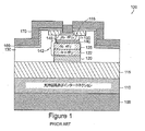
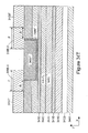
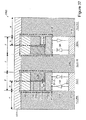
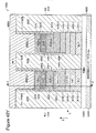
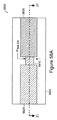
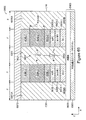
図1に示す従来技術の3D EPROMアレイ100は、米国特許第4,442,507号における従来の対応構造物を示す。メモリセルは、軽くドープされたポリシリコンを用いて、ショットキーダイオードの上側に形成されたアンチヒューズと直列である垂直配向ショットキーダイオードを含む。支持回路及びインターコネクション110は、支持半導体基板105、例えばシリコンの内部及びその上部に形成される。絶縁体115(図1には図示せず)を通じるインターコネクションを用いて支持回路を導電体120及び導電体170のようなアレイラインに連結する。メモリセルは、絶縁体115の表面上に製造され、ショットキーダイオード142及びアンチヒューズ155を含み、組み合わせた導電体120及びN+ポリシリコン導電体122と、金属導電体170及び導電性バリア層160によって相互接続される。絶縁体115の表面が平面のように示されているが、実際には米国特許第4,442,507号に詳述されているように、非平面であり、これは、その発明時点でVLSI平坦化技術を用いることができなかったためである。
The prior art
N+ポリシリコンパターン層半導体122が1つのショットキーダイオード142コンタクト及びアレイインターコネクトラインとして使われる。N+ポリシリコン半導体122は、例えばシリコン又はゲルマニウムであってもよく、通常、抵抗0.04Ohms/squareである1020ドーパントatoms/cm3にドープされる。半導体122がアレイラインとして用いられる場合、N+ポリシリコン半導体122をN+半導体層と絶縁体115の表面の間でモリブデンシリサイド導電体120上に堆積することで、低抵抗のアレイラインが形成できる。半導体122と接触する、第2のN多結晶シリコン又はゲルマニウム半導体パターン層(半導体)125は、通常、抵抗が15Ohms/squareである1014〜1017ドーパントatoms/cm3にドープされ、セル選択デバイスとして用いられるショットキーダイオード142の陰極端子を形成する。ドーパントは、例えばヒ素、リン及びアンチモンであり得る。ポリシリコン導電体122及び125は、通常、厚さ400nmで幅2μmである。
N + polysilicon patterned
ショットキーダイオードデバイス142の陽極は、N多結晶シリコン導電体125上に堆積された25nm厚の白金のような貴金属を用いるパターン導電体140によって形成され、600℃まで加熱されて、下部の多結晶物質と共に化合物(例えば、白金シリサイド)を形成する。貴金属140のシリサイド及び下部のNポリシリコン半導体125は、ショットキーダイオード142のジャンクション145を形成する。ショットキーダイオード142の測定結果、約0.4ボルトのターンオン電圧及び約10ボルトの逆方向耐圧が測定された。
The anode of the Schottky
メモリセルの不揮発性の状態は、抵抗状態としてアンチヒューズ155に記憶される。製造プロセス完了後に、アンチヒューズ155の抵抗状態は、1回(OTP)変更可能(プログラマブルする)である。好ましくは、アンチヒューズ155を形成するために用いられた物質150は、通常、1017atoms/cm3未満にドープされる、シリコン又はゲルマニウムのような単元素N半導体であり、ここで、米国特許第4,442,507号に詳述されているように、ヒ素及びリンが適したN型ドーパントとなる。アンチヒューズ155を形成するためのパターニング後に、TiW100nm厚の導電性バリア層160が、アンチヒューズ155及び絶縁体130に接触して堆積される。その後、80nmのアルミニウム層が堆積及びパターニングされて導電体170を形成する。導電体170及び導電性バリア層160の全てがパターニングされる。導電性バリア層160を用いて、アルミニウムのNポリシリコン物質150内への移動を防止する。
The nonvolatile state of the memory cell is stored in the
アンチヒューズの抵抗は、形成されたままの状態で通常、107オームである。まず、全てのセル内の全てのアンチヒューズは、製造された状態で約107オームの抵抗値を有する。約10ボルトのアンチヒューズ閾値電圧に達するように、セルが選択されてプログラムされれば、アンチヒューズ抵抗は102オームに変わり、プログラミング電流は約50μAに制限され、プログラミング時間は、マイクロ秒範囲となる。アンチヒューズが1回のみプログラムされてもよく、半導体基板105内及び半導体基板105上の下部支持回路110上側のアレイ領域を用いて不揮発性の新しい低抵抗状態が3D EPROMメモリのメモリセル内に記憶される。
Resistance of the antifuse is normally in a state of as-formed, it is 107 ohms. First, all antifuses in all cells have a resistance value of about 10 7 ohms as manufactured. To reach the antifuse threshold voltage of about 10 volts, if the cell is selected and programmed anti-fuse resistance will change to 10 2 ohms, the programming current is limited to approximately 50 .mu.A, the programming time, and microseconds range Become. The anti-fuse may be programmed only once, and a new nonvolatile low resistance state is stored in the memory cell of the 3D EPROM memory using the array region above the
全てのセル成分及びインターコネクションが半導体基板及び前記支持回路から分離された3D EPROMメモリアレイの概念が米国特許第4,442,507号に提示されているが、そのような接近方式はOTPメモリに制限される。 The concept of a 3D EPROM memory array in which all cell components and interconnections are separated from the semiconductor substrate and the supporting circuit is presented in U.S. Pat. No. 4,442,507. Limited.
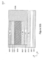
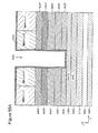
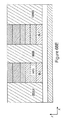
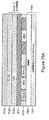
従来技術に関する図2は、参照のためにその全体を本願に引用する、Ryan、J.G.らが「The evolution of interconnection technology at IBM」、Journal of Research and Development,Vol,39,No.4,July 1995,pp.371−381に記載した従来技術であって、平面ローカルインターコネクト金属層及び4つ(金属1〜金属4)の導電体の付加的なよりグローバルの平面積層レベルを有するデバイスと、積層コンタクト及び充填されたビアホール(コンタクトスタッド)を含む製造されたCMOS構造200及び200’が示されている。金属5は、非平面であり、外部連結を提供するために用いられる。ローカルインターコネクト及び配線層金属1、金属2、金属3、金属4及び金属5は、例えばAl(Cu)、W、Mo、Ti、Cuを用いてもよい。厳格な金属ピッチは、金属及び酸化物に対する平坦化を要求し、図2に示すように、タングステン(W)を用いて通常形成されるほぼ垂直のゼロオーバーラップビアスタッドを要求する。化学機械研磨(CMP)平坦化技術の広範な利用によって構造物200及び200’の形成が可能となった。CMP技術もまた、参照のためにその全体を本願に引用する、1990年7月31日出願の米国特許第4,944,836号に説明されている。CMP技術も従来レベルの欠陥を除去し得る能力より選択された。
FIG. 2 relating to the prior art is incorporated by reference in its entirety for reference. G. Et al., “The evolution of interconnection technology at IBM”, Journal of Research and Development, Vol. 4, July 1995, pp. 371-381, a device having an additional more global planar stacking level of planar local interconnect metal layers and four (
参照のためにその全体を本願に引用し、共同発明者Bertinに許与された米国特許第5,670,803号には、同時に規定される側壁寸法を有する3D SRAMアレイ構造物が開示されている。このような構造物は、複数の整列段階を避けるために(最小化するために)、複数のドープされたシリコン及び絶縁領域を通過するトレンチによって同時に規定される垂直側壁を含む。これらのトレンチは、複数の半導体及び酸化物層を通過し、3D SRAMアレイ構造物と下部半導体基板の間の支持絶縁体(SiO2)層の上部表面上で終了する。米国特許第5,670,803号にも垂直配線3D SRAMセルを形成するために、トレンチ領域内のイントレンチ垂直ローカルセルインターコネクト配線が開示されている。また、米国特許第5,670,803号には、さらに、トレンチ領域を通じてトレンチセル内で局部的に配線された3D SRAMストレージセルの上部表面まで延長される貫通トレンチ垂直インターコネクト配線が開示されている。
[関連出願の相互参照]
U.S. Pat. No. 5,670,803, which is incorporated herein by reference in its entirety and granted to co-inventor Bertin, discloses a 3D SRAM array structure having sidewall dimensions defined simultaneously. Yes. Such a structure includes vertical sidewalls that are simultaneously defined by a plurality of doped silicon and trenches passing through an insulating region to avoid (minimize) multiple alignment steps. These trenches pass through a plurality of semiconductor and oxide layers and terminate on the upper surface of the support insulator (SiO 2 ) layer between the 3D SRAM array structure and the lower semiconductor substrate. U.S. Pat. No. 5,670,803 also discloses in-trench vertical local cell interconnect wiring in the trench region to form vertical wiring 3D SRAM cells. U.S. Pat. No. 5,670,803 further discloses a through-trench vertical interconnect wiring that extends to the top surface of a 3D SRAM storage cell that is locally wired in the trench cell through the trench region. .
[Cross-reference of related applications]
本願は、米国特許法第119条(e)項の下に以下の出願に対して優先権の権利請求をし、これら出願の全内容は参照により本明細書に引用したものとする。
米国仮特許出願第60/855,109号、2006年10月27日出願、名称「Nonvolatile Nanotube Blocks」、
米国仮特許出願第60/840,586号、2006年8月28日出願、名称「Nonvolatile Nanotube Diode」、
米国仮特許出願第60/836,437号、2006年8月8日出願、名称「Nonvolatile Nanotube Diode」、
米国仮特許出願第60/836,343号、2006年8月8日出願、名称「Scalable Nonvolatile Nanotube Switches as Electronic Fuse Replacement Elements」、
米国仮特許出願第60/918,388号、2007年3月16日出願、名称「Memory Elements and Cross Point Switches and Arrays of Same Using Nonvolatile Nanotube Blocks」。
This application claims priority to the following applications under 35 USC 119 (e), the entire contents of which are hereby incorporated by reference:
US Provisional Patent Application No. 60 / 855,109, filed Oct. 27, 2006, entitled “Nonvolatile Nanotube Blocks”,
U.S. Provisional Patent Application No. 60 / 840,586, filed August 28, 2006, name "Nonvolatile Nanotube Diode",
U.S. Provisional Patent Application No. 60 / 836,437, filed August 8, 2006, named "Nonvolatile Nanotube Diode",
US Provisional Patent Application No. 60 / 836,343, filed Aug. 8, 2006, entitled “Scalable Nonvolatile Nanotubes as Electronic Fuse Replacement Elements”,
US Provisional Patent Application No. 60 / 918,388, filed Mar. 16, 2007, entitled “Memory Elements and Cross Point Switches and Arrays of Something Nanotubes”.
本願は、米国特許法第120条の下に以下の出願に対して優先権の権利請求をし、一部継続出願し、これら出願の全内容は参照により本明細書に引用したものとする。
米国特許出願第11/280,786号、2005年11月27日出願、名称「Two−Terminal Nanotube Devices And Systems And Methods Of Making Same」、
米国特許出願第11/274,967号、2005年11月15日出願、名称「Memory Arrays Using Nanotube Articles With Reprogrammable Resistance」、
米国特許出願第11/280,599号、2005年11月15日出願、名称「Non−Volatile Shadow Latch Using A Nanotube Switch」。
This application claims priority to the following applications under 35
US Patent Application No. 11 / 280,786, filed November 27, 2005, entitled “Two-Terminal Nanotube Devices And Methods Of Making Same”,
U.S. Patent Application No. 11 / 274,967, filed on November 15, 2005, entitled "Memory Arrays Using Nanotubes With Reprogrammable Resistance",
US Patent Application No. 11 / 280,599, filed on November 15, 2005, entitled “Non-Volatile Shadow Latching A Nanotube Switch”.
本願は、本願と同時に出願された以下の出願と連関し、これら出願の全内容は参照により本明細書に引用したものとする。
米国特許出願第(番号未定)号、名称「Nonvolatile Resistive Memories Having Scalable Two−Terminal Nanotube Switches」、
米国特許出願第(番号未定)号、名称「Latch Circuits and Operation Circuits Having Scalable Nonvolatile Nanotube Switches as Electronic Fuse Replacement Elements」、
米国特許出願第(番号未定)号、名称「Memory Elements and Cross Point Switches and Arrays of Same Using Nonvolatile Nanotube Blocks」、
米国特許出願第(番号未定)号、名称「Nonvolatile Nanotube Diodes and Nonvolatile Nanotube Blocks and Systems Using Same and Methods of Making Same」、
米国特許出願第(番号未定)号、名称「Nonvolatile Nanotube Diodes and Nonvolatile Nanotube Blocks and Systems Using Same and Methods of Making Same」、
米国特許出願第(番号未定)号、名称「Nonvolatile Nanotube Diodes and Nonvolatile Nanotube Blocks and Systems Using Same and Methods of Making Same」、
米国特許出願第(番号未定)号、名称「Nonvolatile Nanotube Diodes and Nonvolatile Nanotube Blocks and Systems Using Same and Methods of Making Same」、
米国特許出願第(番号未定)号、名称「Nonvolatile Nanotube Diodes and Nonvolatile Nanotube Blocks and Systems Using Same and Methods of Making Same」。
This application is related to the following applications filed at the same time as the present application, and the entire contents of these applications are incorporated herein by reference.
US Patent Application No. (No TBD), “Nonvolatile Resistive Memories Having Stable Two-Terminal Nanotube Switches”,
US Patent Application No. (No TBD), “Latch Circuits and Operation Circuits Having Stable Nonvolatiles Nanotube Switches as Electronic Fuse Replacement Elements”
US Patent Application No. (undecided), name “Memory Elements and Cross Point Switches and Arrays of Some Using Nonvolatile Blocks,”
U.S. Patent Application (No TBD), Name “Nonvolatile Nanotube Diodes and Nonvolatile Nanotube Blocks and Systems Using Same and Methods of Making Same”
U.S. Patent Application (No TBD), Name “Nonvolatile Nanotube Diodes and Nonvolatile Nanotube Blocks and Systems Using Same and Methods of Making Same”
U.S. Patent Application (No TBD), Name “Nonvolatile Nanotube Diodes and Nonvolatile Nanotube Blocks and Systems Using Same and Methods of Making Same”
U.S. Patent Application (No TBD), Name “Nonvolatile Nanotube Diodes and Nonvolatile Nanotube Blocks and Systems Using Same and Methods of Making Same”
United States Patent Application No. (No TBD), “Nonvolatile Nanotube Diodes and Nonvolatile Nanotube Blocks and Systems Using Same and Methods of Making Same”.
本発明は、不揮発性ナノチューブダイオード及び不揮発性ナノチューブブロック、並びにそれらを用いるシステム及びその製造方法を提供する。 The present invention provides a nonvolatile nanotube diode and a nonvolatile nanotube block, a system using them, and a method for manufacturing the same.
1つの態様において、不揮発性ナノチューブダイオードデバイスは、第1及び第2端子と、陰極及び両極を含み、前記第1導電端子に印加される電気刺激に応答して、前記陰極と陽極の間に導電経路を形成し得る半導体素子と、前記半導性素子と電気的に導通するナノチューブファブリック部材(nanotube fabric article)を含むナノチューブスイッチング素子とを含み、前記ナノチューブファブリック部材は、前記半導体素子と前記第2端子の間に配置されて、その間で導電経路を形成することができ、前記第1及び第2端子に対する電気刺激は、複数のロジッグ状態を招く。 In one aspect, a non-volatile nanotube diode device includes first and second terminals, a cathode and bipolar electrodes, and is electrically conductive between the cathode and anode in response to electrical stimulation applied to the first conductive terminal. A semiconductor element capable of forming a path, and a nanotube switching element including a nanotube fabric member that is in electrical communication with the semiconductive element, wherein the nanotube fabric member includes the semiconductor element and the second element. Between the terminals, a conductive path can be formed therebetween, and electrical stimulation to the first and second terminals results in a plurality of logic states.
1つ以上の実施例は、以下の特徴のうち1つ以上を含む。複数のロジック状態のうち第1ロジッグ状態において、第1及び第2端子の間の導電経路は実質的に無効になり、前記複数のロジッグ状態のうち第2ロジッグ状態において、前記第1及び第2端子の間の導電経路は有効になる。第1ロジッグ状態において、ナノチューブ部材は相対的に高い抵抗を有し、第2ロジッグ状態においてナノチューブ部材は相対的に低い抵抗を有する。ナノチューブファブリック部材は、非整列ナノチューブの不織網を含む。第2ロジック状態において、非整列ナノチューブの不織網は、半導体素子と第2端子の間の1つ以上の導電経路を含む。ナノチューブファブリック部材は、多層ファブリックである。第1及び第2端子の間の閾値電圧以上で半導体素子は、陽極から陰極へ電流を流動させることができ、第1及び第2端子の間の閾値未満で半導体素子は、陽極から陰極へ電流を流動させることができない。第1ロジッグ状態において、陽極と第2端子の間の導電経路は、無効になり。第2ロジッグ状態において、陽極と第2端子の間の導電経路は、有効になる。導電性コンタクトがナノチューブファブリック部材と半導体素子の間に配置され、その間で電気導通経路を提供する。第1端子は陽極と電気的に導通され、陰極はナノチューブスイッチング素子の導電性コンタクトと電気的に導通される。第2ロジッグ状態においてデバイスは、第1端子から第2端子へ実質的に流れる電流を伝達することができる。第1端子は、陰極と電気的に導通され、陽極はナノチューブスイッチング素子の導電性コンタクトと電気的に導通される。第2ロジッグ状態にあるとき、デバイスは、第2端子から第1端子へ実質的に流れる電流を伝達することができる。陽極は導電性物質を含み、陰極はn型半導体物質を含む。陽極はp型半導体物質を含み、陰極はn型半導体物質を含む。 One or more embodiments include one or more of the following features. In the first logic state of the plurality of logic states, the conductive path between the first and second terminals is substantially disabled, and in the second logic state of the plurality of logic states, the first and second The conductive path between the terminals becomes effective. In the first logig state, the nanotube member has a relatively high resistance, and in the second logig state, the nanotube member has a relatively low resistance. The nanotube fabric member includes a nonwoven network of non-aligned nanotubes. In the second logic state, the non-aligned nanotube nonwoven network includes one or more conductive paths between the semiconductor element and the second terminal. The nanotube fabric member is a multi-layer fabric. Above the threshold voltage between the first and second terminals, the semiconductor element can flow a current from the anode to the cathode, and below the threshold voltage between the first and second terminals, the semiconductor element has a current from the anode to the cathode. Can not flow. In the first logic state, the conductive path between the anode and the second terminal is disabled. In the second logic state, the conductive path between the anode and the second terminal is enabled. Conductive contacts are disposed between the nanotube fabric member and the semiconductor element and provide an electrical conduction path therebetween. The first terminal is electrically connected to the anode and the cathode is electrically connected to the conductive contact of the nanotube switching element. In the second logic state, the device can transfer a current that substantially flows from the first terminal to the second terminal. The first terminal is electrically connected to the cathode, and the anode is electrically connected to the conductive contact of the nanotube switching element. When in the second logic state, the device can transfer a current that substantially flows from the second terminal to the first terminal. The anode includes a conductive material, and the cathode includes an n-type semiconductor material. The anode includes a p-type semiconductor material and the cathode includes an n-type semiconductor material.
別の態様において、2端子不揮発性状態デバイスは、第1及び第2端子と、ソース、ドレイン、前記ソース及びドレインの何れかと電気的に導通するゲート、及び前記ソースとドレインの間に配置されたチャネルを備える半導体電界効果素子であって、前記ゲートが前記ソースと前記ドレインの間のチャネル内に導電経路を制御可能に形成し得る半導体電界効果素子と、ナノチューブファブリック部材及び導電性コンタクトを備えるナノチューブスイッチング素子であって、前記ナノチューブファブリック部材は、前記導電性コンタクトと前記第2端子の間に配置され、その間で導電経路を形成し得るナノチューブスイッチング素子とを含み、前記第1端子は、前記ソース及びドレインの一方と電気的に導通し、前記ソースとドレインの他方は、前記導電性コンタクトと電気的に導通し、前記第1及び第2導電端子に対する第1の電気刺激セットが前記第1ロジッグ状態を招き、前記第1及び第2導電端子に対する第2の電気刺激セットは第2ロジッグ状態を招く。 In another aspect, a two-terminal nonvolatile state device is disposed between the first and second terminals, a source, a drain, a gate in electrical communication with any of the source and drain, and the source and drain. A semiconductor field effect device comprising a channel, the nanotube comprising a nanotube fabric member and a conductive contact, wherein the gate can controllably form a conductive path in the channel between the source and the drain A switching element, the nanotube fabric member including a nanotube switching element disposed between the conductive contact and the second terminal and capable of forming a conductive path therebetween, wherein the first terminal is the source And the other of the source and drain. Electrically conducting with the conductive contact, a first electrical stimulation set for the first and second conductive terminals causes the first logic state, and a second electrical stimulation for the first and second conductive terminals The set invites a second logic state.
1つ以上の実施例は、以下の特徴のうち1つ以上を含む。第1ロジッグ状態は、第1及び第2端子の間の相対的な非導電経路に相当し、第2ロジッグ状態は、前記第1及び第2端子の間の導電経路に相当する。第1の電気刺激セットは、ナノチューブファブリック部材内の相対的に高い抵抗状態を招き、第2の電気刺激セットは、ナノチューブファブリック部材内の相対的に低い抵抗状態を招く。ナノチューブファブリック部材は、非整列ナノチューブの不織網を含む。ナノチューブファブリック部材は、多層ファブリックを含む。第2の電気刺激セットに応答して、非整列ナノチューブの不織網は、導電性コンタクトと半導体電界効果素子の間の少なくとも1つの導電経路を提供する。第2の電気刺激セットに応答して、ソースとドレインの間の導電経路が導電性チャネル内に形成される。半導体電界効果素子はPFETを含む。半導体電界効果素子はNFETを含む。半導体電界効果素子のソースは第1端子と電気的に導通し、ドレインはナノチューブスイッチング素子の導電性コンタクトと電気的に導通する。半導体電界効果素子のドレインは第1端子と電気的に導通し、ソースはナノチューブスイッチング素子の導電性コンタクトと電気的に導通する。 One or more embodiments include one or more of the following features. The first logic state corresponds to a relative non-conductive path between the first and second terminals, and the second logic state corresponds to a conductive path between the first and second terminals. The first electrical stimulation set results in a relatively high resistance state in the nanotube fabric member, and the second electrical stimulation set results in a relatively low resistance state in the nanotube fabric member. The nanotube fabric member includes a nonwoven network of non-aligned nanotubes. The nanotube fabric member includes a multi-layer fabric. In response to the second electrical stimulation set, the non-aligned nanotube nonwoven network provides at least one conductive path between the conductive contact and the semiconductor field effect element. In response to the second electrical stimulation set, a conductive path between the source and drain is formed in the conductive channel. The semiconductor field effect element includes a PFET. The semiconductor field effect element includes an NFET. The source of the semiconductor field effect element is electrically connected to the first terminal, and the drain is electrically connected to the conductive contact of the nanotube switching element. The drain of the semiconductor field effect element is electrically connected to the first terminal, and the source is electrically connected to the conductive contact of the nanotube switching element.
別の態様において、電圧選択回路は、入力電圧ソースと、出力電圧端子及び基準電圧端子と、抵抗素子と、不揮発性ナノチューブダイオードデバイスとを含み、前記ナノチューブダイオードデバイスは、第1及び第2端子と、前記第1端子と電気的に導通する半導体素子と、前記半導体素子と前記第2端子の間に配置され、その間で電気刺激を伝達し得るナノチューブスイッチング素子とを含み、前記不揮発性ナノチューブダイオードデバイスは、第1及び第2端子の間で電気刺激を伝達することができ、前記抵抗素子は、前記入力電圧ソースと前記出力電圧端子の間に配置され、前記不揮発性ナノチューブダイオードデバイスは、前記出力の電圧端子と基準電圧端子の間に配置されて、その間で電気的に導通され、前記電圧選択回路は、入力電圧ソース及び基準電圧端子における電気刺激に応答して、不揮発性ナノチューブダイオードが第1及び第2端子の間における電気刺激の伝達を実質的に防止するとき、第1出力電圧レベルを提供することができ、前記電圧選択回路は、入力電圧ソース及び基準電圧端子における電気刺激に応答して、不揮発性ナノチューブダイオードが第1及び第2端子の間における電気刺激を伝達するとき、第2出力電圧レベルを提供することができる。 In another aspect, the voltage selection circuit includes an input voltage source, an output voltage terminal and a reference voltage terminal, a resistance element, and a nonvolatile nanotube diode device, wherein the nanotube diode device includes first and second terminals. A non-volatile nanotube diode device, comprising: a semiconductor element electrically conducting with the first terminal; and a nanotube switching element disposed between the semiconductor element and the second terminal and capable of transmitting electrical stimulation therebetween. Can transmit electrical stimulation between first and second terminals, the resistive element is disposed between the input voltage source and the output voltage terminal, and the non-volatile nanotube diode device is configured to output the output Between the voltage terminal and the reference voltage terminal and electrically connected between the voltage terminal and the reference voltage terminal. Providing a first output voltage level when the non-volatile nanotube diode substantially prevents transmission of electrical stimulation between the first and second terminals in response to electrical stimulation at the voltage source and reference voltage terminals. The voltage selection circuit may be configured to output a second output voltage level when the non-volatile nanotube diode transmits electrical stimulation between the first and second terminals in response to electrical stimulation at the input voltage source and reference voltage terminals. Can be provided.
1つ以上の実施例が以下の特徴のうち1つ以上を含む。半導体素子が陽極及び陰極を含み、前記陽極は第1端子と電気的に導通し、前記陰極はナノチューブスイッチング素子と導通する。半導体素子は、第1端子と導通するソース領域、ナノチューブスイッチング素子と電気的に導通するドレイン領域、前記ソース領域とドレイン領域の何れかと電気的に導通するゲート領域、及び前記ゲート領域に対する電気刺激に応答して、前記ソースと前記ドレインの間の導電経路を制御可能に形成、又は形成しないことができるチャネル領域を有する電界効果素子を含む。第1出力電圧レベルは、入力電圧ソースと実質的に等しい。第2出力電圧レベルは、基準電圧端子と実質的に等しい。ナノチューブスイッチング素子は、高抵抗状態及び低抵抗状態が可能なナノチューブファブリック部材を含む。ナノチューブファブリック部材の高抵抗状態は、抵抗素子の抵抗よりも実質的に高く、前記ナノチューブファブリック部材の低抵抗状態は、抵抗素子の抵抗よりも実質的に低い。第1出力電圧レベルは、部分的に、抵抗素子の相対的な抵抗及びナノチューブファブリック部材の高抵抗状態によって決定され、第2出力電圧レベルは、部分的に、抵抗素子の相対的な抵抗及びナノチューブファブリック部材の低抵抗状態によって決定される。 One or more embodiments include one or more of the following features. The semiconductor element includes an anode and a cathode, the anode is in electrical communication with the first terminal, and the cathode is in communication with the nanotube switching element. The semiconductor element includes a source region electrically connected to the first terminal, a drain region electrically connected to the nanotube switching element, a gate region electrically connected to any one of the source region and the drain region, and electrical stimulation to the gate region. In response, it includes a field effect element having a channel region that can controllably form or not form a conductive path between the source and the drain. The first output voltage level is substantially equal to the input voltage source. The second output voltage level is substantially equal to the reference voltage terminal. The nanotube switching element includes a nanotube fabric member capable of a high resistance state and a low resistance state. The high resistance state of the nanotube fabric member is substantially higher than the resistance of the resistance element, and the low resistance state of the nanotube fabric member is substantially lower than the resistance of the resistance element. The first output voltage level is determined in part by the relative resistance of the resistive element and the high resistance state of the nanotube fabric member, and the second output voltage level is partially determined by the relative resistance of the resistive element and the nanotube. It is determined by the low resistance state of the fabric member.
別の態様において、不揮発性ナノチューブダイオードは、基板と、前記基板にかけて配置された半導体素子であって、陽極と陰極を有し、前記陽極と前記陰極の間の導電経路を形成することができる半導体素子と、前記半導体素子にかけて配置されたナノチューブスイッチング素子であって、複数の抵抗状態を有することができるナノチューブファブリック素子及び導電性コンタクトを含むナノチューブスイッチング素子と、前記導電性コンタクトに対して相対的に離隔して配置された導電端子とを含み、前記ナノチューブファブリック素子は、前記導電性コンタクトとの間に配置されて、前記導電性コンタクトと電気的に導通し、前記導電性コンタクトは陰極と電気的に導通し、前記陽極及び導電端子に印加された電気刺激に応答して、前記不揮発性ナノチューブダイオードが前記陽極と導電性コンタクトの間の導電経路を形成することができる。 In another aspect, a non-volatile nanotube diode is a semiconductor element disposed over a substrate and the substrate, the semiconductor device having an anode and a cathode and capable of forming a conductive path between the anode and the cathode A nanotube switching element disposed over the semiconductor element, the nanotube switching element including a nanotube fabric element and a conductive contact that can have a plurality of resistance states, and relative to the conductive contact The nanotube fabric element is disposed between the conductive contacts and electrically connected to the conductive contacts, and the conductive contacts are electrically connected to the cathode. In response to an electrical stimulus applied to the anode and the conductive terminal. It can be nonvolatile nanotube diode to form a conductive path between the anode and the conductive contact.
1つ以上の実施例が以下の特徴のうち1つ以上を含む。陽極は導電体物質を含み、陰極は半導体物質を含む。陽極物質は、Al、Ag、Au、Ca、Co、Cr、Cu、Fe、Ir、Mg、Mo、Na、Ni、Os、Pb、Pd、Pt、Rb、Ru、Ti、W、Zn、CoSi2、MoSi2、Pd2Si、PtSi、RbSi2、TiSi2、WSi2及びZrSi2のうち少なくとも1つを含む。半導体素子は、ショットキーバリアダイオードを含む。第2導電端子が基板と陽極の間に配置され、陽極と電気的に導通し、前記第2導電端子と前記導電端子における電気刺激に応答して、前記不揮発性ナノチューブダイオードが前記第2導電端子と前記導電端子の間の導電経路を形成することができる。前記陽極は第1型の半導体物質を含み、前記陰極領域は第2型の半導体物質を含む。第1型の半導体物質は正にドープされ、第2型の半導体物質は負にドープされ、半導体素子がPNジャンクションを形成する。ナノチューブファブリック素子は、実質的に垂直配置される。ナノチューブファブリック素子は、実質的に水平配置される。ナノチューブファブリック素子は、不織多層ファブリックを含む。ナノチューブファブリック素子の厚さは、約20nm〜約200nmである。導電性コンタクトは、ナノチューブファブリック素子の下部表面と実質的に同一平面内に配置され、導電端子は、ナノチューブファブリック素子の上部表面と実質的に同一平面内に配置される。半導体素子は、電界効果トランジスタである。 One or more embodiments include one or more of the following features. The anode includes a conductive material and the cathode includes a semiconductor material. The anode material is Al, Ag, Au, Ca, Co, Cr, Cu, Fe, Ir, Mg, Mo, Na, Ni, Os, Pb, Pd, Pt, Rb, Ru, Ti, W, Zn, CoSi 2. comprises MoSi 2, Pd 2 Si, PtSi , at least one of RbSi 2, TiSi 2, WSi 2 and ZrSi 2. The semiconductor element includes a Schottky barrier diode. A second conductive terminal is disposed between the substrate and the anode, is electrically connected to the anode, and the nonvolatile nanotube diode is responsive to electrical stimulation at the second conductive terminal and the conductive terminal. And a conductive path between the conductive terminal and the conductive terminal. The anode includes a first type semiconductor material, and the cathode region includes a second type semiconductor material. The first type semiconductor material is positively doped, the second type semiconductor material is negatively doped, and the semiconductor element forms a PN junction. The nanotube fabric elements are arranged substantially vertically. The nanotube fabric elements are arranged substantially horizontally. The nanotube fabric element includes a non-woven multilayer fabric. The thickness of the nanotube fabric element is about 20 nm to about 200 nm. The conductive contact is disposed in substantially the same plane as the lower surface of the nanotube fabric element, and the conductive terminal is disposed in substantially the same plane as the upper surface of the nanotube fabric element. The semiconductor element is a field effect transistor.
別の態様において、不揮発性ナノチューブダイオードは、基板と、前記基板にかけて配置された導電端子と、前記導電端子にかけて配置された半導体素子であって、陽極と陰極を有し、前記陽極と前記陰極の間の導電経路を形成し得る半導体素子と、前記半導体素子にかけて配置されたナノチューブスイッチング素子であって、複数の抵抗状態を有することができるナノチューブファブリック素子及び導電性コンタクトを含むナノチューブスイッチング素子とを含み、前記ナノチューブファブリック素子は、前記陽極と前記導電性コンタクトの間に配置され、その間で電気的に導通し、前記陰極は導電端子と電気的に導通し、前記陽極及び導電端子に印加された電気刺激に応答して、前記不揮発性ナノチューブダイオードが導電端子と導電性コンタクトの間の導電経路を形成することができる。 In another aspect, the nonvolatile nanotube diode is a substrate, a conductive terminal disposed over the substrate, and a semiconductor element disposed over the conductive terminal, the anode and the cathode, the anode and the cathode A semiconductor device capable of forming a conductive path therebetween, and a nanotube switching element disposed over the semiconductor element, the nanotube switching element including a plurality of resistance states and a nanotube switching element including a conductive contact The nanotube fabric element is disposed between the anode and the conductive contact, and is electrically connected between the anode and the cathode. The cathode is electrically connected to a conductive terminal, and an electric current applied to the anode and the conductive terminal. In response to a stimulus, the non-volatile nanotube diode is electrically connected to a conductive terminal. It is possible to form a conductive path between the Ntakuto.
1つ以上の実施例が以下の特徴のうち1つ以上を含む。陽極は導電体物質を含み、陰極は半導体物質を含む。陽極物質は、Al、Ag、Au、Ca、Co、Cr、Cu、Fe、Ir、Mg、Mo、Na、Ni、Os、Pb、Pd、Pt、Rb、Ru、Ti、W、Zn、CoSi2、MoSi2、Pd2Si、PtSi、RbSi2、TiSi2、WSi2及びZrSi2のうち少なくとも1つを含む。半導体素子は、ショットキーバリアダイオードを含む。第2導電端子が不織ナノチューブファブリックのパターニングされた領域と陽極の間に配置され、その間の導電経路を提供する。前記陽極は第1型の半導体物質を含み、前記陰極領域は第2型の半導体物質を含む。第1型の半導体物質は正にドープされ、第2型の半導体物質は負にドープされ、半導体素子がPNジャンクションを形成する。ナノチューブファブリック素子は、実質的に垂直配置される。ナノチューブファブリック素子は、実質的に水平配置される。ナノチューブファブリック素子は、厚さが約0.5〜約20ナノメートルの不織ナノチューブ層を含む。ナノチューブファブリック素子は、不織多層ファブリックを含む。導電性コンタクトは、ナノチューブファブリック素子の下部表面と実質的に同一平面内に配置され、導電端子は、ナノチューブファブリック素子の上部表面と実質的に同一平面内に配置される。半導体素子は、電界効果トランジスタを含む。 One or more embodiments include one or more of the following features. The anode includes a conductive material and the cathode includes a semiconductor material. The anode material is Al, Ag, Au, Ca, Co, Cr, Cu, Fe, Ir, Mg, Mo, Na, Ni, Os, Pb, Pd, Pt, Rb, Ru, Ti, W, Zn, CoSi 2. comprises MoSi 2, Pd 2 Si, PtSi , at least one of RbSi 2, TiSi 2, WSi 2 and ZrSi 2. The semiconductor element includes a Schottky barrier diode. A second conductive terminal is disposed between the patterned region of the nonwoven nanotube fabric and the anode and provides a conductive path therebetween. The anode includes a first type semiconductor material, and the cathode region includes a second type semiconductor material. The first type semiconductor material is positively doped, the second type semiconductor material is negatively doped, and the semiconductor element forms a PN junction. The nanotube fabric elements are arranged substantially vertically. The nanotube fabric elements are arranged substantially horizontally. The nanotube fabric element includes a non-woven nanotube layer having a thickness of about 0.5 to about 20 nanometers. The nanotube fabric element includes a non-woven multilayer fabric. The conductive contact is disposed in substantially the same plane as the lower surface of the nanotube fabric element, and the conductive terminal is disposed in substantially the same plane as the upper surface of the nanotube fabric element. The semiconductor element includes a field effect transistor.
別の態様において、メモリアレイが複数のワードラインと、複数のビットラインと、複数のメモリセルとを含み、各々の前記メモリセルがワードライン及びビットラインに対する電気刺激に応答し、各々の前記メモリセルは、第1及び第2端子を含む2端子不揮発性ナノチューブスイッチングデバイス、半導体ダイオード素子、及びナノチューブファブリック部材を含み、半導体ダイオード及びナノチューブ部材が前記第1及び第2端子の間に配置されて、その間で電気的に導通し、前記ナノチューブファブリック部材は、複数の抵抗状態を有することができ、前記第1端子は1つのワードラインにカップリングされ、第2端子は1つのビットラインにカップリングされ、前記第1及び第2端子に印加された電気刺激は、ナノチューブファブリック部材の抵抗状態を変化させることができ、メモリ操作回路は、複数のビットラインのうち各ビットラインと、複数のワードラインのうち各ワードラインに動作可能にカップリングされ、前記操作回路は、対応する第1及び第2端子の各々に選択された電気刺激を印加するために、セルにカップリングされたビットライン及びワードラインのうち少なくとも1つを活性化させることで、セルのうち各々のセルを選択することができ、前記操作回路は、さらに、選択されたメモリセルのナノチューブファブリック部材の抵抗状態を検出すること、及び、ナノチューブファブリック部材内の選択された抵抗状態を制御可能に誘導するために、抵抗状態に応答して対応する第1及び第2端子の各々に印加される電気刺激を調整することができ、前記各メモリセルのナノチューブファブリック部材の選択された抵抗状態は、前記メモリセルの情報状態に対応する。 In another aspect, a memory array includes a plurality of word lines, a plurality of bit lines, and a plurality of memory cells, each of the memory cells responsive to electrical stimulation to the word lines and bit lines, and each of the memory The cell includes a two-terminal nonvolatile nanotube switching device including first and second terminals, a semiconductor diode element, and a nanotube fabric member, wherein the semiconductor diode and the nanotube member are disposed between the first and second terminals, Electrically conducting therebetween, the nanotube fabric member can have a plurality of resistance states, the first terminal is coupled to one word line and the second terminal is coupled to one bit line. The electrical stimulation applied to the first and second terminals is a nanotube fab. The memory operation circuit is operatively coupled to each bit line of the plurality of bit lines and each word line of the plurality of word lines, and the operation circuit includes: Each of the cells by activating at least one of a bit line and a word line coupled to the cell to apply a selected electrical stimulus to each of the corresponding first and second terminals. The operation circuit further detects the resistance state of the nanotube fabric member of the selected memory cell and controllably induces the selected resistance state in the nanotube fabric member In order to adjust the electrical stimulation applied to each of the corresponding first and second terminals in response to the resistance state, Serial selected resistance state of the nanotube fabric member of each memory cell corresponds to the information state of the memory cell.
1つ以上の実施例が以下の特徴のうち1つ以上を含む。各メモリセルは、対応する第1及び第2端子の各々に印加された電気刺激に応答して、対応情報状態を不揮発的に記憶する。半導体ダイオード素子は、陰極及び陽極を含み、前記陽極は第2端子と電気的に導通し、前記陰極はナノチューブスイッチング素子と電気的に導通する。前記陰極は第1半導体物質を含み、前記陽極は第2半導体物質を含む。半導体ダイオード素子は陰極及び陽極を含み、前記陰極は第1端子と電気的に導通し、前記陽極はナノチューブスイッチング素子と電気的に導通する。前記陰極は第1半導体物質を含み、前記陽極は第2半導体物質を含む。前記陰極は半導体物質を含み、前記陽極は導電性物質を含み、ナノチューブファブリック部材に対する導電性コンタクトを形成する。導電性コンタクトが半導体ダイオード素子とナノチューブファブリック部材の間に位置される。前記ナノチューブファブリック部材は、第1及び第2端子のうち1つと第1導電性コンタクトの間の少なくとも1つの導電経路を提供し得る非整列ナノチューブの網を含む。ナノチューブファブリック部材は、多層ナノチューブファブリックを含む。多層ナノチューブ部材は、第1及び第2導電端子のうち1つと導電性コンタクトの間の間隔を規定する厚さを有する。複数のメモリセルは、積層メモリセルの複数対を含み、前記積層メモリセルの各対内の第1メモリセルは、第1ビットラインの上側でその第1ビットラインと電気的に導通するように配置され、前記ワードラインは、第1メモリセルの上側でその第1メモリセルと電気的に導通するように配置され、前記積層メモリセルの各対内の第2メモリセルは、ワードラインの上側でそのワードラインと電気的に導通するように配置され、第2ビットラインは、第2メモリセルの上側でその第2メモリセルと電気的に導通するように配置される。第1メモリセル内のナノチューブ部材の抵抗状態は、第2メモリセル内のナノチューブ部材の抵抗状態によって実質的に影響されず、前記第2メモリセル内のナノチューブ部材の抵抗状態は、第1メモリセル内のナノチューブ部材の抵抗状態によって実質的に影響されない。第1メモリセル内のナノチューブ部材の抵抗状態は、第2メモリセルを選択する前記操作回路によって実質的に影響されず、前記第2メモリセル内のナノチューブ部材の抵抗状態は、第1メモリセルを選択する前記操作回路による抵抗状態によって実質的に影響されない。第1メモリセル内のナノチューブ部材の抵抗状態は、第2メモリセルのナノチューブファブリック部材の抵抗状態を検出する前記操作回路によって実質的に影響されず、前記第2メモリセル内のナノチューブ部材の抵抗状態は、第1メモリセルのナノチューブファブリック部材の抵抗状態を検出する前記操作回路による抵抗状態によって実質的に影響されない。第1メモリセル内のナノチューブ部材の抵抗状態は、第2メモリセルの対応する第1及び第2端子の各々に印加される電気刺激を調整する前記操作回路によって実質的に影響されず、前記第2メモリセル内のナノチューブ部材の抵抗状態は、第1メモリセルの対応する第1及び第2端子の各々に印加される電気刺激を調整する前記操作回路による抵抗状態によって実質的に影響されない。絶縁領域及び複数の導電性インターコネクトで、絶縁領域がメモリ操作回路の上側にかけて配置され、複数のメモリセルが絶縁領域の上側にかけて配置され、複数の導電性インターコネクトがメモリ操作回路を複数のビットライン及び複数のワードラインに動作可能にカップリングする。電気刺激を調整することは、対応する第1及び第2端子の各々に印加される電圧を漸進的に変化させることを含む。電圧の漸進的な変化は、電圧パルスを印加することを含む。伴われる電圧パルスの振幅は、約200mV漸進的に増大される。電気刺激を印加することは、対応する第1及び第2端子のうち少なくとも1つに供給される電流を変化させることを含む。ナノチューブファブリック部材の選択された抵抗状態を実質的に記憶するために、ナノチューブファブリック部材内の選択された抵抗状態を制御可能に誘導した後、対応するビットライン及びワードラインから電気刺激を実質的に除去する。ナノチューブファブリック部材の抵抗状態を検出することは、対応ビットライン上の電気刺激の時間経過による変化を検出することを更に含む。ナノチューブファブリック部材の抵抗状態を検出することは、対応ビットラインを通じる電流流動を検出することを更に含む。各々の2端子不揮発性ナノチューブスイッチングデバイスで、電流が第2端子から第1端子へ流動することができ、第1端子から第2端子へ流動することは実質的に防止される。対応する第1及び第2端子の各々に電気刺激を印加することで、閾値電圧に達したとき、電流が第2端子から第1端子へ流動することができる。各メモリセルのナノチューブファブリック部材の選択された抵抗状態は、前記メモリセルの第1情報状態に対応する相対的に高い抵抗状態及び前記メモリセルの第2情報状態に対応する相対的に低い抵抗状態のうち1つを含む。各メモリセルの第3情報状態は、電流が第2端子から第1端子へ流動することができる状態に相応し、各メモリセルの第4情報状態は、電流が第1端子から第2端子へ流動することが実質的に防止される状態に相応する。2端子不揮発性ナノチューブスイッチングデバイスは、第1及び第2端子の間の電圧極性に関係なく動作できる。2端子不揮発性ナノチューブスイッチングデバイスは、第1及び第2端子の間の電流流動の方向に関係なく動作できる。複数のメモリセルは、積層メモリセルの複数対を含み、積層メモリセルの各々の対内の第1メモリセルは、第1ビットラインの上側に配置されて、その第1ビットラインと電気的に導通し、前記ワードラインは、前記第1メモリセルの上側に配置されて、前記第1メモリセルと電気的に導通し、絶縁体物質が前記第1メモリセルの上側にかけて配置され、前記積層メモリセルの各々の対内の第2メモリは、第2ワードラインの上側に配置されて、前記第2ワードラインと電気的に導通し、前記第2ワードラインは、前記絶縁体物質の上側に配置され、第2ビットラインは、前記第2メモリセルの上側に配置されて、前記第2メモリセルと電気的に導通する。複数のメモリセルは積層メモリセルの複数対を含み、積層メモリセルの各々の対内の第1メモリセルは、第1ビットラインの上側に配置されて、前記第1ビットラインと電気的に導通し、前記ワードラインは、前記第1メモリセルの上側に配置されて、前記第1メモリセルと電気的に導通し、絶縁体が前記第1メモリセルの上側に配置され、積層メモリセルの各々の対内の第2メモリは、第2ビットラインの上側に配置されて、前記第2ビットラインと電気的に導通し、前記第2ビットラインは、前記絶縁体物質の上側に配置され、前記第2ワードラインは、第2メモリセルの上側に配置されて、前記第2メモリセルと電気的に導通する。 One or more embodiments include one or more of the following features. Each memory cell stores a corresponding information state in a nonvolatile manner in response to an electrical stimulus applied to each of the corresponding first and second terminals. The semiconductor diode element includes a cathode and an anode, the anode is electrically connected to the second terminal, and the cathode is electrically connected to the nanotube switching element. The cathode includes a first semiconductor material, and the anode includes a second semiconductor material. The semiconductor diode element includes a cathode and an anode, the cathode is electrically connected to the first terminal, and the anode is electrically connected to the nanotube switching element. The cathode includes a first semiconductor material, and the anode includes a second semiconductor material. The cathode includes a semiconductor material and the anode includes a conductive material to form a conductive contact to the nanotube fabric member. A conductive contact is located between the semiconductor diode element and the nanotube fabric member. The nanotube fabric member includes a network of non-aligned nanotubes that can provide at least one conductive path between one of the first and second terminals and the first conductive contact. The nanotube fabric member includes a multi-walled nanotube fabric. The multi-walled nanotube member has a thickness that defines a spacing between one of the first and second conductive terminals and the conductive contact. The plurality of memory cells include a plurality of pairs of stacked memory cells, and the first memory cell in each pair of the stacked memory cells is arranged to be electrically connected to the first bit line above the first bit line. The word line is arranged to be electrically connected to the first memory cell above the first memory cell, and the second memory cell in each pair of the stacked memory cells is located above the word line. The second bit line is arranged to be electrically conductive with the word line, and the second bit line is arranged to be electrically conductive with the second memory cell above the second memory cell. The resistance state of the nanotube member in the first memory cell is substantially unaffected by the resistance state of the nanotube member in the second memory cell, and the resistance state of the nanotube member in the second memory cell is the first memory cell. It is substantially unaffected by the resistance state of the inner nanotube member. The resistance state of the nanotube member in the first memory cell is substantially unaffected by the operating circuit that selects the second memory cell, and the resistance state of the nanotube member in the second memory cell is determined by the first memory cell. It is not substantially influenced by the resistance state by the operation circuit to be selected. The resistance state of the nanotube member in the first memory cell is not substantially affected by the operating circuit that detects the resistance state of the nanotube fabric member of the second memory cell, and the resistance state of the nanotube member in the second memory cell. Is substantially unaffected by the resistance state of the operating circuit that detects the resistance state of the nanotube fabric member of the first memory cell. The resistance state of the nanotube member in the first memory cell is substantially unaffected by the operating circuit for adjusting electrical stimulation applied to each of the corresponding first and second terminals of the second memory cell, and The resistance state of the nanotube member in the two memory cells is not substantially affected by the resistance state by the operating circuit that adjusts the electrical stimulation applied to each of the corresponding first and second terminals of the first memory cell. An insulating region and a plurality of conductive interconnects, the insulating region is disposed over the memory operating circuit, the plurality of memory cells are disposed over the insulating region, and the plurality of conductive interconnects connect the memory operating circuit to the plurality of bit lines and Operatively coupled to multiple word lines. Adjusting the electrical stimulation includes gradually changing the voltage applied to each of the corresponding first and second terminals. The gradual change in voltage includes applying a voltage pulse. The amplitude of the accompanying voltage pulse is gradually increased by about 200 mV. Applying the electrical stimulus includes changing a current supplied to at least one of the corresponding first and second terminals. In order to substantially store the selected resistance state of the nanotube fabric member, after the controllable induction of the selected resistance state in the nanotube fabric member, the electrical stimulus is substantially transmitted from the corresponding bit line and word line. Remove. Detecting the resistance state of the nanotube fabric member further includes detecting changes over time of electrical stimulation on the corresponding bit line. Detecting the resistance state of the nanotube fabric member further includes detecting current flow through the corresponding bit line. In each two-terminal non-volatile nanotube switching device, current can flow from the second terminal to the first terminal, and flow from the first terminal to the second terminal is substantially prevented. By applying electrical stimulation to each of the corresponding first and second terminals, current can flow from the second terminal to the first terminal when the threshold voltage is reached. The selected resistance state of the nanotube fabric member of each memory cell includes a relatively high resistance state corresponding to the first information state of the memory cell and a relatively low resistance state corresponding to the second information state of the memory cell. One of them. The third information state of each memory cell corresponds to the state in which current can flow from the second terminal to the first terminal, and the fourth information state of each memory cell corresponds to the current from the first terminal to the second terminal. This corresponds to a state in which flow is substantially prevented. A two-terminal nonvolatile nanotube switching device can operate regardless of the voltage polarity between the first and second terminals. The two-terminal nonvolatile nanotube switching device can operate regardless of the direction of current flow between the first and second terminals. The plurality of memory cells include a plurality of pairs of stacked memory cells, and the first memory cell in each pair of stacked memory cells is disposed above the first bit line and is electrically conductive with the first bit line. The word line is disposed on the upper side of the first memory cell, is electrically connected to the first memory cell, and an insulating material is disposed on the upper side of the first memory cell. A second memory in each pair is disposed above the second word line and is in electrical communication with the second word line, the second word line being disposed above the insulator material; The second bit line is disposed above the second memory cell and is electrically connected to the second memory cell. The plurality of memory cells include a plurality of pairs of stacked memory cells, and the first memory cell in each pair of stacked memory cells is disposed above the first bit line and is electrically connected to the first bit line. The word line is disposed on the upper side of the first memory cell and is electrically connected to the first memory cell, and an insulator is disposed on the upper side of the first memory cell. The second memory in the pair is disposed above the second bit line and is electrically connected to the second bit line, and the second bit line is disposed above the insulator material, and the second bit line is electrically connected to the second bit line. The word line is disposed on the upper side of the second memory cell and is electrically connected to the second memory cell.
他の態様において、ナノチューブスイッチを製造する方法は、第1導電端子を備える基板を提供するステップと、前記第1導電端子の上側にかけて多層ナノチューブファブリックを堆積するステップと、前記多層ナノチューブファブリックの上側にかけて第2導電端子を堆積するステップとを含み、前記ナノチューブファブリックは、前記第1及び第2導電端子の間の直接的な物理的かつ電気的接続を防止するように選択された厚さ、密度及び組成を有する。 In another aspect, a method of manufacturing a nanotube switch includes providing a substrate with a first conductive terminal, depositing a multi-layer nanotube fabric over the first conductive terminal, and over the multi-wall nanotube fabric. Depositing a second conductive terminal, wherein the nanotube fabric is selected to prevent direct physical and electrical connection between the first and second conductive terminals and having a thickness, density and Having a composition.
1つ以上の実施例は、以下の特徴のうち1つ以上を含む。各々実質的に同じ側面寸法を有するように、第1及び第2導電端子と、多層ナノチューブファブリックをリソグラフィ的にパターニングする。第1及び第2導電端子と多層ナノチューブファブリック各々は、実質的に円形である側面形状を有する。第1及び第2導電端子と多層ナノチューブファブリック各々は、実質的に長方形である側面形状を有する。第1及び第2導電端子と多層ナノチューブファブリック各々は、約200nm×200nm〜約22nm×22nmの側面寸法を有する。第1及び第2導電端子と多層ナノチューブファブリック各々は、約22nm〜約10nmの側面寸法を有する。第1及び第2導電端子と多層ナノチューブファブリック各々は、10nm未満の側面寸法を有する。多層ナノチューブファブリックの厚さは、約10nm〜約200nmである。多層ナノチューブファブリックの厚さは、約10nm〜約50nmである。基板は、第1導電端子の下側のダイオードを含み、前記ダイオードは、制御回路によってアドレシングできる。各々実質的に同じ側面寸法を有するように、第1及び第2導電端子、多層ナノチューブファブリック、及びダイオードをリソグラフィ的にパターニングする。第2導電端子の上側にかけて第2ダイオードを提供し、前記第2ダイオードの上側にかけて第3導電端子を堆積し、第3導電端子の上側にかけて第2の多層ナノチューブファブリックを堆積し、第2多層ナノチューブファブリックの上側にかけて第4導電端子を堆積する。各々実質的に同じ側面寸法を有するように、多層ナノチューブファブリック、ダイオード、及び導電端子をリソグラフィ的にパターニングする。前記ダイオードは、N+ポリシリコンの層、Nポリシリコンの層、及び導電体の層を含む。ダイオードは、N+ポリシリコンの層、Nポリシリコンの層、及びPポリシリコンの層を含む。第2導電端子の上側にかけてダイオードを提供し、前記ダイオードは、制御回路によってアドレシングできる。700℃を超過する温度でダイオードをアニールする。各々実質的に同じ側面寸法を有するように、第1及び第2導電端子、多層ナノチューブファブリック、及びダイオードをリソグラフィ的にパターニングする。基板は、半導体電界効果トランジスタを含み、そのトランジスタの少なくとも一部は、第1導電端子の下側に位置し、半導体電界効果トランジスタは、制御回路によってアドレシングできる。多層ナノチューブファブリックを堆積することは、溶媒内に分散したナノチューブを第1導電端子上に散布することを含む。多層ナノチューブファブリックを堆積することは、溶媒内に分散したナノチューブを第1導電端子上にスピンコートすることを含む。多層ナノチューブファブリックを堆積することは、溶媒内に分散したナノチューブ及びマトリックス物質の混合物を第1導電端子上に堆積することを含む。第2導電端子の堆積後にマトリックス物質を除去する。マトリックス物質は、ポリプロピレンカーボネートを含む。第1及び第2導電端子各々は、Ru、Ti、Cr、Al、Al(Cu)、Au、Pd、Pt、Ni、Ta、W、Cu、Mo、Ag、In、Ir、Pb、Sn、TiAu、TiCu、TiPd、PbIn、TiW、RuN、RuO、TiN、TaN、CoSix、及びTiSixからなる群から独立的に選択された導電性物質を含む。多孔質誘電体を多層ナノチューブファブリック上に堆積する。多孔質誘電体は、スピンオンガラス及びスピンオン低κ誘電体のうち1つを含む。多層ナノチューブファブリック上に非多孔質誘電体を堆積する。非多孔質誘電体は、高κ誘電体を含む。非多孔質誘電体は、ハフニウムオキサイドを含む。第2導電端子と電気的に導通するワードラインを提供する。 One or more embodiments include one or more of the following features. The first and second conductive terminals and the multi-wall nanotube fabric are lithographically patterned so that each has substantially the same side dimensions. Each of the first and second conductive terminals and the multi-wall nanotube fabric has a side shape that is substantially circular. Each of the first and second conductive terminals and the multi-walled nanotube fabric has a side shape that is substantially rectangular. Each of the first and second conductive terminals and the multi-walled nanotube fabric has a lateral dimension of about 200 nm × 200 nm to about 22 nm × 22 nm. The first and second conductive terminals and the multi-wall nanotube fabric each have a side dimension of about 22 nm to about 10 nm. Each of the first and second conductive terminals and the multi-wall nanotube fabric has a side dimension of less than 10 nm. The thickness of the multi-walled nanotube fabric is from about 10 nm to about 200 nm. The thickness of the multi-walled nanotube fabric is from about 10 nm to about 50 nm. The substrate includes a diode below the first conductive terminal, and the diode can be addressed by a control circuit. The first and second conductive terminals, the multi-wall nanotube fabric, and the diode are lithographically patterned so that each has substantially the same side dimensions. Providing a second diode over the second conductive terminal; depositing a third conductive terminal over the second diode; depositing a second multi-walled nanotube fabric over the third conductive terminal; A fourth conductive terminal is deposited over the fabric. The multi-wall nanotube fabric, the diode, and the conductive terminal are lithographically patterned so that each has substantially the same side dimensions. The diode includes an N + polysilicon layer, an N polysilicon layer, and a conductor layer. The diode includes a layer of N + polysilicon, a layer of N polysilicon, and a layer of P polysilicon. A diode is provided over the second conductive terminal, and the diode can be addressed by a control circuit. Anneal the diode at a temperature in excess of 700 ° C. The first and second conductive terminals, the multi-wall nanotube fabric, and the diode are lithographically patterned so that each has substantially the same side dimensions. The substrate includes a semiconductor field effect transistor, at least a portion of which is located below the first conductive terminal, and the semiconductor field effect transistor can be addressed by a control circuit. Depositing the multi-walled nanotube fabric includes spreading nanotubes dispersed in the solvent onto the first conductive terminal. Depositing the multi-walled nanotube fabric includes spin coating nanotubes dispersed in a solvent onto the first conductive terminal. Depositing the multi-walled nanotube fabric includes depositing a mixture of nanotubes and matrix material dispersed in a solvent on the first conductive terminal. The matrix material is removed after the second conductive terminal is deposited. The matrix material includes polypropylene carbonate. Each of the first and second conductive terminals includes Ru, Ti, Cr, Al, Al (Cu), Au, Pd, Pt, Ni, Ta, W, Cu, Mo, Ag, In, Ir, Pb, Sn, TiAu , A conductive material independently selected from the group consisting of TiCu, TiPd, PbIn, TiW, RuN, RuO, TiN, TaN, CoSi x , and TiSi x . A porous dielectric is deposited on the multi-walled nanotube fabric. The porous dielectric includes one of spin-on glass and spin-on low-κ dielectric. Deposit a non-porous dielectric on the multi-walled nanotube fabric. The non-porous dielectric includes a high κ dielectric. The non-porous dielectric includes hafnium oxide. A word line that is in electrical communication with the second conductive terminal is provided.
他の態様において、ナノチューブダイオードを製造する方法は、第1導電端子を備える基板を提供するステップと、前記第1導電端子の上側にかけて多層ナノチューブファブリックを堆積するステップと、前記多層ナノチューブファブリックの上側にかけて第2導電端子を堆積するステップとを含み、前記ナノチューブファブリックは、前記第1及び第2導電端子の間の直接的な物理的かつ電気的接続を防止するように選択された厚さ、密度及び組成を有し、さらに前記第1及び第2導電端子どちらか一方と電気的に接触するダイオードを提供するステップを含む。 In another aspect, a method of manufacturing a nanotube diode includes providing a substrate with a first conductive terminal, depositing a multi-layer nanotube fabric over the first conductive terminal, and over the multi-wall nanotube fabric. Depositing a second conductive terminal, wherein the nanotube fabric is selected to prevent direct physical and electrical connection between the first and second conductive terminals and having a thickness, density and And providing a diode having a composition and in electrical contact with one of the first and second conductive terminals.
1つ以上の実施例は、以下の特徴のうち1つ以上を含む。多層ナノチューブファブリックを堆積した後、ダイオードを提供する。700℃を超過する温度でダイオードをアニールする。前記第2導電端子の上側にかけて、かつ前記第2導電端子と電気的に接触するようにダイオードを配置する。第1導電端子の下側でその第1導電端子と電気的に接触するようにダイオードを配置する。各々実質的に同じ側面寸法を有するように、第1及び第2導電端子、多層ナノチューブファブリック、及びダイオードをリソグラフィ的にパターニングする。第1及び第2導電端子、多層ナノチューブファブリック、及びダイオードは各々実質的に円形の側面形状を有する。第1及び第2導電端子、多層ナノチューブファブリック、及びダイオードは、各々実質的に長方形である側面形状を有する。第1及び第2導電端子と多層ナノチューブファブリック各々は、約200nm×200nm〜約22nm×22nmの側面寸法を有する。 One or more embodiments include one or more of the following features. After depositing the multi-walled nanotube fabric, a diode is provided. Anneal the diode at a temperature in excess of 700 ° C. A diode is disposed over the second conductive terminal and in electrical contact with the second conductive terminal. A diode is disposed under the first conductive terminal so as to be in electrical contact with the first conductive terminal. The first and second conductive terminals, the multi-wall nanotube fabric, and the diode are lithographically patterned so that each has substantially the same side dimensions. The first and second conductive terminals, the multi-wall nanotube fabric, and the diode each have a substantially circular side shape. The first and second conductive terminals, the multi-wall nanotube fabric, and the diode each have a side shape that is substantially rectangular. Each of the first and second conductive terminals and the multi-walled nanotube fabric has a lateral dimension of about 200 nm × 200 nm to about 22 nm × 22 nm.
別の態様において、不揮発性ナノチューブスイッチは、第1導電端子と、多層ナノチューブファブリックを含むナノチューブブロックであって、前記ナノチューブブロックの少なくとも一部が前記第1導電端子の少なくとも一部の上側にかけて接触するように位置するナノチューブブロックと、第2導電端子であって、前記第2導電端子の少なくとも一部が前記ナノチューブブロックの少なくとも一部の上側にかけて接触するように位置し、前記ナノチューブブロックが前記第1及び第2導電端子の間の直接的な物理的かつ電気的な接触を防止するように構成されて整列される第2導電端子と、前記第1及び第2導電端子と電気的に導通することができ、電気刺激を印加することができる制御回路とを含み、前記ナノチューブブロックは、制御回路によって第1及び第2導電端子に印加される複数の対応電気刺激に応答して、複数の電子状態の間でスイッチングでき、前記複数の電子状態の各々の異なる電子状態の場合、前記ナノチューブブロックは、対応する異なる抵抗の電気経路を前記第1及び第2導電端子の間で提供する。 In another aspect, the non-volatile nanotube switch is a nanotube block including a first conductive terminal and a multi-walled nanotube fabric, wherein at least a portion of the nanotube block contacts over the at least a portion of the first conductive terminal. And the second conductive terminal, wherein at least a part of the second conductive terminal contacts the upper side of at least a part of the nanotube block, and the nanotube block is the first conductive terminal. And a second conductive terminal configured and aligned to prevent direct physical and electrical contact between the second conductive terminal and the first conductive terminal and the second conductive terminal. A control circuit capable of applying electrical stimulation, the nanotube block comprising: In response to a plurality of corresponding electrical stimuli applied to the first and second conductive terminals by a circuit, the nanotube block can be switched between a plurality of electronic states, and each of the plurality of electronic states is in a different electronic state. Provides a corresponding different resistance electrical path between the first and second conductive terminals.
1つ以上の実施例が以下の特徴のうち1つ以上を含む。実質的に全体のナノチューブブロックが実質的に全体の第1導電端子の上側にかけて位置し、実質的に全体の第2導電端子が実質的に全体のナノチューブブロックの上側にかけて位置する。第1及び第2導電端子とナノチューブブロック各々は、実質的に円形である側面形状を有する。第1及び第2導電端子とナノチューブブロック各々は、実質的に長方形である側面形状を有する。第1及び第2導電端子とナノチューブブロック各々は、約200nm〜約22nm範囲の側面寸法を有する。第1及び第2導電端子とナノチューブブロック各々は、約22nm〜約10nm範囲の側面寸法を有する。第1及び第2導電端子とナノチューブブロック各々は、約10nm未満の側面寸法を有する。ナノチューブブロックの厚さは、約10nm〜約200nmである。ナノチューブブロックの厚さは、約10nm〜約50nmである。制御回路は、第1導電端子と直接物理的に接触するダイオードを含む。第1導電端子は、ダイオードの上側にかけて位置する。ダイオードは、第2導電端子の上側にかけて位置する。ダイオード、ナノチューブブロック、第1及び第2導電端子は、実質的に同じ側面寸法を有する。ダイオードは、N+ポリシリコンの層、Nポリシリコンの層、及び導電体の層を含む。ダイオードは、N+ポリシリコンの層、Nポリシリコンの層、及びPポリシリコンの層を含む。制御回路は、第1導電端子と接触する半導体電界効果トランジストを含む。第1及び第2導電端子各々は、Ru、Ti、Cr、Al、Al(Cu)、Au、Pd、Pt、Ni、Ta、W、Cu、Mo、Ag、In、Ir、Pb、Sn、TiAu、TiCu、TiPd、PbIn、TiW、RuN、RuO、TiN、TaN、CoSix、及びTiSixからなる群から独立的に選択された導電性物質を含む。ナノチューブブロックは、多孔質誘電体を更に含む。多孔質誘電体は、スピンオンガラス及びスピンオン低κ誘電体のうち1つを含む。ナノチューブブロックは、非多孔質誘電体を更に含む。前記非多孔質誘電体は、ハフニウムオキサイドを含む。 One or more embodiments include one or more of the following features. Substantially the entire nanotube block is positioned over substantially the entire first conductive terminal, and the substantially entire second conductive terminal is positioned substantially over the entire nanotube block. Each of the first and second conductive terminals and the nanotube block has a side shape that is substantially circular. Each of the first and second conductive terminals and the nanotube block has a side shape that is substantially rectangular. Each of the first and second conductive terminals and the nanotube block has a lateral dimension in the range of about 200 nm to about 22 nm. The first and second conductive terminals and the nanotube block each have a side dimension in the range of about 22 nm to about 10 nm. Each of the first and second conductive terminals and the nanotube block has a side dimension of less than about 10 nm. The thickness of the nanotube block is about 10 nm to about 200 nm. The thickness of the nanotube block is about 10 nm to about 50 nm. The control circuit includes a diode in direct physical contact with the first conductive terminal. The first conductive terminal is located over the diode. The diode is located over the second conductive terminal. The diode, nanotube block, first and second conductive terminals have substantially the same side dimensions. The diode includes an N + polysilicon layer, an N polysilicon layer, and a conductor layer. The diode includes a layer of N + polysilicon, a layer of N polysilicon, and a layer of P polysilicon. The control circuit includes a semiconductor field effect transistor in contact with the first conductive terminal. Each of the first and second conductive terminals includes Ru, Ti, Cr, Al, Al (Cu), Au, Pd, Pt, Ni, Ta, W, Cu, Mo, Ag, In, Ir, Pb, Sn, TiAu , A conductive material independently selected from the group consisting of TiCu, TiPd, PbIn, TiW, RuN, RuO, TiN, TaN, CoSi x , and TiSi x . The nanotube block further includes a porous dielectric. The porous dielectric includes one of spin-on glass and spin-on low-κ dielectric. The nanotube block further includes a non-porous dielectric. The non-porous dielectric includes hafnium oxide.
別の態様において、高密度メモリアレイは、複数のワードライン及び複数のビットラインと、複数のメモリセルとを含み、各々の前記メモリセルは、第1導電端子と、多層ナノチューブファブリックを含む前記第1導電端子上側のナノチューブブロックと、前記ナノチューブブロックの上側にかけられ、前記複数のワードラインのうちの1つと電気的に導通する第2導電端子と、前記複数のビットラインのうちの1つ及び第1及び第2導電端子のうち1つと電気的に導通するダイオードとを含み、前記ナノチューブブロックは、第1及び第2導電端子の間の間隔を規定する厚さを有し、前記各メモリセルのロジッグ状態は、前記メモリセルに連結されたワードライン及びビットラインのみの活性化によって選択できる。ダイオードは、第1導電端子の下側に位置する。ダイオードは、第2導電端子の上側にかけて位置する。ダイオード、第1及び第2導電端子、ナノチューブブロックの全ては、実質的に同じ側面寸法を有する。ダイオード、第1及び第2導電端子、ナノチューブブロック各々は、実質的に円形である側面形状を有する。ダイオード、第1及び第2導電端子、ナノチューブブロック各々は、実質的に長方形である側面形状を有する。ダイオード、第1及び第2導電端子、ナノチューブブロック各々は、約200nm〜約22nm範囲の側面寸法を有する。メモリセルは、約200nm〜約22nm相互離隔される。第1及び第2導電端子とナノチューブブロック各々は、約22nm〜約10nmの側面寸法を有する。アレイのメモリセルは、約220nm〜約10nm相互離隔される。アレイの一部メモリセルは、互いに対して側方向に離隔され、アレイの他のメモリセルは、相互上部に積層される。相互上部に積層されるアレイの一部メモリセルは、ビットラインを共有する。互いに対して側方向に離隔されるアレイの一部メモリセルは、ワードラインを共有する。複数のワードラインは、複数のビットラインに対して実質的に直交する。ナノチューブブロックの厚さは、約10nm〜約200nmである。ナノチューブブロックの厚さは、約10nm〜約50nmである。 In another aspect, the high density memory array includes a plurality of word lines and a plurality of bit lines, and a plurality of memory cells, each of the memory cells including a first conductive terminal and a multi-walled nanotube fabric. A nanotube block above one conductive terminal; a second conductive terminal extending over the nanotube block and electrically conducting with one of the plurality of word lines; one of the plurality of bit lines and a first of the plurality of bit lines; A diode in electrical communication with one of the first and second conductive terminals, the nanotube block having a thickness defining a spacing between the first and second conductive terminals, and each of the memory cells The logic state can be selected by activating only the word lines and bit lines connected to the memory cells. The diode is located below the first conductive terminal. The diode is located over the second conductive terminal. The diode, the first and second conductive terminals, and the nanotube block all have substantially the same side dimensions. Each of the diode, the first and second conductive terminals, and the nanotube block has a side shape that is substantially circular. Each of the diode, the first and second conductive terminals, and the nanotube block has a side shape that is substantially rectangular. Each of the diode, the first and second conductive terminals, and the nanotube block has a side dimension in the range of about 200 nm to about 22 nm. The memory cells are spaced apart from about 200 nm to about 22 nm. Each of the first and second conductive terminals and the nanotube block has a side dimension of about 22 nm to about 10 nm. The memory cells of the array are spaced apart from about 220 nm to about 10 nm. Some memory cells in the array are laterally spaced relative to each other, and other memory cells in the array are stacked on top of each other. Some memory cells of the array stacked on top of each other share a bit line. Some memory cells of the array that are laterally spaced from each other share a word line. The plurality of word lines are substantially orthogonal to the plurality of bit lines. The thickness of the nanotube block is about 10 nm to about 200 nm. The thickness of the nanotube block is about 10 nm to about 50 nm.
別の態様において、高密度メモリアレイは、複数のワードライン及び複数のビットラインと、複数のメモリセルとを含み、各々の前記メモリセルは、第1導電端子と、多層ナノチューブファブリックを含む前記第1導電端子上側のナノチューブブロックと、前記ナノチューブブロックの上側にかけられ、前記複数のビットラインのうちの1つと電気的に導通する第2導電端子と、前記複数のワードラインのうちの1つと電気的に導通するダイオードとを含み、前記ナノチューブブロックは、第1及び第2導電端子の間の間隔を規定する厚さを有し、前記各メモリセルのロジッグ状態は、前記メモリセルに連結されたワードライン及びビットラインのみの活性化によって選択できる。ダイオードは、第1導電端子の下側に位置する。ダイオードは、第2導電端子の上側に位置する。ダイオード、第1及び第2導電端子、ナノチューブブロックの全ては、実質的に同じ側面寸法を有する。ダイオード、第1及び第2導電端子、ナノチューブブロック各々は、実質的に円形である側面形状を有する。ダイオード、第1及び第2導電端子、ナノチューブブロック各々は、実質的に長方形である側面形状を有する。ダイオード、第1及び第2導電端子、ナノチューブブロック各々は、約200nm〜約22nm範囲の側面寸法を有する。メモリセルは、約200nm〜約22nm相互離隔される。ダイオード、第1及び第2導電端子、ナノチューブブロック各々は、約22nm〜約10nmの側面寸法を有する。アレイのメモリセルは、220nm〜約10nm相互離隔される。アレイの一部メモリセルは、互いに対して側方向に離隔され、アレイの他のメモリセルは、相互上部に積層される。相互上部に積層されるアレイの一部メモリセルは、ビットラインを共有する。互いに対して側方向に離隔されるアレイの一部メモリセルは、ワードラインを共有する。複数のワードラインは、複数のビットラインに対して実質的に直交する。ナノチューブブロックの厚さは、約10nm〜約200nmである。ナノチューブブロックの厚さは、約10nm〜約50nmである。 In another aspect, the high density memory array includes a plurality of word lines and a plurality of bit lines, and a plurality of memory cells, each of the memory cells including a first conductive terminal and a multi-walled nanotube fabric. A nanotube block above one conductive terminal; a second conductive terminal placed over the nanotube block and electrically conducting with one of the plurality of bit lines; and one with the one of the plurality of word lines. The nanotube block has a thickness defining a distance between the first and second conductive terminals, and the logic state of each memory cell is a word connected to the memory cell. Selection can be made by activating only the line and the bit line. The diode is located below the first conductive terminal. The diode is located above the second conductive terminal. The diode, the first and second conductive terminals, and the nanotube block all have substantially the same side dimensions. Each of the diode, the first and second conductive terminals, and the nanotube block has a side shape that is substantially circular. Each of the diode, the first and second conductive terminals, and the nanotube block has a side shape that is substantially rectangular. Each of the diode, the first and second conductive terminals, and the nanotube block has a side dimension in the range of about 200 nm to about 22 nm. The memory cells are spaced apart from about 200 nm to about 22 nm. Each of the diode, the first and second conductive terminals, and the nanotube block has a side dimension of about 22 nm to about 10 nm. The memory cells of the array are spaced apart from 220 nm to about 10 nm. Some memory cells in the array are laterally spaced relative to each other, and other memory cells in the array are stacked on top of each other. Some memory cells of the array stacked on top of each other share a bit line. Some memory cells of the array that are laterally spaced from each other share a word line. The plurality of word lines are substantially orthogonal to the plurality of bit lines. The thickness of the nanotube block is about 10 nm to about 200 nm. The thickness of the nanotube block is about 10 nm to about 50 nm.
別の態様において、高密度メモリアレイは、複数のワードライン及び複数のビットラインと、複数のメモリセル対とを含み、各々の前記メモリセル対は、第1導電端子、前記第1導電端子上側の第1ナノチューブ素子、前記ナノチューブ素子上側の第2導電端子、前記第1及び第2導電端子のうち1つ、及び前記複数のビットラインのうち第1ビットラインと電気的に導通する第1ダイオードを含む第1メモリセルと、第3導電端子、前記第1導電端子上側の第2ナノチューブ素子、前記ナノチューブ素子上側の第4導電端子、前記第3及び第4導電端子のうちの1つ、及び前記複数のビットラインのうち第2ビットラインと電気的に導通する第2ダイオードを含む第2メモリセルとを含み、前記第2メモリセルは、前記第1メモリセルの上側に位置し、前記第1及び第2メモリセルは、前記複数のワードラインのうちの1つを共有し、前記複数のメモリセルの各メモリセル対は、前記第1及び第2ビットライン、及び共有されるワードラインにおける電気刺激に応答して、4つの互いに異なるロジッグ状態に対応する少なくとも4つの互いに異なる抵抗状態の間でスイッチングできる。 In another aspect, the high-density memory array includes a plurality of word lines and a plurality of bit lines, and a plurality of memory cell pairs, each of the memory cell pairs including a first conductive terminal and an upper side of the first conductive terminal. First nanotube element, a second conductive terminal above the nanotube element, one of the first and second conductive terminals, and a first diode electrically connected to the first bit line of the plurality of bit lines A first memory cell including: a third conductive terminal; a second nanotube element above the first conductive terminal; a fourth conductive terminal above the nanotube element; one of the third and fourth conductive terminals; A second memory cell including a second diode that is electrically connected to a second bit line of the plurality of bit lines, and the second memory cell is located above the first memory cell. And the first and second memory cells share one of the plurality of word lines, and each memory cell pair of the plurality of memory cells includes the first and second bit lines, and In response to electrical stimulation on the shared word line, it is possible to switch between at least four different resistance states corresponding to four different logic states.
別の態様において、高密度メモリアレイは、複数のワードライン及び複数のビットラインと、複数のメモリセル対とを含み、各々の前記メモリセル対は、第1導電端子、前記第1導電端子上側の第1ナノチューブ素子、前記ナノチューブ素子上側の第2導電端子、前記第1及び第2導電端子のうち1つ、及び前記複数のワードラインのうち第1ワードラインと電気的に導通する第1ダイオードを含む第1メモリセルと、第3導電端子、前記第1導電端子上側の第2ナノチューブ素子、前記ナノチューブ素子上側の第4導電端子、前記第3及び第4導電端子のうちの1つ、及び前記複数のワードラインのうち第2ワードラインと電気的に導通する第2ダイオードを含む第2メモリセルとを含み、前記第2メモリセルは、前記第1メモリセルの上側に位置し、前記第1及び第2メモリセルは、前記複数のビットラインのうちの1つを共有し、前記複数のメモリセルの各メモリセル対は、前記第1及び第2ワードライン、及び共有されるビットラインにおける電気刺激に応答して、4つの互いに異なるロジッグ状態に対応する少なくとも4つの互いに異なる抵抗状態の間でスイッチングできる。 In another aspect, the high-density memory array includes a plurality of word lines and a plurality of bit lines, and a plurality of memory cell pairs, each of the memory cell pairs including a first conductive terminal and an upper side of the first conductive terminal. First nanotube element, a second conductive terminal on the upper side of the nanotube element, one of the first and second conductive terminals, and a first diode electrically connected to the first word line of the plurality of word lines A first memory cell including: a third conductive terminal; a second nanotube element above the first conductive terminal; a fourth conductive terminal above the nanotube element; one of the third and fourth conductive terminals; A second memory cell including a second diode electrically connected to the second word line of the plurality of word lines, wherein the second memory cell is above the first memory cell. And the first and second memory cells share one of the plurality of bit lines, and each memory cell pair of the plurality of memory cells includes the first and second word lines, and In response to electrical stimulation on the shared bit line, it is possible to switch between at least four different resistance states corresponding to four different logic states.
別の態様において、ナノチューブダイオードは、半導体物質に形成された陰極と、ナノチューブに形成された陽極とを含み、前記陰極及び陽極は、固定的かつ直接的に、物理的に接触され、前記陰極及び陽極に印加される十分な電気刺激が陰極と陽極の間の導電経路を生成するように、前記陰極及び陽極が構成されて整列される。 In another aspect, the nanotube diode includes a cathode formed in a semiconductor material and an anode formed in the nanotube, the cathode and the anode being in physical contact, fixed and direct, The cathode and anode are configured and aligned so that sufficient electrical stimulation applied to the anode creates a conductive path between the cathode and anode.
1つ以上の実施例が以下の特徴のうち1つ以上を含む。陽極は、複数の非整列ナノチューブを備える不織ナノチューブファブリックを含む。不織ナノチューブファブリックは、厚さが約0.5〜約20ナノメートルであるナノチューブの層を含む。不織ナノチューブファブリックは、ナノチューブのブロックを含む。ナノチューブは、金属ナノチューブ及び半導体ナノチューブを含む。陰極は、n型半導体物質を含む。ショットキーバリアがn型半導体物質と金属ナノチューブの間に形成される。PNジャンクションがn型半導体物質と半導体ナノチューブの間に形成される。PNジャンクションがn型半導体物質と半導体ナノチューブの間に形成される。ショットキーバリア及びPNジャンクションは、陰極と陽極の間で電気的に並列である導通経路を提供する。不揮発性メモリセルとの電気的導通に加え、ナノチューブダイオードは、不揮発性メモリセルへの電気刺激を制御することができる。不揮発性ナノチューブスイッチとの電気的導通に加え、ナノチューブダイオードは、不揮発性ナノチューブスイッチへの電気刺激を制御することができる。スイッチング素子の電気的ネットワークへの電気的導通に加え、ナノチューブダイオードは、スイッチング素子の電気的ネットワークへの電気刺激を制御することができる。ストレージ素子との電気的導通に加え、ナノチューブダイオードは、電気刺激に応答して、ストレージ素子を選択することができる。ストレージ素子は不揮発性である。集積回路との電気的導通に加え、ナノチューブダイオードは、集積回路のための整流器として動作することができる。 One or more embodiments include one or more of the following features. The anode includes a nonwoven nanotube fabric comprising a plurality of non-aligned nanotubes. The nonwoven nanotube fabric includes a layer of nanotubes that is about 0.5 to about 20 nanometers thick. The nonwoven nanotube fabric includes a block of nanotubes. Nanotubes include metal nanotubes and semiconductor nanotubes. The cathode includes an n-type semiconductor material. A Schottky barrier is formed between the n-type semiconductor material and the metal nanotube. A PN junction is formed between the n-type semiconductor material and the semiconductor nanotube. A PN junction is formed between the n-type semiconductor material and the semiconductor nanotube. The Schottky barrier and PN junction provide a conduction path that is electrically in parallel between the cathode and the anode. In addition to electrical conduction with the nonvolatile memory cell, the nanotube diode can control electrical stimulation to the nonvolatile memory cell. In addition to electrical conduction with the nonvolatile nanotube switch, the nanotube diode can control electrical stimulation to the nonvolatile nanotube switch. In addition to electrical conduction to the electrical network of switching elements, the nanotube diodes can control electrical stimulation to the electrical network of switching elements. In addition to electrical continuity with the storage element, the nanotube diode can select the storage element in response to electrical stimulation. The storage element is non-volatile. In addition to electrical continuity with the integrated circuit, the nanotube diode can operate as a rectifier for the integrated circuit.
別の態様において、ナノチューブダイオードは、導電端子と、前記導電端子の上側に配置され、前記導電端子と電気的に導通して陰極を形成する半導体素子と、前記半分導体素子の上側に配置されて、前記半導体素子と固定的かつ電気的に導通して陽極を形成するナノチューブスイッチング素子とを含み、前記ナノチューブスイッチング素子は複数の抵抗状態が可能な導電性コンタクト及びナノチューブファブリック素子を含み、導電性コンタクト及び導電端子に印加された十分な電気刺激に応答して、不揮発性ナノチューブダイオードが導電端子と導電性コンタクトの間の導電経路を形成するように、前記陰極及び陽極が構成されて整列される。 In another aspect, the nanotube diode is disposed on the conductive terminal, on the upper side of the conductive terminal, on the semiconductor element that is electrically connected to the conductive terminal to form a cathode, and on the upper side of the half-conductor element. A nanotube switching element that is fixedly and electrically connected to the semiconductor element to form an anode, the nanotube switching element including a conductive contact capable of a plurality of resistance states and a nanotube fabric element, the conductive contact And in response to sufficient electrical stimulation applied to the conductive terminal, the cathode and anode are configured and aligned such that the non-volatile nanotube diode forms a conductive path between the conductive terminal and the conductive contact.
1つ以上の実施例が以下の特徴のうち1つ以上を含む。ナノチューブファブリック素子は、ナノチューブのパターニングされた領域を含み、前記半導体素子がn型半導体物質を含む。ナノチューブのパターニングされた領域は、金属ナノチューブ及び半導体ナノチューブを含む。ショットキーバリアは、ナノチューブのパターニングされた領域を含む金属ナノチューブとn型半導体物質の間に形成される。PNジャンクションは、ナノチューブのパターニングされた領域を含む半導体ナノチューブとn型半導体物質の間に形成される。ショットキーバリア及びPNジャンクションは、導電端子とナノチューブファブリック素子の間で電気的に並列である導通経路を提供する。不揮発性メモリセルとの電気的導通に加え、ナノチューブダイオードは、不揮発性メモリセルへの電気刺激を制御することができる。不揮発性ナノチューブスイッチとの電気的導通に加え、ナノチューブダイオードは、不揮発性ナノチューブスイッチへの電気刺激を制御することができる。スイッチング素子の電気的ネットワークとの電気的導通に加え、ナノチューブダイオードは、スイッチング素子の電気的ネットワークへの電気刺激を制御することができる。ストレージ素子との電気的導通に加え、ナノチューブダイオードは、電気刺激に応答して、ストレージ素子を選択することができる。ストレージ素子は不揮発性である。集積回路との電気的導通に加え、ナノチューブダイオードは、集積回路のための整流器として動作することができる。 One or more embodiments include one or more of the following features. The nanotube fabric element includes a patterned region of nanotubes, and the semiconductor element includes an n-type semiconductor material. The patterned regions of nanotubes include metal nanotubes and semiconductor nanotubes. A Schottky barrier is formed between the metal nanotube including the patterned region of the nanotube and the n-type semiconductor material. A PN junction is formed between a semiconductor nanotube that includes a patterned region of the nanotube and an n-type semiconductor material. The Schottky barrier and PN junction provide a conduction path that is electrically in parallel between the conductive terminal and the nanotube fabric element. In addition to electrical conduction with the nonvolatile memory cell, the nanotube diode can control electrical stimulation to the nonvolatile memory cell. In addition to electrical conduction with the nonvolatile nanotube switch, the nanotube diode can control electrical stimulation to the nonvolatile nanotube switch. In addition to electrical conduction with the electrical network of switching elements, the nanotube diodes can control electrical stimulation to the electrical network of switching elements. In addition to electrical continuity with the storage element, the nanotube diode can select the storage element in response to electrical stimulation. The storage element is non-volatile. In addition to electrical continuity with the integrated circuit, the nanotube diode can operate as a rectifier for the integrated circuit.
本発明の実施例は、不揮発性ダイオード及び不揮発性ナノチューブブロック、並びにそれらを用いるシステム及びその製造方法を提供する。 Embodiments of the present invention provide a nonvolatile diode and a nonvolatile nanotube block, a system using the same, and a manufacturing method thereof.
本発明の一部の実施例は、ナノチューブスイッチ及びダイオードを含み、多重サイクルでロジッグ1及び0状態を書き込むことができ、かつ1つの半導体(又はその他)基板上に集積できる、高密度の不揮発性メモリアレイを実現する3Dセル構造物を提供する。更に、当該不揮発性メモリアレイは、スタンドアロン型及びエンベデッド型ロジック機能を実行するためのPLA、FPGA、及びPLD構成におけるNAND及びNORアレイとして構成できることにも留意しなければならない。
Some embodiments of the present invention include nanotube switches and diodes, can write
本発明の一部の実施例は、不揮発性ナノチューブ成分と組み合わせたダイオードの結果として、不揮発性挙動を有するダイオードデバイス、及び当該デバイスの形成方法を提供する。 Some embodiments of the present invention provide diode devices that have non-volatile behavior as a result of diodes combined with non-volatile nanotube components, and methods of forming such devices.
また、本発明の一部の実施例は、比較的高い密度の不揮発性ナノチューブダイオードデバイスセルを含むナノチューブベース不揮発性ランダムアクセスメモリ、及び当該メモリデバイスを形成する方法を提供する。 Some embodiments of the present invention also provide a nanotube-based non-volatile random access memory including a relatively high density non-volatile nanotube diode device cell and a method of forming the memory device.
本発明の一部の実施例は、米国特許出願第11/280,786号に開示されているように、不揮発性ナノチューブスイッチ(NV NT Switches)を不揮発性ナノチューブダイオード(NV NT Diode)デバイス中のダイオードと組み合わせた不揮発性デバイスを提供する。適したダイオードとして、ショットキー、PN、PIN、PDB(planar−doped−barrier)、Esaki、LED(light emitting)、レーザ、その他ダイオード及びFETダイオードが含まれる。NV NTスイッチとPDB及びEsakiダイオードの組み合わせは、高速スイッチング用途に用いられてもよく、NV NTスイッチとLED及びレーザダイオードの組み合わせは、通信及びディスプレイ用途、光子ベースロジッグ及びメモリ用途のための光(光子)ソースに用いられてもよく。陰極対ナノチューブ及び陽極対ナノチューブインターコネクションのような種々のダイオードとNV NTスイッチの組み合わせを用いて形成された不揮発性ナノチューブダイオード(NV NT Diodes)も本願に説明される。NV NTダイオード動作も説明される。NV NTダイオードを用いて製造されるデバイスも説明される。 Some embodiments of the present invention are described in US patent application Ser. No. 11 / 280,786, in which a nonvolatile nanotube switch (NV NT Switches) is incorporated in a nonvolatile nanotube diode (NV NT Diode) device. A non-volatile device in combination with a diode is provided. Suitable diodes include Schottky, PN, PIN, PDB (planar-doped-barrier), Esaki, LED (light emitting), laser, other diodes and FET diodes. The combination of NV NT switches with PDB and Esaki diodes may be used for high speed switching applications, and the combination of NV NT switches with LEDs and laser diodes can be used for light (photon photon-based logic and memory applications). ) May be used as a source. Non-volatile nanotube diodes (NV NT Diodes) formed using various diode and NV NT switch combinations such as cathode-to-nanotube and anode-to-nanotube interconnections are also described herein. NV NT diode operation is also described. Devices fabricated using NV NT diodes are also described.
一部の実施例において、CMOSプロセスで通常のシリコン及び冶金学を用いて形成された多様なダイオードとNV NTスイッチを組み合わせることで、NV NTダイオードを形成する一方、非常に多様な半導体物質及び導電体を用いて非常に多様な導電体と組み合わせた多様なダイオードを形成することもできる。半導体物質は、例えばSi、Ge、SiC、GaP、GaAs、GaSb、InP、InAs、InSb、ZnS、ZnSe、CdS、CdSe、CdTeがある。ショットキーダイオードは、多様な半導体物質を両立できる導電体、例えばAl、Ag、Au、Au/Ti、Bi、Ca、Co、CoSi2、Cr、Cu、Fe、In、Ir、Mg、Mo、MoSi2、Na、Ni、NiSi2、Os、Pb、Pd、Pd2Si、Pt、PtSi、Rh、RhSi、Ru、Sb、Sn、Ti、TiSi2、W、WSi2、Zn、ZrSi2などと組み合わせることで形成できる。LED及びレーザダイオードは、GaInAsPt、GaAsSb、InAsP、InGaAsのような半導体物質、及び発光波長を決定する物質の多くの他の組み合わせを用いて形成できる。
In some embodiments, combining a variety of diodes formed using conventional silicon and metallurgy in a CMOS process with a NV NT switch forms an NV NT diode, while forming a wide variety of semiconductor materials and conductivity. The body can also be used to form a variety of diodes in combination with a wide variety of conductors. Examples of the semiconductor material include Si, Ge, SiC, GaP, GaAs, GaSb, InP, InAs, InSb, ZnS, ZnSe, CdS, CdSe, and CdTe. Schottky diodes, conductors compatible various semiconductor materials, for example Al, Ag, Au, Au / Ti, Bi, Ca, Co,
また、FETダイオードは、2端子FETダイオードデバイスを形成するために、ゲートを2つの拡散端子の一方に電気的に連結した状態で、NV NTスイッチと3端子FETを組み合わせることで形成できる。NV NTスイッチとFETダイオードを組み合わせるとき、ショットキー、PN、PIN、及び別のダイオードとのこの違いを強調するために、不揮発性ナノチューブダイオードを不揮発性ナノチューブFETダイオード、略してNV NT FETダイオードということもある。しかし、NV NTスイッチ及びFETダイオードの組み合わせと、ショットキー、PN、PIN、及びその他ダイオードとの違いは強調されず、何れもNV NTダイオードということもある。 An FET diode can also be formed by combining an NV NT switch and a three terminal FET with the gate electrically connected to one of the two diffusion terminals to form a two terminal FET diode device. To combine this difference with Schottky, PN, PIN, and another diode when combining an NV NT switch and an FET diode, the non-volatile nanotube diode is referred to as a non-volatile nanotube FET diode, or NV NT FET diode for short. There is also. However, the difference between the combination of the NV NT switch and the FET diode and the Schottky, PN, PIN, and other diodes is not emphasized, and any of them may be an NV NT diode.
ストレージ素子として、不揮発性ナノチューブダイオード(NV NTダイオード)を用いる、ロジックにおけるスタンドアロン型及びエンベデッド型(例えば、プロセッサ)の両方について、2D不揮発性メモリの実施例も説明される。2Dメモリ及び2Dメモリ、そしてロジッグ機能を形成するために、これらのNV NTダイオードは、メモリ支持回路及びロジッグ機能を有する半導体基板内及び/又は半導体基板上に形成でき、半導体チップ又はウエハのような単一基板上に集積できる。 Embodiments of 2D non-volatile memory are also described for both stand-alone and embedded (eg, processors) in logic using non-volatile nanotube diodes (NV NT diodes) as storage elements. In order to form 2D memory and 2D memory, and logic functions, these NV NT diodes can be formed in and / or on a semiconductor substrate having memory support circuitry and logic functions, such as semiconductor chips or wafers. It can be integrated on a single substrate.
多重サイクルでロジッグ1及び0状態を書き込むことができる3Dメモリアレイのための3DセルとしてNV NTダイオードを用いる、ロジックにおけるスタンドアロン型及びエンベデッド型の両方についての不揮発性メモリの3Dアーキテクチャの実施例も説明される。半導体基板上又はその内部に製造されていないメモリアレイに関して、NV NTダイオードセルのアレイを用いる3Dメモリの一部の実施例を説明したが、その代りに支持回路及び3Dメモリアレイの間のインターコネクションを有する半導体基板上及びその基板内部に形成された支持回路上側の上に形成されることに留意しなければならない。
Also described are 3D architecture embodiments of non-volatile memory for both standalone and embedded in logic, using NV NT diodes as 3D cells for 3D memory arrays capable of writing
また、NV NTダイオードアレイは、平面の絶縁表面上に形成でき、絶縁層を介する及びその絶縁層上のアレイインターコネクションを備える支持回路の上側で、整列要件を収容するためにアレイフィーチャーが増大しないように、アレイフィーチャーがX及びY方向の両方に自己整列される製造方法を用いてNV NTダイオードアレイが形成できる。 Also, the NV NT diode array can be formed on a planar insulating surface and does not increase the array features to accommodate alignment requirements above the support circuit with and through the insulating layer and with array interconnections on that insulating layer. As such, NV NT diode arrays can be formed using fabrication methods in which array features are self-aligned in both the X and Y directions.
更に、シリコン・オン・インシュレータ(SOI)技術及び薄膜トランジスタ(TFT)技術と組み合わせた現在利用可能な平坦化技術(例えば、化学機械平坦化(CMP))は、基板が半導体基板ではない単一基板上側で平面の高密度の積層構造物が製造できるように、NV NTダイオードを3Dセルとして用いる3Dメモリアレイを可能にすることに留意しなければならない。組み合わせた平坦化技術及びディスプレイアプリケーション駆動の改善された(display−application−driven enhanced)TFT技術は、半導体基板利用に関する代案として、ガラス、セラミック、又は有機基板のような非半導体基板を利用可能にする。 In addition, currently available planarization technologies (eg, chemical mechanical planarization (CMP)) combined with silicon-on-insulator (SOI) technology and thin film transistor (TFT) technology are used on top of a single substrate where the substrate is not a semiconductor substrate. It should be noted that this enables 3D memory arrays using NV NT diodes as 3D cells so that planar high density stacked structures can be produced. Combined planarization technology and display-application-driven enhanced TFT technology enables non-semiconductor substrates such as glass, ceramic, or organic substrates as an alternative to semiconductor substrate utilization .
多様な3Dメモリを製造する方法が説明される。 Various methods for manufacturing 3D memory are described.
NV NTダイオードベース不揮発性メモリについて説明するが、当該不揮発性メモリアレイは、スタンドアロン型及びエンベデッド型ロジッグを実行するためのPLA、FPGA、及びPLD機能におけるNAND及びNORアレイで構成することもできることに留意しなければならない。 Although an NV NT diode-based non-volatile memory is described, it is noted that the non-volatile memory array can also be composed of NAND and NOR arrays in PLA, FPGA, and PLD functions for performing stand-alone and embedded logic. Must.
2端子不揮発性ナノチューブダイオードデバイス Two-terminal nonvolatile nanotube diode device
一部の実施例は、ナノチューブダイオードが導電性(オン)モード(又は状態)にある場合、順方向バイアス方向へ電子導通を方向付けられ、逆方向への導通を防止し得るダイオードのように作用する不揮発性ナノチューブダイオードデバイスを提供する。しかし、ナノチューブダイオードデバイスが非導電性(オフ)モード(又は状態)にあれば、順方向及び逆方向の何れでも方向性導通が禁止される。不揮発性ナノチューブダイオードデバイスの導電性(オン)モード又は非導電性(オフ)モードは、不揮発性であり、デバイスへの電源供給のない状態では維持し続けられる。刺激回路を用いて適した電圧及び電流レベルを印加することで、不揮発性ナノチューブダイオードデバイスのモードがオンからオフへ、又はオフからオンへ切り替えられてもよい。 Some embodiments act like a diode that, when the nanotube diode is in a conductive (on) mode (or state), can be directed to conduct electrons in the forward bias direction and prevent conduction in the reverse direction. A non-volatile nanotube diode device is provided. However, if the nanotube diode device is in a non-conductive (off) mode (or state), directional conduction is prohibited in both the forward and reverse directions. The conductive (on) mode or non-conductive (off) mode of a non-volatile nanotube diode device is non-volatile and will continue to be maintained in the absence of power to the device. By applying suitable voltage and current levels using the stimulation circuit, the mode of the nonvolatile nanotube diode device may be switched from on to off or from off to on.
不揮発性ナノチューブダイオード(NV NTダイオード)デバイスを形成するために、本願と同日出願の米国特許出願第11/280,786号、米国特許出願第(番号未定)号、名称「Nonvolatile Resistive Memories Having Scalable Two−Terminal Nanotube Switches」、及び/又は本願と同日出願の米国特許出願第(番号未定)号、名称「Memory Elements and Cross Point Switches and Arrays of Same Using Nonvolatile Nanotube Blocks」に開示されている不揮発性ナノチューブスイッチ(NV NTスイッチ)をショットキー、PN、PIN、その他ダイオード及びFETダイオードのようなダイオードと組み合わせて、不揮発性デバイスの一部の実施例を形成する。一部の実施例において、不揮発性ナノチューブダイオード(NV NTダイオード)は2端子デバイスであり、ここで一方の端子は、不揮発性ナノチューブスイッチの一端子と接触し、他方の端子はダイオードの陽極又は陰極と接触する。一部の実施例において、共有された内部コンタクトは、不揮発性ナノチューブスイッチの第2端子をダイオードの陰極又は陽極と連結して、不揮発性ナノチューブダイオードデバイスを形成する。 In order to form a non-volatile nanotube diode (NV NT diode) device, U.S. Patent Application No. 11 / 280,786, U.S. Patent Application (No. TBD) filed on the same date as the present application, entitled "Nonvolatile Residential Memories Having Two". -Terminal Nanotube Switches "and / or U.S. Patent Application No. (No TBD) filed on the same date as the present application, entitled" Memory Elements and Cross Point Switches and Arrays of Non-Nonvolatiles " (NV NT switch) to Schottky, PN, PIN, etc. Diode and in combination with a diode as a FET diode, forms part of the embodiment of the non-volatile devices. In some embodiments, the non-volatile nanotube diode (NV NT diode) is a two-terminal device, where one terminal contacts one terminal of the non-volatile nanotube switch and the other terminal is the anode or cathode of the diode. Contact with. In some embodiments, the shared internal contact connects the second terminal of the nonvolatile nanotube switch with the cathode or anode of the diode to form a nonvolatile nanotube diode device.
NV NTダイオードの一部の実施例は、大型の不揮発性アレイ構造物に拡張可能である。一部の実施例は、CMOS回路製造と両立できるプロセスを用いる。半導体デバイスにおける二重性原理に基づいて、説明した例におけるP及びN領域が印加される電圧の極性変化に対応して相互交換できることに留意しなければならない。 Some embodiments of NV NT diodes can be extended to large non-volatile array structures. Some embodiments use processes that are compatible with CMOS circuit fabrication. It should be noted that based on the duality principle in semiconductor devices, the P and N regions in the described example can be interchanged in response to changes in polarity of the applied voltage.
不揮発性ナノチューブスイッチの1つの端子に連結されたダイオードの陰極を有する不揮発性ナノチューブダイオードデバイス、及び不揮発性ナノチューブスイッチの1つの端子に連結されたダイオードの陽極を有する他の不揮発性ナノチューブダイオードデバイス Nonvolatile nanotube diode device having a cathode of a diode coupled to one terminal of the nonvolatile nanotube switch, and other nonvolatile nanotube diode device having an anode of a diode coupled to one terminal of the nonvolatile nanotube switch
不揮発性ナノチューブスイッチ(NV NTスイッチ)は、米国特許出願第11/280,786号に詳細に開示されており、以下に簡略に要約する。NV NTスイッチは、パターニングされたナノチューブ(ナノファブリック)素子と接触する2端子及びパターニングされたナノチューブ素子を含む。ナノチューブファブリック及び素子を形成するための方法とその特徴は、参照のためにここに引用する特許に詳述されている。不揮発性ナノチューブスイッチ動作は、電圧極性に依存せず、正電圧又は負電圧が使用できる。第1端子は、第2端子に対してより高い又はより低い電圧を有することができる。優先する電流流動方向はない。電流は、第1端子から第2端子へ、又は第2端子から第1端子へ流動することができる。 Non-volatile nanotube switches (NV NT switches) are disclosed in detail in US patent application Ser. No. 11 / 280,786 and are briefly summarized below. The NV NT switch includes two terminals in contact with a patterned nanotube (nanofabric) element and a patterned nanotube element. Methods and features for forming nanotube fabrics and elements are detailed in the patents cited herein for reference. The nonvolatile nanotube switch operation does not depend on the voltage polarity, and a positive voltage or a negative voltage can be used. The first terminal can have a higher or lower voltage relative to the second terminal. There is no preferred current flow direction. The current can flow from the first terminal to the second terminal or from the second terminal to the first terminal.
図3は、基板350によって支持される絶縁体340上のパターニングされたナノチューブ素子330を含むNV NTスイッチ300の実施例を示す。端子(導電性素子)310及び320がパターニングされたナノチューブ素子330上に直接堆積され、パターニングされたナノチューブ素子330の両端部と少なくとも部分的に重畳される。不揮発性ナノチューブスイッチチャネル長LSW−CHは、端子310と端子320の間の間隔を示す。以下に詳述するように、長さLSW−CHは、不揮発性ナノチューブスイッチ300の動作において重要である。基板350は、セラミック又はガラスのような絶縁体、半導体、あるいは有機質の剛性又は可撓性基板であり得る。基板350は、有機質であり得、可撓性又は硬い特性を有することができる。絶縁体340は、SiO2、SiN、Al2O3、又は別の絶縁体物質であり得る。端子(コンタクト)310及び320は、Ru、Ti、Cr、Al、Al(Cu)、Au、Pd、Ni、W、Cu、Mo、Ag、In、Ir、Pb、Snのような多様なコンタクト及びインターコネクト元素金属、及びTiAu、TiCu、TiPd、PbIn、TiWのような金属合金、その他適した導電体、又は導電性窒化物、酸化物、又はRuN、RuO、TiN、TaN、CoSix、TiSixのようなシリサイドを用いて形成できる。
FIG. 3 shows an embodiment of an
図4は、基板450によって支持される絶縁体440上のパターニングされたナノチューブ素子430を含むNV NTスイッチ400の実施例を示す。パターニングされたナノチューブ素子430は、上部表面及び側部表面上で端子(導電性素子)410及び420と部分的に重畳されて接触される非平面の等角ナノファブリックである。端子(コンタクト)410及び420は、パターニングされたナノチューブ素子430の形成前に、基板450上に直接堆積されてパターニングされる。パターニングされたナノチューブ素子330は、端子410及び420と少なくとも部分的に重畳される等角ナノファブリックを用いて形成される。不揮発性ナノチューブスイッチチャネル長LSW−CHは、端子410と端子420の間の間隔を示す。以下に詳述するように、長さLSW−CHは、不揮発性ナノチューブスイッチ400の動作において重要である。基板450は、セラミック又はガラスのような絶縁体、半導体、あるいは有機質の剛性又は可撓性基板であり得る。基板450は有機質であり得、可撓性又は硬い特性を有することができる。絶縁体440は、SiO2、SiN、Al2O3、又は別の絶縁体物質であり得る。端子410及び420は、Ru、Ti、Cr、Al、Al(Cu)、Au、Pd、Ni、W、Cu、Mo、Ag、In、Ir、Pb、Snのような多様なコンタクト及びインターコネクト元素金属、及びTiAu、TiCu、TiPd、PbIn、TiWのような金属合金、その他適した導電体、又は導電性窒化物、酸化物、又はRuN、RuO、TiN、TaN、CoSix、TiSixのようなシリサイドを用いて形成できる。
FIG. 4 shows an embodiment of an
図5は、基板550によって支持され、絶縁体540上に位置される絶縁体535上のパターニングされたナノチューブ素子530を含むNV NTスイッチ500の実施例を示す。パターニングされたナノチューブ素子530は、端子(導電性素子)510及び520と部分的に重畳されて接触される平面上のナノファブリックである。端子(コンタクト)510及び520は、パターニングされたナノチューブ素子530の形成前に、基板550上に直接堆積されてパターニングされる。端子520重畳距離560までパターニングされたナノチューブ素子530は、不揮発性ナノチューブスイッチ500の動作を大きく変えない。不揮発性ナノチューブスイッチチャネル長LSW−CHは、端子510と端子520の間の間隔である。以下に更に説明するように、長さLSW−CHは、不揮発性ナノチューブスイッチ500の動作において重要である。基板550は、セラミック又はガラスのような絶縁体、半導体、あるいは有機質の剛性又は可撓性基板であり得る。基板550は有機質であり得、可撓性又は硬い特性を有することができる。絶縁体535及び540は、SiO2、SiN、Al2O3、又は別の絶縁体物質であり得る。端子510及び520は、Ru、Ti、Cr、Al、Al(Cu)、Au、Pd、Ni、W、Cu、Mo、Ag、In、Ir、Pb、Snのような多様なコンタクト及びインターコネクト元素金属、及びTiAu、TiCu、TiPd、PbIn、TiWのような金属合金、その他適した導電体、又は導電性窒化物、酸化物、又はRuN、RuO、TiN、TaN、CoSix、TiSixのようなシリサイドを用いて形成できる。
FIG. 5 shows an example of an
一部の実施例において、本願と同日出願である、米国特許出願第(番号未定)号、名称「Nonvolatile Resistive Memories Having Scalable Two−Terminal Nanotube Switches」、及び/又は米国特許出願第(番号未定)号、名称「Memory Elements and Cross Point Switches and Arrays of Same Using Nonvolatile Nanotube Blocks」に更に説明されているように、NV NTスイッチ500は、ナノチューブ素子530の一部と絶縁体540の間の絶縁体535領域内のギャップ領域を含むように改善できる(図示せず)。特定の理論によって制限されることなく、サスペンド領域で少ない量の熱が周辺基板に失われると考えられ、このため、スイッチングを起こすことができる十分な温度までナノチューブを加熱するために必要と思われる電圧及び電流の値がより小さくなり得ると考えられる。他の構造は可能である。
In some embodiments, U.S. Patent Application No. (undecided), No. "Nonvolatile Resistive Memories Having Two-Terminal Nanotube Switches", and / or U.S. Patent Application No. As described further in the name “Memory Elements and Cross Point Switches and Arrays of Same Using Nonvolatile Blocks”, the
図6Aは、図3に断面で示す不揮発性ナノチューブスイッチ300に対応するものであって、不動態化前の不揮発性ナノチューブスイッチ600の実施例を示すSEM写真である。不揮発性ナノチューブスイッチ600は、パターニングされたナノチューブ(ナノファブリック)素子630、端子(コンタクト)610及び620、絶縁体640を含む。例示的な不揮発性ナノチューブスイッチ600は、250nm〜22nmの端子対端子チャネル長(LSW−CH)を有するように製造され、それによって、以下に詳述するように、より短いチャネル長で消去(書き込み0)電圧を下げ、不揮発性ナノチューブスイッチサイズを減らす。通常に、プログラミング(書き込み1)電圧は、通常、消去(書き込み0)電圧よりも低く保持される。変化されるチャネル幅の不揮発性ナノチューブスイッチ上における消去電圧測定値(データは提示せず)は、チャネル幅WSW−CHが500から150nmに変わるときにも、消去電圧がデバイスチャネル幅に大きく依存しないことを示す。ナノファブリック対コンタクト端子の重畳長が可変的な不揮発性ナノチューブスイッチにおける消去電圧測定値(データは提示せず)は、重畳長が約800から20nmに変わるときにも、消去電圧は、図6Aに示す重畳長660のような重畳長に大きく依存しないことを示す。
FIG. 6A is a SEM photograph corresponding to the
図6A及び図6Bは、NV NTスイッチ600のSEM電圧コントラスト画像を用いて得られたものであって、端子610及び620に連結されたパターニングされたナノチューブ素子630を含んでいる。図6Aに関して、NV NTスイッチ600はオン状態にあり、電気的に連続してオン状態にあるパターニングされたナノチューブ素子630によって、端子620に印加された電圧が端子610に伝達される。図6Bは、オフ状態のNV NTスイッチ600に相応するNV NTスイッチ600’を示す。オフ状態で、パターニングされたナノチューブ素子630は、端子610及び620のうち一方から分離、及び/又は自体内で電気的に不連続する。図6BのNV NTスイッチ600’のSEM電圧コントラスト画像は、パターニングされたナノチューブ素子領域630’が端子620(明るい領域)に電気的に連結されているように見え、パターニングされたナノチューブ素子領域630”が端子610’(暗い領域)に電気的に連結されているように見えるパターニングされたナノチューブ素子630を示しているが、このとき、パターニングされたナノチューブ素子領域630’及び630”は、互いに電気的に連結されていないもの、即ちパターニングされたナノチューブ素子630が「断絶」されたものに見える。端子610’は暗いが、これは端子620に印加される電圧が端子610’に達し得ないためであり、これはパターニングされたナノチューブ素子領域630’及び630”の間の明確な電気的不連続性に起因する。NV NTスイッチ600’で端子620に電気的に連結されないことを除いては、端子610’が端子610と同じであることに留意されたい。
FIGS. 6A and 6B are obtained using SEM voltage contrast images of the
図6A及び図6Bに示す実施例、不揮発性ナノチューブスイッチ600は、水平面上で製造される。一般に、パターニングされたナノチューブ素子は、非制限的な例として、参照のためにここに引用する特許文献に詳述されているように、多様な角度に配向できる等角のパターニングされたナノファブリックを用いて製造できる。図7Aは、垂直配向735領域と共に、堆積後に下部段に整合されるナノファブリック730を有する例示的な構造物700のSEMイメージである。これらナノファブリックの等角特性を用いて、以下に説明するように、より少ない面積を要し(例えば、より高い密度で製造できる)、寸法制御をより強化することができる垂直配向の不揮発性ナノチューブスイッチを製造することができる。
The
図7Bは、米国特許出願第11/280,786号に詳述されている3Dメモリセル断面750ストレージ素子の実施例を示す。3Dメモリセルストレージ領域760A及び760Bは、垂直配向されたナノチューブ素子765及び765’を備える不揮発性ナノチューブスイッチを用いるミラーイメージストレージデバイスである。保護用絶縁体物質770及び770’、775、775’及び775”を用いて、各ナノチューブ素子765及び765’の機能及び信頼性を改善する。メモリセルストレージ領域760A及び760Bは、各下部コンタクト780及び780’、及び各上部コンタクト785及び785’を含む。上部コンタクト785及び785’は、側壁及び上部表面コンタクト領域を含む。下部コンタクト780及び780’は、絶縁体790内へ埋め込まれる。絶縁体790の上部表面上の絶縁体795は、ナノチューブチャネル素子765及び765’の位置を規定するために用いられる側壁領域を含む。
FIG. 7B shows an example of a 3D
図8は、一部の実施例によって、サスペンド領域を含み、また水平、垂直、又はその他配向を含むことができる、不揮発性ナノチューブスイッチ300、400、500、及びその他不揮発性ナノチューブスイッチ(図示せず)を概略的に示す不揮発性ナノチューブスイッチ800を示す。2端子(コンタクト)810及び820が示されており、前記2端子(コンタクト)810及び820は、例えばNV NTスイッチ300の端子(コンタクト)310及び320、NV NTスイッチ400の端子410及び420、及びNV NTスイッチ500の端子510及び520に対応する。
FIG. 8 illustrates non-volatile nanotube switches 300, 400, 500, and other non-volatile nanotube switches (not shown) that include suspend regions and can include horizontal, vertical, or other orientations, according to some embodiments. ) Schematically illustrates a
図8に示す不揮発性ナノチューブスイッチ800によって概略的に表された、個別的に製造された不揮発性ナノチューブスイッチの実験室におけるテスト結果が図9Aにグラフ900で示されている。グラフ900に示される5千万回以上のオン/オフサイクルに対する不揮発性ナノチューブスイッチ800のスイッチング結果は、導電状態抵抗(オン抵抗)が10kOhms〜5kOhmsである一方、非導電状態抵抗(オフ抵抗)が10GOhmsを超過することを示し、これは、導電状態と非導電状態との抵抗値の差が5桁よりも大きいことを示す。不揮発性ナノチューブスイッチ800は、チャネル長(LSW−CH)が250nmであるパターニングされたナノチューブ素子を備える。下記及び本願と同日出願である、米国特許出願第11/280,786号、さらには米国特許出願第(番号未定)号、名称「Nonvolatile Resistive Memories Having Scalable Two−Terminal Nanotube Switches」に記載されているように、250nmのチャネル長で、不揮発性ナノチューブスイッチは、通常8ボルトの消去電圧、及び通常5ボルトのプログラム電圧を有する。
Test results in the laboratory of individually manufactured nonvolatile nanotube switches, schematically represented by the
図9Bは、約22nmのチャネル幅と約22nmのチャネル長を有する製造デバイスのサイクリングデータ900’を示す。チャネル長が約20nmであるデバイスは、通常4〜5ボルトの消去電圧を有する。図9Bで特定された特別なデバイスは、5ボルトの消去電圧、4ボルトのプログラミング電圧を有し、100消去/プログラムサイクルを実験した。オン抵抗は100kOhms未満であり、オフ抵抗は100MOhmsよりも大きい。 FIG. 9B shows cycling data 900 'for a manufacturing device having a channel width of about 22 nm and a channel length of about 22 nm. A device with a channel length of about 20 nm typically has an erase voltage of 4-5 volts. The special device identified in FIG. 9B had an erase voltage of 5 volts, a programming voltage of 4 volts, and experimented with 100 erase / program cycles. The on-resistance is less than 100 kOhms and the off-resistance is greater than 100 MOhms.
図10の曲線100は、長さLSW−CHが250nm超過から50nmに減少されることで、複数の製造された不揮発性ナノチューブスイッチでチャネル長LSW−CHの減少が消去電圧に及ぼす電圧スケーリング効果を示す。長さLSW−CHは、図3、図4及び図5に関して説明したように、スイッチチャネル長を示す。チャネル長の減少効果は、チャネル長の減少及び消去/プログラムサイクリング歩留まりの関数として消去電圧の項目として示されており、ここで各データ地点は、22個のデバイスを示し、オン/オフ消去/プログラムサイクルの数は5である。消去電圧は強力なチャネル長の関数であり、図10に示す曲線1000で示されるように、不揮発性ナノチューブスイッチチャネル長が250から50nmに減少されることで、8ボルトから5ボルトに減少される(スケーリングされる)。対応するプログラミング電圧(図示せず)は消去電圧よりも少なく、例えば通常3〜5ボルトである。例えばチャネル幅が変わる不揮発性ナノチューブスイッチに対する消去電圧測定値(データは提示せず)は、チャネル幅が500nmから150nmに変わっても、消去電圧がデバイスチャネル幅に大きく依存しないことを示す。ナノファブリック対コンタクト端子の重畳長が変わる不揮発性ナノチューブスイッチに対する消去電圧測定値(データは提示せず)は、重畳長が約800nmから20nmに変わるとき、図6Aの重畳長660のような重畳距離に対する消去電圧の依存度が大きくないことを示す。
図11Aは、消去電圧が8ボルトであり、対応する消去電流が15マイクロアンペアであり、チャネル長が250nmである製造された不揮発性ナノチューブスイッチに対する時間を関数として、消去電圧及び対応消去電流の例示的な消去波形1100を示す図である。テストされる不揮発性ナノチューブスイッチに負の電圧が印加されたことに留意されたい。不揮発性ナノチューブスイッチは、両方向の電流流動、及び正の又は負の印加された電圧で動作する。消去電流は、通常1〜50μAであり、チャネル領域内のパターニングされたナノチューブ素子内の活性化されたSWNTsの数によって変わる。スイッチがオン状態からオフ状態へ切り替えられるとき、通常に消去電流は、刺激回路によって制限されない。
FIG. 11A illustrates an example of erase voltage and corresponding erase current as a function of time for a manufactured nonvolatile nanotube switch with an erase voltage of 8 volts, a corresponding erase current of 15 microamperes, and a channel length of 250 nm. FIG. 10 is a diagram showing a typical erase
図11Bは、読み取り、消去、及びプログラム作業を含む全体の不揮発性ナノチューブスイッチサイクルの例示的な波形1100’を示す。消去波形は、消去電圧が8ボルトであり、対応する消去電流が10マイクロアンペアであり、チャネル長が250nmである製造された不揮発性ナノチューブスイッチに対する時間を関数として、消去電圧及び対応消去電流を示す。プログラミング波形は、プログラム電圧が5ボルトであり、対応するプログラム電流が25マイクロアンペアであり、チャネル長が250nmである不揮発性ナノチューブスイッチに対する時間を関数として、プログラム電圧及び対応プログラム電流を示す。プログラミング特性を改善するために、オフ状態からオン状態へスイッチが切り替えられるとき、プログラム電流は、通常に刺激回路によって制限される。刺激回路を用いたプログラミング電流を制限する例は、本願と同日出願である米国特許出願第(番号未定)号、名称「Nonvolatile Resistive Memories Having Scalable Two−Terminal Nanotube Switches」に開示されている。図11Aに示す消去波形、及び図11Bに示す読み取り、消去、プログラム波形は、米国特許出願第11/280,786号に詳述されている。 FIG. 11B shows an exemplary waveform 1100 'of the entire nonvolatile nanotube switch cycle including read, erase, and program operations. The erase waveform shows the erase voltage and the corresponding erase current as a function of time for a manufactured nonvolatile nanotube switch with an erase voltage of 8 volts, a corresponding erase current of 10 microamperes, and a channel length of 250 nm. . The programming waveform shows the program voltage and the corresponding program current as a function of time for a nonvolatile nanotube switch with a program voltage of 5 volts, a corresponding program current of 25 microamps, and a channel length of 250 nm. When the switch is switched from the off state to the on state to improve the programming characteristics, the program current is usually limited by the stimulation circuit. An example of limiting the programming current using a stimulation circuit is disclosed in US Patent Application No. (No TBD), titled “Nonvolatile Resistive Memories Having Two-Terminal Nanoswitches”, filed on the same day as this application. The erase waveform shown in FIG. 11A and the read, erase and program waveforms shown in FIG. 11B are described in detail in US patent application Ser. No. 11 / 280,786.
不揮発性ナノチューブスイッチは、スイッチチャネル長及びパターニングされたナノチューブ(チャネル)素子内の個別的なナノチューブの個体数によって広範なオン抵抗値を示すように製造できる。不揮発性ナノチューブスイッチは、1kOhms〜10MOhmsのオン抵抗を示すことができる一方、オフ抵抗は、通常100MOhms又は1GOhmsやそれ以上となる。 Non-volatile nanotube switches can be fabricated to exhibit a wide range of on-resistance values depending on the switch channel length and the individual nanotube population within the patterned nanotube (channel) element. Non-volatile nanotube switches can exhibit an on-resistance of 1 kOhms to 10 MOhms, while off-resistance is typically 100 MOhms or 1 GOhms or higher.
不揮発性ナノチューブダイオードデバイスは、2端子半導体ダイオード及び図3〜図11に関して上述した不揮発性ナノチューブスイッチに類似する2端子不揮発性ナノチューブスイッチの直列組み合わせである。多様な類型のダイオードについては、参照のためにその全体内容をここに引用する参照文献NG,K.K., 「Complete Guide to Semiconductor Devices」、 Second Edition, John Wiley and Sons、2002に開示されており、ショットキーダイオード(ショットキーバリアダイオード)はpp.31−41に、ジャンクション(PN)ダイオードはpp.11−23に、PINダイオードはpp.24−41に、発光ダイオード(LEDs)はpp.396−407に、開示されている。FETダイオードは、参照のためにその全体内容をここに引用する参照文献Baker,R.J.et al., 「CMOS Circuit Design, Layout, and Simulation」、IEEE Press、1998、pp.168−169に記載されている。 The nonvolatile nanotube diode device is a series combination of a two terminal semiconductor diode and a two terminal nonvolatile nanotube switch similar to the nonvolatile nanotube switch described above with respect to FIGS. Various types of diodes are described in the references NG, K., which are hereby incorporated by reference in their entirety. K. , “Complete Guide to Semiconductor Devices”, Second Edition, John Wiley and Sons, 2002. Schottky diodes (Schottky barrier diodes) are disclosed in 31-41, the junction (PN) diode is pp. 11-23, the PIN diode is pp. 24-41, light emitting diodes (LEDs) 396-407. FET diodes are described in the references Baker, R. et al., The entire contents of which are hereby incorporated by reference. J. et al. et al. , “CMOS Circuit Design, Layout, and Simulation”, IEEE Press, 1998, pp. 199-201. 168-169.
以下に更に説明するNV NTダイオードの実施例は、通常、ショットキーダイオード、PNダイオード及びFETダイオードを用いる。しかし、PINダイオードのような他のダイオード類型を不揮発性ナノチューブスイッチと組み合わせて、不揮発性ナノチューブPINダイオードを形成することができ、当該不揮発性ナノチューブPINダイオードは、例えばRFスイッチング、減衰及び変調、信号制限、位相遷移、電力整流、及び光検出を有効又は無効にさせることができる。また、不揮発性ナノチューブLEDダイオードを不揮発性スイッチと組み合わせて、LEDダイオードを有効又は無効にさせ、不揮発性ナノチューブLEDダイオード内の不揮発性状態として記憶された光出力パターンを提供する不揮発性ナノチューブLEDダイオードを形成することができる。 The NV NT diode embodiments described further below typically use Schottky diodes, PN diodes, and FET diodes. However, other diode types such as PIN diodes can be combined with non-volatile nanotube switches to form non-volatile nanotube PIN diodes, such as RF switching, attenuation and modulation, signal limiting , Phase transition, power rectification, and light detection can be enabled or disabled. A non-volatile nanotube LED diode is also provided that combines a non-volatile nanotube LED diode with a non-volatile switch to enable or disable the LED diode and provide a light output pattern stored as a non-volatile state within the non-volatile nanotube LED diode. Can be formed.
通常、ショットキーダイオードは、有益な低い順方向電圧降下及び好ましい高周波特性を有する。これら特性及び容易な製造によって、ショットキーダイオードは広範な用途で有用である。製造における臨界的段階は、半導体表面に対する金属の密接した接触のための清浄表面を提供するものである。メタル・オン・シリコン又はメタルシリサイド・オン・シリコンを用いることもある。図1に示して上述し、参照文献米国特許第4,442,507号に記載されているショットキーダイオード142は、プラチナを用いて、約0.4ボルトの順方向オン電圧及び約10ボルトの逆方向破壊電圧を有するプラチナシリサイド・オン・シリコンショットキーダイオードを形成する。以下に更に説明する不揮発性ナノチューブダイオードは、用途によって、直列連結されたショットキー、PN、P−I−N、LED、FETダイオードのようなその他ダイオード、及び不揮発性ナノチューブスイッチを用いて製造できる。
Typically, Schottky diodes have a beneficial low forward voltage drop and favorable high frequency characteristics. With these properties and easy manufacturing, Schottky diodes are useful in a wide range of applications. A critical step in manufacturing is to provide a clean surface for intimate contact of the metal with the semiconductor surface. Metal on silicon or metal silicide on silicon may be used. The
図12は、直列の不揮発性ナノチューブスイッチ1210とダイオード1205の組み合わせによって形成された不揮発性ナノチューブダイオード1200デバイスの実施例を示す。端子T1がダイオード1205の陽極1215に連結され、端子T2が不揮発性ナノチューブスイッチ1210のコンタクト1225に連結される。ダイオード1205の陰極1220がコンタクト1235によって不揮発性ナノチューブスイッチ1210のコンタクト1230に連結される。不揮発性ナノチューブダイオード1200の動作については以下に更に説明する。
FIG. 12 shows an example of a
図13は、直列の不揮発性ナノチューブスイッチ1310とダイオード1305の組み合わせによって形成された不揮発性ナノチューブダイオード1300デバイスの実施例を示す。端子T1がダイオード1305の陰極1320に連結され、端子T2が不揮発性ナノチューブスイッチ1310のコンタクト1325に連結される。ダイオード1305の陽極1315がコンタクト1335によって不揮発性ナノチューブスイッチ1310のコンタクト1330に連結される。
FIG. 13 shows an example of a
図14は、直列の不揮発性ナノチューブスイッチ1410とNFETダイオード1405の組み合わせによって形成された不揮発性ナノチューブダイオード1400デバイスの実施例を示す。端子T1がNFETダイオード1405のコンタクト1415に連結され、端子T2が不揮発性ナノチューブスイッチ1410のコンタクト1425に連結される。コンタクト1415がゲート及びNFETの第1拡散領域の両方に配線されて、第1NFETダイオード1405端子を形成する。第2拡散領域1420がNFETダイオード1405の第2端子を形成する。NFETダイオード1405の第2拡散領域1420がコンタクト1435によって不揮発性ナノチューブスイッチ1410のコンタクト1430に連結される。
FIG. 14 shows an example of a
図15は、直列の不揮発性ナノチューブスイッチ1510とNFETダイオード1505の組み合わせによって形成された不揮発性ナノチューブダイオード1500デバイスの実施例を示す。端子T1がNFETダイオード1505の第1NFET拡散端子1515に連結され、端子T2が不揮発性ナノチューブスイッチ1510のコンタクト1525に連結される。コンタクト1520がゲート及びNFETの第2拡散領域の両方に配線されて、第2NFETダイオード1505端子を形成する。NFETダイオード1505のコンタクト1520がコンタクト1535によって、不揮発性ナノチューブスイッチ1510のコンタクト1530に連結される。不揮発性ナノチューブダイオード1200の動作については以下に更に説明する。
FIG. 15 shows an example of a
図16は、直列の不揮発性ナノチューブスイッチ1610とPFETダイオード1605の組み合わせによって形成された不揮発性ナノチューブダイオード1600デバイスの実施例を示す。端子T1がPFETダイオード1605の第1PFET拡散端子1615に連結され、端子T2が不揮発性ナノチューブスイッチ1610のコンタクト1625に連結される。コンタクト1620がゲート及びPFETの第2拡散領域の両方に配線されて、第2PFETダイオード1605端子を形成する。PFETダイオード1605のコンタクト1620がコンタクト1635によって、不揮発性ナノチューブスイッチ1610のコンタクト1630に連結される。
FIG. 16 shows an example of a
図17は、直列の不揮発性ナノチューブスイッチ1710とPFETダイオード1705の組み合わせによって形成された不揮発性ナノチューブダイオード1700デバイスの実施例を示す。端子T1がPFETダイオード1705のコンタクト1715に連結され、端子T2が不揮発性ナノチューブスイッチ1710のコンタクト1725に連結される。コンタクト1715がゲート及びPFETの第1拡散領域の両方に配線されて、第1PFETダイオード1705端子を形成する。第2拡散領域1720がPFETダイオード1705の第2端子を形成する。PFETダイオード1705の第2拡散領域1720がコンタクト1735によって、不揮発性ナノチューブスイッチ1710のコンタクト1730に連結される。
FIG. 17 shows an example of a
不揮発性ナノチューブダイオードデバイスの動作 Operation of nonvolatile nanotube diode devices
図18は、刺激回路1810が基準端子、例えば接地とNV NTダイオード1200の端子T1の間に電圧VT1を印加し、刺激回路1820が基準端子、例えば接地とNV NTダイオード1200の端子T2の間に電圧VT2を印加する回路1800の実施例を示す。図12に関して上述したように、直列の不揮発性ナノチューブスイッチ1210及びダイオード1205によってNV NTダイオード1200が形成される。
FIG. 18 shows that the
図19は、刺激回路1910が基準端子、例えば接地とNV NTダイオード1500(又はNV NT FETダイオード1500)の端子T2の間に電圧VT2を印加し、刺激回路1920が基準端子、例えば接地とNV NTダイオード1500の端子T1の間に電圧VT1を印加する回路1900の実施例を示す。図15に関して上述したように、直列の不揮発性ナノチューブスイッチ1510及びFETダイオード1505によってNV NTダイオード1500が形成される。
FIG. 19 shows that the
例示的な書き込み0(消去)動作において、図18の回路1800を参照すると、図20Aに示すように書き込み0動作波形2000−1が印加されるとき、モードセット時間間隔の間に不揮発性ナノチューブダイオード1200がオン状態からオフ状態へ切り替えられる。書き込み0動作2000−1波形は、書き込み0動作2000−1の開始前に、低電圧における電圧VT1、例えばゼロボルトを示す。電圧VT2は、ゼロボルトと約10ボルトの間の任意のボルトであり得、このとき、10ボルトは、NV NTダイオード1200の概略的な逆方向バイアス破壊電圧である。NV NTダイオード1200の逆方向バイアス破壊電圧は、ダイオード1205の逆方向破壊電圧によって決定され、これは米国特許第4,442,507号に開示され、図1に示すショットキーダイオード142の逆方向破壊電圧に基づいて、約10ボルトであると推定される。書き込み0動作2000−1は、VT2では開始されないが、これは逆方向にバイアスされたモードのダイオード1205が高いインピーダンスを有するためであり、このような高いインピーダンスは、NV NTスイッチ1210を通じる電流を制限し、当該NV NTスイッチ1210を横切る電圧を減らして、NV NTスイッチ1210の端子を横切る4〜5ボルトの書き込み0動作2000−1の電圧条件が満たされないようにし、オン抵抗状態からオフ抵抗状態へ切り替えられないようにする。図9A及び図9Bに示すように、書き込み0動作の開始前のNV NTスイッチ1210オン抵抗は、通常10kOhms〜100kOhmsである。
In an exemplary write 0 (erase) operation, referring to
図20Aに示すようなモードセット時間間隔の間の例示的な書き込み0動作2000−1は、電圧VT2が接地のような低電圧に切り替えられることで始まる。次に、電圧VT1が5ボルトの印加された書き込み0電圧に切り替えられる。印加された書き込み0電圧の上昇時間は、例えば1ns未満のように比較的短い、又は、例えば100μsを超過するほどに比較的長いことがある。刺激回路1810は、電圧VT1を端子T1へ印加し、電圧VT1からダイオード1205の順方向電圧を差し引いたものが不揮発性ナノチューブスイッチ1210の端子1230に印加される。ダイオード1205の順方向電圧バイアス降下が約0.5ボルト(米国特許第4,442,507号で使われるショットキーダイオードの場合、約0.4ボルトの順方向ボルトと類似)になると推定されれば、端子T2が接地で保持されるため、約4.5ボルトの電圧がNV NTスイッチ1210にかけて形成される。例えば、NV NTスイッチ1210の消去閾値電圧が4.5ボルト(又はそれ未満)であれば、NV NTスイッチ1210がオン状態からオフ状態へ切り替えられる。書き込み0動作2000−1の間に電流制限は不要である。通常の書き込み0電流は、1μA未満〜50μAである。
An
例示的な書き込み1(プログラム)動作において、図18の回路1800を参照すると、図20Aに示すように書き込み1動作波形2000−2が印加されるとき、モードセット時間間隔の間に不揮発性ナノチューブダイオード1200がオフ状態からオン状態へ切り替えられる。書き込み0動作2000−2の波形は、書き込み0動作2000−2の開始前に、低電圧の電圧VT1、例えばゼロボルトを示す。図9A及び図9Bに示すように、NV NTスイッチ1210のオフ抵抗は、100MOhmsよりも大きく、10GOhmsよりも大きい範囲となる。このため、ダイオード1205の逆方向バイアス抵抗がNV NTスイッチ1210のオフ抵抗よりも小さく、印加された書き込み1電圧の大部分は図18に示す端子T2及びNV NTスイッチ1210端子1230にかけて現れ得る。電圧VT2がNV NTスイッチ1210の書き込み1閾値電圧よりも高く切り替えられれば、所望しない書き込み1サイクルが始まりうる。NV NTスイッチ1210抵抗の降下によって、バックバイアスダイオード1205抵抗が優勢となり、書き込み1動作の完了を防止しうる。しかし、部分的な書き込み1動作を防止するために、電圧VT2が、例えば4ボルトに制限される。
In an exemplary write 1 (program) operation, referring to
図20Aに示すようなモードセット時間間隔の間の例示的な書き込み1動作2000−2は、電圧VT2が接地のような低電圧に切り替えられることで始まる。次に、電圧VT1が4ボルトの印加された書き込み1電圧に切り替えられる。印加された書き込み1電圧の上昇時間は、例えば1ns未満のように比較的短い、又は、例えば100μsを超過するほどに比較的長いことがある。刺激回路1810は、電圧VT1を端子T1へ印加し、電圧VT1からダイオード1205の順方向電圧を差し引いたものが不揮発性ナノチューブスイッチ1210の端子1230へ印加される。ダイオード1205の順方向電圧バイアス降下が、米国特許第4,442,507号で使われたショットキーダイオードのように、約0.4〜0.5ボルトの順方向電圧と類似すれば、端子T2が接地で保持されるため、約3.5ボルトの電圧がNV NTスイッチ1210にかけて現れる。例えば、NV NTスイッチ1210の書き込み1閾値電圧が3.5ボルト(又はそれ未満)であれば、NV NTスイッチ1210がオフ状態からオン状態へ切り替えられる。書き込み1動作2000−2の間に電流制限を適用できる。電流制限手段を含む刺激回路の例は、本願と同日出願である米国特許出願第(番号未定)号、名称「Nonvolatile Resistive Memories Having Scalable Two−Terminal Nanotube Switches」に開示されている。通常、書き込み1電流は、1μA未満〜50μAに制限される。
An
例示的な書き込み0動作において、図19の回路1900を参照すると、図20Bに示すように書き込み0動作波形2000−3が印加されるとき、モードセット時間間隔の間に不揮発性ナノチューブダイオード1500(又はNV NT FETダイオード1500)がオン状態からオフ状態へ切り替えられる。書き込み0動作2000−3波形は、書き込み0動作2000−3の開始前に、低電圧の電圧VT2、例えばゼロボルトを示す。電圧VT1は、ゼロボルトと7ボルトの間の任意のボルトであり得、このとき、7ボルトはNV NTダイオード1500の逆方向バイアス破壊電圧である。NV NTダイオード1500の逆方向バイアス破壊電圧は、FETダイオード1505の逆方向破壊電圧によって決定され、このような例において前記逆方向バイアス破壊電圧は、0.18μmCMOSプロセスを用いて製造されるFETダイオードの場合に7ボルトと推定される。書き込み0動作2000−3は、VT1によって開始されないが、これは逆方向にバイアスされたモードのFETダイオード1505が高いインピーダンスを有するためであり、このような高いインピーダンスは、NV NTスイッチ1510を介する電流を制限し、当該NV NTスイッチ1210を横切る電圧を減らして、NV NTスイッチ1510の端子を横切る4〜5ボルトの書き込み0動作2000−3電圧条件が満たされないようにし、オン抵抗状態からオフ抵抗状態へ切り替えられないようにする。図9A及び図9Bに示すように、書き込み0動作の開始前のNV NTスイッチ1510オン抵抗は、通常10kOhms〜100kOhmsである。
In an
図20Bに示すようなモードセット時間間隔の間の例示的な書き込み0動作2000−3は、電圧VT1が接地のような低電圧に切り替えられることで始まる。次に、電圧VT2が5ボルトの印加された書き込み0電圧に切り替えられる。印加された書き込み0電圧の上昇時間は、例えば1ns未満のように比較的短い、又は、例えば100μsを超過するほど比較的長いことがある。刺激回路1910は、電圧VT2を端子T2へ印加し、電圧VT2からFETダイオード1505の順方向電圧を差し引いたものが不揮発性ナノチューブスイッチ1510の端子1530へ印加される。回路1900内のFETダイオード1505の1つの端子が回路内の最低電圧に、本例の場合には接地に連結される。また、半導体基板も接地に連結されたと仮定すれば、FETダイオード1505閾値電圧は、FETダイオード1505に印加された電圧だけ対応半導体基板に対して増加しない。酸化物の厚さ及びチャネルイオン注入量のようなデバイス特性を制御するための半導体製造方法を用いて、FETダイオード1505ターンオン電圧を0.5ボルト未満に調整できる。FETダイオード1505の順方向バイアス電圧降下が0.5ボルト未満であれば、NV NTスイッチ1510を横切って4.5ボルトよりも大きい電圧が現れる。例えば、NV NTスイッチ1510の書き込み0閾値電圧が4.5ボルト(又はそれ未満)であれば、NV NTスイッチ1510がオン状態からオフ状態へ切り替えられる。書き込み0動作2000−3の間、電流制限は不要である。通常、書き込み0電流は、1μA未満〜50μAである。
An
例示的な書き込み1動作において、図19の回路1900を参照すると、図20ABに示すように書き込み1動作波形2000−4が印加されるとき、モードセット時間間隔の間に不揮発性ナノチューブダイオード1500(NV NT FETダイオード1500)がオフ状態からオン状態へ切り替えられる。書き込み1動作2000−4波形は、書き込み1動作2000−4の開始前に、低電圧の電圧VT2、例えばゼロボルトを示す。図9A及び図9Bに示すように、NV NTスイッチ1510オフ抵抗は、100MOhmsよりも大きく、10GOhmsよりも大きい範囲となる。それによって、FETダイオード1505逆方向バイアス抵抗は、NV NTスイッチ1510オフ抵抗よりも少なく、印加された書き込み1電圧の大部分は図19に示す端子T2及びNV NTスイッチ1510端子1530にかけて現れ得る。電圧VT1がNV NTスイッチ1510の書き込み1閾値電圧よりも高く切り替えられれば、所望しない書き込み1サイクルが始まりうる。NV NTスイッチ1510抵抗の降下によって、バックFETバイアスダイオード1505抵抗が優勢となり、書き込み1動作の完了を防止しうる。しかし、部分的な書き込み1動作を防止するために、電圧VT1は、例えば4ボルトに制限される。
In an
図20Bに示すようなモードセット時間間隔の間の例示的な書き込み1動作2000−4は、電圧VT1が接地のような低電圧に切り替えられることで始まる。次に、電圧VT2が4ボルトの印加された書き込み1電圧に切り替えられる。印加された書き込み1電圧の上昇時間は、例えば1ns未満のように比較的短い、又は、例えば100μsを超過するほど比較的長いことがある。刺激回路1910は、電圧VT2を端子T2へ印加し、電圧VT2からFETダイオード1505の順方向電圧を差し引いたものがNV NTスイッチ1510の端子1530へ印加される。回路1900内のFETダイオード1505の1つの端子が回路内の最低電圧に、本例の場合には接地に連結される。また、半導体基板も接地に連結されたと仮定すれば、FETダイオード1505閾値電圧は、FETダイオード1505に印加された電圧だけ対応半導体基板に対して増加しない。酸化物の厚さ及びチャネルイオン注入量のようなデバイス特性を制御するための半導体製造方法を用いて、FETダイオード1505ターンオン電圧を0.5ボルト未満に調整できる。FETダイオード1505の順方向バイアス電圧降下が0.5ボルト未満であれば、NV NTスイッチ1510を横切って4.5ボルトよりも大きい電圧が現れる。例えば、NV NTスイッチ1510の書き込み1閾値電圧が3.5ボルト(又はそれ未満)であれば、NV NTスイッチ1510がオフ状態からオン状態へ切り替えられる。書き込み1動作2000−4の間、電流制限が適用できる。電流制限手段を含む刺激回路の例は、本願と同日出願である米国特許出願第(番号未定)号、名称「Nonvolatile Resistive Memories Having Scalable Two−Terminal Nanotube Switches」に開示されている。通常、書き込み1電流は、1μA未満〜50μAに制限される。
An
電流が制限される刺激回路を用いることに関する1つの代案は、電流を制限するようにFETダイオード1505をデザインすることである。即ち、NV NTダイオード1500が付属成分FETダイオード1505のデザインによって決定される埋め込み電流制限を有する。FETダイオードの例は、参照文献であるBaker,R.et al., 「CMOS Circuit Design, Layout,and Simulation」、 IEEE Press、1998、 pp.165−171に開示されている。
One alternative to using a current limited stimulation circuit is to design the
図21Aは、刺激回路2110が電圧Vを抵抗Rの1つの端子に印加する回路2100の実施例を示す。抵抗Rの別の端子は、NV NTダイオード1200の端子T1に連結される。NV NTダイオード1200の端子T2は、共通基準電圧に、例えば接地に連結される。NV NTダイオード1200は、図12に関して上述したように、NV NTスイッチと直列連結されるダイオードによって形成される。回路2100の出力は、端子T1電圧VOUTである。
FIG. 21A shows an embodiment of a
図21Bは、NV NTダイオード1200に対するオン状態の等価回路2110の実施例を示す。等価回路2110は、図6Aに示すようなオン状態のNV NTスイッチ600に対応する。図21Cは、オン状態の不揮発性ナノチューブダイオード1200のI−V電気特性2120を示す。NV NTダイオード1200ターンオン電圧は、例えば約0.4〜0.5ボルトである。ターンオン後に、I−V曲線の傾斜は、NV NTスイッチ1210のオン抵抗に相応し、ここでRON−NTは、通常、図9A及び図9Bに示すように、10kOhms〜100kOhmsである。
FIG. 21B shows an example of an
図21Dは、NV NTダイオード1200に対するオフ状態の等価回路2130の実施例を示す。等価回路は、図6Bに示すようなオフ状態のNV NTスイッチ600’に対応する。図21Eは、オフ状態の不揮発性ナノチューブダイオード1200のI−V電気特性2140を示す。I−V特性2140は、一部NV NTスイッチの場合に100MOhmsよりも大きいROFF−NTに相応し、図9A及び図9Bに示す他のNV NTスイッチの場合には10GOhmsよりも大きい。
FIG. 21D shows an example of an off-state
例示的な読み取り動作において、図21Aの回路2100を参照すると、NV NTダイオード1200が高いオフ抵抗状態にあれば、出力電圧VOUTは高電圧となり、図22に示すようにNV NTダイオード1200が低いオン抵抗状態にあれば、出力電圧VOUTは低くなる。このような例において、Rは、NV NTダイオード1200のオン抵抗よりも遥かに大きく、NV NTダイオード1200のオフ抵抗よりも遥かに小さいことが推定される。NV NTダイオード1200のオン抵抗が10kOhms〜100kOhmsであり、NV NTダイオード1200のオフ抵抗は、100MOhms〜10GOhms、及び上述したようにそれよりも高いことがあり、それによって、Rを、例えば1MOhmに選択できる。
In an exemplary read operation, referring to
NV NTダイオード1200がオフ状態にある例示的な読み取り動作において、NV NTダイオード1200のオフ抵抗は、抵抗Rよりも遥かに大きく、図22に示す読み取り電圧波形2200−1を回路2100に印加すれば、入力Vが0から2ボルトへ切り替えられるとき、VOUTがゼロボルトから2ボルトへ切り替えられる結果をもたらす。これは、1MOhmの抵抗RがNV NTダイオード1200の100MOhms〜10GOhms、又はそれ以上の抵抗よりも遥かに小さいためである。
In an exemplary read operation in which the
NV NTダイオード1200がオン状態にある例示的な読み取り動作において、NV NTダイオード1200のオン抵抗は、抵抗Rよりも遥かに小さく、図22に示す読み取り電圧波形2200−2を回路2100に印加すれば、入力Vが0から2ボルトへ切り替えられるとき、VOUTがゼロボルトから0.4〜0.5ボルトへ切り替えられる結果をもたらす。これは、1MOhmの抵抗RがNV NTダイオード1200のオン抵抗よりも大きいためである。VOUTの低電圧値は0.5ボルトであるが、これは、それがNV NTダイオード1200の順方向電圧であるためである。図12及び図21A〜図21Eに関して上述したように、ダイオード1205がNV NTダイオード1200の付属成分であるため、上述したように順方向電圧が発生する。
In an exemplary read operation in which the
図23Aは、刺激回路2310が電圧Vを抵抗Rの1つの端子に印加する回路2300の実施例を示す。抵抗Rの別の端子は、NV NTダイオード1500の端子T1に連結される。NV NTダイオード1500の端子T2は、共通基準電圧に、例えば接地に連結される。NV NTダイオード1500は、図15に関して上述したように、NV NTスイッチと直列連結されるFETダイオードによって形成される。回路2300の出力は端子T1電圧VOUTである。
FIG. 23A shows an embodiment of a
読み取り動作において、図23Aの回路2300を参照すると、NV NTダイオード1500(NV NT FETダイオード1500)が高いオフ抵抗状態にあれば、出力電圧VOUTは高電圧となり、図23Bに示すようにNV NTダイオード1500が低いオン抵抗状態にあれば、出力電圧VOUTは低くなる。このような例において、Rは、NV NTダイオード1500のオン抵抗よりも遥かに大きく、NV NTダイオード1500のオフ抵抗よりも遥かに小さいことが推定される。NV NTダイオード1500のオン抵抗が10kOhms〜100kOhmsであり、NV NTダイオード1500のオフ抵抗は、100MOhms〜10GOhms、及び上述したようにそれよりも高いことがあり、それによって、Rを、例えば1MOhmに選択できる。
In the read operation, referring to the
NV NTダイオード1500がオフ状態にある例示的な読み取り動作において、NV NTダイオード1500のオフ抵抗は、抵抗Rよりも遥かに大きく、図23Bに示す読み取り電圧波形2300−1を回路2300に印加すれば、入力Vが0から2ボルトへ切り替えられるとき、VOUTがゼロボルトから2ボルトへ切り替えられる結果をもたらす。これは、1MOhmの抵抗RがNV NTダイオード1500の100MOhms〜10GOhms、又はそれ以上の抵抗よりも遥かに小さいためである。
In an exemplary read operation in which the
NV NTダイオード1500がオン状態にある例示的な読み取り動作において、NV NTダイオード1500のオン抵抗は、抵抗Rよりも遥かに小さく、図23Bに示す読み取り電圧波形2300−2を回路2300に印加すれば、入力Vが0から2ボルトへ切り替えられるとき、VOUTがゼロボルトから0.5ボルトへ切り替えられる結果をもたらす。これは、1MOhmの抵抗RがNV NTダイオード1500のオン抵抗よりも大きいためである。VOUTの低電圧値が0.5ボルトであるが、これは、それがNV NTダイオード1500の順方向電圧であるためである。上述したように、FETダイオード1505がNV NTダイオード1500の付属成分であるため、順方向電圧が発生する。
In an exemplary read operation in which the
図24は、NV NTダイオード1200が不揮発性の2端子伝達デバイスを含む回路2400の実施例を示す。刺激回路2410は、電圧Vを抵抗Rの一端子に印加する。抵抗Rの他端子は、NV NTダイオード1200の端子T1に連結される。NV NTダイオード1200の端子T2は、第2抵抗R’の一端子に連結され、抵抗R’の他端子は、共通基準電圧に、例えば接地に連結される。NV NTダイオード1200は、図12に関して上述したように、NV NTスイッチと直列連結されるダイオードによって形成される。NV NTダイオード1200に対するI−V特性及び等価回路が図21A〜図21Eに示されている。回路2400の出力は、端子T2電圧V’OUTである。
FIG. 24 shows an embodiment of a
例示的な信号伝達動作において、図24の回路2400を参照すれば、NV NTダイオード1200が高いオフ抵抗状態にあれば、出力電圧VOUTは、低電圧となり、図25に示すようにNV NTダイオード1200が低いオン抵抗状態にあれば、出力電圧VOUTは高くなる。このような例において、Rは、NV NTダイオード1200のオン抵抗よりも遥かに大きく、NV NTダイオード1200のオフ抵抗よりも遥かに小さいことが推定される。NV NTダイオード1200のオン抵抗が10kOhms〜100kOhmsであり、NV NTダイオード1200のオフ抵抗は、100MOhms〜10GOhms、及び上述したようにそれよりも高いことがあるため、Rを、例えば1MOhmに選択できる。このような例において、抵抗R’は、抵抗Rと等しいと推定される。
In an exemplary signaling operation, referring to the
NV NTダイオード1200がオフ状態にある例示的な信号伝達動作において、NV NTダイオード1200のオフ抵抗は、抵抗Rよりも遥かに大きく、図25に示す信号伝達電圧波形2500−1を回路2400に印加すれば、入力Vが0から2ボルトへ切り替えられるとき、VOUTがほぼゼロボルトに保持される結果をもたらす。これは、1MOhmの抵抗RがNV NTダイオード1200の100MOhms〜10GOhms、又はそれ以上の抵抗よりも遥かに小さいためであり、またNV NTダイオード1200にかけて電圧Vが現れ、抵抗R’も1MOhmであるためである。
In an exemplary signal transmission operation in which the
NV NTダイオード1200がオン状態にある例示的な信号伝達動作において、NV NTダイオード1200のオン抵抗は、抵抗Rよりも遥かに小さく、図25に示す読み取り電圧波形2300−2を回路2400に印加すれば、1MOhmの2つの等しい抵抗値R及びR’の間に分割される電圧Vをもたらす。入力Vが0ボルトから2ボルトへ切り替えられるとき、V’OUTがゼロから約1ボルトへ切り替えられる。これは、1MOhmの抵抗RがNV NTダイオード1200のオン抵抗よりも遥かに大きいためであり、また抵抗R’も1MOhmと等しい状態で、オン状態のNV NTダイオード1200を有する信号伝達回路2400が2:1電圧分割器として挙動するためである。
In an exemplary signal transmission operation with the
不揮発性ナノチューブダイオード(NV NTダイオード)デバイスをセルとして用いる不揮発性メモリ Nonvolatile memory using nonvolatile nanotube diode (NV NT diode) device as cell
以下に更に説明するビット選択可能な不揮発性ナノチューブベースメモリアレイは、複数のメモリセルを含み、各セルは、ビットライン及びワードラインを収容する。各メモリセルは、陽極及び陰極端子(ノード)を有する選択ダイオードを含む。各セルは、2端子不揮発性ナノチューブスイッチデバイスを更に含み、当該デバイスの状態は、セルのロジッグ状態を示す。上述したように、組み合わせたダイオード及び不揮発性ナノチューブスイッチは、不揮発性ナノチューブダイオード(NV NTダイオード)という。各メモリセルは、1つの不揮発性ナノチューブダイオードを用いて形成される。不揮発性ナノチューブダイオードの不揮発性ナノチューブスイッチ部分の状態は、少なくとも1桁によって分離、通常は2〜5桁によって分離された、オン抵抗状態とオフ抵抗状態の間で変わりうる(サイクリング)。不揮発性ナノチューブスイッチがオン状態とオフ状態の間でサイクリングされる回数に対する実質的な制限はない。 The bit selectable non-volatile nanotube-based memory array described further below includes a plurality of memory cells, each cell containing a bit line and a word line. Each memory cell includes a selection diode having an anode and a cathode terminal (node). Each cell further includes a two-terminal non-volatile nanotube switch device, where the state of the device indicates the logic state of the cell. As described above, the combined diode and nonvolatile nanotube switch is referred to as a nonvolatile nanotube diode (NV NT diode). Each memory cell is formed using one nonvolatile nanotube diode. The state of the non-volatile nanotube switch portion of the non-volatile nanotube diode can vary between an on-resistance state and an off-resistance state, separated by at least one digit, usually two to five digits (cycling). There is no substantial limit to the number of times that the non-volatile nanotube switch is cycled between the on and off states.
各メモリセルは、水平配向又は密度を最大化するために垂直配向された(3次元)、内部の陰極対不揮発性ナノチューブスイッチ連結を有する不揮発性ナノチューブダイオード、又は内部の陽極対不揮発性ナノチューブスイッチ連結を有する不揮発性ナノチューブダイオードを用いて形成される。密度を更に最大化するために、メモリアレイは、下部の半導体基板上及びその内部に集積されるインターコネクション及び支持回路の上側に集積される。 Each memory cell is a non-volatile nanotube diode with an internal cathode-to-nonvolatile nanotube switch connection, or an internal anode-to-nonvolatile nanotube switch connection, which is horizontally aligned or vertically aligned to maximize density (3D) It is formed using a non-volatile nanotube diode having In order to further maximize the density, the memory array is integrated on the lower semiconductor substrate and on top of the interconnection and support circuits integrated therein.
陰極対NTスイッチ連結を有するNV NTダイオードデバイスを用いる不揮発性メモリ Nonvolatile memory using NV NT diode device with cathode-to-NT switch connection
一部の実施例において、不揮発性ナノチューブダイオード(NV NTダイオード)は2つの直列デバイス、即ち2端子不揮発性ナノチューブスイッチ(NV NTスイッチ)と直列であるダイオード(例えば、2端子ショットキー又はPNダイオード)によって形成された2端子不揮発性デバイスである。前記2つの直列デバイスの各々は、1つの共有された直列電気連結部を有する。陰極対ナノチューブNV NTダイオードは、前記2つの不揮発性ナノチューブスイッチ端子のうち1つに電気的に連結された陰極端子を備える。前記NV NTダイオード2端子不揮発性デバイスは、ショットキー又はPNダイオードの陽極に連結された1つの利用可能端子及びNV NTスイッチの自由端子に連結された第2利用可能端子を備える。陰極対NT不揮発性ナノチューブダイオードの実施例の配線図が図12に示されている。PINダイオード、FETダイオード、及びその他ダイオード類型も利用できる。 In some embodiments, the non-volatile nanotube diode (NV NT diode) is in series with two series devices, ie a two-terminal non-volatile nanotube switch (NV NT switch) (eg, a two-terminal Schottky or PN diode). Is a two-terminal nonvolatile device formed by Each of the two series devices has one shared series electrical connection. The cathode-to-nanotube NV NT diode comprises a cathode terminal electrically connected to one of the two non-volatile nanotube switch terminals. The NV NT diode two terminal non-volatile device comprises one available terminal connected to the anode of a Schottky or PN diode and a second available terminal connected to the free terminal of the NV NT switch. A wiring diagram of an embodiment of a cathode versus NT non-volatile nanotube diode is shown in FIG. PIN diodes, FET diodes, and other diode types can also be used.
一部の実施例において、セル当たり1つのNV NTダイオードを用いて、高密度の3Dメモリを形成することができる。陰極対NT連結部を有するNV NTダイオードを用いるメモリの実施例を概略的に示し、メモリ動作を以下に更に説明する。3Dセル構造物は、製造方法を含んで示されている。垂直及び水平配向されたNV NTスイッチに形成されたNV NTダイオードを有するセルを以下に更に示す。 In some embodiments, one NV NT diode per cell can be used to form a high density 3D memory. An example of a memory using an NV NT diode with a cathode-to-NT connection is shown schematically and the memory operation is further described below. A 3D cell structure is shown including manufacturing methods. Further shown below are cells having NV NT diodes formed in vertically and horizontally oriented NV NT switches.
不揮発性システム及び不揮発性システムを有する回路 Nonvolatile system and circuit having nonvolatile system
不揮発性メモリ2600の実施例が図26Aに示されている。メモリ2600は、図12に示すようなダイオード陰極対不揮発性ナノチューブスイッチ端子連結を有する不揮発性ナノチューブダイオード1200(NV NTダイオード1200)と類似する不揮発性ナノチューブダイオードを用いて形成されたセルC00〜C33を有するメモリアレイ2610を含む。NV NTダイオード1200のダイオード1205と類似するダイオードがセル選択デバイスとして用いられ、NV NTダイオード1200のNV NTスイッチ1210と類似する不揮発性ストレージスイッチが不揮発性オン(低抵抗)状態又は不揮発性オフ(高抵抗)状態を記憶するために用いられる。オン及びオフ状態は、不揮発性ロジッグ「1」又は「0」状態を各々示す。ロジッグ「1」又は「0」状態を低抵抗状態及び高抵抗状態に割り当てることは、任意的なことであり、例えば逆に割り当てることもできることに留意されたい。
An example of a
図26Aに示す不揮発性メモリ2600は、上述したようなNV NTダイオード1200と類似するNV NTダイオードセルC00〜C33のマトリックスを有するメモリアレイ2610を含む。不揮発性セルC00は、アレイ内の他のセルのように、上述したNV NTダイオード1200と類似するNV NTダイオードC00という1つのNV NTダイオードを含む。NV NTダイオードC00の陽極は、ビットラインBL0に連結され、NV NTダイオードC00の別の端子、即ちNV NTスイッチ端子は、ワードラインWL0に連結される。
The
図示の実施例において、メモリアレイ2610は、ワードラインWL0、WL1、WL2、WL3、及びビットラインBL0、BL1、BL2、BL3を含む4ワードライン×4ビットラインの16ビットメモリアレイである。ワードラインWL0〜WL3に連結され、ワードデコーダ及びWL選択ロジッグ2620によって選択されるワードラインドライバ回路2630が書き込み0、書き込み1、及び読み取り動作中に刺激を提供する。BLドライバ及び検知回路2640がデータマルチプレクサ(MUXs)を提供し、BLドライバ及び検知増幅器/ラッチがビットラインBL0〜BL3に連結され、ビットデコーダ及びBL選択ロジッグ2650によって選択され、メモリアレイ2610からのデータ受信及びメモリアレイ2610へのデータ伝達をする書き込み0、書き込み1、及び読み取り動作中に刺激を提供する。メモリ2600への電力(電圧)供給がデータ損失なく遮断し得るように、メモリアレイ2610内のデータは、不揮発性状態で記憶される。BLドライバ及び検知回路2640も読み取り/書き込みバッファ2660に連結される。読み取り/書き込みバッファ2660は、メモリアレイ2610から読み取り/書き込みバッファ2660へデータを伝達し、当該読み取り/書き込みバッファ2660は、更にそのデータをチップ外部(off−chip)へ伝達する。読み取り/書き込みバッファ2660はまたチップ外部からデータを受信し、そのデータをBLドライバ及び検知回路2640へ伝達し、前記BLドライバ及び検知回路2640は、不揮発性ストレージのためのアレイ2610へデータを伝達する。アドレスバッファ2670は、アドレス位置情報を提供する。
In the illustrated embodiment, the
ワードラインWL0に沿った例示的な書き込み0動作の場合、即ち同時的なセルC00、C01、C02、C03消去の場合、セルC00〜C03内に記憶されたデータの消去前に、選択的に読み取ることができ、対応する検知増幅器/ラッチに記憶できる。ワードラインWL0に沿った書き込み0動作は、ゼロから5ボルトへ切り替えられるビットラインBL0、BL1、BL2、BL3と共に進行し、ビットラインドライバは、BLドライバ及び検知回路2640内の対応するBLドライバによって制御される。次に、WLドライバ回路2630は、ワードラインWL0を5ボルトからゼロボルトに駆動し、それによって、セルC00、C01、C02、C03を各々形成するNV NTダイオードC00、C01、C02、C03を順方向にバイアスさせる。約4.5ボルト(図21に示すように、消去電圧5ボルトから0.5ボルト未満のNV NTダイオードターンオン電圧を差し引く)の書き込み0電圧は、オン状態のNV NTダイオードの場合にオン状態からオフ状態への切り替えをもたらし、オフ状態のNV NTダイオードは、オフ状態で保持される結果をもたらす。それによって、ワードラインWL0に沿った書き込み0動作後に、NV NTダイオードC00〜C03は、何れもオフ状態となる。選択されていないワードラインWL1、WL2、WL3の全ては選択されていない状態で5ボルトに保持され、対応するセルに記憶された不揮発性データも変わらずに保持される。
In the case of an
図26Aは、4×4メモリアレイ2610を示しているが、当該アレイは、任意に大きく(例えば、〜8kBアレイ形成のために)製造でき、関連電子装置の変更も適切に行われることに留意されたい。
Although FIG. 26A shows a 4 × 4
図26Bに示す例示的な書き込み0及び書き込み1動作は、NV NTスイッチの2端子にかけて印加される3.5ボルトの書き込み1(書き込み)電圧と4.5ボルトの書き込み0(消去)電圧に関して説明される。しかし、NV NTスイッチチャネル長が更に減少された状態(20nm未満)、及び/又は改善されたナノチューブ素子SWNT及び/又はMWNT物質の場合、及び/又は上述したようにサスペンド領域を含むNV NTスイッチのような改善されたデバイス構造物の場合に、書き込み0及び書き込み1電圧は、例えば1〜3ボルト範囲、又は他の範囲に減少され得る。
The
このような例において、上述したように書き込み0動作は、例示的な書き込み動作に先行する。即ち、各々の対応するセルC00〜C03のNV NTダイオードC00〜C03がオフ状態で書き込み動作を始める。例えば、ロジッグ0状態が記憶されなければならないセルC00に対する例示的な書き込み0動作の場合、NV NTダイオードC00がロジッグ0高抵抗状態で保持される。それによって、対応するBLドライバ及び検知回路2640によってビットラインBL0がゼロボルトで保持される。次に、WLドライバ2630からの刺激によって、ワードラインWL0が4ボルトからゼロボルトへ切り替えられる。NV NTダイオードC00は、書き込み0動作中にバックバイアスされて保持され、セルC00は、オフ(高抵抗)ロジッグ0状態で保持される。
In such an example, as described above, the
ロジッグ1を示す書き込み1動作中にNV NTダイオードC00がオフ(高抵抗状態)からオン(低抵抗状態)へ切り替えられれば、BLドライバ及び検知回路2640内の対応BLドライバによって提供される刺激によって、ビットラインBL0がゼロボルトから4ボルトへ切り替えられる。次に、ワードラインWL0が4ボルトからゼロボルトへ切り替えられる。約4ボルトの書き込み1電圧は、NV NTダイオードC00の対応するNV NTスイッチ付属成分の端子にかけて3.5ボルト(図21に示すように、0.5ボルト未満のNV NTダイオードターンオン電圧を4ボルトから差し引く)の電圧をもたらし、NV NTダイオードC00に対するオフ状態からオン状態への切り替えをもたらす。
If the NV NT diode C00 is switched from off (high resistance state) to on (low resistance state) during the
例示的な読み取り動作の間に、例えばセルC00〜C03から、BLドライバ及び検知回路2640内のビットラインドライバがビットラインBL0〜BL3を、例えば2ボルトの読み取り電圧のような高電圧に事前充電する。記憶されたロジッグ状態(ビット)が読み取り動作中に撹乱(変化)されないようにするために、読み取りビットライン電圧が書き込み0及び書き込み1電圧の何れよりも小さく選択される。ワードラインドライバ回路2630は、ワードラインWL0を2ボルトからゼロボルトに駆動する。セルC00内のNV NTダイオードC00がオフ状態(ロジッグ0記憶)であれば、ビットラインBL0は放電せずに2ボルトに保持される。BLドライバ及び検知回路2640内の対応する検知増幅器/ラッチがロジッグ0を記憶する。しかし、セルC00内のNV NTダイオードC00がオン状態であれば、ビットラインBL0が放電される。BLドライバ及び検知回路2640内の対応する検知増幅器/ラッチが減少した電圧を検出して、ロジッグ1をラッチする。
During an exemplary read operation, for example from cells C00-C03, the bit line driver in BL driver and
図26Bは、書き込み0、書き込み1、及び読み取り動作(又はモード)中に、図26Aに示すメモリ2600の実施例に適用できる動作波形2600’の例を示す。ワードラインWL0のような選択されたワードラインに沿ってセル状態を対応ラッチ内に記録するために、事前書き込み0読み取り動作が書き込み0動作前に選択的に行われ得る。セルC00、C01、C02、C03は、書き込み0パルスを(ほぼ)同時に受信する。書き込み0動作の開始時に、ビットラインBL0、BL1、BL2、BL3は、図26Bの波形2600’により示されるように、ゼロボルトから5ボルトへ切り替えられる。次に、ワードラインWL0が5ボルトからゼロボルトへ切り替えられ、それによって、NV NTダイオードC00〜C03を順方向バイアスする。約4.5ボルトが各NV NTダイオード内の個別的なNV NTスイッチにかけて形成されるが、これは、0.5ボルト未満の順方向バイアス電圧降下のためである。対応するNV NTスイッチの書き込み0電圧が4.5ボルト(又はそれ未満)であれば、NV NTダイオードは、オン(低抵抗)状態からオフ(高抵抗)状態へ切り替えられ、オフ状態のNV NTダイオードはオフ状態を保持する。それによって、ワードラインWL0に沿った書き込み0動作後に、NV NTダイオードC00〜C03は何れもオフ状態となる。選択されていないワードラインWL1、WL2、WL3の何れも選択されないまま5ボルトに保持される。
FIG. 26B shows an example of operational waveforms 2600 'that can be applied to the embodiment of the
このような例において、図26Aに関して更に説明するように、書き込み0動作が書き込み動作に先行する。即ち、ワードラインWL0に沿ったセルの場合に、書き込み動作が始まる際、NV NTダイオードC00〜C03はオフ状態である。波形2600’で表された例示的な書き込み動作の場合、NV NTダイオードC00及びC03が書き込み0動作のためのオフ状態で保持され、NV NTダイオードC01及びC02は、書き込み1動作でオフ状態からオン状態へ切り替えられる。
In such an example, a
それによって、書き込みサイクルの開始時に、ビットラインBL0及びBL3がゼロボルトで保持される。次に、ワードラインWL0が4ボルトからゼロボルトへ切り替えられる。NV NTダイオードC00及びC03は、書き込み0動作中にバックバイアスされ、それによって、NV NTダイオードは、ロジッグ0状態を記憶するオフ状態で保持される。
Thereby, the bit lines BL0 and BL3 are held at zero volts at the start of the write cycle. Next, the word line WL0 is switched from 4 volts to zero volts. NV NT diodes C00 and C03 are back-biased during a
例示的な書き込みサイクルを継続すれば、セルC01及びC02がオフ状態からオン状態へ切り替えられる。ビットラインBL1及びBL2がゼロボルトから4ボルトへ切り替えられる。次に、ワードラインWL0が4ボルトからゼロボルトへ切り替えられる。NV NTダイオードC01及びC02が書き込み1動作中に順方向にバイアスされ、NV NTダイオードC01及びC02に対応するNV NTスイッチにかけて約3.5ボルトが形成される。NV NTダイオードC01及びC02がオフ状態からロジッグ1状態を記憶するオン状態へ切り替えられる。
If the exemplary write cycle continues, cells C01 and C02 are switched from the off state to the on state. Bit lines BL1 and BL2 are switched from zero volts to 4 volts. Next, the word line WL0 is switched from 4 volts to zero volts. NV NT diodes C01 and C02 are forward biased during a
図26Bの波形2600’によって示されたような例示的な読み取り動作の場合、ビットラインBL0、BL1、BL2、BL3が、例えば2ボルトに事前充電され、浮動することが許容される。次いで、ワードラインWL0が2ボルトからゼロボルトへ切り替えられる。ワードラインWL1、WL2、WL3は、2ボルトに保持される。セルC00及びC03の場合、ビットラインBL0及びBL3の電圧は変わらずに保持されるが、これは、NV NTダイオードC00及びC03がオフ状態又は高抵抗状態にあって、ビットラインBL0及びBL3に対するビットライン静電容量が接地(ゼロボルト)へ放電できないためである。しかし、セルC01及びC02の場合、ビットラインBL1及びBL2がゼロボルトへ向かって放電される。これは、NV NTダイオードC01及びC02がオン状態又は低抵抗状態にあって、ビットラインBL1及びBL2に対するビットライン静電容量が接地(ゼロボルト)へ向かって放電されるためである。BL1及びBL2の場合、対応する検知増幅器/ラッチが100mV〜200mV範囲のビットライン電圧減少を通常検知するが、前記検知される値は、検知/ラッチ回路の特定の特性(デザイン)によって変わり得る。BLドライバ及び検知回路2640内の対応する検知増幅器/ラッチは、BL1及びBL2読み取り電圧の変化を決定し、セルC01及びC02を形成するNV NTダイオードC01及びC02のオン状態に対応するロジッグ1状態をラッチする。BLドライバ及び検知回路2640内の対応する検知増幅器/ラッチは、BL0及びBL3の不変を決定し、セルC00及びC03を形成するNV NTダイオードC00及びC03のオフ状態に対応するロジッグ0状態をラッチする。
For an exemplary read operation as illustrated by waveform 2600 'in FIG. 26B, bit lines BL0, BL1, BL2, BL3 are precharged to, for example, 2 volts and allowed to float. The word line WL0 is then switched from 2 volts to zero volts. Word lines WL1, WL2, WL3 are held at 2 volts. In the case of cells C00 and C03, the voltages on the bit lines BL0 and BL3 are held unchanged, but this is because the NV NT diodes C00 and C03 are in the off state or in the high resistance state and the bit lines BL0 and BL3 This is because the line capacitance cannot be discharged to ground (zero volts). However, for cells C01 and C02, bitlines BL1 and BL2 are discharged toward zero volts. This is because the NV NT diodes C01 and C02 are on or in a low resistance state and the bit line capacitance for the bit lines BL1 and BL2 is discharged towards ground (zero volts). In the case of BL1 and BL2, the corresponding sense amplifier / latch usually senses a bit line voltage decrease in the range of 100 mV to 200 mV, but the sensed value may vary depending on the specific characteristics (design) of the sense / latch circuit. The corresponding sense amplifier / latch in the BL driver and
NV NTデバイスを用いる不揮発性メモリセル製造のための3次元セル構造物方法に関する考察 Consideration on 3D Cell Structure Method for Nonvolatile Memory Cell Fabrication Using NV NT Device
不揮発性ナノチューブダイオード1200及び1300(NV NTダイオード1200及び1300)、及びFETダイオードで形成され、NV NTダイオード1400、1500、1600、1700、又はNV NT FETダイオード1400、1500、1600、1700ともいう不揮発性ナノチューブダイオードがセルとして用いられ、アレイに相互接続されて、不揮発性ナノチューブランダムアクセスメモリシステムを形成することができる。当該アレイはまたPLAs、FPGAs、PLDs及び別のロジッグデバイスのような不揮発性アレイベースロジッグの製造に用いることができる。
図27Aは、本発明の一部の実施例を製造するための方法2700を概略的に示している。当該方法2700は、不揮発性ナノチューブダイオード1200及び1300に関して更に後述し、その方法2700は、上述した多くの不揮発性ナノチューブダイオードの製造を十分に説明する。このような方法2700を用いて、例えばPLAs、FPGAs、及びPLDsで使われるようなロジッグ支持回路(メモリ支持回路の代わりに)を有するNAND及びNORアレイのようなロジッグアレイとして整列されるNV NTダイオードを基にするロジッグ実施例を形成することができる。
FIG. 27A schematically illustrates a
一般に、方法2710は、半導体基板上及びその内部に支持回路及びインターコネクションを製造する。これは、例えば図26Aに示す回路2620、2630、2640、2650、2660、2670のようなメモリ支持回路を形成するために、相互接続されるドレイン、ソース、及びゲートを有するNFET及びPFETデバイスを含む。そのような構造物及び回路は、本願に開示しない公知技術を用いて形成できる。方法2710は、公知の製造方法を用いて基層の形成に用いることができ、前記基層上及びその内部には不揮発性ナノチューブダイオード制御デバイス及び回路が製造される。
In general,
方法2720は、インターコネクト手段を有する平坦化された絶縁体、及び前記平坦化された絶縁体表面上の不揮発性ナノチューブアレイ構造物を含む中間構造物を製造する。平坦化された絶縁体下部の半導体基板上又はその内部のメモリ支持回路を平坦化された絶縁体表面上及びその上側の不揮発性ナノチューブダイオードアレイと相互接続するために、インターコネクト手段は、垂直配向され、充填されたコンタクト又はスタッドを含む。
以下に更に説明するように、3Dセルを相互接続し、3Dメモリを形成するために、ワードライン及びビットラインが3Dアレイ構造物で使われ、当該ワードライン及びビットラインは、下部のメモリ支持回路にほぼ平行なX−Y平面内でほぼ直交することができる。以下に更に説明するように、3Dアレイ構造物及び3Dアレイ構造物の製造方法を示している図において、ワードライン方向は、X軸線沿って任意に割り当てられ、ビットライン方向は、Y軸線に沿って任意に割り当てられている。以下に詳述するような「垂直セル」の実施例において、X−Y平面にほぼ直交するZ軸線は、3Dセル配向の垂直方向を示す。 As will be described further below, word lines and bit lines are used in a 3D array structure to interconnect 3D cells to form a 3D memory, the word lines and bit lines are connected to a lower memory support circuit. Can be substantially orthogonal in an XY plane substantially parallel to the XY plane. As will be further described below, in the figures showing the 3D array structure and the method of manufacturing the 3D array structure, the word line direction is arbitrarily assigned along the X axis, and the bit line direction is along the Y axis. Assigned arbitrarily. In the “vertical cell” embodiment as described in detail below, the Z axis approximately perpendicular to the XY plane indicates the vertical direction of the 3D cell orientation.
必要によって、追加の配線層を付加、そしてチップを保護し、パッケージインターコネクト手段を付加することで、方法2750は、半導体チップの製造を完成するための産業界標準の製造技術を用いる。
陰極対NTスイッチ連結を有する垂直配向されたダイオード及び垂直配向されたNTスイッチを備えるNV NTデバイスを用いる不揮発性セルの3次元セル構造物
By adding additional wiring layers and protecting the chip and adding package interconnect means as needed, the
Non-volatile cell three-dimensional cell structure using vertically aligned diodes with cathode-to-NT switch connections and NV NT devices with vertically aligned NT switches
半導体基板上及びその内部で支持回路及びインターコネクションが形成されると、図28Aに示すように、断面2800で示すような不揮発性ナノチューブダイオードアレイを支持回路及びインターコネクション領域上側に製造するための方法が用いられる。図28Aは、いくつかの可能な実施例のうち1つの実施例においてセルC00及びC01を含む断面を示す。
Once the support circuit and interconnection are formed on and within the semiconductor substrate, a method for manufacturing a non-volatile nanotube diode array as shown in
上述した方法2710を用いて支持回路及びインターコネクション2801を形成することができる。
Support method and
次に、図27Bに示す方法2730は、絶縁体2803を堆積して平坦化する。3Dアレイ内の金属アレイラインを対応する支持回路及びインターコネクション2801に連結するために、平面絶縁体2803(断面2800には図示していないが、図28Cの断面2800”に図示)を介するインターコネクト手段を用いることができる。例として、BLドライバ及び検知回路2640内のビットラインドライバが図26Aに示すメモリ2600のアレイ2610内のビットラインBL0に連結できる。製造プロセスにおける現段階では、方法2740を用いて、図28Aに示すメモリアレイ支持構造物2805−1と相互接続された、絶縁体2803の表面上にメモリアレイを形成することができる。
Next,
図27Bに示す方法2740は、不揮発性ナノチューブダイオードを形成するために、金属、ポリシリコン、絶縁体、及びナノチューブ素子を堆積して平坦化し、このような例において、前記不揮発性ナノチューブダイオードは、複数の垂直配向されたダイオード及び垂直配向された不揮発性ナノチューブスイッチシリーズ対を含む。個別的なセル外側寸法が単一エッチング段階で形成され、セル面積を実質的に増大させる各層整列公差の累積を除去するために、WL0層を除く層が堆積されて平坦化された後、単一トレンチエッチング段階によって形成された単一NV NTダイオードを各セルが有する。X方向に沿った個別的なセル寸法は、図28Aに示すように1F(1最小フィーチャー)であり、X方向に直交するY方向(図示せず)に沿った寸法も1Fであり、X及びY方向に2Fの周期を有する。それによって、各セルは約4F2の面積を占有する。垂直配向された(Z方向)NV NTスイッチ素子(ナノチューブ素子)をX方向に沿ったRに配置することは、本例でF/2とほぼ等しいRを有するトレンチ規定外側寸法に平行になされ、このとき、NV NTスイッチ(ナノチューブ素子)分離距離は、図34A〜図34FFに関して後述する自己整列手段によって制御される。垂直配向されたNV NTスイッチ素子(ナノチューブ素子)をY方向に配置することは、通常、重要ではなく、自己整列手段を要求することもない。
The
垂直配向されたナノチューブ素子をほぼF/2のRに配置することは、セル寸法Fよりも遥かに小さいナノチューブ膜厚を推定させる。例えば、45nm技術ノードの場合、ナノチューブ素子の厚さは、例えば0.5nm〜10nmとなる。ナノチューブ素子は、1つのナノチューブ層を用いて、又は複数層を用いて形成できる。当該ナノチューブ素子層は、参照のためにここに引用した特許文献に詳述されている、例えば、スピンオンコーティング技術又はスプレーオンコーティング技術を用いて堆積できる。図28A及び図28Bに示す3Dメモリアレイ構造物の実施例及び図34A〜図34FFに関して説明する対応する例示的な製造方法は、ほぼF/2と等しいRに配置される垂直配向されたナノチューブ素子が予想される3Dアレイ構造物を示す。当該素子は、図28A、図28Bの実施例及びそれに対応する図34A〜図34FFの例示的な製造方法に関して後述するような垂直配向されたナノチューブ素子チャネル長LSW−CHによって電気的に分離する底部コンタクトと側壁コンタクトを含む。 Placing vertically aligned nanotube elements at an R of approximately F / 2 causes a nanotube film thickness that is much smaller than the cell dimension F to be estimated. For example, in the case of a 45 nm technology node, the thickness of the nanotube element is, for example, 0.5 nm to 10 nm. Nanotube elements can be formed using one nanotube layer or using multiple layers. The nanotube element layer can be deposited using, for example, spin-on coating techniques or spray-on coating techniques, which are detailed in the patent literature cited herein for reference. The corresponding exemplary fabrication method described with respect to the embodiment of the 3D memory array structure shown in FIGS. 28A and 28B and FIGS. 34A-34FF is a vertically oriented nanotube device positioned at R approximately equal to F / 2. Shows the expected 3D array structure. The devices are electrically separated by a vertically aligned nanotube device channel length L SW-CH as described below with respect to the embodiment of FIGS. 28A, 28B and the corresponding exemplary manufacturing method of FIGS. 34A-34FF. Includes bottom contact and sidewall contact.
1つの可能な変形実施例において、寸法Fを有するセルの場合、F/2に配置されるためには、垂直配向されたナノチューブ素子の厚さが厚すぎることがある。例えば、35nmのセル寸法F、及び10〜20nmのナノチューブ膜厚の場合、図39に関して後述するように、ナノチューブ素子及び保護用絶縁体層の何れも収容するために、例えばF/3で垂直配向されたナノチューブ素子が配置できる。下部コンタクト、側壁コンタクト、及び上部コンタクトを有する垂直配向されたナノチューブ素子も用いられる。 In one possible variation, for a cell with dimension F, the vertically aligned nanotube element thickness may be too thick to be placed at F / 2. For example, for a cell dimension F of 35 nm and a nanotube thickness of 10-20 nm, as will be described later with reference to FIG. 39, for example, F / 3 is vertically aligned to accommodate both the nanotube element and the protective insulator layer. Can be arranged. Vertically aligned nanotube devices with lower contacts, sidewall contacts, and upper contacts are also used.
別の可能な変形実施例において、ナノチューブ素子の厚さは、全体セル寸法Fと等しくてもよい。例えば、セル寸法Fが35nmの場合、厚さ35nmのナノチューブ膜が用いられてもよく、例えば、セル寸法Fが22nmの場合、厚さ22nmのナノチューブ膜が用いられてもよい。このような場合、側壁コンタクトが除去され、図40に関して後述するように、下部コンタクト及び上部コンタクトによってのみ代わられるように、ナノチューブ素子コンタクト構造物が変更できる。ナノチューブ素子の厚さが側方向セル寸法Fと任意の特別な方式に必ずしも関連する必要はない。 In another possible variant, the thickness of the nanotube element may be equal to the overall cell dimension F. For example, when the cell dimension F is 35 nm, a 35 nm thick nanotube film may be used. For example, when the cell dimension F is 22 nm, a 22 nm thick nanotube film may be used. In such a case, the nanotube contact structure can be modified so that the sidewall contacts are removed and only replaced by the lower and upper contacts, as described below with respect to FIG. The thickness of the nanotube element need not necessarily be related to the lateral cell dimension F and any particular scheme.
複数の整列段階のない全体セル寸法の同時規定に加え、最小化されたメモリセル寸法(面積)を果たすために、最小値以下の寸法を用いて、このような例では、分離トレンチによって規定されるセル境界を用いて、デバイス素子を前記メモリセル境界内で自己整列配置する必要がある。図28A及び図28Bの各断面2800及び2800’は、ナノチューブチャネル素子位置Rが全体セル寸法を決定する分離トレンチに対して自己整列されることを除いては、図7Bに示す断面750と類似する例示的な不揮発性ナノチューブスイッチを示す。また、下部レベル、側壁、及び上部レベルコンタクトは、何れも自己整列されて分離トレンチ境界内に整合される。デバイス素子を規定された境界内に自己整列配置することは、参照のためにその全体内容をここに引用する米国特許第4,256,514号に開示されているような側壁スペーサ方法を適用することで達成できる。
In addition to the simultaneous definition of the overall cell dimensions without multiple alignment steps, in order to achieve a minimized memory cell size (area), a dimension below the minimum value is used, in such an example, defined by an isolation trench. It is necessary to self-align device elements within the memory cell boundary using the cell boundary. Each
一部の実施例において、方法は、トレンチを絶縁体で充填し、次いで表面を平坦化する。その後、方法は、平坦化された表面上にワードラインを堆積してパターニングする。 In some embodiments, the method fills the trench with an insulator and then planarizes the surface. Thereafter, the method deposits and patterns word lines on the planarized surface.
一部の実施例において、垂直配向された3Dセルの製造は、次のように進行される。図28Aを参照すると、方法は、例えば図34A〜図34FFに関して後述するように、厚さが50〜500nmである絶縁体2803の表面にビットライン配線層を堆積する。方法は、ビットライン配線層をエッチングして、ビットライン2810−1(BL0)及び2810−2(BL1)のような個別的なビットラインを形成する。BL0及びBL1のようなビットラインはアレイ配線導電体として用いられるが、ショットキーダイオードの陽極端子として用いることもできる。代りに、Nポリシリコン領域2820−1及び2820−2と接触する金属又はシリサイドコンタクト2815−1及び2815−2を用いて、より好適なショットキーダイオードジャンクション2818−1及び2818−2を形成することができ、また図34A〜図34FFに関して更に後述するように、ビットライン2810−1及び2810−2を有する抵抗(ohmic)コンタクトを形成することもできる。Nポリシリコン領域2820−1及び2820−2は、例えば1014〜1017ドーパントatoms/cm3のヒ素又はリンでドープでき、例えば20nm〜400nmの厚さを有することもできる。コンタクト2815−1及び2815−2の厚さは、例えば10nm〜500nmであり得る。
In some embodiments, the manufacture of vertically oriented 3D cells proceeds as follows. Referring to FIG. 28A, the method deposits a bitline wiring layer on the surface of an
一部の実施例において、ポリシリコン、例えばポリシリコン領域2820−1及び2820−2を形成するために、堆積されてパターニングされたポリシリコンのような物質特性を制御することで、ショットキー(及びPN)ダイオードの電気的特性を改善(例えば、低い漏洩)できる。ポリシリコン領域は、半導体領域で用いられる方法によって決定される比較的大きい又は比較的小さい粒子境界(粒界)寸法を有することができる。半導体産業界で用いられるSOI堆積方法を用いることができ、これにより低いダイオード漏洩電流のような電気的特性の更なる改善のための単結晶(もはやポリシリコンではない)、又はほぼ単結晶であるポリシリコン領域を提供することができる。 In some embodiments, Schottky (and by controlling material properties such as deposited and patterned polysilicon to form polysilicon, eg, polysilicon regions 2820-1 and 2820-2. The electrical characteristics of the (PN) diode can be improved (eg, low leakage). The polysilicon region can have a relatively large or relatively small grain boundary (grain boundary) dimension determined by the method used in the semiconductor region. SOI deposition methods used in the semiconductor industry can be used, which is single crystal (no longer polysilicon) or nearly single crystal for further improvement of electrical properties such as low diode leakage current A polysilicon region can be provided.
コンタクト及び導電体物質の例としては、Al、Au、W、Cu、Mo、Pd、Ni、Ru、Ti、Cr、Ag、In、Ir、Pb、Snのような元素金属、TiAu、TiCu、TiPd、PbIn、TiWのような金属合金、他の適した導電体、又は導電性窒化物、酸化物、又はRuN、RuO、TiN、TaN、CoSix、TiSixのようなシリサイドが含まれる。絶縁体は、SiO2、SiNx、Al2O3、BeO、ポリイミド、Mylar又は他の適した絶縁体であり得る。
Examples of contacts and conductive materials include elemental metals such as Al, Au, W, Cu, Mo, Pd, Ni, Ru, Ti, Cr, Ag, In, Ir, Pb, Sn, TiAu, TiCu, TiPd , PbIn, TiW, metal alloys, other suitable conductors, or conductive nitrides, oxides, or silicides such as RuN, RuO, TiN, TaN, CoSi x , TiSi x . Insulator, SiO 2, SiN x, Al 2
一部、Al、Au、W、Cu、Mo、Tiなどのような導電体がコンタクト及び導電体物質の両方として、及びショットキーダイオードに対する陽極として利用でき、そのような場合、2815−1及び2815−2のような分離した選択的なショットキーダイオード陽極コンタクトは、不要となり、消去されることもある。しかし、その他では、低い順方向電圧降下及び低いダイオード漏洩のための陽極物質最適化が好ましい。ショットキーダイオード陽極物質は、Al、Ag、Au、Ca、Co、Cr、Cu、Fe、Ir、Mg、Mo、Na、Ni、Os、Pb、Pd、Pt、Rb、Ru、Ti、W、Zn、及びその他元素金属を含むことができる。また、CoSi2、MoSi2、Pd2Si、PtSi、RbSi2、TiSi2、WSi2、及びZrSi2のようなシリサイドを用いることができる。そのような金属及びシリサイドを用いて形成されたショットキーダイオードは、参照文献NG,K.K.「Complete Guide to Semiconductor Devices」、Second Edition、John Wiley&Sons、2002m pp.31−41に説明されており、参照のためにその全体内容をここに引用する。 In part, conductors such as Al, Au, W, Cu, Mo, Ti, etc. can be used as both contacts and conductor materials and as anodes for Schottky diodes, in which case 2815-1 and 2815 A separate selective Schottky diode anode contact such as -2 is not required and may be erased. However, otherwise anode material optimization for low forward voltage drop and low diode leakage is preferred. Schottky diode anode materials are Al, Ag, Au, Ca, Co, Cr, Cu, Fe, Ir, Mg, Mo, Na, Ni, Os, Pb, Pd, Pt, Rb, Ru, Ti, W, Zn , And other elemental metals. Further, silicides such as CoSi 2 , MoSi 2 , Pd 2 Si, PtSi, RbSi 2 , TiSi 2 , WSi 2 , and ZrSi 2 can be used. Schottky diodes formed using such metals and silicides are described in the references NG, K. et al. K. “Complete Guide to Semiconductor Devices”, Second Edition, John Wiley & Sons, 2002m pp. 31-41, the entire contents of which are hereby incorporated by reference.
次に、ショットキーダイオード選択デバイスを完了すれば、方法は、各Nポリシリコン領域2820−1及び2820−2との接触のため、及びコンタクト2830−1及び2830−2に対する抵抗型コンタクトのためのコンタクト領域を形成するために、N+ポリシリコン領域2825−1及び2825−2を形成する。通常、N+ポリシリコンは、ヒ素又はリンに、例えば1020ドーパントatoms/cm3までドープされ、例えば、20〜400nmの厚さを有する。 Next, once the Schottky diode selection device is completed, the method is for contact with each N polysilicon region 2820-1 and 2820-2 and for resistive contact to contacts 2830-1 and 2830-2. N + polysilicon regions 2825-1 and 2825-2 are formed to form contact regions. Typically, N + polysilicon is doped with arsenic or phosphorus, for example, to 10 20 dopant atoms / cm 3 and has a thickness of, for example, 20-400 nm.
次に、方法は、例えば陰極コンタクト2830−1及び2830−2のような1つの端子を有する各セル内に不揮発性ナノチューブスイッチを形成する。セルC00及びC01の密度を高めるために、図28Aに示すナノチューブ素子を、図7に示すように、少なくとも部分的に垂直配向してもよい。垂直配向されたナノチューブスイッチは、参照のために引用する特許文献に詳述されている。絶縁及びコンタクト領域を含む垂直配向された側壁は、垂直配向されたナノチューブ素子2845−1及び2845−2の形成前に形成される。垂直配向された側壁は、F/2とほぼ同じ位置Rで自己整列方法を用いて形成される。しかし、類似する自己整列方法を用いて垂直配向された側壁をF/3、F/4、又は別の所望の位置のような任意の位置に配置することもできる。 Next, the method forms a nonvolatile nanotube switch in each cell having one terminal, such as cathode contacts 2830-1 and 2830-2. To increase the density of cells C00 and C01, the nanotube elements shown in FIG. 28A may be at least partially vertically aligned as shown in FIG. Vertically aligned nanotube switches are described in detail in the patent literature cited for reference. Vertically aligned sidewalls including insulating and contact regions are formed prior to the formation of vertically aligned nanotube elements 2845-1 and 2845-2. Vertically aligned sidewalls are formed using a self-aligned method at approximately the same position R as F / 2. However, vertically aligned sidewalls using similar self-alignment methods can be placed at any location, such as F / 3, F / 4, or another desired location.
ナノチューブ素子2845−1及び2845−2を形成する方法は、垂直側壁を形成するために、金属及び絶縁体領域の両方を通じて開口部を方向性エッチングすることで、対応する絶縁体2835−1及び2835−2と接触する第1形成絶縁体2835−1及び2835−2、及び側壁コンタクト2840−1及び2840−2を含むことができる。絶縁体2835−1及び2835−2の厚さは、図28Aに示すようにナノチューブ素子チャネル長を決定する。絶縁体2835−1及び2835−2は、5nm未満から250nm超過の範囲を有することができる。絶縁体2835−1及び2835−2の垂直側壁及び側壁コンタクト2840−1及び2840−2は、トレンチ側壁に対して自己整列され、前記トレンチ側壁は、図34A〜図34FFに関して更に後述する製造方法を用いたプロセスにおいて、後にエッチングされる。 The method of forming nanotube elements 2845-1 and 2845-2 is to directionally etch openings through both the metal and insulator regions to form vertical sidewalls, thereby corresponding insulators 2835-1 and 2835. -1st forming insulators 2835-1 and 2835-2 in contact with -2, and sidewall contacts 2840-1 and 2840-2. The thickness of insulators 2835-1 and 2835-2 determines the nanotube element channel length as shown in FIG. 28A. Insulators 2835-1 and 2835-2 can have a range of less than 5 nm to greater than 250 nm. The vertical sidewalls and insulator contacts 2840-1 and 2840-2 of insulators 2835-1 and 2835-2 are self-aligned with respect to the trench sidewalls, the trench sidewalls being manufactured as described further below with respect to FIGS. 34A-34FF. In the process used, it is etched later.
次に、方法は、参照のために引用する特許文献に詳述されているように、等角ナノチューブ素子2845−1及び2845−2を形成する。 The method then forms conformal nanotube elements 2845-1 and 2845-2 as detailed in the patent literature cited for reference.
次いで、方法は、保護用の等角絶縁体2850−1及び2850−2を各等角ナノチューブ素子2845−1及び2845−2の表面上に形成する。 The method then forms protective conformal insulators 2850-1 and 2850-2 on the surface of each conformal nanotube element 2845-1 and 2845-2.
次に、方法は、ほぼFであるX寸法を有する開口部を形成した後、導電体物質で前記開口部を充填して、側壁コンタクト2840−1及び2840−2各々と接触する上部レベルコンタクト2865−1及び2865−2を形成する。上部レベルコンタクト2865−1及び2865−2を形成するための方法は、米国特許第4,944,836号に開示され、図34A〜図34FFに関して後述する方法と類似する。 The method then forms an opening having an X dimension that is approximately F, and then fills the opening with a conductive material to contact the sidewall contacts 2840-1 and 2840-2, respectively. -1 and 2865-2 are formed. A method for forming upper level contacts 2865-1 and 2865-2 is disclosed in US Pat. No. 4,944,836 and is similar to the method described below with respect to FIGS. 34A-34FF.
コンタクト2865−1及び2865−2は、側壁コンタクト2840−1及び2840−2の各々、及びセルC00及びC01の形成が完了した後に形成されるワードライン2871(WL0)の間の導電経路を提供する。 Contacts 2865-1 and 2865-2 provide conductive paths between sidewall contacts 2840-1 and 2840-2, respectively, and word line 2871 (WL0) formed after cells C00 and C01 are formed. .
次に、ワードライン2871(WL0)の形成前に、セルC00寸法及びセルC01寸法を、絶縁体2803の上部表面まで下側に向かう、セル構造物2800内の全層を通じるトレンチエッチングによって規定できる。
Next, before forming word line 2871 (WL0), cell C00 dimensions and cell C01 dimensions can be defined by trench etching through all layers in
次に、方法は、トレンチ領域を絶縁体2860で充填し、ワードライン2871(WL0)を堆積する直前に構造物を平坦化させる。
Next, the method fills the trench region with
次いで、方法は、ワードライン2871(WL0)を堆積してパターニングする。 The method then deposits and patterns wordline 2871 (WL0).
図28Aの断面2800に重畳された不揮発性ナノチューブダイオード2880の配線図は、図12の不揮発性ナノチューブダイオード1200に対応する等価回路であって、各セルC00及びC01に1つずつある。図28Aの断面2800に示すセルC00及びC01は、図26Aのメモリアレイ2610に概略的に示す対応セルC00及びC01に対応し、ビットラインBL0及びBL1及びワードラインWL0は、メモリアレイ2610に概略的に示すアレイラインに対応する。
The wiring diagram of the
図28Bに示す断面2800’は、対応セルC00’及びC01’に形成されたNV NTダイオードC00’及びNV NTダイオードC01’がショットキーダイオードジャンクション2818−1及び2818−2を有するショットキーダイオード代りに、PNダイオードジャンクション2819−1及び2819−2を有するPNダイオードを含む点を除いては、図28Aに示すメモリアレイセルC00及びC01と類似するメモリアレイセルC00’及びC01’の実施例を示す。
The
Pポリシリコン領域2817−1及び2817−2は、ダイオード対陽極を形成し、Nポリシリコン領域2820−1’及び2820−2’は、ダイオード陰極を形成し、これらは共に(組み合わせて)PNダイオードジャンクション2819−1及び2819−2を有するPNダイオードを形成する。また、Pポリシリコン領域2817−1及び2817−2は、ビットライン2810−1’(BL0)及び2810−2’(BL1)各々と共に抵抗型又はほぼ抵抗型コンタクトを形成する。Nポリシリコン領域2820−1’及び2820−2’もN+ポリシリコン領域2825−1及び2825−2と共に抵抗型コンタクト領域を形成する。セルC00’及びC01’の別の構造物は、各セルC00及びC01に関して示し、説明したものと類似する。 P polysilicon regions 2817-1 and 2817-2 form a diode counter anode, and N polysilicon regions 2820-1 ′ and 2820-2 ′ form a diode cathode, which together (in combination) are PN diodes. A PN diode having junctions 2819-1 and 2819-2 is formed. Also, the P polysilicon regions 2817-1 and 2817-2 form a resistive or nearly resistive contact with each of the bit lines 2810-1 '(BL0) and 2810-2' (BL1). N polysilicon regions 2820-1 'and 2820-2' also form resistive contact regions with N + polysilicon regions 2825-1 and 2825-2. The other structures of cells C00 'and C01' are similar to those shown and described for each cell C00 and C01.
図28Bに示すメモリアレイ支持構造物2805−2は、ショットキーダイオード選択手段代りに、PNダイオード選択手段を有するメモリセルを収容するために必要とされる場合のある調整を除いては、図28Aに示すメモリ支持構造物2801と類似する支持回路及びインターコネクション2801’、平坦化された絶縁体2803’を含む。
The memory array support structure 2805-2 shown in FIG. 28B replaces the Schottky diode selection means, except for adjustments that may be required to accommodate memory cells having PN diode selection means. And a support circuit and
陰極対NTスイッチ連結を有する水平配向されたNTスイッチ及び垂直配向されたダイオードを備えるNV NTデバイスを用いる不揮発性セルの3次元セル構造物 Three-dimensional cell structure of non-volatile cells using NV NT devices with horizontally oriented NT switches and vertically oriented diodes with cathode-to-NT switch connections
図27Bに示す方法2720を用いて金属、ポリシリコン、絶縁体、及びナノチューブ素子を堆積して平坦化し、図28Cの断面2800”によって示す複数の垂直配向されたダイオードを有する不揮発性ナノチューブダイオード及び水平配向された不揮発性ナノチューブスイッチシリーズ対が形成できる。
Non-volatile nanotube diodes with a plurality of vertically oriented diodes and horizontal, as shown by
図28Cの実施例のセルC00”は、メモリアレイ支持構造物2805−3上に形成され、前記構造物は、支持回路及びインターコネクション2801”、平坦化された絶縁体2803”を含む。セルC00に対するセルC00”の違いを収容するために必要な調整を除いては、平坦化された絶縁体2803”は、図28Aの平坦化された絶縁体2803と類似し、支持回路及びインターコネクション2801”は、支持回路及びインターコネクション2801と類似し、平坦化された絶縁体2803”は、図28Aの平坦化された絶縁体2803と類似する。また、断面2800”は、図28Cの断面2800”に示すようにビットライン2810”(BL0)を支持回路及びインターコネクション2801”回路と相互接続する充填されたビアコンタクト(スタッド)2807を含む。例えば、充填されたビアコンタクト(スタッド)2807が図26Aに概略的に示すビットラインBL0をBLドライバ及び検知回路2640と連結することができる。
The cell C00 ″ in the embodiment of FIG. 28C is formed on the memory array support structure 2805-3, which includes support circuitry and
個別的な外側セル寸法は、各エッチング段階が単一エッチング段階で形成でき、セル面積を実質的に増大させることができる各層の整列公差の累積を除去するために、WL0層を除く層が堆積されて平坦化された後に、単一トレンチエッチング段階によって形成された1つのNV NTダイオードを各セルが有する。X方向に沿った個別的なセル寸法は、図28Cに示すように2〜3F(1Fは最小フィーチャー)であるが、これは、図28A及び図28Bに示すように、垂直配向を有する不揮発性ナノチューブスイッチよりも水平の不揮発性ナノチューブスイッチ配向が、通常、より多くの面積を必要とするためである。最小Y方向(X方向に直交する、図示せず)、即ちY方向における1Fの寸法が可能である。一部の実施例において、3〜4FのX方向セル周期及び2FのY方向周期を用いるとき、各セルは、6〜8F2又はそれ以上の面積を占有する。平坦化以後にトレンチを絶縁体で充填した後に、ワードライン2875のようなワードラインが堆積されてパターニングされる。
Individual outer cell dimensions allow each etch step to be formed in a single etch step, and layers other than the WL0 layer are deposited to eliminate the accumulation of alignment tolerances for each layer that can substantially increase the cell area. After being flattened, each cell has one NV NT diode formed by a single trench etch step. The individual cell dimensions along the X direction are 2-3F (1F is the smallest feature) as shown in FIG. 28C, which is non-volatile with vertical orientation as shown in FIGS. 28A and 28B This is because a non-volatile nanotube switch orientation that is more horizontal than a nanotube switch typically requires more area. A dimension of 1F in the minimum Y direction (perpendicular to the X direction, not shown), ie in the Y direction, is possible. In some embodiments, when using a 3-4F X-direction cell period and a 2F Y-direction period, each cell occupies an area of 6-8F 2 or more. After planarization, after filling the trench with an insulator, word lines such as
セルC00”を形成するNV NTダイオードC00”が図28Aの断面2800に示す垂直配向された不揮発性ナノチューブスイッチ代りに、水平配向された不揮発性ナノチューブスイッチを含むことを除いては、図28Cに示す断面2800”は、図28Aに示すメモリアレイセルC00の実施例と類似するメモリアレイセルC00”の実施例を示す。
As shown in FIG. 28C, the NV NT diode C00 ″ forming cell C00 ″ includes a horizontally aligned nonvolatile nanotube switch instead of the vertically aligned nonvolatile nanotube switch shown in
図28Cにおいて、断面2800”のセルC00”選択ショットキーダイオードは、図28Aの断面2800内のショットキーダイオードジャンクション2818−1に対応するショットキーダイオードジャンクション2821を含む。ショットキーダイオードジャンクション2821は陽極を形成するビットライン2810”(BL0)及び陰極を形成するNポリシリコン2820”によって形成される。金属コンタクト2815−1のような選択的な付加的金属コンタクトが断面2800”に示されていないが、付加することもできる。N+ポリシリコン領域2825”は、Nポリシリコン領域2820”に対するコンタクトのために付加され、図28AのN+ポリシリコン領域2825−1に対応する。
In FIG. 28C, cell C00 ″ selected Schottky diode of
方法を用いて、水平(垂直代わりに)配向有し、N+ポリシリコン領域2825”と電気的に(物理的ではない)接触する不揮発性ナノチューブスイッチの一側部、及びワードライン2875と電気的に(物理的ではない)接触する不揮発性ナノチューブスイッチの他側部を備える不揮発性ナノチューブスイッチを製造することができる。
Using the method, one side of a non-volatile nanotube switch having a horizontal (instead of vertical) orientation and in electrical (non-physical) contact with N +
まず、方法は、絶縁体2830”及びコンタクト2835”を堆積する。次いで、方法は、コンタクト2835”及び絶縁体2830”の両方を通じて開口部を形成し、N+ポリシリコン領域2825”の表面を露出させる。
First, the method deposits an
次に、方法は、下側開口部の上部、側壁及び底部に等角の絶縁体層を堆積する。次いで、方法は、等角の絶縁体層を方向性エッチングさせ、それによって側壁スペーサ2840を形成し、そのスペーサの厚さはセルC00”内の不揮発性ナノチューブスイッチのチャネル長LSW−CHを決定する。断面2800”は、2つのLSW−CH領域を示す。これら2つのLSW−CH領域は、電気的に並列である(断面2800”よって見えない)。例示的な製造方法が図35A〜図35Sに関して以下に更に説明される。
Next, the method deposits a conformal insulator layer on the top, sidewalls and bottom of the lower opening. The method then directionally etches the conformal insulator layer, thereby forming
次に、方法は、平坦化後に、コンタクト金属で開口部を充填してコンタクト2845を形成し、前記コンタクトは、N+ポリシリコン領域2825”に対する抵抗型コンタクトを形成し、側壁スペーサ2840によってコンタクト2835”領域から隔離される。
Next, after planarization, the method fills the opening with contact metal to form
次に、方法は、コンタクト2845、スペーサ2840及び側壁コンタクト2835”上で物理的及び電気的に接触するナノチューブ素子2850をそれら上部に堆積する。側壁スペーサ2840の厚さによって形成されるコンタクト2845とコンタクト2835”の間の分離は、不揮発性ナノチューブスイッチチャネル長LSW−CHを決定する。ナノチューブ素子2850は、図28Cに示すように選択的にパターニング、又は最終セルC00”寸法を決定する後のトレンチエッチングの一部としてパターニングできる。例示的な製造方法が図35A〜図35Sに関して以下に更に説明される。
The method then deposits on top of them nanotube
次に、方法は、絶縁体2855を堆積する。
Next, the
次に、方法は、絶縁体2855をエッチングして開口部を形成する。その後、例えば、参照のためにここに引用する特許文献に詳述されているように、方法は、ナノチューブ素子2850の露出した部分をエッチング(除去)する。
Next, the method etches the
次に、開口部がコンタクト金属2865で充填される。方法は、平坦化後の金属堆積によってコンタクト金属2865を形成する。コンタクト2865は、コンタクト2835”及びナノチューブ素子2850の両方に物理的かつ電気的に接触する。
The opening is then filled with
次に、方法は、全層を通じて絶縁体2803”の表面までトレンチをエッチングし、それによってセルC00”の寸法を規定する。
The method then etches the trench through the entire layer to the surface of
次に、方法は、絶縁体2874を形成する絶縁体層を堆積して平坦化する。
Next, the method deposits and planarizes an insulator layer that forms
次いで、方法は、ワードライン2875(WL0)を堆積しパターニングして、セルC00”を完成する。例示的な製造方法が図35A〜図35Sに関して以下に更に説明される。 The method then deposits and patterns word line 2875 (WL0) to complete cell C00 ″. An exemplary manufacturing method is further described below with respect to FIGS. 35A-35S.
図28Cの不揮発性ナノチューブダイオード2885の実施例は、図12の不揮発性ナノチューブダイオード1200に対応するセルC00”内の等価回路である。セルC00”は、図26Aに示すメモリアレイ2610の実施例に概略的に示す対応セルC00に対応し、ビットラインBL0及びワードラインWL0は、メモリアレイ2610に概略的に示すアレイラインに対応する。
The embodiment of the
陽極対NTスイッチ連結を有するNV NTダイオードデバイスを用いる不揮発性メモリ Nonvolatile memory using NV NT diode device with anode-to-NT switch connection
一部の実施例において、不揮発性ナノチューブダイオード(NV NTダイオード)は2つのシリーズデバイス、即ち2端子不揮発性ナノチューブスイッチ(NV NTスイッチ)と直列であるダイオード(例えば、2端子ショットキー又はPNダイオード)によって形成された2端子不揮発性デバイスである。前記2つのシリーズデバイスの各々は、1つの共有されたシリーズ電気連結を備える。陽極対ナノチューブNV NTダイオードが前記2つの不揮発性ナノチューブスイッチ端子のうち1つに電気的に連結された陽極端子を有する。前記NV NTダイオード2端子不揮発性デバイスは、ショットキー又はPNダイオードの陰極に連結された1つの利用可能端子及びNV NTスイッチの自由端子に連結された第2利用可能端子を備える。陽極対NT不揮発性ナノチューブダイオードの配線図が図13に示されている。PINダイオード、FETダイオード、及び他のダイオード類型も利用できる。 In some embodiments, the non-volatile nanotube diode (NV NT diode) is a diode in series with two series devices, a two-terminal non-volatile nanotube switch (NV NT switch) (eg, a two-terminal Schottky or PN diode). Is a two-terminal nonvolatile device formed by Each of the two series devices comprises one shared series electrical connection. An anode pair nanotube NV NT diode has an anode terminal electrically connected to one of the two nonvolatile nanotube switch terminals. The NV NT diode two-terminal non-volatile device comprises one available terminal connected to the cathode of a Schottky or PN diode and a second available terminal connected to the free terminal of the NV NT switch. A wiring diagram of the anode pair NT non-volatile nanotube diode is shown in FIG. PIN diodes, FET diodes, and other diode types are also available.
一部の実施例において、高密度の3Dメモリがセル当たり1つのNV NTダイオードを用いて形成できる。陽極対NT連結を有するNV NTダイオードを用いるメモリの実施例が概略的に示されており、メモリ動作が後述される。製造方法を含む、例示的な3Dセル構造物が示されている。垂直配向されたスイッチを有するNV NTスイッチで形成されたNV NTダイオードを備える例示的なセルが以下に更に説明される。 In some embodiments, a high density 3D memory can be formed using one NV NT diode per cell. An embodiment of a memory using an NV NT diode with an anode pair NT connection is shown schematically and the memory operation is described below. An exemplary 3D cell structure is shown, including manufacturing methods. An exemplary cell comprising an NV NT diode formed with an NV NT switch having a vertically oriented switch is further described below.
不揮発性システム及び不揮発性システムを有する回路 Nonvolatile system and circuit having nonvolatile system
不揮発性メモリ2900の実施例が図29Aに示されている。メモリ2900は、図13に示すように、ダイオード陽極対不揮発性ナノチューブスイッチ端子連結を用いて形成された不揮発性ナノチューブダイオード1300(NV NTダイオード1300)と類似する不揮発性ナノチューブダイオードを用いて形成されたセルC00〜C33を有するメモリアレイ2910を含む。NV NTダイオード1300のダイオード1305と類似するダイオードがセル選択デバイスとして用いられ、NV NTダイオード1300のNV NTダイオードスイッチ1310と類似する不揮発性ストレージスイッチが不揮発性オン(低抵抗)状態又は不揮発性オフ(高抵抗)状態を記憶するために用いられる。オン及びオフ状態は、不揮発性ロジッグ「1」又は「0」状態を各々示す。ロジッグ「1」又は「0」状態は、低抵抗状態及び高抵抗状態に対して割り当てられた任意のものであり、例えば互いに逆となり得ることに留意されたい。
An example of a
図29Aに示す不揮発性メモリ2900は、上述したようなNV NTダイオード1300と類似するNV NTダイオードセルC00〜C33のマトリックスを有するメモリアレイ2910を含む。アレイ内の他のセルのように、不揮発性セルC00は、上述したNV NTダイオード1300と類似する、NV NTダイオードC00という1つのNV NTダイオードを含む。NV NTダイオードC00の陰極はワードラインWL0に連結され、及びNV NTダイオードダイオードC00の別の端子、即ちNV NTスイッチ端子はビットラインBL0に連結される。
The
図示の実施例において、メモリアレイ2910は、ワードラインWL0、WL1、WL2、WL3、及びビットラインBL0、BL1、BL2、BL3を含む4ワードライン×4ビットラインの16ビットメモリアレイである。ワードラインWL0〜WL3に連結され、ワードデコーダ及びWL選択ロジッグ2920によって選択されるワードラインドライバ回路2930が書き込み0、書き込み1、及び読み取り動作中に刺激を提供する。BLドライバ及び検知回路2940がMUXsを提供し、BLドライバ及び検知増幅器/ラッチがビットラインBL0〜BL3に連結され、ビットデコーダ及びBL選択ロジッグ2950によって選択され、メモリアレイ2910からのデータ受信及びメモリアレイ2910へのデータ伝達をする書き込み0、書き込み1、及び読み取り動作中に刺激を提供する。メモリ2900への電力(電圧)供給がデータ損失なしに遮断できるように、メモリアレイ2910内のデータは、不揮発性状態で記憶される。BLドライバ及び検知回路2940も読み取り/書き込みバッファ2960に連結される。読み取り/書き込みバッファ2960は、メモリアレイ2910から読み取り/書き込みバッファ2960へデータを伝達し、また、当該読み取り/書き込みバッファ2960は、そのデータをチップ外部へ伝達する。更に、読み取り/書き込みバッファ2960は、チップ外部からデータを受信して、そのデータをBLドライバ及び検知回路2940へ伝達し、更に、前記BLドライバ及び検知回路2940は、不揮発性ストレージのためのアレイ2910へデータを伝達する。アドレスバッファ2970は、アドレス位置情報を提供する。
In the illustrated embodiment, the
図29Aは、4×4メモリアレイ2910を示しているが、当該アレイは、任意に大きく(例えば、〜8kBアレイ形成のために)製造でき、関連する電子装置の変更も適切になされることに留意されたい。
Although FIG. 29A shows a 4 × 4
ワードラインWL0に沿った例示的な書き込み0動作の場合、即ち同時的なセルC00、C01、C02、C03消去の場合、セルC00〜C03内に記憶されたデータの消去前に選択的に読み取りでき、対応する検知増幅器/ラッチに記憶できる。ワードラインWL0に沿った書き込み0動作は、ゼロボルトから5ボルトに切り替えられるビットラインBL0、BL1、BL2、BL3と共に進行し、ビットラインドライバは、BLドライバ及び検知回路2940内の対応するBLドライバによって制御される。次に、WLドライバ回路2930は、ワードラインWL0を5ボルトからゼロボルトに駆動し、それによってセルC00、C01、C02、C03を各々形成するNV NTダイオードC00、C01、C02、C03を順方向にバイアスさせる。約4.5ボルト(書き込み0電圧5ボルトから0.5ボルト未満のNV NTダイオードターンオン電圧を差し引く)の書き込み0電圧は、オン状態のNV NTダイオードの場合、オン状態からオフ状態への切り替えをもたらし、オフ状態のNV NTダイオードの場合、オフ状態を保持する結果をもたらす。それによって、ワードラインWL0に沿った書き込み0動作後に、NV NTダイオードC00〜C03は何れもオフ状態となる。選択されていないワードラインWL1、WL2、WL3の全ては、選択されていない状態で、5ボルトに保持され、対応するセルに記憶された不揮発性データも変わらずに保持される。
In the case of an
このような例において、上述したように、書き込み0動作は書き込み動作に先行する。即ち、各々の対応するセルC00〜C03のNV NTダイオードC00〜C03は、オフ状態で書き込み動作を始める。例えば、ロジッグ0状態が記憶されなければならないセルC00に対する例示的な書き込み0動作の場合、NV NTダイオードC00は、ロジッグ0高抵抗状態で保持される。それによって、対応するBLドライバ及び検知回路2940によってビットラインBL0がゼロボルトで保持される。次に、WLドライバ2930からの刺激によって、ワードラインWL0が4ボルトからゼロボルトに切り替えられる。NV NTダイオードC00は、書き込み0動作中にバックバイアスされて保持され、セルC00は、オフ(高抵抗)ロジッグ0状態で保持される。
In such an example, as described above, the
ロジッグ1を示す書き込み1動作中にNV NTダイオードC00がオフ(高抵抗状態)からオン(低抵抗状態)へ切り替えられれば、BLドライバ及び検知回路2940内の対応BLドライバによって提供される刺激によって、ビットラインBL0がゼロボルトから4ボルトに切り替えられる。次に、ワードラインWL0が4ボルトからゼロボルトに切り替えられる。約4ボルトの書き込み1電圧は、NV NTダイオードC00の対応するNV NTスイッチ付属成分の端子にかけて3.5ボルト(0.5ボルト未満のNV NTダイオードターンオン電圧を4ボルトから差し引く)の電圧をもたらし、NV NTダイオードC00に対するオフ状態からオン状態への切り替えをもたらす。
If the NV NT diode C00 is switched from off (high resistance state) to on (low resistance state) during a
例示的な読み取り動作の間に、例えばセルC00〜C03から、BLドライバ及び検知回路2940内のビットラインドライバがビットラインBL0〜BL3を、例えば2ボルトの読み取り電圧のような高電圧に事前充電する。記憶されたロジッグ状態(ビット)が読み取り動作中に撹乱(変化)されないようにするために、読み取りビットライン電圧が書き込み0及び書き込み1電圧の何れよりも小さく選択される。ワードラインドライバ回路2930は、ワードラインWL0を2ボルトからゼロボルトに駆動する。セルC00内のNV NTダイオードC00がオフ状態(ロジッグ0記憶)であれば、ビットラインBL0は放電されずに2ボルトで保持される。BLドライバ及び検知回路2940内の対応する検知増幅器/ラッチがロジッグ0を記憶する。しかし、セルC00内のNV NTダイオードC00がオン状態にあれば、ビットラインBL0が放電される。BLドライバ及び検知回路2940内の対応する検知増幅器/ラッチが減少した電圧を検出してロジッグ1をラッチする。
During an exemplary read operation, for example, from cells C00-C03, the bit line driver in BL driver and
図29Bは、書き込み0、書き込み1、及び読み取り動作(又はモード)中に、図29Aに示すメモリ2900の実施例に適用できる動作波形2900’の例を示す。ワードラインWL0のような選択されたワードラインに沿ってセル状態を対応ラッチ内に記録するために、事前書き込み0読み取り動作が書き込み0動作前に選択的に実施できる。セルC00、C01、C02、C03は、書き込み0パルスを(ほぼ)同時に受信する。書き込み0動作の開始時に、ビットラインBL0、BL1、BL2、BL3は、図29Bの波形2900’より示されるように、ゼロボルトから5ボルトに切り替えられる。次に、ワードラインWL0が5ボルトからゼロボルトに切り替えられ、それによって、NV NTダイオードC00〜C03を順方向バイアスする。約4.5ボルトが各々のNV NTダイオード内の個別的なNV NTスイッチにかけて形成されるが、これは、0.5ボルト未満の順方向バイアス電圧降下のためである。対応するNV NTスイッチの書き込み0電圧が4.5ボルト(又はそれ未満)であれば、NV NTダイオードは、オン(低抵抗)状態からオフ(高抵抗)状態へ切り替えされ、オフ状態のNV NTダイオードは、オフ状態を保持する。それによって、ワードラインWL0に沿った書き込み0動作後に、NV NTダイオードC00〜C03は何れもオフ状態となる。選択されていないワードラインWL1、WL2、WL3の全ては、選択されないまま5ボルトで保持される。
FIG. 29B shows an example of an operational waveform 2900 'that can be applied to the embodiment of the
このような例において、図29Aに関して更に説明するように、書き込み0動作は書き込み動作に先行する。即ち、ワードラインWL0に沿ったセルの場合に、書き込み動作が始まる際、NV NTダイオードC00〜C03はオフ状態である。波形2900’で示す例示的な書き込み動作の場合に、NV NTダイオードC00及びC03が書き込み0動作のためのオフ状態で保持され、NV NTダイオードC01及びC02は、書き込み1動作でオフ状態からオン状態へ切り替えられる。
In such an example, the
それによって、書き込み(プログラム)サイクルの開始時に、ビットラインBL0及びBL3がゼロボルトで保持される。次に、ワードラインWL0が4ボルトからゼロボルトに切り替えられる。NV NTダイオードC00及びC03は、書き込み0動作中はバックバイアスに保持され、それによってNV NTダイオードは、ロジッグ0状態を記憶するオフ状態で保持される。
Thereby, at the start of the write (program) cycle, the bit lines BL0 and BL3 are held at zero volts. Next, the word line WL0 is switched from 4 volts to zero volts. NV NT diodes C00 and C03 are held back biased during a
例示的な書き込みサイクルを継続すれば、セルC01及びC02がオフ状態からオン状態へ切り替えられる。ビットラインBL1及びBL2がゼロボルトから4ボルトに切り替えられる。次に、ワードラインWL0が4ボルトからゼロボルトに切り替えられる。NV NTダイオードC01及びC02が書き込み1動作中に順方向にバイアスされ、NV NTダイオードC01及びC02に対応するNV NTスイッチにかけて約3.5ボルトが形成される。NV NTダイオードC01及びC02がオフ状態からロジッグ1状態を記憶するオン状態へ切り替えられる。
If the exemplary write cycle continues, cells C01 and C02 are switched from the off state to the on state. Bit lines BL1 and BL2 are switched from zero volts to 4 volts. Next, the word line WL0 is switched from 4 volts to zero volts. NV NT diodes C01 and C02 are forward biased during a
図29Bの波形2900’で示すような例示的な読み取り動作の場合、ビットラインBL0、BL1、BL2、BL3が、例えば2ボルトに事前充電され、浮動することが許容される。次いで、ワードラインWL0が2ボルトからゼロボルトに切り替えられる。ワードラインWL1、WL2、WL3は、2ボルトで保持される。セルC00及びC03の場合、ビットラインBL0及びBL3の電圧は変わらずに保持されるが、これはNV NTダイオードC00及びC03がオフ状態又は高抵抗状態にあり、ビットラインBL0及びBL3静電容量が接地(ゼロボルト)へ放電できないためである。しかし、セルC01及びC02の場合、ビットラインBL1及びBL2がゼロボルトに向かって放電される。これはNV NTダイオードC01及びC02がオン状態又は低抵抗状態にあり、ビットラインBL1及びBL2に対するビットライン静電容量が接地(ゼロボルト)に向かって放電されるためである。BL1及びBL2の場合、対応する検知増幅器/ラッチが100mV〜200mV範囲のビットライン電圧減少を通常検出するが、前記検出される値は、検知/ラッチ回路の特定の特性(デザイン)によって異なり得る。BLドライバ及び検知回路2940内の対応する検知増幅器/ラッチは、BL1及びBL2読み取り電圧の変化を決定し、セルC01及びC02を形成するNV NTダイオードC01及びC02のオン状態に対応するロジッグ1状態をラッチする。BLドライバ及び検知回路2940内の対応する検知増幅器/ラッチは、BL0及びBL3の不変を決定し、セルC00及びC03を形成するNV NTダイオードC00及びC03のオフ状態に対応するロジッグ0状態をラッチする。
For an exemplary read operation as shown by waveform 2900 'in FIG. 29B, bitlines BL0, BL1, BL2, BL3 are precharged to 2 volts, for example, and allowed to float. The word line WL0 is then switched from 2 volts to zero volts. Word lines WL1, WL2, WL3 are held at 2 volts. In the case of the cells C00 and C03, the voltages of the bit lines BL0 and BL3 are held unchanged, which means that the NV NT diodes C00 and C03 are in the off state or the high resistance state, and the bit lines BL0 and BL3 capacitances are This is because it cannot discharge to ground (zero volts). However, for cells C01 and C02, bit lines BL1 and BL2 are discharged toward zero volts. This is because the NV NT diodes C01 and C02 are on or in a low resistance state and the bit line capacitance for the bit lines BL1 and BL2 is discharged towards ground (zero volts). In the case of BL1 and BL2, the corresponding sense amplifier / latch usually detects a bit line voltage decrease in the range of 100 mV to 200 mV, but the detected value may vary depending on the specific characteristics (design) of the sense / latch circuit. The corresponding sense amplifier / latch in the BL driver and
陽極対NTスイッチ連結を有する垂直配向されたNTスイッチ及び垂直配向されたダイオードを備えるNV NTデバイスを用いる不揮発性セルの3次元セル構造物 Three-dimensional cell structure of non-volatile cells using NV NT devices with vertically oriented NT switches with anode-to-NT switch connections and vertically oriented diodes
図30Aは、垂直配向されたNTスイッチを有するNV NTダイオードの製造方法3000の例示的な実施例を示す。当該方法3000は、図13に示すように、不揮発性ナノチューブダイオード1300に関して更に後述し、その方法3000は、上述した多くの不揮発性ナノチューブダイオードの製造を十分に説明する。方法3000は、メモリ実施例に関して以下に説明されるが、当該方法3000を用いて、例えばPLAs、FPGAs、及びPLDsで使われるようなロジッグ支持回路を有するNAND及びNORアレイのようなロジッグアレイとして整列されるNV NTダイオードを基にするロジッグ実施例を形成することもできる。
FIG. 30A shows an exemplary embodiment of a
一般に、方法3010は、半導体基板上及び/又はその内部に支持回路及びインターコネクションを製造する。これは、例えば、図29Aに示す回路2920、2930、2690、2950、2960、2970のようなメモリ支持回路を形成するために相互接続されるドレイン、ソース、及びゲートを有するNFET及びPFETデバイスを含む。当該構造物及び回路は、本願に開示していない公知技術を用いて形成できる。方法3010は、公知の製造方法を用いる基層の形成に用いることができ、前記基層上及びその内部には不揮発性ナノチューブダイオード制御デバイス及び回路が製造される。
In general, the
方法3020は、インターコネクト手段を有する平坦化された絶縁体及び前記平坦化された絶縁体表面上の不揮発性ナノチューブアレイ構造物を含む中間構造物を製造する。平坦化された絶縁体下部の半導体基板上又はその内部のメモリ支持回路を、平坦化された絶縁体表面上及びその上側の不揮発性ナノチューブダイオードアレイと相互接続するために、インターコネクト手段は、垂直配向された充填コンタクト又は積層を含む。
以下に更に説明するように、3Dセルを相互接続し、3Dメモリを形成するために、ワードライン及びビットラインが3Dアレイ構造物で使われ、当該ワードライン及びビットラインは、下部のメモリ支持回路にほぼ平行なX−Y平面内でほぼ直交することができる。以下に更に説明するように、例示的な3Dアレイ構造物及び3Dアレイ構造物の製造方法を示している図において、ワードライン方向はX軸線に沿って任意に割り当てられ、ビットライン方向はY軸線に沿って任意に割り当てられている。X−Y平面にほぼ直交するZ軸線は、3Dセル配向の垂直方向を示す。 As will be described further below, word lines and bit lines are used in a 3D array structure to interconnect 3D cells to form a 3D memory, the word lines and bit lines are connected to a lower memory support circuit. Can be substantially orthogonal in an XY plane substantially parallel to the XY plane. As will be described further below, in the figures showing exemplary 3D array structures and methods of manufacturing 3D array structures, word line directions are arbitrarily assigned along the X axis, and bit line directions are the Y axis. Are arbitrarily assigned along. A Z-axis line substantially orthogonal to the XY plane indicates a vertical direction of 3D cell orientation.
必要によって、追加の配線層を付加、そしてチップを保護してパッケージインターコネクト手段を加えることで、方法3050は、半導体チップの製造を完成するための産業界標準の製造技術を用いる。
半導体基板上及びその内部に支持回路及びインターコネクションが形成されると、図31Aに示すように、方法は、断面3100で示すような不揮発性ナノチューブダイオードアレイを支持回路及びインターコネクション領域上側に製造する。図31Aは、いくつかの可能な実施例のうち1つの実施例においてセルC00及びC10を含む断面を示す。
Once the support circuitry and interconnections are formed on and within the semiconductor substrate, the method produces a non-volatile nanotube diode array as shown in
前記方法3010を用いて支持回路及びインターコネクション3101を形成することができる。
The
次に、図30Bに示す方法3030は、絶縁体3103を堆積して平坦化する。アレイ内の配線金属ラインに対応する支持回路及びインターコネクション3101に連結するために、平面絶縁体3103(断面3100には示されていないが、図28Cの断面2800”に図示)を介するインターコネクト手段を用いることができる。例として、WLドライバ2930内のワードラインドライバが図29Aに示すメモリ2900のアレイ2910内のワードラインWL0に連結できる。製造プロセスにおける現段階では、方法を用いて、図31Aに示すメモリアレイ支持構造物3105−1と相互接続された絶縁体3103の表面上にメモリアレイを形成することができる。
Next, the
図30Bに示す方法3040は、不揮発性ナノチューブダイオードを形成するために、金属、ポリシリコン、絶縁体、及びナノチューブ素子を堆積して平坦化し、このような例において、前記不揮発性ナノチューブダイオードは、複数の垂直配向されたダイオード及び垂直配向された不揮発性ナノチューブスイッチシリーズ対を含む。製造方法は、図36A〜図36FFに関して以下に詳述する。個別的なセル外側寸法が単一エッチング段階で形成でき、セル面積を実質的に増大させる各々の層整列公差の累積を除去するために、BL0層を除く層が堆積され平坦化された後に、単一トレンチエッチング段階によって形成された単一NV NTダイオードを各々のセルが有する。Y方向に沿った個別的なセル寸法は、図31Aに示すように1F(1最小フィーチャー)であり、またY方向に直交するX方向(図示せず)に沿った寸法も1Fであり、X及びY方向に2Fの周期を有する。それによって、各セルは約4F2の面積を占有する。各セルを形成する不揮発性ナノチューブダイオードがZ(垂直)方向に配向される。
The
複数の整列段階なしに全体セル寸法を同時に規定することに加え、一部の実施例において、減少されたメモリセル寸法(面積)は、前記メモリセル境界内におけるデバイス素子の自己整列された配置を更に要求する。 In addition to simultaneously defining the overall cell size without multiple alignment steps, in some embodiments, the reduced memory cell size (area) is a self-aligned arrangement of device elements within the memory cell boundary. Further request.
方法は絶縁体を用いてトレンチを充填し、次いで、方法は表面を平坦化する。方法は、ビットラインを平坦化された表面上に堆積してパターニングする。 The method uses an insulator to fill the trench, and then the method planarizes the surface. The method deposits and patterns bit lines on the planarized surface.
一部の実施例において、垂直配向された3Dセルの製造は次のように進行される。方法は、例えば図36A〜図36FFに関して後述するように、厚さ50〜500nmである絶縁体3103の表面にワードライン配線層を堆積する。方法は、ワードライン配線層をエッチングし、ワードライン3110−1(WL0)及び3110−2(WL1)のような個別的なワードラインを形成する。ワードライン3110−1及び3110−2のようなワードラインをアレイ配線導電体として用いられ、またN+ポリシリコン領域3120−1及び3120−2に対する個別的なセルコンタクトとして用いることもできる。N+ポリシリコン領域3120−1及び3120−2がNポリシリコン領域3125−1及び3125−2によって形成された陰極と接触する。Nポリシリコン領域3125−1及び3125−2と接触する金属又はシリサイド領域3130−1及び3130−2を用いてショットキーダイオードジャンクション3133−1及び3133−2を形成することができる。Nポリシリコン領域3125−1及び3125−2は、例えば1014〜1017ドーパントatoms/cm3の砒素又は燐でドープでき、例えば20nm〜400nmの厚さを有することもできる。通常、N+ポリシリコンは、例えば1020ドーパントatoms/cm3までヒ素又はリンでドープされ、例えば20nm〜400nmの厚さを有する。
In some embodiments, the manufacture of vertically oriented 3D cells proceeds as follows. For example, the method deposits a word line wiring layer on the surface of an
コンタクト及び導電体物質の例としては、Al、Au、W、Cu、Mo、Pd、Ni、Ru、Ti、Cr、Ag、In、Ir、Pb、Snのような元素金属、TiAu、TiCu、TiPd、PbIn、TiWのような金属合金、他の適した導電体、又は導電性窒化物、酸化物、又はRuN、RuO、TiN、TaN、CoSix、TiSixのようなシリサイドが含まれる。絶縁体は、SiO2、SiNx、Al2O3、BeO、ポリイミド、Mylar又は他の適した絶縁体であり得る。
Examples of contacts and conductive materials include elemental metals such as Al, Au, W, Cu, Mo, Pd, Ni, Ru, Ti, Cr, Ag, In, Ir, Pb, Sn, TiAu, TiCu, TiPd , PbIn, TiW, metal alloys, other suitable conductors, or conductive nitrides, oxides, or silicides such as RuN, RuO, TiN, TaN, CoSi x , TiSi x . Insulator, SiO 2, SiN x, Al 2
一部で、Al、Au、W、Cu、Mo、Tiなどのような導電体がショットキーダイオードに対する陽極3130−1及び3130−2として用いることができる。しかし、その他では、低い順方向電圧降下及び低いダイオード漏洩のための陽極3130−1及び3130−2物質の最適化が好ましい。ショットキーダイオード陽極物質は、Al、Ag、Au、Ca、Co、Cr、Cu、Fe、Ir、Mg、Mo、Na、Ni、Os、Pb、Pd、Pt、Rb、Ru、Ti、W、Zn及びその他元素金属を含むことができる。また、CoSi2、MoSi2、Pd2Si、PtSi、RbSi2、TiSi2、WSi2、及びZrSi2のようなシリサイドが用いることができる。そのような金属及びシリサイドを用いて形成されたショットキーダイオードは、参照文献NG,K.K.「Complete Guide to Semiconductor Devices」、Second Edition、John Wiley&Sons、2002m pp.31−41に説明されており、参照のためにその全体内容をここに引用する。 In part, conductors such as Al, Au, W, Cu, Mo, Ti, etc. can be used as anodes 3130-1 and 3130-2 for Schottky diodes. However, otherwise, optimization of anode 3130-1 and 3130-2 materials for low forward voltage drop and low diode leakage is preferred. Schottky diode anode materials are Al, Ag, Au, Ca, Co, Cr, Cu, Fe, Ir, Mg, Mo, Na, Ni, Os, Pb, Pd, Pt, Rb, Ru, Ti, W, Zn And other elemental metals. In addition, silicides such as CoSi 2 , MoSi 2 , Pd 2 Si, PtSi, RbSi 2 , TiSi 2 , WSi 2 , and ZrSi 2 can be used. Schottky diodes formed using such metals and silicides are described in the references NG, K. et al. K. “Complete Guide to Semiconductor Devices”, Second Edition, John Wiley & Sons, 2002m pp. 31-41, the entire contents of which are hereby incorporated by reference.
例示的なプロセスにおける現段階では、ショットキーダイオード選択デバイスが形成される。次に、例えば陽極金属3130−1及び3130−2のような1つの端子を有する各セル内で、1つの不揮発性ナノチューブスイッチが形成される。セルC00及びC10の密度を高めるために、対応する不揮発性ナノチューブスイッチ内のナノチューブ素子は、図7に示す対応ナノスイッチ700と共に図31Aに示すように垂直配向される。垂直配向されたナノチューブスイッチは、参照のためにここに引用する特許文献に詳述されている。絶縁及びコンタクト領域を含む垂直配向された側壁は、垂直配向されたナノチューブ素子3145−1及び3145−2の形成前に形成される。垂直配向された側壁は、自己整列方法を用いてRで形成され、このような例において前記Rは、F/2とほぼ等しい。しかし、類似する自己整列方法を用いて垂直配向された側壁をF/3、F/4、又は別の所望の位置のような任意の位置に配置することもできる。
At the current stage in the exemplary process, a Schottky diode selection device is formed. Next, one non-volatile nanotube switch is formed in each cell having one terminal, such as anode metals 3130-1 and 3130-2. To increase the density of cells C00 and C10, the nanotube elements in the corresponding non-volatile nanotube switch are vertically oriented as shown in FIG. 31A with the
ナノチューブ素子3145−1及び3145−2を形成する方法は、垂直側壁を形成するために、金属及び絶縁体領域の両方を通じて開口部を方向性エッチングすることで、対応する絶縁体3135−1及び3135−2と接触する、第一形成絶縁体3135−1及び3135−2、及び側壁コンタクト3140−1及び3140−2を含む。絶縁体3135−1及び3135−2の垂直側壁及び側壁コンタクト3140−1及び3140−2は、トレンチ側壁に対して自己整列され、前記トレンチ側壁は、図36A〜図36FFに関して更に後述する製造方法を用いた、プロセスにおいて後でエッチングされる。絶縁体3135−1及び3135−2の厚さは、図31Aに示すように、チャネル長LSW−CHを決定する。絶縁体3135−1及び3135−2は、例えば5nm未満から250nm超過の範囲を有することができる。 The method of forming nanotube elements 3145-1 and 3145-2 is to directionally etch openings through both the metal and insulator regions to form vertical sidewalls, thereby corresponding insulators 3135-1 and 3135. -2 in contact with first forming insulators 315-1 and 31135-2 and sidewall contacts 3140-1 and 3140-2. The vertical sidewalls and sidewall contacts 3140-1 and 3140-2 of insulators 315-1 and 31352-2 are self-aligned with respect to the trench sidewalls, the trench sidewalls being manufactured as described further below with respect to FIGS. 36A-36FF. Used, later etched in the process. As shown in FIG. 31A, the thickness of the insulators 315-1 and 315-2 determines the channel length L SW-CH . Insulators 3135-1 and 3135-2 can have a range of, for example, less than 5 nm to more than 250 nm.
次に、方法は、参照のためにここに引用する特許文献に詳述されているように、等角ナノチューブ素子3145−1及び3145−2を形成する。 The method then forms conformal nanotube elements 3145-1 and 3145-2 as detailed in the patent literature cited herein for reference.
次いで、方法は、保護用の等角絶縁体3150−1及び3150−2を各々の等角ナノチューブ素子3145−1及び3145−2の表面上に形成する。 The method then forms protective conformal insulators 3150-1 and 3150-2 on the surface of each conformal nanotube element 3145-1 and 3145-2.
次に、方法は、絶縁体物質を用いて開口部を充填し、方法は表面を平坦化して、側壁コンタクト3140−1及び3140−2の上部表面を露出させる。 The method then fills the opening with an insulator material, and the method planarizes the surface to expose the upper surfaces of the sidewall contacts 3140-1 and 3140-2.
次に、方法は、コンタクト3165−1及び3165−2を形成する。コンタクト3165−1及び3165−2は、各々の側壁コンタクト3140−1及び3140−2と、セルC00及びC10の形成が完了した後に形成されるビットライン3171(BL0)の間の導電経路を提供する。コンタクト3165−1及び3165−2は、図36A〜図36FFに関して更に後述するように、NV NTスイッチ素子3145−1及び3145に対して自己整列される、コンタクト3165−1及び3165−2形成前の最小寸法Fのトレンチエッチングマスキング層として用いられる犠牲層の寸法に対応する。 Next, the method forms contacts 3165-1 and 3165-2. Contacts 3165-1 and 3165-2 provide a conductive path between respective sidewall contacts 3140-1 and 3140-2 and bit line 3171 (BL0) formed after cells C00 and C10 are formed. . Contacts 3165-1 and 3165-2 are self-aligned with NV NT switch elements 3145-1 and 3145, as further described below with respect to FIGS. 36A-36FF, prior to formation of contacts 3165-1 and 3165-2. This corresponds to the size of the sacrificial layer used as the trench etching masking layer of minimum dimension F.
次に、図36A〜図36FFに関して更に後述するように、コンタクト3165−1及び3165−2の形成前に絶縁体3160を形成するため、方法はトレンチ領域をエッチングし、トレンチを絶縁体で充填し、次いで表面を平坦化する。
Next, as described further below with respect to FIGS. 36A-36FF, the method etches the trench region and fills the trench with insulator to form
次いで、方法はビットライン3171(BL0)を堆積してパターニングする。 The method then deposits and patterns bit line 3171 (BL0).
図31Aの断面3100に重畳された不揮発性ナノチューブダイオード3190配線図は、図13の不揮発性ナノチューブダイオード1300に対応する等価回路であって、各セルC00及びC10に1つずつある。図31Aの断面3100に示すセルC00及びC10は、図29Aのメモリアレイ2910に概略的に示す対応セルC00及びC10に対応し、ワードラインWL0及びWL1とビットラインBL0は、メモリアレイ2910に概略的に示すアレイラインに対応する。
The wiring diagram of the
図31Bに示す断面3100’は、対応セルC00’及びC10’に形成されたNV NTダイオードC00’及びNV NTダイオードC10’がショットキーダイオードジャンクション3133−1及び3133−2を有するショットキーダイオード代りに、PNダイオードジャンクション3128−1及び3128−2を有するPNダイオードを含む点を除いては、図31Aに示すメモリアレイセルC00及びC10と類似するメモリアレイセルC00’及びC10’の実施例を示す。
The
Pポリシリコン領域3127−1及び3127−2は陽極を形成し、Nポリシリコン領域3125−1’及び3125−2’は陰極を形成し、これらはPNダイオードジャンクション3128−1及び3128−2を有するPNダイオードを共に形成する。また、Pポリシリコン領域3127−1及び3127−2は、コンタクト3130−1’及び3130−2’と共に抵抗型又はほぼ抵抗型コンタクトを形成する。Nポリシリコン領域3125−1’及び3125−2’も対応するN+ポリシリコン領域と共に抵抗型コンタクト領域を形成する。セルC00’及びC10’の他の構造物は、各々のセルC00及びC10に関して図示し、説明するものと類似する。 P polysilicon regions 3127-1 and 3127-2 form anodes, N polysilicon regions 3125-1 'and 3125-2' form cathodes, which have PN diode junctions 3128-1 and 3128-2. A PN diode is formed together. Also, the P polysilicon regions 3127-1 and 3127-2 form resistive or nearly resistive contacts with the contacts 3130-1 'and 3130-2'. N polysilicon regions 3125-1 'and 3125-2' also form resistive contact regions with corresponding N + polysilicon regions. The other structures of cells C00 'and C10' are similar to those shown and described for each cell C00 and C10.
図31Bに示す実施例のメモリアレイ支持構造物3105は、ショットキーダイオード選択手段代りに、PNダイオード選択手段を有するメモリセルを収容するために必要とされる場合のある調整を除いては、図31Aに示すメモリ支持構造物3101と類似する支持回路及びインターコネクション3101’と、平坦化された絶縁体3103’を含む。
The memory array support structure 3105 of the embodiment shown in FIG. 31B is shown in FIG. 31 except for adjustments that may be required to accommodate memory cells having PN diode selection means instead of Schottky diode selection means. It includes a support circuit and
不揮発性ナノチューブダイオード3190’は、図13の不揮発性ナノチューブダイオード1300に対応する等価回路であって、各セルC00’及びC10’に1つずつある。セルC00’及びC10’は、図29Aのメモリアレイ2910に概略的に示す対応セルC00及びC10に対応し、ワードラインWL0及びWL1とビットラインBL0は、メモリアレイ2910に概略的に示すアレイラインに対応する。
The non-volatile nanotube diode 3190 'is an equivalent circuit corresponding to the
図31Cに示す断面3100”は、対応セルC00”及びC10”内に形成されたNV NTダイオードC00”及びNV NTダイオードC10’が並列のPNダイオード及びショットキージャンクションの何れも含むダイオードジャンクション3147−1及び3147−2を含む点を除いては、図31Aに示すメモリアレイセルC00及びC10の実施例と類似するメモリアレイセルC00”及びC10”の実施例を示す。
A
Nポリシリコン領域3125−1”及び3125−2”と物理的かつ電気的に接触するP型半導体ナノチューブ素子、即ちNT素子3145−1”及び3145−2”のサブセットがPNダイオード陽極を形成し、Nポリシリコン領域3125−1”及び3125−2”は陰極を形成し、これらは組み合わせたPN及びショットキーダイオードジャンクション3147−1及び3147−2の一部として、PNダイオードを有するPNダイオードを共に形成する。Nポリシリコン領域3125−1”及び3125−2”と物理的かつ電気的に接触する金属型ナノチューブ素子である、NT素子3145−1”及び3145−2”のサブセットもショットキーダイオード陽極を形成し、Nポリシリコン領域3125−1”及び3125−2”は、組み合わせたPN及びショットキーダイオードジャンクション3147−1及び3147−2の一部として、ショットキーダイオードジャンクションを有するショットキーダイオードのための陰極を形成する。それによって、組み合わせたPNとショットキーダイオードジャンクション3147−1及び3147−2は、並列のPN型ダイオード及びショットキー型ダイオードで構成され、各々のNポリシリコン領域3125−1”及び3125−2”と接触するナノチューブ素子3145−1”及び3145−2”によって形成される。 A subset of P-type semiconductor nanotube elements in physical and electrical contact with N polysilicon regions 3125-1 "and 3125-2", ie, NT elements 3145-1 "and 3145-2" form a PN diode anode; N polysilicon regions 3125-1 "and 3125-2" form cathodes, which together form PN diodes with PN diodes as part of the combined PN and Schottky diode junctions 3147-1 and 3147-2 To do. A subset of NT elements 3145-1 "and 3145-2", which are metal nanotube elements in physical and electrical contact with N polysilicon regions 3125-1 "and 3125-2", also form Schottky diode anodes. , N polysilicon regions 3125-1 "and 3125-2", as part of the combined PN and Schottky diode junctions 3147-1 and 3147-2, have cathodes for Schottky diodes with Schottky diode junctions. Form. Thereby, the combined PN and Schottky diode junctions 3147-1 and 3147-2 are composed of parallel PN-type diodes and Schottky-type diodes, and each of the N polysilicon regions 3125-1 ″ and 3125-2 ″ Formed by contacting nanotube elements 3145-1 "and 3145-2".
また、Nポリシリコン領域3125−1”及び3125−2”は、各々の対応N+ポリシリコン領域3120−1”及び3120−2”と共に抵抗型コンタクト領域を形成する。ナノチューブ素子3145−1”及び3145−2”も側壁コンタクト3140−1”及び3140−2”と物理的かつ電気的に接触する。側壁コンタクト3140−1”及び3140−2”は、ビットライン3171”(BL0)と接触する各々の上部レベルコンタクト3165−1”及び3165−2”と接触する。上部レベルコンタクトの形成については図31Aに関して簡単に上述され、図36A〜図36FFに関してより具体的に後述する。セルC00”及びC10”の他の構造物は、各々のセルC00及びC10に関して図示、説明するものと類似する。
Also, the N polysilicon regions 3125-1 "and 3125-2" form resistive contact regions with their corresponding N + polysilicon regions 3120-1 "and 3120-2". Nanotube elements 3145-1 "and 3145-2" are also in physical and electrical contact with sidewall contacts 3140-1 "and 3140-2". Sidewall contacts 3140-1 "and 3140-2" are in contact with respective upper level contacts 3165-1 "and 3165-2" that are in contact with
図31Cの実施例に示すメモリアレイ支持構造物3105−3は、支持回路及びインターコネクション3101と”、平坦化された絶縁体3103”を含み、当該支持回路及びインターコネクション3101と”、平坦化された絶縁体3103”は、並列のPNダイオード選択手段及びショットキーダイオード選択手段を備えるメモリセルを収容するために必要とされる場合のある調整を除いては、図31Aに示すメモリ支持構造物3101及び平坦化された絶縁体3103と類似する。
The memory array support structure 3105-3 shown in the embodiment of FIG. 31C includes a support circuit and
不揮発性ナノチューブダイオード3190’は、図13の不揮発性ナノチューブダイオード1300に対応する等価回路であって、各セルC00”及びC10”に1つずつある。図31Cの実施例の断面3100”に示すセルC00”及びC10”は、図29Aの実施例のメモリアレイ2910に概略的に示す対応セルC00及びC10に対応し、ワードラインWL0及びWL1と、ビットラインBL0は、メモリアレイ2910に概略的に示すアレイラインに対応する。
The non-volatile nanotube diode 3190 'is an equivalent circuit corresponding to the
陽極対NTスイッチ連結及び陰極対NTスイッチ連結の両方を有するNV NTダイオードデバイス積層を用いる不揮発性メモリ Nonvolatile memory using NV NT diode device stack with both anode-to-NT switch connection and cathode-to-NT switch connection
図32は、絶縁体層及び積層されたアレイ下側に形成された支持回路の上側において絶縁体層上で及び互いに対して積層された2つのメモリアレイ、及び絶縁体層を介する導通手段を有する実施例を製造するための例示的な方法3200を示す。前記方法3200は、不揮発性ナノチューブダイオード1200及び1300に関して更に後述するが、方法3200は上述した多くの不揮発性ナノチューブダイオード実施例の製造を十分に説明するものである。方法3200は、3Dメモリ実施例に関して説明され、当該方法3200を用いて、例えばPLAs、FPGAs、及びPLDsで使われるようなロジッグ支持回路(メモリ支持回路代わり)を有するNAND及びNORアレイのようなロジッグアレイとして整列されるNV NTダイオードを基にする3Dロジッグ実施例を形成することもできる。
FIG. 32 includes two memory arrays stacked on and against the insulator layer above the insulator layer and the support circuit formed below the stacked array, and conducting means through the insulator layer. Fig. 4 shows an
また、図33Aは、3次元アレイの2段積層(two−high stack)であって、下部アレイ3302及び上部アレイ3304を備える実施例を含む3D斜視図3300である。下部アレイ3302は、不揮発性ナノチューブダイオードセルC00、C01、C10、C11を含む。上部アレイ3304は、不揮発性ナノチューブダイオードセルC02、C12、C03、C13を含む。ワードラインWL0及びWL1は、X方向に沿って配向され、ビットラインBL0、BL1、BL2、BL3は、Y方向に沿って配向されて、ワードラインWL1及びWL2にほぼ直交する。ナノチューブ素子チャネル長LSW−CH及びチャネル幅WSW−CHが3D斜視図3300に示されている。セルC00、C01、C02、C03として使われうる実施例の断面が図33B及び図33Cに更に示されており、セルC00、C02、C12、C10として使われうる実施例が図33B1に更に示されている。
FIG. 33A is a
一般に、方法3210は、半導体基板上及び/又はその内部に支持回路及びインターコネクションを製造する。これは、メモリ(又はロジッグ)支持(又は選択)回路を形成するように相互接続できるドレイン、ソース、及びゲートを備えるNFET及びPFETデバイスを含む。当該構造物及び回路は、本願に説明していない公知技術を用いて形成できる。方法3210は、公知の製造方法を用いて、上部及び内部に不揮発性ナノチューブダイオード制御部及び回路が製造され、図33Bに示す断面3305の一部、及び図33B1に示す断面3305’の一部として、支持回路及びインターコネクション3301層を形成するために用いられる。支持回路及びインターコネクション3301は、例えば、上述した支持回路及びインターコネクション2801及び3101と類似するが、2つの積層メモリアレイを収容するように変更できる。2段積層メモリアレイを図33A〜図33Dに示したが、2段以上の3Dアレイ積層が形成(製造)でき、非制限的な、例えば4段及び8段積層を含むことができる。
In general, the
次に、方法3210を用いて、図33Bの断面3305及び対応する図33B1の断面3305’に示す絶縁体3303のような不揮発性ナノチューブアレイ構造及びインターコネクト手段を表面上に備える平坦化された絶縁体を含む中間構造物を製造する。平坦化された絶縁体層下側の半導体基板上又はその内部のメモリ支持回路を、平坦化された絶縁体層表面上及びその上側の不揮発性ナノチューブダイオードアレイと相互接続するために、インターコネクト手段は、垂直配向された充填コンタクト又はスタッドを含む。平坦化された絶縁体3303は、絶縁体3303を堆積して平坦化させる図27Bに示す方法2730と類似する方法を用いて形成される。図28Cに示すコンタクト2807と類似する平面絶縁体3303(断面3300には図示せず)を介するインターコネクト手段を用いて、第1メモリアレイ3310及び第2メモリアレイ3320内のアレイラインを後述するような対応支持回路及びインターコネクション3301に連結することができる。支持回路及びインターコネクション3301及び絶縁体3303がメモリアレイ支持構造物3305−1を形成する。
Next, using
次に、図34A〜図34FFに関して更に後述する対応製造方法及び図28Aに示す不揮発性ナノチューブダイオードアレイ断面2800と類似する不揮発性ナノチューブダイオードアレイを基にするダイオード陰極対ナノチューブスイッチを用いて第1メモリアレイ3310を製造するために、方法2740と類似する方法3220を用いる。
Next, a first memory using a diode cathode to nanotube switch based on a non-volatile nanotube diode array similar to the non-volatile nanotube
次に、図36A〜図36FFに関して更に後述する対応製造方法及び図31Aに示す不揮発性ナノチューブダイオードアレイ断面3100と類似する不揮発性ナノチューブダイオードアレイを基にするダイオード陽極対ナノチューブスイッチを用いて、図30Bに示す方法3040と類似する方法3230が第1メモリアレイ3310の平面上に第2メモリアレイ3320を製造する。
Next, using a corresponding fabrication method described further below with respect to FIGS. 36A-36FF and a diode anode-to-nanotube switch based on a non-volatile nanotube diode array similar to the non-volatile nanotube
図33Bは、第1メモリアレイ3310及び第2メモリアレイ3320を含む断面3305を示し、一部の実施例によると、前記両アレイは、共通のワードライン3330を共有する。ワードライン3330のようなワードラインは、アレイ3320を形成するとき、メモリアレイ(セル)を形成するトレンチエッチングの間に形成できる(エッチングできる)。断面3305は、共有されたワードライン3330(WL0)、4つのビットラインBL0、BL1、BL2、BL3、及び対応セルC00、C01、C02、C03と共に、ワードライン又はX方向に組み合わせた第1メモリアレイ3310及び第2メモリアレイ3320を示す。X方向のアレイ周期は2Fであり、ここでFは技術ノード(技術世代)に対する最小寸法である。
FIG. 33B shows a
図33B1は、第1メモリアレイ3310’及び第2メモリアレイ3320’を含む断面3305’を示し、一部の実施例によると、前記両アレイは、共通のワードライン3330’及び3332を共有する。ワードライン3330’は、ワードライン3330の断面図である。ワードライン3330’及び3332のようなワードラインは、アレイ3320’を形成するとき、メモリアレイ(セル)を形成するトレンチエッチングの間に形成できる(エッチングできる)。断面3305’は、共有されたワードライン3330’(WL0)、3332(WL1)、2つのビットラインBL0及びBL2、及び対応セルC00、C10、C02、C12と共に、ビットライン又はY方向に組み合わせた第1メモリアレイ3310’及び第2メモリアレイ3320’を示す。Y方向のアレイ周期は2Fであり、ここでFは技術ノード(技術世代)に対する最小寸法である。
FIG. 33B1 shows a cross-section 3305 'that includes a first memory array 3310' and a second memory array 3320 ', which, according to some embodiments, share a
アレイ3310に対する1ビットのメモリアレイセル面積は、4F2まで減少できるが、これはX及びY方向における2F周期のためである。アレイ3320に対する1ビットのメモリアレイセル面積は、4F2まで減少できるが、これはX及びY方向における2F周期のためである。メモリアレイ3320及び3310が積層されるため、ビット当たりのメモリアレイセル面積は、2F2まで減少できる。4メモリアレイ(図示せず)が積層されれば、ビット当たりのメモリアレイセル面積は、1F2まで減少できる。
The 1-bit memory array cell area for
再び図22を参照すると、産業界の標準化された製造技術を用いる方法3240は、必要によって追加の配線層を加えること、及びチップを保護してパッケージインターコネクト手段を加えることで、半導体チップ製造を完了する。
Referring again to FIG. 22,
図33Bに示す断面3305は、一部の実施例によって、垂直Z方向に整列されたビット位置を有する第1メモリアレイ3310及び第2メモリアレイ3320の積層を示すが、積層されたメモリアレイをオフセットさせるためのインターコネクション及び/又は製造利点があり得る。図33Cは、第2メモリアレイ3320”が第1メモリアレイ3310”及び共有ワードライン3330”のセルに対して1つのセル位置(半周期)だけ並進移動する図33Bに示す断面3305と類似する断面3350”を有する実施例を示す。支持回路及びインターコネクション3301’及び絶縁体3303’は、図33Bに示すメモリアレイ支持構造物3305−1と類似するメモリアレイ支持構造物3305−2を形成する。
動作中に、図33Bに示す4つの積層されたセルは、メモリアレイ3320を形成するメモリアレイ2910に概略的に示すC02及びC03陽極対ナノチューブセル、及びメモリアレイ3310を形成するメモリアレイ2610に概略的に示すセルC00及びC01陰極対ナノチューブセルに対応する。計4つのセルがメモリアレイ断面3300内の共通ワードラインWL0を共有する。また、セルC00、C01、C02、C03が図33Aに示す3D斜視図3300に示されている。メモリアレイ3305は、例えば図28Aに示す陰極対NT断面2800又は図31Aに示す陽極対NT断面3100によって示すようなメモリアレイよりもビット基準当たり約2倍だけ高密度である。メガビット〜ギガビット範囲の大型メモリアレイを形成するために、追加のワードライン及びビットライン(図示せず)を加えることができる。ワードラインWL0及びビットラインBL0、BL1、BL2、BL3動作を、選択されたワードラインWL0がと共に、図33Dに示す波形3375に関して後述する。
In operation, the four stacked cells shown in FIG. 33B are outlined in the C02 and C03 anode-to-nanotube cells shown schematically in
ワードラインWL0に沿った例示的な書き込み0動作の場合、即ち同時的なセルC00、C01、C02、C03消去の場合、セルC00〜C03内に記憶されたデータを消去前に選択的に読み取ることができ、対応する検知増幅器/ラッチに記憶できる。ワードラインWL0に沿った書き込み0動作は、ゼロから5ボルトに切り替えられるビットラインBL0、BL1、BL2、BL3と共に進行され、ビットライン電圧は、対応するBLドライバによって制御される。次に、WLドライバ回路は、ワードラインWL0を5ボルトからゼロボルトに駆動し、それによってセルC00、C01、C02、C03を各々形成するNV NTダイオードC00、C01、C02、C03を順方向にバイアスさせる。約4.5ボルト(図21A〜図21Eに示すように、消去電圧5ボルトから0.5ボルト未満のNV NTダイオードターンオン電圧を差し引く)の書き込み0電圧は、オン状態のNV NTダイオードの場合、オン状態からオフ状態への切り替えをもたらし、オフ状態のNV NTダイオードは、オフ状態で保持される結果をもたらす。それによって、ワードラインWL0に沿った書き込み0動作後に、NV NTダイオードC00〜C03は何れもオフ状態となる。選択されていないワードラインWL1、WL2、WL3(図33Bに図示せず)は、選択されていないまま5ボルトで保持され、対応するセルに記憶された不揮発性データが変わらずに保持される。
In the case of an
このような例において、上述したように書き込み0動作は例示的な書き込み動作に先行する。即ち、各々の対応するセルC00〜C03のNV NTダイオードC00〜C03がオフ状態で書き込み動作を始める。例えば、ロジッグ0状態が記憶されなければならないセルC00及びC03に対する例示的な書き込み0動作の場合、NV NTダイオードC00及びC03がロジッグ0高抵抗状態で保持される。それによって、対応するBLドライバ及び検知回路によってビットラインBL0及びBL3がゼロボルトで保持される。次に、対応するWLドライバからの刺激によって、ワードラインWL0が4ボルトからゼロボルトに切り替えられる。NV NTダイオードC00及びC03は、書き込み0動作中にバックバイアスされて保持され、セルC00及びC03は、オフ(高抵抗)ロジッグ0状態で保持される。
In such an example, as described above, the
ロジッグ1を示す書き込み1動作中にNV NTダイオードC01及びC02がオフ(高抵抗状態)からオン(低抵抗状態)へ切り替えられれば、対応BLドライバによって提供される刺激によって、ビットラインBL1及びBL2がゼロボルトから4ボルトに切り替えられる。次に、ワードラインWL0が4ボルトからゼロボルトに切り替えられる。約4ボルトの書き込み1電圧は、NV NTダイオードC01及びC02の対応するNV NTスイッチ付属成分の端子にかけて3.5ボルト(図21に示すように、0.5ボルト未満のNV NTダイオードターンオン電圧を4ボルトから差し引く)の電圧をもたらし、NV NTダイオードC01及びC02に対するオフ状態からオン状態への切り替えをもたらす。
If the NV NT diodes C01 and C02 are switched from off (high resistance state) to on (low resistance state) during the
例示的な読み取り動作の間に、例えばセルC00〜C03から、対応BLドライバ及び検知回路内の対応するビットラインドライバがビットラインBL0〜BL3を、例えば2ボルトの読み取り電圧のような高電圧に事前充電する。記憶されたロジッグ状態(ビット)が読み取り動作中に撹乱(変化)されないようにするために、読み取りビットライン電圧が書き込み0及び書き込み1電圧の何れよりも小さく選択される。ワードラインドライバは、ワードラインWL0を2ボルトからゼロボルトに駆動する。対応するセルC00及びC03内のNV NTダイオードC00及びC03がオフ状態(ロジッグ0記憶)にあり、ビットラインBL0及びBL3は放電されずに2ボルトで保持される。対応する検知増幅器/ラッチは、対応するロジッグ0状態を記憶する。しかし、対応するセルC01及びC02内のNV NTダイオードC01及びC02がオン状態にあるため、ビットラインBL1及びBL2が放電される。対応する検知増幅器/ラッチが減少された電圧及びラッチを検出して対応するロジッグ1状態を記憶する。
During an exemplary read operation, for example from cells C00-C03, the corresponding BL driver and the corresponding bit line driver in the sensing circuit pre-set the bit lines BL0-BL3 to a high voltage, eg, a read voltage of 2 volts. Charge. In order to prevent the stored logic state (bit) from being disturbed (changed) during the read operation, the read bit line voltage is selected to be smaller than either the
図33Cの断面3350”に示すメモリアレイが図33Bに関して上述した断面3305に示すメモリアレイと同様に動作できることに留意されたい。
Note that the memory array shown in
セルとして不揮発性ナノチューブダイオード(NV NTダイオード)デバイスを用いる不揮発性メモリを製造する方法 Method of manufacturing a non-volatile memory using a non-volatile nanotube diode (NV NT diode) device as a cell
図28Aに示す断面2800及び図28Bに示す断面2800’によって示すような陰極対NTスイッチ連結を有する垂直配向されたNV NTスイッチ及び垂直配向されたダイオードを有するNV NTデバイスを用いて、不揮発性セルの3次元セル構造物を製造する実施例の例示的な方法を図34A〜図34FFに関して以下に更に説明する。
Using NV NT devices with NV NT switch and vertically oriented diodes vertically aligned with a cathode-to-NT switch connected as shown by the cross-section 2800 'illustrated in
図28Cに示す断面2800”のような陰極対NTスイッチ連結を有する水平配向されたNV NTスイッチ及び垂直配向されたダイオードを有するNV NTデバイスを用いて、不揮発性セルの3次元セル構造物を製造する例示的な方法を図35A〜図35Sに関して以下に更に説明する。
Fabricate a three-dimensional cell structure of non-volatile cells using a horizontally oriented NV NT switch with a cathode-to-NT switch connection such as the
図31Aに示す断面3100、図31Bに示す断面3100’、及び図33Cに示す断面3100”によって示すような陽極対NTスイッチ連結を有する垂直配向されたNV NTスイッチ及び垂直配向されたダイオードを有するNV NTデバイスを用いて、不揮発性セルの3次元セル構造物を製造する実施例の例示的な方法を図36A〜図36FFに関して以下に更に説明する。
An NV with vertically oriented NV NT switches and vertically oriented diodes as shown by
図33Aに示す断面3300、図33A’に示す断面3300’、図31Bに示す断面3300’に示す断面2800’のように、陽極対NTスイッチ連結セル型及び陰極対NTスイッチの両方を用いる垂直配向されたNV NTスイッチ及び垂直配向されたダイオードを有するNV NTデバイスを用いて、不揮発性セルの3次元セル構造物を基にする積層されたアレイを製造するための実施例の例示的な方法は、図34A〜図34FF及び図36A〜図36FFに関して以下に更に説明する製造方法を組み合わせたものである。
Vertical alignment using both anode-to-NT switch coupled cell type and cathode-to-NT switch, such as
陰極対NTスイッチ連結を有するNV NTデバイスを用いて不揮発性メモリを製造する方法 Method for manufacturing non-volatile memory using NV NT device with cathode-to-NT switch connection
図27A及び図27Bに示す方法2700を用いて、図34A〜図34FFに関して以下に更に説明するような図28Aに示す断面2800と、図28Bに示す断面2800’に示すような垂直配向されたNV NTスイッチのための陰極対NTスイッチ連結を有するNV NTダイオードデバイスを用いるメモリの実施例を製造することができる。断面2800及び2800’のような構造は、例えば図26Aに概略的に示すメモリ2600の製造に用いてもよい。
Using the
通常、断面2800及び2800’を製造する方法は、X方向プロセス段階で臨界的な整列を要求する。Y方向には臨界的な整列を必要としないが、これはこのような例において、トレンチ間の距離がナノチューブ素子の幅を決定するためである。しかし、X方向に関して更に後述するものと類似する方法を用いることで、トレンチ対トレンチの間隔よりも小さくナノチューブ素子の幅を形成することもできる。X方向で、図34A〜図34FFに関して更に後述する製造方法を用いて、外側セル寸法を規定するために後のプロセスにおいてエッチングされるトレンチ側壁に対して接触するナノチューブチャネル素子を形成し、垂直ナノチューブチャネル素子位置、即ち垂直チャネル素子長LSW−CHを規定する自己整列された内部セル垂直側壁を形成する方法を用いることで、臨界的な整列要件を不要とされる。このような例において、NV NTダイオードセル構造物は、X及びY方向に最小寸法Fを占有し、ここでFは最小フォトリソグラフィ寸法である。このような例において、内部セル垂直側壁は、図34A〜図34FFに関して更に後述するように、外側セル寸法を規定する距離Fによって分離されるトレンチ側壁からのおよそR距離に(自己整列技術によって)配置される。図34A〜図34FFでは、間隔Rが約F/2で示されている。しかし、図34A〜図34FFに関して更に後述する自己整列技術を用いる方法が、例えば、F/4、F/3、F/2、3F/4などのRを用いて、幅Fを有するセル領域内で任意の位置Rに垂直の側壁を位置付けることもある。
Typically, the method of manufacturing the
図27A及び図27Bに示す方法2700を用いて、図35A〜図35Sに関して以下に更に説明するような図28Cに示す断面2800”のような水平配向されたNV NTスイッチのための陰極対NTスイッチ連結を有するNV NTダイオードデバイスを用いるメモリの実施例を製造することもできる。断面2800”のような構造も、例えば、図26に示されるメモリ2600のようなメモリの製造に用いることができる。
Using the
陰極対NTスイッチ連結を有する垂直配向されたNTスイッチ及び垂直配向されたダイオードを備えるNV NTデバイスを用いる不揮発性セルの3次元セル構造物を製造する方法 Method for manufacturing a three-dimensional cell structure of a non-volatile cell using an NV NT device comprising a vertically oriented NT switch with a cathode-to-NT switch connection and a vertically oriented diode
図27Aに示す方法2710を用いて、上述したように図26Aに示すメモリ2600に関して説明したものと同様に支持回路及びインターコネクトを形成することができる。方法2710は、図34Aに示すような半導体基板上及び/又はその内部に支持回路及びインターコネクション3401を製造するための公知の半導体産業界の技術デザイン及び製造技術を適用する。支持回路及びインターコネクション3401は、半導体基板上側の配線及びビアホールのようなインターコネクション及び半導体基板内のFETデバイスを含む。
The
次に、図27Bに示す方法2730は、支持回路及びインターコネクション3401層の表面上に絶縁体3403を堆積して平坦化させる。図34Aに示していないが、平面絶縁体3403を介するインターコネクト手段を図35A〜図35Sに関して更に示す。支持回路及びインターコネクション3401と、平坦化された絶縁体3403の組み合わせを図34Aに示すようにメモリ支持構造物3405という。
Next, the
次に、方法は、図34Aに示すような絶縁体3403の平坦化された表面上に導電体層3410を、産業界に公知の方法を用いて、通常、50〜500nmの厚さで堆積する。導電体層物質の例としては、Al、Au、W、Cu、Mo、Pd、Ni、Ru、Ti、Cr、Ag、In、Ir、Pb、Snのような元素金属、TiAu、TiCu、TiPd、PbIn、TiWのような金属合金、他の適した導電体、又は導電性窒化物、酸化物、又はRuN、RuO、TiN、TaN、CoSix、TiSixのようなシリサイドが含まれる。一部では、導電体層3410で用いられるような物質をショットキーダイオードのための陽極としても用いられることがあり、そのような場合に、ショットキーダイオードの陽極の形成に用いられたコンタクト層3415のような別の層が不要となり、製造方法から省くこともできる。
Next, the method deposits a
次に、方法は厚さ10〜500nmである選択的な導電性ショットキー陽極コンタクト層3415を、例えば、導電体層3410の表面上に堆積する。陽極コンタクト層3415は、コンタクト層3410の形成に用いられる物質と類似したものを用いてもよく(又はコンタクト層3415の全体を省略することができ、導電体層3410を用いてショットキー陽極を形成することもできる)、又は陽極コンタクト層3415物質は、低い順方向電圧降下及び/又は低いダイオード漏洩のような改善したショットキーダイオード特性のための陽極物質の最適化のために選択されてもよい。陽極コンタクト層3415は、Al、Ag、Au、Ca、Co、Cr、Cu、Fe、Ir、Mg、Mo、Na、Ni、Os、Pb、Pd、Pt、Rb、Ru、Ti、W、Zn及びその他元素金属を含むことができる。また、CoSi2、MoSi2、Pd2Si、PtSi、RbSi2、TiSi2、WSi2、ZrSi2のようなシリサイドが用いられてもよい。
Next, the method deposits a selective conductive Schottky
次に、方法は、10nm〜500nm厚さのNポリシリコン層3420を陽極コンタクト層3415の表面上に堆積する。Nポリシリコン層3420は、例えば1014〜1017ドーパントatoms/cm3のヒ素又はリンでドープできる。Nポリシリコン層3420を用いてショットキーダイオードの陰極を形成することができる。ドープレベルに加え、Nポリシリコン層3420のポリシリコン結晶サイズ(又は粒子構造)も公知の産業界の堆積方法によって制御できる。また、公知の産業界のSOI堆積方法を用いることができ、当該SOI堆積方法は、単結晶(もはやポリシリコンではない)、又はほぼ単結晶のポリシリコン領域をもたらす。
The method then deposits a 10 nm to 500 nm thick
次に、メモリ支持構造物3405を完成し、アレイ配線層として用いることのできる導電体層3410を堆積し、次いでショットキーダイオード形成層3415及び3420の堆積を完了した後、方法は抵抗型コンタクト層を形成するために、図34Aに示すようにNポリシリコン層3420の表面上にN+ポリシリコン層3425を堆積する。通常、N+ポリシリコン層3425は、例えば1020ドーパントatoms/cm3のヒ素又はリンでドープされ、例えば20〜400nmの厚さを有する。
Next, after completing the
製造プロセスにおける現段階では、その他の方法で、図28Aに示すようなショットキーダイオードベース陰極対NTスイッチ構造物を用いて、NV NTダイオードを製造することができる。しかし、例えば図28Bに関して上述したように、ショットキーダイオード代りに、PNダイオードを用いてNV NTダイオードを形成することができる。そのため、もう1つの方法として、代案のPNダイオード製造方法が図34A1に示される。 At this stage in the manufacturing process, NV NT diodes can be manufactured in other ways using a Schottky diode-based cathode-to-NT switch structure as shown in FIG. 28A. However, NV NT diodes can be formed using PN diodes instead of Schottky diodes, for example, as described above with respect to FIG. 28B. Therefore, as another method, an alternative PN diode manufacturing method is shown in FIG. 34A1.
また、上述し、かつ図34Aに関する方法2700を用いて、図34A1の製造を説明することもできる。ショットキーダイオードとPNダイオードの間の、例えばターンオン電圧のようなダイオード特性の偏差を収容するために、個別的な回路内に導入できる許容可能な小さな変化を除いては、図34A1に示す支持回路及びインターコネクション3401’は、図34Aに示す支持回路及びインターコネクション3401に対応する。
The method of FIG. 34A1 can also be described using the
次に、方法は、図34A1に示すように平坦化された絶縁体3403’を支持回路及びインターコネクション3401’の表面上に堆積する。ダイオード特性の偏差を収容するために、絶縁体3403’内に導入できる許容可能な小さな変化を除いては、平坦化された絶縁体3403’は、平坦化された絶縁体3403に対応する。それによって、図34A1に関して更に説明した平坦化された絶縁体3403’と、支持回路及びインターコネクション3401’に導入できる小さな変化を除いては、メモリ支持構造物3405’は、支持構造物3405と類似する。
Next, the method deposits a planarized insulator 3403 'on the surface of the support circuit and interconnection 3401' as shown in FIG. 34A1. Flattened insulator 3403 'corresponds to flattened
次に、方法は、図34Aに関して更に説明した導電体層3410の厚さ及び物質と類似する図34A1に示すような平坦化された絶縁体3403’の表面と接触する導電体層3410’を堆積する。
Next, the method deposits a
次に、方法は、図34A1に示すように導電体層3410’の表面上に厚さ10nm〜500nmであるPポリシリコン層3417を堆積する。Pポリシリコン層3417は、例えば1014〜1017ドーパントatoms/cm3のホウ素でドープできる。Pポリシリコン層3417は、PNダイオードの陽極の形成に用いられる。ドープレベルに加え、Pポリシリコン層3417のポリシリコン結晶サイズも公知の産業界の堆積方法によって制御できる。また、公知の産業界のSOI堆積方法を用いることができ、当該SOI堆積方法は、単結晶(もはやポリシリコンではない)、又はほぼ単結晶のポリシリコン領域をもたらす。
Next, the method deposits a
次に、方法はPNダイオードの陰極の形成に用いることのできるPポリシリコン層3417の表面上に厚さ10nm〜500nmであるNポリシリコン層3420’を堆積する。Nポリシリコン層3420’は、例えば1014〜1017ドーパントatoms/cm3のヒ素又はリンでドープできる。ドープレベルに加え、Nポリシリコン層3420’のポリシリコン結晶サイズ(粒構造)も公知の産業界の堆積方法によって制御できる。また、公知の産業界のSOI堆積方法を用いることができ、当該SOI堆積方法は、単結晶(もはやポリシリコンではない)、又はほぼ単結晶のポリシリコン領域をもたらす。
The method then deposits an
次に、メモリ支持構造物3405’を完成し、アレイ配線層として用いることのできる導電体層3410’を堆積し、次いでPNダイオード形成層3417及び3420’の堆積を完了した後、図34A1に示すように抵抗型コンタクト層を形成するために、Nポリシリコン層3420’上にN+ポリシリコン層3425’を堆積する。通常、N+ポリシリコン層3425’は、例えば1020ドーパントatoms/cm3のヒ素又はリンでドープされ、例えば20〜400nmの厚さを有する。
Next, after completing the
製造方法に関する説明は、図28Aに示す断面2800に対応するNV NTダイオードセル構造物を形成するために、図34Aに関して説明したショットキーダイオードベース構造物でも継続的に適用できる。しかし、このような製造方法はまた図28Bに示す断面2800’に対応するNV NTダイオードセル構造物を形成するために、図34A1に関して説明したPNダイオードベース構造物にも適用できる。
The description of the manufacturing method can be continuously applied to the Schottky diode base structure described with respect to FIG. 34A to form the NV NT diode cell structure corresponding to the
製造プロセスにおける現段階では、方法は図34Bに示すようにN+ポリシリコン層3425の表面上にコンタクト層3430を堆積する。コンタクト層3430は、例えば、10〜500nmの厚さを有することができる。コンタクト層3430は、例えば、Al、Au、W、Cu、Mo、Pd、Ni、Ru、Ti、Cr、Ag、In、Ir、Pb、Snのような元素金属、及びTiAu、TiCu、TiPd、PbIn、TiWのような金属合金、その他適した導電体、又は導電性窒化物、酸化物、又はRuN、RuO、TiN、TaN、CoSix、TiSixのようなシリサイドを用いて形成できる。
At the current stage in the manufacturing process, the method deposits a
次に、方法は、図34Bに示すように絶縁体層3435をコンタクト層3430上に堆積する。絶縁体層3435の厚さは好ましく制御でき、一部の実施例において、図34Iに関して更に後述するように垂直配向された不揮発性ナノチューブスイッチのチャネル長の決定に用いることができる。絶縁体層3435の厚さは、例えば5nm未満から250nm超過の範囲内で変化できる。絶縁体3435は、CMOS産業界又はパッケージング産業界に公知の任意の絶縁体物質、例えばSiO2、SiN、Al2O3、BeO、ポリイミド、PSG(リンケイ酸ガラス)、フォトレジスト、PVDF(ポリフッ化ビニリデン)、スパッタガラス、エポキシガラス、その他誘電体及びAl2O3層で覆われたPVDFのような誘電体の組み合わせのような物質で形成できる。例えば米国特許出願第11/280,786号に多様な誘電体の一部が開示されている。
Next, the method deposits an
次に、方法は、図34Bに示すように絶縁体層3435上にコンタクト層3440を堆積する。コンタクト層3440は、例えば10〜500nmの厚さを有することができ、上述したコンタクト層3430に関して説明した物質と類似する多様な導電体物質を用いて形成できる。
Next, the method deposits a
次に、方法は、図34Cに示すようにコンタクト層3440上に犠牲層3441を堆積する。犠牲層3441の厚さは、例えば10〜500nmであり得、コンタクト層3430、半導体層3420、3425、及び絶縁体層3435に関して更に説明した物質のような導電体、半導体、又は絶縁体物質を用いて形成できる。
Next, the method deposits a
次に、方法は公知の産業界方法を用いて、図34Cに示すように犠牲層3441の上部表面上に堆積したマスキング層3442のようなマスキング層を堆積してパターニングする。マスク開口部が、例えば平面絶縁体層3403内の整列マスクと整列できるが、当該整列は重要なものではない。
Next, the method uses known industry methods to deposit and pattern a masking layer such as
次いで、図34Dに示すように公知の産業界方法を用いて、コンタクト層3440の表面で止まる犠牲層3441を介するX方向への寸法DOPEN−1の開口部を形成するために、方法が犠牲層3441を方向性エッチングする。犠牲領域3441’及び3441”の垂直エッジに対して自己整列されて配置された垂直ナノチューブチャネル素子を含む2つのメモリセルは、以下に更に説明するように形成される。X方向への寸法DOPEN−1は約3Fであり、このときFは、最小フォトリソグラフィ寸法である。65nm技術ノードの場合、寸法DOPEN−1は195nmであり、これは最小寸法ではなく、それによって如何なる技術的ノードでも臨界的ではない寸法となる。プロセスにおける現段階では、以下に更に説明するように犠牲領域3441’及び3441”の内表面からの距離Rに垂直側壁を位置付けるために、側壁スペーサ技術が用いられる。
The method is then sacrificed to form an opening of dimension D OPEN-1 in the X direction through a
次に、図34Eに示すように、方法は等角犠牲層3443を堆積する。一部の実施例において、等角犠牲層3443の厚さはRとして選択され、このような例では約F/2として選択される。このような例において、Rが約F/2であり、Fが約65nmであるため、等角犠牲層3443の厚さは約32.5nmとなる。等角犠牲層3443は、上述した犠牲層3441を形成するために用いられる物質と類似する導電体、半導体、又は絶縁体物質を用いて形成できる。
Next, as shown in FIG. 34E, the method deposits a conformal
次に、方法は、例えば反応性イオンエッチング(RIE)、即ち公知の産業界方法を用いて、等角犠牲層3443を方向性エッチングし、寸法DOPEN−2の開口部3444と、犠牲領域3443’及び3443”を形成し、当該犠牲領域は図34Fに示すようにX方向への距離Rだけ犠牲領域3441’及び3441”各々の内側垂直側壁から自己整列されて分離される垂直側壁を備える。このような例において、距離Rは、F/2又は約32.5nmとほぼ等しい。65nm技術ノードの場合、開口部3444の寸法DOPEN−2は、約2F又は約130nmであり、これは臨界的な寸法ではない。
The method then directionally etches the conformal
次に、方法は、コンタクト層3440を介して絶縁体層3435の上部表面まで開口部を方向性エッチングする。例えばRIEを用いた方向性エッチングは、コンタクト層3440内に約2F(当該例では130nm)の開口部サイズDOPEN−2を形成し、図34Gに示すように側壁コンタクト領域3440’及び3440”を形成する。
The method then directionally etches the opening through
次に、方法は、絶縁体層3435を介してコンタクト層3440の上部表面まで開口部を方向性エッチングする。例えばRIEを用いた方向性エッチングは、絶縁体層3435内に約2F(当該例では130nm)の寸法DOPEN−2の開口部3444’を形成し、図34Hに示すように絶縁体領域3435’及び3435”を形成する。
Next, the method directional etches the opening through the
次に、方法は、図34Iに示すように開口部3444’の側壁上に垂直(Z)配向された等角ナノチューブ素子3445を堆積する。開口部3444’の寸法は、開口部3444の寸法とほぼ等しい。等角ナノチューブ素子3445の厚さは、例えば0.5〜20nmであり得、スピンオン及びスプレーオン方法のような堆積方法を用いて単層又は多層として製造できる。ナノチューブ素子の製造方法は、参照のためにここに引用する特許文献に詳述されている。
Next, the method deposits a
ナノチューブ素子3445がコンタクト層3430及び側壁コンタクト領域3440’及び3440”の側壁と接触するため、即ち絶縁体領域3435’及び3435”の厚さによって各々分離されるため、2つの不揮発性ナノチューブスイッチチャネル領域は、図34Iに示すように5nm〜250nm範囲の絶縁体領域3435’及び3435”の厚さに対応するZ方向へのチャネル長LSW−CHを有するように部分的に形成される(チャネル幅は規定していない)。ナノチューブ素子3445の垂直(Z軸)部分は、自己整列された距離Rによって犠牲領域3441’及び3441”の内側垂直側壁から分離される。これら部分的に形成された垂直不揮発性ナノチューブスイッチは、図7Bに示す各々のメモリストレージ領域760A及び760Bの垂直配向された不揮発性ナノチューブ素子765及び765’と類似する。等角ナノチューブ素子3445も、図34Iに示すように、犠牲領域3443’及び3443”及び犠牲領域3441’及び3441”と接触する。
Because the
次に、方法は、図34Jに示すように、等角絶縁体層3450を絶縁及び保護層としてナノチューブ素子3445上に堆積して、開口部3444’を開口部3451に縮小する。等角絶縁体3450及び等角ナノチューブ素子3445の追加を除いては、開口部3451は開口部3444’と類似する。等角絶縁体3450は厚さが、例えば5〜200nmであり、CMOS産業界又はパッケージング産業界に公知の任意の絶縁体物質、例えばSiO2、SiN、Al2O3、BeO、ポリイミド、PSG(リンケイ酸ガラス)、フォトレジスト、PVDF(ポリフッ化ビニルテン)、スパッタガラス、エポキシガラス、その他誘電体及びAl2O3層で覆われたPVDFのような誘電体の組み合わせのような物質で形成できる。絶縁体3450は、高密度プラズマ(HDP)蒸着からナノチューブ素子3445の保護を十分に保障する厚さに堆積される。
Next, the method deposits the
プロセスにおける現段階では、絶縁体3450の側壁(垂直表面)の厚さを増加させないか又はほとんど増加させないで、水平面上で垂直(Z方向)方向に絶縁体3450の底部の厚さを増大させることで、開口部3451を部分的に充填して絶縁体3450’を形成するのが好ましい。誘電体層を用いて開口部を充填するためのHDP蒸着を用いる例示的な産業界方法は、例えば、参照のためにその全体内容をここに引用する米国特許第4,916,087号に開示されている。しかし、米国特許第4,916,087号では、水平及び垂直表面上に誘電体を堆積することで開口部を充填する。その代りに、他の方向性HDP絶縁体堆積方法を用いることができ、例えば好ましい厚さ制御によって90%超過の絶縁体が水平面上に堆積され、10%未満の絶縁体が垂直表面上に堆積されるように、誘電体を方向性堆積することができる。短い等方性エッチングを用いて垂直表面上に堆積された絶縁体を除去することができる。付加的な誘電体の厚さは臨界的ではない。付加的な誘電体は、等角絶縁体3450物質と同じ又は異なり得る。ナノチューブ素子に関する誘電体の選択については、米国特許出願第11/280,786号に詳述されている。
At the current stage in the process, increasing the thickness of the bottom of
次に、方法は、選択的なHDP絶縁体蒸着のような公知の産業界方法を用いて、開口部3451内で絶縁体を方向性堆積し、図34Kで上部表面上及び開口部3451’内の絶縁体3450’に示すように、主に水平面上で絶縁体の厚さを増大させる。
The method then directionally deposits the insulator in the
次に、図34Lに示すように、方法は、TEOS開口部3451’の充填のように絶縁体3452を堆積して平坦化する。
Next, as shown in FIG. 34L, the method deposits and planarizes the
次に、図34Mに示すように絶縁体3450’の上部及び下部のナノチューブ素子3445の上部を除去するために、方法は、図34Lに示す構造物を平坦化させる。犠牲領域3441’、3441”、3443’、3443”の上部をCMPエッチングの停止基準層として用いることができる。上部の水平層が除去されたことを除いては、絶縁体3450”は絶縁体3450’と同じである。上部の水平層が除去されたことを除いては、ナノチューブ素子3445’は、ナノチューブ素子3445と同じである。絶縁体の厚が減少されたことを除いては、絶縁体3452’は絶縁体3452と同じである。
Next, the method planarizes the structure shown in FIG. 34L to remove the top of insulator 3450 'and the top of
次に、方法は、犠牲領域3443’及び3443”及び絶縁体3452’をエッチング(除去)する。等角絶縁体3450”及びナノチューブ素子3445’の露出した垂直側壁が図34Nに示すように保持される。
Next, the method etches (removes) the
次に、方法は、図34Oに示すように、ナノチューブ素子3445’の露出した部分をエッチング(除去)してナノチューブ素子3445”を形成する。ナノチューブファブリック及び素子をエッチングする方法は、参照のためにここに引用する特許文献に詳述されている。
Next, the method etches (removes) the exposed portion of
次いで、等方性エッチングのような方法は、絶縁体3450’の露出した部分を除去して絶縁体3450’’’を形成する。
A method such as isotropic etching then removes the exposed portion of the insulator 3450 'to form an
プロセスにおける現段階では、以下に更に説明するように、X方向に沿って自己整列されたセル寸法を規定するために使われる自己整列されたトレンチ領域を規定するために、及びナノチューブ素子コンタクトの上部を形成するために、以下に更に説明するように側壁スペーサ方法が適用されて、以下に更に説明するように製造プロセスに従って導電体によって更に取り替えられる自己整列された犠牲領域を形成する。マスキング及び整列を必要とせずに自己整列された構造物を形成するための側壁スペーサ方法を用いることで、最小のセル面積が達成される。 At this stage in the process, as further described below, to define the self-aligned trench region used to define the self-aligned cell dimensions along the X direction, and at the top of the nanotube device contact To form a self-aligned sacrificial region that is further replaced by a conductor according to the manufacturing process as further described below. By using a sidewall spacer method to form self-aligned structures without the need for masking and alignment, a minimum cell area is achieved.
このような例において、図34P及び図34Qに関して、X寸法Fの自己整列された犠牲領域が図34E及び図34Fで用いられたものと類似する方法を用いて形成される。次に、方法は、図34Pに示すように等角犠牲層3455を堆積する。等角犠牲層3455の厚さはFとして選択される。このような例において、Fが約65nmであるため、等角犠牲層3455の厚さは約65nmとなる。等角犠牲層3455は、上述した犠牲層3441及び3443の形成に用いられる物質と類似する導電体、半導体、又は絶縁体を用いて形成できる。
In such an example, with respect to FIGS. 34P and 34Q, an X dimension F self-aligned sacrificial region is formed using a method similar to that used in FIGS. 34E and 34F. Next, the method deposits a conformal
次に、方法は、例えば反応性イオンエッチング(RIE)を用いて、即ち公知の産業界方法を用いて等角犠牲層3455を方向性エッチングし、寸法がほぼFである開口部3451”を形成し、このような例において、Fは図34Qに示すように約65nmである。開口部3451”の内側壁は、犠牲領域3455’及び3455”によって規定され、犠牲領域3441’及び3441”の内側壁に対して自己整列され、約Fの距離だけ分離される。以下に更に説明するように、ナノチューブコンタクト領域の上部の一側部を形成し、X方向にセルの一側部を規定するために、これら内側壁が用いられる。
Next, the method directionally etches the conformal
次に、方法は、図34Rに示すように犠牲領域3455’、3455”、3441’、3441”と同一平面上の犠牲領域3456を形成するように犠牲層を堆積して平坦化する。
Next, the method deposits and planarizes a sacrificial layer to form a
次に、方法は、図34Sに示すように、犠牲領域3456の厚さを減少させて犠牲領域3458を形成し、犠牲領域3455’及び3455”の厚さを減少させて犠牲領域3455−1及び3455−2を各々形成し、そして犠牲領域3441’及び3441”の厚さを減少させて犠牲領域3458’及び3458”を各々形成するために、CMPエッチングを適用する。同一平面上の犠牲領域3458、3458’、3458”、3455−1、3455−2は、例えば10nm〜200nmの厚さを有する。
Next, the method reduces the thickness of the
プロセスにおける現段階では、陰極対ナノチューブ連結を有する1つのNV NTダイオードを用いる3Dセルに対するX方向に沿った外側セル寸法を規定する方法を用いて、犠牲領域3455−1及び3455−2をトレンチの方向性エッチングのためのマスキング層として用いることができる。共同発明者であるBertinに許与された米国特許第5,670,803号には、同時にトレンチ規定された側壁寸法を有する3Dアレイ(当該例では、3D−SRAM)構造物が開示されている。当該構造物は、複数の整列段階を避けるために、絶縁領域及びドープされたシリコンの複数層によるトレンチカットによって同時に規定される垂直側壁を含む。そのようなトレンチ方向性選択的エッチング方法は、複数の導電体、半導体、及び酸化物層によってカットすることができ、下側の半導体基板と3Dアレイ構造物の間の支持絶縁体(SiO2)層の上部表面上で止まる。トレンチ3459が先に形成され、次いで絶縁体で充填されて平坦化される。その後、トレンチ3459’及び3459”が同時に形成され、以下に更に説明するように、充填されて平坦化される。メモリアレイ構造物を形成するとき、他の対応トレンチ(図示せず)もエッチングされる。トレンチ領域3459、3459’、3459”の形成し、次いでトレンチを充填して絶縁トレンチ領域を形成するために用いることのできる例示的な方法段階を以下に更に説明する。
At the current stage in the process, the sacrificial regions 3455-1 and 3455-2 are trenched using a method that defines the outer cell dimensions along the X direction for 3D cells using one NV NT diode with cathode-to-nanotube connections. It can be used as a masking layer for directional etching. U.S. Pat. No. 5,670,803 granted to co-inventor Bertin discloses a 3D array (3D-SRAM in this example) structure having simultaneously trench-defined sidewall dimensions. . The structure includes vertical sidewalls that are simultaneously defined by a trench cut with multiple layers of insulating regions and doped silicon to avoid multiple alignment steps. Such a trench directional selective etching method can be cut by multiple conductors, semiconductors, and oxide layers, and a support insulator (SiO 2 ) between the underlying semiconductor substrate and the 3D array structure. Stops on the upper surface of the layer. A
以下に更に説明するように形成されるトレンチ領域3459’及び3459”の位置を規定する犠牲領域3458’及び3458”が犠牲的な非臨界性マスキング層(図示せず)で閉塞され得る一方、方法は、反応性イオンエッチング(RIE)のような公知の方向性の選択的エッチング方法を用いてトレンチ3469を形成する。トレンチ3459は、X方向に沿って2つの対向する垂直側壁のうち第1垂直側壁を形成し、NV NTダイオードセルの一側部を形成する。また、以下で更に形成されるトレンチ領域3459の位置を規定する犠牲領域3458が、非臨界的なマスキング層を必要とせず、犠牲領域3458’及び3458”に対して選択的にエッチングされ得る。
While the
まず、方法は、図34Tに示すように、公知の産業界方法を用いて、犠牲領域3458の露出した領域(部分)を方向性選択エッチング(除去)する。
First, as shown in FIG. 34T, the method performs directional selective etching (removal) of the exposed region (part) of the
次に、図34Uに示すように、公知の産業界方法を用いて、方法は、等角絶縁体3450’’’の露出した領域(部分)を選択的にエッチング(除去)し、等角絶縁体3450−1及び3450−2を形成する。
Next, as shown in FIG. 34U, using known industry methods, the method selectively etches (removes) the exposed regions (portions) of the
次に、方法は、図34Uに示すように、ナノチューブ素子3445”の露出した領域を選択的にエッチングして、ナノチューブ素子3445−1及び3435−2を形成する。ナノチューブ素子エッチング方法は、参照のためにここに引用する特許文献に詳述されている。
Next, as shown in FIG. 34U, the method selectively etches the exposed regions of
次に、方法は、公知の産業界方法を用いて、コンタクト層3430の露出した領域を選択的にエッチングする。
The method then selectively etches the exposed areas of
次に、方法は、公知の産業界方法を用いて、N+ポリシリコン層3425の露出した領域を選択的にエッチングする。
The method then selectively etches the exposed areas of N +
次に、方法は、公知の産業界方法を用いて、Nポリシリコン層3420の露出した領域を選択的にエッチングする。
The method then selectively etches the exposed areas of
次に、方法は、公知の産業界方法を用いて、コンタクト層3415の露出した領域を選択的にエッチングする。
The method then selectively etches the exposed areas of
次いで、方法は、公知の産業界方法を用いて、導電体層3410の露出した領域を選択的にエッチングしてトレンチ3459を形成する。方向性エッチングは、平面絶縁体3403の表面で止まる。
The method then selectively etches the exposed areas of the
次に、方法は、図34Vに示すように公知の産業界方法を用いて、例えばTEOS形成絶縁体3460のような絶縁体を用いて、トレンチ3459を充填して平坦化する。
Next, the method fills and planarizes the
次に、方法は、絶縁体3460にかけて非臨界的なマスク領域(図示せず)を形成する。
The method then forms a non-critical mask region (not shown) over
次に、図34Wに示すように犠牲領域3458’及び3458”が選択的にエッチング(除去)される。犠牲領域3458’及び3458”が除去され、絶縁体3460がマスク層(図示せず)によって保護される状態で、方法は、RIEのような公知の方向性の選択的エッチング技術を用いてトレンチ3469’及び3469”を形成する。トレンチ3459’及び3459”は、NV NTダイオードセルのX方向に第2垂直Z側壁を形成する。
Next, the
まず、方法は、図34Xに示すように、公知の産業界方法を用いて、コンタクト3440’及び3440”の露出した部分を方向性に選択エッチング(除去)し、半導体層3435’及び3435”の上部表面の一部を露出させてコンタクト3440−1及び3440−2領域を形成する。
First, as shown in FIG. 34X, the exposed portions of the
次に、方法は、公知の産業界方法を用いて、絶縁体領域3435’及び3435”の露出した部分を選択的にエッチングして絶縁体領域3435−1及び3435−2を形成する。
The method then selectively etches the exposed portions of
次に、方法は、公知の産業界方法を用いて、コンタクト領域3430’及び3430”の露出した部分を選択的にエッチングしてコンタクト領域3430−1及び3430−2を形成する。
The method then selectively etches the exposed portions of
次に、方法は、公知の産業界方法を用いて、N+ポリシリコン層3425’及び3425”の露出した部分を選択的にエッチングしてN+ポリシリコン領域3425−1及び3425−2を形成する。
The method then selectively etches the exposed portions of N +
次に、方法は、図34Xに示すように、公知の産業界方法を用いて、Nポリシリコン層3420’及び3420”の露出した部分を選択的にエッチングしてNポリシリコン領域3420−1及び3420−2を形成する。
Next, the method selectively etches the exposed portions of
次に、方法は、公知の産業界方法を用いて、コンタクト層3415’及び3415”の露出した領域を選択的にエッチングしてコンタクト領域3415−1及び3415−2を形成する。
The method then selectively etches the exposed areas of
次いで、方法は、公知の産業界方法を用いて、導電体層3410’及び3410”の露出した部分を選択的にエッチングしてビットライン3410−1(BL0)及び3410−2(BL1)を形成する。図34Xに示すように平面絶縁体3403の表面で方向性エッチングが止まる。
The method then selectively etches the exposed portions of
次に、方法は、図34Yに示すように、TEOSのような絶縁体を堆積して平坦化し、各々の絶縁体3460’及び3460”でトレンチ開口部3459’及び3459”を充填する。
Next, the method deposits and planarizes an insulator, such as TEOS, as shown in FIG. 34Y, filling the
次に、方法は、犠牲領域3455−1及び3455−2をエッチング(除去)する。 Next, the method etches (removes) the sacrificial regions 3455-1 and 3455-2.
次に、方法は、図34Z及び図34AAに示すように、導電体3465’を堆積して平坦化し、上部層コンタクト3465−1及び3465−2を形成する。 Next, the method deposits and planarizes conductor 3465 'to form upper layer contacts 3465-1 and 3465-2 as shown in FIGS. 34Z and 34AA.
次に、公知の産業界方法を用いて、方法は、図34BBに示すように、導電体層3471を堆積して平坦化し、断面3470を形成する。断面3470は、図28Aに示す断面2800に対応する。プロセス製造が図34Aに代わって図34A1から始まれば、上述した方法は図28Bに示す断面2800’に対応する断面(図示せず)を形成する。
Next, using known industry methods, the method deposits and planarizes a
プロセスにおける現段階では、図34BBに示す断面3470が製造され、X方向に規定された1F(ここでFは、最小フィーチャーサイズである)のNV NTダイオードセル寸法と共に対応するアレイビットラインを含む。次に、図34BBに示す断面3470に関して上述したものと類似する方向性トレンチエッチングプロセスによって、Y方向の寸法を規定するために用いられるセル寸法が形成される。Y方向に沿った寸法を規定するために用いられるトレンチは、X方向の寸法を規定するために用いられるトレンチに対してほぼ直交する。このような例において、Y方向のセル特性は、X方向寸法に関して上述した自己整列技術を必要としない。Y方向の構造物の断面を図34BBに示す断面(A−A’)に関して説明する。
At the current stage in the process, the
次に、図34CCに示すように、方法は、ワードライン層3471の表面上にマスキング層3473のようなマスキング層を堆積してパターニングする。マスキング層3473は、平面絶縁体3403内の整列マークに対して非臨界的に整列されてもよい。マスキング層3473内の開口部3474、3474’、3474”は、トレンチ方向性エッチング領域の位置を決定し、このような場合に、トレンチはビットライン3410−1(BL0)のようなビットラインに対してほぼ直交する。
Next, as shown in FIG. 34CC, the method deposits and patterns a masking layer, such as
次に、方法は、マスキング層3473内の各々の開口部3474、3474’、3474”に対応するトレンチ3475、3475’、3475”を形成する。トレンチ3475、3475’、3475”は、図34DDに示すように、NV NTダイオードセルの2つの対向側部を形成するY方向の垂直側壁の2つの側部を形成する。
The method then forms
次いで、方法は、図34DDに示すように、ワードライン3471−1(WL0)及び3471−2(WL1)を形成するために、公知の産業界方法を用いて、図34DDに示すワードライン層3471の露出した部分を方向性の選択的エッチング(除去)をする。
The method then uses known industry methods to form word lines 3471-1 (WL0) and 3471-2 (WL1), as shown in FIG. 34DD, using the
次に、方法は、図34DDに示すように、コンタクト3465−1’及び3465−1”を形成するために、公知の産業界方法を用いて、図34CCに示すコンタクト領域3465−1の露出した部分を選択的にエッチングする。 Next, the method exposes the contact region 3465-1 shown in FIG. 34CC using known industry methods to form contacts 3465-1 ′ and 3465-1 ″ as shown in FIG. 34DD. The portion is selectively etched.
次に、方法は、図34DDに示すように、コンタクト3440−1’及び3440−1”、等角絶縁体領域(図34DD断面A−A’に図示せず)、及びナノチューブ素子3445−1’及び3445−1”を形成するために、公知の産業界方法を用いて、図34BBに示すコンタクト領域3440−1、ナノチューブ素子3455−1、及び等角絶縁体3450−1の露出した部分を選択的にエッチングする。 Next, the method includes contacts 3440-1 ′ and 3440-1 ″, conformal insulator regions (not shown in FIG. 34DD cross section AA ′), and nanotube element 3445-1 ′ as shown in FIG. 34DD. And 3445-1 ″ using known industry methods to select exposed portions of contact region 3440-1, nanotube element 3455-1, and conformal insulator 3450-1 shown in FIG. 34BB. Etch.
次に、方法は、図34DDに示す絶縁体領域及び等角絶縁体領域(図34DD断面A−A’に図示せず)、及びナノチューブ素子3445−1’及び3445−1”を形成するために、公知の産業界方法を用いて、図34BBに示す絶縁体3435−1、ナノチューブ素子3455−1、及び等角絶縁体3450−1の露出した部分を選択的にエッチングする。 Next, the method forms the insulator region and conformal insulator region shown in FIG. 34DD (not shown in FIG. 34DD cross-section AA ′), and nanotube elements 3445-1 ′ and 3445-1 ″. The exposed portions of insulator 3435-1, nanotube element 3455-1, and conformal insulator 3450-1 shown in FIG. 34BB are selectively etched using a known industry method.
次に、方法は、公知の産業界方法を用いて、図34BB及び図34CCに示すコンタクト領域3430−1及び3430−2の露出した部分を選択的にエッチングし、図34DD(断面A−A’)に示すコンタクト3430−1’及び3430−1”を形成する。 Next, the method selectively etches the exposed portions of contact regions 3430-1 and 3430-2 shown in FIGS. 34BB and 34CC using known industry methods to produce FIG. 34DD (cross-section AA ′). The contacts 3430-1 ′ and 3430-1 ″ shown in FIG.
次に、方法は、公知の産業界方法を用いて、図34BBに示すN+ポリシリコン領域3425−1及び3425−2の露出した部分を選択的にエッチングし、図34DD(断面A−A’)に示すN+ポリシリコン領域3425−1’及び3425−1”を形成する。 Next, the method selectively etches the exposed portions of N + polysilicon regions 3425-1 and 3425-2 shown in FIG. 34BB using known industry methods, and FIG. 34DD (cross-section AA ′). N + polysilicon regions 3425-1 ′ and 3425-1 ″ shown in FIG.
次に、方法は、公知の産業界方法を用いて、図34BBに示すNポリシリコン領域3420−1及び3420−2の露出した部分を選択的にエッチングし、図34DD(断面A−A’)に示すNポリシリコン領域3420−1’及び3420−1”を形成する。 Next, the method selectively etches the exposed portions of N polysilicon regions 3420-1 and 3420-2 shown in FIG. 34BB using known industry methods, and FIG. 34DD (cross-section AA ′). N polysilicon regions 3420-1 ′ and 3420-1 ″ shown in FIG.
次いで、方法は、公知の産業界方法を用いて、図34BBに示すコンタクト領域3415−1及び3415の露出した部分を選択的にエッチングし、図34DD(断面A−A’)に示す絶縁体3415−1’及び3415−1”を形成する。方向性エッチングは、ビットライン3410−1の表面で止まる。
The method then selectively etches the exposed portions of contact regions 3415-1 and 3415 shown in FIG. 34BB using known industry methods to provide
次に、図34EEに示すような公知の産業界方法を用いて、方法は、絶縁体3476を堆積する。例えば、絶縁体3476はTEOSであり得る。
Next, the method deposits insulator 3476 using known industry methods as shown in FIG. 34EE. For example, the
次いで、方法は、公知の産業界方法を用いて、絶縁体3476’を形成するために、絶縁体3476を平坦化し、図34FFに示す断面3470’を形成する。図34FFに示す断面3470’及び34BBに示す断面3470は、同一の不動態化されたNV NTダイオード垂直配向セルの2つの代表的な断面である。図34BBに示す断面3470は、図28Aに示す断面2800に対応する。
The method then planarizes the
プロセスにおける現段階では、各々の図34BB及び34FFに示す断面3470及び3470’が製造され、不揮発性ナノチューブ素子の垂直配向されたチャネル長LSW−CH及び水平配向されたチャネル幅WSW−CHが規定され、このとき、X方向で1FかつY方向で1Fである全体のNV NTダイオードセル寸法及び対応するビット及びワードアレイラインも含まれる。断面3470は、X方向の2つの隣接する垂直配向された陰極対ナノチューブ型の不揮発性ナノチューブダイオードベースセルの断面であり、断面3470’は、Y方向の2つの隣接する垂直配向された陰極対ナノチューブ型の不揮発性ナノチューブダイオードベースセルの断面である。断面3470及び断面3470’は、対応するワードライン及びビットラインアレイラインを含む。不揮発性ナノチューブダイオードは、各々1F×1F面積を占有する断面3470及び断面3470’に示す各セル内のステアリング及びストレージ素子を形成する。隣接するセル間の間隔は1Fであり、それによってセル周期はX及びY方向の何れでも2Fほどに小さくなることができる。それによって、1つのビットは4F2ほどに小さい面積を占有することができる。例えば、65nm技術ノードでセル面積は0.02μm2未満である。
At the current stage in the process, the
陰極対スイッチ連結を有する水平配向されたNTスイッチ及び垂直配向されたダイオードを備えるNV NTダイオードを用いる不揮発性セルの3次元セル構造物を製造する方法 Method of manufacturing a three-dimensional cell structure of non-volatile cells using NV NT diodes with horizontally oriented NT switches with cathode-to-switch connections and vertically oriented diodes
図27Aに示す方法2710を用いて、上述したように、図26Aに示すメモリ2600に関して説明したものと同様に支持回路及びインターコネクトを形成することができる。例示的な方法2710は、図35Aに示すような半導体基板上及びその内部に支持回路及びインターコネクション3501を製造するための公知の半導体産業界技術デザイン及び製造技術を適用する。支持回路及びインターコネクション3501は、例えば半導体基板上側の配線及びビアホールのようなインターコネクション及び半導体基板内のFETデバイスを含むことができる。
The
次に、図27Bに示す方法2730は、支持回路及びインターコネクション3501層の表面上に絶縁体3503を堆積して平坦化させる。
Next, the
次に、方法は、図35Aに示すように、平面絶縁体3503を介するインターコネクトコンタクト3507を形成する。絶縁体3503を介するコンタクト3507は、支持回路及びインターコネクション3501と接触する。支持回路及びインターコネクション3501と平坦化された絶縁体3503の組み合わせを、図35Aに示すようなメモリ支持構造物3505という。
Next, the method forms an
次に、方法は、図35Aに示すような絶縁体3503の平坦化された表面上に導電体層3510を、産業界で公知の方法を用いて、通常50〜500nmの厚さで堆積する。平面絶縁体3503を介するコンタクト3507は、導電体層3510を支持回路及びインターコネクション3501と連結する。導電体層3510及びコンタクト3507物質の例としては、Al、Au、W、Cu、Mo、Pd、Ni、Ru、Ti、Cr、Ag、In、Ir、Pb、Snのような元素金属、及びTiAu、TiCu、TiPd、PbIn、TiWのような金属合金、他の適した導電体、又は導電性窒化物、酸化物、又はRuN、RuO、TiN、TaN、CoSix、TiSixのようなシリサイドが含まれる。また、導電体層3410で用いられるような物質は、アレイラインを形成するため及びショットキーダイオードのための陽極を形成するたに用いられてもよい。
Next, the method deposits a
次に、方法は、厚さ10〜500nmであるNポリシリコン層3520を導電体層3510の表面上に堆積する。Nポリシリコン層3520は、例えば1014〜1017ドーパントatoms/cm3のヒ素又はリンでドープできる。Nポリシリコン層3520を用いて、ショットキーダイオードの陰極を形成することができる。ドープレベルに加え、Nポリシリコン層3420のポリシリコン結晶サイズ(又は粒子構造)も公知の産業界堆積方法によって制御できる。また、公知の産業界SOI堆積方法を用いることができ、当該SOI堆積方法は、単結晶(もはやポリシリコンではない)又はほぼ単結晶のポリシリコン領域をもたらす。
Next, the method deposits an
次に、方法は、抵抗コンタクト層を形成するために、図35Aに示すように、Nポリシリコン層3520の表面上にN+ポリシリコン層3525を堆積する。通常、N+ポリシリコン層3525は、例えば1020ドーパントatoms/cm3のヒ素又はリンでドープされ、例えば20〜400nmの厚さを有する。
Next, the method deposits an N +
次に、方法は、図35Bに示すように、N+層3525上に絶縁体層3530を堆積する。このような絶縁体層3530の厚さは、例えば10nm〜400nm超過の厚さに変化しうる。絶縁体3530は、CMOS産業界又はパッケージング産業界で公知の任意の絶縁体、例えばSiO2、SiN、Al2O3、BeO、ポリイミド、PSG(リンケイ酸ガラス)、フォトレジスト、PVDF(ポリフッ化ビニリデン)、スパッタガラス、エポキシガラス、その他誘電体及びAl2O3層で覆われたPVDFのような誘電体の組み合わせのような物質で形成でき、例えば米国特許出願第11/280,786号に多様な誘電体の一部が開示されている。
Next, the method deposits an
製造プロセスにおける現段階では、方法は図35Bに示すように、絶縁体層3530の表面上にコンタクト層3535を堆積する。コンタクト層3535は、例えば10〜500nmの厚さを有することができる。コンタクト層3535は、例えばAl、Au、W、Cu、Mo、Pd、Ni、Ru、Ti、Cr、Ag、In、Ir、Pb、Snのような元素金属、TiAu、TiCu、TiPd、PbIn、TiWのような金属合金、他の適した導電体、又は導電性窒化物、酸化物、又はRuN、RuO、TiN、TaN、CoSix、TiSixのようなシリサイドを用いて形成できる。
At the current stage in the manufacturing process, the method deposits a
次に、方法は、図35Cに示すように、コンタクト層3535及び絶縁体3530を介して、N+ポリシリコン層3525の上部表面まで開口部3537を方向性エッチングする。方向性エッチングは、例えばRIEを用いることができる。
Next, the method directionally etches the
次に、方法は、図35Dに示すように、N+ポリシリコン層3325及びコンタクト層3535の表面領域と接触する等角絶縁体層3540’を絶縁体3530及びコンタクト層3535の露出した側壁表面領域上に堆積する。等角絶縁体層3540’は、例えば厚さ5〜250nmであり、CMOS産業界又はパッケージング産業界で公知の任意の絶縁体、例えばSiO2、SiN、Al2O3、BeO、ポリイミド、PSG(リンケイ酸ガラス)、フォトレジスト、PVDF(ポリフッ化ビニリデン)、スパッタガラス、エポキシガラス、その他誘電体及びAl2O3層で覆われたPVDFのような誘電体の組み合わせのような物質で形成できる。絶縁体3540’は、図35Iに関して更に後述するように、ナノチューブ素子のチャネル長領域を形成する厚さまで堆積し、図35Gに関して更に後述するコンタクトをコンタクト3535との接触から絶縁させる。
Next, as shown in FIG. 35D, the method forms a
次に、方法は、RIEのような公知の産業界方法を用いて、絶縁体3540’を方向性にエッチングし、図35Iに関して更に後述するように、ナノチューブ素子のチャネル長を規定する、図35Eに示す側壁スペーサ領域3540を形成する。
Next, the method directionally etches the
次に、方法は、図35F及び図35Gに示すように、コンタクト3545を形成するために、導電体3545’を堆積して平坦化する。
Next, the method deposits and planarizes a
次に、方法は、図35Hに示すように、コンタクト3535、側壁3540、及びコンタクト3545によって形成された同一平面上に等角ナノチューブ素子3550を堆積する。等角ナノチューブ素子3550の厚さは、例えば0.5〜20nmであり、スピンオン及びスプレーオン方法のような堆積方法を用いて単層又は多層に製造できる。ナノチューブ素子の製造方法は、参照のためにここに引用する特許文献に詳述されている。
Next, the method deposits
次に、方法は、図35Iに示すように、絶縁及び保護層として絶縁体層3555をナノチューブ素子3550上に堆積する。ナノチューブ素子3550のチャネル長LSW−CHが側壁スペーサ3540の表面寸法によって規定される。絶縁体層3555の厚さは、例えば5〜200nmであり、CMOS産業界又はパッケージング産業界で公知の適切な絶縁体、例えばSiO2、SiN、Al2O3、BeO、ポリイミド、PSG(リンケイ酸ガラス)、フォトレジスト、PVDF(ポリフッ化ビニリデン)、スパッタガラス、エポキシガラス、その他誘電体及びAl2O3層で覆われたPVDFのような誘電体の組み合わせのような物質で形成できる。ナノチューブ素子に関する誘電体の選択は、例えば米国特許出願第11/280,786号に開示されている。
Next, the method deposits an
次に、図35Jに示すように、方法は、コンタクト3535の上部まで開口部3560をパターニングしてエッチングする。方法は公知の産業界方法を用いて、開口部3560の一部をエッチングする。方法は、次いで、例えばアッシング、又は参照のためにここに引用する特許文献に記載されている他の手段を用いて、ナノチューブ素子3550の露出した領域をエッチングする。
Next, as shown in FIG. 35J, the method patterns and etches the
次に、方法は、図35K及び図35Lに示すように、コンタクト3565を形成するために、導電体3565’を堆積して平坦化する。
Next, the method deposits and planarizes a conductor 3565 'to form a
次に、図35Lに示すように、マスキング層3570がX方向にパターニングされ、方向性の選択的トレンチエッチングのための開口部を規定して、図35Mに関して更に後述するトレンチ領域3572及び3572’を形成する。
Next, as shown in FIG. 35L, a
次に、方法、は公知の産業界方法を用いて、絶縁体3555の露出した部分を選択的にエッチングし、絶縁体領域3555’を形成する。
The method then selectively etches the exposed portion of
次に、方法は、ナノチューブ素子3550の露出した領域を選択的にエッチングし、図35Mに示すように、ナノチューブ素子3550’を形成する。ナノチューブ素子のエッチング方法は、参照のためにここに引用する特許文献に詳述されている。
Next, the method selectively etches the exposed regions of
次に、方法は、公知の産業界方法を用いて、コンタクト3535の露出した部分を選択的にエッチングし、コンタクト領域3535’を形成する。
The method then selectively etches the exposed portion of
次に、方法は、絶縁体3530の露出した部分を選択的にエッチングし、絶縁体領域3530’を形成する。
Next, the method selectively etches the exposed portion of
次に、方法は、公知の産業界方法を用いて、N+ポリシリコン層3325の露出した部分を選択的にエッチングし、N+ポリシリコン層3325’を形成する。 Next, the method selectively etches the exposed portion of N + polysilicon layer 3325 using known industry methods to form N + polysilicon layer 3325 '.
次に、方法は、公知の産業界方法を用いて、Nポリシリコン層3520の露出した部分を選択的にエッチングし、図35Mに示すように、Nポリシリコン領域3520’を形成する。
Next, the method selectively etches the exposed portion of
次いで、方法は公知の産業界方法を用いて、導電体層3510の露出した部分を選択的にエッチングし、ビットライン3510’(BL0)を形成する。図35Mに示すように、方向性エッチングは、平面絶縁体3503の表面で止まる。
The method then selectively etches the exposed portion of the
次に、方法は、トレンチ開口部3572及び3572’を充填するために、例えばTEOSのような絶縁体3574を堆積し、次いで、方法は絶縁体3574を平坦化して、図35N及び図35Oに示すような絶縁体3574’を形成する。
Next, the method deposits an
次に、図35Pに示すように、断面3580を形成するために、方法は、公知の産業界方法を用いて、アレイワードラインWL0に対応する導電性層3575を堆積して平坦化する。断面3580は、図28Cに示す断面2800”に対応する。以下に更に説明するように、ワードラインWL0配向はX方向に沿い、ビットラインBL0配向はY軸線に沿う。
Next, as shown in FIG. 35P, to form
プロセスにおける現段階では、図35Pに示す断面3580が製造され、X方向に規定された2〜3F(ここでFは、最小フィーチャーサイズである)のNV NTダイオードセル寸法と共に対応するアレイビットラインを含む。次に、図35Pに示す断面3580に関して上述したものと類似する方向性トレンチエッチングプロセスによって、Y方向の寸法を規定するために用いられるセル寸法が形成される。Y方向の寸法を規定するために用いられるトレンチは、X方向の寸法を規定するために用いられるトレンチに対してほぼ直交する。Y方向の構造物の断面は、図35Pに示す断面X−X’に関して説明される。
At the current stage in the process, the
次に、図35Qに示すように、方法は、ワードライン層3575’の表面上にマスキング層3581のようなマスキング層を堆積してパターニングする。マスキング層3581は、平面絶縁体3503内の整列マークに対して非臨界的に整列される。マスク層3581内の開口部は、トレンチ方向性エッチング領域の位置を決定し、このような場合、トレンチは、ビットライン3510’(BL0)のようなビットラインに対してほぼ直交する。
Next, as shown in FIG. 35Q, the method deposits and patterns a masking layer, such as
次に、方法はマスキング層3581内の各々の開口部に対応するトレンチ3582及び3582’を形成する。トレンチ3582及び3582’は、図35Qに示すように、NV NTダイオードセルの2つの対向側部を形成するY方向の垂直側壁の2つの側部を形成する。
The method then forms
次に、方法は、公知の産業界方法を用いて、図35Pに示すワードライン層3575の露出した部分を方向性に選択的エッチング(除去)し、図35Q(断面X−X’)に示すワードライン3575’(WL0)を形成する。
Next, the method selectively etches (removes) the exposed portion of the
次に、方法は、図35Q(断面X−X’)に示すように、絶縁体3555’の露出した部分を選択的にエッチングし、公知の産業界方法を用いて、コンタクト3565(図35Qに図示せず)の露出した部分も選択的にエッチングして、図35Qに示すような絶縁体領域3555”を形成し、更に図35Q(断面X−X’)に示していない改善されたコンタクト3565を形成する。
Next, as shown in FIG. 35Q (cross-section XX ′), the method selectively etches the exposed portion of the
次に、方法は、ナノチューブ素子3550’の露出した部分を選択的にエッチング(除去)し、図35Qに示すようなナノチューブ素子3550”を形成する。ナノチューブ素子エッチング方法は、参照のためにここに引用する特許文献に詳述されている。
Next, the method selectively etches (removes) the exposed portion of
次に、方法は、コンタクト3545の露出した部分を選択的にエッチングして、図35Q(断面X−X’)に示すようなコンタクト3545’を形成し、また、方法は側壁スペーサ3540の露出した部分を選択的にエッチングして、図35Qに示していない改善された側壁スペーサ3440を形成し、更に方法はコンタクト3535の露出した部分を選択的にエッチングして、図35Qに示していない改善されたコンタクト3535を形成する。
Next, the method selectively etches the exposed portion of
次に、方法は、絶縁体3530’の露出した部分を選択的にエッチングし、図35Q(断面X−X’)に示していない改善された絶縁体3530’を形成する。 Next, the method selectively etches the exposed portion of insulator 3530 'to form an improved insulator 3530' not shown in FIG. 35Q (cross-section X-X ').
次に、方法は、公知の産業界方法を用いて、図示のN+ポリシリコン領域3525’の露出した部分を選択的にエッチングし、図35Q(断面X−X’)に示すN+ポリシリコン領域3525”を形成する。
Next, the method selectively etches the exposed portion of the illustrated N +
次に、方法は、公知の産業界方法を用いて、図示のNポリシリコン領域3520’の露出した部分を選択的にエッチングし、図35Q(断面X−X’)に示すN+ポリシリコン領域3520”を形成する。方向性の選択的エッチングは、ビットライン3510’(BL0)の表面で止まる。
Next, the method selectively etches the exposed portion of the
次に、方法は、図35Rに示すように、公知の産業界方法を用いて、絶縁体3585を堆積する。絶縁体3585は、例えばTEOSである。
Next, the method deposits insulator 3585 using known industry methods as shown in FIG. 35R. The
次いで、方法は、公知の産業界方法を用いて、絶縁体3585’を形成するために、絶縁体3585を平坦化し、図35Sに示す断面3580’を形成する。図35Sに示す断面3580’及び図35Pに示す断面3580は、垂直配向されたダイオード及び水平の不揮発性ナノチューブスイッチを有する不動態化されたNV NTダイオードの同様の実施例を示す2つの断面である。図35Pに示す断面3580は、図28Cに示す断面2800”に対応する。
The method then planarizes the
陽極対NTスイッチ連結を有するNV NTダイオードデバイスを用いる不揮発性メモリの製造方法 Nonvolatile memory manufacturing method using NV NT diode device with anode-to-NT switch connection
図30A及び図30Bに示す例示的な方法3000を用いて、図36に関して更に後述するように、図31Aに示す断面3100、図31Bに示す断面3100’、及び図31Cに示す断面3100”に示すような垂直配向されたNV NTスイッチのための陽極対NTスイッチ連結を有するNV NTダイオードデバイスを用いるメモリの実施例を製造することができる。断面3000、3000’、3000”のような構造物を用いて、図29Aに示すメモリ2900を製造することができる。
Using the
断面3000、3000’、3000”を製造するための例示的な方法は、Y方向プロセス段階で臨界的な整列を用いて実施できる。X方向には臨界的な整列を必要としないが、これは、当該例においてトレンチ間の距離がナノチューブ素子の幅を決定するためである。しかし、Y方向に関して更に後述するものと類似する方法を用いることで、トレンチ対トレンチの間隔よりも小さくナノチューブ素子の幅を形成することもできる。Y方向で、図36に関して更に後述する製造方法を用いて、外側セル寸法を規定するために、後のプロセスにおいてエッチングされるトレンチ側壁に対してナノチューブチャネル素子コンタクトを形成し、垂直ナノチューブチャネル素子の位置、即ち垂直チャネル素子の長さ(LSW−CH)を規定する自己整列された内部セル垂直側壁を形成する方法を用いることで、臨界的な整列要件が不要とすることができる。このような例において、NV NTダイオードセル構造物は、X及びY方向で最小寸法Fを占有し、前記Fは最小フォトリソグラフィ寸法である。このような例において、内セル垂直側壁は、図36A〜図36FFに関して更に示すように、外側セル寸法を規定する距離Fによって分離されるトレンチ側壁からおよそR距離に(自己整列技術によって)配置される。図36A〜図36FFでは間隔Rが約F/2で示されている。しかし、図36A〜図36FFに関して更に後述するような自己整列技術を用いる方法は、例えばF/4、F/3、F/2、3F/4などのRを用いて、幅Fを有するセル領域内で任意の位置Rに垂直側壁を位置付けることもできる。一部の実施例において、RはFと特別な関係にない。
An exemplary method for producing the
陽極対スイッチ連結を有する垂直配向されたNTスイッチ及び垂直配向されたダイオードを備えるNV NTダイオードを用いる不揮発性セルの3次元セル構造物を製造する方法 Method of producing a 3-dimensional cell structure of a nonvolatile cell using the NV NT diode comprising a vertically oriented NT switches and vertically oriented diode having an anode-to-switch connection
図30Aに示す例示的な方法3010を用いて、上述したように、図29Aに示すメモリ2900に関して説明したものと同様に支持回路及びインターコネクトを形成することができる。方法3010は、図36Aに示すような半導体基板上及びその内部に支持回路及びインターコネクション3601を製造するための公知の半導体産業界技術デザイン及び製造技術を適用する。支持回路及びインターコネクション3601は、半導体基板上側の配線及びビアホールのようなインターコネクション及び半導体基板内のFETデバイスを含む。
The
次に、図30Bに示す方法3030は、支持回路及びインターコネクション3601層の表面上に絶縁体3603を堆積して平坦化させる。図36Aに示していない、平面絶縁体3603を介するインターコネクト手段は、図35A〜図35Sに関して更に示される。支持回路及びインターコネクション3601、及び平坦化された絶縁体3603の組み合わせを、図34Aに示すように、メモリ支持構造物3605という。
Next, the
次に、図36Aに示すような絶縁体3603の平坦化された表面上に導電体層3610を、産業界で公知の方法を用いて、通常50〜500nmの厚さで堆積する。導電体層物質の例としては、Al、Au、W、Cu、Mo、Pd、Ni、Ru、Ti、Cr、Ag、In、Ir、Pb、Snのような元素金属、及びTiAu、TiCu、TiPd、PbIn、TiWのような金属合金、他の適した導電体、又は導電性窒化物、酸化物、又はRuN、RuO、TiN、TaN、CoSix、TiSixのようなシリサイドである。
Next, a
次に、方法は、抵抗コンタクト層を形成するために、図36Aに示すように、導電体層3610の表面上にN+ポリシリコン層3620を堆積する。通常、N+ポリシリコン層3620は、例えば1020ドーパントatoms/cm3のヒ素又はリンでドープされ、例えば20〜400nmの厚さを有する。
Next, the method deposits an N +
次に、方法は、厚さ10〜500nmであるNポリシリコン層3625をN+ポリシリコン層3620の表面上に堆積する。Nポリシリコン層3625は、例えば1014〜1017ドーパントatoms/cm3のヒ素又はリンでドープできる。Nポリシリコン層3625を用いてショットキーダイオードの陰極を形成することができる。ドープレベルに加え、Nポリシリコン層3625のポリシリコン結晶サイズ(又は粒子構造)も公知の産業界堆積方法によって制御できる。また、公知の産業界SOI堆積方法を用いることができ、当該SOI堆積方法は、単結晶(もはやポリシリコンではない)又はほぼ単結晶のポリシリコン領域をもたらす。
Next, the method deposits an
次に、方法は、Nポリシリコン層3625の表面上にコンタクト層3630を堆積して、ショットキーダイオード陽極層を形成する。また、コンタクト層3630は、図36Iに関して更に後述するように、ナノチューブ素子のための低レベルコンタクトの形成に用いられてもよい。コンタクト層3630の厚さは、例えば10〜500nmであってもよい。コンタクト層3630は、導電性層3610の形成に用いられるものと類似する物質を用いることができ、又はコンタクト層3630物質は、低い順方向電圧降下及び/又は低いダイオード漏洩のような改善されたショットキーダイオード特性のための最適化された陽極物質に選択できる。陽極コンタクト層3630は、Al、Ag、Au、Ca、Co、Cr、Cu、Fe、Ir、Mg、Mo、Na、Ni、Os、Pb、Pd、Pt、Rb、Ru、Ti、W、Zn及びその他元素金属を含むことができる。また、CoSi2、MoSi2、Pd2Si、PtSi、RbSi2、TiSi2、WSi2、ZrSi2のようなシリサイドが用いられてもよく、又は上部層上のナノチューブ素子に対する抵抗コンタクトを最適化するための導電性物質及び下部層上で最適化されたショットキーダイオード特性を形成する導電性物質を含むように、コンタクト層3630が層内に形成できる。
Next, the method deposits a
プロセスにおける現段階では、その他の方法によって、図31Aに示すようなショットキーダイオードベース陽極対NTスイッチ構造物を用いて、NV NTダイオードを製造することができる。しかし、例えば図31Bに関して上述したように、ショットキーダイオード代りに、PNダイオードを用いてNV NTダイオードを形成することができる。そのため、もう1つの方法として、代案のPNダイオード製造方法が図34A1に示される。 At this stage in the process, NV NT diodes can be fabricated by other methods using a Schottky diode-based anode pair NT switch structure as shown in FIG. 31A. However, NV NT diodes can be formed using PN diodes instead of Schottky diodes, for example, as described above with respect to FIG. 31B. Therefore, as another method, an alternative PN diode manufacturing method is shown in FIG. 34A1.
また、上述した図36Aに関する方法3000を用いて、図36A1の製造過程を説明することができる。ショットキーダイオードとPNダイオードの間の偏差、例えばターンオン電圧のようなダイオード特性の偏差を収容するために、個別的な回路内に導入し得る許容可能な小さな変化を除いて、図36A1に示す支持回路及びインターコネクション3601’は、図36Aに示す支持回路及びインターコネクション3601に対応する。
Also, the manufacturing process of FIG. 36A1 can be described using the
次に、方法は、図36A1に示すように、平坦化された絶縁体3603’を支持回路及びインターコネクション3601’の表面上に堆積する。ダイオード特性の偏差を収容するために、絶縁体3603’内に導入し得る許容可能な小さな変化を除いて、平坦化された絶縁体3603’は、平坦化された絶縁体3603に対応する。それによって、図36A1に関して更に説明するように、平坦化された絶縁体3603’と、支持回路及びインターコネクション3601’に導入し得る小さな変化を除いて、メモリ支持構造物3605’は支持構造物3605と類似する。
Next, the method deposits a
次に、方法は、図36Aに関して上述した導電体層3610の厚さ及び物質と類似しうる、図36A1に示すような平坦化された絶縁体3603’の表面と接触する導電体層3610’を堆積する。
Next, the method applies a
次に、抵抗コンタクト層を形成するために、方法は、図36A1に示すように、導電体層3610’の表面上にN+ポリシリコン層3620’を堆積する。通常、N+ポリシリコン層3620’は、例えば1020ドーパントatoms/cm3のヒ素又はリンでドープされ、例えば20〜400nmの厚さを有する。
Next, to form a resistive contact layer, the method deposits an N +
次に、方法は、厚さ10nm〜500nmであるNポリシリコン層3625’をN+ポリシリコン層3620’の表面上に堆積する。Nポリシリコン層3625’は、例えば1014〜1017ドーパントatoms/cm3のヒ素又はリンでドープできる。Nポリシリコン層3625’は、ショットキーダイオードの陰極の形成に用いられる。ドープレベルに加え、Nポリシリコン層3625’のポリシリコン結晶サイズ(又は粒子構造)も公知の産業界堆積方法によって制御できる。また、公知の産業界SOI堆積方法を用いることができ、当該SOI堆積方法は、単結晶(もはやポリシリコンではない)又はほぼ単結晶のポリシリコン領域をもたらす。
Next, the method deposits an
次に、方法は、図36A1に示すように、Nポリシリコン層3625’の表面上に、厚さ10nm〜500nmであるPポリシリコン層3627を堆積する。Pポリシリコン層3627は、例えば1014〜1017ドーパントatoms/cm3のホウ素でドープできる。Pポリシリコン層3627を用いて、PNダイオードの陽極を形成することができる。ドープレベルに加え、Pポリシリコン層3627のポリシリコン結晶サイズも公知の産業界堆積方法によって制御できる。また、公知の産業界SOI堆積方法を用いることができ、当該SOI堆積方法は、単結晶(もはやポリシリコンではない)又はほぼ単結晶のポリシリコン領域をもたらす。
Next, the method deposits a
次に、方法は、Pポリシリコン層3627の表面上にコンタクト層3630’を堆積し、コンタクト層3630’とPポリシリコン層3627の間に抵抗コンタクトを形成する。図36Iに関して更に後述するように、ナノチューブ素子のための低レベルコンタクトを形成するために、コンタクト層3630’を用いてもよい。
Next, the method deposits a
プロセスにおける現段階では、その他の方法によって、図31Bに示すようなPNダイオードベース陽極対NTスイッチ構造物を用いて、NV NTダイオードを製造することができる。しかし、例えば図31Cに関して上述したように、並列ショットキーダイオード及びPNダイオードを用いて、NV NTダイオードを形成することができる。そのため、もう1つの方法として、組み合わせた並列ショットキーダイオード及びPNダイオードを製造する代案の製造方法が図34A”に示される。 At this stage in the process, NV NT diodes can be fabricated by other methods using a PN diode base anode pair NT switch structure as shown in FIG. 31B. However, NV NT diodes can be formed using parallel Schottky diodes and PN diodes, eg, as described above with respect to FIG. 31C. Therefore, as another method, an alternative manufacturing method for manufacturing a combined parallel Schottky diode and PN diode is shown in FIG. 34A ″.
図36Aに関して、上述した方法3000を用いて、図36A2の製造過程を説明することができる。ショットキーダイオードと組み合わせた並列ショットキーダイオード及びPNダイオードの間の偏差、例えばターンオン電圧のようなダイオード特性の偏差を収容するために、個別的な回路内に導入し得る許容可能な小さな変化を除いて、図36A2に示す支持回路及びインターコネクション3601”は、図36Aに示す支持回路及びインターコネクション3601に対応する。
With respect to FIG. 36A, the
次に、方法は、図36Aに関して上述した導電体層3610の厚さ及び物質と類似する図36A2に示すような平坦化された絶縁体3603”の表面と接触する導電体層3610”を堆積する。
Next, the method deposits a
次に、抵抗コンタクト層を形成するために、方法は、図36A2に示すように、導電体層3610”の表面上にN+ポリシリコン層3620”を堆積する。通常、N+ポリシリコン層3620”は、例えば1020ドーパントatoms/cm3のヒ素又はリンでドープされ、例えば20〜400nmの厚さを有する。
Next, to form a resistive contact layer, the method deposits an N +
次に、方法は、厚さ10nm〜500nmであるNポリシリコン層3625”をN+ポリシリコン層3620”の表面上に堆積する。Nポリシリコン層3625”は、例えば1014〜1017ドーパントatoms/cm3のヒ素又はリンでドープできる。Nポリシリコン層3625”は、並列ショットキーダイオード及びPNダイオード層の陰極の形成に用いることができる。ドープレベルに加え、Nポリシリコン層3625”のポリシリコン結晶サイズ(又は粒子構造)も公知の産業界堆積方法によって制御できる。また、公知の産業界SOI堆積方法を用いることができ、当該SOI堆積方法は、単結晶(もはやポリシリコンではない)又はほぼ単結晶のポリシリコン領域をもたらす。
Next, the method deposits an
プロセスにおける現段階では、その他の方法によって、図31Cに示すような陽極対NTスイッチ構造物を形成するために、並列ショットキーダイオード及びPNダイオードを用いて、NV NTダイオードを製造することができる。コンタクト層3630が基板から消去されれば、並列ショットキーダイオード及びPNダイオードが図36Iに関して更に後述するように形成できる。
At the current stage in the process, NV NT diodes can be fabricated by other methods using parallel Schottky diodes and PN diodes to form an anode pair NT switch structure as shown in FIG. 31C. If
並列ショットキーダイオード及びPNダイオードが形成されるが、これは、コンタクト層3630が構造物から消去される場合に、図36Iに関して更に後述するナノチューブ素子3645のようなナノチューブ素子がNポリ層3625と接触し得るためである。P型半導体ナノチューブ素子、即ちNT素子3645のサブセットがNポリシリコン層3625と物理的かつ電気的に接触し、PNダイオード陽極を形成し、Nポリシリコン層3625は、PNダイオードを共に形成する陰極を形成する。金属型ナノチューブ素子、即ちNT素子3645のサブセットもNポリシリコン層3625と物理的かつ電気的に接触し、ショットキーダイオード陽極を形成し、Nポリシリコン層3625は、並列の組み合わせたPN及びショットキーダイオードジャンクションの一部としてショットキーダイオードジャンクションを有するショットキーダイオードのための陰極を形成する。
Parallel Schottky diodes and PN diodes are formed, such that when the
製造方法に関する説明は、図31Aに示す断面3100に対応するNV NTダイオードセル構造物を形成するために、図36Aに関して説明したショットキーダイオードベース構造物にも継続して適用できる。しかし、このような製造方法はまた、図31Bに示す断面3100’に対応するNV NTダイオードセル構造物を形成するために、図36A1に関して説明したPNダイオードベース構造物にも適用できる。更に、これらの製造方法は、図31Cに示す断面3100”に対応するNV NTダイオードセル構造物を形成するために、図36A2に関する構造物にも適用できる。
The description of the manufacturing method can continue to be applied to the Schottky diode base structure described with respect to FIG. 36A to form the NV NT diode cell structure corresponding to the
プロセスにおける現段階では、図36Bに示すように、絶縁体層3635をコンタクト層3630上に堆積する方法を用いることで製造過程が継続する。絶縁体層3635の厚さが好ましく制御でき、図36Iに関して更に後述するように、垂直配向された不揮発性ナノチューブスイッチのチャネル長の決定に用いられる。絶縁体層3635の厚さは、例えば5nm未満から250nm超過の範囲内で変化できる。絶縁体3635は、CMOS産業界又はパッケージング産業界で公知の適切な絶縁体物質、例えばSiO2、SiN、Al2O3、BeO、ポリイミド、PSG(リンケイ酸ガラス)、フォトレジスト、PVDF(ポリフッ化ビニリデン)、スパッタガラス、エポキシガラス、その他誘電体及びAl2O3層で覆われたPVDFのような誘電体の組み合わせのような物質で形成でき、例えば米国特許出願第11/280,786号に多様な誘電体の一部が開示されている。
At the current stage in the process, the manufacturing process continues by using a method of depositing an
次に、方法は、図36Bに示すように、絶縁体層3635上にコンタクト層3640を堆積する。コンタクト層3640は、例えば10〜500nmの厚さを有することができ、上述したコンタクト層3630に関して説明した物質と類似する多様な導電体を用いて形成できる。
Next, the method deposits a
次に、方法は、図36Cに示すように、コンタクト層3640上に犠牲層3641を堆積する。犠牲層3641の厚さは、例えば10〜500nmであり得、コンタクト層3630、半導層3620及び3625、及び絶縁体層3635に関して更に上述した物質のような導電体、半導体、又は絶縁体物質を用いて形成できる。
Next, the method deposits a
次に、方法は、公知の産業界方法を用いて、図36Cに示すように、犠牲層3641の上部表面上に堆積されたマスキング層3642のようなマスキング層を堆積してパターニングする。マスク開口部は、例えば平面絶縁体層3603内の整列マスクと整列できるが、当該整列は重要ではない。
Next, the method uses a known industry method to deposit and pattern a masking layer, such as
次いで、方法は、図36Dに示すように、公知の産業界方法を用いて、コンタクト層3640の表面で止まる犠牲層3641を介するY方向への寸法DOPEN−1’を有する開口部を形成するために、犠牲層3641を方向性にエッチングする。犠牲領域3641’及び3641”の垂直エッジに対して自己整列され配置された垂直ナノチューブチャネル素子を含む2つのメモリセルは、以下に更に説明するように形成される。Y方向への寸法DOPEN−1’は約3Fであり、このとき、Fは最小フォトリソグラフィ寸法である。65nm技術ノードの場合、寸法DOPEN−1’は195nmであるが、これは最小寸法ではなく、このため、如何なる技術的ノードでも臨界的ではない寸法となる。プロセスにおける現段階では、以下に更に説明するように、犠牲領域3641’及び3641”の内側表面からの距離Rに垂直側壁を位置付けるために、側壁スペーサ技術が用いられる。
The method then forms an opening having a dimension D OPEN-1 ′ in the Y direction through a
次に、図36Eに示すように、方法は、等角犠牲層3643を堆積する。等角犠牲層3643の厚さはRとして選択することができ、当該例では、約F/2として選択される。当該例において、Rが約F/2であり、Fが約65nmであるため、等角犠牲層3643の厚さは約32.5nmとなる。等角犠牲層3643は、上述した犠牲層3641を形成するために用いられる物質と類似する導電体、半導体、又は絶縁体物質を用いて形成できる。
Next, as shown in FIG. 36E, the method deposits a conformal
次に、方法は、例えば反応性イオンエッチング(RIE)、即ち公知の産業界方法を用いて、等角犠牲層3643を方向性にエッチングし、寸法DOPEN−2’の開口部3644及び犠牲領域3643’及び3643”を形成し、両者は図36Fに示すように、Y方向への距離Rだけ犠牲領域3641’及び3641”各々の内側垂直側壁から自己整列され分離される垂直側壁を備える。このような例において、距離RはF/2又は約32.5nmとほぼ等しい。65nm技術ノードの場合、開口部3644の寸法DOPEN−2’は約2F又は約130nmであり、これは臨界的な寸法ではない。
The method then directionally etches the conformal sacrificial layer 3634 using, for example, reactive ion etching (RIE), a known industry method, to provide an
次に、方法は、コンタクト層3640を介して絶縁体層3635の上部表面まで開口部を方向性にエッチングする。例えば、RIEを用いた方向性エッチングは、コンタクト層3640内に約2F(当該例では130nm)のサイズDOPEN−2’の開口部を形成し、図36Gに示すように、側壁コンタクト領域3640’及び3640”を形成する。
Next, the method directionally etches the opening through
次に、方法は、絶縁体層3635を介してコンタクト層3630の上部表面まで開口部を方向性にエッチングする。例えば、RIEを用いた方向性エッチングは、絶縁体層3635内に約2F(当該例では130nm)のサイズDOPEN−2’の開口部3644’を形成し、図36Hに示すように、絶縁体領域3635’及び3635”を形成する。
Next, the method directionally etches the opening through the
次に、方法は、図36Iに示すように、開口部3644’の側壁上に垂直(Z)配向された等角ナノチューブ素子3645を堆積する。開口部3644’のサイズは、開口部3644のサイズとほぼ等しい。等角ナノチューブ素子3645の厚さは、例えば0.5〜20nmであり得、スピンオン及びスプレーオン方法のような堆積方法を用いて単層又は多層として製造できる。ナノチューブ素子の製造方法は、参照のためにここに引用する特許文献に詳述されている。
Next, the method deposits a
ナノチューブ素子3645がコンタクト層3630及び側壁コンタクト領域3640’及び3640”の側壁と接触する、即ち絶縁体領域3635’及び3635”の厚さによって各々分離されるため、2つの不揮発性ナノチューブスイッチチャネル領域は、図36Iに示すように、5nm〜250nm範囲の絶縁体領域3635’及び3635”の厚さに対応するZ方向へのチャネル長LSW−CHを有するように部分的に形成される(チャネル幅は規定していない)。ナノチューブ素子3645の垂直(Z軸)部分は、自己整列された距離Rによって犠牲領域3641’及び3641”の内側垂直側壁から分離される。これらの部分的に形成された垂直不揮発性ナノチューブスイッチは、図7Bに示す各々のメモリストレージ領域760A及び760Bの垂直配向された不揮発性ナノチューブ素子765及び765’と類似する。等角ナノチューブ素子3645も、図36Iに示すように、犠牲領域3643’及び3643”及び犠牲領域3641’及び3641”と接触する。
Since the
次に、方法は、図36Jに示すように、等角絶縁体層3650を絶縁及び保護層としてナノチューブ素子3645上に堆積し、開口部3644’を開口部3651に縮小する。等角絶縁体3650及び等角ナノチューブ素子3645の追加を除いて、開口部3651は開口部3644’と類似する。等角絶縁体3650は、例えば厚さ5〜200nmであり、CMOS産業界又はパッケージング産業界で公知の任意の絶縁体、例えばSiO2、SiN、Al2O3、BeO、ポリイミド、PSG(リンケイ酸ガラス)、フォトレジスト、PVDF(ポリフッ化ビニリデン)、スパッタガラス、エポキシガラス、その他誘電体及びAl2O3層で覆われたPVDFのような誘電体の組み合わせのような物質で形成できる。絶縁体3650は、高密度プラズマ(HDP)蒸着からナノチューブ素子3645の保護を十分に保障する厚さに堆積する。
Next, the method deposits the
プロセスにおける現段階では、上述したように、絶縁体3650の側壁(垂直表面)の厚さを増加させないか又はほとんど増加させないまま、水平面上で垂直(Z方向)方向に絶縁体3650の底部の厚さを増大させることで、開口部3651を部分的に充填するのが好ましい。付加的な誘電体の厚さは重要ではない。付加的な誘電体は、等角絶縁体3650の物質と同じ又は異なり得る。ナノチューブ素子に関する誘電体の選択は、米国特許出願第11/280,786号に詳述されている。
At the current stage in the process, as described above, the thickness of the bottom of the
次に、方法は、方向性HDP絶縁体蒸着のような公知の産業界方法を用いて、開口部3651内で絶縁体を方向性に堆積し、図36Kの上部表面上及び開口部3651内の絶縁体3650’で示すように、主に水平面上で絶縁体の厚さを増大させ、開口部3651’を形成する。
Next, the method directionally deposits the insulator in the
次に、図36Lに示すように、方法は、TEOS開口部3651’充填のような絶縁体3652を堆積して平坦化する。
Next, as shown in FIG. 36L, the method deposits and planarizes an
次に、図36Mに示すように、絶縁体3650’の上部及び下部のナノチューブ素子3645の上部を除去するために、方法は、図36Lに示す構造物を平坦化させる。犠牲領域3641’、3641”、3643’、3643”の上部をCMPエッチング停止基準層として用いることができる。上部の水平層が除去されたことを除いて、絶縁体3650”は絶縁体3650’と同じである。上部の水平層が除去されたことを除いて、ナノチューブ素子3645’はナノチューブ素子3645と同じである。絶縁体の厚さが減少されたことを除いて、絶縁体3652’は絶縁体3652と同じである。
Next, as shown in FIG. 36M, the method planarizes the structure shown in FIG. 36L to remove the top of insulator 3650 'and the top of the
次に、方法は、犠牲領域3643’及び3643”及び絶縁体3652’をエッチング(除去)する。ナノチューブ素子3645’及び等角絶縁体3650”の露出した垂直側壁が図36Nに示すように保持される。
Next, the method etches (removes) the
次に、方法は、図36Oに示すように、ナノチューブ素子3645’の露出した部分をエッチング(除去)して、ナノチューブ素子3645”を形成する。ナノチューブ素子を形成する方法は、参照のためにここに引用する特許文献に詳述されている。
Next, the method etches (removes) the exposed portion of
次いで、等方性エッチングのような方法は、図36Oに示すように、絶縁体3650’の露出した部分を除去して絶縁体3650’’’を形成する。
A method such as isotropic etching then removes the exposed portion of insulator 3650 'to form
プロセスにおける現段階では、以下に更に説明するように、Y方向に沿って自己整列されたセル寸法を規定するために使われる自己整列されたトレンチ領域を規定するために、そしてナノチューブ素子コンタクトの上部を形成し、同じく以下に更に説明するように、側壁スペーサ方法が適用され、以下に更に説明するように、製造プロセスに従って導電体によって更に代えられる自己整列された犠牲領域を形成する。マスキング及び整列を必要とせずに自己整列された構造物を形成するための側壁スペーサ方法を用いれば、セル面積を減少できる。 At this stage in the process, as further described below, to define the self-aligned trench region used to define the self-aligned cell dimensions along the Y direction, and at the top of the nanotube device contact And, as further described below, sidewall spacer methods are applied to form self-aligned sacrificial regions that are further replaced by electrical conductors according to the manufacturing process, as further described below. Using the sidewall spacer method to form self-aligned structures without the need for masking and alignment can reduce the cell area.
このような例において、図36P及び図36Qに関して、X寸法Fの自己整列された犠牲領域は、図36E及び図36Fで用いられたものと類似する方法を用いて形成される。次に、方法は、図36Pに示すように、等角犠牲層3655を堆積する。等角犠牲層3655の厚さはFとして選択される。このような例において、Fが約65nmであるため、等角犠牲層3655の厚さは約65nmとなる。等角犠牲層3655は、上述した犠牲層3641及び3643を形成するために用いられる物質と類似する導電体、半導体、又は絶縁体物質を用いて形成できる。
In such an example, with respect to FIGS. 36P and 36Q, the X dimension F self-aligned sacrificial region is formed using a method similar to that used in FIGS. 36E and 36F. Next, the method deposits a conformal
次に、方法は、例えば反応性イオンエッチング(RIE)、即ち公知の産業界方法を用いて、等角犠牲層3655を方向性エッチングし、寸法がほぼFである開口部3651”を形成し、このような例において、Fは図36Qに示すように約65nmである。開口部3651”の内側壁は、犠牲領域3641’及び3641”の内側壁に対して自己整列されて、約Fの距離だけ分離される。以下に更に示す、ナノチューブコンタクト領域の上部の一側部を形成及びY方向にセルの一側部を規定するために、これら内側壁が用いられる。
Next, the method directionally etches the conformal
次に、方法は、図36Rに示すように、犠牲領域3655’、3655”、3641’、3641”と同一平面上の犠牲領域3656を形成するように、犠牲層を堆積して平坦化する。
Next, the method deposits and planarizes a sacrificial layer to form a
次に、方法は、図36Sに示すように、犠牲領域3656の厚さを減少させて犠牲領域3658を形成、犠牲領域3655’及び3655”の厚さを減少させて犠牲領域3655−1及び3655−2を各々形成、そして犠牲領域3641’及び3641”の厚さを減少させて犠牲領域3658’及び3658”を各々形成するために、CMPエッチングを適用する。同一平面上の犠牲領域3658、3658’、3658”、3655−1、3655−2は、例えば10nm〜200nmの厚さを有する。
Next, the method reduces the thickness of the
プロセスにおける現段階では、陰極対ナノチューブ連結を有する1つのNV NTダイオードを用いる3Dセルに対するY方向に沿った外側セル寸法を規定する方法を用いて、犠牲領域3655−1及び3655−2をトレンチの方向性エッチングのためのマスキング層として用いることができる。トレンチ3659が先に形成され、次いで絶縁体で充填されて平坦化される。次いで、トレンチ3659’及び3659”が同時に形成され、以下に更に説明するように充填されて平坦化される。メモリアレイ構造物を形成するとき、他の対応トレンチ(図示せず)もエッチングされる。トレンチ領域3659、3659’、3659”の形成し、次いでトレンチを充填して絶縁トレンチ領域を形成するために用いることのできる例示的な方法段階を以下に更に説明する。
At the current stage in the process, the sacrificial regions 3655-1 and 3655-2 are removed from the trench using a method that defines the outer cell dimension along the Y direction for a 3D cell using one NV NT diode with a cathode-to-nanotube connection. It can be used as a masking layer for directional etching. A
以下に更に説明するように、形成されるトレンチ領域3659’及び3659”の位置を規定する犠牲領域3658’及び3658”が犠牲的な非臨界性マスキング層(図示せず)で閉塞し得る一方、方法は、反応性イオンエッチング(RIE)のような公知の方向性の選択的エッチング方法を用いてトレンチ3659を形成する。トレンチ3659は、Y方向に沿って2つの対向する垂直側壁のうち第1垂直側壁を形成し、NV NTダイオードセルの一側部を形成する。また、以下で更に形成されるトレンチ領域3659の位置を規定する犠牲領域3658が、非臨界的なマスキング層を必要とせずに、犠牲領域3658’及び3658”に対して選択的にエッチングできる。
As described further below, while
まず、方法は図36Tに示す公知の産業界方法を用いて、犠牲領域3658の露出した領域(部分)を方向性に選択エッチング(除去)する。
First, the method selectively etches (removes) the exposed region (part) of the
次に、図36Uに示すように、公知の産業界方法を用いて、方法は、等角絶縁体3650’’’の露出した領域(部分)を選択的にエッチングし、等角絶縁体3650−1及び3650−2を形成する。
Next, as shown in FIG. 36U, using known industry methods, the method selectively etches exposed areas (portions) of
次に、方法は、図36Uに示すように、ナノチューブ素子3645”の露出した領域を選択的にエッチングし、ナノチューブ素子3645−1及び3635−2を形成する。ナノチューブ素子エッチング方法は、参照のためにここに引用する特許文献に詳述されている。
Next, the method selectively etches the exposed regions of
次に、方法は、公知の産業界方法を用いて、コンタクト層3630の露出した領域を選択的にエッチングし、コンタクト層領域3630’及び3630”を形成する。
The method then selectively etches the exposed regions of
次に、方法は、公知の産業界方法を用いて、Nポリシリコン層3625の露出した領域を選択的にエッチングし、領域3625’及び3625”を形成する。
The method then selectively etches the exposed regions of
次に、方法は、公知の産業界方法を用いて、N+ポリシリコン層3620の露出した領域を選択的にエッチングし、領域3620’及び3620”を形成する。
The method then selectively etches the exposed regions of N +
次に、方法は、公知の産業界方法を用いて、導電体層3610の露出した領域を選択的にエッチングし、導電体領域3610’及び3610”を形成する。方向性エッチングは、平面絶縁体3603の表面で止まる。
The method then selectively etches the exposed regions of the
次に、方法は、図36Vに示すように、公知の産業界方法によって、例えばTEOSのような絶縁体を用いて、トレンチ3659を充填し平坦化して絶縁体3660を形成する。
Next, as shown in FIG. 36V, the
次に、方法は、絶縁体3660にかけて非臨界的なマスク領域(図示せず)を形成する。
The method then forms a non-critical mask region (not shown) over
次に、図36Wに示すように、犠牲領域3658’及び3658”が選択的にエッチングされる。犠牲領域3658’及び3658”が除去され、絶縁体3660がマスク層(図示せず)によって保護される状態で、方法は、図36Xに示すように、RIEのような公知の方向性の選択的エッチング技術を用いて、トレンチ3659’及び3659”を形成する。トレンチ3659’及び3659”は、NV NTダイオードセルのY方向の第2垂直(Z)側壁を形成する。
Next, as shown in FIG. 36W, the
トレンチ3659’及び3659”を形成するために、方法は、図36Xに示すように、公知の産業界方法を用いて、コンタクト3640’及び3640”の露出した部分を方向性に選択エッチング(除去)し、絶縁体層3635’及び3635”の上部表面の一部を露出させてコンタクト3640−1及び3640−2領域を形成する。
To
次に、方法は、公知の産業界方法を用いて、絶縁体領域3635’及び3635”の露出した部分を選択的にエッチングし、絶縁体領域3635−1及び3635−2を形成する。
The method then selectively etches the exposed portions of
次に、方法は、公知の産業界方法を用いて、コンタクト領域3630’及び3630”の露出した部分を選択的にエッチングし、コンタクト領域3630−1及び3630−2を形成する。
The method then selectively etches the exposed portions of
次に、方法は、公知の産業界方法を用いて、Nポリシリコン層3625’及び3625”の露出した部分を選択的にエッチングし、Nポリシリコン領域3625−1及び3625−2を形成する。
The method then selectively etches the exposed portions of
次に、図36Xに示すように、方法は、公知の産業界方法を用いて、N+ポリシリコン層3620’及び3620”の露出した部分を選択的にエッチングし、N+ポリシリコン領域3620−1及び3620−2を形成する。
Next, as shown in FIG. 36X, the method selectively etches the exposed portions of N +
次いで、方法は、公知の産業界方法を用いて、導電体層3410’及び3410”の露出した部分を選択的にエッチングし、ワードライン3610−1(WL0)及び3610−2(WL1)を形成する。図36Xに示すように、平面絶縁体3603の表面で方向性エッチングが止まる。
The method then selectively etches the exposed portions of
次に、方法は、図36Yに示すように、TEOSのような絶縁体を堆積して平坦化し、各々の絶縁体3660’及び3660”でトレンチ開口部3659’及び3659”を充填する。
Next, the method deposits and planarizes an insulator, such as TEOS, as shown in FIG. 36Y, filling the
次に、方法は、犠牲領域3655−1及び3655−2をエッチング(除去)する。 Next, the method etches (removes) the sacrificial regions 3655-1 and 3655-2.
次に、方法は、図36Z及び図36AAに示すように、導電体3665’を堆積して平坦化し、上部層コンタクト3665−1及び3665−2を形成する。 Next, the method deposits and planarizes a conductor 3665 'to form upper layer contacts 3665-1 and 3665-2 as shown in FIGS. 36Z and 36AA.
次に、公知の産業界方法を用いて、方法は、導電性層3671を堆積して平坦化し、図36BBに示すように断面3670を形成する。断面3670は、図31Aに示す断面3100に対応する。一部の実施例において、プロセス製造が図34Aに代わって図34A1から始まれば、上述した方法は、図31Bに示す断面3100’に対応する断面(図示せず)を形成する。また、一部の実施例において、プロセス製造が図34A”から始まれば、上述した方法は、図31Cに示す断面3100”に対応する断面(図示せず)を形成する。
Next, using known industry methods, the method deposits and planarizes a
プロセスにおける現段階では、図36BBに示す断面3670が製造され、Y方向に規定された1F(ここでFは、最小フィーチャーサイズである)のNV NTダイオードセル寸法と共に対応するアレイビットラインを含む。次に、図36BBに示す断面3670に関して上述したものと類似する方向性トレンチエッチングプロセスによって、X方向の寸法を規定するために用いられるセル寸法が形成される。X方向の寸法を規定するために用いられるトレンチは、Y方向の寸法を規定するために用いられるトレンチに対してほぼ直交する。このような例において、X方向のセル特性は、Y方向寸法に関して上述した自己整列技術を必要としない。X方向の構造物の断面を図36BBに示す断面B−B’に関して示す。
At the current stage in the process, the
次に、図36CCに示すように、方法は、ビットライン導電体層3671の表面上にマスキング層3673のようなマスキング層を堆積してパターニングする。マスキング層3673は、平面絶縁体3603内の整列マークに対して非臨界的に整列され得る。マスク層3673内の開口部3674、3674’、3674”は、トレンチ方向性エッチング領域の位置を決定し、このような場合、トレンチは、ワードライン3410−1(WL0)のようなビットラインに対してほぼ直交する。
Next, as shown in FIG. 36CC, the method deposits and patterns a masking layer, such as
次に、方法は、マスキング層3673内の各々の開口部3674、3674’、3674”に対応するトレンチ3675、3675’、3675”を形成する。トレンチ3675、3675’、3675”は、図36DDに示すように、NV NTダイオードセルの2つの対向側部を形成するX方向の垂直側壁の2つの側部を形成する。
Next, the method forms
方法は、図36DDに示すように、ビットライン3671−1(BL0)及び3671−2(BL1)を形成するために、公知の産業界方法を用いて、図36DDに示すビットライン層3671の露出した部分を方向性の選択的エッチング(除去)をする。
The method uses known industry methods to form bit lines 3671-1 (BL0) and 3671-2 (BL1), as shown in FIG. 36DD, and exposes the
次に、方法は、図36DDに示すように、コンタクト3665−1’及び3665−1”を形成するために、公知の産業界方法を用いて、図36CCに示すコンタクト領域3665−1及び3665−2の露出した部分を選択的にエッチングする。 Next, the method uses known industry methods to form contacts 3665-1 ′ and 3665-1 ″ as shown in FIG. 36DD, using the contact regions 3665-1 and 3665-shown in FIG. The two exposed portions are selectively etched.
次に、方法は、図36DDに示すように、コンタクト3640−1’及び3640−1”、等角絶縁体領域(図36DD断面B−B’に図示せず)、そしてナノチューブ素子3645−1’及び3645−1”を形成するために、公知の産業界方法を用いて、図36BBに示すコンタクト領域3640−1及び3640−2、ナノチューブ素子3645−1及び3645−2、及び等角絶縁体3650−1及び3650−2の露出した部分を選択的にエッチングする。
Next, the method comprises contacts 3640-1 ′ and 3640-1 ″, conformal insulator regions (not shown in FIG. 36DD cross-section BB ′), and nanotube element 3645-1 ′ as shown in FIG. 36DD. And 3645-1 ″ using known industry methods, contact regions 3640-1 and 3640-2, nanotube elements 3645-1 and 3645-2, and
次に、方法は、図36DDに示す絶縁体領域3635−1’及び3635−1”を形成するために、公知の産業界方法を用いて、絶縁体3635−1及び3635−2の露出した領域を選択的にエッチングする。 Next, the method uses known industry methods to form the insulator regions 3635-1 'and 3635-1 "shown in FIG. 36DD, and exposes the exposed regions of insulators 3635-1 and 3635-2. Is selectively etched.
次に、方法は、公知の産業界方法を用いて、図36BB及び36CCに示すコンタクト領域3630−1及び3630−2の露出した領域を選択的にエッチングし、図36DD(断面B−B’)に示すコンタクト3630−1’及び3630−1”を形成する。 Next, the method selectively etches the exposed regions of contact regions 3630-1 and 3630-2 shown in FIGS. 36BB and 36CC, using known industry methods, and FIG. 36DD (cross-section BB ′). The contacts 3630-1 ′ and 3630-1 ″ shown in FIG.
次に、方法は、図36BBに示すNポリシリコン領域3625−1及び3625−2の露出した部分を選択的にエッチングし、図36DD(断面B−B’)に示すNポリシリコン領域3625−1’及び3625−1”を形成する。 Next, the method selectively etches the exposed portions of the N polysilicon regions 3625-1 and 3625-2 shown in FIG. 36BB, and the N polysilicon region 3625-1 shown in FIG. 36DD (cross-section BB ′). 'And 3625-1 ".
次に、方法は、公知の産業界方法を用いて、図36BBに示すN+ポリシリコン領域3620−1及び3620−2の露出した部分を選択的にエッチングし、図36DD(断面B−B’)に示すN+ポリシリコン領域3620−1’及び3620−1”を形成する。方向性エッチングは、ワードライン3610−1(WL0)の表面で止まる。 Next, the method selectively etches the exposed portions of N + polysilicon regions 3620-1 and 3620-2 shown in FIG. 36BB using known industry methods, and FIG. 36DD (cross-section BB ′). N + polysilicon regions 3620-1 ′ and 3620-1 ″ shown in FIG. 6 are formed. Directional etching stops at the surface of word line 3610-1 (WL0).
次に、方法は、図36EEに示すように、公知の産業界方法を用いて、絶縁体3676を堆積する。例えば、絶縁体3676はTEOSであり得る。
Next, the method deposits insulator 3676 using known industry methods as shown in FIG. 36EE. For example, the
次いで、方法は、公知の産業界方法を用いて、絶縁体3676’を形成するために、絶縁体3676を平坦化し、図36FFに示す断面3670’を形成する。図36FFに示す断面3670’及び36BBに示す断面3670は、不動態化されたNV NTダイオード垂直配向セルの同一実施例の2つの代表的な断面である。図36BBに示す断面3670は、図31Aに示す断面3100に対応する。
The method then planarizes the
プロセスにおける現段階では、各々の図36BB及び36FFに示す断面3670及び3670’が製造され、不揮発性ナノチューブ素子の垂直配向されたチャネル長LSW−CH及び水平配向されたチャネル幅WSW−CHが規定され、このとき、Y方向で1FかつX方向で1Fである全体のNV NTダイオードセル寸法及び対応するビット及びワードアレイラインも含まれる。断面3670は、Y方向の2つの隣接する垂直配向された陽極対ナノチューブ型の不揮発性ナノチューブダイオードベースセルの断面であり、断面3670’は、X方向の2つの隣接する垂直配向された陽極対ナノチューブ型の不揮発性ナノチューブダイオードベースセルの断面である。断面3670及び断面3670’は、対応するワードライン及びビットラインアレイラインを含む。不揮発性ナノチューブダイオードは、各々1F×1F面積を占有する断面3670及び断面3670’に示す各セル内のステアリング及びストレージ素子を形成する。隣接するセル間の間隔は1Fであり、それによって、セル周期はX及びY方向の何れでも2Fである。このため、1つのビットは4F2の面積を占有する。例えば、65nm技術ノードで、セル面積は0.02μm2未満である。
At the current stage in the process, the
陽極対NTスイッチ連結及び陰極対NTスイッチ連結の両方を有するNV NTダイオードデバイス積層を用いて不揮発性メモリを製造する方法 Method for manufacturing non-volatile memory using NV NT diode device stack with both anode to NT switch connection and cathode to NT switch connection
積層されたメモリアレイを製造方法の一部の実施例は、図32の方法3200に示され、上述に加え説明される。まず、方法3210は、支持回路及びインターコネクションを半導体基板上に製造し、次いで図34及び36に関して上述したように、絶縁化及び平坦化させる。
Some embodiments of a method of manufacturing a stacked memory array are shown in
図33BBに示す下部アレイ3310及び図33B1に示す対応する下部アレイ3310’を形成するために、陽極オンナノチューブを製造する方法が、図34に関して上述されている。
A method of manufacturing anode-on-nanotubes to form the
共有ワードライン3330及び対応ワードライン3330’を備える図33Bに示す上部アレイ3320及び対応する上部アレイ3320’を形成するために、陽極オンナノチューブを製造する方法が、図36に関して上述されている。唯一の違いは、図36に示す方法が、下部及び上部アレイの両方の間で共有される共有ワードライン配線を用いて、下部アレイ3310及び3310’の平坦化された上部表面上に適用されるということである。
A method of manufacturing anode-on-nanotubes is described above with respect to FIG. 36 to form the
改善された性能及び密度のための可変構成のナノチューブ素子を有する垂直配向された不揮発性ナノチューブスイッチを用いる不揮発性3Dメモリ Nonvolatile 3D Memory Using Vertically Oriented Nonvolatile Nanotube Switch with Variable Configuration Nanotube Device for Improved Performance and Density
上述した垂直配向された陰極対NT及び陽極対NTの不揮発性ナノチューブダイオードベース構造物が薄膜型ナノチューブ素子を説明し、このとき、当該薄膜型ナノチューブ素子は、通常、厚さ10nm(例えば、1〜5nm)未満であり、不揮発性ナノチューブダイオードセル境界の水平寸法に比べて薄い。陰極対ナノチューブ不揮発性ナノチューブダイオードの例は、図28Aの断面2800及び図34BBの断面3470に説明されている。陽極対ナノチューブ不揮発性ナノチューブダイオードの例は、図31Aに示す断面3100及び図36BBに示す断面3670に説明されている。不揮発性ナノチューブダイオードのデータストレージ部分を形成する不揮発性ナノチューブスイッチは、陰極オンNT及び陽極オンNTのダイオードと同じである。このため、多様な不揮発性ナノチューブスイッチ構成を示し、以下に更に説明するセル構造物は、不揮発性ナノチューブデバイス構造物の選択(ステアリング)ダイオード部分を概略図で示す。
The non-volatile nanotube diode base structure of the vertically aligned cathode pair NT and anode pair NT described above describes a thin film nanotube device, where the thin film nanotube device typically has a thickness of 10 nm (for example, 1 to 1 nm). 5 nm) and is thin compared to the horizontal dimension of the non-volatile nanotube diode cell boundary. Examples of cathode-to-nanotube nonvolatile nanotube diodes are illustrated in
図6A〜図6B及び図7A〜図7Bは、それぞれナノチューブの網からなり、パターン化されたとき、ナノチューブ(ナノファブリック)層及びナノチューブ素子を形成する水平及び垂直配向されたナノチューブ(ナノファブリック)層を示す。セル寸法は、例えば約150nmから20nmに減少されるため、同じナノチューブ密度(単位面積当たりナノチューブ)の場合、ナノチューブ端子(コンタクト)を有するコンタクト内のナノチューブの個体数が減少する。ナノチューブに対するより小さくなった端子連結部の減少された個体数を補償するために、個別的な層堆積の最適化、及び参照のためにここに引用する特許文献に具体的に記載されているように、スピンオン及び/又はスプレーオンのナノチューブ堆積技術を用いて複数のナノチューブ層を堆積することで、ナノチューブ密度(単位面積当たりナノチューブ)が増大できる。その結果として、セル寸法減少によって、ナノチューブ(ナノファブリック)層及びパターン化されたナノチューブ素子の厚さが増大される。ナノチューブ(ナノファブリック)層の改善については図38に関して以下に説明する。 FIGS. 6A-6B and 7A-7B each comprise a network of nanotubes, and when patterned, form a nanotube (nanofabric) layer and a nanotube element, and horizontally and vertically oriented nanotubes (nanofabric) layers. Indicates. Since the cell size is reduced, for example from about 150 nm to 20 nm, for the same nanotube density (nanotubes per unit area), the population of nanotubes in the contact with nanotube terminals (contacts) is reduced. In order to compensate for the reduced population of smaller terminal connections to the nanotubes, optimization of individual layer deposition, and as specifically described in the patent literature cited herein for reference In addition, the nanotube density (nanotubes per unit area) can be increased by depositing multiple nanotube layers using spin-on and / or spray-on nanotube deposition techniques. As a result, cell dimension reduction increases the thickness of the nanotube (nanofabric) layer and the patterned nanotube element. Improvements in the nanotube (nanofabric) layer are described below with respect to FIG.
以下に詳述する構造的(幾何学的)事項は、不揮発性ナノチューブスイッチに関する様々なオプションを説明する。図37、図39及び図40に関して更に後述するように、最適化された不揮発性ナノチューブスイッチ特性のために、多様な厚さの不揮発性ナノチューブスイッチが可変的な厚さのナノチューブ素子を用いて、分離トレンチによって規定されたセル境界内に形成できる。 The structural (geometric) items detailed below describe various options for non-volatile nanotube switches. As discussed further below with respect to FIGS. 37, 39 and 40, for optimized nonvolatile nanotube switch characteristics, various thicknesses of nonvolatile nanotube switches can be used with variable thickness nanotube elements. It can be formed within the cell boundary defined by the isolation trench.
また、図42A〜図42H、図43A及び図43Bに関して更に後述するように、可変的な厚さのナノチューブ素子を用いて、分離トレンチ領域内、即ち分離トレンチによって規定されたセル境界の外部で多様な厚さの不揮発性ナノチューブスイッチも形成できる。 Also, as described further below with respect to FIGS. 42A-42H, 43A, and 43B, a variable thickness nanotube element is used to provide a variety of isolation within the isolation trench region, ie, outside the cell boundary defined by the isolation trench. A non-volatile nanotube switch with a sufficient thickness can also be formed.
また、多様な厚さの不揮発性ナノチューブスイッチは、図44A及び図44Bに関して更に後述するように、分離トレンチによって規定されたセル境界及び分離トレンチ領域の全ての内部で形成できる。 Also, non-volatile nanotube switches of various thicknesses can be formed within all of the cell boundaries and isolation trench regions defined by the isolation trenches, as described further below with respect to FIGS. 44A and 44B.
ストレージ密度を2倍にすることは、図33に関して上述したように、積層アレイがなくても、図45及び図46に関して更に後述するように、1つの選択(ステアリング)ダイオードを共有する2つの不揮発性ナノチューブスイッチを用いて、3Dセル当たり2ビットを記憶することで達成できる。 Double the storage density, as described above with respect to FIG. 33, without the stacked array, as described further below with respect to FIGS. 45 and 46, two non-volatile sharing one selection (steering) diode. This can be achieved by storing 2 bits per 3D cell using a conductive nanotube switch.
可変的な厚さのナノチューブ素子を有する垂直配向された不揮発性ナノチューブスイッチを用いる不揮発性3Dメモリ Nonvolatile 3D memory using vertically aligned non-volatile nanotube switches with variable thickness nanotube elements
図37は、2つのミラーイメージセル、即ちセル1及びセル2、そして前記セル1及びセル2の境界を形成する絶縁トレンチA、B、Cを含む断面3700を示す。セル1及び2は、垂直配向された不揮発性ナノチューブダイオードである。選択(ステアリング)ダイオード部分は、ダイオードD1−1及びD1−2によって配置図3725を用いて概略的に示され、不揮発性ナノチューブスイッチストレージ素子は、ミラーイメージ断面に示されている。不揮発性ナノチューブスイッチ3705と組み合わせた選択(ステアリング)ダイオードD1−1は、陰極オンNT不揮発性ナノチューブダイオードセルを形成し、不揮発性ナノチューブスイッチ3705と組み合わせた選択(ステアリング)ダイオードD1−2は、陽極オンNTナノチューブダイオードセルを形成する。セル2内の不揮発性ナノチューブスイッチ3705’は、セル1内の不揮発性ナノチューブスイッチ3705のミラーイメージである。セル1及び不揮発性ナノチューブスイッチ3705に関して、断面3700が主に説明される。
FIG. 37 shows a
図37に示す断面3700は、約F/2の距離Rに位置される垂直側壁と接触する比較的薄いナノチューブ素子3745と共に示されたものであって、ここでFは、対応する技術ノードに対する最小寸法である。図37に示す断面3700は、選択(ステアリング)ダイオードD1−1が選択される場合、図28の断面2800及び図34BBの断面3470に対応し、選択(ステアリング)ダイオードD1−2が選択される場合、断面3700は、図31Aの断面3100及び図36BBの断面3670に対応する。どちらの場合も、不揮発性ナノチューブスイッチ3705は同じである。
The
ダイオードD1−1を用いて形成されたセル1の場合、断面3700に示すアレイライン3710は、図28Aに示す断面2800に示すアレイビットライン2810−1に対応し、図37に概略的に示すダイオードD1−1は、ジャンクション2818−1を有するショットキーダイオード及び図28Aの対応構造物に対応する。しかし、ダイオードD1−1は、ジャンクション2819−1を有するPNダイオード及び図28Bに示す対応構造物にも対応しうる。図37に示す下部レベルコンタクト3730は、図28Aに示す下部レベルコンタクト3830−1に対応し、絶縁体3735はナノチューブ素子のチャネル長LSW−CHの規定に用いられる絶縁体2835−1に対応し、側壁コンタクト3740は側壁コンタクト2840−1に対応し、ナノチューブ素子3745はナノチューブ素子2845−1に対応し、上部レベルコンタクト3765は上部レベルコンタクト2865−1に対応し、絶縁体3750は絶縁体2850−1に対応し、アレイライン3771はアレイワードライン2871に対応する。
In the case of the
ダイオードD1−2を用いて形成されたセル1の場合、断面3700に示すアレイライン3710は、図31Aに示す断面3100に示すアレイワードライン3110−1に対応し、図37に概略的に示すダイオードD1−2は、ジャンクション3133−1を有するショットキーダイオード及び図31Aの対応構造物に対応する。しかし、ダイオードD1−2は、ジャンクション3128−1を有するPNダイオード及び図31Bに示す対応構造物も対応しうる。また、ダイオードD1−2は、ジャンクション3147−1を有する組み合わせたショットキーダイオード及びPNダイオード及び図31Cに示す対応構造物に対応しうる。図37に示す下部レベルコンタクト3730は、図31Aに示す下部レベルコンタクト3130−1対応し、絶縁体3735はナノチューブ素子のチャネル長LSW−CHの規定に用いられる絶縁体3135−1に対応し、側壁コンタクト3740は側壁コンタクト3140−1に対応し、ナノチューブ素子3745はナノチューブ素子3145−1に対応し、上部レベルコンタクト3765は上部レベルコンタクト3165−1に対応し、絶縁体3750は絶縁体3150−1に対応し、アレイライン3771はアレイビットライン3171に対応する。
In the case of the
比較的薄いナノチューブ(ナノファブリック)層及び対応するナノチューブ素子を形成するナノチューブの網は、通常、平方マイクロメーター(μm2)当たり約500ナノチューブのナノチューブ密度を有する。ナノチューブ層及び対応するナノチューブ素子は、通常、空隙、即ちナノチューブ間の領域を含む。空隙面積は、例えば0.0192μm2を超えるくらい、比較的大きく、又は、例えば0.0192μm2を下回るくらい、比較的小さくなりうる。セル寸法の減少によって、ナノチューブ密度は、対応する空隙面積の減少、そしてナノチューブ層及び対応ナノチューブ素子の厚さの増加と共に高くなる。図6A、図6B図7A及び図7Bは、比較的大きい空隙面積を有する最大500ナノチューブ/μm2のナノチューブ密度で、スピンオン方法によって基板上に各々塗布される比較的薄いナノチューブ素子630及び比較的薄いナノチューブ層700を示す。図38は、比較的小さい空隙面積で、スプレーオン方法によって基板上に形成されたナノチューブ層3800を示す。例えば、ナノチューブ層3800は、0.0192μm2よりも大きい空隙を持たない。ナノチューブ層3800はまた、空隙面積が0.0096〜0.0192μm2の空隙、空隙面積が0.0048〜0.0096μm2の空隙を持たず、空隙面積が0.0024〜0048μm2の比較的少ない数の空隙面積3810と、空隙面積0.0024μm2未満のような空隙面積3820を有する大部分の空隙を有する。
The network of nanotubes forming the relatively thin nanotube (nanofabric) layer and the corresponding nanotube element typically has a nanotube density of about 500 nanotubes per square micrometer (μm 2 ). The nanotube layer and the corresponding nanotube element typically include voids, ie regions between the nanotubes. Void area, for example about more than 0.0192Myuemu 2, relatively large, or, for example, much less than 0.0192Myuemu 2, may be relatively small. By reducing the cell size, the nanotube density increases with a corresponding decrease in void area and an increase in the thickness of the nanotube layer and the corresponding nanotube element. FIGS. 6A, 6B, 7A and 7B show a relatively
例えば、約45nmのF及び約10nmのナノチューブ素子の厚さを有する技術ノード(世代)の場合、図37に示す断面3700の不揮発性ナノチューブスイッチ3705のナノチューブ素子3745によって示すように、垂直側壁の位置Rは、約F/2、又は約22nmであり得る。このような場合、側壁コンタクト3740は約22nmであり、絶縁体3750は約13nmである。側壁コンタクト3740までの上部レベルコンタクト3765の領域は約22nmである。ナノチューブ素子3745までの下部レベルコンタクト3730の領域は約22nmである。
For example, for a technology node (generation) having a thickness of about 45 nm F and a nanotube element thickness of about 10 nm, the position of the vertical sidewall as shown by
図39は、断面3700を示し、不揮発性ナノチューブスイッチ3905を含み、この場合、ナノチューブ素子3745’の厚さは、図37に示すナノチューブ素子3745の厚さよりも極めて厚い。不揮発性ナノチューブスイッチ構造物3705及び3905は、図34及び36に関して更に説明したように、自己整列の製造方法を用いて製造される。例えば、約32nmのF及び約15nmのナノチューブ素子の厚さを有する技術ノード(世代)の場合、図39に示す断面3900の不揮発性ナノチューブスイッチ3905のナノチューブ素子3745’によって示すように、垂直側壁の位置Rは、約F/3、又は約10nmであり得る。このような場合、側壁コンタクト3740は約10nmであり、絶縁体3750’は約7nmである。側壁コンタクト3740’までの上部レベルコンタクト3765’の領域は約10nmである。ナノチューブ素子3745’までの下部レベルコンタクト3730’の領域は約22nmである。
FIG. 39 shows a
図40は断面4000を示し、ナノチューブスイッチ4005を含み、この場合、ナノチューブ素子4050の厚さはセル寸法Fと等しい。このような例において、ナノチューブ素子4050は、例えばスプレーオン製造方法によって堆積することができる。例えば、約22nmのF及び約22nmのナノチューブ素子の厚さを有する技術ノード(世代)の場合、ナノチューブ領域は利用可能セル領域を充填する。側壁コンタクトが消去され、下部レベルコンタクト4030及び上部レベルコンタクト4065は、ナノチューブ4050までの2つの端子(コンタクト)領域を形成する。
40 shows a
トレンチ分離領域内でナノチューブ素子を有する垂直配向された不揮発性ナノチューブスイッチを用いる不揮発性3Dメモリ Nonvolatile 3D memory using vertically aligned nonvolatile nanotube switch with nanotube element in trench isolation region
上述した図37、図39、及び図40は、技術ノード(世代)が最小寸法Fを減らすこと、及びナノチューブ素子が厚さを増大させて空隙面積を減らすことで、一部の実施例において、ナノチューブ素子が最終的に絶縁トレンチ規定のセル領域内の利用可能領域を充填し、それによって、ナノチューブ素子の更なる厚さ増大を防止することを示す。以下に更に説明するように、絶縁トレンチ領域内にナノチューブ素子を形成することで、ナノチューブ素子の全体厚さを継続して増大させることができる。また、ナノチューブ素子は、全体的に絶縁トレンチ領域の外部、及び更に後述するようにセル境界の内部ではない部分に配置できる。 37, 39, and 40 described above, in some embodiments, the technology node (generation) reduces the minimum dimension F, and the nanotube element increases the thickness to reduce the void area. It shows that the nanotube element eventually fills the available area within the cell region of the isolation trench definition, thereby preventing further thickness increase of the nanotube element. As described further below, the overall thickness of the nanotube element can be increased continuously by forming the nanotube element in the insulating trench region. In addition, the nanotube element can be disposed outside the insulating trench region as a whole and at a portion that is not inside the cell boundary as will be described later.
図41A及び図41Bは、参照のためにその全体内容をここに引用し、共同発明者であるBertinに許与された米国特許第5,096,849号に説明されているように、凹状(トレンチ)構造物の垂直側壁上に及びその内部に、制御された寸法の垂直側壁素子を選択的に形成するための工程を示す。米国特許第5,096,849号に説明されている工程は、後で除去されるレジスト物質でトレンチを充填する段階を含み、又は、例えばトレンチ領域内に残存する絶縁体でトレンチを充填する段階を含む。次に、上部表面基準から測定したとき、制御された深さd1までレジスト又は絶縁体を精密に除去するためにRIEを用いる。次いで、制御された厚さの物質の等角層が堆積される。次に、RIEを用いて水平面上の等角層を除去し、トレンチの垂直側壁上には等角層を残す。次に、第2レジスト又は絶縁体が残存するトレンチ開口部を充填する。そして、制御された深さd2まで側壁膜及びレジスト又は絶縁体を精密に除去するためにRIEを用いる。プロセスにおける現段階では、垂直寸法d1〜d2及び制御された厚さの垂直側壁素子が形成される。トレンチがレジストで充填されれば、当該レジストは除去されうる。トレンチが絶縁体物質で充填されれば、当該絶縁体物質はトレンチ内に残存しうる。次いで、トレンチが、絶縁体で充填されて平坦化される。 41A and 41B are hereby incorporated by reference in their entirety for reference and are described in U.S. Pat. No. 5,096,849 granted to co-inventor Bertin (see FIG. FIG. 6 illustrates a process for selectively forming controlled dimension vertical sidewall elements on and within the vertical sidewalls of a (trench) structure. The process described in US Pat. No. 5,096,849 includes filling the trench with a resist material that is subsequently removed, or filling the trench with an insulator remaining in the trench region, for example. including. Next, RIE is used to precisely remove the resist or insulator to a controlled depth d1, as measured from the top surface reference. A conformal layer of controlled thickness material is then deposited. The conformal layer on the horizontal plane is then removed using RIE, leaving the conformal layer on the vertical sidewalls of the trench. Next, the trench opening in which the second resist or insulator remains is filled. Then, RIE is used to precisely remove the sidewall film and the resist or insulator to a controlled depth d2. At the current stage in the process, vertical sidewall elements with vertical dimensions d1-d2 and controlled thickness are formed. If the trench is filled with resist, the resist can be removed. If the trench is filled with an insulator material, the insulator material can remain in the trench. The trench is then filled with an insulator and planarized.
図41Aは、外側壁4110を有するトレンチを示す。トレンチの下部は、例えばSiO2である絶縁体4115で充填され、その絶縁体の上部表面は、トレンチ表面から制御された深さd1に位置される。等角層が堆積され、RIEが水平面上の等角層物質を除去し、部分的に完成された垂直素子4120及び4120’を残す。レジスト又は絶縁体4130がレジスト又は絶縁体4115の上部表面上側のトレンチ領域を充填する。
FIG. 41A shows a trench having an
図41Bは、レジスト又は絶縁体物質4130、次に垂直側壁4120及び4120’を制御された深さd2まで除去するために、RIEを用いる段階及び充填された領域4130’及び垂直側壁素子4145及び4145’を形成する段階の後の図41Aに示した内容を示す図である。垂直側壁素子4145及び4145’は、等角層物質の厚さによって規定された、制御された公知の厚さ及び垂直寸法d1〜d2を有する。レジスト又は絶縁体4130’は、除去されること、又は定位置に残されることがある。そのため、トレンチ開口部は、絶縁物質に充填され、平坦化され得る。
FIG. 41B shows the use of RIE to remove the resist or
図42A〜図42Hは、図28A〜図28C、図31A〜図31C、図33A〜図33D、図34A〜図34FF、図36A〜図36FF、図37、図39及び図40を参照して上述した絶縁トレンチ内にナノチューブ素子を形成するために、図41に示した米国特許第5,096,849号の素子を採用するのに使われた製造方法を説明する。 42A-42H are described above with reference to FIGS. 28A-28C, 31A-31C, 33A-33D, 34A-34FF, 36A-36FF, 37, 39 and 40. A manufacturing method used to employ the device of US Pat. No. 5,096,849 shown in FIG. 41 to form a nanotube device in the insulated trench will be described.
図42Aは、例えばRIEを用いて、選択的な制御エッチングのような方法によって絶縁トレンチ内に形成された開口部4205を示し、このとき、側壁領域は、下部レベルコンタクト4210及び4210’、上部レベルコンタクト4220及び4220’、及び各々の上部及び下部レベルコンタクト間の絶縁体4215及び4215’の垂直表面を規定し、前記絶縁体4215及び4215’の厚さは、以下の図42Dに更に示すように、ナノチューブ素子のチャネル長LSW−CHを規定する。
FIG. 42A shows an
まず、方法は、図42Bに示すように、絶縁体4225、例えばTEOSを用いてトレンチ開口部4205を充填する。
First, the method fills
次に、方法は、図42Cに示すように、選択的及び制御されるRIEエッチングを用いて、表面基準から深さD1まで絶縁体4225を選択的にエッチングする。
Next, the method selectively etches the
次に、方法は、参照のためにここに引用する特許文献に詳述されているような方法を用いて、等角ナノチューブ層4235を堆積する。プロセスにおける現段階では、チャネル長LSW−CHは、図42Dに示すように規定される。
The method then deposits the
次いで、図42Dに示すように、方法は、保護用の等角絶縁体層4240を堆積する。等角絶縁体4240の厚さは、例えば5〜50nmとなり得、CMOS産業界又はパッケージング産業界で公知の適切な絶縁体物質、例えばSiO2、SiN、Al2O3、BeO、ポリイミド、PSG(リンケイ酸ガラス)、フォトレジスト、PVDF(ポリフッ化ビニリデン)、スパッタガラス、エポキシガラス、その他誘電体物質及び、例えば米国特許出願第11/280,786号に開示されている、Al2O3層で覆われたPVDFのような誘電体物質の組み合わせのような物質で形成できる。絶縁体4240は、RIEエッチングからナノチューブ素子4235の保護を十分に保障する厚さまで堆積される。
The method then deposits a protective
次に、方法は、RIEを用いて、等角絶縁体4240及びナノチューブ層4235を直接エッチングし、トレンチ開口部4241の底部で上部水平面及び底部水平面上の等角層物質を除去して、図42Eに示すように、部分的に完成した垂直素子4240’、4240”、4235’、4235”を残す。
Next, the method uses RIE to directly etch the
次に、方法は、図42Fに示すように、例えばTEOSのような絶縁体4242を用いてトレンチ開口部4241を充填する。
Next, the method fills the
次に、方法は図42Gに示すように、選択的及び制御されるRIEエッチングを用いて、表面基準から深さD2まで絶縁体4242、等角絶縁体4240’及び4240”、及びナノチューブ素子4235’及び4235”を選択的にエッチングする。プロセスにおける現段階では、絶縁体4242’が形成され、ナノチューブ素子4245及び4245’が形成され、等角絶縁体4250及び4250’が形成され、トレンチ開口部4255は残存する。
Next, the method uses selective and controlled RIE etching, as shown in FIG. 42G, from surface reference to depth D2,
次いで、方法は、TEOSのような絶縁体を用いて、トレンチ開口部4255を充填し、方法は、平坦化を実施して絶縁体4260を形成する。プロセスにおける現段階では、断面4275が形成され、前記断面はナノチューブチャネル素子4270及び4270’を含む。ナノチューブチャネル素子4270は、ナノチューブ素子4245及び等角絶縁体4250を含み、ナノチューブチャネル素子4270’は、ナノチューブ素子4245’及び等角絶縁体4250’を含む。ナノチューブチャネル素子4270及び4270’は、上部レベルコンタクト及び下部レベルコンタクトの垂直側壁の一部と接触し、LSW−CHを規定する絶縁層とも接触する。例えば、ナノチューブチャネル素子4270は、上部レベルコンタクト4220、下部レベルコンタクト4210、及び絶縁体4215と接触し、ナノチューブチャネル素子4270’は、上部レベルコンタクト4220’、下部レベルコンタクト4210’、及び絶縁体4215’と接触する。
The method then fills the
図43A、図43B、及び図43Cに示すように、新しい不揮発性ナノチューブスイッチ構造物を形成するために、ナノチューブチャネル素子4270及び4270’が図37に示したナノチューブ素子3745及び図39に示したナノチューブ素子3745’の代りに用いられてもよい。新しいセル構造物は、陰極オンNT又は陽極オンNT型セルであり得る。図43A、図43B、及び図43Cは、上述した図28A及び図34A〜図34FFと容易に比較するための陰極オンNT型セルを示す。
As shown in FIGS. 43A, 43B, and 43C, the
図43Aは、断面4300を示し、ここで不揮発性ナノチューブチャネル素子ストレージデバイスは、セル1領域の側壁に位置した不揮発性チャネル素子4370−1及びセル2領域に位置した不揮発性チャネル素子4370−2で示した分離トレンチB内に位置し、前記チャネル素子は、図42Hの断面4275で示した各々の不揮発性ナノチューブ素子4270及び4270’に対応する。図43Aに示す断面4300は、例えば厚さ10nm未満であり得る比較的薄いナノチューブ素子4345−1及び4345−2を示す。ナノチューブチャネル素子4370−1のナノチューブ素子4345−1は、セル1の下部レベルコンタクト4330−1及び上部レベルコンタクト4365−1に対する側壁コンタクトを含む。不揮発性ナノチューブスイッチ4305−1は、下部レベルコンタクト4330−1及び上部レベルコンタクト4365−1によって形成され、両者は、ナノチューブチャネル素子4370−1のナノチューブ素子4345−1と接触する。ナノチューブチャネル素子4370−2のナノチューブ素子4345−2は、セル2の下部レベルコンタクト4330−2及び上部レベルコンタクト4365−2に対する側壁コンタクトを含む。不揮発性ナノチューブスイッチ4305−2は、下部レベルコンタクト4330−2及び上部レベルコンタクト4365−2によって形成され、両者は、ナノチューブチャネル素子4370−2のナノチューブ素子4345−2と接触する。セル1及びセル2は、X方向の最小寸法Fよりも大きいが、全体的なセル周期は2Fで保持され、アレイ密度も変わらずに保持される。
FIG. 43A shows a
図43Bは、断面4300’を示し、ここで不揮発性ナノチューブチャネル素子ストレージデバイスは、セル1’領域の側壁に位置した不揮発性チャネル素子4370−1’及びセル2’領域に位置した不揮発性チャネル素子4370−2’で示した分離トレンチB’内に位置し、前記チャネル素子は、図42Hの断面4275で示した各々の不揮発性チャネル素子4270及び4270’に対応する。図43Bに示した断面4300’は、例えば厚さ15nmであり得る比較的厚いナノチューブ素子4345−1’及び4345−2’を示す。ナノチューブチャネル素子4370−1’のナノチューブ素子4345−1’は、セル1’の下部レベルコンタクト4330−1’及び上部レベルコンタクト4365−1’に対する側壁コンタクトを含む。不揮発性ナノチューブスイッチ4305−1’は、下部レベルコンタクト4330−1’及び上部レベルコンタクト4365−1’によって形成され、両者は、ナノチューブチャネル素子4370−1’のナノチューブ素子4345−1’と接触する。ナノチューブチャネル素子4370−2’のナノチューブ素子4345−2’は、セル2’の下部レベルコンタクト4330−2’及び上部レベルコンタクト4365−2’に対する側壁コンタクトを含む。不揮発性ナノチューブスイッチ4305−2’は、下部レベルコンタクト4330−2’及び上部レベルコンタクト4365−2’によって形成され、両者は、ナノチューブチャネル素子4370−2’のナノチューブ素子4345−2’と接触する。セル1’及びセル2’は、X方向の最小寸法Fよりも大きいが、全体的なセル周期は2Fで保持され、アレイ密度も変わらずに保持される。
FIG. 43B shows a
図43Cは、断面4300”を示し、ここで不揮発性ナノチューブチャネル素子ストレージデバイスは、セル1”領域の側壁に位置した不揮発性チャネル素子4370−1”及び4370−3及びセル2”領域の側壁に位置した不揮発性チャネル素子4370−2”及び4370−4で示した分離トレンチA”、トレンチB”、及びトレンチC”内に位置する。図43Cに示す断面4300”は、例えば厚さ15nmであり得る比較的厚いチャネル素子4345−1’、4345−2”、4345−3、4345−4を示す。ナノチューブチャネル素子4370−1”及び4370−3のナノチューブ素子は、セル1”の下部レベルコンタクト4330−1”及び上部レベルコンタクト4365−1”に対する側壁コンタクトを含む。例えば、30nmの有効チャネル素子の厚さの場合、不揮発性ナノチューブスイッチ4305−1”は、下部レベルコンタクト4330−1”及び上部レベルコンタクト4365−1”によって形成され、両者は、各々のナノチューブチャネル素子4370−1”及び4370−3のナノチューブ素子4345−1”及び4345−3と接触する。ナノチューブチャネル素子4370−2”及び4370−4のナノチューブ素子は、セル2”の下部レベルコンタクト4330−2”及び上部レベルコンタクト4365−2”に対する側壁コンタクトを含む。例えば、30nmの有効チャネル素子の厚さの場合、不揮発性ナノチューブスイッチ4305−2”は、下部レベルコンタクト4330−2”及び上部レベルコンタクト4365−2”によって形成され、両者は、ナノチューブチャネル素子4370−2”及び4370−4のナノチューブ素子4345−2”及び4345−4と接触する。セル1”及びセル2”は、X方向の最小寸法Fよりも大きいが、全体的なセル周期は2Fで保持され、アレイ密度も変わらずに保持される。セルが、例えば22nm及びそれ未満に徐々に小さくなることによって、コンタクト間のナノチューブ素子の個体数が減少し、抵抗は高くなる。達成できる層当たりナノチューブ密度に対する制限が存在する。それによって、より多くのナノチューブ層を並列に追加することで、ナノチューブの個体数をほぼ同じく(可能な場合)維持するために、ナノチューブ層を加える方法を見出すのに有用である。即ち、ナノチューブ素子は、半導体スケーリングに合わせてスケーリングできる。
FIG. 43C shows a
トレンチ分離領域内で及びステアリング(選択)ダイオード上側で積層ナノチューブ素子を有する垂直配向された不揮発性ナノチューブスイッチを用いる不揮発性3Dメモリ Non-volatile 3D memory using vertically aligned non-volatile nanotube switches with stacked nanotube elements in the trench isolation region and above the steering (selection) diode
不揮発性ナノチューブスイッチに含まれるナノチューブ素子は、図37及び図39、図28A〜図28C及び図31A〜図31Cに示した構造物及び図34A〜図34FF及び図36A〜図36FFに関して説明する製造方法に関して更に説明するように、分離トレンチによって規定されるセル境界内に統合ざれ得る。また、不揮発性ナノチューブスイッチに含まれるナノチューブ素子は、図43A〜図43Cに関して更に説明するように、また、図42A〜図42Hに関して説明する製造方法のように、分離トレンチ領域内及びセル境界の外部に統合され得る。しかし、両類型のナノチューブ構成を含む不揮発性ナノチューブスイッチを形成するために、セル境界内のナノチューブ素子とセル境界外部の分離トレンチ内の他のナノチューブ素子を組み合わせることができる。例えば22nm及びそれ未満にセルが徐々に小さくなることによって、コンタクト間のナノチューブ素子の個体数が減少し、抵抗は高くなる。達成できる層当たりナノチューブ密度に対する制限が存在する。それによって、より多くのナノチューブ層を並列に追加することで、ナノチューブの個体数をほぼ同じく(可能な場合)維持するために、ナノチューブ層を加える方法を見出すのに有用である。即ち、ナノチューブ素子は、半導体スケーリングに合わせてスケーリングできる。 The nanotube element included in the non-volatile nanotube switch includes the structure shown in FIGS. 37 and 39, FIGS. 28A to 28C and FIGS. 31A to 31C, and the manufacturing method described with reference to FIGS. 34A to 34FF and FIGS. 36A to 36FF. Can be integrated within the cell boundaries defined by the isolation trenches, as further described with respect to FIG. Also, the nanotube elements included in the non-volatile nanotube switch are formed in the isolation trench region and outside the cell boundary as described further with respect to FIGS. 43A-43C and with the manufacturing method described with respect to FIGS. 42A-42H. Can be integrated. However, nanotube elements within the cell boundary can be combined with other nanotube elements in the isolation trench outside the cell boundary to form a nonvolatile nanotube switch that includes both types of nanotube configurations. For example, by gradually reducing the cell to 22 nm and below, the number of nanotube elements between contacts decreases and the resistance increases. There are limits to the nanotube density per layer that can be achieved. Thereby, adding more nanotube layers in parallel is useful for finding ways to add nanotube layers in order to keep the nanotube population approximately the same (when possible). That is, the nanotube element can be scaled to match semiconductor scaling.
図44Aは、不揮発性ナノチューブスイッチ4405及び4405’と共にセル1及びミラーイメージセル2を示す。セル2がセル1のミラーイメージであるため、1つのセル1についてのみ詳述する。不揮発性ナノチューブスイッチ4405は、図39に示した不揮発性ナノチューブスイッチ3905に対応する不揮発性ナノチューブスイッチ4468と、図43Cに示したナノチューブチャネル素子4370−3に対応するナノチューブチャネル素子4470を組み合わせることで形成される。不揮発性ナノチューブスイッチ4405は、図34A〜図34FFに関して更に説明する製造方法を用いて、不揮発性ナノチューブスイッチ4468を先に形成することで形成できる。次に、ナノチューブチャネル素子4470は、図42A〜図42Hに関して説明した製造方法を用いて形成される。ナノチューブチャネル素子4470のナノチューブ素子4445が、ナノチューブ素子4445’と共に下部レベルコンタクト4430を共有し、ナノチューブ素子4445’と共に側壁コンタクト4440及び上部レベルコンタクト4465を共有する。両ナノチューブ素子4445及び4445’は、例えば5nm未満から250nm超過の範囲のほぼ同じチャネル長LSW−CHを有する。ナノチューブ素子4445及び4445’の厚さ値は、互いに異なる値であり得る。このような例において、組み合わせたナノチューブ素子4445及び4445’に対する30nmの有効厚さの場合、最小寸法Fは32nmと推定され、各々のナノチューブ素子の厚さは15nmとなり得る。組み合わせたナノチューブ素子4445及び4445’の30nmの有効厚さは、32nmのセル寸法Fとほぼ等しいが、これはナノチューブ素子が分離トレンチ領域内でセル境界の内部及びセル境界の外部の何れでも用いられるためである。このような例は、陰極オンNT型セルを説明するが、陽極オンNT型セルが形成されることもある。
FIG. 44A shows
不揮発性ナノチューブスイッチに含まれたナノチューブ素子は、図40に関して上述したように、分離トレンチによって規定されたセル境界内に統合され得る。また、不揮発性ナノチューブスイッチに含まれたナノチューブ素子は、図43A〜図43Cに関して更に説明するように、また、図42A〜図42Hに関して説明する製造方法のように、分離トレンチ領域内及びセル境界の外部に統合され得る。しかし、両類型のナノチューブ構成を含む不揮発性ナノチューブスイッチを形成するために、セル境界内のナノチューブ素子とセル境界外部の分離トレンチ内の他のナノチューブ素子を組み合わせることができる。 The nanotube elements included in the non-volatile nanotube switch can be integrated within the cell boundaries defined by the isolation trenches as described above with respect to FIG. In addition, the nanotube elements included in the non-volatile nanotube switch are formed in the isolation trench region and in the cell boundary as described further with reference to FIGS. 43A to 43C and with the manufacturing method described with reference to FIGS. 42A to 42H. Can be integrated externally. However, nanotube elements within the cell boundary can be combined with other nanotube elements in the isolation trench outside the cell boundary to form a nonvolatile nanotube switch that includes both types of nanotube configurations.
図44Bは、不揮発性ナノチューブスイッチ4405”及び4405’’’と共にセル1及びセル2を示す。セル2はセル1と同じであるため、1つのセル1についてのみ詳述する。不揮発性ナノチューブスイッチ4405”は、図40に示した不揮発性ナノチューブスイッチ4050に対応する不揮発性ナノチューブスイッチ4469と、図43Cに示した各々のナノチューブチャネル素子4370−3及び4370−1”に対応するナノチューブチャネル素子4470−1及び4470−2を組み合わせることで形成される。不揮発性ナノチューブスイッチ4405”は、図40に示したものと類似する製造方法を用いて、不揮発性ナノチューブスイッチ4469を先に形成することで形成される。次に、ナノチューブチャネル素子4470−1及び4470−2は、図42に関して説明した製造方法を用いて形成される。ナノチューブチャネル素子4470−1のナノチューブ素子4445−1及びナノチューブチャネル素子4470−2のナノチューブ素子4445−2が、ナノチューブ素子4445−3と共に下部レベルコンタクト4430を共有し、ナノチューブ素子4445−3と共に上部レベルコンタクト4465を共有する。ナノチューブ素子4445−1、4445−2、4445−3は、例えば5nm未満から150nm超過の範囲のほぼ同じチャネル長LSW−CHを有する。ナノチューブ素子4445−1、4445−2、4445−3の厚さ値は、互いに異なる値であり得る。このような例において、組み合わせたナノチューブ素子4445−1、4445−2、44453に対する34nmの組み合わせた有効厚さの場合、最小寸法Fは22nmであると推定され、ナノチューブ素子4445−1及び4445−2の厚さは各々6nmとなり得、ナノチューブ素子4445−3は22nmとなり得る。組み合わせたナノチューブ素子4445−1、4445−2、44453の34nmの有効厚さは、22nmのセル寸法Fよりも約50%大きいが、これはナノチューブ素子が分離トレンチ領域内でセル境界の内部及びセル境界の外部の何れでも用いられるためである。このような例は陰極オンNT型セルを説明するが、陽極オンNT型セルが形成されることもある。セルが、例えば22nm及びそれ未満に徐々に小さくなることによって、コンタクト間のナノチューブ素子の個体数が減少し、抵抗は高くなる。達成できる層当たりナノチューブ密度に対する制限が存在する。それによって、より多くのナノチューブ層を並列に追加することで、ナノチューブの個体数をほぼ同じく(可能な場合)維持するために、ナノチューブ層を加える方法を見出すのに有用である。即ち、ナノチューブ素子は、半導体スケーリングに合わせてスケーリングできる。
44B shows
1つのステアリング(選択)ダイオードを共有する2つの垂直配向された不揮発性ナノチューブスイッチを用い、セル当たり2ビットを記憶する不揮発性3Dメモリ Non-volatile 3D memory storing two bits per cell using two vertically oriented non-volatile nanotube switches sharing one steering (selection) diode
図33A〜図33Dは、ビット密度を2倍にするための2つの積層メモリアレイ、即ち1つの陰極オンNT型アレイ及び他の1つの陽極オンNT型アレイを示す。積層内の各セルは、1つの選択(ステアリング)ダイオード及び1つの不揮発性ナノチューブスイッチを備える。図43C、図44A及び図44Bに関して上述したセルは、有効ナノチューブ素子の厚さを増大させるために、並列連結されたセル当たり2つのナノチューブ素子を用いる。しかし、セル当たり2つのナノチューブ素子を用いるとき、図33A〜図33Dに関して上述したように、2つのアレイを積層する必要なく、1つの選択(ステアリング)ダイオードを共有する2つのナノチューブ素子内の同じセル内に2つのデータ状態(ビット)を記憶することで、ビット密度を2倍にすることができる。 Figures 33A-33D show two stacked memory arrays for doubling the bit density: one cathode on NT array and another anode on NT array. Each cell in the stack comprises one selection (steering) diode and one nonvolatile nanotube switch. The cells described above with respect to FIGS. 43C, 44A and 44B use two nanotube elements per cell connected in parallel to increase the thickness of the effective nanotube elements. However, when using two nanotube elements per cell, as described above with respect to FIGS. 33A-33D, the same cell in two nanotube elements sharing one selection (steering) diode without the need to stack the two arrays By storing two data states (bits) in it, the bit density can be doubled.
図45に示したメモリアレイ断面4500は、同一の不揮発性ナノチューブスイッチを有するセル1及びセル2を示す。セル1及びセル2が同一であるため、セル1についてのみ詳述する。図45は、2ビットを記憶するセル1を示す。1つの選択(ステアリング)ダイオード4525がワードラインWL0と下部レベルコンタクト4530を連結する。セル1は、選択(ステアリング)ダイオード4525を共有する2つの不揮発性ナノチューブスイッチ4505−1及び4505−2を含む。
The memory
ナノチューブチャネル素子4570−1は、トレンチA内に形成され、図43Cに示したナノチューブチャネル素子4370−3と類似する。ナノチューブ素子4545−1は、共有された下部レベルコンタクト4530及び上部レベルコンタクト4565−1と接触する。上部レベルコンタクト4565−1は、ビットラインBL0−Aと接触する。ナノチューブ素子4545−1は、抵抗状態によって情報を記憶することができる。
Nanotube channel element 4570-1 is formed in trench A and is similar to nanotube channel element 4370-3 shown in FIG. 43C. Nanotube element 4545-1 is in contact with shared
ナノチューブチャネル素子4570−2はトレンチB内に形成される。ナノチューブ素子4545−12は、共有された下部レベルコンタクト4530及び上部レベルコンタクト4565−2と接触する。上部レベルコンタクト4565−2は、ビットラインBL0−Bと接触するビアホール4567と接触する。ナノチューブ素子4545−2も抵抗状態によって情報を記憶することができる。
Nanotube channel element 4570-2 is formed in trench B. Nanotube element 4545-12 contacts shared
例えば、セル1が2ビットを記憶するように、セル1は、例えば1つのビットを記憶する不揮発性ナノチューブスイッチ4505−1、及び1つのビットを記憶する不揮発性ナノチューブスイッチ4505−2を含む。図45に示した断面4500は、セル当たり2ビット、即ち不揮発性ナノチューブスイッチ4505−1に1ビット及び不揮発性ナノチューブスイッチ4505−2に他の1ビットを記憶する3Dメモリアレイを示す。図45に示したメモリアレイ断面4500は、図33A〜図33Cに示した積層アレイと同じ密度を有し、それによって、2つの独立したアレイの積層を必要としない。このような例は陽極オンNT型セルを説明するが、陰極オンNTセルでも用いられ得る。
For example,
図45は、図36A〜図36FFに関して上述したように、最小値以下の絶縁体領域及び導電体領域を形成するために、自己整列されたスペーサ技術、犠牲形状、そして充填及び平坦化技術に対応する製造技術を用いて、最小値以下の上部レベルコンタクト4565−1及び4565−2、及びコンタクトビアホール4567が形成される図43Cの改善されたバージョンを示す。より具体的に、自己整列されたスペーサ技術は、図36E及び図36Fに関して更に説明され、最小値以下の犠牲層の形成は、図36P〜図36S及び最小及び最小値以下のコンタクト領域の形成は、図36Y、図36Z、及び図36AAに関して説明される。
FIG. 45 corresponds to self-aligned spacer technology, sacrificial shape, and fill and planarization techniques to form sub-minimum insulator and conductor regions as described above with respect to FIGS. 36A-36FF. FIG. 43C shows an improved version of FIG. 43C where sub-minimum upper level contacts 4565-1 and 4565-2 and contact via
図33A〜図33Cは、ビット密度を2倍にするための2つの積層メモリアレイ、即ち1つの陰極オンNT型アレイ及び他の1つの陽極オンNT型アレイを示す。積層内の各セルは、1つの選択(ステアリング)ダイオード及び1つの不揮発性ナノチューブスイッチを備える。図43C、図44A及び図44Bに関して上述したセルは、有効ナノチューブ素子の厚さを増大させるために、並列連結されたセル当たり2つのナノチューブ素子を用いる。しかし、セル当たり2つのナノチューブ素子を用いるとき、図33A〜図33Cに関して上述したように、2つのアレイを積層する必要なく、1つの選択(ステアリング)ダイオードを共有する2つのナノチューブ素子内の同セル内に2つのデータ状態(ビット)を記憶することで、ビット密度を2倍にすることができる。 FIGS. 33A-33C show two stacked memory arrays for doubling the bit density, one cathode-on-NT array and one other anode-on-NT array. Each cell in the stack comprises one selection (steering) diode and one nonvolatile nanotube switch. The cells described above with respect to FIGS. 43C, 44A and 44B use two nanotube elements per cell connected in parallel to increase the thickness of the effective nanotube elements. However, when using two nanotube elements per cell, as described above with respect to FIGS. 33A-33C, the same cell in two nanotube elements sharing one selection (steering) diode without the need to stack two arrays. By storing two data states (bits) in it, the bit density can be doubled.
図46に示すメモリアレイ断面4600は、同一の不揮発性ナノチューブスイッチ構成を有するセル1及びセル2を示す。セル1及びセル2が同一であるため、セル1についてのみ詳述する。図46は、例えば2ビットを記憶するセル1を示す。1つの選択(ステアリング)ダイオード4625がワードラインWL0と下部レベルコンタクト4630を連結する。セル1は、選択(ステアリング)ダイオード4625を共有する2つの不揮発性ナノチューブスイッチ4605−1及び4605−2を含む。
The memory
ナノチューブチャネル素子4670−1は、トレンチA内に形成され、図44Aに示したナノチューブチャネル素子4470と類似する。ナノチューブ素子4645−1は、共有された下部レベルコンタクト4630及び上部レベルコンタクト4665−1と接触する。上部レベルコンタクト4665−1は、ビットラインBL0−Aと接触する。ナノチューブ素子4645−1は、抵抗状態によって情報を記憶することができる。
Nanotube channel element 4670-1 is formed in trench A and is similar to
以下に更に説明する改善された上部レベルコンタクト構造物を除いて、ナノチューブ素子4645−2は、図44Aに示した不揮発性ナノチューブ4468に関して上述したように、セル1境界内部に形成される不揮発性ナノチューブスイッチ4605−2の一部である。ナノチューブ素子4645−2は、共有された下部レベルコンタクト4630及び上部レベルコンタクト4665−2と接触する。上部レベルコンタクト4665−2は、ビットラインBL0−Bと接触するビアホール4667と接触する。ナノチューブ素子4645−2も抵抗状態によって情報を記憶することができる。
Except for the improved top level contact structure described further below, the nanotube element 4645-2 is a non-volatile nanotube formed within the
例えば、セル1が2ビットを記憶するように、セル1は、例えば1つのビットを記憶する不揮発性ナノチューブスイッチ4605−1、及び同様に1つのビットを記憶する不揮発性ナノチューブスイッチ4605−2を含む。図46に示した断面4600は、例えばセル当たり2ビット、即ち不揮発性ナノチューブスイッチ4605−1に1ビット及び不揮発性ナノチューブスイッチ4605−2に他方の1ビットを記憶できる3Dメモリアレイを示す。図46に示したメモリアレイ断面4600は、2つの独立したアレイの積層する必要なく、図33A〜図33Cに示した積層アレイと同じ密度を有する。そのため、このような例は、陽極オンNT型セルを説明するが、陰極オンNTセルでも用いられる。
For example,
図46は、図36A〜図36FFに関して上述したように、最小値以下の絶縁体領域及び導電体領域を形成するために、自己整列されたスペーサ技術、犠牲形状、及び充填及び平坦化技術に対応する製造技術を用いて、最小値以下の上部レベルコンタクト4665−1及び4665−2、及びコンタクトビアホール4667が形成される図44A及び図44Bの改善されたバージョンを示す。より具体的に、自己整列されたスペーサ技術は、図36E及び図36Fに関して説明し、最小値以下の犠牲層の形成は、図36P〜図36Sに関して説明し、最小及び最小値以下のコンタクト領域の形成は、図36Y、図36Z、及び図36AAに関して説明する。
FIG. 46 corresponds to self-aligned spacer technology, sacrificial shape, and filling and planarization techniques to form sub-minimum insulator and conductor regions as described above with respect to FIGS. 36A-36FF. FIG. 44A shows an improved version of FIGS. 44A and 44B in which sub-minimum upper level contacts 4665-1 and 4665-2 and contact via
ステアリング(選択)ダイオード上側に積層された水平配向された自己整列の端部接触型不揮発性素子を用いる不揮発性3Dメモリ Nonvolatile 3D memory using horizontally aligned self-aligned end contact non-volatile elements stacked on top of a steering (selection) diode
図40は、ナノチューブスイッチ4005を含んで断面4000を示し、ここでナノチューブ素子4050の厚さは、セル寸法Fと等しくてもよい。一般に、ナノチューブ素子の厚さをセルの側方向寸法に対して特定の関係を持たせる必要はない。このような例において、ナノチューブ素子4050は、例えばスプレーオン製造方法で堆積できる。例えば、Fが約22nmであり、ナノチューブ素子の厚さが約22nmである技術ノード(世代)の場合、ナノチューブ領域が利用可能セル領域を充填する。側壁コンタクトが除去され、下部レベルコンタクト4030及び上部レベルコンタクト4065がナノチューブ4050に対する2つの端子(コンタクト)領域を形成する。垂直チャネル長LSW−CHは、上部レベルコンタクト4065及び下部レベルコンタクト4030の間の距離間隔によって決定される。断面4000が高レベルの3Dセル密度を達成する一方、チャネル長LSW−CHのスケーリングが制限されるが、これはナノチューブ素子4050が多孔性であるためである。一部の実施例において、上部レベルコンタクト4065と下部レベルコンタクト4030の間でナノチューブ素子による短絡が生じないようにするために、LSW−CHは数百ナノメートルの距離間隔を維持しなければならない。しかし、上部レベルコンタクトと下部レベルコンタクトの間の短絡を依然として防止しつつも、ナノチューブ素子の厚さ、及びそれによるLSW−CHを減少するために、多様な方法及び構成が用いられ得る。このようなことを達成するための一部の例示的な方法及び構成について以下に詳述する。
FIG. 40 shows a
図47に示した断面4785は、絶縁領域によって上部レベルコンタクト及び下部レベルコンタクトから分離される水平配向された不揮発性ナノチューブ素子を示す。トレンチ側壁配線を用いて、ナノチューブ素子を対応する上部レベルコンタクトと一端部で連結し、対応する下部レベルコンタクトと他端部で連結するために、ナノチューブ素子端部コンタクトを用いられる。このような構造は、ナノチューブ素子チャネル長(LSW−CH)、チャネル幅(WSW−CH)、及び高さ(厚さ)におけるセルスケーリングを可能にする。陰極オンNT 3Dメモリアレイの製造方法は、図48A〜図48BBに示されている。 Cross section 4785 shown in FIG. 47 shows a horizontally oriented non-volatile nanotube device that is separated from the upper and lower level contacts by an insulating region. Nanotube element end contacts are used to connect the nanotube element at one end with a corresponding upper level contact and at the other end with a corresponding lower level contact using trench sidewall wiring. Such a structure allows cell scaling in nanotube element channel length (L SW-CH ), channel width (W SW-CH ), and height (thickness). A method for manufacturing a cathode-on-NT 3D memory array is shown in FIGS. 48A-48BB.
図49は、端部コンタクトを用いる不揮発性ナノチューブスイッチを示す。図50は、図49に示した端部コンタクト型不揮発性ナノチューブスイッチの動作を示す。 FIG. 49 shows a non-volatile nanotube switch using end contacts. FIG. 50 shows the operation of the end contact nonvolatile nanotube switch shown in FIG.
図51及び図52は、陽極オンNT 3Dメモリアレイで用いられるナノチューブ素子端部コンタクト型スイッチの断面を示す。 51 and 52 show a cross section of a nanotube element end contact switch used in an anode-on-NT 3D memory array.
図53、図54A及び図54Bは、図47、図48A〜図48BB、図51及び図52に示した新しい3Dセルを基にする陰極オンNT及び陽極オンNT 3Dメモリアレイの組み合わせを用いる2段メモリ積層を示す。 53, 54A and 54B are two stages using a combination of cathode-on-NT and anode-on-NT 3D memory arrays based on the new 3D cells shown in FIGS. 47, 48A-48BB, 51 and 52. The memory stack is shown.
図55A〜図55Fは、トレンチ領域内の等角導電体を用いて形成されたトレンチ側壁配線の構造物及び対応する製造方法を示す。図48A〜図48BBと共に用いられる製造方法は、トレンチ側壁配線を形成するとき、導電体トレンチ充填方式を用いる。 55A to 55F show a structure of a trench sidewall wiring formed by using a conformal conductor in the trench region and a corresponding manufacturing method. The manufacturing method used together with FIGS. 48A to 48BB uses a conductor trench filling method when forming trench sidewall wiring.
陰極オンNTスイッチ連結のための導電体トレンチ充填を用いる水平配向された自己整列型NTスイッチ及び垂直配向されたダイオードを備えるNV NTデバイスを用いる不揮発性セルの3次元セル構造 Three-dimensional cell structure of non-volatile cells using NV NT devices with horizontally aligned self-aligned NT switches and vertically aligned diodes with conductor trench filling for cathode-on-NT switch connections
図47は、3Dメモリ実施例のセルC00及びC01を含む断面4785を示す。ナノチューブ層は、上述した内容に追加して図34A及び図34Bに示すように、事前に規定されたダイオード形成層上側の平面絶縁体表面上に水平に堆積される。図34A〜図34FF及び図36A〜図36FFに関して上述した自己整列方法と類似する自己整列方法がセル境界を規定するために用いられるトレンチの位置及び寸法を決定する。自己整列されたトレンチ側壁配線は、水平配向されたナノチューブ素子を垂直配向されたダイオード及びアレイ配線と連結する。 FIG. 47 shows a cross section 4785 including cells C00 and C01 of the 3D memory embodiment. In addition to the above, the nanotube layer is deposited horizontally on the planar insulator surface above the pre-defined diode forming layer, as shown in FIGS. 34A and 34B. A self-alignment method similar to the self-alignment method described above with respect to FIGS. 34A-34FF and 36A-36FF determines the location and dimensions of the trenches used to define the cell boundaries. Self-aligned trench sidewall interconnects connect horizontally aligned nanotube devices with vertically aligned diodes and array interconnects.
図27Aに関して上述した方法2710は、支持回路及びインターコネクション3401の規定に用いられる。
The
次に、図27Bに示した方法2730は、絶縁体3403を堆積して平坦化する。3Dアレイ内の金属アレイラインを対応支持回路及びインターコネクション3401に連結するために、平面絶縁体3403(断面4785には示さず、断面2800”に関して図28Cに示す)を介するインターコネクト手段を用いることができる。例として、BLドライバ及び検知回路2640内のビットラインドライバは、上述した図26A及び図47の断面4785に示したメモリ2600のアレイ2610内のビットラインBL0及びBL1に連結できる。製造プロセスにおける現段階で、方法2740を用いて、図47に示したメモリアレイ支持構造物3405−1と相互接続された、絶縁体3403の表面上にメモリアレイを形成することができる。
Next,
図27Bに示した方法2740は、不揮発性ナノチューブダイオードを形成するために、金属、ポリシリコン、絶縁体、及びナノチューブ素子を堆積して平坦化し、このような例において、前記不揮発性ナノチューブダイオードは、複数の垂直配向されたダイオード及び水平配向された不揮発性ナノチューブスイッチシリーズ対を含む。個別的なセル境界が単一エッチング段階で形成され、セル面積を実質的に増大させることができる各々の層整列公差の累積を除去するために、WL0層を除いた層が堆積されて平坦化された後に、単一トレンチエッチング段階によって形成された1つのNV NTダイオードを各々のセルが有する。X方向の個別的なセル寸法は、図47に示すように、F(1最小フィーチャー)であり、また、X方向に直交するY方向(図示せず)の寸法もFであり、X及びY方向に2Fの周期を有する。それによって、各セルは約4F2の面積を占有する。
The
第1セル側壁上の垂直配向された(Z方向)トレンチ側壁セル配線は、垂直配向されたダイオードと水平配向されたナノチューブ素子の一端部を連結し、第2セル側壁上の垂直配向されたトレンチ側壁セル配線は、水平配向されたナノチューブ素子の他端部をアレイ配線と連結する。垂直配向されたトレンチ側壁セル配線を形成する例示的な方法は、参照のためにここに引用する米国特許第5,096,849号に開示されている方法のようなトレンチ側壁上に形状部をパターニングする方法から変形して適用できる。X及びY方向に水平配向されたNV NTスイッチ素子(ナノチューブ素子)寸法がトレンチエッチングによって規定される。X又はY方向にナノチューブ素子を整列しなければならない要件は存在しない。通常に、ナノチューブ素子の厚さ(Z方向)は5〜40nmである。しかし、ナノチューブ素子の厚さは、如何なる任意の厚さも有することができ、例えば5nm未満又は40nm超過の厚さを有することができる。 A vertically aligned (Z-direction) trench sidewall cell interconnect on the first cell sidewall connects one end of the vertically aligned diode and the horizontally aligned nanotube element, and a vertically aligned trench on the second cell sidewall. The sidewall cell wiring connects the other end of the horizontally aligned nanotube element to the array wiring. An exemplary method for forming a vertically aligned trench sidewall cell interconnect is to form a feature on the trench sidewall, such as the method disclosed in US Pat. No. 5,096,849, incorporated herein by reference. It can be applied by being modified from the patterning method. The dimensions of NV NT switch elements (nanotube elements) horizontally aligned in the X and Y directions are defined by trench etching. There is no requirement to align the nanotube elements in the X or Y direction. Usually, the nanotube element thickness (Z direction) is 5-40 nm. However, the thickness of the nanotube element can have any arbitrary thickness, for example, a thickness of less than 5 nm or greater than 40 nm.
水平配向されたナノチューブ素子が単一ナノチューブ層を用いて、又は多層を用いて形成できる。当該ナノチューブ素子層は、参照のためにここに引用する特許文献に詳述されている、例えばスピンオンコーティング技術又はスプレーオンコーティング技術を用いて堆積することができる。図47は、X方向に3Dメモリアレイ断面4785を示し、図48に関して上述した製造方法に対応する。ナノチューブ素子の長さ寸法LSW−CH及び幅寸法WSW−CHは、エッチングされたトレンチ壁の間隔によって決定される。トレンチ壁の間隔がX及びY方向の何れでも最小技術ノード寸法Fと実質的に等しければ、例えば90nm、65nm、45nm、及び22nm技術ノードの場合、LSW−CH及びWSW−CHは、例えば約90nm、65nm、45nm、及び22nmとなる。 Horizontally aligned nanotube elements can be formed using a single nanotube layer or using multiple layers. The nanotube element layer can be deposited using, for example, spin-on coating techniques or spray-on coating techniques, as detailed in the patent literature cited herein for reference. FIG. 47 shows a 3D memory array cross-section 4785 in the X direction, corresponding to the manufacturing method described above with respect to FIG. The length dimension L SW-CH and the width dimension W SW-CH of the nanotube element are determined by the distance between the etched trench walls. If the trench wall spacing is substantially equal to the minimum technology node dimension F in both the X and Y directions, for example, for 90 nm, 65 nm, 45 nm and 22 nm technology nodes, L SW-CH and W SW-CH About 90 nm, 65 nm, 45 nm, and 22 nm.
方法は、絶縁体を用いてトレンチを充填し、次いで、方法は、表面を平坦化する。その後、方法は、平坦化された表面上にワードラインを堆積してパターニングする。 The method fills the trench with an insulator and then the method planarizes the surface. Thereafter, the method deposits and patterns word lines on the planarized surface.
図47に示した垂直配向された3Dセルの製造は、次のように進行される。図48に関して後述するように、方法は、例えば厚さ50〜500nmの絶縁体3403の表面にビットライン配線層を堆積する。構造物4785の垂直配向されたダイオード部分の製造は、上述した図34A及び図34Bと同様であり、図48に関して説明する製造方法と統合される。方法はビットライン配線層をエッチングして、ビットライン導電体3410−1(BL0)及び3410−2(BL1)のような個別的なビットラインを形成する。BL0及びBL1のようなビットラインは、アレイ配線導電体として用いられ、ショットキーダイオードの陽極端子としても用いられる。また、Nポリシリコン領域3420−1及び3420−2と接触する金属又はシリサイドコンタクト(図示せず)を用いて、ショットキーダイオードジャンクション3418−1及び3418−2を形成できるが、ビットライン導電体3410−1及び3410−2との抵抗型コンタクトも形成し、Nポリシリコン領域3420−1及び3420−2が、例えば1014〜1017ドーパントatoms/cm3のヒ素又はリンでドープでき、例えば20nm〜400nmの厚さを有することもできる。
The manufacture of the vertically oriented 3D cell shown in FIG. 47 proceeds as follows. As described later with reference to FIG. 48, the method deposits a bit line wiring layer on the surface of an
図47は、ショットキーダイオードと共に形成された陰極対NT型NV NTダイオードを示す。しかし、図48Aに関して更に後述するように、ショットキーダイオードの代りにPN及びPINダイオードを用いることもできる。 FIG. 47 shows a cathode versus NT type NV NT diode formed with a Schottky diode. However, PN and PIN diodes may be used instead of Schottky diodes, as will be described further below with respect to FIG. 48A.
例えば、ポリシリコン領域3420−1及び3420−2を形成するために、堆積されてパターニングされたポリシリコンのようなポリシリコンの物質特性を制御することで、ショットキー(及びPN、PIN)ダイオードの電気的特性が改善(例えば、低い漏洩)できる。ポリシリコン領域は、半導体領域で用いられる方法によって決定される比較的大きい又は比較的小さい粒界サイズを有することができる。例えば、半導体産業界で用いられるSOI堆積方法を用いることができ、当該SOI堆積方法は、低いダイオード漏洩電流のように電気的特性をより改善するための単結晶(もはやポリシリコンではない)又はほぼ単結晶のポリシリコン領域をもたらす。 For example, by controlling the material properties of polysilicon, such as deposited and patterned polysilicon, to form polysilicon regions 3420-1 and 3420-2, Schottky (and PN, PIN) diodes. Electrical characteristics can be improved (eg, low leakage). The polysilicon region can have a relatively large or relatively small grain boundary size determined by the method used in the semiconductor region. For example, an SOI deposition method used in the semiconductor industry can be used, which can be a single crystal (no longer polysilicon) or nearly to improve electrical properties such as low diode leakage current. This results in a single crystal polysilicon region.
コンタクト及び導電体物質の例としては、Al、Au、W、Cu、Mo、Pd、Ni、Ru、Ti、Cr、Ag、In、Ir、Pb、Snのような元素金属、及びTiAu、TiCu、TiPd、PbIn、TiWのような金属合金、他の適した導電体、又は導電性窒化物、酸化物、又はRuN、RuO、TiN、TaN、CoSix、TiSixのようなシリサイドが含まれる。絶縁体は、SiO2、SiNx、Al2O3、BeO、ポリイミド、Mylar又は他の適した絶縁物質であり得る。
Examples of contacts and conductor materials include elemental metals such as Al, Au, W, Cu, Mo, Pd, Ni, Ru, Ti, Cr, Ag, In, Ir, Pb, Sn, and TiAu, TiCu, Metal alloys such as TiPd, PbIn, TiW, other suitable conductors, or conductive nitrides, oxides or silicides such as RuN, RuO, TiN, TaN, CoSi x , TiSi x are included. Insulator, SiO 2, SiN x, Al 2
一部で、Al、Au、W、Cu、Mo、Tiなどのような導電体がコンタクトと導電体物質の両方として、及びショットキーダイオードに対する陽極として用いられ得る。しかし、その他では、低い順方向電圧降下及び低いダイオード漏洩のための陽極物質の最適化が好ましい。ショットキーダイオード陽極物質は、各々導電体3410−1及び3410−2とポリシリコン領域3420−1及び3420−2の間に付加できる(図示せず)。当該陽極物質は、Al、Ag、Au、Ca、Co、Cr、Cu、Fe、Ir、Mg、Mo、Na、Ni、Os、Pb、Pd、Pt、Rb、Ru、Ti、W、Zn及びその他元素金属を含むことができる。また、CoSi2、MoSi2、Pd2Si、PtSi、RbSi2、TiSi2、WSi2、ZrSi2のようなシリサイドを用いることができる。そのような金属及びシリサイドを用いて形成されたショットキーダイオードは、参照文献NG,K.K.「Complete Guide to Semiconductor Devices」,Second Edition,John Wiley&Sons,2002m pp.31−41に説明されており、参照のためにその全体内容をここに引用する。 In part, conductors such as Al, Au, W, Cu, Mo, Ti, etc. can be used as both contacts and conductor materials and as an anode for a Schottky diode. In others, however, optimization of the anode material for low forward voltage drop and low diode leakage is preferred. A Schottky diode anode material can be added between conductors 3410-1 and 3410-2 and polysilicon regions 3420-1 and 3420-2, respectively (not shown). The anode materials are Al, Ag, Au, Ca, Co, Cr, Cu, Fe, Ir, Mg, Mo, Na, Ni, Os, Pb, Pd, Pt, Rb, Ru, Ti, W, Zn and others Elemental metals can be included. Further, silicide such as CoSi 2 , MoSi 2 , Pd 2 Si, PtSi, RbSi 2 , TiSi 2 , WSi 2 , ZrSi 2 can be used. Schottky diodes formed using such metals and silicides are described in the references NG, K. et al. K. “Complete Guide to Semiconductor Devices”, Second Edition, John Wiley & Sons, 2002 m pp. 31-41, the entire contents of which are hereby incorporated by reference.
次に、ショットキーダイオード選択デバイスが完了すれば、方法は、各々のNポリシリコン領域3420−1及び3420−2との接触のため、及びコンタクト3430−1及び3430−2に対する抵抗コンタクトのためのコンタクト領域を形成するために、N+ポリシリコン領域3425−1及び3425−2を形成する。通常、N+ポリシリコンヒ素又はリンで、例えば1020ドーパントatoms/cm3までドープされ、例えば、20〜400nmの厚さを有する。N及びN+ポリシリコン領域の寸法は、工程の近端部トレンチエッチングによって規定される。 Next, once the Schottky diode selection device is complete, the method can be used for contact with the respective N polysilicon regions 3420-1 and 3420-2 and for resistive contacts to contacts 3430-1 and 3430-2. N + polysilicon regions 3425-1 and 3425-2 are formed to form contact regions. Typically doped with N + polysilicon arsenic or phosphorus, for example up to 10 20 dopant atoms / cm 3 and has a thickness of, for example, 20-400 nm. The dimensions of the N and N + polysilicon regions are defined by the near-end trench etch of the process.
次に、方法は、例えば20〜500nmの厚さ及び工程の近端部トレンチエッチングによって規定されるX及びY寸法で、例えば、通常、SiO2の平面絶縁領域4735−1及び4735−2を下部レベルコンタクト(コンタクト)3430−1及び3430−2の表面上に形成する。 Next, the method has a thickness of, for example, 20-500 nm and X and Y dimensions defined by near-end trench etching of the process, for example, typically below the planar insulating regions 4735-1 and 4735-2 of SiO 2. Level contacts (contacts) 3430-1 and 3430-2 are formed on the surface.
次に、方法は、水平配向されたナノチューブ素子4740−1及び4740−2を各々の絶縁体領域4735−1及び4735−2の表面上に形成し、ナノチューブ素子の長さ及び幅が工程の近端部トレンチエッチングによって規定され、下部レベルコンタクト3430−1及び3430−2各々と直接接触することを遮断される。セルC00及びC01の密度を改善するために、図47に示したナノチューブ素子4740−1及び4740−2は、以下に更に説明するように、ナノチューブ素子4740−1と接触するトレンチ規定型端部コンタクト4764及び4779、及びナノチューブ素子4740−2と接触する端部コンタクト4764’及び4779’と水平に配向される。水平配向されたナノチューブ素子及びその製造方法は、参照のためにここに引用する特許文献に詳述されている。 Next, the method forms horizontally aligned nanotube elements 4740-1 and 4740-2 on the surface of each insulator region 4735-1 and 4735-2, and the length and width of the nanotube elements are close to the process. Defined by the edge trench etch, direct contact with each of the lower level contacts 3430-1 and 3430-2 is blocked. In order to improve the density of cells C00 and C01, nanotube elements 4740-1 and 4740-2 shown in FIG. 47 have trench-defined end contacts in contact with nanotube element 4740-1, as further described below. Aligned horizontally with 4774 and 4779, and end contacts 4764 'and 4779' in contact with nanotube element 4740-2. Horizontally aligned nanotube elements and methods for their manufacture are described in detail in the patent literature cited herein for reference.
次いで、方法は、工程の近端部トレンチエッチングによって規定されるX及びY寸法で、保護用絶縁体4745−1及び4745−2を等角ナノチューブ素子4740−1及び4740−2各々の表面上に形成する。例示的な保護用絶縁体4745−1及び4745−2の形成方法は、図48Bに関して更に後述されている。 The method then places protective insulators 4745-1 and 4745-2 on the surface of each conformal nanotube element 4740-1 and 4740-2, with X and Y dimensions defined by near-end trench etching of the process. Form. Exemplary methods for forming protective insulators 4745-1 and 4745-2 are further described below with respect to FIG. 48B.
次に、方法は、工程の近端部トレンチエッチングによって規定されたX及びY寸法で、上部レベルコンタクト4750−1及び4750−2を保護用絶縁体4745−1及び4745−2各々の表面上に形成する。 Next, the method places upper level contacts 4750-1 and 4750-2 on the surface of protective insulators 4745-1 and 4745-2, respectively, with X and Y dimensions defined by near-end trench etching of the process. Form.
次に、方法は、セルC00及びC01、対応する上部及び下部レベルコンタクト、ナノチューブ素子、及び上述した絶縁体の内側壁に幅Fを有するトレンチ開口部を形成(エッチング)する。 Next, the method forms (etches) cells C00 and C01, corresponding upper and lower level contacts, nanotube elements, and trench openings having a width F on the inner sidewalls of the insulator described above.
次に、方法は、側壁垂直配線4762及び4762’を形成する。垂直側壁配線4762は、下部レベルコンタクト3430−1の端部コンタクト4766でナノチューブ素子4740−1の端部コンタクト4764を形成して連結し、垂直側壁配線4762’は、下部レベルコンタクト3430−2の端部コンタクト4766’でナノチューブ素子4740−2の端部コンタクト4764’を形成して連結する。
Next, the method forms sidewall
次に、方法は、絶縁体3403の表面に対するトレンチ形成(エッチング)を完成する。
Next, the method completes trench formation (etching) on the surface of the
次に、方法は、TEOSのような絶縁体を用いてトレンチ開口部を充填し、表面を平坦化してトレンチ充填4769を完成する。
The method then fills the trench opening with an insulator such as TEOS and planarizes the surface to complete the
次に、方法は、セルC00及びC01、対応する上部及び下部レベルコンタクト、ナノチューブ素子、及び上述した絶縁体の外側壁を形成する、幅Fを有するトレンチ開口部を形成(エッチング)する。 The method then forms (etches) a trench opening having a width F that forms cells C00 and C01, corresponding upper and lower level contacts, nanotube elements, and the outer wall of the insulator described above.
次に、方法は、側壁垂直配線4776及び4776’を形成する。垂直側壁配線4776は、上部レベルコンタクト4705−1の端部コンタクト領域でナノチューブ素子4740−1の端部コンタクト4778を形成して連結し、垂直側壁配線4776’は、上部レベルコンタクト4850−2の端部コンタクト領域でナノチューブ素子4740−2の端部コンタクト4778’を形成して連結する。
Next, the method forms sidewall
次に、方法は、絶縁体3403の表面に対するトレンチ形成(エッチング)を完成する。
Next, the method completes trench formation (etching) on the surface of the
次に、方法は、TEOSのような絶縁体を用いてトレンチ開口部を充填し、表面を平坦化してトレンチ充填4882及び4882’を完成する。 The method then fills the trench openings with an insulator such as TEOS and planarizes the surface to complete trench fills 4882 and 4882 '.
次に、方法は、ワードライン層を堆積及び平坦化することで、ワードラインコンタクト4784C−1及び4784C−2を上部レベルコンタクト4750−1及び4750−2各々の表面上に方向性にエッチングして形成する。
Next, the method directionally etches
次に、方法は、ワードライン4784をパターニングする。
Next, the method
セルC00及びC01を形成する不揮発性ナノチューブダイオードは、図12の不揮発性ナノチューブダイオード1200に対応し、各セルC00及びC01に1つずつある。図47の断面4785に示したセルC00及びC01は、図26Aのメモリアレイ2610に概略的に示した対応セルC00及びC01に対応し、ビットラインBL0及びBL1及びワードラインWL0は、メモリアレイ2610に概略的に示したアレイラインに対応する。
The nonvolatile nanotube diodes forming the cells C00 and C01 correspond to the
図27A及び図27Bに示した方法2700を用いて、図48に関して更に後述するように、図47に示した断面4785に示したような水平配向された自己整列型NV NTスイッチのための陰極対NTスイッチ連結を有するNV NTダイオードデバイスを用いるメモリを製造できる。断面4785のような構造は、図26Aに概略的に示すメモリ2600を製造するために用いられ得る。
Using the
陰極対NTスイッチ連結のための導電性トレンチ充填を用いる水平配向された自己整列型NTスイッチ及び垂直配向されたダイオードを有するNV NTデバイスを用いる不揮発性セルの3次元セル構造物を製造する方法 Method for fabricating a three-dimensional cell structure of non-volatile cells using horizontally aligned self-aligned NT switches with conductive trench filling for cathode-to-NT switch connections and NV NT devices with vertically aligned diodes
図27Aに示した方法を用いて、上述したように、図26Aに示したメモリ2600に関して説明したものと類似する支持回路及びインターコネクションを規定する。図48Aに示すように、半導体基板上及びその内部に支持回路及びインターコネクション3401を製造するために、方法2710は公知された半導体産業界の技術デザイン及び製造技術を用いる。支持回路及びインターコネクション3401は、半導体基板上側のビアホール及び配線のようなインターコネクション及び半導体基板内のFETデバイスを含む。図34Aに示した選択的な導電性ショットキー陽極コンタクト層3415を図48Aには示していないことを除いて、図48Aはショットキーダイオード構造を示す図34Aに対応する。PNダイオード構造物を所望すれば、図34A1に代わって図34A1を開始地点として用いることができることに留意されたい。図34A1のNポリシリコン層3417が本質的にドープされたポリシリコン層(図示せず)に代えられれば、PNダイオードに代わってPINダイオードが形成される。それによって、図48Aに示した構造物がショットキーダイオード構造を示しているが、当該構造物は、PNダイオード又はPINダイオードを用いて製造されることもできる。
The method shown in FIG. 27A is used to define support circuits and interconnections similar to those described with respect to
支持回路及びインターコネクション3401、絶縁体3403、メモリアレイ支持構造物3405、導電体層3410、Nポリシリコン層3420、N+ポリシリコン層3425、及び図48に示した下部レベルコンタクト層3430のための素子及び構造物の製造方法は、図34A及び図34Bに関して上述した内容に追加して説明される。
Support circuitry and
次に、製造方法は、図48Bに示したような絶縁体層4835を下部レベルコンタクト層3430の表面上に堆積する。通常、絶縁体層4835は、例えば厚さ20〜500nmのSiO2である。
Next, the fabrication method deposits an
次に、方法は、図48Bに示すように、水平配向されたナノチューブ層4840を絶縁体層4835の平面上に堆積する。水平配向されたナノチューブ層4840が1つのナノチューブ層を用いて形成でき、又は複数のナノチューブ層を用いて形成できる。そのようなナノチューブ層は、参照のためにここに引用する特許文献に詳述されているように、例えばスピンオンコーティング技術又はスプレーオン技術を用いて堆積できる。
Next, the method deposits a horizontally oriented
次に、方法は、図48Bに示すように、ナノチューブ層4840の表面上に保護用絶縁体層4845を形成する。保護用絶縁体層4845は、CMOS産業界に公知された適宜物質を用いて形成でき、例えば、PVDF(ポリフッ化ビニリデン)、ポリイミド、PSG(リンケイ酸ガラス)酸化物、オリオン酸化物、LTO(平坦化低温酸化物)、スパッタされた酸化物又は窒化物、フローフィル酸化物、ALD(原子層堆積)酸化物を含むが、これに制限されない。CVD(化学的蒸着)窒化物も用いられ、これらの物質は、互いに組み合わせて用いることができ、例えばPVDF層又はPVDFと他の共重合体の混合物がナノチューブ層4840上に位置でき、このような複合体がALD Al2O3層で覆われ得るが、酸素を含まない如何なる高温ポリマーも不動態化層として用いることができる。一部の実施例において、PVDFのような不動態化物質がPC7のような他の有機又は誘電体と混合されたり、形成されたりして寿命延長及び信頼性改善するように特定の不動態化特性を生成することができる。多様な物質及び方法は、米国特許出願第11/280,786号に記載されている。
Next, the method forms a
製造プロセスにおける現段階では、図48Bに示したように、方法は上部レベルコンタクト層4850を絶縁体層4845の表面上に堆積する。上部レベルコンタクト層4850は、例えば10〜500nmの厚さを有し得る。上部レベルコンタクト層4850は、例えばAl、Au、W、Cu、Mo、Pd、Ni、Ru、Ti、Cr、Ag、In、Ir、Pb、Snのような元素金属、及びTiAu、TiCu、TiPd、PbIn、TiWのような金属合金、他の適した導電体、又は導電性窒化物、酸化物、又はRuN、RuO、TiN、TaN、CoSix、TiSixのようなシリサイドを用いて形成できる。
At the current stage in the manufacturing process, the method deposits a top
次に、方法は、図48Cに示すように、上部レベルコンタクト層4850上に犠牲層4852(犠牲層1)を堆積する。犠牲層4852の厚さは10〜500nmであり得、下部レベルコンタクト層3430、半導体層3420、3425及び絶縁体層4835及び4845に関して上述した物質のような導電体、半導体、又は絶縁体物質を用いて形成できる。
Next, the method deposits a sacrificial layer 4852 (sacrificial layer 1) on the upper
次に、方法は、公知の産業界の方法を用いて、犠牲層4852の上部表面上に堆積されたマスキング層(図示せず)を堆積してパターニングする。マスク開口部は、例えば平面絶縁層3403内の整列マークに対して整列されてもよいが、当該整列は、臨界的ではない。
The method then deposits and patterns a masking layer (not shown) deposited on the upper surface of the
次いで、方法は、図48Dに示したような公知の産業界の方法を用いて、上部レベルコンタクト層4850の表面で止まり、寸法DX1を有する開口部を犠牲層4852を介して形成するために、犠牲層4852を方向性エッチングする。犠牲キャップ1領域4852’及び犠牲キャップ1領域4852”の垂直エッジに対して自己整列されて配置された水平ナノチューブチャネル素子を含む2つのメモリセルは、以下に更に説明するように形成される。寸法DX1は約3Fであり、このときFは最小フォトリソグラフィ寸法である。65nm技術ノードの場合、寸法DX1は約195nmであり、45nm技術ノードの場合、寸法DX1は約135nmであり、22nm技術ノードの場合、寸法DX1は約66nmである。これらのDX1寸法は、技術的な最小寸法Fよりも極めて大きく、それによって、如何なる技術ノードでも臨界的な寸法ではない。
The method then stops at the surface of the upper
次に、図48Eに示すように、方法は、第2等角犠牲層4853(犠牲層2)を堆積する。等角犠牲層4853の厚さはFとして選択される。このような例において、Fが45nmであれば、等角犠牲層4853の厚さは約45nmとなり、Fが22nmであれば、等角犠牲層4853の厚さは約22nmとなる。等角犠牲層4853は、上述した犠牲層4852を形成するために用いられる物質と類似する導電体、半導体、又は絶縁体物質を用いて形成できる。
Next, as shown in FIG. 48E, the method deposits a second conformal sacrificial layer 4853 (sacrificial layer 2). The thickness of the conformal
次に、方法は、例えば反応性イオンエッチング(RIE)、即ち公知の産業界の方法を用いて、等角犠牲層4853を方向性エッチングし、寸法がほぼFである開口部4855を形成し、このような例において、当該開口部は、図48Fに示すように、22〜45nmとなる。開口部4855内の第2犠牲キャップ2領域4853’及び第2犠牲キャップ2領域4953”の内側壁は、犠牲領域4852’及び4852”の内側壁に対して自己整列され、約Fの距離によって分離される。
Next, the method directionally etches the conformal
プロセスにおける現段階では、犠牲領域4853’及び4853”は、内部陰極対ナノチューブ連結を有するNV NTダイオードをセル当たり1つずつ用いて、3Dセルの場合に、X方向に沿ってセル境界を形成する方法を用いて、トレンチを方向性エッチングするためのマスキング層として用いられ得る。参照のために全体内容をここに引用し、共通発明者であるBertinに許与された米国特許第5,670,803号には、同時トレンチ規定の側壁寸法を有する3Dアレイ(当該例では、3D−SRAM)構造物が開示されている。当該構造物は、複数の整列段階を避けるために、絶縁領域及びドープされたシリコンの複数層を介するトレンチカットによって、同時に規定される垂直側壁を含む。そのようなトレンチ方向性選択的エッチング方法は、図34A〜図34FF及び図36A〜図36FFのトレンチ形成に関して上述したように、複数の導電体、半導体、及び酸化物層を通じてカットすることができる。このような例において、選択的な方向性トレンチエッチング(RIE)は、上部レベルコンタクト層4850の露出した面積を除去して上部レベルコンタクト領域4850’及び4850”を形成し、保護用絶縁体層4845の露出した面積を除去して保護用絶縁体領域4845’及び4845”を形成し、ナノチューブ層4840の露出した面積を除去してナノチューブ領域4840’及び4840”を形成し、絶縁層4835の露出した面積を除去して絶縁領域4835’及び4835”を形成し、下部レベルコンタクト層3430の露出した面積を除去して下部レベルコンタクト領域3430’及び3430”を形成し、N+ポリシリコン層3425の上部表面上で選択的な方向性エッチングを止めて、図48Gに示したようなトレンチ開口部4857を形成する。
At the current stage in the process, the
次に、蒸発及びスパッタリングのような方法は、図48Hに示すように、導電体物質4858を用いてトレンチ4857を充填する。導電体層物質の例としては、例えば、Al、Au、W、Cu、Mo、Pd、Ni、Ru、Ti、Cr、Ag、In、Ir、Pb、Snのような元素金属、及びTiAu、TiCu、TiPd、PbIn、TiWのような金属合金、他の適した導電体、又は導電性窒化物、酸化物、又はRuN、RuO、TiN、TaN、CoSix、TiSixのようなシリサイドが挙げられる。導電体物質は、以下に更に説明するように、側壁配線領域に形成される。配線距離が短いため、結果的なトレンチ側壁配線のシート抵抗は問題とならない。トレンチ側壁配線とナノチューブ領域4840’及び4840”の端部の間のナノチューブコンタクト抵抗値、ナノチューブコンタクト抵抗変数、及びナノチューブコンタクト抵抗信頼度が導電体類型の選択に重要な基準となる。通常、より大きい断面積のナノチューブ領域は、より小さい全体コンタクト抵抗をもたらすが、これは複数の並列ナノチューブのためである。ナノチューブ端部領域及び下部レベル金属側壁領域の両者に対するトレンチ側壁コンタクトを用いて、セル陰極対NT連結を形成する。端部にのみコンタクトを有する不揮発性ナノチューブスイッチを、図49及び図50に関して以下に更に説明する。
Next, methods such as evaporation and sputtering fill the
次に、方法は、図48Iに示すように、犠牲キャップ2領域4853’及び4853”の上部表面の下方に向かって深さDZ1まで導電体4858を選択的に方向性エッチングする。ナノチューブ端部領域には完全に接触する一方、上部レベルコンタクト領域には接触しないように、DZ1が選択される。プロセスにおける現段階では、導電体4858’の側壁は、ナノチューブ領域4840’の一端部及び下部レベル導電体3430’の一端部と電気的に接触し、ナノチューブ領域4840”の一端部及び下部レベル導電体3430”の一端部と電気的に接触する。2つの分離された側壁配線領域は、以下に説明するように形成できる。
Next, the method selectively directional etches the
次に、方法は、図48Jに示すように、等角絶縁体層4860を堆積する。等角絶縁体層4860の厚さは、例えば5〜50nmであり得、CMOS産業界又はパッケージング産業界に公知の適宜物質、例えばSiO2、SiN、Al2O3、BeO、ポリイミド、PSG(リンケイ酸ガラス)、フォトレジスト、PVDF(ポリフッ化ビニリデン)、スパッタガラス、エポキシガラス、及びその他誘電体及び、例えば米国特許出願第11/280,786号に記載されているように、Al2O3層で覆われたPVDFのような誘電体の組み合わせのような物質で形成できる。絶縁体4860は、以下に更に説明するように、トレンチ側壁配線の厚さを決定する膜厚に堆積される。
Next, the method deposits a
次に、方法は、RIEを用いて、等角絶縁体4860を直接エッチングして、トレンチ開口部の底部で底部水平面及び上部水平面上の等角層物質を除去し、図48Kに示すように、トレンチ開口部4861と共に側壁絶縁体4860’及び4860”及び導電体4858’を形成する。
Next, the method uses RIE to directly etch the
次に、方法は、側壁絶縁体4860’及び4860”をマスキング領域として用いて、導電体4858’を方向性にエッチングし、図48Lに示すように、N+ポリシリコン層3425の上部表面で止める。側壁絶縁体4860’及び4860”の厚さは、以下に説明するように、トレンチ側壁配線領域の厚さを決定する。トレンチ側壁配線4862が形成され、その配線は、トレンチ側壁配線4862及びナノチューブ領域4840’の一端部の間のコンタクト4864を形成する。また、トレンチ側壁配線4862は、下部レベルコンタクト3430’の1つの側壁(端部)と共にコンタクト4866も形成する。トレンチ側壁配線4862’が形成され、当該配線は、トレンチ側壁配線4862’及びナノチューブ領域4840”の一端部の間にコンタクト4864’を形成する。また、トレンチ側壁配線4862’は、下部レベルコンタクト3430”の1つの側壁(端部)と共にコンタクト4866’も形成する。
Next, the method directionally etches
次に、方法は、N+ポリシリコン層3425の露出した面積を方向性エッチングして、N+ポリシリコン領域3425’及び3425”を形成し、ポリシリコン層3420の露出した面積を方向性エッチングしてNポリシリコン領域3420’及び3420”を形成し、導電体層3410の露出した面積を方向性エッチング導電体領域3410’及び3410”を形成し、絶縁体3403の表面で止める。側壁絶縁体4860’及び4860”及びトレンチ側壁導電体4862及び4862’がマスキングのために用いられる。図48Mに示すように、方向性エッチングが絶縁体3403の上部表面で止まって、トレンチ開口部4867’を形成する。
Next, the method directional etches the exposed area of the N +
次に、方法は、例えばTEOSのような絶縁体4869を用いて、トレンチ開口部4867’を充填し、図48Nに示すように平坦化する。
Next, the method fills the trench opening 4867 'with an
プロセスにおける現段階では、第2セル境界が3Dメモリセルに対するX方向に沿って形成される。方法は犠牲キャップ層1領域4852’及び4852”を除去(エッチング)して、図48Oに示すように、上部レベルコンタクト領域4850’及び4850”の表面の一部を露出する。
At the current stage in the process, a second cell boundary is formed along the X direction for the 3D memory cell. The method removes (etches) the
プロセスにおける現段階では、犠牲領域4853’及び4853”を、図48Fに関して上述したように、内部陰極対ナノチューブ連結を有するNV NTダイオードをセル当たり1つずつ用い、3Dセルの場合に、X方向に沿って他のセル境界を形成する方法を用いて、トレンチを方向性エッチングするためのマスキング層として用いることができる。このような構造物は、複数の整列段階を避けるために、絶縁領域及びドープされたシリコンの複数層を介するトレンチカットによって、同時に規定される垂直側壁を含む。そのようなトレンチ方向性選択的エッチング方法は、図48F及び図34A〜図34FF及び図36A〜図36FFのトレンチ形成に関して上述したように、複数の導電体、半導体、及び酸化物層を介してカットすることができる。このような例において、選択的な方向性トレンチエッチング(RIE)は、上部レベルコンタクト領域4550’及び4850”の露出した面積を除去して上部レベルコンタクト4850−1及び4850−2を各々形成し、保護用絶縁体領域4845’及び4845”の露出した面積を除去して保護用絶縁体4845−1及び4845−2を各々形成し、ナノチューブ領域4840’及び4840”の露出した面積を除去してナノチューブ4840−1及び4840−2を各々形成し、選択的な方向性エッチングを絶縁領域4835’及び4835”の表面で止めて、図48Pに示したようなトレンチ開口部4871及び4871’を形成する。
At the current stage in the process,
次に、蒸発及びスパッタリングのような方法は、図48Qに示し、図48Hに関して上述したように、導電体物質4872を用いてトレンチ4871及び4871’を充填する。
Next, a method such as evaporation and sputtering is shown in FIG. 48Q and fills
次に、方法は、図48Rに示すように、犠牲キャップ2領域4853’及び4853”の上部表面の下方に向かって深さDZ2まで導電体4872を選択的に方向性エッチングする。ナノチューブ端部領域には完全に接触し、上部レベルコンタクトにも接触するようにDZ2が調整される。プロセスにおける現段階では、導電体4872’及び4872”の側壁は、ナノチューブ素子4840−1及び4840−2各々の一端部及び上部レベル導電体4850−1及び4850−2各々の一端部と電気的に接触する。側壁配線領域は、以下に説明するように形成できる。
Next, the method selectively directional etches the
次に、方法は、図48Sに示すように、等角絶縁体層4874を堆積する。等角絶縁体層4874の厚さは、例えば5〜50nmであり得、CMOS産業界又はパッケージング産業界に公知の絶縁体物質、例えばSiO2、SiN、Al2O3、BeO、ポリイミド、PSG(リンケイ酸ガラス)、フォトレジスト、PVDF(ポリフッ化ビニリデン)、スパッタガラス、エポキシガラス、及びその他誘電体物質と、例えば米国特許出願第11/280,786号に記載されているように、Al2O3層で覆われたPVDFのような誘電体物質の組み合わせのような物質で形成できる。絶縁体4874は、以下に更に説明するように、トレンチ側壁配線の厚さを決定する膜厚に堆積される。
Next, the method deposits a
次に、方法は、RIEを用いて、等角絶縁体4874を直接エッチングし、トレンチ開口部の底部で底部水平面及び上部水平面上の等角層物質を除去して、図48Tに示すように、トレンチ開口部を側壁絶縁体4874’及び4874”及び導電体4872’及び4872”と共に形成する。
The method then uses RIE to directly etch the
次に、方法は、各々の側壁絶縁体4874’及び4874”及び各々のトレンチ4880A及び4880Bの他の側部上の対応する絶縁体をマスキング領域として用い、導電体4872’及び4872”を方向性エッチングし、図48Uに示す各々の絶縁体領域4835’及び4835”の上部表面で止める。側壁絶縁体4874’及び4874”の厚さは、以下に説明するように、トレンチ側壁配線領域の厚さを決定する。トレンチ側壁配線4876が形成され、その配線は、トレンチ側壁配線4876及びナノチューブ領域4840−1の一端部の間のコンタクト4879を形成する。また、トレンチ側壁配線4876は、上部レベルコンタクト4850−1の1つの側壁(端部)と共にコンタクト4878を形成する。トレンチ側壁配線4876’が形成され、当該配線は、トレンチ側壁配線4876’及びナノチューブ素子4840−2の一端部の間にコンタクト4879’を更に形成する。また、トレンチ側壁配線4876’は、上部レベルコンタクト4850−2の1つの側壁(端部)と共にコンタクト4878’を形成する。
Next, the method uses each
次に、方法は絶縁体領域4835’及び4835”の露出した面積を方向性にエッチングして、絶縁体4835−1及び4835−2を各々形成し、下部レベルコンタクト領域3430’及び3430”を方向性にエッチングして、下部レベルコンタクト3430−1及び3430−2を各々形成し、N+ポリシリコン領域3425’及び3425”を方向性エッチングして、N+ポリシリコン領域3425−1及び3425−2を各々形成し、ポリシリコン領域3420’及び3420”の露出した面積を方向性にエッチングして、Nポリシリコン領域3420−1及び3420−2を形成し、導電体層3410’及び3410”の露出した面積を方向性エッチングして、導電体3410−1及び3410−2を各々形成し、絶縁体3403の表面で止める。側壁絶縁体4874’及び4874”及びトレンチ側壁導電体4876及び4876’がマスキングのために用いられる。方向性エッチングが絶縁体3403の上部表面で止まり、図48Vに示すように、トレンチ開口部4880A’及び4880B’を形成する。
Next, the method directionally etches the exposed areas of
次に、方法は、例えばTEOSのような絶縁体4882を用いて、トレンチ開口部4880A’及び4880B’を充填し、図48Wに示すように平坦化する。
Next, the method fills
次に、図48Xに示すように、方法は犠牲キャップ2領域4853’及び4853”を除去(エッチング)して、開口部4883及び4883’を各々形成し、上部レベルコンタクト5850−1及び5850−2各々の上部表面を露出する。
Next, as shown in FIG. 48X, the method removes (etches) the
次に、図48Yに示すように、方法は、上部レベルコンタクト4850−1及び4850−2各々に接触するコンタクト4884C−1及び4884C−2を形成する導電体層4884を堆積して平坦化する。
Next, as shown in FIG. 48Y, the method deposits and planarizes a
次に、導電体層4884がパターン化され、以下に更に説明するように、導電体(ビットライン)3410−1及び3410−2に直交するワードラインを形成する。
Next, the
プロセスにおける現段階では、図48Yに示した断面4885が製造され、当該断面4885は、X方向に規定された2Fのセル周期及びFのNV NTダイオードセル寸法(ここで、Fは最小フィーチャーサイズである)と共に対応するアレイビットラインを含む。次に、図48Yに示した断面4885に関して上述したものと類似する方向性トレンチエッチング工程によって、Y方向の寸法を規定するために用いられるセル寸法が形成される。Y方向の寸法を規定するために用いられるトレンチは、X方向の寸法を規定するために用いられるトレンチに対してほぼ直交する。この例において、Y方向のセル特性は、X方向に関して上述された整列技術を必要としない。Y(ビットライン)方向の構造物の断面が図48Yに示した断面X−X’に関して説明される。
At this stage in the process, the
次に、図48Zに示すように、方法は、ワードライン層4884の表面上にマスキング層4884Aのようなマスキング層を堆積してパターニングする。マスキング層4884Aは、平面絶縁体3403内の整列マークに対して非臨界的に整列され得る。マスク層4884A内の開口部は、トレンチ方向性エッチング領域の位置を決定し、このような場合に、トレンチは導電体3410−1(BL0)のようなビットラインに対してほぼ直交する。
Next, as shown in FIG. 48Z, the method deposits and patterns a masking layer, such as
プロセスにおける現段階では、マスキング層4884A内の開口部は、内部陰極対ナノチューブ連結を有するNV NTダイオードをセル当たり1つずつ用いて、3Dセルの場合に、Y方向に沿って新しいセル境界を形成する方法を用いて、トレンチを方向性エッチングするために用いられ得る。全てのトレンチ及び対応セル境界が同時に形成できる。このような構造物は、トレンチによって同時に規定される垂直側壁を含む。そのようなトレンチ方向性選択的エッチング方法は、図48F及び図48Mと、図34A〜図34FF及び図36A〜図36FFのトレンチ形成に関して上述し、及び更に後述するように、複数の導電体、半導体、及び酸化物層を介してカットすることができる。このような例において、選択的な方向性トレンチエッチング(RIE)は、導電体層4884の露出した面積を除去して、ワードライン導電体4884−1(WL0)及び4884−2(WL1)を形成し、コンタクト領域4884C−1の露出した面積を除去して、コンタクト4884C−1’及び4884C−1”を形成し、上部レベルコンタクト領域4850−1及び4850−2の露出した面積を除去して、上部レベルコンタクト4850−1’及び4850−1”を形成し、保護用絶縁体領域4845−1及び4845−2の露出した面積を除去して、保護用絶縁体4845−1’及び4845−1”を形成し、ナノチューブ領域4840−1及び4840−2の露出した面積を除去して、ナノチューブ素子4840−1’及び4840−1”を形成し、絶縁体領域4835−1及び4835−2の露出した面積を除去して、絶縁体4835−1’及び4835−1”を形成し、下部レベルコンタクト領域3430−1及び3430−2の露出した面積を除去して、下部レベルコンタクト3430−1’及び3430−1”を形成し、N+ポリシリコン領域3425−1及び3425−2の露出した面積を除去して、N+ポリシリコン領域3425−1’及び3425−1”を形成し、ポリシリコン領域3420−1及び3420−2の露出した面積を除去して、Nポリシリコン領域3420−1’及び3420−1”を形成する。導電体3410−1の上部表面で方向性エッチングを止めて、図48AAに示すようにトレンチ開口部4886を形成する。
At the current stage in the process, the opening in
次いで、方法は、例えばTEOSのような絶縁体4888を用いて、トレンチ4886を充填し、図48BBの断面4885’によって示すように表面を平坦化する。図48BBに示した断面4885’及び図48Yに示した断面4885は、トレンチ側壁配線によって各端部に接触した水平配向されたナノチューブ素子及び垂直配向されたステアリング(選択)ダイオードを有するNV NTダイオードを用いて形成されたセルを有する同一の3D不揮発性メモリアレイを示す2つの断面である。図48Yに示した断面4885は、図47に示した断面4785に対応する。
The method then fills the
プロセスにおける現段階では、各々の図48Y及び図48BBに示した断面4885及び4885’各々が製造され、不揮発性ナノチューブ素子の水平配向されたチャネル長LSW−CHが規定され、このとき、X方向に1FかつY方向に1Fである全体のNV NTダイオードセル寸法及び対応するビット及びワードアレイラインも含まれる。断面4885は、X方向の2つの隣接する陰極対ナノチューブ型不揮発性ナノチューブダイオードベースセルの断面であり、断面4885’は、Y方向の2つの隣接する陰極対ナノチューブ型不揮発性ナノチューブダイオードベースセルの断面である。断面4885及び断面4885’は、対応するワードライン及びビットラインアレイラインを含む。不揮発性ナノチューブダイオードは、断面4885及び断面4885’に示した各セル内のステアリング及びストレージ素子を形成し、各セルは1F×1Fの寸法を有する。隣接するセル間の間隔は1Fであり、それによって、セル周期はX及びY方向の何れでも2Fである。そのため、1つのビットは4F2の面積を占有する。例えば45nm技術ノードにおいて、セル面積は0.01μm2未満である。
At the current stage in the process, each of the
チャネル領域端部接触型ナノチューブ素子を有する不揮発性ナノチューブスイッチ Nonvolatile nanotube switch with channel region end-contact nanotube element
図49は、基板4930によって支持される絶縁体4920上のパターニングされたナノチューブ素子4910を含むNV NTスイッチ4900を示す。パターン化された保護用絶縁体4935がナノチューブ素子4910の上部表面と接触する。ナノチューブ素子4910及び保護用絶縁体4935の例は、図48A〜図48BBに関して上述されている。端子(導電体素子)4940及び4950がナノチューブ素子4910の端部領域に隣接して堆積され、各々の端子対ナノチューブ端部領域コンタクト4960及び4965を形成する。ナノチューブ素子に対する端部領域コンタクトの例は、図48L及び図48Uに関して上述されている。不揮発性ナノチューブスイッチチャネル長LSW−CHは、ナノチューブ素子端部領域コンタクト4960及び4965間の距離である。基板4930は、セラミック又はガラスのような絶縁体、半導体、又は有機質の剛性又は可撓性基板であり得る。絶縁体4920は、SiO2、SiN、AI2O3、又は他の絶縁物質であり得る。端子(導電体素子)4940及び4950は、Ru、Ti、Cr、Al、Al(Cu)、Au、Pd、Ni、W、Cu、Mo、Ag、In、Ir、Pb、Snのような多様なコンタクト及びインターコネクト元素金属、及びTiAu、TiCu、TiPd、PbIn、TiWのような金属合金、その他適した導電体、又は導電性窒化物、酸化物、又はRuN、RuO、TiN、TaN、CoSix、TiSixのようなシリサイドを用いて形成できる。
FIG. 49 shows an
TiPdで形成された端子(導電性素子)4940及び4950を有して、ナノチューブ素子4910チャネル長が約250nmの個別的な不揮発性ナノチューブスイッチ4900に対する実験室テスト結果を図50のグラフ5000に示した。100オン/オフサイクルに対する不揮発性ナノチューブスイッチ4900のスイッチング結果は、抵抗値5010によって示すように、ほとんどのオン抵抗値が10kOhms〜100kOhmsであって、若干のオン抵抗値が800kOhmsであることを示し、抵抗値5020によって示すように、オフ抵抗値は、500MOhms〜100GOhmsであることを示す。一部で、オン抵抗値5030は、100MOhmsよりも大きかった。
The laboratory test results for an individual
3Dメモリアレイが不揮発性フラッシュメモリ用途として使われれば、オフ抵抗値5010よりも大きいオン抵抗値5030を検出し、必要によって、1回又は何回かのサイクルを適用して、グラフ5000で示すように、1MOhms未満のオン抵抗値を保障するために、フラッシュアーキテクチャを用いることができる。
If the 3D memory array is used as a non-volatile flash memory application, the
不揮発性ナノチューブスイッチ4900のオン/オフ抵抗値は、数十回(又は数百回)のサイクル後により厳しいオン抵抗値分布及びオン抵抗値分散の低下を示す。80〜100回のオン/オフサイクル範囲のグラフ5010及び5020は、例えば10kOhms〜1MOhms未満のオン抵抗値、及び80MOhms超過のオフ抵抗値を示す。そのような不揮発性ナノチューブスイッチは、全てのメモリアーキテクチャで用いられ得る。数十又は数百回のサイクルを、製造された状態の不揮発性ナノチューブスイッチ4900への印加は、メモリアレイバーンイン動作の一部として用いられ得る。オン抵抗値とオフ抵抗値の間のサイクリングをもたらす印加された電圧及び電流の例が図11A及び図11Bに関して上述されている。
The on / off resistance value of the
陽極オンNTスイッチ連結のための導電体トレンチ充填を用いる水平配向された自己整列型NTスイッチ及び垂直配向されたダイオードを備えるNV NTデバイスを用いる不揮発性セルの3次元セル構造 Three-dimensional cell structure of non-volatile cells using NV NT devices with horizontally oriented self-aligned NT switches and vertically oriented diodes with conductor trench filling for anode-on-NT switch coupling
図51は、3Dメモリ実施例のセルC00及びC01を含む断面5185を示す。ナノチューブ層は、上述した内容に追加して図36A及び図36Bに示すように、事前に規定されたダイオード形成層上側の平面絶縁体表面上に水平に堆積される。図34A〜図34FF、図36A〜図36FF、及び図48A〜図48BBに関して上述した自己整列方法と類似する自己整列方法は、セル境界を規定するために用いられるトレンチの位置及び寸法を決定する。自己整列されたトレンチ側壁配線は、水平配向されたナノチューブ素子を垂直配向されたダイオード及びアレイ配線と連結する。
FIG. 51 shows a
図30Aに関して上述した方法3010は、支持回路及びインターコネクション3601を規定するのに用いられる。
The
次に、図30Bに示した方法3030は、絶縁体3603を堆積して平坦化する。3Dアレイ内の金属アレイラインを対応支持回路及びインターコネクション3601に連結するために、平面絶縁体3603(断面5185には示さず、断面2800”に関して図28Cに示す)を介するインターコネクト手段を用いることができる。例として、WLドライバ及び検知回路2930内のワードラインドライバが、上述した図29Aに示しかつ図51の断面5185に示したメモリ2900のアレイ2910内のワードラインWL0及びWL1に連結できる。製造プロセスにおける現段階で、方法3040を用いて、図51に示したメモリアレイ支持構造物3605−1と相互接続された、絶縁体3603の表面上にメモリアレイを形成することができる。
Next, the
図30Bに示した方法3040は、不揮発性ナノチューブダイオードを形成するために、金属、ポリシリコン、絶縁体、及びナノチューブ素子を堆積して平坦化し、このような例において前記不揮発性ナノチューブダイオードは、複数の垂直配向されたダイオード及び水平配向された不揮発性ナノチューブスイッチシリーズ対を含む。個別的なセル境界が単一エッチング段階で形成され、セル面積を実質的に増大させることができる各々の層整列公差の累積を除去するために、BL0層を除いた層が堆積されて平坦化された後に、単一トレンチエッチング段階によって形成された1つのNV NTダイオードを各々のセルが有する。Y方向の個別的なセル寸法は、図51に示すようにF(1最小フィーチャー)であり、またY方向に直交するX方向(図示せず)の寸法もFであり、X及びY方向で2Fの周期を有する。それによって、各セルは約4F2の面積を占有する。
The
第1セル側壁上の垂直配向された(Z方向)トレンチ側壁セル配線は、垂直配向されたダイオード及び水平配向されたナノチューブ素子の一端部を連結し、第2セル側壁上の垂直配向されたトレンチ側壁セル配線は、水平配向されたナノチューブ素子の他端部をアレイ配線と連結する。垂直配向されたトレンチ側壁セル配線を形成する例示的な方法は、米国特許第5,096,849号に開示されている方法のようなトレンチ側壁上に形状をパターニングする方法から変形して適用できる。X及びY方向に水平配向されたNV NTスイッチ素子(ナノチューブ素子)寸法がトレンチエッチングによって規定される。X及びY方向にナノチューブ素子を整列しなければならない要件は存在しない。通常、ナノチューブ素子の厚さ(Z方向)は5〜40nmである。しかし、ナノチューブ素子の厚さは如何なる任意の厚さも有することができ、例えば5nm未満又は40nm超過の厚さを有することができる。 A vertically aligned (Z-direction) trench sidewall cell interconnect on the first cell sidewall connects one end of the vertically aligned diode and the horizontally aligned nanotube element, and a vertically aligned trench on the second cell sidewall. The sidewall cell wiring connects the other end of the horizontally aligned nanotube element to the array wiring. An exemplary method for forming vertically aligned trench sidewall cell interconnects can be adapted from a method of patterning the shape on the trench sidewall, such as the method disclosed in US Pat. No. 5,096,849. . The dimensions of NV NT switch elements (nanotube elements) horizontally aligned in the X and Y directions are defined by trench etching. There is no requirement to align the nanotube elements in the X and Y directions. Usually, the nanotube element has a thickness (Z direction) of 5 to 40 nm. However, the nanotube element thickness can have any arbitrary thickness, for example, less than 5 nm or more than 40 nm.
水平配向されたナノチューブ素子が単一ナノチューブ層を用いて形成でき、又は複数層を用いて形成できる。そのようなナノチューブ素子層は、参照のためにここに引用する特許文献に詳述されている、例えばスピンオンコーティング技術又はスプレーオンコーティング技術を用いて堆積できる。図51は、Y方向の3Dメモリアレイ断面5185を示し、図48A〜図48BBに関して上述した製造方法に対応するが、ここで陽極オンNT 3Dメモリセル(陰極オンNTメモリセルの代わり)を形成するために、図36A及び図36Bが図34A及び図34Bに代えられるという若干の変更がある。NV NTスイッチは、図48A〜図48BBに関して上述したような製造方法と同じ製造方法を用いて形成される。ナノチューブ素子の長さ寸法LSW−CH及び幅寸法WSW−CHは、エッチングされたトレンチ壁の間隔によって決定される。トレンチ壁の間隔がX及びY方向の両方における最小技術ノード寸法Fと実質的に等しければ、例えば90nm、65nm、45nm、及び22nmの場合、LSW−CH及びWSW−CHは、例えば約90nm、65nm、45nm、及び22nmとなる。
Horizontally aligned nanotube elements can be formed using a single nanotube layer, or can be formed using multiple layers. Such nanotube device layers can be deposited using, for example, spin-on coating techniques or spray-on coating techniques as detailed in the patent literature cited herein for reference. 51 shows a 3D
方法は、絶縁体を用いてトレンチを充填し、次いで、方法は表面を平坦化する。その後、方法は、平坦化された表面上にビットラインを堆積してパターニングする。 The method uses an insulator to fill the trench, and then the method planarizes the surface. The method then deposits and patterns bit lines on the planarized surface.
図51に示した垂直配向された3Dセルの製造は、次のように進行される。図48A〜図48BBに関して上述したように、方法は、例えば厚さ50〜500nmの絶縁体3603の表面にワードライン配線層を堆積する(図51のワードライン配線層は、図48A〜図48BBのビットライン配線層に対応する)。構造物5185の垂直配向されたダイオード部分の製造は、上述した図36A及び図36Bと同様であり、図51に関して説明した製造方法と統合される。方法は、ワードライン配線層をエッチングして、ワードライン導電体3610−1(WL0)及び3610−2(WL1)のような個別的なワードラインを形成する。WL0及びWL1のようなワードラインは、アレイ配線導電体として用いられ、ショットキーダイオードの陰極を形成するN領域3625−1及び3625−2と接触するN+領域3620−1及び3620−2に対するコンタクトとしても用いられ得る。N+ポリシリコン領域3620−1及び3620−2は、例えば1020ドーパントatoms/cm3もしくはそれ以上のヒ素又はリンでドープでき、Nポリシリコン領域3625−1及び3625−2は、例えば1014〜1017ドーパントatoms/cm3のヒ素又はリンでドープでき、例えば20nm〜400nmの厚さを有することができる。
The manufacture of the vertically oriented 3D cell shown in FIG. 51 proceeds as follows. As described above with respect to FIGS. 48A-48BB, the method deposits a wordline wiring layer on the surface of an
図51は、ショットキーダイオードと共に形成された陽極対NT型NV NTダイオードを示す。しかし、ショットキーダイオード代りにPN又はPINダイオードを用いることもできる。 FIG. 51 shows an anode pair NT type NV NT diode formed with a Schottky diode. However, PN or PIN diodes can be used instead of Schottky diodes.
例えば、ポリシリコン領域3625−1及び3625−2を形成するために、堆積されてパターニングされたポリシリコンのようなポリシリコンの物質特性を制御することで、ショットキー(及びPN、PIN)ダイオードの電気的特性が改善(例えば、低い漏洩)できる。ポリシリコン領域は、半導体領域で用いられる方法によって決定される比較的大きい又は比較的小さい粒界サイズを有することができる。例えば、半導体産業界で用いられるSOI堆積方法を用いることができ、当該SOI堆積方法は、低いダイオード漏洩電流のように電気的特性をより改善するための単結晶(もはやポリシリコンではない)又はほぼ単結晶のポリシリコン領域をもたらす。 For example, by controlling the material properties of polysilicon, such as deposited and patterned polysilicon, to form polysilicon regions 3625-1 and 3625-2, Schottky (and PN, PIN) diodes. Electrical characteristics can be improved (eg, low leakage). The polysilicon region can have a relatively large or relatively small grain boundary size determined by the method used in the semiconductor region. For example, an SOI deposition method used in the semiconductor industry can be used, which can be a single crystal (no longer polysilicon) or nearly to improve electrical properties such as low diode leakage current. This results in a single crystal polysilicon region.
方法は、下部レベルコンタクト3630−1及び3630−2を形成する。コンタクト導電体物質の例としては、Al、Au、W、Cu、Mo、Pd、Ni、Ru、Ti、Cr、Ag、In、Ir、Pb、Snのような元素金属、及びTiAu、TiCu、TiPd、PbIn、TiWのような金属合金、他の適した導電体、又は導電性窒化物、酸化物、又はRuN、RuO、TiN、TaN、CoSix、TiSixのようなシリサイドが含まれる。絶縁体は、SiO2、SiNx、Al2O3、BeO、ポリイミド、Mylar又は他の適した絶縁物質であり得る。
The method forms lower level contacts 3630-1 and 3630-2. Examples of contact conductor materials include elemental metals such as Al, Au, W, Cu, Mo, Pd, Ni, Ru, Ti, Cr, Ag, In, Ir, Pb, Sn, and TiAu, TiCu, TiPd. , PbIn, TiW, metal alloys, other suitable conductors, or conductive nitrides, oxides, or silicides such as RuN, RuO, TiN, TaN, CoSi x , TiSi x . Insulator, SiO 2, SiN x, Al 2
また、下部レベルコンタクト3630−1及び3630−2は、ショットキーダイオードジャンクション3618−1及び3618−2を有するショットキーダイオードの陽極を形成する。一部で、Al、Au、W、Cu、Mo、Tiなどのような導電体がコンタクト導電体物質及びショットキーダイオードに対する陽極の両方として用いられ得る。しかし、その他の場合、低い順方向電圧降下及び低いダイオード漏洩のための陽極物質の最適化が好ましい。ショットキーダイオード陽極物質は、下部レベルコンタクト(及びショットキーダイオード陽極)3630−1及び3630−2とポリシリコン領域3625−1及び3625−2の間に付加できる(図示せず)。そのような陽極物質は、Al、Ag、Au、Ca、Co、Cr、Cu、Fe、Ir、Mg、Mo、Na、Ni、Os、Pb、Pd、Pt、Rb、Ru、Ti、W、Zn及びその他元素金属を含むことができる。また、CoSi2、MoSi2、Pd2Si、PtSi、RbSi2、TiSi2、WSi2、及びZrSi2のようなシリサイドが用いられ得る。そのような金属及びシリサイドを用いて形成されたショットキーダイオードは、参照文献NG,K.K.「Complete Guide to Semiconductor Devices」,Second Edition,John Wiley&Sons,2002m pp.31−41に説明されており、参照のためにその全体内容をここに引用する。 Lower level contacts 3630-1 and 3630-2 also form the anode of a Schottky diode having Schottky diode junctions 3618-1 and 3618-2. In part, conductors such as Al, Au, W, Cu, Mo, Ti, etc. can be used as both the contact conductor material and the anode for the Schottky diode. However, in other cases, optimization of the anode material for low forward voltage drop and low diode leakage is preferred. Schottky diode anode material can be added between the lower level contacts (and the Schottky diode anode) 3630-1 and 3630-2 and the polysilicon regions 3625-1 and 3625-2 (not shown). Such anode materials are Al, Ag, Au, Ca, Co, Cr, Cu, Fe, Ir, Mg, Mo, Na, Ni, Os, Pb, Pd, Pt, Rb, Ru, Ti, W, Zn And other elemental metals. Also, silicides such as CoSi 2 , MoSi 2 , Pd 2 Si, PtSi, RbSi 2 , TiSi 2 , WSi 2 , and ZrSi 2 can be used. Schottky diodes formed using such metals and silicides are described in the references NG, K. et al. K. “Complete Guide to Semiconductor Devices”, Second Edition, John Wiley & Sons, 2002 m pp. 31-41, the entire contents of which are hereby incorporated by reference.
次に、方法は、例えば20〜500nmの厚さ、及び工程の近端部トレンチエッチングによって規定されるX及びY寸法で、例えば、通常、SiO2である平面絶縁領域4735−1及び4735−2を下部レベルコンタクト(コンタクト)3630−1及び3630−2の表面上に形成する。 Next, a method, for example a thickness of 20 to 500 nm, and the X and Y dimensions are defined by the proximal end trench etching step, for example, usually planar insulating region is SiO 2 4735-1 and 4735-2 Are formed on the surfaces of the lower level contacts (contacts) 3630-1 and 3630-2.
次に、方法は、水平配向されたナノチューブ素子4740−1及び4740−2を各々の絶縁体領域4735−1及び4735−2の表面上に形成し、ナノチューブ素子の長さ及び幅が工程の近端部トレンチエッチングによって規定され、下部レベルコンタクト3430−1及び3430−2各々と直接接触することを遮断される。セルC00及びC01の密度を最大化するために、図51に示したナノチューブ素子4740−1及び4740−2は、以下に更に説明するように、ナノチューブ素子4740−1と接触するトレンチ規定型端部コンタクト4764及び4779、ナノチューブ素子4740−2と接触する端部コンタクト4764’及び4779’と水平に配向される。水平配向されたナノチューブ素子は、参照のためにここに引用する特許文献に詳述されている。
Next, the method forms horizontally aligned nanotube elements 4740-1 and 4740-2 on the surface of each insulator region 4735-1 and 4735-2, and the length and width of the nanotube elements are close to the process. Defined by the edge trench etch, direct contact with each of the lower level contacts 3430-1 and 3430-2 is blocked. In order to maximize the density of cells C00 and C01, nanotube elements 4740-1 and 4740-2 shown in FIG. 51 have trench-defined end portions in contact with nanotube element 4740-1 as described further below. Aligned horizontally with
次いで、方法は、工程の近端部トレンチエッチングによって規定されるX及びY寸法で、保護用絶縁体4745−1及び4745−2を等角ナノチューブ素子4740−1及び4740−2各々の表面上に形成する。例示的な保護用絶縁体4745−1及び4745−2形成方法は、図48Bに関して上述されている。 The method then places protective insulators 4745-1 and 4745-2 on the surface of each conformal nanotube element 4740-1 and 4740-2, with X and Y dimensions defined by near-end trench etching of the process. Form. Exemplary protective insulators 4745-1 and 4745-2 formation methods are described above with respect to FIG. 48B.
次に、方法は、工程の近端部トレンチエッチングによって規定されたX及びY寸法で、上部レベルコンタクト4750−1及び4750−2を保護用絶縁体4745−1及び4745−2各々の表面上に形成する。 Next, the method places upper level contacts 4750-1 and 4750-2 on the surface of protective insulators 4745-1 and 4745-2, respectively, with X and Y dimensions defined by near-end trench etching of the process. Form.
次に、方法は、セルC00及びC01、対応する上部及び下部レベルコンタクト、ナノチューブ素子、及び上述した絶縁体の内側壁に幅Fを有するトレンチ開口部を形成(エッチング)する。 Next, the method forms (etches) cells C00 and C01, corresponding upper and lower level contacts, nanotube elements, and trench openings having a width F on the inner sidewalls of the insulator described above.
次に、方法は、側壁垂直配線4762及び4762’を形成する。垂直側壁配線4762は、下部レベルコンタクト3630−1の端部コンタクト4766でナノチューブ素子4740−1の端部コンタクト4764を形成して連結し、垂直側壁配線4762’は、下部レベルコンタクト3630−2の端部コンタクト4766’でナノチューブ素子4740−2の端部コンタクト4764’を形成して連結する。
Next, the method forms sidewall
次に、方法は、絶縁体3403の表面に対するトレンチ形成(エッチング)を完成する。
Next, the method completes trench formation (etching) on the surface of the
次に、方法は、TEOSのような絶縁体を用いてトレンチ開口部を充填し、表面を平坦化してトレンチ充填4769を完成する。
The method then fills the trench opening with an insulator such as TEOS and planarizes the surface to complete the
次に、方法は、セルC00及びC01、対応する上部及び下部レベルコンタクト、ナノチューブ素子、及び上述した絶縁体の外側壁を形成する、幅Fを有するトレンチ開口部を形成(エッチング)する。 The method then forms (etches) a trench opening having a width F that forms cells C00 and C01, corresponding upper and lower level contacts, nanotube elements, and the outer wall of the insulator described above.
次に、方法は、側壁垂直配線4766及び4766’を形成する。垂直側壁配線4776は、上部レベルコンタクト4705−1の端部コンタクト領域4778でナノチューブ素子4740−1の端部コンタクト4779を形成して連結し、垂直側壁配線4776’は、上部レベルコンタクト4850−2の端部コンタクト領域4778’でナノチューブ素子4740−2の端部コンタクト4779’を形成して連結する。
Next, the method forms sidewall
次に、方法は、絶縁体3403の表面に対するトレンチ形成(エッチング)を完成する。
Next, the method completes trench formation (etching) on the surface of the
次に、方法は、TEOSのような絶縁体を用いてトレンチ開口部を充填し、表面を平坦化してトレンチ充填4882及び4882’を完成する。 The method then fills the trench openings with an insulator such as TEOS and planarizes the surface to complete trench fills 4882 and 4882 '.
次に、方法は、ビットライン層を堆積及び平坦化することで、ビットラインコンタクト5184C−1及び5184C−2を上部レベルコンタクト4750−1及び4750−2各々の表面上に方向性にエッチングして形成する。
Next, the method directionally etches the
次に、方法は、ビットライン5184をパターニングする。
Next, the method patterns bit
セルC00及びC10を形成する不揮発性ナノチューブダイオードは、図13の不揮発性ナノチューブダイオード1300に対応し、各セルC00及びC10に1つずつある。図51の断面5185に示したセルC00及びC01は、図29Aのメモリアレイ2910に概略的に示した対応セルC00及びC01に対応し、ワードラインWL0及びWL1及びビットラインBL0は、メモリアレイ2910に概略的に示したアレイラインに対応する。
The non-volatile nanotube diodes forming the cells C00 and C10 correspond to the
図51に示した断面5185の製造後に、X方向の3Dメモリセル境界が同時的なトレンチエッチング、絶縁体を用いたトレンチ充填及び平坦化によって形成される。次に、上部レベルコンタクトに対するビットライン及びビットラインコンタクトが形成され、図51の断面5185に対応する図52の断面5185’を完成する。
After fabrication of the
図52に示した断面5185’は、図51に関して上述したような支持回路及びインターコネクション3601、絶縁体3603を示す。断面5185’は、ワードラインWL0に沿ったX方向にある。
The cross-section 5185 'shown in FIG. 52 shows the support circuit and
N+ポリシリコン領域3620−1’及び3620−1”は、ダイオード陰極領域を形成する各々のワードライン3610−1(WL0)及びNポリシリコン3625−1’及び3625−1”間のコンタクトを形成する。下部レベルコンタクト3430−1’及び3430−1”は、各々のナノチューブ素子4840−1’及び4840−1”に対するコンタクト、及びショットキーダイオードジャンクション3618−1’及び3618−1”を形成するための陽極として作用する。下部レベルコンタクト及びナノチューブ素子の間のコンタクトが図51の対応断面5185に示されている。
N + polysilicon regions 3620-1 'and 3620-1 "form contacts between each word line 3610-1 (WL0) and N polysilicon 3625-1' and 3625-1" forming the diode cathode region. . The lower level contacts 3430-1 ′ and 3430-1 ″ are contacts to the respective nanotube elements 4840-1 ′ and 4840-1 ″ and anodes for forming Schottky diode junctions 3618-1 ′ and 3618-1 ″. The lower level contact and the contact between the nanotube elements is shown in the
下部レベルコンタクト3630−1’及び3630−1”各々との電気的接触からナノチューブ素子4840−1’及び4840−1”を分離するために、絶縁体4835−1’及び4835−1”が用いられる。 Insulators 4835-1 'and 4835-1 "are used to separate nanotube elements 4840-1' and 4840-1" from electrical contact with lower level contacts 3630-1 'and 3630-1 ", respectively. .
保護用絶縁体4845−1’及び4845−1”は、ナノチューブ素子上側に保護領域を提供し、またナノチューブ素子4840−1’及び4840−1”を各々の上部レベルコンタクト4850−1’及び4850−1”との電気接触から電気的に分離する。ナノチューブ素子と上部レベルコンタクトの間のコンタクトが対応断面5185に示されている。
Protective insulators 4845-1 'and 4845-1 "provide a protective region above the nanotube elements, and nanotube elements 4840-1' and 4840-1" are connected to their respective upper level contacts 4850-1 'and 4850-. Electrical isolation from electrical contact with 1 ″. The contact between the nanotube element and the upper level contact is shown in
ビットラインコンタクト5184−1’及び5184−1”が各々の上部レベルコンタクト4850−1’及び4850−1”を各々のビットライン5184−1(BL0)及び5184−2(BL1)に連結する。 Bit line contacts 5184-1 ′ and 5184-1 ″ connect respective upper level contacts 4850-1 ′ and 4850-1 ″ to respective bit lines 5184-1 (BL 0) and 5184-2 (BL 1).
図51及び図52に各々示した対応断面5185及び5185’は、水平配向されたナノチューブ素子を有する陽極対NT 3Dメモリアレイを示す。ナノチューブチャネル長さ及びチャネル幅(WSW−CH)は、対応するビット及びワードアレイラインだけでなく、X方向で1FかつY方向で1FであるNV NTダイオードセル寸法に対応する。断面5185は、Y方向の2つの隣接する陽極対ナノチューブ型不揮発性ナノチューブダイオードベースセルの断面であり、断面5185’は、X方向の2つの隣接する陽極対ナノチューブ型不揮発性ナノチューブダイオードベースセルの断面である。断面5185及び5185’は、対応するワードライン及びビットラインアレイラインを含む。不揮発性ナノチューブダイオードは、断面5185及び断面5185’に示した各セル内のステアリング及びストレージ素子を形成し、各セルは1F×1Fの寸法を有する。隣接するセル間の間隔は1Fであり、それによって、セル周期はX及びY方向の何れでも2Fである。それによって、1つのビットは4F2の面積を占有する。例えば45nm技術ノードにおいて、セル面積は0.01μm2未満である。
図51及び図52に示した対応断面5185及び5185’の製造方法は、Nポリシリコン及びN+シリコン層の垂直方向が相互交換されることを除いて、図48A〜図48BBに関して上述した製造方法に対応する。NV NTスイッチの製造方法は同様である。唯一の違いは、断面5185及び5185’にトレンチを形成するとき、Nポリシリコン層がN+ポリシリコン層よりも先にエッチングされるということである。
The manufacturing method of the
水平配向された自己整列の端部接触型NV NTスイッチと、陽極対NTスイッチ連結及び陰極対NTスイッチ連結の全てを有するNV NTダイオードデバイス積層を用いる不揮発性メモリ Nonvolatile memory using horizontally aligned self-aligned end contact NV NT switch and NV NT diode device stack with all of anode-to-NT switch connection and cathode-to-NT switch connection
図32は、絶縁層及び積層アレイ下側に形成された支持回路の上側の絶縁層上で互いに対して積層された2つのメモリアレイ、及び絶縁層を介する通信手段を有する実施例を製造するための方法3200を示す。前記方法3200を不揮発性ナノチューブダイオード1200及び1300に関して更に後述するが、その方法3200は、上述した多くの不揮発性ナノチューブダイオードの実施例の製造を十分に説明することができる。方法3200が3Dメモリの実施例に関して説明されるが、当該方法3200を用いて、例えばPLAs、FPGAs、及びPLDsで使われるようなロジッグ支持回路(メモリ支持回路の代わり)を有するNAND及びNORアレイのようなロジッグアレイとして整列されるNV NTダイオードを基にする3Dロジッグ実施例を形成することもできることに留意されたい。
FIG. 32 is for manufacturing an embodiment having two memory arrays stacked against each other on the insulating layer and the insulating layer on the upper side of the support circuit formed on the lower side of the stacked array, and the communication means via the insulating layer. A
図53は、3次元アレイの2段積層、下部アレイ5302及び上部アレイ5304を含む図5300を示す3D斜視図である。下部アレイ5302は、不揮発性ナノチューブダイオードセルC00、C01、C10、C11を含む。上部アレイ5304は、不揮発性ナノチューブダイオードセルC02、C12、C03、C13を含む。ワードラインWL0及びWL1は、X方向に沿って配向され、ビットラインBL0、BL1、BL2、BL3は、Y方向に沿って配向され、ワードラインWL1及びWL2にほぼ直交する。ナノチューブ素子のチャネル長LSW−CHは、3D斜視図5300に示されるように水平に配向されている。セルC00、C01、C02、C03の断面が図54Aに、セルC00、C02、C12、C10が図54Bに更に示されている。
53 is a 3D perspective view showing FIG. 5300 including a two-tier stack of three-dimensional arrays, a
一般に、方法3210は、半導体基板上及びその内部に支持回路及びインターコネクションを製造する。これは、メモリ(又はロジッグ)支持回路を形成するように相互接続されるドレイン、ソース、及びゲートを備えるNFET及びPFETデバイスを含む。そのような構造物及び回路は、本願に説明していない、公知技術を用いて形成できる。方法3210の一部の実施例は、公知の方法を用いて、図54A及び図54Bに示した断面5400及び5400’の一部として、支持回路及びインターコネクション5401層を形成するために用いられ得、前記支持回路及びインターコネクションの上部及び内部には、不揮発性ナノチューブダイオード制御部及び回路が製造される。支持回路及びインターコネクション5401は、例えば、図47に示した支持回路及びインターコネクション3401及び図51に示した支持回路及びインターコネクション3601と類似するが、2つの積層メモリアレイを収容するように変更される。2段積層メモリアレイを図54に示すが、2段以上の3Dアレイ積層が形成(製造)でき、非制限的に、例えば4段及び8段積層を含むことに留意されたい。
In general, the
次に、方法3210も用いて、各々図54A及び図54Bの断面5400及び5400’に示した絶縁体5403のような不揮発性ナノチューブアレイ構造物及びインターコネクト手段を表面上に備える平坦化された絶縁体を含む中間構造物を製造し、図47に示した絶縁体3403及び図51に示した絶縁体3601と類似するが、2つの積層メモリアレイを収容するために変更される。平坦化された絶縁層下側の半導体基板上又はその内部のメモリ支持回路を平坦化された絶縁層表面上及びその上側の不揮発性ナノチューブダイオードアレイと相互接続するために、インターコネクト手段は、垂直配向された充填コンタクト又はスタッドを含む。平坦化された絶縁体5403は、図27Bに示した方法2730と類似する方法を用いて形成される。平面絶縁体5403(断面5400には図示せず)を介するインターコネクト手段は、図28Cに示したコンタクト2807と類似し、第1メモリアレイ5410及び第2メモリアレイ5420内のアレイラインを対応支持回路及びインターコネクション5401に連結するのに用いられ得る。支持回路及びインターコネクション5401及び絶縁体5403がメモリアレイ支持構造物5405−1を形成する。
Next,
次に、図47に示した不揮発性ナノチューブダイオードアレイ断面4785及び対応する製造方法と類似する不揮発性ナノチューブダイオードアレイを基にするダイオード陰極対ナノチューブスイッチを用いて第1メモリアレイ5410を製造するために、方法2740と類似する方法3220を用いる。
Next, to manufacture the
次に、図51に示した不揮発性ナノチューブダイオードアレイ断面5185及び対応する製造方法と類似する不揮発性ナノチューブダイオードアレイを基にするダイオード陽極対ナノチューブスイッチを用いて、図30Bに示した方法3040と類似する方法3230が第1メモリアレイ5410の平面上に第2メモリアレイ5420を製造する。
Next, similar to the
図54Aは、第1メモリアレイ5410及び第2メモリアレイ5420を含む断面5400を示し、前記両アレイは、共通のワードライン5430を共有する。ワードライン5430のようなワードラインは、アレイ5420を形成するとき、メモリアレイ(セル)を形成するトレンチエッチング方法の間に形成(エッチング)される。断面5400は、共有されたワードライン5430(WL0)、4つのビットラインBL0、BL1、BL2、BL3、及び対応セルC00、C01、C02、C03と共に、ワードライン又はX方向に組み合わせた第1メモリアレイ5410及び第2メモリアレイ5420を示す。X方向のアレイ周期は2Fであり、ここでFは技術ノード(世代)に対する最小寸法である。
FIG. 54A shows a
図54Bは、第1メモリアレイ5410’及び第2メモリアレイ5420’を含む断面5400’を示し、前記両アレイは、共通のワードライン5430’及び5432を共有する。ワードライン5430’は、ワードライン5430の断面図である。ワードライン5430’及び5432のようなワードラインは、アレイ5420’を形成するとき、メモリアレイ(セル)を形成するトレンチエッチングの間に形成(エッチング)される。断面5400’は、共有されたワードライン5430’(WL0)及び5432(WL1)、2つのビットラインBL0及びBL2、及び対応セルC00、C10、C02、C12と共に、ビットライン又はY方向に組み合わせた第1メモリアレイ5410’及び第2メモリアレイ5420’を示す。Y方向のアレイ周期は2Fであり、ここでFは技術ノード(世代)に対する最小寸法である。
FIG. 54B shows a
アレイ5410に対する1ビットのメモリアレイセル面積は4F2であるが、これはX及びY方向に2F周期であるためである。アレイ5420に対する1ビットのメモリアレイセル面積は4F2であるが、これはX及びY方向に2F周期であるためである。メモリアレイ5420及び5410が積層されるため、ビット当たりメモリアレイセル面積は2F2である。4メモリアレイ(図示せず)が積層されれば、ビット当たりメモリアレイセル面積は1F2となる。
The 1-bit memory array cell area for
一部の実施例において、産業界の標準製造技術を用いる方法3240が、必要によって、追加の配線層を加えること、及びチップを不動態化してパッケージインターコネクト手段を加えることで、半導体チップの製造を完成する。
In some embodiments, the
動作中に、図54Aに示したメモリ断面5400及び図54Bに示した対応メモリ断面5400’は、図33Bに示したメモリ断面3305及び図33B1に示した対応メモリ断面3305’の動作に対応する。メモリ断面5400及び対応メモリ断面5400’動作は、図33Dに示した波形3375に関して上述したものと同じである。
トレンチ充填の代案として等角導電体堆積を用いるトレンチ側壁配線の形成方法
During operation, the
Method for forming trench sidewall wiring using conformal conductor deposition as an alternative to trench filling
図48Gは、図48Hに示すように、導電体4858で充填されるトレンチ開口部4857を示す。次いで、図48A〜図48BBに示した製造方法で更に説明するようにトレンチ側壁配線が形成される。
FIG. 48G shows a
図55A〜図55Fに示すように、トレンチ側壁配線を生成するために、トレンチ充填導電体代りに、等角導電体堆積が用いられ得る。図55A〜図55Fに示した例示的な製造方法は、図41A及び図41Bに示した米国特許第5,096,849号の変形を基にする。 As shown in FIGS. 55A-55F, conformal conductor deposition can be used instead of trench-filled conductors to create trench sidewall wiring. The exemplary manufacturing method shown in FIGS. 55A-55F is based on a variation of US Pat. No. 5,096,849 shown in FIGS. 41A and 41B.
一部の方法は、図55Aに示すように、等角導電体層5510を開口部4857(図48G)内に堆積して、トレンチ開口部5515を形成する。導電体層物質の例としては、Al、Au、W、Cu、Mo、Pd、Ni、Ru、Ti、Cr、Ag、In、Ir、Pb、Snのような元素金属、及びTiAu、TiCu、TiPd、PbIn、TiWのような金属合金、他の適した導電体、又は導電性窒化物、酸化物、又はRuN、RuO、TiN、TaN、CoSix、TiSixのようなシリサイドが挙げられる。導電体物質は、以下に更に説明するように、側壁配線領域内に形成される。配線距離が短いため、結果的なトレンチ側壁配線のシート抵抗は問題とならない。
Some methods deposit a
次に、方法は図55Bに示すように、犠牲物質5520を用いて、トレンチ開口部5515を充填する。犠牲物質5520は、導電体、半導体、又は絶縁体であり得る。絶縁体が選択されれば、犠牲物質5520は、CMOS産業界又はパッケージング産業界に公知の任意の絶縁体物質、例えばSiO2、SiN、Al2O3、BeO、ポリイミド、PSG(リンケイ酸ガラス)、フォトレジスト、PVDF(ポリフッ化ビニリデン)、スパッタガラス、エポキシガラス、及びその他誘電体で形成できる。
Next, the method fills the
次に、方法は図55Cに示すように、上部レベルコンタクト4850’及び4850”の底部の下方に向かって深さDZ10まで犠牲物質5520をエッチング(RIE)し、犠牲物質5520’を残す。
Next, the method etches (RIE) the
次に、方法は、図55Dに示すような公知の産業界の方法を用いて、等角トレンチ側壁導電体の露出した領域を除去(エッチング)し、犠牲物質5520’を残す。 The method then removes (etches) the exposed area of the conformal trench sidewall conductor using a known industry method as shown in FIG. 55D, leaving a sacrificial material 5520 '.
次に、方法は、図55Eに示すように、公知の産業界の方法を用いて、残存する犠牲物質5520’を除去(エッチング)する。 Next, as shown in FIG. 55E, the method uses a known industry method to remove (etch) the remaining sacrificial material 5520 '.
次に、方法は、残存する等角絶縁体をエッチング(RIE)し、トレンチ側壁配線5535及び5535’を形成する。次いで、図48Lの側壁配線4862及び4862’に対応するトレンチ側壁配線5535及び5535’を形成するために、方法は残存する半導体及び金属層を方向性エッチングし、それによってトレンチ5550を形成する。
Next, the method etches (RIE) the remaining conformal insulator to form
図55A〜図55Fに関して説明したように、導電体トレンチ充填の代りに等角導電体堆積を用いる製造方法を、図48A〜図48BBに関して説明した製造方法に適用して、図48Yに示した3Dメモリ断面4885及び図48BBに示した3Dメモリ断面4885’を形成することができる。
As described with respect to FIGS. 55A-55F, the manufacturing method using conformal conductor deposition instead of conductor trench filling is applied to the manufacturing method described with respect to FIGS. 48A-48BB to provide the 3D shown in FIG. 48Y.
図55A〜図55Fに関して上述したように、等角導電体堆積を用いる製造方法を用いて、図51に示した3Dメモリ断面5185及び図52に示した3Dメモリ断面5185’を形成することもできる。
As described above with respect to FIGS. 55A-55F, the 3D
不揮発性ナノチューブブロック Non-volatile nanotube block
不揮発性ナノチューブスイッチ(NV NTスイッチ)は、米国特許出願第11/280,786号に詳述されており、スイッチの実施例及び動作は、上述した図3〜図11Bに示すように、本願に簡略に要約されている。図3〜図6Bは、水平配向されたNV NTスイッチ300、400、500、600を示し、図7Bは、垂直配向されたNV NTスイッチ750を示す。これらのスイッチは、例えば0.5〜10nm厚さのナノチューブ素子によって形成され、前記ナノチューブ素子は、パターニングされたナノチューブ素子の両端部で表面領域と接触する金属端子によって接触されている。
Non-volatile nanotube switches (NV NT switches) are described in detail in US patent application Ser. No. 11 / 280,786, and embodiments and operations of the switches are described in this application, as shown in FIGS. 3-11B above. It is briefly summarized. 3-6B show horizontally oriented NV NT switches 300, 400, 500, 600, and FIG. 7B shows vertically oriented
図26A及び図29Aは、図12及び図13に関して上述したように、陰極オンNT及び陽極オンNT型の不揮発性ナノチューブダイオードを各々用いる不揮発性ナノチューブダイオードベースメモリアレイ及び回路を示す。エッチング技術ノードFで可能な限り高密度なメモリアレイを製造するのが好ましく、ここで、Fは最小技術ノードリソグラフィ寸法である。各セルがF×Fであり、隣接セルと寸法Fだけ離隔されれば、セル対セル周期は2Fとなり、技術ノードFに対する最小セル面積は4F2となる。個別的なセルが1つ以上のビットを保持、又はアレイが相互上部に積層できれば、有効メモリセルは、例えば2F2又は1F2となり得る。 FIGS. 26A and 29A show non-volatile nanotube diode-based memory arrays and circuits using cathode-on-NT and anode-on-NT type non-volatile nanotube diodes, respectively, as described above with respect to FIGS. It is preferred to produce as dense a memory array as possible with etch technology node F, where F is the minimum technology node lithography dimension. If each cell is F × F and separated from an adjacent cell by a dimension F, the cell-to-cell period is 2F and the minimum cell area for the technology node F is 4F 2 . If individual cells can hold one or more bits, or the array can be stacked on top of each other, the effective memory cell can be, for example, 2F 2 or 1F 2 .
図28Cは、NV NTダイオードセルが水平配向されたナノチューブと接触する垂直配向されたダイオードステアリング(選択)デバイスを含む断面2800”を示し、前記水平配向されたナノチューブは、X方向の最小フィーチャーサイズFよりも大きいが、これはナノチューブ素子2850の両端部の水平配置されたナノチューブ素子コンタクトが最小フィーチャーFを超えて延長するためである。図28A及び図28B、そして図31A、図31B、及び図31Cは、最小フィーチャーサイズFと両立できる底部及び側部/上部コンタクトと共に垂直配向されたナノチューブを示す。
FIG. 28C shows a
しかし、垂直配向されたナノチューブの場合にも、F=22nm(又はそれ未満)の技術ノードのような小さな寸法へのスケーリングは、一部の実施例において、ナノチューブ素子のナノチューブファブリック密度によって、即ちデバイスの幅方向に利用可能な個別的なナノチューブの個体数によって制限でき得る。ナノチューブファブリック密度を示す他の方式は、図38に示すように、空隙領域のサイズを測定することである。図39は、例えば45nm、35nm、又は22nmであり得る最小フィーチャー幅Fのデバイスで利用可能なナノチューブの個体数を増加するために、厚さが増大されたナノチューブ素子を示す。図40は、ナノチューブ素子4050が断面F×Fを有する高密度メモリセルを示す。ナノチューブの厚さは、チャネル長LSW−CHを決定し、当該チャネル長は、ナノチューブスイッチ4005の上部レベルコンタクト4065と下部レベルコンタクト4030の間の間隔によって規定される。上部レベルコンタクトは、上部コンタクトともいうことができ、下部レベルコンタクトは、底部コンタクトともいうことができる。ナノチューブ素子4050のような厚いナノチューブ素子を不揮発性ナノチューブブロックということができる。図40に関して上述し、図57、図67、及び図68に関して更に後述するように、上部レベル及び下部レベルコンタクトを有するナノチューブ素子4050のように、NV NTナノチューブブロックを用いて製造されたNV NTダイオードアレイは、比較的単純な自己整列型3次元NVメモリアレイ構造という結果をもたらす。
However, even in the case of vertically oriented nanotubes, scaling to small dimensions, such as a technology node of F = 22 nm (or less), in some embodiments, depends on the nanotube fabric density of the nanotube elements, i.e. the device. Can be limited by the number of individual nanotubes available in the width direction. Another way to indicate the nanotube fabric density is to measure the size of the void area, as shown in FIG. FIG. 39 shows a nanotube element with increased thickness to increase the number of nanotubes available in a device with minimum feature width F, which can be, for example, 45 nm, 35 nm, or 22 nm. FIG. 40 shows a high density memory cell in which the
不揮発性ナノチューブブロック(「NV NTブロック」)は、ナノチューブファブリックの3D体積を含むナノチューブ素子と考えられる。NV NTブロックという用語は、比較的厚いナノチューブ素子を、例えば図3〜図7Bに示した、比較的薄いナノチューブ素子と区分するために使われる。例えば、NV NTブロックは、例えば約10nm〜200nm(又はそれ以上)、例えば10nm〜50nmの厚さを有することができる。それによって、ブロックの厚さは、ブロック内の個別的なナノチューブの直径よりも極めて大きいことが一般であり、例えば個別的なナノチューブ直径より少なくとも約10倍大きく、ナノチューブの3D体積を形成する。その一方、一部の他の種類のナノチューブ素子は、比較的薄く、例えば自体のナノチューブ径とほぼ類似する厚さ(例えば、ほぼ1nm)を有することで単層を形成する。多くの場合に、(ナノ級(nanoscopic)レベルではもちろん3Dフィーチャーとみなされるが、)比較的薄い素子が自然に「2−D」としてみなされる。一般に、比較的薄いナノチューブファブリック、及び比較的厚いNV NTブロック(例えば、約1nm未満から200nm以上までのように広い範囲の厚さにわたって)の両方が、ナノチューブの網を含む。 Non-volatile nanotube blocks (“NV NT blocks”) are considered nanotube elements that contain a 3D volume of nanotube fabric. The term NV NT block is used to distinguish a relatively thick nanotube element from a relatively thin nanotube element as shown, for example, in FIGS. For example, the NV NT block can have a thickness of, for example, about 10 nm to 200 nm (or more), for example, 10 nm to 50 nm. Thereby, the thickness of the block is generally much larger than the diameter of the individual nanotubes in the block, for example at least about 10 times larger than the individual nanotube diameter, forming a 3D volume of nanotubes. On the other hand, some other types of nanotube elements are relatively thin, for example having a thickness (eg, approximately 1 nm) that is substantially similar to the diameter of the nanotube itself, forming a single layer. In many cases, relatively thin elements are naturally considered “2-D” (though of course considered as 3D features at the nanoscopic level). In general, both relatively thin nanotube fabrics and relatively thick NV NT blocks (eg, over a wide range of thicknesses from less than about 1 nm to over 200 nm) include a network of nanotubes.
多くの実施例において、底部、上部、側部、端部、又は表面の任意の組み合わせを含む任意の表面のブロックに端部が接触し得るように、NV NTブロックが成形され、サイズが決定され、及び/又は十分に高密度化される。ブロックを形成するファブリックのサイズ及び/又は密度は、端子がファブリックを介して相互接触し、短絡するのを十分に防止する。即ち、ファブリックのサイズ及び/又は密度は、端子を物理的に相互分離する。図38に関して上述したように、NV NTブロックを形成するファブリックが十分に高密度となることを保障する1つの方法は、ファブリック内の空隙のサイズ分布を制御することである。以下により詳述するように、NV NTブロックのファブリックの密度は、堆積パラメータの適切な選択によって制御できる。例えば、ファブリックを形成するナノチューブは、相互上部に複数層をコーティングするためのスピンコーティングを用いて、又はスプレーコーティング技術を用いて、高密度に堆積することができる。又は、後述するように、例えばナノチューブファブリックの堆積中又は堆積後に、犠牲物質をナノチューブファブリック内に統合することで薄層を形成することもできる。このような犠牲物質は、端子が形成されるとき、端子の接触を実質的に防止、即ち端子を物理的に分離させる。犠牲物質は、後に、実質的に除去され、ナノチューブファブリックを残す。ナノチューブファブリックは、他の実施例ように高密度又は厚いものである必要はなく、これは端子が所与のぶんだけ相互物理的に分離して既に形成されているためである。 In many embodiments, the NV NT block is shaped and sized so that the end can contact any surface block, including the bottom, top, sides, edges, or any combination of surfaces. And / or sufficiently densified. The size and / or density of the fabric forming the block sufficiently prevents the terminals from touching and shorting through the fabric. That is, the size and / or density of the fabric physically separates the terminals from each other. As described above with respect to FIG. 38, one way to ensure that the fabric forming the NV NT block is sufficiently dense is to control the size distribution of the voids within the fabric. As described in more detail below, the density of the NV NT block fabric can be controlled by appropriate selection of deposition parameters. For example, the nanotubes forming the fabric can be deposited densely using spin coating to coat multiple layers on top of each other or using spray coating techniques. Alternatively, as described below, a thin layer can be formed by integrating a sacrificial material into the nanotube fabric, for example during or after deposition of the nanotube fabric. Such sacrificial material substantially prevents contact of the terminals when the terminals are formed, i.e., physically separates the terminals. The sacrificial material is subsequently substantially removed, leaving the nanotube fabric. The nanotube fabric need not be as dense or thick as in other embodiments because the terminals are already formed with a given amount of physical separation from each other.
多くの実施例において、NV NTブロックを形成するナノチューブファブリック内の多くのナノチューブが配置表面に対して実質的に平行に置かれる。一部の実施例において、例えばナノチューブが表面上にスピンコーティングされれば、ナノチューブの少なくとも一部が所与の方向に沿ってほぼ側方向に延長し得るが、それらの配向がそのような方向に制約されるわけではない。また、他のナノチューブ層が前記層の上部にスピンコーティングされれば、ナノチューブは、上述した層と同じ方向へ、又は異なる方向へ延長できるのが一般的である。また、追加層の多くのナノチューブが表面に対してほぼ平行であるが、一部のナノチューブは、下方に向かって曲がって、前のナノチューブ層内の空隙を充填することができる。他の実施例において、例えば、ナノチューブが表面上にスプレーコーティングされれば、一般に、ナノチューブは依然として配置される表面に対してほぼ平行に置かれるが、当該ナノチューブは、側方向に互いに対してほぼランダムに配向されることもある。他の実施例において、ナノチューブは、全ての方向にランダムに延長できる。 In many embodiments, many nanotubes in the nanotube fabric that form the NV NT block are placed substantially parallel to the placement surface. In some embodiments, for example, if the nanotubes are spin coated on the surface, at least some of the nanotubes may extend substantially laterally along a given direction, but their orientation is in such a direction. It is not restricted. Also, if another nanotube layer is spin coated on top of the layer, the nanotubes can generally extend in the same direction as the layer described above or in a different direction. Also, many nanotubes in the additional layer are generally parallel to the surface, but some nanotubes can bend downward to fill the voids in the previous nanotube layer. In other embodiments, for example, if the nanotubes are spray coated onto the surface, the nanotubes are still generally placed approximately parallel to the surface on which they are placed, but the nanotubes are substantially random relative to each other in the lateral direction. May be oriented. In other embodiments, the nanotubes can be extended randomly in all directions.
多くの実施例において、NV NTブロックは、ほぼ側方向寸法又はそれよりも大きい厚さ又は高さを有する。例えば、以下により詳述するように、NV NTブロックの1つ以上の寸法がリソグラフィ的に規定でき、1つの寸法は、NV NTブロックを形成するナノチューブファブリックの堆積状態における厚さによって規定される。リソグラフィ的に規定された寸法は、技術ノード(F)でスケーリングでき、それによって約Fの最小側方向寸法で、例えばF=65nmの場合にほぼF=65nm、F=45nmの場合にほぼF=45nm、F=32nmの場合にほぼF=32nm、F=22nmの場合にほぼF=22nm、又はそれ以下でデバイスを製造し得るようにする。例えばF=22nmの場合、NV NTブロックは、約22nm×22nm×35nmの寸法を有することができ、これは、NV NTブロックを形成するナノチューブファブリックの厚さを約35nmであると推定する。他の寸法及び厚さも可能である。端子の整列によって、及びNV NTブロックを形成するナノチューブファブリックの堆積状態における特性及び厚さによって、端子間の距離(即ち、スイッチチャネル長)がNV NTブロックのリソグラフィで規定された寸法によって規定できる。その代りに、端子間の距離は、NV NTブロックを形成するファブリックの厚さによって規定でき、状況次第で、その距離は、サブリソグラフィ的となり得る。その代りに、NV NTブロックの寸法と直接関連されない整列体で端子を提供することで、即ち特定の距離だけ相互分離されるフィーチャーを有するように端子をパターニングすることで、スイッチチャネル長が規定できる。一般に、以下により詳述するように、NV NTブロックは、少なくとも面積が1F2まで減少したスイッチング素子を製造できるようにする。 In many embodiments, the NV NT block has a thickness or height that is approximately the lateral dimension or greater. For example, as described in more detail below, one or more dimensions of the NV NT block can be lithographically defined, and one dimension is defined by the thickness of the nanotube fabric deposited to form the NV NT block. The lithographically defined dimensions can be scaled at the technology node (F), so that with a minimum lateral dimension of approximately F, eg approximately F = 65 nm for F = 65 nm, approximately F = 65 nm for F = 45 nm. A device can be fabricated with 45 nm, F = 32 nm, approximately F = 32 nm, and F = 22 nm, approximately F = 22 nm, or less. For example, if F = 22 nm, the NV NT block can have dimensions of about 22 nm × 22 nm × 35 nm, which estimates the thickness of the nanotube fabric that forms the NV NT block to be about 35 nm. Other dimensions and thicknesses are possible. Depending on the alignment of the terminals and the properties and thickness in the deposited state of the nanotube fabric that forms the NV NT block, the distance between the terminals (ie, the switch channel length) can be defined by the NV NT block lithography defined dimensions. Instead, the distance between the terminals can be defined by the thickness of the fabric forming the NV NT block, and depending on the circumstances, the distance can be sublithographic. Instead, the switch channel length can be defined by providing the terminals in an alignment that is not directly related to the dimensions of the NV NT block, ie, by patterning the terminals to have features that are separated from each other by a specific distance. . Generally, as described in detail below, NV NT block makes it possible to manufacture a switching element at least the area is reduced to 1F 2.
一部の実施例は立方体のような特性を有するが、「NV NTブロック」が必ず立方体である必要はなく、例えば全ての寸法がほぼ等しい、又は平行な側部さえ有する体積部である必要はないことに留意されたい。例えば、特定の実施例において、図示の四角形が製造された状態でほぼ円形となるように、又は全体的に四角形であるが丸形特性を有するように、最小寸法でマスキング層に規定された形状が丸形の角を有することができる。ほぼ円形であるマスキング層は、本願でNV NTブロックといわれるほぼ円筒状の不揮発性ナノチューブ素子を結果的にもたらす。それによって、トレンチ境界を規定するために用いられたマスキング層が図57Aに関して後述するように、F×F平方体であれば、図40の断面4000によって示したナノチューブ素子4050は、製造された状態における平方断面F×Fを有し得る。もしくは、断面4000に示したナノチューブ素子4050は、図57A’に関して後述するように、円筒状のNV NTブロック素子の一部として、ほぼFの直径を有するほぼ円形の製造された状態の断面を有することができる。
Some embodiments have cube-like properties, but the “NV NT block” does not necessarily have to be a cube, for example a volume with all dimensions approximately equal or even with parallel sides. Note that there is no. For example, in certain embodiments, the shape defined in the masking layer with a minimum dimension so that the square shown is substantially circular in the manufactured state, or is generally square but round. Can have rounded corners. The substantially circular masking layer results in a substantially cylindrical non-volatile nanotube element, referred to herein as an NV NT block. Thereby, if the masking layer used to define the trench boundaries is an F × F square body, as described below with respect to FIG. 57A, the
個別的なNT対NT重畳領域は、利用可能なSEM解像度の玄開を下回る0.5×0.5nm〜10×10nmのサイズを有すると推定される。図3は、図6A及び図6Bに示したNV NTスイッチ600/600’に対応するNV NTスイッチ300を示す。図6Aに関して、SEM電圧コントラスト画像で示すように、電気的に連続してオン状態のNV NTネットワークを有するパターニングされたナノチューブ素子630によって、端子620に印加される電圧が端子610に伝達できるように、NV NTスイッチがオン状態にある。図6Bは、NV NTスイッチ600に対応するが、オフ状態にあるNV NTスイッチ600’を示す。オフ状態で、パターニングされたナノチューブ素子630は、電気的に不連続状態のNV NTネットワークを形成し、端子610と端子620とを電気的に連結しない。図6BのNV NTスイッチ600’のSEM電圧コントラスト画像は、パターニングされたナノチューブ素子630を示し、当該ナノチューブ素子では、パターニングされたナノチューブ素子領域630’が端子620(明るい領域)に電気的に連結され、パターニングされたナノチューブ素子領域630”は、端子610’(暗い領域)に電気的に連結されるが、ここでパターニングされたナノチューブ素子領域630’及び630”は、互いに電気的に連結されない。端子610’は暗いが、これは、パターニングされたナノチューブ素子領域630’及び630”の間のNV NTネットワーク内の電気的不連続性のせいで、端子620に印加された電圧が端子610’に達しないためである。NV NTスイッチ600’内の端子620に電気的に連結されないことを除いて、端子610’は端子610と同じであることに留意されたい。電気的なNV NTネットワーク不連続性は、領域630’の明るい部分及び領域630’の暗い部分に対して可視である一方、NV NTネットワークを形成する個別的なナノスケールNV NTスイッチは、SEM解像度の限界のため不可視である。
Individual NT vs. NT overlap regions are estimated to have a size of 0.5 × 0.5 nm to 10 × 10 nm below the available SEM resolution opening. FIG. 3 shows an NV NT switch 300 corresponding to the
動作中に、図9A及び図9Bに関して上述したように、そして図11A及び図11Bに示したテスト電圧及びタイミングを用いて、スイッチ300は、オン状態とオフ状態の間でスイッチングする。オン状態で、読み取り動作中に測定された抵抗は、ほぼ抵抗型である(near−ohmic)。図49及び図50に関して上述したように、及び図56A〜図65に関して後述するような端子(コンタクト)構成で及び多様な厚さで製造されたNV NT素子は、図11A及び図11Bに示したものと類似するテスト条件が適用される場合に、図9A及び図9Bに示したものと類似する電気的スイッチング特性を示す。ナノチューブ素子のスイッチングは、幾何学的変化に対して比較的鈍いものと見えるが、図10に示した短いスイッチのチャネル長LSW−CHにおける低い電圧動作では例外もあり得る。 In operation, switch 300 switches between an on state and an off state, as described above with respect to FIGS. 9A and 9B, and using the test voltages and timing shown in FIGS. 11A and 11B. In the on state, the resistance measured during the read operation is near-ohmic. NV NT devices manufactured in various thicknesses with terminal (contact) configurations as described above with respect to FIGS. 49 and 50 and with respect to FIGS. 56A-65 are shown in FIGS. 11A and 11B. When similar test conditions are applied, electrical switching characteristics similar to those shown in FIGS. 9A and 9B are shown. Nanotube device switching appears to be relatively dull with respect to geometric changes, but there may be exceptions for low voltage operation in the short switch channel length L SW-CH shown in FIG.
以下の図56A〜図56F及び図57A〜図57Cは、3次元の斜視図において、多様な端子コンタクト位置構成を有する種々の比較的薄いNVナノチューブ素子及び比較的厚いNVナノチューブ素子(NV NTブロック)を示す。 The following FIGS. 56A-56F and 57A-57C show various relatively thin NV nanotube devices and relatively thick NV nanotube devices (NV NT blocks) with various terminal contact position configurations in a three-dimensional perspective view. Indicates.
図58A〜図65は、多様な不揮発性ナノチューブ素子を用いて製造された不揮発性スイッチ及び測定された対応電気スイッチング特性を示す。これら不揮発性ナノチューブ素子及び端子コンタクト構成は、図56A〜図56F及び図57A〜図57Cに示したものに対応する。 58A-65 show non-volatile switches fabricated using various non-volatile nanotube devices and the corresponding electrical switching characteristics measured. These non-volatile nanotube elements and terminal contact configurations correspond to those shown in FIGS. 56A-56F and FIGS. 57A-57C.
図66A〜図66Cは、図40、図47、図49、図56A〜図56F、図57A〜図57C、及び図58A〜図65に示したような多様な不揮発性ナノチューブブロックの様々な製造方法を示す。 66A-66C illustrate various methods of manufacturing various non-volatile nanotube blocks as illustrated in FIGS. 40, 47, 49, 56A-56F, 57A-57C, and 58A-65. Indicates.
図67及び図68A〜図68Iは、図40に示した断面4000に関して上述した構造物及びメモリセルの製造方法を示す。図67及び図68A〜図68Iは、陰極オンNT NV NTダイオード構成に関して説明する。図69及び図70は、陽極対NT NV NTダイオード構成に基づくメモリセルの構成を示す。
67 and 68A to 68I show a method of manufacturing the structure and the memory cell described above with respect to the
図71。図72A及び図72Bは、共有されたワードラインのような共有されたアレイラインを含む3D NV NTダイオードベースセルの2段積層アレイを示す。図73及び図74は、共有されたワードラインのような、アレイラインを共有しない3D NV NTダイオードベースセルの2段積層アレイを示す。 FIG. 72A and 72B show a two-tier stacked array of 3D NV NT diode-based cells that include shared array lines, such as shared word lines. 73 and 74 show a two-layer stacked array of 3D NV NT diode-based cells that do not share array lines, such as shared word lines.
図75及び図76A〜図76Dは、3D NV NTダイオードベース構造物及び対応する単純化された製造方法を示す。単純化された製造方法は、図77の斜視図に示すように、4、8、16及びそれよりも多くのレベルの複数レベルアレイを可能にする。 75 and 76A-76D show a 3D NV NT diode base structure and corresponding simplified manufacturing method. The simplified manufacturing method allows multi-level arrays of 4, 8, 16, and more levels, as shown in the perspective view of FIG.
不揮発性ナノチューブブロック、多様な端子位置、及びそのスイッチング特性を用いて製造されたNV NTスイッチ NV NT switch manufactured using non-volatile nanotube block, various terminal positions and its switching characteristics
図56Aの3D斜視図に示したNV NTスイッチ5600Aは、上部コンタクト位置5605A及び5607A、及び比較的薄い(例えば約0.5〜10nm未満の)不揮発性ナノチューブ素子5602Aを有するNV NTスイッチを示す。コンタクト位置は、端子(図示せず)がナノチューブ素子5602Aの表面と接触する地点を示す。NV NTスイッチ5600Aは、図3に示したNV NTスイッチ300に対応し、このとき、ナノチューブ素子5602Aは、ナノチューブ素子330に対応し、コンタクト位置5605Aは、端子310の位置に対応し、コンタクト位置5607Aは、端子320の位置に対応する。
The NV NT switch 5600A shown in the 3D perspective view of FIG. 56A shows an NV NT switch having
図56Bの3D斜視図に示したNV NTスイッチ5600Bは、薄い不揮発性ナノチューブ素子5602B及び底部コンタクト位置5605B及び5607B有するNV NTスイッチを示す。コンタクト位置は、端子(図示せず)がナノチューブ素子5602Bの表面と接触する地点を示す。NV NTスイッチ5600Bは、図5に示したNV NTスイッチ500に対応し、このとき、ナノチューブ素子5602Bは、ナノチューブ素子530に対応し、コンタクト位置5605Bは、端子510の位置に対応し、コンタクト位置5607Bは、端子520の位置に対応する。
The
図56Cの3D斜視図に示したNV NTスイッチ5600Cは、薄い不揮発性ナノチューブ素子5602C及び上部コンタクト位置5605C及び底部コンタクト位置5607Cを有するNV NTスイッチを示す。コンタクト位置は、端子(図示せず)がナノチューブ素子5602Bの表面と接触する地点を示す。NV NTスイッチ5600Cは、上部及び底部コンタクトを同じナノチューブ素子に組み合わせる。
The
図56Dの3D斜視図に示したNV NTスイッチ5600Dは、NV NTブロック(厚いNV NT素子)5610及びコンタクト位置5612及び5614を有するNV NTスイッチを示す。NV NTスイッチ5600Dは、図58A〜図58D及び図59各々に関して後述するような構造及び電気的スイッチング結果を有するNV NTスイッチ5800/5800’/5870に対応する。図示の実施例において、対応するスイッチ5800は、側方向寸法をリソグラフィ的に規定するために用いられる技術ノードでスケーリングされる。例えば、本実施例の場合、F=22の技術ノードは、約22nmのスイッチチャネル長及び約22nmの幅を提供することができる。上述したように、多くの実施例において、スイッチチャネル長をできるだけ短く、例えば技術ノードが許容する限度内で短く製造するのが好ましいが、他の実施例では長いチャネル長が好ましい場合もある。NV NTブロックの厚さは、スイッチ5600Dの高さを規定し、特定の実施例において当該厚さは、約10nmとなり得るが、他で説明するように、その他の厚さも可能である。図56Dのコンタクト位置5612は、側部コンタクト位置5612−1及び5612−2、上部コンタクト位置5612−3、及び端部コンタクト位置(不可視である)を含み、図58A〜図58Dに示したコンタクト5830−1及び5830−2に対応する。コンタクト位置5614は、側部コンタクト位置5614−1、第2側部コンタクト位置(不可視である)、上部コンタクト位置5614−2、及び端部コンタクト5614−3を含み、コンタクト5840−1及び5840−2に対応する。
The NV NT switch 5600D shown in the 3D perspective view of FIG. 56D shows an NV NT switch having an NV NT block (thick NV NT element) 5610 and
図56Eの3D斜視図に示したNV NTスイッチ5600Eは、NV NTブロック5620及び端部コンタクト位置5622及び5625を有するNV NTスイッチを示す。NV NTブロック5620は、ナノチューブ素子4910に対応し、端部コンタクト位置5622は、端部領域コンタクト4965に対応し、端部コンタクト位置5625は、図49に示したNV NTスイッチ4900に関して上述した端部領域コンタクト4960に対応する。スイッチ動作は、図50に示されている。また、図60A〜図60Cに示したNV NTスイッチ6000/6000’/6050に関して後述するように、NV NTブロック5620は、ナノチューブ素子6010に対応し、端部コンタクト位置5622は、端部領域コンタクト6040に対応し、端部コンタクト位置5625は、端部領域コンタクト6030に対応する。電気的スイッチング特性を図61に関して説明する。
The
図56Fの3D斜視図に示したNV NTスイッチ5600Fは、NV NTブロック5630、底部コンタクト位置5632、組み合わせた端部コンタクト位置5634−1及び上部コンタクト位置5634−2を含む、組み合わせた端部コンタクト位置5634を有するNV NTスイッチを示す。NV NTスイッチ5600Fは、図62A及び図62Bに関して後述するNV NTスイッチ6200/6200’に対応する。NV NTブロック5630は、NV NTブロック6210に対応し、底部コンタクト位置5632は、底部コンタクト6230に対応し、組み合わせた端部コンタクト位置5634−1及び上部コンタクト位置5634−2は、組み合わせた端部コンタクト6240−1及び6240−2各々に対応する。電気的スイッチング特性を図63A及び図63Bに関して説明する。
The
図57Aの3D斜視図に示したNV NTスイッチ5700Aは、NV NTブロック5710と、底部コンタクト位置5715及び上部コンタクト位置5720を有するNV NTスイッチを示す。NV NTスイッチ5700Aは、図64A〜図64C、及び図65各々に関して後述する構造及び電気的スイッチング結果を有するNV NTスイッチ6400/6400’/6450に対応する。NV NTブロック5710は、NV NTブロック6410に対応し、底部コンタクト位置5715は、底部コンタクト6427に対応し、上部コンタクト位置5720は、図64Bに示した上部コンタクト6437に対応する。スイッチ6400に対するスイッチング結果は、所与の厚さ、例えば35nmの厚さでNV NTブロックによる上部コンタクト対底部コンタクトの短絡がないことを示す。
The
F×Fのマスキング層を製造中に用いる場合、NV NTスイッチ5700Aはまた、図40に示したナノチューブ素子4050に対応する。図57A’の3D斜視図に示したNV NTスイッチ5700A’は、上述したように、マスキング層内の図示イメージの角を丸くすることで生じる直径Fのほぼ丸形マスキング層に形成される。NV NTブロック5710’は、直径がほぼFである円形断面、底部コンタクト位置5715’及び上部コンタクト位置5720’を有するほぼ円筒状となる。断面4000内の対応するダイオード領域は、ナノチューブ素子4050と同時に形成され、直径がほぼFである円形断面又は平方形断面F×Fを有することができる。即ち、断面4000内のストレージセルを形成する3D NV NTダイオードは、ステアリング(選択)ダイオードの上部NV NTブロックスイッチを用いて積層を形成し、前記積層は、ほぼ平方形又はほぼ円形断面を有する。
NV NT switch 5700A also corresponds to nanotube
図38に関して示したナノチューブ層3800に関して上述したような、十分に小さいサイズ及び個体数の空隙領域が、以下図64A〜図64Cに示したNV NTブロック6410の製造に用いられ、このとき、所与の距離だけ、例えば約35nmだけ離隔された底部コンタクト5425及び上部コンタクト6435の間には短絡が発生しない。NV NTブロック6410は、図57Aの3D斜視図内のNV NTブロック5710に対応する。
A sufficiently small size and population of void regions, as described above with respect to the
3D斜視図で示した図57Bは、NV NTスイッチ5700Bであり、ここでブロック5730は、図57Aに示した対応コンタクト位置間の対応距離よりも短い底部コンタクト位置5735と上部コンタクト位置5740の間の距離を有する。また、ブロック体積は、影付きで示し、ブロック5710と異なって製造されることを示す。製造上の違いは、図66A〜図66Cに関して更に後述する。しかし、重要な違いについての簡単な要約を提供する。図56A〜図56F、図57A及び図57A’、及び上述した対応図面に関して説明したNV NTブロックは、参照のためにここに引用する特許文献により詳述されているような、水性又は非水性溶媒内のCMOS両立型の微量金属フリー標準分散体から堆積された炭素ナノチューブを用いて製造できる。そのようなナノチューブ素子層は、スピンオンコーティング技術又はスプレーオンコーティング技術を用いて堆積できる。図57Bに示したブロック5730は、犠牲ポリマー、例えば図66A〜図66Cに関して以下に更に説明するシクロヘキサノン又はNMPのような有機溶媒内に溶解されたポリプロピレンカーボネートで製造できる。上部端子は、上部コンタクト領域5740と接触して形成される。NV NTブロック5730構造物内の犠牲ポリマーの存在は、上部及び底部コンタクトが比較的密接した近接度、例えば約35nm未満、例えば約22nm以下又は例えば約10nm(例えば、約10〜22nm)で製造できるように許容する。パターニング及び絶縁化後に、犠牲ポリマー(例えば、ポリプロピレンカーボネート)が蒸発され、絶縁層を通じて、又は絶縁化前に、例えば200〜400℃の蒸発温度で残留物を実質的に残さない。図57B’に示したNV NTスイッチ5700B’は、底部コンタクト領域5735’及び上部コンタクト領域5740’と共に、犠牲ポリマー物質除去後の(例えば、蒸発後の)ブロック5730’を示す。上部及び底部コンタクト領域がより密集し得ることを除いて、NV NTブロック5730B’はNV NTブロック5700Aと類似する。
FIG. 57B shown in 3D perspective view is NV NT switch 5700B, where
3D斜視図で示した図57Cは、NV NTスイッチ5700Cであり、ここでNV NTブロック5750は、図66A〜図66Cに関して以下に更に説明するように、当該NV NTブロック5750が個別的なナノチューブ間に追加の物質を含むことを示す影付き領域を含む。NV NTブロック5750の堆積前に形成された底部コンタクト領域5755、及び上部コンタクト領域5760は、NV NTブロック5750の堆積後に形成される。このような追加の物質は、NV NTブロック5750の性能特性を改善し得る。当該追加の物質は、蒸発されず、NV NTブロック5750構造物の一部として残存するポリプロピレンカーボネートのようなポリマーであり得る。また、ポリプロピレンカーボネートが図57B’に示したように蒸発され、NV NTスイッチ5700Cのスイッチング特性を改善するために、上部コンタクトの形成前に多孔性誘電体物質でNV NTブロック5730’が充填されたかもしれない。
FIG. 57C, shown in 3D perspective view, is an
技術ノードでスケーリングされた不揮発性ナノチューブブロック寸法で製造されたNV NTスイッチ NV NT switch fabricated with non-volatile nanotube block dimensions scaled at technology node
図58Aは、NV NTスイッチ5800の平面図を示し、図58Bは、図58Aに示した断面Z1−Z1’に対応する断面5800’を示す。特定の実施例において、基板5820上の不揮発性ナノチューブブロック5810は、約800nmの全体長、約24nmの幅、及び約10nmの厚さを有する。上述したように、断面寸法は、通常、技術的ノードによって決定されるが、断面に直交する厚さ寸法は、技術ノードに対応しないこともある。端子5825は、端部コンタクト(端部領域コンタクト)5830−1及び上部コンタクト5830−2でNV NTブロック5810と接触する。また、図56Dの対応する3D図面で示したように、側部コンタクト(図示せず)が用いられることもある。端子5835は、端部コンタクト5840−1及び上部コンタクト5840−2でNV NTブロック5810と接触する。また、図56Dの対応する3D図面で示したように、側部コンタクト(図示せず)が用いられることもある。NV NTスイッチ5800/5800’のチャネル長LSW−CHは、端子5825と端子5835間の距離によって決定され、これは、例えば約22nmとなる。スイッチのチャネル幅WSW−CHは、例えば約24nmであり、エッチングによって決定される。膜厚HSW−CHは堆積状態で、例えば約10nmである。一部の実施例において、ブロック5810の電気的性能は、約22nm(LSW−CH)×24nm(WSW−CH)×10nm(HSW−CH)の体積に含まれるNV NTネットワークによって部分的に決定され、22nmの技術ノードFにスケーリングされたNV NTブロックと共に形成されたNV NTスイッチに対応する。このような例において、端子5825及び5835は、Ti/Pdを用いて形成されるが、端子は、例えばRu、Ti、Cr、Al、Al(Cu)、Au、Pd、Pt、Ni、Ta、W、Cu、Mo、Ag、In、Ir、Pb、Snのような様々なコンタクト及びインターコネクション元素金属、TiAu、TiCu、TiPd、PbIn、TiWのような金属合金、他の導電体、又は導電性窒化物、酸化物、又はRuN、RuO、TiN、TaN、CoSix、TiSixのようなシリサイドを用いて形成できる。基板5820は、セラミック又はガラスのような絶縁体、絶縁表面を有する半導体、絶縁表面を有する金属、又は有機質の剛性又は可撓性基板であり得る。
58A shows a plan view of the
図58Cは、不動態化に先立って例示的な不揮発性ナノチューブスイッチ5850のSEMイメージを示し、図58A及び図58Bに示した不揮発性ナノチューブスイッチ5800/5800’に対応する。不揮発性ナノチューブスイッチ5850は、NV NTブロック5810に対応するNV NTブロック5855、端子5825に対応する端子5860、端子5835に対応する端子5865、及び基板5820に対応する基板5868を含む。不揮発性ナノチューブスイッチ5850は、図58Cに示したように、21.9nmの端子対端子のチャネル長LSW−CH、24.4nmのチャネル幅WSW−CH、及び約10nmの厚さ(図58Cには図示せず)で製造されている。図58Dは、NV NTブロック5855を形成するために用いられたナノチューブ層5875のSEMイメージを示す。ナノチューブ層5875は、水性溶媒のナノチューブの18スピンオン堆積を用いて堆積され、150ohmsの4地点プローブ抵抗測定値を有する。ナノチューブ層5875のSEMは、個別的なナノチューブを分解できず、当該ナノチューブは、SWNTs、DWNTs、及びMWNTs、又はそれらの混合のようなナノチューブの類型によって、約0.5nm〜約10nmの直径を、通常、有する。SEMイメージ内のナノチューブは、実際の直径よりも相当に大きく見える。ナノチューブ層5875は、半導体及び金属型ナノチューブの両方を用いて形成されている。
FIG. 58C shows an SEM image of an exemplary
不揮発性ナノチューブスイッチ5850に関する実験室テスト結果を図59のグラフ5900で示す。100オン/オフサイクルに対する不揮発性ナノチューブスイッチ5850のスイッチング結果は、ほとんどのオン抵抗値5910が50kOhms〜75kOhmsであり、オフ抵抗値5920が500MOhmsよりも大きいことを示す。実験室テストは、図11A〜図11Bに関して上述したテストと類似する。
The laboratory test results for the
端部コンタクトを有する不揮発性ナノチューブブロックで製造されたNV NTスイッチ NV NT switch fabricated with non-volatile nanotube block with end contacts
図60Aは、NV NTスイッチ6000の平面図を示し、図60Bは、端部コンタクトのみを有するNV NTブロック6010を含む図60Aに示した断面Z2−Z2’に対応する断面6000’を示す。また、基板6020上の不揮発性ナノチューブブロック6010は、保護用絶縁体6015を含む。例示的な実施例において、保護用絶縁体6015は、厚さ100nmで、サイズ250nm×250nmであるSiO2酸化物であるが、一般には、他の寸法及び絶縁物質が用いられることもある。図示の実施例において、NV NTブロック6010を所望する寸法、例えば250×250nmの側方向寸法でパターニングするために、保護用絶縁体6015をマスキング層として用いることができる。NV NTブロック6010は、所与の厚さ、例えば約50nmの厚さを有する。端子6025は、端部コンタクト(端部領域コンタクト)6030でNV NTブロック6010と接触する。端子6035は、端部コンタクト6040でNV NTブロック6010と接触する。図60A及び図60Bに示した実施例において、上述した例示的なブロック寸法を用いて、NV NTスイッチのチャネル長LSW−CH及びWSW−CHは、NV NTブロック6010の側方向寸法、例えば両者とも約250nmの寸法と直接関連する。端子6025及び6035は、製造状態で保護用絶縁体6015と重畳されるが、重畳領域は、電気的動作に実質的に影響を及ぼさない。NV NTスイッチ5600Eは、図60A及び図60BのNV NTスイッチ6000/6000’に対応する図56Eにおいて3Dで示され、このとき、NV NTスイッチ5620は、NV NTブロック6010に対応する。ブロック6010の電気的性能は、上述した例示的な寸法を用いて、例えば約250nm(LSW−CH)×250nm(WSW−CH)×50nm(HSW−CH)の体積に含まれるNV NTネットワークによって決定される。このような例において、端子6025及び6035は、Ti/Pdを用いて形成されるが、端子は、ブロック、例えばRu、Ti、Cr、Al、Al(Cu)、Au、Pd、Pt、Ni、Ta、W、Cu、Mo、Ag、In、Ir、Pb、Snのような様々なコンタクト及びインターコネクション元素金属、TiAu、TiCu、TiPd、PbIn、TiWのような金属合金、他の導電体、又は導電性窒化物、酸化物、又はRuN、RuO、TiN、TaN、CoSix、TiSixのようなシリサイドを用いても形成できる。基板6020は、セラミック又はガラスのような絶縁体、絶縁表面を有する半導体、絶縁表面を有する金属、又は有機質の剛性又は可撓性基板であり得る。
FIG. 60A shows a plan view of
図60Cは、不動態化に先立って不揮発性ナノチューブスイッチ6050のSEMイメージを示し、図60A及び図60Bに示した不揮発性ナノチューブスイッチ6000/6000’に対応する。不揮発性ナノチューブスイッチ6050は、NV NTブロック6010(本平面図では不可視である)、保護用絶縁体6015に対応する保護用絶縁体6055の露出部分、端子6025に対応する突出領域6060及び端子6065、端子6035に対応する突出領域6070及び端子6075、及び基板6020に対応する基板6080を含む。不揮発性ナノチューブスイッチ6050は、約250nmの端子対端子のチャネル長LSW−CH、約250nmのチャネル幅WSW−CH、及び約50nmの厚さ(図60Cには図示せず)で製造されている。
FIG. 60C shows an SEM image of
NV NTスイッチ6000/6000’は、図49に関して上述し、NV NTスイッチ構造に関するより詳細な事項を提供するSEMイメージを含むNV NTスイッチ4900に対応する。端子6025及び6035が保護用絶縁体6015と重畳する領域をも含むことを除いて、NV NTブロック6010はナノチューブ素子4910に対応し、保護用絶縁体6015は保護用絶縁体4935に対応し、端子6025及び6035は端子4940及び4950に各々対応する。端部コンタクト(端部領域コンタクト)6030及び6040は、端部領域コンタクト4960及び4965に各々対応し、基板6020は絶縁体4920と基板4930の組み合わせに対応する。
端部領域コンタクトのみを有するナノチューブスイッチ6050の実験室オン/オフスイッチングテスト結果は、図50に示したグラフ5000に関して上述したNV NTスイッチ4900の電気的特性に対応する。100オン/オフサイクルに対する不揮発性ナノチューブスイッチ4900のスイッチング結果は、抵抗値5010で示したように、ほとんどのオン抵抗値が10kOhms〜100kOhmsであって、若干のオン抵抗値が800kOhmsであり、また、抵抗値5020で示したように、オフ抵抗値が500MOhms〜100GOhmsであることを示す。少数例5030で、オン抵抗値は100MOhmsよりも大きかった。オン状態のNV NTスイッチ6050のI−V特性は、ほぼ抵抗型のオン抵抗挙動を示す図61のグラフ6100によって説明される。
Laboratory on / off switching test results for
底部及び端部/上部コンタクトを有する不揮発性ナノチューブブロックで製造されたNV NTスイッチ NV NT switch fabricated with non-volatile nanotube block with bottom and end / top contacts
図62Aは、NV NTスイッチ6200の平面図を示し、図62Bは、図62Aに示した断面Z3−Z3’に対応する断面6200’を示す。一実施例において、基板6220上の不揮発性ナノチューブブロック6210の寸法は、約100×80nmの断面及び約50nmの高さを有するが、それと異なる寸法も可能である。底部端子6225は底部コンタクト6230を形成し、端子6235は組み合わせた端部コンタクト6240−1及び上部コンタクト6240−2を形成する。底部コンタクト6230及び上部コンタクト6240−2は、約150nmだけ重畳する。NV NTスイッチ6200のチャネル長LSW−CHは、このような構成で好適に規定されないが、これは、端子6225及び6235の配置がNV NTブロック6210に接触するためである。スイッチ6200が図56Fの対応する3D斜視図で示されており、ここでNV NTブロック5630はNV NTブロック6210に対応し、底部コンタクト位置5632は底部コンタクト6225に対応し、端部コンタクト位置5634−1は端部コンタクト6240−1に対応し、上部コンタクト位置5634−2は上部コンタクト6240−2に対応する。このような例において、端子6225及び6235は、Ti/Pdを用いて形成されるが、当該端子は、例えばRu、Ti、Cr、Al、Al(Cu)、Au、Pd、Pt、Ni、Ta、W、Cu、Mo、Ag、In、Ir、Pb、Snのような様々なコンタクト及びインターコネクション元素金属、TiAu、TiCu、TiPd、PbIn、TiWのような金属合金、及び他の導電体、又は導電性窒化物、酸化物、又はRuN、RuO、TiN、TaN、CoSix、TiSixのようなシリサイドを用いて形成されてもよい。基板6220は、セラミック又はガラスのような絶縁体、絶縁表面を有する半導体、絶縁表面を有する金属、又は有機質の剛性又は可撓性基板であり得る。
62A shows a plan view of the
ナノチューブスイッチ6200/6200’の実験室オン/オフスイッチングテスト結果を、図63Aに示したグラフ6300及び図63Bに示したグラフ6350に関して説明する。テスト条件は、図11A及び図11Bに関して上述したものと類似し、書き込み0は消去に対応し、書き込み1はプログラムに対応する。グラフ6300テストは、1つの書き込み0電圧足す6ボルト、1つの書き込み1電圧足す6ボルトを印加し、100サイクルの間に各々のオン/オフサイクルにおけるオン抵抗を測定する。オン抵抗値6310は、120kOhm〜1MOhmであり、オフ抵抗値6320は100MOhmsよりも大きい。どちらの場合も、オン抵抗値6330は1GOhmを超過し、これはオン状態へのスイッチング失敗を示す。グラフ6350テストは、1つの書き込み0電圧足す6ボルト、5つの書き込み1電圧足す6ボルトを印加し、100サイクルの間に各々のオン/オフサイクルにおけるオン抵抗を測定する。オン抵抗値6360は、130kOhm〜1MOhmであり、オフ抵抗値6370は800MOhmsよりも大きい。ある事例では、オン抵抗値6380は1GOhmを超過し、これはオン状態へのスイッチング失敗を示す。
Laboratory on / off switching test results for
上部及び底部コンタクトを有する不揮発性ナノチューブブロックで製造されたNV NTスイッチ NV NT switch fabricated with non-volatile nanotube block with top and bottom contacts
図64Aは、NV NTスイッチ6400の平面図を示し、図64Bは、上部及び底部コンタクトを有するNV NTブロック6410の図64Aに示した断面Z4−Z4’に対応する断面6400’を示す。不揮発性ナノチューブブロック6410が絶縁体6415の表面上に形成され、前記絶縁体は、基板6420上に位置し、かつ絶縁体6415に埋め込まれた底部端子6425と重畳して、底部コンタクト6427を形成する。底部端子6425は、25nm厚のTi/Pdで形成される。端子6425の水平寸法は臨界的ではない。NV NTブロック6410がより大きいナノチューブ構造物6410’からエッチングできる。一実施例において、絶縁体6430は、厚さが約50nmで、幅WINSULが約200nmであるSiO2であって、ナノチューブ構造物6410’の一部と重畳する。他の実施例では、他の適した寸法の他の適した絶縁体を有することができる。例えば、約10nmの幅WTOP CONTACTを有する上部端子6435が絶縁体6430の一部と重畳され、絶縁体6430を超えて延長して、絶縁体6430エッジ越しのナノチューブ構造物6410’の一部と重畳し、寸法C1及びC2を有して上部コンタクト6437を形成する上部コンタクト領域6440を形成する。上部端子6435、絶縁体6430、及びナノチューブ構造物6410’によって規定される境界6445外部のナノチューブ構造物6410’の露出領域を、参照のためにここに引用する特許文献に記載されているナノチューブエッチング技術を用いてエッチングし、NV NTブロック6410を形成する。NV NTブロック6410のオン/オフスイッチングは、底部コンタクト6427上側の上部コンタクト6437を形成する上部コンタクト領域内の寸法C1及びC2によって規定される領域でほとんど発生する。上部コンタクト6437及び底部コンタクト6427は、NV NTブロック6410の厚さによって分離され、一実施例において、その厚さは約35nmであるが、その他の厚さも可能である。一実施例において、C1は約40〜80nmで、C2は約100nmである。オン状態とオフ状態の間でスイッチングされるNV NTネットワーク部分は、各々の上部と底部コンタクト6437及び6427の間、例えば上述した例示的な寸法を用いるNV NTブロック6410の約100×40×35nmの体積(一部の寸法は、図64A〜図64Cでは不可視)の概算的な寸法以内にほとんど位置する。一実施例において、チャネル長LSW−CHは、約35nmの上部コンタクトと底部コンタクト間の距離である。図57Aに示したNV NTスイッチ5700Aは、図64A及び図64BのNV NTスイッチ6400/6400’に対応する3D図面であって、このときNV NTブロック5710は、NV NTブロック6410に対応する。底部コンタクト位置5715は底部コンタクト6427に対応し、上部コンタクト位置6720は上部コンタクト6437に対応する。ブロック6410の電気的性能は、例示的な寸法を用いる上述したような約100nm×40nm×35nmの体積にほとんど含まれるNV NTネットワークによって決定される。このような例において、端子6425及び6435は、Ti/Pdを用いて形成されるが、端子は、例えばRu、Ti、Cr、Al、Al(Cu)、Au、Pd、Pt、Ni、Ta、W、Cu、Mo、Ag、In、Ir、Pb、Snのような様々なコンタクト及びインターコネクション元素金属、TiAu、TiCu、TiPd、PbIn、TiWのような金属合金、他の導電体、又は導電性窒化物、酸化物、又はRuN、RuO、TiN、TaN、CoSix、TiSixのようなシリサイドを用いても形成できる。絶縁体6415及び6430は、SiO2、Al2O3、SiN、ポリイミド及びその他両立性絶縁物質であり得る。基板6040は、セラミック又はガラスのような絶縁体、絶縁表面を有する半導体、絶縁表面を有する金属、又は有機質の剛性又は可撓性基板であり得る。
64A shows a plan view of the
図64Cは、最終エッチング及び不動態化直前の不揮発性ナノチューブスイッチ6450のSEMイメージを示し、図64A及び図64Bに示した不揮発性ナノチューブスイッチ6400/6400’に対応する。最終エッチングはブロック6410寸法を規定する。不揮発性ナノチューブスイッチ6450は、NV NTブロック6410の形成直前にみられ、絶縁体6455の露出部分は絶縁体6415に対応し、最終エッチング前のナノチューブ構造物6460はナノチューブ構造物6410’に対応し、絶縁体6465は絶縁体6430に対応し、上部端子6470は上部端子6435に対応し、上部コンタクト領域6475は上部コンタクト領域6440に対応する。不揮発性ナノチューブスイッチ6450は、上部及び底部コンタクト間のNV NTブロックの厚さに対応する約35nmのチャネル長LSW−CHで製造されている。
FIG. 64C shows an SEM image of the
100オン/オフサイクルに対する不揮発性ナノチューブスイッチ6450のスイッチング結果のグラフ6500が図65に示されている。オン抵抗値6510は、ほとんどのオン抵抗値が100kOhms〜1MOhmで、オフ抵抗値6520が約1GOhm又はそれ以上であることを示す。テスト条件は、図11に関して上述したものと類似、即ち書き込み0は消去に対応し、書き込み1はプログラムに対応する。図65に示したグラフ6500は、1つの7ボルト書き込み0パルス、5つの6ボルト書き込み1パルスを用い、オン状態とオフ状態の間で100サイクルにかけてNV NTスイッチをスイッチングした。重畳する上部及び底部コンタクトの間に短絡はみられなかった。
A
NV NTブロックをスイッチング素子として用いるNV NTスイッチは、例えば22nm〜300nmの広い水平寸法範囲にかけて製造され、多様に組み合わせた底部、上部、端部及び側部コンタクト接触構成を有するデバイスに対するオン/オフスイッチングを示す。NV NTブロックは、多様な3次元の不揮発性ナノチューブダイオードベースメモリアレイを形成するための多様な集積構成で用いられる。例えば、図40に示した断面4000は、上部レベルコンタクト4065という上部コンタクト及び下部コンタクト4030という底部コンタクトを有して不揮発性ナノチューブスイッチ4005を形成する、ナノチューブ素子4050というNV NTブロックを示す。図47に示した断面4785は、端部コンタクト4779及び4764を有するナノチューブ素子4740−1という端部コンタクト、端部コンタクト4779’及び4764’を有するナノチューブ素子4740−2と共にNV NTブロックを示す。
NV NT switches using NV NT blocks as switching elements are manufactured over a wide horizontal dimension range, for example from 22 nm to 300 nm, and are on / off switching for devices with various combinations of bottom, top, end and side contact contact configurations. Indicates. NV NT blocks are used in a variety of integrated configurations to form a variety of three-dimensional nonvolatile nanotube diode-based memory arrays. For example, the
NV NTブロックの可撓性は、多様な構造物及び製品アプリケーションにおける統合を可能にする。例えば、NV NTブロックを用いて形成されたNV NTスイッチは、米国仮特許出願第60/836,343号に記載されている構造物及び回路のような構造物及び回路内のスケーリング可能な不揮発性ナノチューブスイッチとして用いられ得る。NV NTブロックを用いて形成されたNV NTスイッチは、米国特許出願第11/280,786号及び第11/274,967号に記載されているメモリアレイのようなメモリアレイ内にも用いられ得る。また、NV NTブロックを用いて形成されるNV NTスイッチは、米国特許出願第11/280,599号に記載されているレジスタファイルのようにロジッグ回路内に用いられるレジスタファイルを形成するための不揮発性シャドウ・ラッチ(shadow latch)としても用いられ得る。NV NTブロックを用いて形成されたこれらのスケーリング可能なNV NTスイッチはより単純なスケーリング可能な不揮発性ストレージ構造を形成するために、DRAMセル内に積層されたキャパシタ代りに用いられ得る。 The flexibility of the NV NT block allows integration in a variety of structural and product applications. For example, NV NT switches formed using NV NT blocks are scalable non-volatile in structures and circuits such as those described in US Provisional Patent Application No. 60 / 836,343. It can be used as a nanotube switch. NV NT switches formed using NV NT blocks can also be used in memory arrays such as those described in US patent application Ser. Nos. 11 / 280,786 and 11 / 274,967. . Further, the NV NT switch formed using the NV NT block is a nonvolatile memory for forming a register file used in the logic circuit like the register file described in US Patent Application No. 11 / 280,599. It can also be used as a shadow shadow latch. These scalable NV NT switches formed using NV NT blocks can be used in place of capacitors stacked in DRAM cells to form simpler non-volatile storage structures.
不揮発性ナノチューブブロックを用いるNV NTスイッチの製造方法 Method for manufacturing NV NT switch using non-volatile nanotube block
不揮発性ナノチューブブロックを製造するために用いられ得る水性又は非水性溶液内のCNT分散体から炭素ナノチューブ(CNTs)のCNT層又は複数層を堆積してパターニングする方法の一部の実施例が、参照のためにここに引用する特許文献に記載されている。そのようなNV NTブロックの例は、図56D、図56E、図56F、図57A及び図57A’に3D図面で示されている。図58A〜図65に関して上述したように、NV NTブロックを用いる不揮発性ナノチューブスイッチを製造するために、当該方法を用いることができる。また、図40の断面4000によって示されるように、NV NTブロックを用いて3Dメモリセルを製造するために、当該方法を用いることもあり、このときナノチューブ素子4050は、上部及び底部コンタクトを有するNV NTブロックであり、図47に示した断面4785によって、ナノチューブ素子4740−1及び4740−2は、端部コンタクトを有するNV NTブロックである。
See some examples of methods of depositing and patterning a CNT layer or layers of carbon nanotubes (CNTs) from a CNT dispersion in an aqueous or non-aqueous solution that can be used to manufacture non-volatile nanotube blocks Are described in the patent literature cited herein. Examples of such NV NT blocks are shown in 3D drawings in FIGS. 56D, 56E, 56F, 57A and 57A ′. As described above with respect to FIGS. 58A-65, the method can be used to fabricate nonvolatile nanotube switches using NV NT blocks. The method may also be used to fabricate 3D memory cells using NV NT blocks, as shown by
NV NTブロックの製造方法の一部の実施例は、図66Aに示した製造方法6600Aに関して上述したように、有機溶媒内に溶解された犠牲ポリマー内のCNT分散体からCNT層又は複数層を堆積することを含むように拡張できる。一部の実施例において、当該方法は、例えば図57Bに3Dで示したNV NTブロック5730と図57Aに3Dで示したNV NTブロック5710を比べることで示したような、より密集した上部及び底部コンタクト位置を有するNV NTブロックの製造を可能にするNV NTブロック製造の促進及び/又は循環性(オン/オフサイクルの数)のような電気的性能を改善するために用いられ得る。上部対底部コンタクトの間隔に対応するより短いNV NTスイッチのチャネル長LSW−CHは、図10に関して上述したように、NV NTスイッチの動作電圧を減らすことができる。犠牲ポリマーは、図57Bに3Dで示したNV NT構造物5730に残存し、又は図57B’に3Dで示したNV NTブロック5730’によって示されるように、通常200℃〜400℃の温度における蒸発によってNV NTブロックから除去されることもある。
Some examples of NV NT block manufacturing methods deposit CNT layers or layers from a CNT dispersion in a sacrificial polymer dissolved in an organic solvent, as described above with respect to
NV NTブロックの製造方法の一部の実施例も、例えば、図66Bに示した製造方法6600B及び図66Cに示した製造方法6600Cに関して上述したように、多孔性誘電体のような性能強化物質の追加を含むことで拡張できる。図57Cに3Dで示したブロック5750は、多孔性誘電体のような性能強化物質を含むNV NTブロックを示す。
Some examples of NV NT block manufacturing methods may also include performance enhancing materials such as porous dielectrics as described above with respect to manufacturing method 6600B shown in FIG. 66B and manufacturing method 6600C shown in FIG. 66C, for example. Expandable by including additional.
犠牲ポリマーを用いて不揮発性ナノチューブブロックを製造する方法 Method for producing non-volatile nanotube block using sacrificial polymer
図66Aは、改善されたNV NTブロックの特定の製造方法6600Aを示す。一般に、方法6605は、半導体基板の内部及び外部に別々に支持回路及びインターコネクションを、例えば図27A及び図27Bに関して上述した方法2710を用いて製造する。例示的な方法6605は、半導体、金属、及び絶縁層を堆積してパターニングし、CNT層の堆積前に構造物を形成する。
FIG. 66A shows a
方法6608は、有機溶媒内に溶解された犠牲ポリマー内のCNT分散体からCNT層又は複数層を堆積する。例えば、産業界で利用可能なNMP又はシクロヘキサノンのような1つ以上の有機溶媒内に溶解された犠牲ポリマーポリプロピレンカーボネート(PPC)がある。ポリプロピレンカーボネートの特性に関する説明は、例えば、Empower Materials,Incから入手可能な、参照する技術文献データの中に見つけることができる。このような例では犠牲ポリマーPPCが使われたが、ユニティー(unity)犠牲ポリマー及びポリエチレンカーボネート犠牲ポリマーのような他の犠牲ポリマーも用いられ得る。プロセスにおける現段階では、CNT層が図66Aに示した製造フロー1Aに従ってパターニングできる。また、図66Aに示した製造フロー2Aに従ってCNT層を含む複数層をパターニングすることで追加層が加えられるように進行できる。例示的な方法は、まずCNT層パターニングについて説明し(製造フロー1A)、次いでCNT層を含む複数層パターニング方法について説明する(製造フロー2A)。
製造フロー1Aを用いる製造方法6600Aを継続し、次いで方法6610は、参照のためにここに引用する特許文献に記載されているナノチューブエッチング技術を用いてCNT層をパターニング(エッチング)する。特定の実施例において、前記方法は、露出領域内でポリプロピレンカーボネート(PPC)のような犠牲ポリマーを実質的に除去(例えば、エッチング)することを含む。このような除去は、例えばArイオンミリングのような異方性の物理的エッチング、又はO2プラズマを含む反応性イオンエッチング(RIE)、又は両者の組み合わせを用いて実施できる。
Continuing with
次に、方法6612がNV NTブロック製造を完成する。当該方法は、例えば図58A〜図58Dに示したように、上部、側部、又は端部領域又はそれらのコンタクトの組み合わせでNV NTブロックと接触する端子を形成するために、導電体層を堆積してパターニングすること含む。また、当該方法は、絶縁層、続いて、図60A〜図60Cに示したような導電体層を堆積してパターニングすることを含むことができる。
Next,
プロセスにおける現段階では、NV NTブロックを含むNV NTスイッチが形成され、方法6680は、公知の産業界の製造方法を用いて、インターコネクト手段を不動態化してパッケージングすることを含むチップの製造過程を完了する。カプセル化されたNV NTブロックは、図57Bに3Dで示したブロック5730に関して上述したように犠牲ポリマーを含む。
At this stage in the process, an NV NT switch is formed that includes an NV NT block, and
また、方法6615は、ウエハを200℃〜400℃の温度に加熱することで、例えばポリプロピレンカーボネートのような犠牲ポリマーを実質的に除去(例えば、蒸発)できる。このような例において、NV NTブロック5730は、図57B’に3Dで示したNV NTブロック5730’のようになり、当該NV NTブロックは、個別的なナノチューブで形成されたCNTファブリックのみを実質的に有する。
Also,
次いで、方法6680は、公知の産業界の製造方法を用いて、インターコネクト手段を不動態化してパッケージングすることを含むチップの製造過程を完成する。カプセル化されたNV NTブロックは、図57B’に3Dで示したブロック5730’に関して上述したような犠牲ポリマーを実質的に含まない。プロセスにおける現段階では、製造フロー1Aを用いる製造方法6600Aが終了する。
代わりの製造順序において、製造フロー2Aを含む製造方法6600Aは、製造方法6608を用いて、前段階で堆積されたCNT層又は複数層に追加された製造層を堆積するために、方法6620を用いる。
In an alternative manufacturing sequence,
次に、方法6622は、CNT層を含む複数層をパターニングする。公知の産業界の方法は、金属、絶縁体、及び半導体層の露出領域を除去(エッチング)する。例示的なCNT層のエッチング方法は、参照のためにここに引用する特許文献に記載されている。一部の方法は、露出領域内のポリプロピレンカーボネート(PPC)のような犠牲ポリマーを除去(エッチング)する。例示的な方法には、Arイオンミリングのような異方性の物理的エッチング、又はO2プラズマを含む反応性イオンエッチング(RIE)、又は両者の組み合わせが含まれ得る。 Next, method 6622 patterns multiple layers including the CNT layer. Known industry methods remove (etch) exposed areas of metal, insulator, and semiconductor layers. Exemplary CNT layer etching methods are described in the patent literature cited herein for reference. Some methods remove (etch) sacrificial polymers such as polypropylene carbonate (PPC) in the exposed areas. Exemplary methods may include anisotropic physical etching such as Ar ion milling, or reactive ion etching (RIE) involving O 2 plasma, or a combination of both.
例として、図64A〜図64Cに示したNV NTスイッチ6400/6400’は、下部のCNT層を除去(エッチング)するために、上部コンタクト(及び端子)導電体及び絶縁体層をマスクとして用いて、NV NTブロック6410の形成を示す。また、図40に示した断面4000は、NV NTブロック表面上側の追加層をパターニングすることで、ナノチューブ素子4050というNV NTブロックの形成も示す。しかし、犠牲ポリマーの露出領域の実質的な除去は、これら2つの例には説明されていない。
As an example, the
プロセスにおける現段階では、NV NTブロックを含むNV NTスイッチが形成され、方法6680は、公知の産業界の製造方法を用いて、インターコネクト手段を不動態化及びパッケージングすることを含むチップの製造過程を完了する。カプセル化されたNV NTブロックは、図57Bに3Dで示したブロック5730に関して上述したように犠牲ポリマーを含む。
At the current stage in the process, an NV NT switch comprising an NV NT block is formed, and
また、方法6615は、ウエハを200℃〜400℃の温度に加熱することで、例えばポリプロピレンカーボネートのような犠牲ポリマーを実質的に除去(例えば、蒸発)する。このような例で、NV NTブロック5730は、図57B’に3Dで示したNV NTブロック5730’のようになり、当該NV NTブロックは、個別的なナノチューブで形成されたCNTファブリックのみを実質的に有する。
次いで、方法6680は、公知の産業界の製造方法を用いて、インターコネクト手段を不動態化してパッケージングすることを含むチップの製造過程を完成する。カプセル化されたNV NTブロックは、図57B’に3Dで示したブロック5730’に関して上述したような犠牲ポリマーを実質的に含まない。プロセスにおける現段階では、製造フロー2Aを用いる製造方法6600Aが終了する。
多孔性誘電体を有する不揮発性ナノチューブブロックの第1製造方法 First method for producing nonvolatile nanotube block having porous dielectric
図66Bは、改善されたNV NTブロックの製造方法6600Bを示す。一般に、方法6605は、半導体基板の内部及び外部に支持回路及びインターコネクションを、例えば図27に関して上述した方法2710を用いて製造する。方法6605は、半導体、金属、及び絶縁層を堆積してパターニングし、CNT層の堆積前に構造物を形成する。
FIG. 66B shows an improved NV NT block manufacturing method 6600B. In general,
方法6608は、有機溶媒内に溶解された犠牲ポリマー内のCNT分散体からCNT層又は複数層を堆積する。例えば、産業界で利用可能なNMP又はシクロヘキサノンのような1つの有機溶媒内に溶解された犠牲ポリマーポリプロピレンカーボネート(PPC)がある。プロセスにおける現段階では、製造工程フローの方法6600Bが製造フロー1Bと共に進行できる。また、製造工程フローの方法6600Bが製造フロー2Bと共に進行できる。まず例示的な製造方法6600Bを製造フロー1Bについて説明し、次いで製造方法6600Bを製造フロー2Bについて説明する。
製造フロー1Bを用いる製造方法6600Bを継続し、次いで方法6625は、参照のためにここに引用する特許文献に記載されているナノチューブエッチング技術を用いて、CNT層をパターニング(エッチング)する。一部の実施例において、前記方法は、露出領域内でポリプロピレンカーボネート(PPC)のような犠牲ポリマーを実質的に除去(例えば、エッチング)することを含む。例示的な方法は、Arイオンミリングのような異方性の物理的エッチング、又はO2プラズマを含む反応性イオンエッチング(RIE)、又は両者の組み合わせを含む。
Continuing manufacturing method 6600B using manufacturing flow 1B,
次に、方法6628は、ウエハを200℃〜400℃の温度に加熱することで、例えばポリプロピレンカーボネートのような犠牲ポリマーを実質的に除去(例えば、蒸発)する。このような例において、NV NTブロック5730は、図57B’に3Dで示したNV NTブロック5730’のようになり、当該NV NTブロックは、個別的なナノチューブで形成されたCNTファブリックのみを実質的に有する。
Next,
次に、方法6630は、多孔性誘電体のような性能改善物質を形成する。多孔性誘電体は、スピンオンガラス(SOG)及びスピンオン低κ有機誘電体を用いて形成でき、その例は、“Honeywell Electronic Materials, Honeywell International Inc., Sunnyvale, CA 94089”から入手可能な論文「Reduction in the Efffective Dielectric Constant of Integrated Interconnect Structures Through an All−Spin−On Strategy(著者;S.Thanawala et al.)」に記載されている。また、不揮発性ナノチューブブロック構造物を形成する個別的なナノチューブは、共通発明者であるBertinを含み、参照のためにその全体内容をここに引用する米国特許庁特許公開第2006/0193093号に記載されているように、改善された表面を生成するために、共有的に又は非共有的に誘導体化できる。誘導体化された個別的なナノチューブは、例えば酸素、フッ素、塩素、ブローム、ヨード(又は他の)元素を含むことができ、それによって、性能改善の目的のために多孔性誘電体を含む不揮発性ナノチューブブロックを形成する。
Next,
次に、方法6632は、NV NTブロック製造を完了する。当該方法は、上部、側部、又は端部領域又はそれらのコンタクトの組み合わせでNV NTブロックと接触する端子を形成するために、導電体層を堆積してパターニングすることを含む。このような例において、上部及び底部コンタクトと共にカプセル化されたNV NTブロックは、図57Cに3Dで示したブロック5750に関して上述したように、多孔性誘電体のような性能改善物質を含む。
Next,
プロセスにおける現段階では、NV NTブロックを含むNV NTスイッチが形成され、方法6680は、公知の産業界の製造方法を用いて、インターコネクト手段を不動態化してパッケージングすることを含むチップの製造過程を完了する。カプセル化されたNV NTブロックは、図57Cに3Dで示したブロック5750に関して上述したように、多孔性誘電体のような性能改善物質を含む。
At this stage in the process, an NV NT switch is formed that includes an NV NT block, and
代わりの製造順序において、製造フロー2Bを含む製造方法6600Bは、ウエハを200℃〜400℃の温度に加熱することで、例えばポリプロピレンカーボネートのような犠牲ポリマーをCNT層から実質的に除去(例えば、蒸発)する方法6635を用いる。
In an alternative manufacturing sequence, manufacturing method 6600B, including manufacturing flow 2B, substantially removes a sacrificial polymer, such as polypropylene carbonate, from the CNT layer by heating the wafer to a temperature between 200 ° C. and 400 ° C. (eg,
次に、方法6638は、多孔性誘電体のような性能改善物質を形成する。多孔性誘電体は、スピンオンガラス(SOG)及びスピンオン低κ有機誘電体を用いて形成でき、その例は、“Honeywell Electronic Materials, Honeywell International Inc., Sunnyvale, CA 94089”から入手可能な論文「Reduction in the Efffective Dielectric Constant of Integrated Interconnect Structures Through an All−Spin−On Strategy(著者;S.Thanawala et al.)」に記載されている。また、不揮発性ナノチューブブロック構造物を形成する個別的なナノチューブは、USPTO特許公開第2006/0193093号に記載されているように、改善された表面を生成するために、共有的に又は非共有的に誘導体化できる。誘導体化された個別的なナノチューブは、例えば酸素、フッ素、塩素、ブローム、ヨード(又は他の)元素を含むことができ、それによって、性能改善の目的のために多孔性誘電体を含む不揮発性ナノチューブブロックを形成する。
Next,
次に、製造方法6640は、産業界の製造方法を用いて堆積された導電体、絶縁又は半導体層のようなCNT層又は複数層に追加にされた追加の製造層を堆積する。
Next,
次に、方法6642は、CNT層を含む複数層をパターニングする。公知の産業界の方法が金属、絶縁体、及び半導体層の露出領域を除去(エッチング)する。CNT層をエッチングする例示的な方法は、参照のためにここに引用する特許文献に記載されている。例示的な方法は、誘電体物質をエッチングするための公知の産業界の方法を用いて、多孔性誘電体のような性能改善物質の露出部分を除去(エッチング)する。
Next,
プロセスにおける現段階では、NV NTブロックを含むNV NTスイッチが形成され、方法6680は、公知の産業界の製造方法を用いて、インターコネクト手段を不動態化してパッケージングすることを含むチップの製造過程を完了する。カプセル化されたNV NTブロックは、図57Cに3Dで示したブロック5750に関して上述したように、多孔性誘電体のような性能改善物質を含む。
At this stage in the process, an NV NT switch is formed that includes an NV NT block, and
多孔性誘電体を有する不揮発性ナノチューブブロックの第2製造方法 Second manufacturing method of non-volatile nanotube block having porous dielectric
図66Cは、改善されたNV NTブロックの製造方法6600Cを示す。一般に、方法6605は、例えば図27に関して上述した方法2710を用いて、半導体基板の内部及び外部に支持回路及びインターコネクションを製造する。一部の実施例において、方法6605は、半導体、金属、及び絶縁層を堆積してパターニングし、CNT層の堆積前に構造物を形成する。
FIG. 66C shows an improved NV NT block manufacturing method 6600C. In general,
方法6650は、参照のためにここに引用する特許文献に記載されているように、不揮発性ナノチューブブロックを製造するために用いられる水性又は非水性溶液内のCNT分散体からCNT層又は複数層を堆積する。プロセスにおける現段階では、製造工程フローの方法6600Cが製造フロー1Cと共に進行できる。また、製造工程フローの方法6600Cが製造フロー2Cと共に進行できる。まず例示的な製造方法6600Cを製造フロー1Cについて説明し、次いで製造方法6600Cを製造フロー2Cについて説明する。 Method 6650 involves removing a CNT layer or layers from a CNT dispersion in an aqueous or non-aqueous solution used to produce non-volatile nanotube blocks, as described in the patent literature cited herein for reference. accumulate. At the current stage of the process, the manufacturing process flow method 6600C can proceed with the manufacturing flow 1C. Also, the manufacturing process flow method 6600C can proceed with the manufacturing flow 2C. First, the exemplary manufacturing method 6600C will be described for the manufacturing flow 1C, and then the manufacturing method 6600C will be described for the manufacturing flow 2C.
製造フロー1Cを用いる製造方法6600Cを継続し、次いで方法6655は、参照のためにここに引用する特許文献に記載されているナノチューブエッチング技術を用いてCNT層をパターニング(エッチング)する。 Continuing manufacturing method 6600C using manufacturing flow 1C, then method 6655 patterns (etches) the CNT layer using the nanotube etching techniques described in the patent literature cited herein for reference.
次に、方法6658は、多孔性誘電体のような性能改善物質を形成する。多孔性誘電体は、スピンオンガラス(SOG)及びスピンオン低κ有機誘電体を用いて形成でき、その例は、“Honeywell Electronic Materials, Honeywell International Inc., Sunnyvale, CA 94089”から入手可能な論文「Reduction in the Efffective Dielectric Constant of Integrated Interconnect Structures Through an All−Spin−On Strategy(著者;S.Thanawala et al.)」に記載されている。また、不揮発性ナノチューブブロック構造物を形成する個別的なナノチューブは、USPTO特許公開第2006/0193093号に記載されているように、改善された表面を生成するために、共有的に又は非共有的に誘導体化できる。誘導体化された個別的なナノチューブは、例えば酸素、フッ素、塩素、ブローム、ヨード(又は他の)元素を含むことができ、それによって、性能改善の目的のために多孔性誘電体を含む不揮発性ナノチューブブロックを形成する。
Next,
次に、方法6660は、NV NTブロック製造を完了する。当該方法は、上部、側部、又は端部領域又はそれらのコンタクトの組み合わせでNV NTブロックと接触する端子を形成するために、導電体層を堆積してパターニングすることを含む。このような例において、上部及び底部コンタクトを有するカプセル化されたNV NTブロックは、図57Cに3Dで示したブロック5750に関して上述したように、多孔性誘電体のような性能改善物質を含む。 Next, the method 6660 completes the NV NT block manufacturing. The method includes depositing and patterning a conductor layer to form terminals in contact with the NV NT block at the top, side, or end regions or combinations of contacts thereof. In such an example, the encapsulated NV NT block with top and bottom contacts includes a performance improving material, such as a porous dielectric, as described above with respect to block 5750 shown in 3D in FIG. 57C.
プロセスにおける現段階では、NV NTブロックを含むNV NTスイッチが形成され、方法6680は、公知の産業界の製造方法を用いて、インターコネクト手段を不動態化してパッケージングすることを含むチップの製造過程を完了する。カプセル化されたNV NTブロックは、図57Cに3Dで示したブロック5750に関して上述したように、多孔性誘電体のような性能改善物質を含む。
At this stage in the process, an NV NT switch is formed that includes an NV NT block, and
代わりの製造順序において、製造フロー2Cを含む製造方法6600Cは、多孔性誘電体のような性能改善物質を形成するために方法6665を用いる。多孔性誘電体は、スピンオンガラス(SOG)及びスピンオン低κ有機誘電体を用いて形成でき、その例は、“Honeywell Electronic Materials, Honeywell International Inc., Sunnyvale, CA 94089”から入手可能な論文「Reduction in the Efffective Dielectric Constant of Integrated Interconnect Structures Through an All−Spin−On Strategy(著者;S.Thanawala et al.)」に記載されている。また、不揮発性ナノチューブブロック構造物を形成する個別的なナノチューブは、USPTO特許公開第2006/0193093号に記載されているように、改善された表面を生成するために、共有的に又は非共有的に誘導体化でき、又は元の状態のナノチューブと混合できる。誘導体化された個別的なナノチューブは、例えば酸素、フッ素、塩素、ブローム、ヨード(又は他の)元素を含むことができ、それによって、性能改善の目的のために多孔性誘電体を含む不揮発性ナノチューブブロックを形成する。
In an alternative manufacturing sequence, manufacturing method 6600C, including manufacturing flow 2C, uses
次に、製造方法6670は、産業界の製造方法を用いて堆積された導電体、絶縁又は半導体層のようなCNT層又は複数層に追加された追加の製造層を堆積する。
Next,
次に、方法6675は、CNT層を含む複数層をパターニングする。公知の産業界の方法が金属、絶縁体、及び半導体層の露出領域を除去(エッチング)する。CNT層をエッチングする例示的な方法は、参照のためにここに引用する特許文献に記載されている。一部の実施例において、方法は、誘電体物質をエッチングするための公知の産業界の方法、特にフォトレジスト又は他の加工物質で保護されない炭素ナノチューブを除去し得るガスを用いる反応性イオンエッチング及び酸素プラズマを用いることで、多孔性誘電体のような性能改善物質の露出部分を除去(エッチング)する。そのようなエッチングは、要求される配向によって等方性又は異方性であり得る。
Next,
プロセスにおける現段階では、NV NTブロックを含むNV NTスイッチが形成され、方法6680は、公知の産業界の製造方法を用いて、インターコネクト手段を不動態化してパッケージングすることを含むチップの製造過程を完了する。カプセル化されたNV NTブロックは、図57Cに3Dで示したブロック5750に関して上述したように、多孔性誘電体のような性能改善物質を含む。
At this stage in the process, an NV NT switch is formed that includes an NV NT block, and
陰極オンNTスイッチを形成するために、上部及び底部コンタクトを用いる不揮発性NTスイッチであって、垂直配向されたダイオード及び不揮発性ナノチューブブロックを有するNV NTデバイスを用いる不揮発性セルの3次元セル構造物 Non-volatile NT switch using top and bottom contacts to form a cathode-on-NT switch, a three-dimensional cell structure of non-volatile cells using NV NT devices with vertically oriented diodes and non-volatile nanotube blocks
図67は、3Dメモリ実施例内にセルC00及びC01を含む断面6700を示す。ナノチューブ層は、コーティング、散布、又は他の手段によって、図40に関して上述したように、事前に規定されたダイオード形成層上の平面コンタクト表面上に堆積される。図67に示した断面6700は、図40に示した構造物4000に対応し、製造方法の説明のための陰極オンNT実行及び素子部材に関する一部の詳細な事項が加えられている。絶縁体、半導体、導電体、及びナノチューブ層の堆積後のトレンチエッチングは、側壁境界を形成し、当該側壁境界は、不揮発性ナノチューブブロックベース不揮発性ナノチューブダイオード3Dメモリセルを規定し、不揮発性ナノチューブブロック寸法、ダイオード寸法、及び3次元の不揮発性ストレージセル内の全ての他の構造物の寸法を規定する。全てのセル構造物の水平3Dセル寸法(ほぼ直交するX及びY方向)は、トレンチエッチングによって形成され、それによって、製造状態で自己整列される。垂直寸法(Z)は、3Dセルを形成するために用いられた垂直層の厚さ及び個体数によって決定される。図67は、ワードライン(X)方向に沿った断面6700を示す。積層された直列連結の垂直配向型ステアリングダイオード及び不揮発性ナノチューブブロックスイッチは対称的であり、X及びY方向の何れでもほぼ同じ断面寸法を有する。断面6700は、アレイセルを示し、このときステアリングダイオードは、陰極オンNT構成で不揮発性ナノチューブブロックの底部(下部レベル)コンタクトに連結される。図33Aに斜視図で示したように、ワードラインはX軸線に沿って配向され、ビットラインはY軸線に沿って配向される。
FIG. 67 shows a
図27Aに関して上述した方法2710の一部の実施例を用いて、支持回路及びインターコネクション6701を規定する。
Some embodiments of the
次に、図27Bに示した方法2730が絶縁体6703を堆積して平坦化する。3Dアレイ内の金属アレイラインを対応支持回路及びインターコネクション6701に連結するために、平面絶縁体6703(断面6700には図示せず、断面2800”に関して図28Cに図示する)を介するインターコネクト手段を用いることができる。例として、BLドライバ及び検知回路2640内のビットラインドライバが、上述した図26Aに示したメモリ2600のアレイ2610及び図67の断面6700内のビットラインBL0及びBL1に連結できる。製造プロセスにおける現段階では、方法2740を用いて、図67に示したメモリアレイ支持構造物6705と相互接続された絶縁体6703の表面上にメモリアレイを形成することができる。上部(上部レベル)及び底部(下部レベル)コンタクトを有する不揮発性ナノチューブブロックを含む3Dメモリセルの新しいメモリアレイ構造を収容するための一部変化を除いて、メモリアレイ支持構造物6705は、図47に示したメモリアレイ支持構造物3405に対応し、支持回路及びインターコネクション6701は、支持回路及びインターコネクション3401に対応し、絶縁体6703は絶縁体3403に対応する。
Next, the
図27Bに示した例示的な方法2740は、不揮発性ナノチューブダイオードを形成するために、金属、ポリシリコン、絶縁体、及びナノチューブ素子層を堆積して平坦化し、このような例で、前記不揮発性ナノチューブダイオードは、複数の垂直配向されたダイオード及び不揮発性ナノチューブブロック(NV NTブロック)スイッチ陰極オンNTシリーズ対を含む。個別的なセル境界がX方向に対する単一エッチング段階で(及びY方向に対する別の単一エッチングで)形成され、セル面積を実質的に増大させることができる各々の層整列公差の累積を除去するために、WL0層を除く層が堆積されて平坦化された後に、単一トレンチエッチング段階によって形成された1つのNV NTダイオードを各々のセルが有する。X方向の個別的なセル寸法は、図40及び対応する図67に示したようにF(1最小フィーチャー)であり、また、X方向にほぼ直交するY方向(図示せず)の寸法もFであり、X及びY方向に2Fの周期を有する。それによって、各セルは約4F2の面積を占有する。
The
ナノチューブ素子4050−1及び4050−2によって、図40及び対応する図67に関して上述した上部(上部レベル)及び底部(下部レベル)コンタクトを有するNV NTブロックは、図57A〜図57Cの斜視図で更に説明される。NV NTブロックデバイス構造物及び電気的オン/オフスイッチング結果は、図64A〜図64C及び図65に関して説明される。上部及び底部コンタクトを有するNV NTブロックの製造方法は、図66A、図66B、及び図66Cに各々示した方法6600A、6600B、6600Cに関して説明される。上部及び底部コンタクトを有するNV NTブロックは、例えば35nmの上部コンタクトと底部コンタクト間の距離間隔とほぼ等しいチャネル長LSW−CHを有する。NV NTブロックスイッチ断面X×Yは、X=Y=Fで形成でき、このときFは最小技術ノード寸法である。例えば、35nm技術ノードの場合、NV NTブロックは35×35×35nmの寸法を有することができ、22nm技術ノードの場合、NV NTブロックは22×22×35nmの寸法を有することができる。
With the nanotube elements 4050-1 and 4050-2, the NV NT block with top (top level) and bottom (bottom level) contacts described above with respect to FIG. 40 and corresponding FIG. 67 is further illustrated in the perspective views of FIGS. 57A-57C. Explained. The NV NT block device structure and electrical on / off switching results are described with respect to FIGS. 64A-64C and FIG. A method for manufacturing an NV NT block with top and bottom contacts will be described with respect to
方法は絶縁体を用いてトレンチを充填し、次いで、方法は表面を平坦化する。その後、方法は平坦化された表面上にワードラインを堆積してパターニングする。 The method uses an insulator to fill the trench, and then the method planarizes the surface. Thereafter, the method deposits and patterns word lines on the planarized surface.
図67に示した垂直配向された3Dセルの製造は、次のように進行される。図68A〜図68Iに関して以下に更に説明するように、一部の実施例において、方法は、例えば厚さ50〜500nmの絶縁体6703の表面にビットライン配線層を堆積する。構造物6700の垂直配向されたダイオード部分の製造は、上述した図34A及び図34Bと同じであってよく、図68A〜図68Iに関して説明した製造方法と統合される。方法は、ビットライン配線層をエッチングし、ビットライン導電体6710−1(BL0)及び6710−2(BL1)のような個別的なビットラインを形成する。BL0及びBL1のようなビットラインは、アレイ配線導電体として用いられ、ショットキーダイオードの陽極端子としても用いられる。また、より最適のショットキーダイオードジャンクションが、Nポリシリコン領域6720−1及び6720−2と接触する金属又はシリサイドコンタクト(図示せず)を用いて形成できる一方、ビットライン導電体6710−1及び6710−2との抵抗型コンタクトを形成することもできる。Nポリシリコン領域6720−1及び6720−2は、例えば1014〜1017ドーパントatoms/cm3のヒ素又はリンでドープでき、例えば20nm〜400nmの厚さを有することもできる。
The manufacture of the vertically oriented 3D cell shown in FIG. 67 proceeds as follows. As described further below with respect to FIGS. 68A-68I, in some embodiments, the method deposits a bitline wiring layer on the surface of an
図67は、ショットキーダイオードを用いて形成された陰極対NT型NV NTダイオードを示す。しかし、図68Aに関して以下に更に説明するように、ショットキーダイオードの代りにPN又はPINダイオードを用いることもできる。 FIG. 67 shows a cathode versus NT type NV NT diode formed using a Schottky diode. However, PN or PIN diodes can be used in place of Schottky diodes, as further described below with respect to FIG. 68A.
例えば、ポリシリコン領域6820−1及び6820−2を形成するために、堆積されてパターニングされたポリシリコンのようなポリシリコンの物質特性を制御することで、ショットキー(及びPN、PIN)ダイオードの電気的特性が改善(例えば、低い漏洩)できる。ポリシリコン領域は、例えばアニール時間及び温度のように製造方法によって決定される比較的大きい又は比較的小さい粒界サイズを有することができる。例えば、一部の実施例において、半導体産業界で用いられるSOI堆積方法を用いることができ、当該SOI堆積方法は、低いダイオード漏洩電流のように電気的特性をより改善するための単結晶(もはやポリシリコンではない)又はほぼ単結晶のポリシリコン領域をもたらす。 For example, by controlling the material properties of polysilicon, such as deposited and patterned polysilicon, to form polysilicon regions 6820-1 and 6820-2, Schottky (and PN, PIN) diodes. Electrical characteristics can be improved (eg, low leakage). The polysilicon region can have a relatively large or relatively small grain boundary size determined by the manufacturing method, such as annealing time and temperature. For example, in some embodiments, an SOI deposition method used in the semiconductor industry can be used, which is a single crystal (no longer required to improve electrical characteristics such as low diode leakage current). Resulting in a substantially single-crystalline polysilicon region).
コンタクト及び導電体物質の例としては、Al、Au、Pt、W、Ta、Cu、Mo、Pd、Ni、Ru、Ti、Cr、Ag、In、Ir、Pb、Snのような元素金属、TiAu、TiCu、TiPd、PbIn、TiWのような金属合金、他の適した導電体、又はTiNのような導電性窒化物、酸化物、又はRuN、RuO、TiN、TaN、CoSix、TiSixのようなシリサイドが含まれる。一部で、Al、Au、W、Cu、Mo、Tiなどのような導電体がコンタクトと導電体物質の両方及びショットキーダイオードに対する陽極として用いられ得る。しかし、その他の場合、低い順方向電圧降下及び低いダイオード漏洩のための陽極物質の最適化が好ましい。ショットキーダイオード陽極物質が導電体6710−1及び6710−2とポリシリコン領域6720−1及び6720−2の間に各々加えられ得る(図示せず)。そのような陽極物質は、Al、Ag、Au、Ca、Co、Cr、Cu、Fe、Ir、Mg、Mo、Na、Ni、Os、Pb、Pd、Pt、Rb、Ru、Ti、W、Ta、Zn及びその他元素金属を含むことができる。また、CoSi2、MoSi2、Pd2Si、PtSi、RbSi2、TiSi2、WSi2、ZrSi2のようなシリサイドが用いられ得る。そのような金属及びシリサイドを用いて形成されたショットキーダイオードは、参照文献NG,K.K.「Complete Guide to Semiconductor Devices」、Second Edition,John Wiley&Sons,2002m pp.31−41に説明されており、参照のためにその全体内容をここに引用する。 Examples of contacts and conductive materials include elemental metals such as Al, Au, Pt, W, Ta, Cu, Mo, Pd, Ni, Ru, Ti, Cr, Ag, In, Ir, Pb, Sn, TiAu , TiCu, TiPd, PbIn, TiW, metal alloys, other suitable conductors, or conductive nitrides, oxides such as TiN, or RuN, RuO, TiN, TaN, CoSi x , TiSi x Silicide is included. In some cases, conductors such as Al, Au, W, Cu, Mo, Ti, etc. can be used as both contacts and conductor materials and anodes for Schottky diodes. However, in other cases, optimization of the anode material for low forward voltage drop and low diode leakage is preferred. A Schottky diode anode material may be added between conductors 6710-1 and 6710-2 and polysilicon regions 6720-1 and 6720-2, respectively (not shown). Such anode materials are Al, Ag, Au, Ca, Co, Cr, Cu, Fe, Ir, Mg, Mo, Na, Ni, Os, Pb, Pd, Pt, Rb, Ru, Ti, W, Ta , Zn and other elemental metals. Silicides such as CoSi 2 , MoSi 2 , Pd 2 Si, PtSi, RbSi 2 , TiSi 2 , WSi 2 , ZrSi 2 may be used. Schottky diodes formed using such metals and silicides are described in the references NG, K. et al. K. “Complete Guide to Semiconductor Devices”, Second Edition, John Wiley & Sons, 2002 m pp. 31-41, the entire contents of which are hereby incorporated by reference.
次に、ショットキーダイオード選択デバイスを完了して、方法は、Nポリシリコン領域6720−1及び6720−2各々と接触させるために、N+ポリシリコン領域6725−1及び6725−2を形成する。通常、N+ポリシリコン、例えば1020ドーパントatoms/cm3のヒ素又はリンでドープされ、例えば20nm〜400nmの厚さを有する。N及びN+ポリシリコン領域寸法は、工程フローの近端部トレンチエッチングによって規定される。 Next, completing the Schottky diode selection device, the method forms N + polysilicon regions 6725-1 and 6725-2 to contact N polysilicon regions 6720-1 and 6720-2, respectively. Typically, it is doped with N + polysilicon, such as 10 20 dopant atoms / cm 3 of arsenic or phosphorus, and has a thickness of, for example, 20 nm to 400 nm. N and N + polysilicon region dimensions are defined by the near-end trench etch of the process flow.
次に、方法は、ポリシリコン領域6725−1及び6725−2各々に対する抵抗型又はほぼ抵抗型のコンタクトを有する底部(下部レベル)コンタクト領域4030−1及び4030−2を形成する。コンタクト及び導電体物質の例としては、Al、Au、W、Ta、Cu、Mo、Pd、Ni、Ru、Ti、Cr、Ag、In、Ir、Pb、Snのような元素金属、TiAu、TiCu、TiPd、PbIn、TiWのような金属合金、他の適した導電体、又はTiNのような導電性窒化物、酸化物、又はRuN、RuO、TiN、TaN、CoSix、TiSixのようなシリサイドが含まれる。 Next, the method forms bottom (lower level) contact regions 4030-1 and 4030-2 having resistive or near resistive contacts to polysilicon regions 6725-1 and 6725-2, respectively. Examples of contacts and conductive materials include elemental metals such as Al, Au, W, Ta, Cu, Mo, Pd, Ni, Ru, Ti, Cr, Ag, In, Ir, Pb, Sn, TiAu, TiCu Metal alloys such as TiPd, PbIn, TiW, other suitable conductors, or conductive nitrides such as TiN, oxides, or silicides such as RuN, RuO, TiN, TaN, CoSi x , TiSi x Is included.
次に、方法は、コンタクト領域4030−1及び4030−2各々の表面上にNV NTブロック4050−1及び4050−2を形成し、NV NTブロックのナノチューブ素子の長さは、垂直Z方向のナノチューブの厚さによって規定され、X−Y断面は、工程フローの近端部トレンチエッチングによって規定される。図67のNV NTブロック4050−1が図40のナノチューブ素子4050に対応することに留意されたい。セルC00及びC01の密度を高めるために、図67に示したNV NTブロック4050−1及び4050−2は、トレンチ規定されたセル境界内で単純な上部及び底部コンタクトを含む。
Next, the method forms NV NT blocks 4050-1 and 4050-2 on the surface of contact regions 4030-1 and 4030-2, respectively, and the length of the nanotube element of the NV NT block is the length of the nanotube in the vertical Z direction. The XY cross section is defined by the near end trench etch of the process flow. Note that NV NT block 4050-1 in FIG. 67 corresponds to nanotube
次に、方法は、NV NTブロック4050−1及び4050−2各々の上部表面上に上部(上部レベル)コンタクト4065−1及び4065−2を形成し、このときX及びY寸法は、工程フローの近端部トレンチエッチングによって規定される。 The method then forms upper (upper level) contacts 4065-1 and 4065-2 on the upper surface of NV NT blocks 4050-1 and 4050-2, respectively, where the X and Y dimensions are Defined by near end trench etch.
次に、方法は、各々の幅がFであるトレンチ開口部4075、4075A、4075Bを形成(エッチング)し、それによって、セルC00及びC01の内側及び外側壁、対応する上部(上部レベル)コンタクト及び底部(下部レベル)コンタクト、ナノチューブ素子、及び絶縁体を形成する。底部(下部レベル)コンタクト4030−1及び4030−2は、各々のNV NTブロック4050−1及び4050−2と対応する下部のステアリングダイオード陰極端子の間の電気的連結を形成し、ビットライン6710−1及び6710−2を形成する。トレンチ形成(エッチング)は絶縁体6703の表面で止まる。
Next, the method forms (etches)
次に、方法は、TEOSのような各々の絶縁体4060、4060A、4060Bを用いてトレンチ開口部4075、4075A、4075Bを充填して表面を平坦化する。全てのトレンチが同時に形成できる。
The method then fills the
次に、方法は、ワードライン層を堆積して平坦化する。 Next, the method deposits and planarizes the word line layer.
次に、方法は、ワードライン6770をパターン化する。
Next, the method
次に、図27Aに示した方法2750は、公知の産業界の方法を用いて、不動態化及びパッケージインターコネクト手段を含む不揮発性ナノチューブダイオードセル構造を用いて、不揮発性ナノチューブメモリアレイを有する半導体チップの製造を完了する。
Next, the
セルC00及びC01を形成する不揮発性ナノチューブダイオードは、図12に概略的に示し、また図67のNV NTダイオード6780によって概略的に示した不揮発性ナノチューブダイオード1200に対応し、各セルC00及びC01に1つずつある。図67の断面6700に示したセルC00及びC01は、図26Aのメモリアレイ2610に概略的に示した対応セルC00及びC01に対応し、ビットラインBL0及びBL1とワードラインWL0は、メモリアレイ2610に概略的に示したアレイラインに対応する。
The nonvolatile nanotube diodes forming the cells C00 and C01 correspond to the
図27A及び図27Bに示した方法2700の実施例は、図68A〜図68Iに関して、以下に更に説明するような、及び図67に示した断面6700に示したようなNV NTブロックスイッチへの陰極対NTスイッチ連結を有するNV NTダイオードデバイスを用いて不揮発性メモリを製造するのに用いられ得る。断面6700のような構造物を用いて、図26Aに概略的に示したメモリ2600を製造することができる。
The embodiment of
陰極オンNTスイッチを形成するために、上部及び底部コンタクトを用いる不揮発性NTスイッチであって、不揮発性ナノチューブブロック及び垂直配向されたダイオードを有するNV NTデバイスを用いる不揮発性セルの3次元セル構造物の製造方法 Non-volatile NT switch using top and bottom contacts to form a cathode-on-NT switch, a three-dimensional cell structure of a non-volatile cell using an NV NT device having a non-volatile nanotube block and a vertically oriented diode Manufacturing method
図27Aに示した方法2710の実施例を用いて、上述したように、図26Aに示したメモリ2600に関して説明したものと類似する支持回路及びインターコネクションを規定できる。図68Aに示したように、半導体基板上及びその内部に支持回路及びインターコネクション6801を製造するために、方法2710は、公知の半導体産業界の技術デザイン及び製造技術を用いる。支持回路及びインターコネクション6801は、半導体基板上側のビアホール及び配線のようなインターコネクション及び半導体基板内のFETデバイスを含む。図34Aに示した選択的な導電性ショットキー陽極コンタクト層3415を図68Aに示していないことを除いて、図68Aはショットキーダイオード構造を示す図34Aに対応する。PNダイオード構造物を所望すれば、図34A1代りに図34A1を開始地点として用いることができることに留意されたい。図34A1のNポリシリコン層3417が本質的にドープされたポリシリコン層(図示せず)に代えられれば、PNダイオードの代りにPINダイオードが形成される。それによって、図68Aに示した構造物がショットキーダイオード構造を示しているが、当該構造物はPNダイオード又はPINダイオードを用いて製造されることもある。
The embodiment of
図68Aに示した支持回路及びインターコネクション6801、絶縁体6803、メモリアレイ支持構造物6805、導電体層6810、Nポリシリコン層6820、N+ポリシリコン層6825、及び底部(下部レベル)コンタクト層6830のための素子及び構造物の製造方法が、図34A及び図34Bに関して更に説明されており、ここで、支持回路及びインターコネクション6801は支持回路及びインターコネクション3401に対応し、絶縁体6803は絶縁体3403に対応し、メモリアレイ支持構造物6805はメモリアレイ支持構造物3405に対応し、導電体層6810は導電体層3410に対応し、Nポリシリコン層6820はNポリシリコン層3420に対応し、N+ポリシリコン層6825はN+ポリシリコン層3425に対応し、底部(下部レベル)コンタクト層6830は底部(下部レベル)コンタクト層3430に対応する。
68A of the support circuit and
次に、方法は、複数層のスピンオン、スプレーオン、又は他の手段を用いて、図68Bに示したように、コンタクト層6830の平面上にナノチューブ層6835を堆積する。ナノチューブ層6835は、例えば10〜200nmであり得る。厚さ35nmの例示的なデバイスは、図64A〜図64C及び図65に示したように製造され、オン状態/オフ状態の間でスイッチングされる。上部コンタクト及び底部コンタクトを有するNV NTブロックを製造する方法を、図66A、図66B、及び図66Cに各々示した方法6600A、6600B、6600Cに関して説明している。
The method then deposits a
製造プロセスにおける現段階では、図68Bに示したように、方法は上部(上部レベル)コンタクト層6840をナノチューブ層6835の表面上に堆積する。上部(上部レベル)コンタクト層6840は、例えば10〜500nmの厚さを有し得る。上部(上部レベル)コンタクト層6840は、例えばAl、Au、Ta、W、Cu、Mo、Pd、Pt、Ni、Ru、Ti、Cr、Ag、In、Ir、Pb、Snのような元素金属、TiAu、TiCu、TiPd、PbIn、TiWのような金属合金、他の適した導電体、又はTiNのような導電性窒化物、酸化物、又はRuN、RuO、TiN、TaN、CoSix、TiSixのようなシリサイドを用いて形成できる。
At the current stage in the manufacturing process, the method deposits an upper (upper level)
次に、方法は、公知の産業界の方法を用いて、図68Cに示したように、マスキング層6850を上部(上部レベル)コンタクト層6840上に堆積してパターニングする。マスキング層6850の厚さは10〜500nmであり得、フォトレジスト、eビームレジスト、導電体、半導体、又は絶縁体物質のようなレジストを用いて形成できる。マスク層6850開口部6855、6855A、6855Bは、トレンチエッチングのために下部の領域を露出する。マスク開口部は、例えば平面絶縁層6803内の整列マスクに対して整列でき、当該整列は臨界的ではない。最小セル寸法を達成するために、マスク層6850開口部6855、6855A、6855Bは、最小に許容される技術寸法Fとほぼ等しい。Fは、例えば90nm、65nm、45nm、35nm、25nm、12nm、又は10nm以下であり得る。
The method then deposits and patterns a
プロセスにおける現段階では、内部陰極対ナノチューブ連結を有するNV NTダイオードをセルごとに1つずつ用いて、3Dセルに対するX方向に沿ったセル境界を規定する方法を用いたトレンチの方向性エッチングのために、マスク層6850開口部6855、6855A、6855Bが用いられ得る。参照のためにその全体内容をここに引用し、共通発明者であるBertinに許与された米国特許第5,670,803号には、同時にトレンチ規定された側壁寸法を有する3Dアレイ(当該例では、3D−SRAM)構造物が開示されている。当該構造物は、複数の整列段階を避けるために、絶縁領域及びドープされたシリコンの複数層を介するトレンチカットによって同時に規定される垂直側壁を含む。そのようなトレンチ方向性選択的エッチング方法は、図34A〜図34FF及び図36A〜図36FFのトレンチ形成に関して上述したように、複数の導電体、半導体、酸化物、及びナノチューブ層を介してカットすることができる。このような例で、選択的な方向性トレンチエッチング(RIE)が、上部(上部レベル)コンタクト層6840の露出した面積を除去して上部レベルコンタクト領域6840−1及び6840−2を形成し、ナノチューブ層6835の露出した面積を除去してナノチューブ領域6835−1及び6835−2を形成し、底部(下部レベル)コンタクト層6830の露出した面積を除去して底部(下部レベル)コンタクト領域6830−1及び6830−2を形成し、N+ポリシリコン層6825の露出した部分を方向性エッチングで除去してN+ポリシリコン領域6825−1及び6825−2を形成し、ポリシリコン層6820の露出した面積を除去してNポリシリコン領域6820−1及び6820−2を形成し、導電体層6810の露出した面積を除去して導電体領域6810−1及び6810−2を形成し、絶縁体6803の表面で止まって、図68Dに示したようなトレンチ開口部6860、6860A、6860Bを同時に形成する。
At the current stage of the process, for directional etching of trenches using a method that defines cell boundaries along the X direction for 3D cells, using NV NT diodes with internal cathode-to-nanotube connections, one per cell. In addition,
次に、方法は、図68Eに示したように、例えばTEOSのような絶縁体6865、6865A、6865B各々を用いて、トレンチ開口部6860、6860A、6860Bを充填して平坦化する。
The method then fills and planarizes the trench openings 6860, 6860A,
次に、方法は、図68Fに示したように、上部(上部レベル)コンタクト6840−1及び6840−2と接触する導電体層6870を堆積して平坦化する。
Next, the method deposits and planarizes a
次に、以下に更に説明するように、導電体(ビットライン)6810−1及び6810−2にほぼ直交するワードラインを形成するために、導電体層6870がパターニングされる。
Next, the
プロセスにおける現段階では、図68Fに示した断面6875が製造され、当該断面4885は、FのNV NTダイオードセル寸法(ここで、Fは最小フィーチャーサイズ)及びX方向に規定された2Fのセル周期と共に対応するアレイビットラインを含む。次に、図68Fに示した断面6875に関して上述したものと類似する方向性トレンチエッチング工程によって、Y方向の寸法を規定するために用いられるセル寸法が形成される。Y方向の寸法を規定するために用いられるトレンチは、X方向の寸法を規定するために用いられるトレンチに対してほぼ直交する。Y(ビットライン)方向の構造物の断面が、図68Fに示した断面Y−Y’に関して説明される。
At the present stage of the process, the
次に、図68Gに示したように、方法は、開口部6882、6882A、6882Bを有するマスキング層6880のようなマスキング層をワードライン6870の表面上に堆積してパターニングする。マスキング層6880開口部は、平面絶縁体6803内の整列マークに対して非臨界的に整列される。マスク層6880内の開口部6882、6882A、6882Bは、トレンチ方向性エッチング領域の位置を決定し、このような場合に、トレンチは、ビットライン6810−1(BL0)のようなビットラインに対してほぼ直交する。
Next, as shown in FIG. 68G, the method deposits and patterns a masking layer, such as
プロセスにおける現段階では、マスキング層6880内の開口部6882、6882A、6882Bは、内部陰極対ナノチューブ連結を有するNV NTダイオードをセル当たり1つずつ用いて、3Dセルに対するY方向に沿って新しいセル境界を規定する方法によって、トレンチを方向性エッチングするために用いられ得る。図68Dに関して説明したように、X方向トレンチを形成するために用いられる製造方法によって、全てのトレンチ及び対応セル境界が同時に形成できる(例えば、1つのエッチング段階を用いて)。このような構造物は、トレンチによって同時に規定される垂直側壁を含み、X及びY方向寸法及び物質は同じである。このような例で、選択的な方向性トレンチエッチング(RIE)方法は、導電体層6870の露出した面積を除去してビットライン6810−1(BL0)及び6810−2(BL1)にほぼ直交するワードライン6870−1(WL0)及び6870−2(WL1)を形成し、上部(上部レベル)コンタクト層6840−1の露出した面積を除去して上部レベルコンタクト領域6840−1’及び6840−1”を形成し、ナノチューブ層6835−1の露出した面積を除去してナノチューブ領域6835−1’及び6835−1”を形成し、底部(下部レベル)コンタクト層6830−1の露出した面積を除去して底部(下部レベル)コンタクト領域6830−1’及び6830−1”を形成し、N+ポリシリコン層6825−1の露出した面積を選択的な方向性エッチングで除去してN+ポリシリコン領域6825−1’及び6825−1”を形成し、ポリシリコン層6820−1の露出した面積を除去してNポリシリコン領域6820−1’及び6820−1”を形成し、図68Hに示したように、導電体層6810−1の露出した面積の表面でエッチングを止める。
At the current stage in the process,
次いで、方法は、例えばTEOSのような絶縁体6885、6885A、6885Bを用いて、トレンチ開口部6884、6884A、6884Bを充填し、図68Iの断面6890で示したように平坦化する。プロセスにおける現段階では、不揮発性ナノチューブダイオードベースセルが完全に形成され、ビットラインに相互接続されてワードラインにほぼ直交するようになる。図68Fに示した断面6875及び図68Iに示した断面6890は、垂直配向されたステアリング(選択)ダイオード及び不揮発性ナノチューブブロックを有するNV NTダイオードで形成されたセルを有する同一の3D不揮発性メモリアレイの2つの断面を示す。ダイオードの陰極端子は、セル境界内のブロックの下部面と接触する。ダイオードの陽極側は、ビットライン6810−1(BL0)のようなビットラインと接触し、ブロックの上部面は、図68Iの断面6890で示したワードライン6870−1(WL0)のようなほぼ直交するワードラインと接触する。
The method then fills the
プロセスにおける現段階では、各々の図68F及び図68Iに示した断面6875及び6890は、図67に示した断面6700に対応し、直列の垂直配向されたステアリングダイオード及び対応する不揮発性ナノチューブブロックスイッチを有するセルで製造され、垂直配向された(Z方向)チャネル長LSW−CHが規定され、このときX方向に1FかつY方向に1Fである全体のNV NTダイオードセル寸法及び対応するビット及びワードアレイラインも含まれる。断面6875は、X方向の2つの隣接する陰極対ナノチューブ型不揮発性ナノチューブダイオードベースセルの断面であり、断面6890は、Y方向の2つの隣接する陰極対ナノチューブ型不揮発性ナノチューブダイオードベースセルの断面である。断面6875及び断面6890は、対応するワードライン及びビットラインアレイラインを含む。不揮発性ナノチューブダイオードは、断面6875及び断面6890に示した各セル内のステアリング及びストレージ素子を形成し、各セルは1F×1Fの寸法を有する。隣接するセル間の間隔は1Fであり、それによって、セル周期はX及びY方向の何れでも2Fである。それによって、1つのビットは、4F2の面積を占有する。例えば、45nm技術ノードにおいて、セル面積は0.01μm2未満、又は当該例で約0.002μm2である。
At the current stage in the process, each of the
陽極オンNTスイッチを形成するために、上部及び底部コンタクトを用いる不揮発性NTスイッチであって、不揮発性ナノチューブブロック及び垂直配向されたダイオードを有するNV NTデバイスを用いる不揮発性セルの3次元セル構造物 Non-volatile NT switch using top and bottom contacts to form an anode-on-NT switch, a three-dimensional cell structure of non-volatile cells using NV NT devices with non-volatile nanotube blocks and vertically oriented diodes
図69は、3Dメモリ実施例内にセルC00及びC10を含む断面6900を示す。ナノチューブ層は、コーティング、散布、又は他の手段によって、図40に関して上述したように、事前に規定されたダイオード形成層上側の平面コンタクト表面上に堆積される。図69に示した断面6900は、図40に示した構造物4000に対応し、製造方法の説明のための陽極オンNT実行及び素子個数に関する一部の詳細な事項が加えられている。絶縁体、半導体、導電体、及びナノチューブ層の堆積後のトレンチエッチングは側壁境界を形成し、当該側壁境界は、不揮発性ナノチューブブロックベース不揮発性ナノチューブダイオード3Dメモリセルを規定し、不揮発性ナノチューブブロック寸法、ダイオード寸法、及び3次元の不揮発性ストレージセル内の全ての他の構造物の寸法を規定する。全てのセル構造物の水平3Dセル寸法(ほぼ直交するX及びY方向)は、トレンチエッチングによって形成され、それによって、製造状態で自己整列される。垂直寸法(Z)は、3Dセルを形成するために用いられた垂直層の厚さ及び個体数によって決定される。図69は、ビットライン(Y)方向に沿った断面6900を示す。積層された直列連結の垂直配向型ステアリングダイオード及び不揮発性ナノチューブブロックスイッチは、対称的であり、XとY方向の両方にほぼ同じ断面寸法を有する。断面6900はアレイセルを示し、このときステアリングダイオードは、陽極オンNT構成で不揮発性ナノチューブブロックの底部(下部レベル)コンタクトに連結される。図33Aに斜視図で示したように、ワードラインはX軸線に沿って配向され、ビットラインはY軸線に沿って配向される。
FIG. 69 shows a
一部の実施例において、図30Aに関して上述した一部の方法3010を用いて、支持回路及びインターコネクション6901を規定する。
In some embodiments, some
次に、図30Bに示した方法3030が絶縁体6903を堆積して平坦化する。3Dアレイ内の金属アレイラインを対応支持回路及びインターコネクション6901に連結するために、平面絶縁体6903(断面6900には図示せず、断面2800”に関して図28Cに図示する)を介するインターコネクト手段を用いることができる。例として、ワードラインドライバ2930内のワードラインドライバが、上述した図29Aに示したメモリ2900のアレイ2910内及び図69に示した断面6900内のワードラインWL0及びWL1に連結できる。製造プロセスにおける現段階では、方法3040を用いて、図69に示したメモリアレイ支持構造物6905と相互接続された絶縁体6903の表面上にメモリアレイを形成することができる。上部(上部レベル)及び底部(下部レベル)コンタクトを有する不揮発性ナノチューブブロックを含む3Dメモリセルの新しいメモリアレイ構造を収容するための一部変化を除いて、メモリアレイ支持構造物6905は、図51に示したメモリアレイ支持構造物3605に対応し、支持回路及びインターコネクション6901は支持回路及びインターコネクション3601に対応し、絶縁体6903は絶縁体3603に対応する。
Next, the
一部の実施例において、図30Bに示した方法3040は、不揮発性ナノチューブダイオードを形成するために、金属、ポリシリコン、絶縁体、及びナノチューブ素子層を堆積して平坦化し、このような例で、前記不揮発性ナノチューブダイオードは、複数の垂直配向されたダイオード及び不揮発性ナノチューブブロック(NV NTブロック)スイッチ陽極オンNTシリーズ対を含む。個別的なセル境界が単一エッチング段階で形成され、セル面積を実質的に増大させることができる各々の層整列公差の累積を除去するために、BL0層を除く層が堆積されて平坦化された後に、単一トレンチエッチング段階によって形成された1つのNV NTダイオードを各々のセルが有する。X方向の個別的なセル寸法は、図40及び対応する図67に示したようにF(1最小フィーチャー)であり、また図69に示すように、X方向にほぼ直交するY方向の寸法もFであり、X及びY方向に2Fの周期を有する。それによって、各セルは約4F2の面積を占有する。
In some embodiments, the
ナノチューブ素子4050−1及び4050−2によって図69で上述した上部(上部レベル)及び底部(下部レベル)コンタクトを有するNV NTブロックが図57の斜視図で更に説明される。NV NTブロックデバイス構造物及び電気的オン/オフスイッチング結果は、図64及び図65に関して説明される。上部及び底部コンタクトを有するNV NTブロックの製造方法が図66A、図66B、及び図66Cに各々示した方法6600A、6600B、6600Cに関して説明される。図64A〜図64Cに関して上述したように、上部及び底部コンタクトを有するNV NTブロックは、例えば35nmの上部コンタクトと底部コンタクト間の距離間隔とほぼ等しいチャネル長LSW−CHを有する。NV NTブロックスイッチ断面X×Yは、X=Y=Fで形成でき、このときFは最小技術ノード寸法である。例えば、35nm技術ノードの場合、NV NTブロックは35×35×35nmの寸法を有することができ、22nm技術ノードの場合、NV NTブロックは22×22×35nmの寸法を有することができる。ナノチューブ素子の厚さが任意の特定方式でFと必ず特定の関係を持つ必要はない。
The NV NT block with the top (top level) and bottom (bottom level) contacts described above in FIG. 69 with nanotube elements 4050-1 and 4050-2 is further illustrated in the perspective view of FIG. The NV NT block device structure and electrical on / off switching results are described with respect to FIGS. A method for manufacturing an NV NT block with top and bottom contacts is described with respect to
方法は絶縁体を用いてトレンチを充填し、方法は表面を平坦化する。その後、方法は平坦化された表面上にビットラインを堆積してパターニングする。 The method uses an insulator to fill the trench, and the method planarizes the surface. Thereafter, the method deposits and patterns bit lines on the planarized surface.
図69に示した垂直配向された3Dセルの製造は、次のように進行される。一部の実施例において、方法は、例えば厚さ50〜500nmの絶縁体6903の表面にワードライン配線層を堆積する。構造物6900の垂直配向されたダイオード部分の製造は、上述した図36Aと同じである。一部の実施例において、方法は、ワードライン配線層をエッチングし、ワードライン導電体6910−1(WL0)及び6910−2(WL1)のような個別的なワードラインを形成する。WL0及びWL1のようなワードラインは、アレイ配線導電体として用いられ、ショットキーダイオードのN+ポリ陰極端子に対するほぼ抵抗型のコンタクトとしても用いられる。
The manufacture of the vertically oriented 3D cell shown in FIG. 69 proceeds as follows. In some embodiments, the method deposits a word line wiring layer on the surface of an
コンタクト及び導電体物質の例としては、Al、Au、W、Ta、Cu、Mo、Pd、Pt、Ni、Ru、Ti、Cr、Ag、In、Ir、Pb、Snのような元素金属、TiAu、TiCu、TiPd、PbIn、TiWのような金属合金、他の適した導電体、又はTiNのような導電性窒化物、酸化物、又はRuN、RuO、TiN、TaN、CoSix、TiSixのようなシリサイドが含まれる。絶縁体はSiO2、SiNx、Al2O3、BeO、ポリイミド、Mylar又は他の適した絶縁物質であり得る。 Examples of contacts and conductor materials include elemental metals such as Al, Au, W, Ta, Cu, Mo, Pd, Ni, Ru, Ti, Cr, Ag, In, Ir, Pb, Sn, TiAu , TiCu, TiPd, PbIn, TiW, metal alloys, other suitable conductors, or conductive nitrides, oxides such as TiN, or RuN, RuO, TiN, TaN, CoSi x , TiSi x Silicide is included. Insulator SiO 2, SiN x, Al 2 O 3, BeO, polyimide, may be Mylar or other suitable insulating material.
次に、方法は、ワードライン領域6910−1及び6920−2に各々接触させるために、N+ポリシリコン領域6920−1及び6920−2を形成する。通常、N+ポリシリコン、例えば1020ドーパントatoms/cm3のヒ素又はリンでドープされ、例えば20nm〜400nmの厚さを有する。 Next, the method forms N + polysilicon regions 6920-1 and 6920-2 to contact wordline regions 6910-1 and 6920-2, respectively. Typically, it is doped with N + polysilicon, such as 10 20 dopant atoms / cm 3 of arsenic or phosphorus, and has a thickness of, for example, 20 nm to 400 nm.
次に、Nポリシリコン領域6925−1及び6925−2が形成されて、N+ポリシリコン領域6920−1及び6920−2各々と接触し、例えば1014〜1017ドーパントatoms/cm3のヒ素又はリンでドープでき、例えば20nm〜400nmの厚さを有することもできる。Nポリシリコン領域6925−1及び6925−2は、対応するショットキーダイオードの陰極領域を形成する。N及びN+ポリシリコン領域寸法は、工程フローの近端部トレンチエッチングによって規定される。 Next, N polysilicon regions 6925-1 and 6925-2 are formed to contact N + polysilicon regions 6920-1 and 6920-2, respectively, for example arsenic or phosphorous with 10 14 to 10 17 dopant atoms / cm 3. For example, having a thickness of 20 nm to 400 nm. N polysilicon regions 6925-1 and 6925-2 form the cathode region of the corresponding Schottky diode. N and N + polysilicon region dimensions are defined by the near-end trench etch of the process flow.
次に、方法は、コンタクト領域6930−1及び6930−2をNポリシリコン領域6925−1及び6925−2上に各々形成する。コンタクト領域6930−1及び6930−2は、垂直配向されたステアリングダイオード構造物の形成を完了する陽極領域を形成する。また、コンタクト領域6930−1及び6930−2は、NV NTブロック4050−1及び4050−2各々に対する底部(下部レベル)コンタクトも形成する。構造物6900の垂直配向されたダイオード部分の製造は、図36Aに関して上述した製造方法と類似する。図69にはショットキーダイオードで形成された陽極オンNT型NV NTダイオードが示されているが、図36A1に関して上述したように、PN又はPINダイオードがショットキーダイオードの代りに用いられてもよい。
Next, the method forms contact regions 6930-1 and 6930-2 on N polysilicon regions 6925-1 and 6925-2, respectively. Contact regions 6930-1 and 6930-2 form an anode region that completes the formation of a vertically oriented steering diode structure. Contact regions 6930-1 and 6930-2 also form bottom (lower level) contacts to NV NT blocks 4050-1 and 4050-2, respectively. Fabrication of the vertically oriented diode portion of
一部では、Al、Au、W、Cu、Mo、Tiなどのような導電体を、NV NTブロックコンタクト及びショットキーダイオードに対する陽極の何れとしても用いることができる。しかし、その他の場合、低い順方向電圧降下及び低いダイオード漏洩のための陽極物質の最適化が好ましい。そのような例(図示せず)において、Nポリシリコン領域と接触するショットキーダイオード陽極物質と、底部(下部レベル)コンタクトを形成するNV NTブロックコンタクト物質で形成されたサンドイッチが形成できる。当該陽極物質は、Al、Ag、Au、Ca、Co、Cr、Cu、Fe、Ir、Mg、Mo、Na、Ni、Os、Pb、Pd、Pt、Rb、Ru、Ta、Ti、W、Zn及びその他元素金属を含むことができる。また、CoSi2、MoSi2、Pd2Si、PtSi、RbSi2、TiSi2、WSi2、ZrSi2のようなシリサイドが用いられ得る。そのような金属及びシリサイドを用いて形成されたショットキーダイオードは、参照文献NG,K.K.「Complete Guide to Semiconductor Devices」、Second Edition、John Wiley&Sons、2002m pp.31−41に説明されており、参照のためにその全体内容をここに引用する。陽極物質と接触するNV NTブロックコンタクト及び物質の例としては、Al、Au、W、Ta、Cu、Mo、Pd、Ni、Ru、Ti、Cr、Ag、In、Ir、Pb、Snのような元素金属、TiAu、TiCu、TiPd、PbIn、TiWのような金属合金、他の適した導電体、又はTiNのような導電性窒化物、酸化物、又はRuN、RuO、TiN、TaN、CoSix、TiSixのようなシリサイドが含まれる。 In part, a conductor such as Al, Au, W, Cu, Mo, Ti, etc. can be used as either the NV NT block contact or the anode for the Schottky diode. However, in other cases, optimization of the anode material for low forward voltage drop and low diode leakage is preferred. In such an example (not shown), a sandwich formed of a Schottky diode anode material in contact with the N polysilicon region and an NV NT block contact material forming a bottom (lower level) contact can be formed. The anode material is Al, Ag, Au, Ca, Co, Cr, Cu, Fe, Ir, Mg, Mo, Na, Ni, Os, Pb, Pd, Pt, Rb, Ru, Ta, Ti, W, Zn And other elemental metals. Silicides such as CoSi 2 , MoSi 2 , Pd 2 Si, PtSi, RbSi 2 , TiSi 2 , WSi 2 , ZrSi 2 may be used. Schottky diodes formed using such metals and silicides are described in the references NG, K. et al. K. “Complete Guide to Semiconductor Devices”, Second Edition, John Wiley & Sons, 2002m pp. 31-41, the entire contents of which are hereby incorporated by reference. Examples of NV NT block contacts and materials in contact with the anode material include Al, Au, W, Ta, Cu, Mo, Pd, Ni, Ru, Ti, Cr, Ag, In, Ir, Pb, Sn Elemental metals, metal alloys such as TiAu, TiCu, TiPd, PbIn, TiW, other suitable conductors, or conductive nitrides such as TiN, oxides, or RuN, RuO, TiN, TaN, CoSi x , Silicides such as TiSi x are included.
次に、方法は、コンタクト領域6930−1及び6930−2各々の表面上にNV NTブロック4050−1及び4050−2を形成し、NV NTブロックのナノチューブ素子の長さLSW−CHは、垂直Z方向のナノチューブの厚さによって規定され、X−Y断面は、工程フローの近端部トレンチエッチングによって規定される。図69のNV NTブロック4050−1が図40のナノチューブ素子4050に対応することに留意されたい。セルC00及びC10の密度を最大化するために、図69に示したNV NTブロック4050−1及び4050−2は、トレンチ規定されたセル境界内で単純な上部及び底部コンタクトを含む。
Next, the method forms NV NT blocks 4050-1 and 4050-2 on the surface of contact regions 6930-1 and 6930-2, respectively, and the nanotube element length L SW-CH of the NV NT block is vertical. Defined by the thickness of the nanotube in the Z direction, the XY cross section is defined by the near end trench etch of the process flow. Note that NV NT block 4050-1 in FIG. 69 corresponds to nanotube
次に、方法は、NV NTブロック4050−1及び4050−2各々の上部表面上に上部(上部レベル)コンタクト4065−1及び4065−2を形成し、このときX及びY寸法は、工程フローの近端部トレンチエッチングによって規定される。 The method then forms upper (upper level) contacts 4065-1 and 4065-2 on the upper surface of NV NT blocks 4050-1 and 4050-2, respectively, where the X and Y dimensions are Defined by near end trench etch.
次に、方法は、幅がFであるトレンチ開口部6975、6975A、6975Bを形成(エッチング)し、それによって、セルC00及びC10の内側及び外側壁、対応する上部(上部レベル)コンタクト及び底部(下部レベル)コンタクト、ナノチューブ素子、及び絶縁体を形成する。底部(下部レベル)コンタクト6930−1及び6930−2は、各々のNV NTブロック4050−1及び4050−2の間の電気的連結部を形成し、また下側のステアリングダイオード陽極端子を形成し、ワードライン6910−1及び6910−2を形成する。トレンチ形成(エッチング)は、絶縁体6903の表面で止まる。
Next, the method forms (etches)
次に、方法は、TEOSのような各々の絶縁体6960、6960A、6960Bを用いて、トレンチ開口部6975、6975A、6975Bを充填し、表面を平坦化する。全てのトレンチが同時に形成できる。
The method then fills the
次に、方法は、ビットライン層を堆積して平坦化する。 Next, the method deposits and planarizes the bit line layer.
次に、方法は、ビットライン6970をパターン化する。
Next, the method patterns bit
セルC00及びC10を形成する不揮発性ナノチューブダイオードは、図13に概略的に示し、また図69のNV NTダイオード6980によって概略的に示した不揮発性ナノチューブダイオード1300に対応し、各セルC00及びC10に1つずつある。図69の断面6900に示したセルC00及びC10は、図29Aのメモリアレイ2910に概略的に示した対応セルC00及びC10に対応し、ワードラインWL0及びWL1とビットラインBL0は、メモリアレイ2910に概略的に示したアレイラインに対応する。
The nonvolatile nanotube diodes forming cells C00 and C10 correspond to the
プロセスにおける現段階では、X方向の対応構造物が形成され、NV NTダイオードベースセル構造物が完成する。図70は、ワードライン(X軸線)方向に沿うワードラインWL0に沿った断面7000を示す。積層された直列連結の垂直配向型ステアリングダイオード及び不揮発性ナノチューブブロックスイッチは、対称的であり、X及びY方向の何れでもほぼ同じ断面を有する。断面7000は、アレイセルを示し、このときステアリングダイオードは、陽極オンNT構成で不揮発性ナノチューブブロックの底部(下部レベル)コンタクトに連結される。図33Aに斜視図で示したように、ワードラインはX軸線に沿って配向され、ビットラインはY軸線に沿って配向される。
At the current stage in the process, a corresponding structure in the X direction is formed, completing the NV NT diode base cell structure. FIG. 70 shows a
図70に示した断面7000は、図69に関して上述したように、支持回路及びインターコネクション6901と、絶縁体6903を示す。断面7000は、ワードライン6910−1(WL0)に沿ってX方向に置かれる。
The
N+ポリシリコン領域6920−1’及び6920−1”は、ダイオード陰極領域を形成するワードライン6910−1(WL0)とNポリシリコン領域6925−1’及び6925−1”各々の間にコンタクトを形成する。底部(下部レベル)コンタクト6930−1’及び6930−1”は、Nポリシリコン領域6925−1’及び6925−1”を各々有するショットキーダイオードを形成するための陽極として、及び図70の断面7000に示したように、不揮発性ナノチューブブロック4050−1’及び4050−1”各々に対するコンタクトとして作用する。
N + polysilicon regions 6920-1 'and 6920-1 "form contacts between word line 6910-1 (WL0), which forms the diode cathode region, and N polysilicon regions 6925-1' and 6925-1", respectively. To do. The bottom (lower level) contacts 6930-1 ′ and 6930-1 ″ serve as anodes for forming Schottky diodes having N polysilicon regions 6925-1 ′ and 6925-1 ″, respectively, and the
コンタクト領域6930−1’及び6930−1”各々の表面上のNV NTブロック4050−1’及び4050−1”は、垂直Z方向のナノチューブの厚さによって規定されるNV NTブロックのナノチューブ素子の長さLSW−CH及び製造工程の近端部トレンチエッチングによって規定されるX−Y断面を有する。図70のNV NTブロック4050−1’が図69のNV NTブロック4050−1に対応することに留意されたい。図70に示したセルC00及びC01の密度を最大化するために、NV NTブロック4050−1’及び4050−1”は、トレンチ規定されたセル境界内で単純な上部及び底部コンタクトを含む。 The NV NT blocks 4050-1 ′ and 4050-1 ″ on the surface of each of the contact regions 6930-1 ′ and 6930-1 ″ are the lengths of the nanotube elements of the NV NT block defined by the nanotube thickness in the vertical Z direction. It is having X-Y cross-section defined by the proximal end trench etching of L SW-CH and manufacturing processes. Note that NV NT block 4050-1 ′ in FIG. 70 corresponds to NV NT block 4050-1 in FIG. To maximize the density of cells C00 and C01 shown in FIG. 70, NV NT blocks 4050-1 ′ and 4050-1 ″ include simple top and bottom contacts within the trench defined cell boundaries.
NV NTチューブの上部表面に対するコンタクトは、各々のNV NTブロック4050−1’及び4050−1”の上部表面上の上部(上部レベル)コンタクト4065−1’及び4065−1”によって図70に示されている。 The contacts to the upper surface of the NV NT tube are shown in FIG. 70 by upper (upper level) contacts 4065-1 ′ and 4065-1 ″ on the upper surface of each NV NT block 4050-1 ′ and 4050-1 ″. ing.
ビットライン6970−1(BL0)及び6970−2は、図70に示したように、上部(上部レベル)コンタクト4065−1’及び4065−1”各々と直接接触する。 Bit lines 6970-1 (BL0) and 6970-2 are in direct contact with upper (upper level) contacts 4065-1 'and 4065-1 ", respectively, as shown in FIG.
次に、図30Aに示した方法3050は、公知の産業界の方法を用いて、インターコネクト手段を不動態化してパッケージングすることを含む不揮発性ナノチューブダイオードセル構造物を用いた不揮発性メモリアレイを備える半導体チップの製造過程を完了する。
Next, the
図69及び図70各々に示した対応断面6900及び7000は、不揮発性ナノチューブブロックベーススイッチを有する陽極対NT 3Dメモリアレイを示す。ナノチューブチャネル長LSW−CHは、Z方向のNV NTダイオードセル寸法に対応し、X−Y断面は、X=Y=Fであって、ビット及びワードアレイラインと対応する。断面6900は、NV NTブロックベーススイッチを含むY方向の2つの隣接する陽極対ナノチューブ型不揮発性ナノチューブダイオードベースセルの断面であり、断面7000は、NV NTブロックベーススイッチを含むX方向の2つの隣接する陽極対ナノチューブ型不揮発性ナノチューブダイオードベースセルの断面である。断面6900及び断面7000は、対応するワードライン及びビットラインアレイラインを含む。不揮発性ナノチューブダイオードは、断面6900及び断面7000に示した各セル内のステアリング及びストレージ素子を形成し、各セルは1F×1Fの寸法を有する。隣接するセル間の間隔は1Fであり、それによって、セル周期は、X及びY方向の何れでも2Fである。それによって、1つのビットは、4F2の面積を占有する。例えば45nm技術ノードにおいて、セル面積は0.01μm2未満、又は、このような例において、約0.002μm2である。
図69及び図70に各々示した断面6900及び7000に対応し、垂直方向のNポリシリコン及びN+シリコン層が相互交換されることを除いて、製造方法は図68に関して説明した製造方法に対応する。NV NTブロックスイッチの製造方法は同様である。唯一の違いは、断面6900及び7000内にトレンチを形成するとき、N+ポリシリコン層より先にNポリシリコン層がエッチングされることである。
共有アレイライン及び非共有アレイライン積層の両方を有するNV NTダイオードデバイス積層を用いる不揮発性メモリと、3D NV NTスイッチを形成する上部及び底部コンタクトを有する不揮発性ナノチューブブロック及び陰極対NTスイッチ連結
The manufacturing method corresponds to the manufacturing method described with respect to FIG. 68 except that the vertical N polysilicon and N + silicon layers are interchanged corresponding to the
Nonvolatile memory using NV NT diode device stack with both shared array line and non-shared array line stack, non-volatile nanotube block and cathode-to-NT switch connection with top and bottom contacts forming 3D NV NT switch
図32は、絶縁層及び積層アレイ下側に形成された支持回路の上側で絶縁層上に及び互いに対して積層された2つのメモリアレイ、及び絶縁層を介する通信手段を有する本発明の実施例を製造するための方法3200を示す。前記方法3200は、不揮発性ナノチューブダイオード1200及び1300に関して更に説明するが、方法3200は、上述した多くの不揮発性ナノチューブダイオード実施例の製造を十分に説明することができる。また、方法3200は3Dメモリ実施例に関して説明するが、方法3200を用いて、例えばPLAs、FPGAs、及びPLDsで使われるようなロジッグ支持回路(メモリ支持回路の代わり)を有するNAND及びNORアレイのようなロジッグアレイとして整列されるNV NTダイオードを基にする3Dロジッグ実施例を形成できることにも留意されたい。
FIG. 32 shows an embodiment of the present invention having two memory arrays stacked on and against each other on the insulating layer above the supporting circuit formed below the insulating layer and the stacked array, and communication means via the insulating layer. 1 shows a
図71は、3次元アレイの2段積層、下部アレイ7102及び上部アレイ7104を備える実施例を含む図面7100を示す3D斜視図である。下部アレイ7102は、不揮発性ナノチューブダイオードセルC00、C01、C10、C11を含む。上部アレイ7104は、不揮発性ナノチューブダイオードセルC02、C12、C03、C13を含む。上部アレイと下部アレイの間で共有されるワードラインWL0及びWL1は、X方向に沿って配向され、ビットラインBL0、BL1、BL2、BL3は、Y方向に沿って配向され、ワードラインWL1及びWL2にほぼ直交する。ナノチューブ素子チャネル長LSW−CHは、3D斜視図7100に示されるように垂直配向されている。セルC00、C01、C02、C03に対応する断面7200が図72Aに更に示されており、セルC00、C02、C12、C10に対応する断面7200’が図72Bに更に示されている。
71 is a 3D perspective view showing a
一般に、方法3210は、半導体基板上及びその内部に支持回路及びインターコネクションを製造する。これは、メモリ(又はロジッグ)支持回路を形成するように相互接続できるドレイン、ソース、及びゲートを備えるNFET及びPFETデバイスを含む。そのような構造物及び回路は、本願に説明していない公知の技術を用いて形成できる。一部の実施例において、方法3210は、公知の製造方法を用いて、図72A及び図72Bに示した断面7200及び7200’の一部として支持回路及びインターコネクション7201層を形成することができ、前記支持回路及びインターコネクションの上部及び内部には、不揮発性ナノチューブダイオード制御部及び回路が製造される。支持回路及びインターコネクション7201は、例えば、図67に示した支持回路及びインターコネクション6701、及び図69に示した支持回路及びインターコネクション6901と類似するが、2つの積層メモリアレイを収容するように変更される。2段積層メモリアレイを図72A及び図72Bに示したが、2段以上の3Dアレイ積層が形成(製造)でき、非制限的に、例えば4段及び8段積層を含むことに留意されたい。
In general, the
次に、方法3210を用いて、各々図72A及び図72Bの断面7200及び7200’に示した絶縁体7203のような不揮発性ナノチューブアレイ構造物、及びインターコネクト手段を表面上に備える平坦化された絶縁体を含む中間構造物を製造することができ、図67に示した絶縁体6703及び図69に示した絶縁体6901と類似するが、2つの積層メモリアレイを収容するために変更される。平坦化された絶縁層下側の半導体基板上又はその内部のメモリ支持回路を、平坦化された絶縁層表面上及びその上側の不揮発性ナノチューブダイオードアレイと相互接続するために、インターコネクト手段は、垂直配向されて充填されたコンタクト又はスタッドを含む。平坦化された絶縁体7203は、図27Bに示した方法2730と類似する方法を用いて形成される。平面絶縁体7203(断面7200には図示せず)を介するインターコネクト手段は、図28Cに示したコンタクト2807と類似し、第1メモリアレイ7210及び第2メモリアレイ7220内のアレイラインを対応支持回路及びインターコネクション7201に連結するのに用いられ得る。支持回路及びインターコネクション7201及び絶縁体7203がメモリアレイ支持構造物7205を形成する。
Next, using
次に、図67に示した不揮発性ナノチューブダイオードアレイ断面6700及び対応する製造方法と類似する不揮発性ナノチューブダイオードアレイを基にするダイオード陰極対ナノチューブスイッチを用いる第1メモリアレイ7210を製造するために、方法2740と類似する方法3220を用いる。
Next, to fabricate a
次に、図69に示した不揮発性ナノチューブダイオードアレイ断面6900及び対応する製造方法と類似する不揮発性ナノチューブダイオードアレイを基にするダイオード陽極対ナノチューブスイッチを用いて、図30Bに示した方法3040と類似する方法3230が、第1メモリアレイ7210の平面上に第2メモリアレイ7220を製造する。
Next, similar to the
図72Aは、第1メモリアレイ7210及び第2メモリアレイ7220を含む断面7200を示し、前記両アレイは共通のワードライン7230を共有する。ワードライン7230のようなワードラインは、アレイ7220を形成するときメモリアレイ(セル)を規定するトレンチエッチング方法の間に形成(エッチング)する。断面7200は、共有されたワードライン7230(WL0)、4つのビットラインBL0、BL1、BL2、BL3、及び対応セルC00、C01、C02、C03と共に、ワードライン又はX方向に組み合わせた第1メモリアレイ7210及び第2メモリアレイ7220を示す。X方向のアレイ周期は2Fであり、ここでFは技術ノード(世代)に対する最小寸法である。
FIG. 72A shows a
図72Bは、第1メモリアレイ7210’及び第2メモリアレイ7220’を含む断面7200’を示し、前記両アレイは、共通のワードライン7230’及び7232を共有する。ワードライン7230’は、ワードライン7230の断面図である。ワードライン7230’及び7232のようなワードラインは、アレイ7220’を形成するときメモリアレイ(セル)を形成するトレンチエッチング方法の間に形成(エッチング)する。断面7200’は、共有されたワードライン7230’(WL0)及び7232(WL1)、2つのビットラインBL0及びBL2、及び対応セルC00、C10、C02、C12と共に、ビットライン又はY方向に組み合わせた第1メモリアレイ7210’及び第2メモリアレイ7220’を示す。Y方向のアレイ周期は2Fであり、ここでFは技術ノード(世代)に対する最小寸法である。
FIG. 72B shows a
アレイ7210に対する1ビットのメモリアレイセル面積は、4F2であり、これはX及びY方向の2Fの周期のためである。アレイ7220に対する1ビットのメモリアレイセル面積は、4F2であり、これはX及びY方向への2Fの周期のためである。メモリアレイ7220及び7210が積層されるため、ビット当たりメモリアレイセル面積は2F2となる。4メモリアレイ(図示せず)が積層されれば、ビット当たりメモリアレイセル面積は1F2となる。
The 1 bit memory array cell area for the
産業界の標準化された製造技術を用いる例示的な方法3240は、必要によって追加の配線層を加えること、及びチップを不動態化してパッケージインターコネクト手段を加えることで、半導体チップ製造を完了する。
The
動作中に、図72Aに示したメモリ断面7200及び図72Bに示した対応メモリ断面7200’は、図33Bに示したメモリ断面3305及び図33B1に示した対応メモリ断面3305’の動作に対応する。メモリ断面7200及び対応メモリ断面7200’動作は、図33Dに示した波形3375に関して上述したものと同様である。
During operation, the
図71は、共有されたワードラインWL0及びWL1を有する2段積層アレイの3D斜視図7100を示す。図72Aは、X方向の対応する2段断面7200を示し、図72Bは、Y方向の対応する2段断面7200’を示す。下部アレイ内のセルC00及びC01は、陰極対NT NV NTダイオードを用いて形成され、上部アレイ内のセルC02及びC03は、陽極対NT NV NTダイオードを用いて形成される。例えば、ワードラインのようなアレイ配線を共有しない代わりの積層アレイ構造が、図73及び図74に示されている。ワードラインを共有しない積層アレイは、同一のNV NTダイオード型を用いることができる。例えば、図73及び図74は、上部及び下部アレイの両方に対して陰極オンNT NV NTダイオードを用いる。しかし、陽極オンNT NV NTダイオードセルを代わりに用いることもできる。必要であれば、積層が陰極オンNT及び陽極オンNT NV NTダイオードセルの混合を継続して用いることができる。上部及び下部アレイの間でアレイラインを共有しないことで、図75、図76A〜図76D、及び図77に関して更に説明するように、より柔軟性のある製造及びより柔軟性のある相互接続が可能となる。
FIG. 71 shows a
図73は、3次元アレイの2段積層、下部アレイ7302及び上部アレイ7304を含む3D斜視図7300を示し、ここで上部アレイ7204と下部アレイ7302の間には共有された(共通の)アレイラインが存在しない。X方向に配向されたワードラインWL0及びWL1と、Y方向に配向されたビットラインBL0及びBL1は、セルC00、C01、C10、C11を相互接続して、下部アレイ7302のためのアレイインターコネクションを形成する。下部アレイ7302セルC00、C01、C10、C11が陰極オンNT NV NTダイオードによって形成されるが、その代わりに、陽極オンNT NV NTダイオードを用いることもできる。X方向に配向されたワードラインWL2及びWL3と、Y方向に配向されたビットラインBL2及びBL3は、セルC22、C32、C23、C33を相互接続して、上部アレイ7304のためのアレイインターコネクションを形成する。上部アレイ7304セルC22、C32、C23、C33が陰極オンNT NV NTダイオードによって形成できるが、その代わりに、陽極オンNT NV NTダイオードを用いることもできる。ビットラインはほぼ平行であり、ワードラインもほぼ平行であり、ビットライン及びワードラインはほぼ直交する。ナノチューブ素子チャネル長LSW−CHが3D斜視図7300に示したように垂直配向される。セルC00、C01、C22、C23に対応する図74に示した断面7400が図74に関して以下に更に説明される。
FIG. 73 shows a
図74は、セルC00及びC01、ビットラインBL0及びBL1、ワードラインWL0を含む第1メモリアレイ7410と、セルC22及びC23、ビットラインBL2及びBL3、ワードラインWL2を含む第2メモリアレイ7420とを含む断面7400を示す。下部アレイ7410及び上部アレイ7420は、絶縁体及びインターコネクト領域7440によって分離され、ワードラインを共有しない。断面7400は、ワードラインWL0及びWL2、4つのビットラインBL0、BL1、BL2、BL3、及び対応するセルC00、C01、C22、C23と共に、ワードライン又はX方向の積層された第1メモリアレイ7210及び第2メモリアレイ7220を示す。X方向のアレイ周期は2Fであり、ここでFは技術ノード(世代)に対する最小寸法である。X方向断面7400に対応するY方向の断面は示していない。しかし、NV NTダイオードセルは、X及びY方向の何れでも対称的であり、それによって、NV NTダイオードセルは同様に見える。90度の回転によって、ビットラインとワードラインの配向のみ変更する。
74 shows a
アレイ7410に対する1ビットのメモリアレイセル面積は4F2であるが、これはX及びY方向の2Fの周期のためである。アレイ7420に対する1ビットのメモリアレイセル面積は4F2であるが、これはX及びY方向の2Fの周期のためである。メモリアレイ7420及び7410が積層されるため、ビット当たりのメモリアレイセル面積は2F2となる。4メモリアレイ(図示せず)が積層されれば、ビット当たりのメモリアレイセル面積は1F2となる。
The 1 bit memory array cell area for the
陰極オンNTスイッチを形成するために、上部及び底部コンタクトを用いる不揮発性NTスイッチであって、不揮発性ナノチューブブロック及び垂直配向されたダイオードを有するNV NTデバイスを用いる不揮発性セルの代わりの単純化された3次元セル構造物 A non-volatile NT switch using top and bottom contacts to form a cathode-on-NT switch, which is a simplified alternative to a non-volatile cell using an NV NT device with a non-volatile nanotube block and a vertically oriented diode. 3D cell structure
図75は、4つの3D不揮発性メモリセルC00、C01、C10、C11を含む不揮発性メモリアレイ7500の3D斜視図を示し、ここで各セルは、3D不揮発性ナノチューブダイオードと、ビットラインBL0及びBL1及びワードラインWL0及びWL1によって形成されたセルインターコネクションを含む。図75に示した不揮発性メモリアレイ7500は、上述した図40に示した断面4000、図67に示した断面6700、及び図68F及び図68Iに示した断面6875及び6890に各々対応する。断面6700、6875、6890内のセルを形成するために用いられる3D NV NTダイオード寸法が2つのマスキング段階で規定される。第1マスキング方法は、方向性トレンチエッチング方法を用いて、セル境界を形成するために用いられるトレンチ境界を規定する。一部の実施例において、図68A〜図68Iに関して上述した製造方法がX方向にセル境界を形成し、絶縁体でトレンチを充填して、表面を平坦化する。次いで、第2マスキング方法がトレンチを形成し、図68A〜図68Iに関して上述した製造方法がY方向にセル境界を形成し、絶縁体でトレンチを充填して、表面を平坦化する。X及びY方向のセル境界がほぼ直交する。
FIG. 75 shows a 3D perspective view of a
図40、図67、及び図68A〜図68Iに示した上部(上部レベル)コンタクト及び底部(下部レベル)コンタクトを備えるメモリブロック構造は、X及びY方向に対称的である。上部(上部レベル)コンタクト及び底部(下部レベル)コンタクトを備えるNV NTブロックで形成された3Dメモリアレイは、3D対称セルを可能にし、これは3D NV NTダイオードのメモリアレイをパターニングし、同時に製造し得る単純化された製造方法に発展できる。X及びY方向寸法が同時に規定でき、選択的な方向性エッチングを用いて、3D NV NTダイオードセルを同時に規定することができ、次いで、絶縁体で開口部を充填して表面を平坦化する。それによって、例えば図68Dに示した構造物に関して上述した製造方法に対応する製造方法はまた、図68Hに示した構造物を同時に形成する。そのような単純化された製造方法は、複数レベルのアレイ積層を容易にするが、これは、より少ない加工段階を用いて各々のレベルが製造されるためである。このような例においてX=Y=Fであり、ここでFは選択された技術ノードに対する最小技術寸法である。例えば、F=45nmの技術ノードの場合、X=Y=45nmである。図76Cに関して以下に更に説明するアレイマスクデザインは、作成された状態におけるF×Fの形状の平面で示し、このとき各々のF×Fの形状は、X及びY方向に距離Fだけ段をつける。チップ表面上のマスク層イメージを露出させる工程の間に、角の丸型化が最小技術ノード寸法Fで、通常、実行され、マスキング層イメージは、図76Dに更に平面図で示すように、直径Fの円形に近い。丸型化の効果によって、メモリアレイ7500のセルを形成する3D NV NTダイオードは、図75に示したように、ほぼ円筒状となる。図75に示したメモリアレイ7500は、3D NV NTダイオードの陰極オンNT型を用いる。しかし、図69及び図70に示したような3D NV NTダイオードの陽極オンNT型がその代りに形成されることもある。
The memory block structure with top (upper level) and bottom (lower level) contacts shown in FIGS. 40, 67, and 68A-68I is symmetrical in the X and Y directions. A 3D memory array formed with NV NT blocks with top (top level) contacts and bottom (bottom level) contacts allows for 3D symmetric cells, which pattern and simultaneously fabricate a memory array of 3D NV NT diodes. It can be developed into a simplified manufacturing method. X and Y direction dimensions can be defined simultaneously, selective directional etching can be used to simultaneously define 3D NV NT diode cells, and then the openings are filled with an insulator to planarize the surface. Thereby, for example, a manufacturing method corresponding to the manufacturing method described above with respect to the structure shown in FIG. 68D also forms the structure shown in FIG. 68H simultaneously. Such a simplified manufacturing method facilitates multi-level array stacking because each level is manufactured using fewer processing steps. In such an example, X = Y = F, where F is the minimum technology dimension for the selected technology node. For example, for a technology node with F = 45 nm, X = Y = 45 nm. The array mask design described further below with respect to FIG. 76C is shown in the F × F shape plane in the created state, where each F × F shape steps by a distance F in the X and Y directions. . During the process of exposing the mask layer image on the chip surface, corner rounding is typically performed with a minimum technology node size F, and the masking layer image is shown in FIG. Near the circle of F. Due to the rounding effect, the 3D NV NT diodes forming the cells of the
不揮発性メモリアレイの製造方法は、図68A〜図68Iに関して上述した製造方法に対応する。しかし、ビットライン方法は、3D NV NTダイオードセルの形成前に規定されるが、これはビットラインがこれ以上セル境界の規定と同時にエッチング段階工程によって規定されないためであり、図68Aは、図76Aに示したように変更される。また、図68Cに示したマスク6850寸法は、単にFと等しいX方向を有している。しかし、Y方向は、メモリアレイを形成するために用いられたメモリアレイ又はメモリサブアレイだけ長い。図76C及び図76Dに関して以下に更に説明する単純化された製造方法は、X及びY方向に同じものを有するマスクを示す。一部の実施例において、図68D、図68E、及び図68Fに関して説明した製造方法に対応する方法を用いて、メモリアレイ7500構造物の製造を完了することができる。
The manufacturing method of the nonvolatile memory array corresponds to the manufacturing method described above with reference to FIGS. 68A to 68I. However, the bit line method is defined prior to the formation of the 3D NV NT diode cell, because the bit line is no longer defined by the etch stage process at the same time as the cell boundary definition, and FIG. It is changed as shown in Further, the dimension of the
3D NV NTダイオードの形成前にビットラインBL0及びBL1を規定することは、マスクを事前に規定されたビットラインBL0及びBL1に整列させることを要する。半導体産業界の方法を用いて、整列が約+−F/3の範囲内で行われ得る。つまり、例えばF=45nmノードの場合、整列は+−15nm以内で行われ、図76Bに関して以下に更に説明するように、ビットラインBL0及びBL1は、3D NV NTダイオードメモリセルの陽極領域のほとんどと接触する。 Defining the bit lines BL0 and BL1 prior to formation of the 3D NV NT diode requires aligning the mask with the predefined bit lines BL0 and BL1. Using semiconductor industry methods, alignment can be performed within a range of about + -F / 3. That is, for example, for F = 45 nm node, the alignment is done within + -15 nm, and the bit lines BL0 and BL1 are connected to most of the anode region of the 3D NV NT diode memory cell, as further described below with respect to FIG. 76B. Contact.
図75に示した不揮発性メモリアレイ7500に示した支持回路及びインターコネクション7501は、図67の断面6700に示した支持回路及びインターコネクション6701に対応する。
The support circuit and
図75に示した平坦化された絶縁体7503は、図67に示した平坦化された絶縁体6703に対応する。3Dアレイ内の金属アレイラインを対応支持回路及びインターコネクション7501に連結するために、平面絶縁体7503(断面7500には図示せず、上記の断面2800”に関して図28Cに図示する)を介するインターコネクト手段を用いることができる。例として、検知回路2640及びBLドライバ内のビットラインドライバが、上述した図26Aに示したメモリ2600のアレイ2610内及び図75に示した不揮発性メモリアレイ7500内のビットラインBL0及びBL1に連結できる。
The
ビットライン7510−1(BL0)及び7510−2(BL1)は、図76Aに関して更に後述するようにパターニングされる。図76A〜図76Dに関して更に後述するように、上部(上部レベル)コンタクト及び底部(下部レベル)コンタクトと共に、NV NTブロックを含む対応3D NV NTダイオードによってセルC00、C01、C10、C11が形成される。 Bit lines 7510-1 (BL0) and 7510-2 (BL1) are patterned as described further below with respect to FIG. 76A. As described further below with respect to FIGS. 76A-76D, cells C00, C01, C10, C11 are formed by corresponding 3D NV NT diodes including NV NT blocks, along with top (top level) contacts and bottom (bottom level) contacts. .
セルC00は、NV NTブロックの底部(下部レベル)コンタクトに対する陰極対NT直列連結を有するステアリングダイオードによって形成された対応3D NV NTダイオードを含む。陽極7515−1は、ビットライン7510−1(BL0)と接触し、NV NTブロック7550−1の上部(上部レベル)コンタクト7565−1は、ワードライン7570−1(WL0)と接触する。セルC00に対応するNV NTダイオードは、ビットライン7510−1(BL0)及びNポリシリコン領域7520−1と接触する陽極7515−1を含む。Nポリシリコン領域7520−1は、N+ポリシリコン領域7525−1と接触する。陽極7515−1、Nポリシリコン領域7520−1、及びN+ポリシリコン領域7525−1は、ステアリングダイオードのショットキー型を形成する。PN又はPINダイオード(図示せず)がその代りに用いられ得ることに留意されたい。N+ポリシリコン領域7525−1が底部(下部レベル)コンタクト7530−1と接触し、前記底部(下部レベル)コンタクトはまたNV NTブロック7550−1の底部(下部レベル)コンタクトを形成する。NV NTブロック7550−1はまた上部(上部レベル)コンタクト7565−1と接触し、前記上部(上部レベル)コンタクトは更にワードライン7570−1(WL0)と接触する。NV NTブロック7550−1チャネル長LSW−CHは、垂直配向され、上部(上部レベル)コンタクト7565−1と底部(下部レベル)コンタクト7530−1の間の距離とほぼ等しく、前記距離は、NV NTブロックの厚さによって規定され得る。 Cell C00 includes a corresponding 3D NV NT diode formed by a steering diode having a cathode-to-NT series connection to the bottom (lower level) contact of the NV NT block. The anode 7515-1 is in contact with the bit line 7510-1 (BL0), and the upper (upper level) contact 7565-1 of the NV NT block 7550-1 is in contact with the word line 7570-1 (WL0). The NV NT diode corresponding to cell C00 includes an anode 7515-1 in contact with bit line 7510-1 (BL0) and N polysilicon region 7520-1. N polysilicon region 7520-1 is in contact with N + polysilicon region 7525-1. The anode 7515-1, the N polysilicon region 7520-1, and the N + polysilicon region 7525-1 form a Schottky type of a steering diode. Note that a PN or PIN diode (not shown) could be used instead. N + polysilicon region 7525-1 contacts bottom (lower level) contact 7530-1, which also forms the bottom (lower level) contact of NV NT block 7550-1. NV NT block 7550-1 also contacts upper (upper level) contact 7565-1, which further contacts word line 7570-1 (WL0). The NV NT block 7550-1 channel length L SW-CH is vertically oriented and is approximately equal to the distance between the top (upper level) contact 7565-1 and the bottom (lower level) contact 7530-1, said distance being NV It can be defined by the thickness of the NT block.
セルC01は、NV NTブロックの底部(下部レベル)コンタクトに対する陰極対NT直列連結を有するステアリングダイオードによって形成された対応3D NV NTダイオードを含む。陽極7515−2は、ビットライン7510−2(BL1)と接触し、NV NTブロック7550−2の上部(上部レベル)コンタクト7565−2は、ワードライン7570−1(WL0)と接触する。セルC01に対応するNV NTダイオードは、ビットライン7510−2(BL1)及びNポリシリコン領域7520−2と接触する陽極7515−2を含む。Nポリシリコン領域7520−2は、N+ポリシリコン領域7525−2と接触する。陽極7515−2、Nポリシリコン領域7520−2、及びN+ポリシリコン領域7525−2は、ステアリングダイオードのショットキー型を形成する。PN又はPINダイオード(図示せず)がその代りに用いられ得ることに留意されたい。N+ポリシリコン領域7525−2が底部(下部レベル)コンタクト7530−2と接触し、前記底部(下部レベル)コンタクトはまたNV NTブロック7550−2の底部(下部レベル)コンタクトを形成する。NV NTブロック7550−2はまた上部(上部レベル)コンタクト7565−2と接触し、前記上部(上部レベル)コンタクトは更にワードライン7570−1(WL0)と接触する。NV NTブロック7550−2のチャネル長LSW−CHは、垂直配向され、上部(上部レベル)コンタクト7565−2と底部(下部レベル)コンタクト7530−2の間の距離とほぼ等しく、前記距離は、NV NTブロックの厚さによって規定され得る。 Cell C01 includes a corresponding 3D NV NT diode formed by a steering diode having a cathode-to-NT series connection to the bottom (lower level) contact of the NV NT block. The anode 7515-2 is in contact with the bit line 7510-2 (BL1), and the upper (upper level) contact 7565-2 of the NV NT block 7550-2 is in contact with the word line 7570-1 (WL0). The NV NT diode corresponding to cell C01 includes an anode 7515-2 in contact with bit line 7510-2 (BL1) and N polysilicon region 7520-2. N polysilicon region 7520-2 contacts N + polysilicon region 7525-2. The anode 7515-2, the N polysilicon region 7520-2, and the N + polysilicon region 7525-2 form a Schottky type of a steering diode. Note that a PN or PIN diode (not shown) could be used instead. N + polysilicon region 7525-2 contacts bottom (lower level) contact 7530-2, which also forms the bottom (lower level) contact of NV NT block 7550-2. The NV NT block 7550-2 also contacts the upper (upper level) contact 7565-2, which further contacts the word line 7570-1 (WL0). The channel length L SW-CH of the NV NT block 7550-2 is vertically oriented and is approximately equal to the distance between the top (upper level) contact 7565-2 and the bottom (lower level) contact 7530-2, which is It can be defined by the thickness of the NV NT block.
セルC10は、NV NTブロックの底部(下部レベル)コンタクトに対する陰極対NT直列連結を有するステアリングダイオードによって形成された対応3D NV NTダイオードを含む。陽極7515−3は、ビットライン7510−1(BL0)と接触し、NV NTブロック7550−3の上部(上部レベル)コンタクト7565−3(ワードライン7570−1の後方では不可視)は、ワードライン7570−2(WL1)と接触する。セルC10に対応するNV NTダイオードは、ビットライン7510−1(BL0)及びNポリシリコン領域7520−3と接触する陽極7515−3を含む。Nポリシリコン領域7520−3は、N+ポリシリコン領域7525−3と接触する。陽極7515−3、Nポリシリコン領域7520−3、及びN+ポリシリコン領域7525−3は、ステアリングダイオードのショットキー型を形成する。PN又はPINダイオード(図示せず)がその代りに用いられ得ることに留意されたい。N+ポリシリコン領域7525−3が底部(下部レベル)コンタクト7530−3と接触し、前記底部(下部レベル)コンタクトはまたNV NTブロック7550−3の底部(下部レベル)コンタクトを形成する。NV NTブロック7550−3は更に上部(上部レベル)コンタクト7565−3と接触し、前記上部(上部レベル)コンタクトはまたワードライン7570−2(WL1)と接触する。NV NTブロック7550−3のチャネル長LSW−CHは、垂直配向され、上部(上部レベル)コンタクト7565−3と底部(下部レベル)コンタクト7530−3の間の距離とほぼ等しく、前記距離は、NV NTブロックの厚さによって規定され得る。 Cell C10 includes a corresponding 3D NV NT diode formed by a steering diode having a cathode-to-NT series connection to the bottom (lower level) contact of the NV NT block. The anode 7515-3 is in contact with the bit line 7510-1 (BL0) and the upper (upper level) contact 7565-3 (not visible behind the word line 7570-1) of the NV NT block 7550-3 is the word line 7570. -2 (WL1). The NV NT diode corresponding to cell C10 includes an anode 7515-3 in contact with bit line 7510-1 (BL0) and N polysilicon region 7520-3. N polysilicon region 7520-3 contacts N + polysilicon region 7525-3. The anode 7515-3, the N polysilicon region 7520-3, and the N + polysilicon region 7525-3 form a Schottky type of a steering diode. Note that a PN or PIN diode (not shown) could be used instead. N + polysilicon region 7525-3 contacts bottom (lower level) contact 7530-3, which also forms the bottom (lower level) contact of NV NT block 7550-3. The NV NT block 7550-3 further contacts the upper (upper level) contact 7565-3, which also contacts the word line 7570-2 (WL1). The channel length L SW-CH of the NV NT block 7550-3 is vertically oriented and is approximately equal to the distance between the top (upper level) contact 7565-3 and the bottom (lower level) contact 7530-3, which is It can be defined by the thickness of the NV NT block.
セルC11は、NV NTブロックの底部(下部レベル)コンタクトに対する陰極対NT直列連結を有するステアリングダイオードによって形成された対応3D NV NTダイオードを含む。陽極7515−4は、ビットライン7510−2(BL1)と接触し、NV NTブロック7550−4の上部(上部レベル)コンタクト7565−4(ワードライン7570−1の後方では不可視)は、ワードライン7570−2(WL1)と接触する。セルC11に対応するNV NTダイオードは、ビットライン7510−2(BL1)及びNポリシリコン領域7520−4と接触する陽極7515−4を含む。Nポリシリコン領域7520−4は、N+ポリシリコン領域7525−4と接触する。陽極7515−4、Nポリシリコン領域7520−4、及びN+ポリシリコン領域7525−4は、ステアリングダイオードのショットキー型を形成する。PN又はPINダイオード(図示せず)がその代りに用いられ得ることに留意されたい。N+ポリシリコン領域7525−4が底部(下部レベル)コンタクト7530−4と接触し、前記底部(下部レベル)コンタクトはまたNV NTブロック7550−4の底部(下部レベル)コンタクトを形成する。NV NTブロック7550−4はまた上部(上部レベル)コンタクト7565−4と接触し、前記上部(上部レベル)コンタクトは更にワードライン7570−2(WL1)と接触する。NV NTブロック7550−4のチャネル長LSW−CHは、垂直配向され、上部(上部レベル)コンタクト7565−4と底部(下部レベル)コンタクト7530−4の間の距離とほぼ等しく、前記距離は、NV NTブロックの厚さによって規定され得る。3D NV NTダイオードベースセルC00、C01、C10、C11間の開口部7575がTEOS(図示せず)のような絶縁体で充填される。
Cell C11 includes a corresponding 3D NV NT diode formed by a steering diode having a cathode-to-NT series connection to the bottom (lower level) contact of the NV NT block. The anode 7515-4 is in contact with the bit line 7510-2 (BL1) and the upper (upper level) contact 7565-4 (not visible behind the word line 7570-1) of the NV NT block 7550-4 is the word line 7570. -2 (WL1). The NV NT diode corresponding to cell C11 includes an anode 7515-4 in contact with bit line 7510-2 (BL1) and N polysilicon region 7520-4. N polysilicon region 7520-4 contacts N + polysilicon region 7525-4. The anode 7515-4, the N polysilicon region 7520-4, and the N + polysilicon region 7525-4 form a Schottky type of a steering diode. Note that a PN or PIN diode (not shown) could be used instead. N + polysilicon region 7525-4 contacts bottom (lower level) contact 7530-4, which also forms the bottom (lower level) contact of NV NT block 7550-4. NV NT block 7550-4 also contacts upper (upper level) contact 7565-4, which in turn contacts wordline 7570-2 (WL1). The channel length L SW-CH of the NV NT block 7550-4 is vertically oriented and is approximately equal to the distance between the top (upper level) contact 7565-4 and the bottom (lower level) contact 7530-4, which is It can be defined by the thickness of the NV NT block.
セルC00、C01、C10、C11を形成する不揮発性ナノチューブダイオードは、図12に概略的に示した不揮発性ナノチューブダイオード1200に対応する。図75の不揮発性メモリアレイ7500に示したセルC00、C01、C10、C11は、図26Aのメモリアレイ2610に概略的に示した対応セルC00、C01、C10、C11に対応し、ビットラインBL0及びBL1と、ワードラインWL0及びWL1は、メモリアレイ2610に概略的に示したアレイラインに対応する。
The nonvolatile nanotube diodes forming the cells C00, C01, C10, C11 correspond to the
陰極オンNTスイッチを形成するために、上部及び底部コンタクトを用いる不揮発性NTスイッチであって、不揮発性ナノチューブブロック及び垂直配向されたダイオードを有するNV NTデバイスを用いる不揮発性セルの3次元セル構造物の代わりの単純化された製造方法 Non-volatile NT switch using top and bottom contacts to form a cathode-on-NT switch, a three-dimensional cell structure of a non-volatile cell using an NV NT device having a non-volatile nanotube block and a vertically oriented diode Simplified manufacturing method instead of
一部の実施例において、図27Aに示した方法2710を用いて、上述したように、図26Aに示したメモリ2600に関して説明したものと類似する支持回路及びインターコネクションを規定する。図76Aに示したように、半導体基板上及びその内部に支持回路及びインターコネクション7601を製造するために、例示的な方法2710は、公知の半導体産業界の技術デザイン及び製造技術を適用する。支持回路及びインターコネクション7601は、半導体基板上側のビアホール及び配線のようなインターコネクション及び半導体基板内のFETデバイスを含む。図76Aは、ショットキーダイオード構造を示す図34Aに対応し、図34A及び図76Aに示す選択的な導電性ショットキー陽極コンタクト層3415を陽極コンタクト層7615として含む。PNダイオード構造物を所望すれば、図34A1代りに図34A1を開始地点として用いることができることに留意されたい。図34A1のNポリシリコン層3417が本質的にドープされたポリシリコン層(図示せず)に代えられれば、PNダイオード代りにPINダイオードが形成される。それによって、図76Aに示した構造物がショットキーダイオード構造を示しているが、そのような構造物は、PNダイオード又はPINダイオードを用いて製造されることもある。
In some embodiments, the
メモリアレイ支持構造物7605を形成する絶縁体7603と、支持回路及びインターコネクション7601のための構造物及び素子を製造する方法は、図34A及び図34Bに関して上述した製造方法に対応し、ここで支持回路及びインターコネクション7601は、支持回路及びインターコネクション3401に対応し、絶縁体7603は絶縁体3403に対応する。メモリアレイ支持構造物7605を形成する絶縁体7603と、支持回路及びインターコネクション7601のための構造物及び素子を製造する方法はまた、図68Aに示したような支持回路及びインターコネクション6801に対応し、絶縁体7603は、図68Aに示したような絶縁体6803に対応し、更に図75に各々示した支持回路及びインターコネクション7501と絶縁体7503にも対応する。
The insulator 7603 that forms the memory
プロセスにおける現段階では、図76Aに示したように、製造方法は、導電体層7610をパターニングし、ビットライン7610−1及びビットライン7610−2と、絶縁領域7612によって分離される他のビットラインを形成する。ビットライン7610−1及び7610−2は、図75に示した各々のビットライン7510−1(BL0)及び7510−2(BL1)に対応する。絶縁領域7612は、図75に示した絶縁領域7512に対応する。一部の実施例において、方法は、半導体産業界で公知のマスキング方法を用いて、マスキング層(図示せず)を形成する。次に、半導体産業界で公知の方法を用いて、方向性エッチングのような方法がビットライン7610−1及び7610−2を規定する。次いで、方法は、半導体産業界で公知の方法を用いて、TEOSのような絶縁領域を堆積して平坦化し、絶縁領域7612を形成する。
At the current stage in the process, as shown in FIG. 76A, the fabrication method patterns the
導電体(及びコンタクト)物質の例としては、Al、Au、Pt、W、Ta、Cu、Mo、Pd、Ni、Ru、Ti、Cr、Ag、In、Ir、Pb、Snのような元素金属、TiAu、TiCu、TiPd、PbIn、TiWのような金属合金、その他適した導電体、又はTiNのような導電性窒化物、酸化物、又はRuN、RuO、TiN、TaN、CoSix、TiSixのようなシリサイドが含まれる。 Examples of conductor (and contact) materials include elemental metals such as Al, Au, Pt, W, Ta, Cu, Mo, Pd, Ni, Ru, Ti, Cr, Ag, In, Ir, Pb, Sn , TiAu, TiCu, TiPd, PbIn, TiW, other suitable conductors, or conductive nitrides such as TiN, oxides, or RuN, RuO, TiN, TaN, CoSi x , TiSi x Such silicides are included.
一部で、導電体層7610で使われるような物質は、ショットキーダイオードのための陽極としても用いることができ、そのような場合、コンタクト(陽極)層7615のような別の層が不要となり得る。その他の場合、別のコンタクト(陽極)層7615を用いてダイオード特性を改善することができる。例えば、図76にあるコンタクト(陽極)層7615に対応する、図34Aに示したコンタクト層3415を用いて、ショットキーダイオードの陽極を形成する。
In part, a material such as that used in the
一部の実施例において、例えば厚さ10〜500nmの図76Aのような導電体層7610上のコンタクト(陽極)層7615を形成するために、方法はショットキーダイオード陽極物質を堆積することができる。そのような陽極物質は、Al、Ag、Au、Ca、Co、Cr、Cu、Fe、Ir、Mg、Mo、Na、Ni、Os、Pb、Pd、Pt、Rb、Ru、Ti、W、Ta、Zn及びその他元素金属を含むことができる。また、CoSi2、MoSi2、Pd2Si、PtSi、RbSi2、TiSi2、WSi2、ZrSi2のようなシリサイドが用いられ得る。そのような金属及びシリサイドを用いて形成されたショットキーダイオードは、参照文献NG,K.K.「Complete Guide to Semiconductor Devices」,Second Edition,John Wiley&Sons,2002m pp.31−41に説明されており、参照のためにその全体内容をここに引用する。
In some embodiments, the method can deposit a Schottky diode anode material to form a contact (anode)
プロセスにおける現段階では、方法はNポリシリコン層7620をコンタクト(陽極)層7615上に堆積し、N+ポリシリコン層7625をNポリシリコン層7620上に堆積し、76Aに示したように、底部(下部レベル)コンタクト層7630をN+ポリシリコン層7625上に堆積する。
At the current stage in the process, the method deposits an
図76Aに示したNポリシリコン層7620を製造するための例示的な方法は、図68Aに示した対応するNポリシリコン層6820及び図34Aに示した対応するNポリシリコン層3420に関して上述されており、N+ポリシリコン層7625は、図68Aに示した対応するN+ポリシリコン層6825及び図34Aに示した対応するN+ポリシリコン層3425に対応し、底部(下部レベル)コンタクト層7630は、図68Aに示した底部(下部レベル)コンタクト層6830及び図34Bに示した底部(下部レベル)コンタクト層3430に対応する。
An exemplary method for fabricating the
次に、方法は複数層のスピンオン、スプレーオン、又は他の手段を用いて、図76Bに示したように、コンタクト(陽極)層7630の平面上にナノチューブ層7650を堆積する。ナノチューブ層7650は、例えば10〜200nmであり得る。ナノチューブ層7650は、図68Bに示したナノチューブ層6835に対応する。厚さ35nmの例示的なデバイスが図64及び図65に示したように製造され、オン状態/オフ状態の間でスイッチングされる。上部コンタクト及び底部コンタクトを有するNV NTブロックを製造する方法は、図66A、66B、66Cに各々示した方法6600A、6600B、6600Cに関して説明される。
Next, the method uses multiple layers of spin-on, spray-on, or other means to deposit a
製造プロセスにおける現段階では、図76Bに示したように、方法は上部(上部レベル)コンタクト層7665をナノチューブ層7650の表面上に堆積する。上部(上部レベル)コンタクト層7665は、例えば10〜500nmの厚さを有し得る。上部(上部レベル)コンタクト層7665は、例えばAl、Au、Ta、W、Cu、Mo、Pd、Pt、Ni、Ru、Ti、Cr、Ag、In、Ir、Pb、Snのような元素金属、TiAu、TiCu、TiPd、PbIn、TiWのような金属合金、他の適した導電体、又はTiNのような導電性窒化物、酸化物、又はRuN、RuO、TiN、TaN、CoSix、TiSixのようなシリサイドを用いて形成できる。上部(上部レベル)コンタクト層7665は、図68Bに示した上部(上部レベル)コンタクト層6840に対応する。
At the current stage in the manufacturing process, the method deposits an upper (upper level)
次に、方法は、公知の産業界の方法を用いて、図76Bに示したように、マスキング層7672を上部(上部レベル)コンタクト層7650上に堆積してパターニングする。マスキング層7672の厚さは、10〜500nmであり得、フォトレジスト、eビームレジスト、導電体、半導体、又は絶縁体物質のようなレジストを用いて形成できる。マスク層7672開口部は、トレンチエッチングのために、下部領域を露出させる。マスク開口部は、導電体層7610内の整列マスクに対して整列でき、方法は、公知の半導体方法を用いて、+又は−F/3又はそれ以上の整列精度ALでマスク開口部を整列する。F=45nm技術ノードの場合、整列ALは、例えば図76Bに示したビットライン7610−1のエッジのようなビットラインエッジに対して、+又は−15nmと等しい又はより多くの値を有する。減少したセル寸法を達成するために、マスク層7672開口部を、最小に許容される技術寸法Fとほぼ等しく整列できる。Fは、例えば90nm、65nm、45nm、35nm、25nm、12nm、又は10nm以下であり得る。
The method then deposits and patterns a
図76Cは、上部(上部レベル)コンタクト層7665上に作成された状態の形状のマスキング層7672の平面を示す。各々のマスクパターン7672−1、7672−2、7672−3、7672−4形状は成された状態で約F×Fとなり、全ての形状は、距離Fだけ相互分離される。
FIG. 76C shows a plan view of the
図76Dは、方法が、公知の半導体産業界の方法を用いて、最小寸法Fの技術ノードで上部(上部レベル)コンタクト層7665の表面上にマスキング領域をパターニングするとき、角の丸型化の効果を示す。作成された状態の形状7672−1は、直径が約Fであるパターニングされた状態のほぼ円形7672−1Rとなり、作成された状態の形状7672−2は、直径が約Fであるパターニングされた状態のほぼ円形7672−2Rとなり、作成された状態の形状7672−3は、直径が約Fであるパターニングされた状態のほぼ円形7672−3Rとなり、作成された状態の形状7672−4は直径が約Fであるパターニングされた状態のほぼ円形7672−4Rとなる。
FIG. 76D illustrates the rounding of corners when the masking region is patterned on the surface of the upper (upper level)
プロセスにおける現段階では、方法は、上部(上部レベル)コンタクト層7665で始まって、導電体層7610の表面上で終わるように、ビットライン7610−1及び7610−2のようなビットラインの上部表面で、マスク形状7672−1R、7672−2R、7672−3R、7672−4R間の露出領域を選択的に方向性エッチングし、開口部7675(図示せず)を形成して、図75のセルC00、C01、C10、C11を形成する3D NV NTダイオードの全ての表面(境界)を同時に形成する。一部の実施例において、方法は、TEOSのような絶縁体を用いて、開口部7675(図示せず)を充填し、表面を平坦化する。開口部7675は、図75開口部7575に対応する。長方形(例えば、平方形)断面が要求される場合、マスク形状7672−1、7672−2、7672−3、7672−4が7672−1R、7672−2R、7672−3R、7672−4Rの代りに使われ得る。
At the current stage in the process, the method begins with an upper (upper level)
参照のためにその全体内容をここに引用し、共通発明者であるBertinに許与された米国特許第5,670,803号には、同時にトレンチ規定された側壁寸法を有する3Dアレイ(このような例では、3D−SRAM)構造物が開示されている。このような構造物は、複数の整列段階を避けるために、絶縁された領域及びドープされたシリコンの複数層を介するトレンチカットによって同時に規定される垂直側壁を含む。そのようなトレンチ方向性選択的エッチング方法は、例えば図34A〜図34FF、図36A〜図36FF、及び図68A〜図68Iのトレンチ形成に関して上述したように、複数の導電体、半導体、酸化物、及びナノチューブ層を介してカットに使用するために適用され得る。このような例において、選択的な方向性トレンチエッチング(RIE)は、上部(上部レベル)コンタクト層7665の露出面積を除去して図75に示した上部(上部レベル)コンタクト領域7565−1、7565−2、7565−3、7565−4を形成し、ナノチューブ層7650の露出面積を除去して図75に示したNV NTブロック7550−1、7550−2、7550−3、7550−4を形成し、底部(下部レベル)コンタクト層7630の露出面積を除去して図75に示した底部(下部レベル)コンタクト7530−1、7530−2、7530−3、7530−4を形成し、N+ポリシリコン層7625の露出面積を方向性エッチングで除去して図75に示したようなN+ポリシリコン領域7525−1、7525−2、7525−3、7525−4を形成し、ポリシリコン層7620の露出面積を除去して図75に示したNポリシリコン領域7520−1、7520−2、7520−3、7520−4を形成する。選択的な方向性エッチングの例示的な方法は、図76B及び図75に示したビットライン7610−1及び7610−2の上部表面及び導電体層7610の上部表面で止まる。
U.S. Pat. No. 5,670,803, which is hereby incorporated by reference in its entirety and granted to Common Inventor Bertin, describes a 3D array with trench-defined sidewall dimensions (such as In one example, a 3D-SRAM) structure is disclosed. Such structures include vertical sidewalls that are simultaneously defined by trench cuts through multiple layers of insulated regions and doped silicon to avoid multiple alignment steps. Such trench directional selective etching methods include, for example, a plurality of conductors, semiconductors, oxides, as described above with respect to the trench formation of FIGS. 34A-34FF, 36A-36FF, and 68A-68I. And can be applied for use in cutting through the nanotube layer. In such an example, selective directional trench etching (RIE) removes the exposed area of the upper (upper level)
マスク形状7672−1R、7672−2R、7672−3R、7672−4Rの間の露出領域を選択的に方向性エッチングする例示的な方法は、ビットラインBL0及びBL1が図76Bに示したように、前段階でパターニングされているため、そのようなビットラインBL0及びBL1の表面でエッチングを止めることを除いて、図68Dのトレンチ領域形成に対応する方向性エッチングの方法に対応する。 An exemplary method for selectively directional etching the exposed regions between mask shapes 7672-1R, 7672-2R, 7672-3R, 7672-4R is as follows, where bit lines BL0 and BL1 are as shown in FIG. Since the patterning is performed in the previous stage, except for stopping the etching on the surfaces of the bit lines BL0 and BL1, the directional etching method corresponding to the trench region formation in FIG. 68D is supported.
次に、方法は、例えばTEOSのような絶縁体を用いて、トレンチ開口部7675を充填して平坦化し、図75に示した領域7575(充填図示せず)を充填する。トレンチ開口部7675を充填して平坦化する例示的な方法は、図68Eに関して説明したようなトレンチ開口部6860、6860A、6860Bを充填して平坦化する方法に対応する。
Next, the method fills and planarizes the
次に、方法は、図75に示したワードライン7570−1(WL0)及び7570−2(WL1)のような導電体を堆積、平坦化、及びパターニング(形成)する。ワードライン7570−1及び7570−2を形成するための例示的な方法は、上述した図68Iに関して説明したようなワードラインWL0及びWL1の形成方法に対応する。 Next, the method deposits, planarizes, and patterns (forms) conductors such as word lines 7570-1 (WL0) and 7570-2 (WL1) shown in FIG. An exemplary method for forming word lines 7570-1 and 7570-2 corresponds to the method of forming word lines WL0 and WL1 as described above with respect to FIG. 68I.
非共有型アレイラインを有する代わりの単純化された3次元セル構造物の積層を用いる不揮発性メモリ Nonvolatile memory using a stack of alternative simplified three-dimensional cell structures with non-shared array lines
単純化された3次元の不揮発性メモリアレイ7500は、メモリアレイ7500を基にするサブアレイの複数レベル積層を可能にし、単位面積当たり高密度のビットストレージを達成できるようにする。不揮発性メモリアレイ7500は、4F2のセル面積及び4F2/bitのビット密度を有する。しかし、2段積層は同じ4F2面積で、2つのビットを保持し、2F2/bitのビット密度を達成する。同様に、4段積層はlF2/bitのビット密度を達成し、8段積層は0.5F2/bitの密度を達成し、16段積層は0.25F2/bitの密度を達成する。
The simplified three-dimensional
図77は、図75に示した不揮発性メモリアレイ7500を基にする積層型不揮発性メモリアレイ7700の概略配線図である。図77に示した積層型不揮発性メモリアレイ7700に示した支持回路及びインターコネクション7701は、積層アレイを収容するための回路変更を除いて、図75の断面7500に示した支持回路及びインターコネクション7501に対応する。BLドライバ及び検知回路7705、支持回路及びインターコネクション7701のサブセットが積層型不揮発性メモリアレイ7700内でビットラインに対するインターフェースするために用いられる。
FIG. 77 is a schematic wiring diagram of a stacked
図77に示した平坦化された絶縁体7707は、図75に示した平坦化された絶縁体7503に対応する。本例では、ビットラインである3Dアレイ内の金属アレイラインを対応するBLドライバ及び検知回路7705と他の回路(図示せず)に連結するために、平面絶縁体7707(積層型不揮発性メモリ7700には図示せず、断面2800”に関して図28Cに図示する)を介するインターコネクト手段を用いることができる。例として、検知回路2640及びBLドライバ内のビットラインドライバが、図77に示した積層型不揮発性メモリアレイ7700内及び上述した図26Aに示したメモリ2600のアレイ2610内のビットラインBL0及びBL1に連結できる。
A
図75の不揮発性メモリアレイ7500に対応する左側及び右側の3Dサブアレイを有する3つの積層レベルが示されており、ここで追加のメモリ積層(図示せず)が上側に位置され得る。8、16、32、64及びより多くの不揮発性メモリ積層からなるメモリが形成される。このような例で、第1積層型メモリレベルが形成され、そのような第1積層型メモリレベルは、mワードラインWL0_LA〜WLM_LA、及びnビットラインBL0_LA〜BLN_LAによって相互接続されたm×n NV NTダイオードセルを含む不揮発性メモリアレイ7710L、及びmワードラインWL0_RA〜WLM_RA、及びnビットラインBL0_RA〜BLN_RAによって相互接続されたm×n NV NTダイオードセルを含む不揮発性メモリアレイ7710Rを含む。次に、第2積層型メモリレベルが形成され、そのような第2積層型メモリレベルは、mワードラインWL0_LB〜WLM_LB、及びnビットラインBL0_LB〜BLN_LBによって相互接続されたm×n NV NTダイオードセルを含む不揮発性メモリアレイ7720L、及びmワードラインWL0_RB〜WLM_RB、及びnビットラインBL0_RB〜BLN_RBによって相互接続されたm×n NV NTダイオードセルを含む不揮発性メモリアレイ7720Rを含む。次に、第3積層型メモリレベルが形成され、そのような第3積層型メモリレベルは、mワードラインWL0_LC〜WLM_LC、及びnビットラインBL0_LC〜BLN_LCによって相互接続されたm×n NV NTダイオードセルを含む不揮発性メモリアレイ7730L、及びmワードラインWL0_RC〜WLM_RC、及びnビットラインBL0_RC〜BLN_RCによって相互接続されたm×n NV NTダイオードセルを含む不揮発性メモリアレイ7730Rを含む。不揮発性メモリアレイの追加積層が含まれる(しかし、図77には図示せず)。
Three stack levels are shown having left and right 3D sub-arrays corresponding to the
図77の不揮発性メモリアレイ7700に示したように、サブアレイビットラインセグメントが垂直インターコネクションによって相互接続され、次いでBLドライバ及び検知回路7705にファンアウト(fanned−out)される。例えば、BL0_LがビットラインBL0−LA、BL0_LB、BL0−LCセグメント、及び他のビットラインセグメント(図示せず)を相互接続し、これらビットラインセグメントをBLドライバ及び検知回路7705に連結する。また、BLN_Lは、ビットラインBLN−LA、BLN_LB、BLN−LCセグメント及び、その他ビットラインセグメント(図示せず)を相互接続し、これらビットラインセグメントをBLドライバ及び検知回路7705に連結する。また、BL0_Rは、ビットラインBL0−RA、BL0_RB、BL0−RCセグメント及びその他ビットラインセグメント(図示せず)を相互接続し、これらビットラインセグメントをBLドライバ及び検知回路7705に連結する。また、BLN_Rは、ビットラインBLN−RA、BLN_RB、BLN−RCセグメント、及びその他ビットラインセグメント(図示せず)を相互接続し、これらビットラインセグメントをBLドライバ及び検知回路7705に連結する。
As shown in the
BLドライバ及び検知回路7705は、図77に示した積層型不揮発性メモリアレイ7700内の積層レベルのうち任意のレベル上にビット位置を読み取り又は書き込みするために用いられ得る。また、ワードラインが支持回路及びインターコネクション7701(本例では図示せず)によって選択できる。
The BL driver and
不揮発性メモリアレイを形成するとき、700〜800℃の温度範囲で約1時間ポリシリコン層をアニールすることは、粒界サイズを制御し、ステアリングダイオードに対する順方向電圧降下及び破壊電圧のような所望の電気的パラメータを達成するのに必要であり得る。3Dアレイの場合、そのようなアニールは、NV NTブロックスイッチの形成前又は形成後に実行できる。積層型不揮発性メモリアレイ7700を形成するためにメモリアレイを積層するとき、NV NTブロックスイッチが形成された後にステアリングダイオード電気特性を改善するためには700〜800℃で1時間のアニールが必要である得が、これはダイオード層がNV NTブロックの上側にかけて整列されるためである。底部(下部レベル)コンタクト及び上部(上部レベル)コンタクト物質は、炭化物の形成なしに800℃までの温度を許容する必要がある(ナノチューブは800℃超過の温度にも耐えられることに留意されたい)。Ptのようなブロックコンタクト物質を選択すれば、炭化物が形成されないように助けることができるが、これはPtが炭素内で不溶性であるためである。また、Mo、Cr、及びNbのような高融点物質を選択することでも炭化物形成を避けることができる。Mo及びNb炭化物は、1000℃よりも高い温度で形成され、Cr炭化物は1200℃よりも高い温度で形成される。他の高融点金属も用いられ得る。炭化物を形成しない、又は800℃よりも高い温度で炭化物を形成するコンタクト金属を選択することで、ダイオードがNV NTブロック及び関連コンタクトの上側及び/又は下側に整列される積層型不揮発性メモリアレイのアニールがコンタクト対ナノチューブ劣化なしに実施できる。従って、本発明の少なくとも一部の実施例は、劣化なしに高温加工を経ることができる。多様な金属及び炭素に関する状態図を様々な参照文献から見出すことができる。
When forming a non-volatile memory array, annealing the polysilicon layer for about 1 hour at a temperature range of 700-800 ° C. controls grain boundary size and is desirable as a forward voltage drop and breakdown voltage for the steering diode. It may be necessary to achieve the electrical parameters of In the case of 3D arrays, such annealing can be performed before or after the NV NT block switch is formed. When stacking memory arrays to form stacked
本発明は、本質的な特性及び思想から逸脱することなく、他の特定形態で実現できる。それによって、本発明の実施例は、限定的ではなく、例示的なものとみなされる。例えば、上述した3D実施例を用いて、スタンドアロンメモリアレイを形成することもできる。また、上述した3Dをロジッグチップ内のエンベデッドメモリとして用いることもできる。代わりに、上述した3D実施例をロジッグチップ内の内臓メモリとして用いることもできる。また、少ない電力における性能改善のためにアドレス、タイミング、及びデータライン長がほとんど垂直配向されて距離が最も短くなるように、上述した3D実施例をロジッグチップ内の1つ以上のマイクロプロセッサの上側に積層することもできる。また、例えば、上述した実施例の多くは、最小技術ノードFを基準に説明されている。最小の技術ノードによって許容される最小サイズでメモリ素子を製造するのが有用であるものの、実施例は最小技術ノードによって許容される任意のサイズ(例えば、最小フィーチャーサイズよりも大きいサイズ)に製造されることもある。
[参照文献]
The present invention can be implemented in other specific forms without departing from the essential characteristics and ideas. Accordingly, the embodiments of the present invention are considered to be illustrative rather than limiting. For example, a stand-alone memory array can be formed using the 3D embodiment described above. Moreover, 3D mentioned above can also be used as an embedded memory in a logic chip. Alternatively, the 3D embodiment described above can be used as an internal memory in a logic chip. Also, the 3D embodiment described above is placed on top of one or more microprocessors in a logic chip so that the address, timing, and data line lengths are mostly vertically aligned and have the shortest distance for improved performance at low power. It can also be laminated. For example, many of the above-described embodiments are described based on the minimum technology node F. While it is useful to manufacture memory devices with the smallest size allowed by the smallest technology node, embodiments are manufactured to any size allowed by the smallest technology node (eg, larger than the smallest feature size). Sometimes.
[References]
本願に「引用する特許文献」という共同所有の下記特許文献には、ナノチューブ素子(ナノチューブファブリック製品及びスイッチ)を生成するための多様な技術、例えばナノチューブファブリックの生成及びパターニングするための技術が説明されており、参照のためにその全体内容をここに引用する。 The following patent document, co-owned as “Patent Document cited” in this application, describes various techniques for producing nanotube elements (nanotube fabric products and switches), such as techniques for producing and patterning nanotube fabrics. Which is hereby incorporated by reference in its entirety for reference.
米国特許出願第09/915,093号(現在、米国特許第6,919,592号)、2001年7月25日出願、名称「Electromechanical Memory Array Using Nanotube Ribbons and Method for Making Same」、 U.S. Patent Application No. 09 / 915,093 (currently U.S. Pat. No. 6,919,592), filed on July 25, 2001, entitled "Electromechanical Memory Array Nanotubes and Methods for Making Same".
米国特許出願第09/915,173号(現在、米国特許第6,643,165号)、2001年7月25日出願、名称「Electromechanical Memory Having Cell Selection Circuitry Constructed With Nanotube Technology」、 U.S. Patent Application No. 09 / 915,173 (currently U.S. Pat. No. 6,643,165), filed on July 25, 2001, entitled "Electromechanical Memory Having Cell Selection Circulated Technology with Nanotube Technology,"
米国特許出願第09/915,095号(現在、米国特許第6,574,130号)、2001年7月25日出願、名称「Hybrid Circuit Having Nanotube Electromechanical Memory」、 U.S. Patent Application No. 09 / 915,095 (currently U.S. Pat. No. 6,574,130), filed on July 25, 2001, entitled "Hybrid Circuit Haven Nanotube Electrical Memory",
米国特許出願第10/033,323号(現在、米国特許第6,911,682号)、2001年12月28日出願、名称「Electromechanical Three−Trace Junction Devices」、 US patent application Ser. No. 10 / 033,323 (currently US Pat. No. 6,911,682), filed Dec. 28, 2001, entitled “Electromechanical Three-Trace Junction Devices”,
米国特許出願第10/033,032号(現在、米国特許第6,784,028号)、2001年12月28日出願、名称「Methods of Making Electromechanical Three−Trace Junction Devices」、 US Patent Application No. 10 / 033,032 (currently US Pat. No. 6,784,028), filed Dec. 28, 2001, entitled “Methods of Making Electromechanical Three-Trace Junction Devices”,
米国特許出願第10/128,118号(現在、米国特許第6,706,402号)、2002年4月23日出願、名称「Nanotube Films and Articles」、 US patent application Ser. No. 10 / 128,118 (currently US Pat. No. 6,706,402), filed April 23, 2002, entitled “Nanotube Films and Articles”,
米国特許出願第10/128,117号(現在、米国特許第6,835,591号)、2002年4月23日出願、名称「Methods of Nanotube Films and Articles」、 US patent application Ser. No. 10 / 128,117 (currently US Pat. No. 6,835,591), filed Apr. 23, 2002, entitled “Methods of Nanotube Films and Arts”,
米国特許出願第10/341,005号、2003年1月13日出願、名称「Methods of Making Carbon Nanotube Films,Layers,Fabrics,Ribbons,Elements and Articles」、 US patent application Ser. No. 10 / 341,005, filed Jan. 13, 2003, entitled “Methods of Making Carbon Nanotube Films, Layers, Fabrics, Ribbons, Elements and Arts”
米国特許出願第10/341,055号、2003年1月13日出願、名称「Methods of Using Thin Metal Layers To Make Carbon Nanotube Films,Layers,Fabrics,Ribbons,Elements and Articles」、 US patent application Ser. No. 10 / 341,055, filed Jan. 13, 2003, entitled “Methods of Using Thin Metal Layers To Make Carbon Nanotube Films, Layers, Fabrics, Ribbons, Ribbons, Elemts,
米国特許出願第10/341,054号、2003年1月13日出願、名称「Methods of Using Pre−formed Nanotubes To Make Carbon Nanotube Films,Layers,Fabrics,Ribbons,Elements and Articles」、 US patent application Ser. No. 10 / 341,054, filed Jan. 13, 2003, entitled “Methods of Using Pre-formed Nanotubes To Make Carbon Nanotube Films, Layers, Fabrics, Ribbons, Ribbons, Ribbons,
米国特許出願第10/341,130号、2003年1月13日出願、名称「Carbon Nanotube Films,Layers,Fabrics,Ribbons,Elements and Articles」、 US patent application Ser. No. 10 / 341,130, filed Jan. 13, 2003, entitled “Carbon Nanotube Films, Layers, Fabrics, Ribbons, Elements and Articles”,
米国特許出願第10/864,186号(米国特許公報第2005/0062035号)、2004年6月9日出願、名称「Non−volatile Electromechanical Field Effect Devices and Circuits using Same and Methods of Forming Same」、 US Patent Application No. 10 / 864,186 (US Patent Publication No. 2005/0062035), filed on June 9, 2004, entitled “Non-Volatile Electrical Field Effects Devices and Circuits Singing Methods and Methods”
米国特許出願第10/776,059号(米国特許公報第2004/0181630号)、2004年2月11日出願、名称「Devices Having Horizontally−Disposed Nanofabric Articles and Methods of Making the Same」、 U.S. Patent Application No. 10 / 776,059 (U.S. Patent Publication No. 2004/0181630), filed on Feb. 11, 2004, entitled "Devices Having Horizonally-Disposed Nanofabrics and Methods of Manufacturing,"
米国特許出願第10/776,572号(現在、米国特許第6,924,538号)、2004年2月11日出願、名称「Devices Having Vertically−Disposed Nanofabric Articles and Methods of Making the Same」、 US Patent Application No. 10 / 776,572 (currently US Pat. No. 6,924,538), filed Feb. 11, 2004, entitled “Devices Having Vertically-Disposed Nanofabrics and Methods of Making, Same Same”.
米国特許出願第10/936,119号(米国特許公報第2005/0128788号)、名称「Patterned Nanoscopic Articles and Methods of Making the Same」。 U.S. Patent Application No. 10 / 936,119 (U.S. Patent Publication No. 2005/0128788), name "Patterned Nanoscopic Articles and Methods of Making the Same".
Claims (26)
前記基板にかけて配置されたダイオード素子であって、陽極にかけて配置された陰極を有し、前記陽極と前記陰極の間の電気導電経路を形成することができるダイオード素子と、
前記ダイオード素子にかけて配置されたナノチューブスイッチング素子であって、このナノチューブスイッチング素子は、導電性コンタクトにかけて配置されたナノチューブファブリック素子を含み、該ナノチューブファブリック素子は電気刺激に応答して複数の抵抗状態を示す、ナノチューブスイッチング素子と、
前記ナノチューブスイッチング素子にかけて配置された導電端子と、を備える不揮発性ナノチューブダイオードデバイスであって、
前記ナノチューブファブリック素子が前記導電性コンタクトと電気的に導通し、前記導電性コンタクトが前記陰極と電気的に導通し、
前記陽極及び前記導電端子に印加された電気刺激に応答して、本不揮発性ナノチューブダイオードデバイスが前記陽極と前記導電端子との間の電気導電経路を形成することができる、不揮発性ナノチューブダイオードデバイス。 A substrate,
A diode element disposed over the substrate, the cathode element disposed over an anode, and a diode element capable of forming an electrically conductive path between the anode and the cathode;
A nanotube switching element disposed over the diode element, the nanotube switching element including a nanotube fabric element disposed over a conductive contact, wherein the nanotube fabric element exhibits a plurality of resistance states in response to electrical stimulation. A nanotube switching element,
A non-volatile nanotube diode device comprising a conductive terminal disposed over the nanotube switching element,
The nanotube fabric element is in electrical communication with the conductive contact; the conductive contact is in electrical communication with the cathode;
A non-volatile nanotube diode device, wherein the non-volatile nanotube diode device is capable of forming an electrically conductive path between the anode and the conductive terminal in response to an electrical stimulus applied to the anode and the conductive terminal.
前記基板にかけて配置された導電端子と、
前記導電端子にかけて配置されたダイオード素子であって、陰極にかけて配置された陽極を有し、前記陰極と前記陽極との間の電気導電経路を形成することができるダイオード素子と、
前記ダイオード素子にかけて配置されたナノチューブスイッチング素子であって、このナノチューブスイッチング素子は、ナノチューブファブリック素子にかけて配置された導電性コンタクトを含み、前記ナノチューブファブリック素子が電気刺激に応答して複数の抵抗状態を示す、ナノチューブスイッチング素子と、を備える不揮発性ナノチューブダイオードデバイスであって、
前記ナノチューブファブリック素子は、前記陽極及び前記導電性コンタクトと電気的に導通し、前記陰極は、前記導電端子と電気的に導通し、
前記導電性コンタクト及び前記導電端子に印加された電気刺激に応答して、本不揮発性ナノチューブダイオードデバイスが前記導電端子と前記導電性コンタクトとの間の電気導電経路を形成することができる、不揮発性ナノチューブダイオードデバイス。 A substrate,
A conductive terminal disposed over the substrate;
A diode element disposed over the conductive terminal, the diode element having an anode disposed over a cathode, and capable of forming an electrically conductive path between the cathode and the anode;
A nanotube switching element disposed over the diode element, the nanotube switching element including a conductive contact disposed over the nanotube fabric element, wherein the nanotube fabric element exhibits a plurality of resistance states in response to electrical stimulation. A non-volatile nanotube diode device comprising: a nanotube switching element;
The nanotube fabric element is in electrical communication with the anode and the conductive contact; the cathode is in electrical communication with the conductive terminal;
Non-volatile, wherein the non-volatile nanotube diode device can form an electrically conductive path between the conductive terminal and the conductive contact in response to electrical stimulation applied to the conductive contact and the conductive terminal Nanotube diode device.
Applications Claiming Priority (11)
| Application Number | Priority Date | Filing Date | Title |
|---|---|---|---|
| US83643706P | 2006-08-08 | 2006-08-08 | |
| US83634306P | 2006-08-08 | 2006-08-08 | |
| US60/836,343 | 2006-08-08 | ||
| US60/836,437 | 2006-08-08 | ||
| US84058606P | 2006-08-28 | 2006-08-28 | |
| US60/840,586 | 2006-08-28 | ||
| US85510906P | 2006-10-27 | 2006-10-27 | |
| US60/855,109 | 2006-10-27 | ||
| US91838807P | 2007-03-16 | 2007-03-16 | |
| US60/918,388 | 2007-03-16 | ||
| PCT/US2007/075506 WO2008021900A2 (en) | 2006-08-08 | 2007-08-08 | Nonvolatile nanotube diodes and nonvolatile nanotube blocks and systems using same and methods of making same |
Publications (3)
| Publication Number | Publication Date |
|---|---|
| JP2010515240A JP2010515240A (en) | 2010-05-06 |
| JP2010515240A5 JP2010515240A5 (en) | 2010-09-24 |
| JP5410974B2 true JP5410974B2 (en) | 2014-02-05 |
Family
ID=39082936
Family Applications (4)
| Application Number | Title | Priority Date | Filing Date |
|---|---|---|---|
| JP2009523984A Active JP6114487B2 (en) | 2006-08-08 | 2007-08-08 | Memory device and its array using crosspoint switch and non-volatile nanotube block |
| JP2009523985A Expired - Fee Related JP5394923B2 (en) | 2006-08-08 | 2007-08-08 | Nonvolatile resistance change memory, latch circuit, and operation circuit having scalable two-terminal nanotube switch |
| JP2009523981A Active JP5410974B2 (en) | 2006-08-08 | 2007-08-08 | Nonvolatile nanotube diode, nonvolatile nanotube block, system using the same, and manufacturing method thereof |
| JP2016246351A Pending JP2017085134A (en) | 2006-08-08 | 2016-12-20 | Memory device and array using cross point switch and nonvolatile nanotube block |
Family Applications Before (2)
| Application Number | Title | Priority Date | Filing Date |
|---|---|---|---|
| JP2009523984A Active JP6114487B2 (en) | 2006-08-08 | 2007-08-08 | Memory device and its array using crosspoint switch and non-volatile nanotube block |
| JP2009523985A Expired - Fee Related JP5394923B2 (en) | 2006-08-08 | 2007-08-08 | Nonvolatile resistance change memory, latch circuit, and operation circuit having scalable two-terminal nanotube switch |
Family Applications After (1)
| Application Number | Title | Priority Date | Filing Date |
|---|---|---|---|
| JP2016246351A Pending JP2017085134A (en) | 2006-08-08 | 2016-12-20 | Memory device and array using cross point switch and nonvolatile nanotube block |
Country Status (6)
| Country | Link |
|---|---|
| EP (5) | EP2057683A4 (en) |
| JP (4) | JP6114487B2 (en) |
| KR (3) | KR101169499B1 (en) |
| HK (2) | HK1137163A1 (en) |
| TW (3) | TWI463673B (en) |
| WO (3) | WO2008021900A2 (en) |
Families Citing this family (35)
| Publication number | Priority date | Publication date | Assignee | Title |
|---|---|---|---|---|
| US8102018B2 (en) | 2005-05-09 | 2012-01-24 | Nantero Inc. | Nonvolatile resistive memories having scalable two-terminal nanotube switches |
| US9911743B2 (en) | 2005-05-09 | 2018-03-06 | Nantero, Inc. | Nonvolatile nanotube diodes and nonvolatile nanotube blocks and systems using same and methods of making same |
| US8008745B2 (en) | 2005-05-09 | 2011-08-30 | Nantero, Inc. | Latch circuits and operation circuits having scalable nonvolatile nanotube switches as electronic fuse replacement elements |
| US7667999B2 (en) | 2007-03-27 | 2010-02-23 | Sandisk 3D Llc | Method to program a memory cell comprising a carbon nanotube fabric and a steering element |
| CN101681921B (en) * | 2007-03-27 | 2013-03-27 | 桑迪士克3D公司 | Memory cell comprising a carbon nanotube fabric element and a steering element and methods of forming the same |
| US7982209B2 (en) | 2007-03-27 | 2011-07-19 | Sandisk 3D Llc | Memory cell comprising a carbon nanotube fabric element and a steering element |
| JP5274799B2 (en) * | 2007-08-22 | 2013-08-28 | ルネサスエレクトロニクス株式会社 | Semiconductor memory device |
| US8878235B2 (en) * | 2007-12-31 | 2014-11-04 | Sandisk 3D Llc | Memory cell that employs a selectively fabricated carbon nano-tube reversible resistance-switching element and methods of forming the same |
| US8558220B2 (en) | 2007-12-31 | 2013-10-15 | Sandisk 3D Llc | Memory cell that employs a selectively fabricated carbon nano-tube reversible resistance-switching element formed over a bottom conductor and methods of forming the same |
| US20090166610A1 (en) * | 2007-12-31 | 2009-07-02 | April Schricker | Memory cell with planarized carbon nanotube layer and methods of forming the same |
| US8236623B2 (en) | 2007-12-31 | 2012-08-07 | Sandisk 3D Llc | Memory cell that employs a selectively fabricated carbon nano-tube reversible resistance-switching element and methods of forming the same |
| KR101537518B1 (en) * | 2008-04-11 | 2015-07-17 | 쌘디스크 3디 엘엘씨 | Memory cell that includes a carbon nano-tube reversible resistance-switching element and methods of forming the same |
| US8304284B2 (en) | 2008-04-11 | 2012-11-06 | Sandisk 3D Llc | Memory cell that employs a selectively fabricated carbon nano-tube reversible resistance-switching element, and methods of forming the same |
| WO2009126846A1 (en) | 2008-04-11 | 2009-10-15 | Sandisk 3D, Llc | Damascene integration methods for graphitic films in three-dimensional memories and memories formed therefrom |
| US8110476B2 (en) * | 2008-04-11 | 2012-02-07 | Sandisk 3D Llc | Memory cell that includes a carbon-based memory element and methods of forming the same |
| EP2263252B1 (en) * | 2008-04-11 | 2013-10-09 | SanDisk 3D LLC | Methods for etching carbon nano-tube films for use in non-volatile memories |
| US8530318B2 (en) | 2008-04-11 | 2013-09-10 | Sandisk 3D Llc | Memory cell that employs a selectively fabricated carbon nano-tube reversible resistance-switching element formed over a bottom conductor and methods of forming the same |
| US8569730B2 (en) | 2008-07-08 | 2013-10-29 | Sandisk 3D Llc | Carbon-based interface layer for a memory device and methods of forming the same |
| US8309407B2 (en) * | 2008-07-15 | 2012-11-13 | Sandisk 3D Llc | Electronic devices including carbon-based films having sidewall liners, and methods of forming such devices |
| US20100012914A1 (en) * | 2008-07-18 | 2010-01-21 | Sandisk 3D Llc | Carbon-based resistivity-switching materials and methods of forming the same |
| US8557685B2 (en) | 2008-08-07 | 2013-10-15 | Sandisk 3D Llc | Memory cell that includes a carbon-based memory element and methods of forming the same |
| US8421050B2 (en) | 2008-10-30 | 2013-04-16 | Sandisk 3D Llc | Electronic devices including carbon nano-tube films having carbon-based liners, and methods of forming the same |
| US8835892B2 (en) | 2008-10-30 | 2014-09-16 | Sandisk 3D Llc | Electronic devices including carbon nano-tube films having boron nitride-based liners, and methods of forming the same |
| KR20100052597A (en) * | 2008-11-11 | 2010-05-20 | 삼성전자주식회사 | Vertical type semiconductor device |
| US8183121B2 (en) * | 2009-03-31 | 2012-05-22 | Sandisk 3D Llc | Carbon-based films, and methods of forming the same, having dielectric filler material and exhibiting reduced thermal resistance |
| TWI478358B (en) * | 2011-08-04 | 2015-03-21 | Univ Nat Central | A method of integrated AC - type light - emitting diode module |
| US9129894B2 (en) * | 2012-09-17 | 2015-09-08 | Intermolecular, Inc. | Embedded nonvolatile memory elements having resistive switching characteristics |
| US9111611B2 (en) | 2013-09-05 | 2015-08-18 | Kabushiki Kaisha Toshiba | Memory system |
| US9875332B2 (en) * | 2015-09-11 | 2018-01-23 | Arm Limited | Contact resistance mitigation |
| JP2018186260A (en) * | 2017-04-25 | 2018-11-22 | 国立大学法人横浜国立大学 | Electro-thermal power generation device and heat transport device |
| CN112151098A (en) * | 2019-06-27 | 2020-12-29 | 台湾积体电路制造股份有限公司 | Multi-fuse memory cell circuit |
| US11594269B2 (en) * | 2020-06-19 | 2023-02-28 | Taiwan Semiconductor Manufacturing Company, Ltd. | One time programmable (OTP) magnetoresistive random-access memory (MRAM) |
| KR20220168884A (en) * | 2021-06-17 | 2022-12-26 | 삼성전자주식회사 | Semiconductor memory devices |
| US11881274B2 (en) * | 2021-11-15 | 2024-01-23 | Ememory Technology Inc. | Program control circuit for antifuse-type one time programming memory cell array |
| US12063039B2 (en) | 2021-12-01 | 2024-08-13 | Mediatek Inc. | Register with data retention |
Family Cites Families (74)
| Publication number | Priority date | Publication date | Assignee | Title |
|---|---|---|---|---|
| US4256514A (en) | 1978-11-03 | 1981-03-17 | International Business Machines Corporation | Method for forming a narrow dimensioned region on a body |
| FR2478879A1 (en) * | 1980-03-24 | 1981-09-25 | Commissariat Energie Atomique | METHOD FOR MAKING AMORPHOUS SEMICONDUCTOR MEMORY EFFECT DEVICES |
| JPS57113296A (en) * | 1980-12-29 | 1982-07-14 | Seiko Epson Corp | Switching element |
| US4442507A (en) | 1981-02-23 | 1984-04-10 | Burroughs Corporation | Electrically programmable read-only memory stacked above a semiconductor substrate |
| USRE34363E (en) | 1984-03-12 | 1993-08-31 | Xilinx, Inc. | Configurable electrical circuit having configurable logic elements and configurable interconnects |
| US4646266A (en) * | 1984-09-28 | 1987-02-24 | Energy Conversion Devices, Inc. | Programmable semiconductor structures and methods for using the same |
| US4944836A (en) | 1985-10-28 | 1990-07-31 | International Business Machines Corporation | Chem-mech polishing method for producing coplanar metal/insulator films on a substrate |
| US4743569A (en) * | 1987-04-20 | 1988-05-10 | Texas Instruments Incorporated | Two step rapid thermal anneal of implanted compound semiconductor |
| US4916087A (en) | 1988-08-31 | 1990-04-10 | Sharp Kabushiki Kaisha | Method of manufacturing a semiconductor device by filling and planarizing narrow and wide trenches |
| US5005158A (en) * | 1990-01-12 | 1991-04-02 | Sgs-Thomson Microelectronics, Inc. | Redundancy for serial memory |
| US5311039A (en) * | 1990-04-24 | 1994-05-10 | Seiko Epson Corporation | PROM and ROM memory cells |
| US5096849A (en) | 1991-04-29 | 1992-03-17 | International Business Machines Corporation | Process for positioning a mask within a concave semiconductor structure |
| US5536968A (en) | 1992-12-18 | 1996-07-16 | At&T Global Information Solutions Company | Polysilicon fuse array structure for integrated circuits |
| DE4305119C2 (en) * | 1993-02-19 | 1995-04-06 | Eurosil Electronic Gmbh | MOS memory device for serial information processing |
| US5345110A (en) | 1993-04-13 | 1994-09-06 | Micron Semiconductor, Inc. | Low-power fuse detect and latch circuit |
| JPH0729373A (en) * | 1993-07-08 | 1995-01-31 | Mitsubishi Electric Corp | Semiconductor storage device |
| US5818749A (en) * | 1993-08-20 | 1998-10-06 | Micron Technology, Inc. | Integrated circuit memory device |
| US5670803A (en) | 1995-02-08 | 1997-09-23 | International Business Machines Corporation | Three-dimensional SRAM trench structure and fabrication method therefor |
| US5546349A (en) | 1995-03-13 | 1996-08-13 | Kabushiki Kaisha Toshiba | Exchangeable hierarchical data line structure |
| US5768196A (en) * | 1996-03-01 | 1998-06-16 | Cypress Semiconductor Corp. | Shift-register based row select circuit with redundancy for a FIFO memory |
| US5831923A (en) | 1996-08-01 | 1998-11-03 | Micron Technology, Inc. | Antifuse detect circuit |
| US5912937A (en) * | 1997-03-14 | 1999-06-15 | Xilinx, Inc. | CMOS flip-flop having non-volatile storage |
| US6629190B2 (en) * | 1998-03-05 | 2003-09-30 | Intel Corporation | Non-redundant nonvolatile memory and method for sequentially accessing the nonvolatile memory using shift registers to selectively bypass individual word lines |
| US6008523A (en) | 1998-08-26 | 1999-12-28 | Siemens Aktiengesellschaft | Electrical fuses with tight pitches and method of fabrication in semiconductors |
| DE60028343T2 (en) * | 1999-02-12 | 2007-05-24 | Board Of Trustees Operating Michigan State University, East Lansing | NANO CAPSULES WITH LOADED PARTICLES, THEIR USE AND METHOD FOR THEIR MANUFACTURE |
| JP4558950B2 (en) * | 1999-03-25 | 2010-10-06 | オヴォニクス インコーポレイテッド | Electrically programmable memory device with improved junction |
| JP3520810B2 (en) * | 1999-07-02 | 2004-04-19 | 日本電気株式会社 | Data holding circuit with backup function |
| JP2002157880A (en) | 2000-11-15 | 2002-05-31 | Matsushita Electric Ind Co Ltd | Semiconductor memory |
| US6750802B1 (en) | 2001-02-09 | 2004-06-15 | Richard Olen | Remote controller with programmable favorite keys |
| US6570806B2 (en) | 2001-06-25 | 2003-05-27 | International Business Machines Corporation | System and method for improving DRAM single cell fail fixability and flexibility repair at module level and universal laser fuse/anti-fuse latch therefor |
| US6706402B2 (en) * | 2001-07-25 | 2004-03-16 | Nantero, Inc. | Nanotube films and articles |
| US6574130B2 (en) | 2001-07-25 | 2003-06-03 | Nantero, Inc. | Hybrid circuit having nanotube electromechanical memory |
| US6835591B2 (en) * | 2001-07-25 | 2004-12-28 | Nantero, Inc. | Methods of nanotube films and articles |
| US7259410B2 (en) | 2001-07-25 | 2007-08-21 | Nantero, Inc. | Devices having horizontally-disposed nanofabric articles and methods of making the same |
| US6924538B2 (en) | 2001-07-25 | 2005-08-02 | Nantero, Inc. | Devices having vertically-disposed nanofabric articles and methods of making the same |
| US6919592B2 (en) * | 2001-07-25 | 2005-07-19 | Nantero, Inc. | Electromechanical memory array using nanotube ribbons and method for making same |
| US6643165B2 (en) | 2001-07-25 | 2003-11-04 | Nantero, Inc. | Electromechanical memory having cell selection circuitry constructed with nanotube technology |
| US6911682B2 (en) | 2001-12-28 | 2005-06-28 | Nantero, Inc. | Electromechanical three-trace junction devices |
| US6784028B2 (en) | 2001-12-28 | 2004-08-31 | Nantero, Inc. | Methods of making electromechanical three-trace junction devices |
| EP1341184B1 (en) * | 2002-02-09 | 2005-09-14 | Samsung Electronics Co., Ltd. | Memory device utilizing carbon nanotubes and method of fabricating the memory device |
| KR100450825B1 (en) * | 2002-02-09 | 2004-10-01 | 삼성전자주식회사 | Memory device utilizing carbon nano tube and Fabricating method thereof |
| US6624499B2 (en) | 2002-02-28 | 2003-09-23 | Infineon Technologies Ag | System for programming fuse structure by electromigration of silicide enhanced by creating temperature gradient |
| US6889216B2 (en) * | 2002-03-12 | 2005-05-03 | Knowm Tech, Llc | Physical neural network design incorporating nanotechnology |
| AU2003201760A1 (en) * | 2002-04-04 | 2003-10-20 | Kabushiki Kaisha Toshiba | Phase-change memory device |
| US6768665B2 (en) * | 2002-08-05 | 2004-07-27 | Intel Corporation | Refreshing memory cells of a phase change material memory device |
| JP4141767B2 (en) * | 2002-08-27 | 2008-08-27 | 富士通株式会社 | Nonvolatile data storage circuit using ferroelectric capacitors |
| JP4547852B2 (en) * | 2002-09-04 | 2010-09-22 | 富士ゼロックス株式会社 | Manufacturing method of electrical parts |
| US6831856B2 (en) * | 2002-09-23 | 2004-12-14 | Ovonyx, Inc. | Method of data storage using only amorphous phase of electrically programmable phase-change memory element |
| JP2004133969A (en) * | 2002-10-08 | 2004-04-30 | Renesas Technology Corp | Semiconductor device |
| US7606059B2 (en) * | 2003-03-18 | 2009-10-20 | Kabushiki Kaisha Toshiba | Three-dimensional programmable resistance memory device with a read/write circuit stacked under a memory cell array |
| US6944054B2 (en) * | 2003-03-28 | 2005-09-13 | Nantero, Inc. | NRAM bit selectable two-device nanotube array |
| US7294877B2 (en) * | 2003-03-28 | 2007-11-13 | Nantero, Inc. | Nanotube-on-gate FET structures and applications |
| US7335906B2 (en) * | 2003-04-03 | 2008-02-26 | Kabushiki Kaisha Toshiba | Phase change memory device |
| US7095645B2 (en) * | 2003-06-02 | 2006-08-22 | Ambient Systems, Inc. | Nanoelectromechanical memory cells and data storage devices |
| US6982903B2 (en) * | 2003-06-09 | 2006-01-03 | Nantero, Inc. | Field effect devices having a source controlled via a nanotube switching element |
| EP1665278A4 (en) * | 2003-08-13 | 2007-11-07 | Nantero Inc | Nanotube-based switching elements with multiple controls and circuits made from same |
| US7115960B2 (en) * | 2003-08-13 | 2006-10-03 | Nantero, Inc. | Nanotube-based switching elements |
| US7416993B2 (en) | 2003-09-08 | 2008-08-26 | Nantero, Inc. | Patterned nanowire articles on a substrate and methods of making the same |
| JP3995167B2 (en) * | 2003-10-24 | 2007-10-24 | 有限会社金沢大学ティ・エル・オー | Phase change memory |
| KR100694426B1 (en) * | 2004-02-16 | 2007-03-12 | 주식회사 하이닉스반도체 | Nano tube cell and memory device using the same |
| EP1723676A4 (en) * | 2004-03-10 | 2009-04-15 | Nanosys Inc | Nano-enabled memory devices and anisotropic charge carrying arrays |
| US6969651B1 (en) * | 2004-03-26 | 2005-11-29 | Lsi Logic Corporation | Layout design and process to form nanotube cell for nanotube memory applications |
| US7161403B2 (en) * | 2004-06-18 | 2007-01-09 | Nantero, Inc. | Storage elements using nanotube switching elements |
| US6955937B1 (en) * | 2004-08-12 | 2005-10-18 | Lsi Logic Corporation | Carbon nanotube memory cell for integrated circuit structure with removable side spacers to permit access to memory cell and process for forming such memory cell |
| US7224598B2 (en) * | 2004-09-02 | 2007-05-29 | Hewlett-Packard Development Company, L.P. | Programming of programmable resistive memory devices |
| TW200620473A (en) * | 2004-09-08 | 2006-06-16 | Renesas Tech Corp | Nonvolatile memory device |
| WO2006132658A2 (en) * | 2004-09-21 | 2006-12-14 | Nantero, Inc. | Resistive elements using carbon nanotubes |
| CA2586120A1 (en) | 2004-11-02 | 2006-12-28 | Nantero, Inc. | Nanotube esd protective devices and corresponding nonvolatile and volatile nanotube switches |
| US7208372B2 (en) * | 2005-01-19 | 2007-04-24 | Sharp Laboratories Of America, Inc. | Non-volatile memory resistor cell with nanotip electrode |
| KR100682925B1 (en) * | 2005-01-26 | 2007-02-15 | 삼성전자주식회사 | Multi-bit non-volatile memory device, and method of operating the same |
| TWI324773B (en) * | 2005-05-09 | 2010-05-11 | Nantero Inc | Non-volatile shadow latch using a nanotube switch |
| US7394687B2 (en) * | 2005-05-09 | 2008-07-01 | Nantero, Inc. | Non-volatile-shadow latch using a nanotube switch |
| US7479654B2 (en) | 2005-05-09 | 2009-01-20 | Nantero, Inc. | Memory arrays using nanotube articles with reprogrammable resistance |
| JP4843760B2 (en) * | 2005-12-26 | 2011-12-21 | 株式会社発明屋 | Memory element using carbon nanotube |
-
2007
- 2007-08-08 JP JP2009523984A patent/JP6114487B2/en active Active
- 2007-08-08 WO PCT/US2007/075506 patent/WO2008021900A2/en active Search and Examination
- 2007-08-08 WO PCT/US2007/075521 patent/WO2008021912A2/en active Application Filing
- 2007-08-08 WO PCT/US2007/075520 patent/WO2008021911A2/en active Application Filing
- 2007-08-08 EP EP07840799A patent/EP2057683A4/en not_active Withdrawn
- 2007-08-08 KR KR1020097004520A patent/KR101169499B1/en active IP Right Grant
- 2007-08-08 KR KR1020097004772A patent/KR101461688B1/en active IP Right Grant
- 2007-08-08 KR KR1020097004498A patent/KR101486406B1/en active IP Right Grant
- 2007-08-08 EP EP09159271A patent/EP2104108A1/en not_active Withdrawn
- 2007-08-08 TW TW096129308A patent/TWI463673B/en active
- 2007-08-08 JP JP2009523985A patent/JP5394923B2/en not_active Expired - Fee Related
- 2007-08-08 TW TW096129304A patent/TWI457923B/en not_active IP Right Cessation
- 2007-08-08 EP EP07840800A patent/EP2070088A4/en not_active Withdrawn
- 2007-08-08 EP EP07840788A patent/EP2057633B1/en active Active
- 2007-08-08 JP JP2009523981A patent/JP5410974B2/en active Active
- 2007-08-08 TW TW096129300A patent/TWI419163B/en active
- 2007-08-08 EP EP09159276A patent/EP2104109A1/en not_active Withdrawn
-
2010
- 2010-01-27 HK HK10100859.8A patent/HK1137163A1/en unknown
- 2010-04-01 HK HK10103347.2A patent/HK1138425A1/en unknown
-
2016
- 2016-12-20 JP JP2016246351A patent/JP2017085134A/en active Pending
Also Published As
Similar Documents
| Publication | Publication Date | Title |
|---|---|---|
| US11177261B2 (en) | Nonvolatile nanotube switch elements using sidewall contacts | |
| JP5410974B2 (en) | Nonvolatile nanotube diode, nonvolatile nanotube block, system using the same, and manufacturing method thereof | |
| US8513768B2 (en) | Nonvolatile nanotube diodes and nonvolatile nanotube blocks and systems using same and methods of making same | |
| US8217490B2 (en) | Nonvolatile nanotube diodes and nonvolatile nanotube blocks and systems using same and methods of making same | |
| US7782650B2 (en) | Nonvolatile nanotube diodes and nonvolatile nanotube blocks and systems using same and methods of making same | |
| US9196615B2 (en) | Nonvolatile nanotube diodes and nonvolatile nanotube blocks and systems using same and methods of making same | |
| US8013363B2 (en) | Nonvolatile nanotube diodes and nonvolatile nanotube blocks and systems using same and methods of making same | |
| US10885978B2 (en) | Nonvolatile nanotube switches with reduced switching voltages and currents | |
| US8183665B2 (en) | Nonvolatile nanotube diodes and nonvolatile nanotube blocks and systems using same and methods of making same | |
| US7995374B2 (en) | Semiconductor memory device, method of manufacturing the same, and method of screening the same | |
| US7733685B2 (en) | Cross point memory cell with distributed diodes and method of making same | |
| US8648471B2 (en) | Nonvolatile semiconductor memory device including a via-hole with a narrowing cross-section and method of manufacturing the same | |
| KR101127720B1 (en) | Nonvolatile semiconductor memory device | |
| KR20140043050A (en) | Three dimensional non-volatile storage with dual gated vertical select devices | |
| CN101558449B (en) | Nonvolatile nanotube diodes | |
| WO2010059153A1 (en) | Nonvolatile nanotube diodes and nonvolatile nanotube blocks and systems using same and methods of making same |
Legal Events
| Date | Code | Title | Description |
|---|---|---|---|
| A521 | Request for written amendment filed |
Free format text: JAPANESE INTERMEDIATE CODE: A523 Effective date: 20100803 |
|
| A621 | Written request for application examination |
Free format text: JAPANESE INTERMEDIATE CODE: A621 Effective date: 20100803 |
|
| A977 | Report on retrieval |
Free format text: JAPANESE INTERMEDIATE CODE: A971007 Effective date: 20121025 |
|
| A131 | Notification of reasons for refusal |
Free format text: JAPANESE INTERMEDIATE CODE: A131 Effective date: 20121030 |
|
| A601 | Written request for extension of time |
Free format text: JAPANESE INTERMEDIATE CODE: A601 Effective date: 20130128 |
|
| A602 | Written permission of extension of time |
Free format text: JAPANESE INTERMEDIATE CODE: A602 Effective date: 20130204 |
|
| A601 | Written request for extension of time |
Free format text: JAPANESE INTERMEDIATE CODE: A601 Effective date: 20130226 |
|
| A602 | Written permission of extension of time |
Free format text: JAPANESE INTERMEDIATE CODE: A602 Effective date: 20130305 |
|
| A601 | Written request for extension of time |
Free format text: JAPANESE INTERMEDIATE CODE: A601 Effective date: 20130329 |
|
| A602 | Written permission of extension of time |
Free format text: JAPANESE INTERMEDIATE CODE: A602 Effective date: 20130405 |
|
| A521 | Request for written amendment filed |
Free format text: JAPANESE INTERMEDIATE CODE: A523 Effective date: 20130423 |
|
| A131 | Notification of reasons for refusal |
Free format text: JAPANESE INTERMEDIATE CODE: A131 Effective date: 20130521 |
|
| A601 | Written request for extension of time |
Free format text: JAPANESE INTERMEDIATE CODE: A601 Effective date: 20130819 |
|
| A602 | Written permission of extension of time |
Free format text: JAPANESE INTERMEDIATE CODE: A602 Effective date: 20130826 |
|
| A521 | Request for written amendment filed |
Free format text: JAPANESE INTERMEDIATE CODE: A523 Effective date: 20130919 |
|
| TRDD | Decision of grant or rejection written | ||
| A01 | Written decision to grant a patent or to grant a registration (utility model) |
Free format text: JAPANESE INTERMEDIATE CODE: A01 Effective date: 20131015 |
|
| A61 | First payment of annual fees (during grant procedure) |
Free format text: JAPANESE INTERMEDIATE CODE: A61 Effective date: 20131107 |
|
| R150 | Certificate of patent or registration of utility model |
Ref document number: 5410974 Country of ref document: JP Free format text: JAPANESE INTERMEDIATE CODE: R150 |
|
| R250 | Receipt of annual fees |
Free format text: JAPANESE INTERMEDIATE CODE: R250 |
|
| R250 | Receipt of annual fees |
Free format text: JAPANESE INTERMEDIATE CODE: R250 |
|
| S531 | Written request for registration of change of domicile |
Free format text: JAPANESE INTERMEDIATE CODE: R313531 |
|
| R350 | Written notification of registration of transfer |
Free format text: JAPANESE INTERMEDIATE CODE: R350 |
|
| R250 | Receipt of annual fees |
Free format text: JAPANESE INTERMEDIATE CODE: R250 |
|
| R250 | Receipt of annual fees |
Free format text: JAPANESE INTERMEDIATE CODE: R250 |
|
| R250 | Receipt of annual fees |
Free format text: JAPANESE INTERMEDIATE CODE: R250 |
|
| R250 | Receipt of annual fees |
Free format text: JAPANESE INTERMEDIATE CODE: R250 |
|
| R250 | Receipt of annual fees |
Free format text: JAPANESE INTERMEDIATE CODE: R250 |
|
| R250 | Receipt of annual fees |
Free format text: JAPANESE INTERMEDIATE CODE: R250 |