JP5408262B2 - Liquid crystal display - Google Patents
Liquid crystal display Download PDFInfo
- Publication number
- JP5408262B2 JP5408262B2 JP2011537762A JP2011537762A JP5408262B2 JP 5408262 B2 JP5408262 B2 JP 5408262B2 JP 2011537762 A JP2011537762 A JP 2011537762A JP 2011537762 A JP2011537762 A JP 2011537762A JP 5408262 B2 JP5408262 B2 JP 5408262B2
- Authority
- JP
- Japan
- Prior art keywords
- electrode
- liquid crystal
- pixel
- crystal display
- display device
- Prior art date
- Legal status (The legal status is an assumption and is not a legal conclusion. Google has not performed a legal analysis and makes no representation as to the accuracy of the status listed.)
- Active
Links
Images


Classifications
-
- G—PHYSICS
- G02—OPTICS
- G02F—OPTICAL DEVICES OR ARRANGEMENTS FOR THE CONTROL OF LIGHT BY MODIFICATION OF THE OPTICAL PROPERTIES OF THE MEDIA OF THE ELEMENTS INVOLVED THEREIN; NON-LINEAR OPTICS; FREQUENCY-CHANGING OF LIGHT; OPTICAL LOGIC ELEMENTS; OPTICAL ANALOGUE/DIGITAL CONVERTERS
- G02F1/00—Devices or arrangements for the control of the intensity, colour, phase, polarisation or direction of light arriving from an independent light source, e.g. switching, gating or modulating; Non-linear optics
- G02F1/01—Devices or arrangements for the control of the intensity, colour, phase, polarisation or direction of light arriving from an independent light source, e.g. switching, gating or modulating; Non-linear optics for the control of the intensity, phase, polarisation or colour
- G02F1/13—Devices or arrangements for the control of the intensity, colour, phase, polarisation or direction of light arriving from an independent light source, e.g. switching, gating or modulating; Non-linear optics for the control of the intensity, phase, polarisation or colour based on liquid crystals, e.g. single liquid crystal display cells
- G02F1/137—Devices or arrangements for the control of the intensity, colour, phase, polarisation or direction of light arriving from an independent light source, e.g. switching, gating or modulating; Non-linear optics for the control of the intensity, phase, polarisation or colour based on liquid crystals, e.g. single liquid crystal display cells characterised by the electro-optical or magneto-optical effect, e.g. field-induced phase transition, orientation effect, guest-host interaction or dynamic scattering
- G02F1/139—Devices or arrangements for the control of the intensity, colour, phase, polarisation or direction of light arriving from an independent light source, e.g. switching, gating or modulating; Non-linear optics for the control of the intensity, phase, polarisation or colour based on liquid crystals, e.g. single liquid crystal display cells characterised by the electro-optical or magneto-optical effect, e.g. field-induced phase transition, orientation effect, guest-host interaction or dynamic scattering based on orientation effects in which the liquid crystal remains transparent
-
- G—PHYSICS
- G02—OPTICS
- G02F—OPTICAL DEVICES OR ARRANGEMENTS FOR THE CONTROL OF LIGHT BY MODIFICATION OF THE OPTICAL PROPERTIES OF THE MEDIA OF THE ELEMENTS INVOLVED THEREIN; NON-LINEAR OPTICS; FREQUENCY-CHANGING OF LIGHT; OPTICAL LOGIC ELEMENTS; OPTICAL ANALOGUE/DIGITAL CONVERTERS
- G02F1/00—Devices or arrangements for the control of the intensity, colour, phase, polarisation or direction of light arriving from an independent light source, e.g. switching, gating or modulating; Non-linear optics
- G02F1/01—Devices or arrangements for the control of the intensity, colour, phase, polarisation or direction of light arriving from an independent light source, e.g. switching, gating or modulating; Non-linear optics for the control of the intensity, phase, polarisation or colour
- G02F1/13—Devices or arrangements for the control of the intensity, colour, phase, polarisation or direction of light arriving from an independent light source, e.g. switching, gating or modulating; Non-linear optics for the control of the intensity, phase, polarisation or colour based on liquid crystals, e.g. single liquid crystal display cells
- G02F1/133—Constructional arrangements; Operation of liquid crystal cells; Circuit arrangements
- G02F1/1333—Constructional arrangements; Manufacturing methods
- G02F1/1337—Surface-induced orientation of the liquid crystal molecules, e.g. by alignment layers
- G02F1/133707—Structures for producing distorted electric fields, e.g. bumps, protrusions, recesses, slits in pixel electrodes
-
- G—PHYSICS
- G02—OPTICS
- G02F—OPTICAL DEVICES OR ARRANGEMENTS FOR THE CONTROL OF LIGHT BY MODIFICATION OF THE OPTICAL PROPERTIES OF THE MEDIA OF THE ELEMENTS INVOLVED THEREIN; NON-LINEAR OPTICS; FREQUENCY-CHANGING OF LIGHT; OPTICAL LOGIC ELEMENTS; OPTICAL ANALOGUE/DIGITAL CONVERTERS
- G02F1/00—Devices or arrangements for the control of the intensity, colour, phase, polarisation or direction of light arriving from an independent light source, e.g. switching, gating or modulating; Non-linear optics
- G02F1/01—Devices or arrangements for the control of the intensity, colour, phase, polarisation or direction of light arriving from an independent light source, e.g. switching, gating or modulating; Non-linear optics for the control of the intensity, phase, polarisation or colour
- G02F1/13—Devices or arrangements for the control of the intensity, colour, phase, polarisation or direction of light arriving from an independent light source, e.g. switching, gating or modulating; Non-linear optics for the control of the intensity, phase, polarisation or colour based on liquid crystals, e.g. single liquid crystal display cells
- G02F1/133—Constructional arrangements; Operation of liquid crystal cells; Circuit arrangements
- G02F1/1333—Constructional arrangements; Manufacturing methods
- G02F1/1337—Surface-induced orientation of the liquid crystal molecules, e.g. by alignment layers
- G02F1/133742—Surface-induced orientation of the liquid crystal molecules, e.g. by alignment layers for homeotropic alignment
-
- G—PHYSICS
- G02—OPTICS
- G02F—OPTICAL DEVICES OR ARRANGEMENTS FOR THE CONTROL OF LIGHT BY MODIFICATION OF THE OPTICAL PROPERTIES OF THE MEDIA OF THE ELEMENTS INVOLVED THEREIN; NON-LINEAR OPTICS; FREQUENCY-CHANGING OF LIGHT; OPTICAL LOGIC ELEMENTS; OPTICAL ANALOGUE/DIGITAL CONVERTERS
- G02F1/00—Devices or arrangements for the control of the intensity, colour, phase, polarisation or direction of light arriving from an independent light source, e.g. switching, gating or modulating; Non-linear optics
- G02F1/01—Devices or arrangements for the control of the intensity, colour, phase, polarisation or direction of light arriving from an independent light source, e.g. switching, gating or modulating; Non-linear optics for the control of the intensity, phase, polarisation or colour
- G02F1/13—Devices or arrangements for the control of the intensity, colour, phase, polarisation or direction of light arriving from an independent light source, e.g. switching, gating or modulating; Non-linear optics for the control of the intensity, phase, polarisation or colour based on liquid crystals, e.g. single liquid crystal display cells
- G02F1/133—Constructional arrangements; Operation of liquid crystal cells; Circuit arrangements
- G02F1/1333—Constructional arrangements; Manufacturing methods
- G02F1/1343—Electrodes
- G02F1/134309—Electrodes characterised by their geometrical arrangement
- G02F1/134318—Electrodes characterised by their geometrical arrangement having a patterned common electrode
-
- G—PHYSICS
- G02—OPTICS
- G02F—OPTICAL DEVICES OR ARRANGEMENTS FOR THE CONTROL OF LIGHT BY MODIFICATION OF THE OPTICAL PROPERTIES OF THE MEDIA OF THE ELEMENTS INVOLVED THEREIN; NON-LINEAR OPTICS; FREQUENCY-CHANGING OF LIGHT; OPTICAL LOGIC ELEMENTS; OPTICAL ANALOGUE/DIGITAL CONVERTERS
- G02F1/00—Devices or arrangements for the control of the intensity, colour, phase, polarisation or direction of light arriving from an independent light source, e.g. switching, gating or modulating; Non-linear optics
- G02F1/01—Devices or arrangements for the control of the intensity, colour, phase, polarisation or direction of light arriving from an independent light source, e.g. switching, gating or modulating; Non-linear optics for the control of the intensity, phase, polarisation or colour
- G02F1/13—Devices or arrangements for the control of the intensity, colour, phase, polarisation or direction of light arriving from an independent light source, e.g. switching, gating or modulating; Non-linear optics for the control of the intensity, phase, polarisation or colour based on liquid crystals, e.g. single liquid crystal display cells
- G02F1/133—Constructional arrangements; Operation of liquid crystal cells; Circuit arrangements
- G02F1/1333—Constructional arrangements; Manufacturing methods
- G02F1/1343—Electrodes
- G02F1/134309—Electrodes characterised by their geometrical arrangement
- G02F1/134381—Hybrid switching mode, i.e. for applying an electric field with components parallel and orthogonal to the substrates
-
- G—PHYSICS
- G02—OPTICS
- G02F—OPTICAL DEVICES OR ARRANGEMENTS FOR THE CONTROL OF LIGHT BY MODIFICATION OF THE OPTICAL PROPERTIES OF THE MEDIA OF THE ELEMENTS INVOLVED THEREIN; NON-LINEAR OPTICS; FREQUENCY-CHANGING OF LIGHT; OPTICAL LOGIC ELEMENTS; OPTICAL ANALOGUE/DIGITAL CONVERTERS
- G02F1/00—Devices or arrangements for the control of the intensity, colour, phase, polarisation or direction of light arriving from an independent light source, e.g. switching, gating or modulating; Non-linear optics
- G02F1/01—Devices or arrangements for the control of the intensity, colour, phase, polarisation or direction of light arriving from an independent light source, e.g. switching, gating or modulating; Non-linear optics for the control of the intensity, phase, polarisation or colour
- G02F1/13—Devices or arrangements for the control of the intensity, colour, phase, polarisation or direction of light arriving from an independent light source, e.g. switching, gating or modulating; Non-linear optics for the control of the intensity, phase, polarisation or colour based on liquid crystals, e.g. single liquid crystal display cells
- G02F1/137—Devices or arrangements for the control of the intensity, colour, phase, polarisation or direction of light arriving from an independent light source, e.g. switching, gating or modulating; Non-linear optics for the control of the intensity, phase, polarisation or colour based on liquid crystals, e.g. single liquid crystal display cells characterised by the electro-optical or magneto-optical effect, e.g. field-induced phase transition, orientation effect, guest-host interaction or dynamic scattering
- G02F1/13712—Devices or arrangements for the control of the intensity, colour, phase, polarisation or direction of light arriving from an independent light source, e.g. switching, gating or modulating; Non-linear optics for the control of the intensity, phase, polarisation or colour based on liquid crystals, e.g. single liquid crystal display cells characterised by the electro-optical or magneto-optical effect, e.g. field-induced phase transition, orientation effect, guest-host interaction or dynamic scattering the liquid crystal having negative dielectric anisotropy
-
- G—PHYSICS
- G02—OPTICS
- G02F—OPTICAL DEVICES OR ARRANGEMENTS FOR THE CONTROL OF LIGHT BY MODIFICATION OF THE OPTICAL PROPERTIES OF THE MEDIA OF THE ELEMENTS INVOLVED THEREIN; NON-LINEAR OPTICS; FREQUENCY-CHANGING OF LIGHT; OPTICAL LOGIC ELEMENTS; OPTICAL ANALOGUE/DIGITAL CONVERTERS
- G02F2201/00—Constructional arrangements not provided for in groups G02F1/00 - G02F7/00
- G02F2201/40—Arrangements for improving the aperture ratio
Description
本発明の実施形態は、液晶表示基板及びこの液晶表示基板を備えた液晶表示装置に関する。 Embodiments described herein relate generally to a liquid crystal display substrate and a liquid crystal display device including the liquid crystal display substrate.
液晶表示装置などの薄型表示装置においては、高画質化、低価格化及び省電力化が求められている。液晶表示装置用カラーフィルタにおいては、高画質表示のために、十分な色純度、高いコントラスト、平坦性などが要求される。 Thin display devices such as liquid crystal display devices are required to have high image quality, low price, and low power consumption. In color filters for liquid crystal display devices, sufficient color purity, high contrast, flatness, and the like are required for high-quality display.
高画質の液晶表示装置に適用される液晶の配向方式又は液晶駆動方式として、VA(Vertically Alignment)、HAN(Hybrid-aligned Nematic)、TN(Twisted Nematic)、OCB(Optically Compensated Bend)、CPA(Continuous Pinwheel Alignment)などが提案されている。これらの液晶の配向方式及び液晶駆動方式を用いることにより、広視野角・高速応答の表示装置が実現される。 As a liquid crystal alignment method or a liquid crystal driving method applied to a high-quality liquid crystal display device, VA (Vertically Alignment), HAN (Hybrid-aligned Nematic), TN (Twisted Nematic), OCB (Optically Compensated Bend), CPA (Continuous Pinwheel Alignment) has been proposed. By using these liquid crystal alignment methods and liquid crystal drive methods, a display device with a wide viewing angle and a high-speed response can be realized.
VA方式では、液晶が、ガラスなどの基板面に並列に配向されている。このVA方式は、高視野角及び高速応答の実現に有効である。HAN方式は、高視野角の実現に有効である。VA方式及びHAN方式などのような液晶表示装置では、カラーフィルタに対する平坦性(膜厚の均一性又はカラーフィルタ表面の凹凸の低減)と、誘電率などの電気的特性とに関して、高いレベルが要求される。高画質の液晶表示装置では、斜め方向視認での着色の低減のため、液晶セル厚(液晶層の厚み)を薄くする技術が重要である。VA方式については、MVA(Multi-Domain Vertically Alignment)、PVA(Patterned Vertically Alignment)、VAECB(Vertically Alignment Electrically Controlled Birefringence)、VAHAN(Vertical Alignment Hybrid-aligned Nematic)、VATN(Vertically Alignment Twisted Nematic)などのような種々の改良モードの開発が進められている。また、VA方式などのような液晶の厚み方向に駆動電圧を印加する縦電界方式の液晶表示装置においては、より高速の液晶応答、広い視野角、より高い透過率を実現することが望まれる。従来の液晶表示装置においては、基板表面に対して初期垂直な液晶に電圧が印加された場合に、液晶の倒れる方向が定まりにくく、液晶駆動の電圧印加時に垂直配向液晶が不安定になる場合がある。このように垂直配向液晶が不安定になることを回避するために、MVA技術では、複数のスリット状の凸部が設けられ、複数の配向方向を持つようにこれらのスリット間に液晶ドメインが形成される。これにより、MVA技術では、広い視野角が確保される。 In the VA method, the liquid crystal is aligned in parallel on a substrate surface such as glass. This VA system is effective for realizing a high viewing angle and a high-speed response. The HAN method is effective for realizing a high viewing angle. In liquid crystal display devices such as the VA method and the HAN method, a high level is required in terms of flatness (thickness uniformity or reduction in unevenness of the color filter surface) with respect to the color filter and electrical characteristics such as dielectric constant. Is done. In a high-quality liquid crystal display device, a technique for reducing the thickness of the liquid crystal cell (the thickness of the liquid crystal layer) is important in order to reduce coloring when viewed obliquely. As for the VA method, MVA (Multi-Domain Vertically Alignment), PVA (Patterned Vertically Alignment), VAECB (Vertical Alignment Electrically Controlled Birefringence), VAHAN (Vertical Alignment Hybrid-aligned Nematic), VATN (Vertically Alignment Twisted Nematic), etc. Various improved modes are being developed. Further, in a vertical electric field type liquid crystal display device that applies a driving voltage in the thickness direction of the liquid crystal such as the VA method, it is desired to realize a faster liquid crystal response, a wider viewing angle, and a higher transmittance. In a conventional liquid crystal display device, when a voltage is applied to liquid crystal that is initially perpendicular to the substrate surface, the direction in which the liquid crystal tilts is difficult to determine, and the vertically aligned liquid crystal may become unstable when a voltage for driving the liquid crystal is applied. is there. In order to avoid the vertical alignment liquid crystal becoming unstable in this way, in the MVA technology, a plurality of slit-shaped projections are provided, and a liquid crystal domain is formed between the slits so as to have a plurality of alignment directions. Is done. This ensures a wide viewing angle in the MVA technology.
特許文献1(特許第3957430号公報)には、第1及び第2の配向規制構造体(スリット)を用いて液晶ドメインを形成する技術が開示されている。 Patent Document 1 (Japanese Patent No. 3957430) discloses a technique for forming a liquid crystal domain using first and second alignment regulating structures (slits).
特許文献2(特開2008−181139号公報)には、光配向を用いて4つの液晶ドメインを形成する技術が開示されている。この特許文献2には、広い視野角を確保するために、それぞれドメインでの厳密なチルト角(89度)制御に係る複数回の配向処理と、それぞれ90°異なる複数の配向軸が必要なことが開示されている。
Patent Document 2 (Japanese Patent Application Laid-Open No. 2008-181139) discloses a technique for forming four liquid crystal domains using photo-alignment. In
特許文献3(特許第2859093号公報)および特許文献4(特許第4364332号公報)には、カラーフィルタ基板側の透明導電膜(透明電極、表示電極あるいは第3電極)と、アレイ基板側の第1及び第2の電極とを用いて、斜め電界により垂直配向の液晶を制御する技術が開示されている。上記の特許文献3では負の誘電率異方性の液晶が用いられている。特許文献4では、正の誘電率異方性の液晶が記載されている。なお、特許文献4には、負の誘電率異方性の液晶については記載されていない。
Patent Document 3 (Patent No. 2859093) and Patent Document 4 (Patent No. 4364332) disclose a transparent conductive film (transparent electrode, display electrode, or third electrode) on the color filter substrate side, and an array substrate side. A technique for controlling vertically aligned liquid crystal by an oblique electric field using the first and second electrodes is disclosed. In the
通常、VA方式、TN方式などの液晶表示装置の基本的構成では、共通電極を備えたカラーフィルタ基板と、液晶を駆動する複数の画素電極(例えば、TFT素子と電気的に接続され、櫛歯状パターン状に形成された透明電極)及びアレイ基板により、液晶が挟持される。この構成では、カラーフィルタ上の共通電極とアレイ基板側に形成された画素電極との間に駆動電圧が印加され、この駆動電圧の印加により液晶が駆動される。画素電極又はカラーフィルタ表面の共通電極として用いられる透明導電膜としては、通常、ITO(Indium Tin Oxide)、IZO(Indium Zinc Oxide)、IGZO(Indium Garium Zinc Oxide)などの導電性の金属酸化物の薄膜が用いられる。 In general, in a basic configuration of a liquid crystal display device such as a VA method or a TN method, a color filter substrate having a common electrode and a plurality of pixel electrodes (for example, TFT elements that are electrically connected to a comb tooth) The liquid crystal is sandwiched between the transparent electrode formed in a pattern and the array substrate. In this configuration, a driving voltage is applied between the common electrode on the color filter and the pixel electrode formed on the array substrate side, and the liquid crystal is driven by the application of the driving voltage. As the transparent conductive film used as a common electrode on the pixel electrode or the color filter surface, conductive metal oxides such as ITO (Indium Tin Oxide), IZO (Indium Zinc Oxide), and IGZO (Indium Garium Zinc Oxide) are usually used. A thin film is used.
特許文献5(特開平10−39128号公報)には、青色画素・緑色画素・赤色画素及びブラックマトリクスなどを含むカラーフィルタが開示されている。この特許文献5では、例えば、ブラックマトリクスが形成されるとともに、着色画素上に透明導電膜が形成され、さらにオーバーコートが積層される。
Japanese Patent Application Laid-Open No. 10-39128 discloses a color filter including a blue pixel, a green pixel, a red pixel, a black matrix, and the like. In
ブラックマトリクスの断面を台形状に形成する技術は、上記の特許文献3に開示されている。上記の特許文献4(例えば、図7、図9)には、複数のストライプ電極と正の誘電率異方性の液晶を用いる技術が開示されている。この特許文献4では、透明電極(透明導電膜)上にカラーフィルタが形成される。
A technique for forming the cross section of the black matrix into a trapezoidal shape is disclosed in
特許文献6(特公平5−26161号公報)には、透明な導電膜上に色フィルタ(カラーフィルタ)を形成する技術が開示されている。 Patent Document 6 (Japanese Patent Publication No. 5-26161) discloses a technique for forming a color filter (color filter) on a transparent conductive film.
上述のように、MVA技術を採用した垂直配向の液晶表示装置においては、広い視野角を確保するために、スリットと呼ばれる配向規制構造体により液晶のドメインが形成される。液晶が負の誘電率異方性の場合、カラーフィルタなどの上に形成されている2つの樹脂製のスリット間に位置されている液晶は、駆動電圧の印加時に、例えば、平面視で、このスリットに垂直な方向に倒れ、2つのスリット間の中央部の液晶を除き、基板面に水平に並ぶように動作する。しかし、2つのスリット間の中央の液晶は、電圧印加にも関わらず倒れる方向が一義的に定まらず、スプレー配向又はベンド配向となる場合がある。このような液晶の配向乱れは、液晶表示でのざらつき又は表示ムラを引き起こす場合がある。MVA方式の場合、上記の課題に加えて、液晶の倒れる量を駆動電圧で細かく制御することが困難であり、中間調表示を良好に行うことが困難である。特に、駆動電圧と表示(応答時間)とのリニアリティが低く、低い駆動電圧で中間調表示を良好に行うことが困難である。 As described above, in a vertically aligned liquid crystal display device employing the MVA technique, a liquid crystal domain is formed by an alignment regulating structure called a slit in order to ensure a wide viewing angle. When the liquid crystal has a negative dielectric anisotropy, the liquid crystal positioned between the two resin slits formed on the color filter or the like is, for example, in plan view when the drive voltage is applied. It tilts in a direction perpendicular to the slit and operates so as to be aligned horizontally on the substrate surface except for the liquid crystal at the center between the two slits. However, the liquid crystal at the center between the two slits cannot be uniquely determined in spite of voltage application, and may have spray alignment or bend alignment. Such disordered alignment of the liquid crystal may cause roughness or display unevenness in the liquid crystal display. In the case of the MVA method, in addition to the above-described problems, it is difficult to finely control the amount of tilting of the liquid crystal with the driving voltage, and it is difficult to perform halftone display well. In particular, the linearity between the drive voltage and the display (response time) is low, and it is difficult to perform halftone display well with a low drive voltage.
このような課題を解決するため、上記の特許文献3又は特許文献4に示されるように、第1と第2と第3の電極を用いて、斜め電界にて液晶配向を制御する手法が有効である。斜め電界により、液晶の倒れる方向を設定することができる。また、斜め電界により液晶の倒れる量を制御しやすくなり、中間調表示を良好に行うことが可能である。
In order to solve such a problem, as shown in
しかし、これらの技術を用いたとしても、液晶のディスクリネーション対策が不十分な場合がある。ディスクリネーションとは、意図しない液晶の配向乱れ又は未配向により光の透過率の異なる領域が画素内に生じることを意味する。ここで、画素は、液晶表示の最小単位である。 However, even when these techniques are used, there are cases where measures for disclination of liquid crystal are insufficient. Disclination means that regions having different light transmittances are generated in pixels due to unintentional alignment disorder or unalignment of liquid crystals. Here, the pixel is the minimum unit of liquid crystal display.
上記の特許文献3では、画素中央のディスクリネーション固定化のため、対向電極(第3の電極)の画素中央に透明導電膜のない配向制御窓が設けられている。しかし、特許文献3には、画素周辺のディスクリネーションの改善策は開示されていない。また、上記の特許文献3では、画素中央のディスクリネーション固定化は可能であるが、ディスクリネーションの最小化への対策について検討されていない。さらに、特許文献3では、液晶の応答性の改善技術について記載されていない。
In
特許文献2には、広い視野角を確保するために、89度の厳密な液晶のチルト角の制御と4回の配向処理が必要であることが示されている。
特許文献4では、透明導電膜(透明電極)上に誘電体層が積層されることにより、斜め電界の効果が増長され、好ましい結果が得られる。しかし、特許文献4の図7に示されるように、電圧印加後も画素中央及び画素端部に垂直配向の液晶が残り、透過率又は開口率が低下する場合がある。また、特許文献4において、正の誘電率異方性の液晶を用いる場合、画素中央部のディスクリネーションのために透過率を向上させることが困難である。なお、特許文献4では、負の誘電率異方性の液晶については検討されていない。 In Patent Document 4, a dielectric layer is laminated on a transparent conductive film (transparent electrode), thereby increasing the effect of an oblique electric field and obtaining a preferable result. However, as shown in FIG. 7 of Patent Document 4, vertically aligned liquid crystal remains in the center of the pixel and at the end of the pixel even after voltage application, and the transmittance or the aperture ratio may decrease. In Patent Document 4, when a liquid crystal having positive dielectric anisotropy is used, it is difficult to improve the transmittance due to disclination at the center of the pixel. In Patent Document 4, a liquid crystal having negative dielectric anisotropy is not studied.
本発明の実施形態は、ディスクリネーションを軽減し、明るく、応答性が良好な、斜め電界による液晶の駆動に適している液晶表示基板、及びこれを具備する液晶表示装置を提供することを目的とする。 Embodiments of the present invention provide a liquid crystal display substrate that reduces disclination, is bright, has good responsiveness, and is suitable for driving liquid crystal by an oblique electric field, and a liquid crystal display device including the same. And
本態様において、液晶表示装置は、アレイ基板と、液晶層と、対向基板とを含む。アレイ基板は、画素電極である櫛歯状の第1の電極と、絶縁層と、櫛歯状の第2の電極とをこの順で備え、第1の電極の櫛歯の第1の長手方向と第2の電極の櫛歯の第2の長手方向とが平行であり、画素又はサブピクセルに区分けされる。対向基板は、アレイ基板と液晶層を介して対向し、櫛歯状の第3の電極を備え、第1の長手方向と第3の電極の櫛歯の第3の長手方向とが平行であり、画素又はサブピクセルに区分けされる。画素又はサブピクセルの、第1乃至第3の長手方向と垂直、かつ、液晶層の厚み方向の断面において、第1の電極と第3の電極とは液晶層を介して対向し、第1乃至第3の電極のそれぞれの櫛歯は画素又はサブピクセルの断面の中心軸から対称に形成される。すべての電極の櫛歯について、基板平面と平行な水平方向において、第1の電極の櫛歯に最近接の第2の電極の櫛歯の位置は、中心軸から一方向にずれた配置関係にあり、前記水平方向において、第1の電極の櫛歯に最近接の第3の電極の櫛歯の位置は、前記中心軸から第2の電極の櫛歯が第1の電極の櫛歯の位置からずれた一方向と逆方向にずれた配置関係にある。絶縁層を介してそれぞれが対向する第1の電極の櫛歯と第2の電極の櫛歯は、前記ずれた方向に第1の電極の櫛歯から第2の電極の櫛歯のはみ出し幅を具備し、かつ、第1の電極の櫛歯と第2の電極の櫛歯との重なり幅を持つ。 In this aspect, the liquid crystal display device includes an array substrate, a liquid crystal layer, and a counter substrate. The array substrate includes a comb-shaped first electrode that is a pixel electrode, an insulating layer, and a comb-shaped second electrode in this order , and the first longitudinal direction of the comb-shaped first electrode And the second longitudinal direction of the comb teeth of the second electrode are parallel to each other and divided into pixels or sub-pixels . The counter substrate opposes the array substrate through the liquid crystal layer, and includes a comb-like third electrode, and the first longitudinal direction and the third longitudinal direction of the third electrode comb are parallel to each other. , Divided into pixels or sub-pixels . In the cross section of the pixel or sub-pixel perpendicular to the first to third longitudinal directions and in the thickness direction of the liquid crystal layer , the first electrode and the third electrode are opposed to each other with the liquid crystal layer interposed therebetween. The comb teeth of the third electrode are formed symmetrically from the central axis of the cross section of the pixel or subpixel. With respect to the comb teeth of all the electrodes, the positions of the comb teeth of the second electrode closest to the comb teeth of the first electrode in the horizontal direction parallel to the substrate plane are shifted in one direction from the central axis. Yes, in the horizontal direction, the position of the comb teeth of the third electrode closest to the comb teeth of the first electrode is the position of the comb teeth of the second electrode from the central axis. The positional relationship is shifted in the opposite direction to the one direction shifted from. The comb teeth of the first electrode and the comb teeth of the second electrode, which are opposed to each other through the insulating layer, have a protruding width of the comb teeth of the second electrode from the comb teeth of the first electrode in the shifted direction. And an overlapping width between the comb teeth of the first electrode and the comb teeth of the second electrode .
本発明によれば、ディスクリネーションを軽減し、明るく、応答性が良好な、斜め電界による液晶の駆動に適している液晶表示基板、及びこれを具備する液晶表示装置を提供することができる。 According to the present invention, it is possible to provide a liquid crystal display substrate that reduces disclination, is bright, has good responsiveness, and is suitable for driving liquid crystals by an oblique electric field, and a liquid crystal display device including the same.
以下、図面を参照しながら本発明の実施形態について説明する。なお、以下の説明において、同一又は実質的に同一の機能及び構成要素については、同一符号を付し、必要に応じて説明を行う。 Hereinafter, embodiments of the present invention will be described with reference to the drawings. In the following description, the same or substantially the same functions and components are denoted by the same reference numerals, and will be described as necessary.
(第1の実施形態)
本実施形態では、薄膜トランジスタ(以下、TFT(Thin Film Transistor)と示す)などのようなアクティブ素子を備えたアレイ基板の画素電極である第1の電極と、アレイ基板の第2の電極と、対向基板に備えられている第3の電極とによって発生される斜め電界に基づく液晶駆動に適している液晶表示基板及びこの液晶表示基板を備える液晶表示装置について説明する。(First embodiment)
In the present embodiment, a first electrode that is a pixel electrode of an array substrate provided with an active element such as a thin film transistor (hereinafter referred to as TFT (Thin Film Transistor)), and a second electrode of the array substrate are opposed to each other. A liquid crystal display substrate suitable for liquid crystal driving based on an oblique electric field generated by a third electrode provided on the substrate and a liquid crystal display device including the liquid crystal display substrate will be described.
なお、TFTは、例えば、シリコン半導体によって形成されてもよく、又は酸化物半導体によって形成されてもよい。酸化物半導体によってTFTが形成された場合には、画素又はサブピクセルの開口率を向上させることができる。酸化物半導体によって形成されるTFTの代表的なチャネル材料としては、例えば、IGZOと呼ばれるインジウム、ガリウム、亜鉛の複合金属酸化物が用いられる。 Note that the TFT may be formed of, for example, a silicon semiconductor or an oxide semiconductor. In the case where a TFT is formed using an oxide semiconductor, the aperture ratio of a pixel or a subpixel can be improved. As a typical channel material of a TFT formed of an oxide semiconductor, for example, a composite metal oxide of indium, gallium, and zinc called IGZO is used.
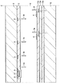
図1は、本実施形態に係る液晶表示基板の第1の例を示す部分断面図である。この図1では、画素の断面の一例を示している。1つの画素(例えば、矩形画素)は、複数のサブピクセルを含むとしてもよい。 FIG. 1 is a partial cross-sectional view showing a first example of a liquid crystal display substrate according to the present embodiment. FIG. 1 shows an example of a cross section of a pixel. One pixel (for example, a rectangular pixel) may include a plurality of subpixels.
本実施形態に係る液晶表示装置の基板1において、表面に樹脂層2が形成されており複数のカラーフィルタ(着色画素)を含む又は含まない対向基板3と、TFTなどの液晶駆動素子が形成されているアレイ基板4とは対向する。互いに対向する対向基板3とアレイ基板4とは、液晶層5を挟持した状態で、貼り合わされる。対向基板3の平面とアレイ基板4の平面とは、それぞれ画素単位又はサブピクセル単位に区分けされる。
In the
さらに、本実施形態に係る基板1は、画素電極である第1の電極6と、液晶駆動時にこの第1の電極とは電位の異なる第2の電極7と、対向基板3の基板(透明基板)8上に透明導電膜などで形成される第3の電極9とを具備する3極の電極構成を持つ。基板1を備える液晶表示装置は、3極の電極構成による斜め電界技術を採用する。
Furthermore, the
第1の電極6は、TFTなどアクティブ素子と電気的に接続され、櫛歯状パターン(ストライプ状でもよい)に形成される。
The
第2の電極7及び第3の電極9は、第1の電極と同様に、櫛歯状パターンに形成される。第2の電極7と第3の電極9との両方又は片方は、共通電極(コモン)としてもよい。図1では、第1から第3の電極6,7,9における櫛歯軸方向(例えば、櫛歯の長手方向、又は、単に、櫛歯方向)に対する垂直断面が図示されている。ここで、櫛歯軸方向とは、例えば、アレイ基板4又は対向基板3を平面視した場合の、第1の電極6、第2の電極7、第3の電極9の線状導体部の長手方向を意味する。アレイ基板4の基板(透明基板)12の表面には、絶縁層10a,10bが形成される。絶縁層10bの上には、第2の電極7が形成される。第2の電極7の上には、絶縁層10cが形成される。絶縁層10cの上には、第1の電極6が形成される。第1の電極6と第2の電極7とは、アレイ基板4と対向基板3との対向方向(厚み方向、高さ方向、垂直方向、又は積層方向でもよい)において絶縁層10cにより電気的に絶縁される。絶縁層10cがSiNx(窒化ケイ素)の場合、この絶縁層10cの実用的な膜厚の範囲は、例えば0.1μmから0.5μmである。
Similar to the first electrode, the
本実施形態においては、例えば、画素又はサブピクセルごとの第3の電極9の櫛歯の数は、第1の電極6の櫛歯の数より多くしてもよい。画素又はサブピクセルごとの第3の電極9の櫛歯の総面積は、第1の電極6の櫛歯の総面積より大きくしてもよい。第1の電極6、第2の電極7、第3の電極9は、可視域において、透明な導電膜とすることができる。各電極6,7,9の櫛歯の密度、ピッチ、及び電極幅は、画素又はサブピクセル内で、適宜調整することができる。画素又はサブピクセルの断面視において、それぞれの電極6,7,9を画素の中心軸から対称となる位置に形成することは、液晶表示の広視野角確保の観点から重要である。それぞれの電極6,7,9を画素の中心軸から対称となる位置に形成するためには、1つの画素又はサブピクセルについて、断面視でそれぞれの電極6,7,9の櫛歯数が2以上かつ偶数であることが必要である。
In the present embodiment, for example, the number of comb teeth of the
さらに、本実施形態において、第1の電極6、第2の電極7、第3の電極9は、向かい合う状態で対向する。本実施形態において、第1の電極6の櫛歯軸方向と、第2及び第3の電極7,9の櫛歯軸方向とは、ほぼ平行となる。そして、本実施形態において、それぞれが対向する第1の電極6の櫛歯の並び位置と、第2の電極の櫛歯7の並び位置とは、対向方向に対して垂直な水平方向(基板8,12の表面に平行な方向)の位置において、第1の方向11aにずれた位置関係となる。また、それぞれが対向する第1の電極6の櫛歯の並び位置と、第3の電極7の櫛歯の並び位置とは、水平方向の位置において、第1の方向11aとは反対の第2の方向11bにずれた位置関係となる。換言すれば、第1の電極6の櫛歯に対して、第2の電極7の櫛歯と第3の電極9の櫛歯とは、それぞれ反対方向にずれた位置関係となる。この図1において、第1の方向11aは画素の中心から画素の端へ向かう方向であり、第2の電極7の櫛歯は、第1の電極6の櫛歯よりも第1の方向11aにずれている。第2の方向11bは画素の端から画素の中心へ向かう方向であり、第3の電極9の櫛歯は、第1の電極6の櫛歯よりも第2の方向11bにずれている。第1から第3の電極6,7,9は、水平方向において、画素の断面の中心軸から対称に形成される。このような第1から第3の電極6,7,9を備えることにより、本実施の形態に係る液晶表示装置は、液晶を効率良く駆動可能である。
Furthermore, in this embodiment, the
対向基板3の基板8上には、対向方向において光を通過させるための開口部を持つブラックマトリクス13が形成され、基板8上の複数のブラックマトリクス13の間(開口部)に、第3の電極9の櫛歯部分が配置される。
On the
ブラックマトリクス13は、例えば、対向する辺が平行な形状を持ち、例えば矩形状であるとする。
The
図2は、本実施形態に係る液晶表示基板1の第2の例を示す部分断面図である。画素又はサブピクセルは、液晶表示の最小単位である。この図2は、第1から第3の電極6,7,9に備えられている各櫛歯軸方向に対する垂直断面を示す。
FIG. 2 is a partial cross-sectional view showing a second example of the liquid
この図2において、アレイ基板4の第1の表面上に少なくとも1層(図2では2層)の絶縁層10a,10bが形成される。絶縁層10b上の特定の位置に第2の電極7が形成される。第2の電極7の形成された絶縁層10b上に少なくとも1層の絶縁層10cが形成される。絶縁層210cの特定の位置に第1の電極6が形成される。
In FIG. 2, at least one (two layers in FIG. 2) insulating
絶縁層10c及び第1の電極6の上に液晶層5が形成される。
A
液晶層5の上に透明樹脂層2が配設される。透明樹脂層2は、上面(液晶層5と逆側の面)の特定の位置に、開口部を持つブラックマトリクス13と、このブラックマトリクス内の第3の電極9とが配設される。本実施形態において、ブラックマトリクス13は、図2の画素の断面の水平方向の両端部に配設される。
The
透明樹脂層2と第3の電極9とブラックマトリクス13との上には、基板8が配設される。
A
図2において、第3の電極9は、画素の断面の中心軸Cから対称に、基板8の液晶層5側の面に配設される。アレイ基板4の基板12上には、絶縁層10a,10bを介して第2の電極7が配設され、さらに、絶縁層10cを介して第1の電極6が配設される。この図2の第2の電極7は、平面視で、ブラックマトリクス13の下の位置、かつ、アレイ基板4側に、ブラックマトリクス13の幅と同程度の幅を持つ部分7aを備える。第2の電極7において、平面視でブラックマトリクス13の下に位置する部分7aは、コモン電位とすることで、隣接の画素又は隣接のサブピクセルへのクロストークを緩和することができる。
In FIG. 2, the
図2において、第1の電極6と第2の電極7とは、水平方向において、画素の断面の中心軸Cから対称に形成される。第2の電極7の櫛歯は、第1の電極6の櫛歯よりも第2の方向11bにずれている。第3の電極9の櫛歯は、第1の電極6の櫛歯よりも第1の方向11aにずれている。
In FIG. 2, the
上記図1及び図2において、対向基板3の基板8上およびアレイ基板4上の基板12上の配向膜、基板1の両面に具備される偏光板などは省略されている。液晶層5は、負の誘電率異方性を有し、初期配向が垂直な液晶分子を含む。垂直配向の液晶層5は、対向基板3とアレイ基板4との間に挟持される。この図1及び図2において、Dは液晶の倒れる方向である。例えば、図1の液晶層5において、液晶分子の軸(長手方向又は長軸方向)は、駆動電圧印加時に、第1の方向11aに倒れ、透過表示可能となる。例えば、図2の液晶層5において、液晶分子の軸は、駆動電圧印加時に、第2の方向11bに倒れ、透過表示可能となる。
1 and 2, the alignment film on the
図3は、第1から第3の電極6,7,9の配置の一例を示す斜視図である。
FIG. 3 is a perspective view showing an example of the arrangement of the first to
第2の電極7の任意の櫛歯7aの水平方向の位置は、この第2の電極7の櫛歯7aに対応する第1の電極6の櫛歯6aの水平方向の位置から、第1の方向11aにずれている。
The horizontal position of an
第3の電極9のある櫛歯9aの水平方向の位置は、この第3の電極9の櫛歯9aに対応する第1の電極6の櫛歯6aの水平方向の位置から、第2の方向11bにずれている。
The horizontal position of the
第1の方向11aと第2の方向11bとは、逆向きである。
The
以下で、画素の1/2の断面図である図4、図5、図6を用いて、液晶層5に含まれる液晶の駆動についてさらに詳細に説明する。
Hereinafter, the driving of the liquid crystal included in the
図4は、駆動電圧無印加時における中心軸Cから左側の画素の一例を示す部分断面図である。 FIG. 4 is a partial cross-sectional view showing an example of a pixel on the left side from the central axis C when no drive voltage is applied.
この図4に示すように、液晶層5の液晶分子5a〜5fは、駆動電圧無印加時に、対向基板3、アレイ基板4のそれぞれの表面(図示しない配向膜の上)に対して垂直に配向する。
As shown in FIG. 4, the
図5は、駆動電圧印加直後における中心軸Cから左側の画素の一例を示す部分断面図である。 FIG. 5 is a partial cross-sectional view showing an example of a pixel on the left side from the central axis C immediately after the drive voltage is applied.
駆動電圧印加直後の対向基板1側では、画素電極である第1の電極6から、共通電極である第3の電極9に向かう電気力線14a〜14dが形成され、液晶分子5a〜5dの軸がこの電気力線14a〜14dの方向に垂直になるように、液晶分子5a〜5dが倒れ始める。
On the
駆動電圧印加直後のアレイ基板4側では、第1の電極6から、共通電極である第2の電極7に向かう電気力線14e,14fが形成され、液晶分子5e,5fの軸がこの電気力線14e,14fの方向に垂直になるように、液晶分子5e,5fが倒れ始める。
On the array substrate 4 side immediately after the drive voltage is applied,
図6は、駆動電圧印加から液晶駆動に十分な所定時間経過後における中心軸Cから左側の画素の一例を示す部分断面図である。 FIG. 6 is a partial cross-sectional view showing an example of a pixel on the left side from the central axis C after a predetermined time sufficient for driving the liquid crystal after applying the driving voltage.
液晶分子5a〜5dの傾きの変化は、電圧の大きさに応じて止まる。図6に示されるように、それぞれの液晶分子5a〜5fは、第1の電極6からの距離に基づいて、傾斜が異なる。さらに、画素は中心軸Cを基準に対称となる。したがって、液晶分子の傾斜及び画素の対称構成によって、駆動電圧印加時の液晶分子に異なる傾きを持たせることができ、液晶表示の視野を拡げることができる。
The change in the inclination of the
以下で、第1から第3の電極6,7,9と液晶動作との関係を図7及び図8を用いて説明する。
Hereinafter, the relationship between the first to
図7は、左側の矩形画素の一例を示す部分断面図である。 FIG. 7 is a partial cross-sectional view illustrating an example of the left rectangular pixel.
図8は、右側の矩形画素の一例を示す部分断面図である。 FIG. 8 is a partial cross-sectional view illustrating an example of the right rectangular pixel.
この図7及び図8に示されるように、液晶層5の液晶分子5g〜5jの倒れる方向は、第2の電極7及び第3の電極9を、第1の電極6に対してずらす方向によって設定可能である。例えば、第1の電極6と第2の電極7との間の水平方向のはみ出し幅W1は、液晶セルのディメンション又は液晶駆動電圧などとの関係で適宜調整される。例えば、画素幅又はピクセル幅が10μmから300μmの場合、はみ出し幅W1は、0.5μmから6μm前後であればよい。はみ出し幅W1は、液晶の応答性を向上させるために、液晶層5の厚みより小さくすることができる。
As shown in FIGS. 7 and 8, the direction in which the
また、第1の電極6と第2の電極7との間の水平方向の重なり幅W2は、補助容量に用いる観点から、液晶セル(画素又はサブピクセル)の電気容量の大きさに基づいて調整される。
Further, the horizontal overlap width W2 between the
第1の電極6の幅W3は、用いられる液晶層5の材料、液晶セル条件、駆動条件などに基づいて適宜調整される。第2及び第3の電極7,9の幅についても、液晶セル条件にしたがって調整される。第1の電極の幅W3は、画素サイズ又はサブピクセルサイズに対応させて2μmから20μmの範囲で調整される。第1の電極6の櫛歯の中心と、第3の電極9の櫛歯の中心との間の距離W4は、例えば液晶セルのディメンション又は用いられる液晶配向の特性などのような液晶セル条件に基づいて適宜調整される。距離W4は、例えば、2μmから30μmの範囲内に設定される。
The width W3 of the
第1の電極6と第2の電極7の重なり幅W2の部分は、補助容量として使用できる。
The portion of the overlapping width W2 between the
第1の電極6の液晶セル内での形成位置と本数とのうちの少なくとも一方に基づいて、はみ出し幅W1、重なり幅W2は、一画素内で変更されてもよい。一画素にTFT素子が複数形成され、複数のTFT素子のそれぞれに対する駆動電圧を変えることによって液晶層5の液晶分子が駆動されるとしてもよい。液晶表示の焼き付きを緩和するために、第1の電極6又は第2の電極7などに印加される駆動電圧にオフセット(電圧シフト)を用いてもよい。例えば、1つの画素又は1つのサブサブピクセルを、2個以上のアクティブ素子によって駆動する場合などにおいては、一方のアクティブ素子の駆動電圧のタイミング又は印加電圧の波形が調整されてもよい。1つの画素又は1つのサブサブピクセルを2個以上のアクティブ素子によって駆動する場合、オフセットは、電圧の大きさがずれるとともに、電圧印加のタイミングもずれるとしてもよい。第2の電極7に印加されるコモン電圧又は第3の電極8に印加されるコモン電圧は、液晶応答性を改善するために、コモン電圧変調としてもよい。
Based on at least one of the formation position and the number of the
一般的な垂直配向液晶は、例えば89度といった傾斜角(プレチルト角)を初期的に持つ。垂直配向液晶は、一般的には、駆動電圧印加時に傾斜角が小さくなる方向に倒れる。一般的な垂直配向液晶では、初期の傾斜角によって駆動電圧印加時の液晶分子の倒れる方向が設定される。このような一般的な垂直配向液晶を用いる場合には、1画素又は1サブピクセルに対して、図示しない配向膜の複数方向のラビング又は複数方向での光配向が必要とされる。 A general vertical alignment liquid crystal initially has a tilt angle (pretilt angle) of 89 degrees, for example. In general, the vertically aligned liquid crystal is tilted in a direction in which the tilt angle decreases when a driving voltage is applied. In a general vertical alignment liquid crystal, an initial tilt angle sets a direction in which liquid crystal molecules are tilted when a driving voltage is applied. When such a general vertical alignment liquid crystal is used, the alignment film (not shown) is rubbed in a plurality of directions or optical alignment in a plurality of directions is required for one pixel or one subpixel.
これに対し、本実施形態では、垂直配向液晶の初期配向に傾斜角を付与することなく、斜め電界で発生される電気力線に基づいて液晶分子の倒れる方向が決められる。本実施形態においては、例えば、負の誘電率異方性の液晶を用いて、液晶の初期配向をおよそ90°の垂直配向としている。上述したように、本実施形態においては、液晶にプレチルト角を付与することは必要ない。しかしながら、液晶駆動において数msの超高速応答を実現するために、PSA法を用いて、液晶に例えば89.7°から88°前後のプレチルト角が付与されてもよい。このように液晶にわずかなプレチルト角を付与することにより、本実施形態に係る液晶表示装置は、超高速応答又は従来よりも低い駆動電圧による液晶駆動を実現することができる。PSA法では、感光性の配向膜又は重合組成物を用いて液晶セル化が実行された後に、第1の電極等に駆動電圧を印加しながら紫外線などの光が液晶に照射され、配向膜又は液晶セル内壁に、プレチルト角が付与される。この配向膜又は液晶セル内壁のプレチルト角に応じて、液晶分子にプレチルト角が付与される。 On the other hand, in this embodiment, the direction in which the liquid crystal molecules fall is determined based on the electric lines of force generated by the oblique electric field without giving an inclination angle to the initial alignment of the vertically aligned liquid crystal. In the present embodiment, for example, liquid crystal having negative dielectric anisotropy is used, and the initial alignment of the liquid crystal is set to a vertical alignment of about 90 °. As described above, in the present embodiment, it is not necessary to give a pretilt angle to the liquid crystal. However, a pretilt angle of, for example, about 89.7 ° to 88 ° may be imparted to the liquid crystal using the PSA method in order to realize an ultrafast response of several ms in the liquid crystal drive. Thus, by providing a slight pretilt angle to the liquid crystal, the liquid crystal display device according to the present embodiment can realize liquid crystal driving with an ultrafast response or a driving voltage lower than that of the conventional one. In the PSA method, after forming a liquid crystal cell using a photosensitive alignment film or a polymerization composition, light such as ultraviolet rays is applied to the liquid crystal while applying a driving voltage to the first electrode or the like, and the alignment film or A pretilt angle is given to the inner wall of the liquid crystal cell. A pretilt angle is given to the liquid crystal molecules according to the pretilt angle of the alignment film or the inner wall of the liquid crystal cell.
本実施形態において、液晶の初期配向は、垂直配向としてもよく、水平配向としてもよい。本実施形態に係る液晶表示装置は、ノーマリーブラック表示の液晶表示装置であってもよく、ノーマリーホワイトの液晶表示装置であってもよい。本実施形態に係る液晶表示装置は、上述したように、カラーフィルタなどを含む対向基板と、TFTなどのような液晶駆動素子が形成されているアレイ基板4とを対向させ、対向基板3とアレイ基板4との間に液晶層5が挟持される構成を持つとしてもよい。液晶の初期配向が水平配向の場合、液晶は、電圧印加時に水平方向から垂直方向に向かって立ち上がる。液晶の初期配向が垂直配向の場合、液晶分子は、電圧印加時に垂直方向から水平方向に倒れる。このように、液晶層5には、誘電率異方性が負である液晶と、正である液晶のどちらを用いてもよい。例えば、誘電率異方性が負の液晶として、室温付近で屈折率異方性が0.08から0.16の範囲のネマチック液晶を用いることができる。液晶応答を高速化するために、液晶厚みを3μm以下とする場合には、例えばΔnが0.1から0.16の範囲の液晶など、屈折率異方性の高い液晶を用いることができる。誘電率異方性が正の液晶が用いられる場合、さらに広範囲の特性を持つ液晶材料を適用することができる。例えば、後述されるように、液晶材料として、分子構造内にフッ素原子を含む液晶材料(以下、フッ素系液晶と称する)を用いることができる。第1の電極6と、第2の電極7のはみ出し部との間には、液晶駆動電圧の印加時に、実質的に強電界が発生する。このため、従来から用いられている垂直配向の液晶材料よりも、低誘電率(誘電率異方性の小さな)の液晶材料を使用することができ、低電圧で液晶を駆動させることができる。高い透過率又は低い飽和電圧を目的として、液晶層5をやや厚めにしても、第2の電極7のはみ出し部に対応する液晶が高速で応答するために、従来の液晶駆動よりも低電圧の液晶駆動又は高速の液晶駆動を実現することができる。一般的に、誘電率異方性の小さな液晶材料は、その粘土が低い。低粘度の液晶材料を用いることにより、駆動電圧をオフした場合の立ち下がり時間(τdecay)を短くすることができる。さらに、誘電率の低いフッ素系液晶においては、イオン性不燃物の取り込みが少なく、不純物による電圧保持率低下などの性能劣化又は表示の焼き付きが小さく、表示ムラが生じにくい。誘電率異方性の絶対値の大きい液晶材料を用いることによって、しきい値電圧又は立ち上がり時間(τrise)を小さくすることができる。誘電率異方性の絶対値の大きい液晶材料が用いられる場合、液晶の低粘度のために、例えばアルケニケル化合物のような減粘剤が液晶に少量添加されてもよい。液晶層5の厚みは、特に限定されない。例えば、液晶層5の厚さとして、超高速応答の液晶表示を実現するために、3.5μm以下、好ましくは1.5μmから3.4μmの範囲の薄い厚さが適用されてもよい。本実施形態では、第1から第3の電極6,7,9によって、斜め電界とはみ出し構造とが併用される。このような本実施形態においては、液晶粘度とその比誘電率、複屈折率、弾性定数を最適化し、液晶表示装置の消費電力を従来よりも低下させることができる。本実施形態で実効的に適用可能な液晶層5のΔndは、例えば、およそ200nmから500nmの範囲である。上記図1〜図8で省略されている配向膜としては、例えば、ポリイミド系有機高分子膜、又はポリシロキサン構造を含む有機高分子膜を加熱硬膜化して用いることができる。また、液晶表示装置において、例えば、1から3枚の位相差板を偏光板に貼り合わせて用いてもよい。
In the present embodiment, the initial alignment of the liquid crystal may be vertical alignment or horizontal alignment. The liquid crystal display device according to the present embodiment may be a normally black liquid crystal display device or a normally white liquid crystal display device. As described above, in the liquid crystal display device according to the present embodiment, the counter substrate including the color filter and the array substrate 4 on which the liquid crystal driving elements such as TFTs are formed are opposed to each other. The
以下で、第1から第3の電極6,7,9の平面配置状態の例について図9から図11を用いて説明する。図9から図11では、例えば、第3の電極9の垂直方向の配置状態を例として説明する。
Hereinafter, an example of a planar arrangement state of the first to
図9は、第3の電極9の第1の例を示す上平面図である。
FIG. 9 is an upper plan view showing a first example of the
第3の電極9は、平面の形状が矩形状の画素15に対して備えられている。第3の電極9は、櫛歯状である。第3の電極9の櫛歯軸方向は、平面において、画素15のいずれかの辺と平行である。第3の電極9は、対向基板3の基板8の液晶側の平面に対して、ほぼ平行に備えられる。
The
なお、第2の電極7は、第1の電極6の下側に、第1の電極6と間隔を空けて、平行に配置される。第3の電極9は、第1の電極6の上側に、第1の電極6の間隔を空けて、平行に配置される。以下の図10及び図11の場合も同様である。
Note that the
図10は、第3の電極9の第2の例を示す上平面図である。
FIG. 10 is an upper plan view showing a second example of the
この図10において、平面の形状が矩形状の画素15は、平面において、水平方向の中心線C1及び垂直方向の中心線C2により4つの分割領域に分割されており、各分割領域のそれぞれに櫛歯状の第3の電極9が備えられている。各第3の電極9における櫛歯軸方向は、中心線C1又は中心線C2、あるいは、画素のいずれかの辺に平行である。中心線C1,C2の交わる中心点において、4つの分割領域の4つの第3の電極9は、点対称の関係を持つ。分割領域同士の間でいずれかの辺が接する場合、この辺が接する分割領域の第2の電極9の櫛歯軸方向は異なるとしてもよい。すなわち、4つの第3の電極9には、櫛歯軸方向が異なる電極が含まれていてもよい。
In FIG. 10, a
図11は、第3の電極9の第3の例を示す上平面図である。この図11において、第3の電極9の櫛歯軸方向は、各画素又は各分割領域の各辺と平行ではない関係を持つ。
FIG. 11 is an upper plan view showing a third example of the
この図11では、平面の形状が矩形状の画素15が、平面における水平方向の中心線C1及び垂直方向の中心線C2により4つの分割領域に分割されている。1つの画素15に対して、2つの第3の電極9が割り当てられる。2つの第3の電極9のうちの一方は、画素15の右側に設置され、他方は、画素15の左側に設置される。2つの第3の電極9における櫛歯軸方向は、中心線C1及び中心線C2に対して傾きを持つ。すなわち、櫛歯軸方向は、平面における水平方向の中心線C1及び垂直方向の中心線C2と、平行及び垂直でない。中心線C1,C2の交わる中心点において、2つの第3の電極9は、点対称の関係を持つ。
In FIG. 11, a
上記図10及び図11では、複数の液晶ドメインを形成するために、画素15が複数の領域に分けられている。そして、この複数の領域における櫛歯軸方向を変えることで、視野角を拡大することができる。
10 and 11, the
なお、上記図9から図11において、第1の電極6及び第2の電極7についても、上記の第3の電極9と同様の配置状態を用いることができる。例えば、第2の電極7は、第1の電極6の下側に、第1の電極6と間隔を空けて、平行に配置される。第3の電極9は、第1の電極6の上側に、第1の電極6の間隔を空けて、平行に配置される。
9 to 11, the same arrangement state as the
第2の電極7の櫛歯及び第3の電極9の櫛歯は、櫛歯軸方向に垂直な断面において、基板8,12と平行な方向(水平方向)に対する配置に関して、それぞれが第1の電極6からずれている。櫛歯軸方向に垂直な断面において、第1の電極6から第2の電極7へ向かう水平方向のずれは、第1の電極6から第3の電極9へ向かう水平方向のずれと、反対となる。
The comb teeth of the
上記の第1から第3の電極6,7,9は、画素15単位で形成される場合を例として説明した。しかしながら、例えば、上記の第1から第3の電極6,7,9を、サブピクセル単位で形成するとしてもよい。
The first to
画素又はサブピクセルの平面形状は、上記図9から図11では、矩形状としているが、他の形状を用いてもよい。画素の平面形状としては、例えば、平行四辺形などのような対向する辺が平行な形状とすることができる。 The planar shape of the pixel or subpixel is rectangular in FIGS. 9 to 11, but other shapes may be used. As the planar shape of the pixel, for example, the opposing sides such as a parallelogram can be parallel.
ブラックマトリクス13は、液晶表示のコントラストをアップさせるために、表示の最小単位である画素又はサブピクセルの周囲、あるいは画素の両辺に配設される遮光性のパターンである。
The
矩形画素は、ブラックマトリクス13の開口部に対応し、「絵素」と同義である。
The rectangular pixel corresponds to the opening of the
アレイ基板12側の第1の電極6及び第2の電極7の材料としては、上述したITOなどのような、導電性の金属酸化物を用いることができる。また、第1の電極6及び第2の電極7の材料として、金属酸化物より導電性の高い金属が用いられてもよい。反射型又は半透過型の液晶表示装置の場合には、第1の電極6と第2の電極7のうちの少なくとも一方の材料として、アルミニウム又はアルミニウム合金の薄膜を用いてもよい。アルミニウム又はアルミニウム合金の薄膜が用いられる場合、これらの薄膜表面に酸化アルミニウムを保護層として形成してもよい。
As a material of the
第1の電極6、第2の電極7、及び上記図1から図11で省略されているアクティブ素子の金属配線などは、窒化ケイ素(SiNx)又は酸化ケイ素(SiOx)などの絶縁層10a〜10cのうちの少なくとも一つを介して形成される。上記の図1から図11では、TFT素子やTFT素子に接続される金属配線は省略されている。なお、導電性金属酸化物であるITOとの低コンタクト性を有するアルミニウム合金の単層によりゲート配線及びソース配線をそれぞれで形成する技術は、例えば、特開2009−105424号公報に開示されている。
The
本実施形態に係る液晶表示基板1は、対向基板3とTFTのアクティブ素子が形成されているアレイ基板4とを貼り合わせた構成である。対抗基板3とアレイ基板4との間には、液晶層5が封入される。
The liquid
アレイ基板4には、櫛歯状又はストライプ状の第1及び第2の電極6,7を備えており、対向基板3は、櫛歯状又はストライプ状の第3の電極9を備える。
The array substrate 4 is provided with first and
本実施形態に係る液晶表示装置は、さらに、基板1の両面に、偏光板及び位相差板を備える。これにより、本実施形態に係る液晶表示装置は、モノクロで階調表示可能である。対向基板3及びアレイ基板4の表面には、予め垂直配向膜が塗布、形成されているとしてもよい。なお、垂直配向用の配向膜は、本実施形態において図示を省略している。本実施形態では、MVA又はVATNなどの垂直配向の液晶表示装置に必要な厳密な配向処理(例えば、チルト角89°とし、複数ドメインを形成するための複数方向の配向処理)を実施する必要がなく、液晶のチルト角はほぼ90°の垂直配向とすることができる。
The liquid crystal display device according to this embodiment further includes a polarizing plate and a retardation plate on both surfaces of the
初期配向が垂直配向の液晶分子は、駆動電圧印加時に、第1の電極6と第2の電極7との間に生じる電気力線(電界)により、また、第1の電極6と第3の電極9との間の斜め電界により、この斜め電界と垂直になるように倒れ始める。
The liquid crystal molecules whose initial alignment is vertical alignment are generated by electric lines of force (electric field) generated between the
本実施形態において、第2の電極7と第3の電極9とは、第1電極6から反対方向にずれている。第3の電極9と第2の電極7とは、例えば、同電位でもよい。画素電極である第1の電極6は、TFTであるアクティブ素子のドレインと電気的に接続されるとしてもよい。本実施形態において、TFT及び垂直配向膜は、図示することを省略している。
In the present embodiment, the
以上説明した本実施形態に係る液晶表示装置においては、ディスクリネーションを軽減することができ、視野角を広くすることができ、画面を明るくすることができる。 In the liquid crystal display device according to this embodiment described above, disclination can be reduced, the viewing angle can be widened, and the screen can be brightened.
本実施形態においては、斜め電界により効果的な液晶駆動を行うことができ、液晶の応答性を向上させることができる。 In the present embodiment, effective liquid crystal driving can be performed by an oblique electric field, and the response of the liquid crystal can be improved.
なお、本実施形態において、対向基板3は、例えば、基板8と、基板8上に形成された第3の電極9と、第3の電極9の形成された透明基板8上に形成されたブラックマトリクス13と、第3の電極9及びブラックマトリクス13の形成された基板3上に形成された透明樹脂層2とを具備する構成としてもよい。
In the present embodiment, the
対向基板3は、例えば、基板8と、基板8上に形成されたブラックマトリクス13と、ブラックマトリクス13の形成された基板8上に形成された透明樹脂層2と、透明樹脂層2上であり、ブラックマトリクス13の開口部に対応する位置に形成された第3の電極9とを具備する構成としてもよい。
The
(第2の実施形態)
本実施形態においては、ブラックマトリクスの開口部にカラーフィルタを備える対向基板(カラーフィルタ基板)について説明する。(Second Embodiment)
In the present embodiment, a counter substrate (color filter substrate) including a color filter in an opening of a black matrix will be described.
図12は、本実施形態に係る液晶表示基板の一例を示す断面図である。 FIG. 12 is a cross-sectional view showing an example of a liquid crystal display substrate according to this embodiment.
本実施形態に係る液晶表示基板16において、対向基板17と、アレイ基板4とは互いに対向する。対向基板17とアレイ基板4とは、液晶層5を挟持し、貼り合わされる。
In the liquid
より具体的に説明すると、アレイ基板4の上面に液晶層5が配設される。液晶層5の上面に第3の電極9が配設される。液晶層5及び第3の電極9の上面に、透明樹脂層2が配設される。透明樹脂層2の上面に、カラーフィルタ18及びブラックマトリクス13が配設される。カラーフィルタ18は、例えば、赤フィルタ18r、緑フィルタ18g、青フィルタ18bを含む。カラーフィルタ18及びブラックマトリクス13の上面には、基板8が配設される。この図12においては、平面視で、ブラックマトリクス13と重なる位置に、第3の電極9の櫛歯、第2の電極7の櫛歯が設けられている。
More specifically, the
図13は、カラーフィルタを備えた対向基板の一例を示す断面図である。 FIG. 13 is a cross-sectional view illustrating an example of a counter substrate including a color filter.
対向基板17の基板8上には、開口部を持つブラックマトリクス13と、少なくとも開口部におけるカラーフィルタ18が形成される。カラーフィルタ18の上には、透明樹脂層2が形成される。透明樹脂層2の上には、第3の電極9が形成される。
On the
図14は、駆動電圧印加直後における画素の一例を示す部分断面図である。 FIG. 14 is a partial cross-sectional view illustrating an example of a pixel immediately after application of a drive voltage.
垂直配向の液晶層5の液晶5k〜5pは、駆動電圧無印加時に、対向基板17、アレイ基板4のそれぞれの表面(図示しない配向膜上)に対して垂直に配向する。駆動電圧印加直後においては、画素電極である第1の電極6から第3の電極9に向かう電気力線14k〜14pが形成され、液晶5k〜5pの軸がこの電気力線14k〜14pの方向に垂直になるように、液晶5k〜5pが倒れ始める。
The
図15は、駆動電圧印加から所定時間経過後における画素の一例を示す部分断面図である。 FIG. 15 is a partial cross-sectional view illustrating an example of a pixel after a predetermined time has elapsed since the application of the drive voltage.
液晶5k〜5pの傾きの変化は、電圧の大きさに応じて止まる。図15に示されるように、それぞれの液晶5k〜5pは、第1の電極6からの距離に基づいて、傾斜が異なる。したがって、第1から第3の電極6,7,9に対する電圧印加に応じて、駆動電圧印加時の液晶5k〜5pに異なる傾きを持たせることができ、液晶表示の視野を拡げることができる。
The change in the inclination of the
本実施形態において、対向基板17は、例えばブラックマトリクス13の形成材料として、遮光層を備えるとしてもよい。また、対向基板17は、例えばブラックマトリクス13の形成材料、カラーフィルタ18の形成材料として、着色層とを備えるとしてもよい。遮光層とは、透明樹脂に遮光性の顔料を分散させた遮光性の塗膜である。遮光層には、一般的に感光性が付与される。遮光層は、露光・現像を含むフォトリソグラフィの手法によりパターン形成される。着色層とは、後述される有機顔料を透明樹脂に分散させた塗膜である。着色層は、ブラックマトリクス開口部への塗膜の形成、フォトリソグラフィ法によるパターン形成により、形成される。
In the present embodiment, the
本実施形態において、着色層の比誘電率は、比較的重要な特性である。この着色層の比誘電率は、透明樹脂に対する着色剤として添加される有機顔料の比率に基づいてほぼ一義的に決定される。このため、比誘電率を大きく変化させることは困難である。換言すれば、着色層中の有機顔料の種類又は含有量は、液晶表示装置として必要な色純度から設定され、これにより着色層の比誘電率もほぼ決まる。なお、有機顔料の比率を高くして着色層を薄膜化することにより、比誘電率を4以上とすることが可能である。また、透明樹脂として高屈折率材料を用いることにより、比誘電率を若干アップ可能である。有機顔料を用いた着色層の比誘電率は、概ね2.9から4.5の範囲に入る。 In the present embodiment, the relative dielectric constant of the colored layer is a relatively important characteristic. The relative dielectric constant of the colored layer is almost uniquely determined based on the ratio of the organic pigment added as a colorant to the transparent resin. For this reason, it is difficult to change the relative dielectric constant greatly. In other words, the type or content of the organic pigment in the colored layer is set based on the color purity required for the liquid crystal display device, and the relative dielectric constant of the colored layer is almost determined accordingly. The relative dielectric constant can be increased to 4 or more by increasing the ratio of the organic pigment and making the colored layer thin. In addition, the relative dielectric constant can be slightly increased by using a high refractive index material as the transparent resin. The relative dielectric constant of the colored layer using the organic pigment is approximately in the range of 2.9 to 4.5.
カラーフィルタ18に含まれる着色画素フィルタは、赤フィルタ18r、緑フィルタ18g、青フィルタ18bの3色を含むとしてもよく、黄フィルタなどの補色系フィルタを含むとしてもよく、白色画素(透明画素)を含むとしてもよい。カラーフィルタ18は、対向基板17側に備えるのではなく、アレイ基板4上に備えるとしてもよい。また、カラーフィルタを用いることなく、赤・緑・青の個別発光素子を備えるバックライトを用いるとしてもよい。例えば、本実施形態に係る液晶表示装置は、LEDバックライトを備えており、時分割発光(フィールド・シーケンシャル)を用いるカラー液晶表示装置であるとしてもよい。
The colored pixel filter included in the
以下で、画素の上平面の形状及び配列の例について図16から図20を用いて説明する。 Hereinafter, an example of the shape and arrangement of the upper plane of the pixel will be described with reference to FIGS.
図16は、3つのサブピクセルを含む1画素の上平面の形状及び配列の一例を示す平面図である。 FIG. 16 is a plan view showing an example of the shape and arrangement of the upper plane of one pixel including three subpixels.
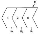
この図16では、縦ストライプカラーフィルタが示されている。矩形(長方形又は正方形)の画素19は、矩形の赤サブピクセル19r、矩形の緑サブピクセル19g、矩形の青サブピクセル19bにより構成されている。
In FIG. 16, a vertical stripe color filter is shown. The rectangular (rectangular or square)
図17は、向かい合う辺が平行な多角形の複数のサブピクセル19r,19g,19bを含む1画素19の上平面の形状及び配列の一例を示す平面図である。
FIG. 17 is a plan view showing an example of the shape and arrangement of the upper plane of one
この図17では、横ストライプカラーフィルタが示されている。縦方向のラインは波形状となる。9つの平行四辺形状の赤サブピクセル19rが行方向(横方向)に配列されている。赤サブピクセル19rの下行に、9つの平行四辺形状の緑サブピクセル19gが行方向に配列されている。緑サブピクセル19gの下に、9つの平行四辺形状の青サブピクセル19gが行方向に配列されている。画素19は、9つの赤サブピクセル19r、9つの緑サブピクセル19g、9つの青サブピクセル19bにより構成されている。
In FIG. 17, a horizontal stripe color filter is shown. The vertical line has a wave shape. Nine parallelogram-shaped
図17では、隣り合う上下の行の間で斜辺の傾きが異なる。すなわち、上下に配列される2つの平行四辺形のサブピクセルは、接線に対して対称となり、「<」形状(又は、アローヘッド型、「V」字を90度回転させた型)に配置される。赤サブピクセル19rと、2行下の赤サブピクセル19rとは、緑サブピクセル19gと青サブピクセル19bとを挟んで、斜辺の角度が異なる。緑サブピクセル19gと、2行下の緑サブピクセル19gとは、青サブピクセル19bと赤サブピクセル19rとを挟んで、斜辺の角度が異なる。青サブピクセル19bと、2行下の青サブピクセル19bとは、赤サブピクセル19rと緑サブピクセル19gとを挟んで、斜辺の角度が異なる。
In FIG. 17, the slope of the hypotenuse differs between adjacent upper and lower rows. That is, two parallelogram sub-pixels arranged vertically are symmetrical with respect to the tangent and are arranged in a “<” shape (or an arrow head type, a type in which the “V” character is rotated 90 degrees). The The
図18は、複数の平行四辺形状のサブピクセル19r,19g,19bを含む縦ストライプの画素19の上平面の形状及び配列の一例を示す平面図である。縦方向のラインは、波形状になる。
FIG. 18 is a plan view showing an example of the shape and arrangement of the upper plane of the vertically striped
この図18では、行方向に、赤サブピクセル19r、緑サブピクセル19g、青サブピクセル19bが配列されており、各列方向(縦方向)に、複数の赤サブピクセル19r、複数の緑サブピクセル19g、複数の青サブピクセル19bが配列されている。
In FIG. 18, a
図19は、複数の平行四辺形状のサブピクセル19r,19g,19bを含む横ストライプの画素19の上平面の形状及び配列の一例を示す平面図である。
FIG. 19 is a plan view showing an example of the shape and arrangement of the upper plane of the
上記のような平行四辺形の画素又はサブピクセルにおいて、第1から第3の電極6,7,9の櫛歯方向は、上辺又は下辺に平行でもよく、斜辺に平行でもよい。
In the parallelogram pixel or sub-pixel as described above, the comb tooth directions of the first to
この図19では、上記図17の場合と同様に、各行方向に、複数の赤サブピクセル19r、複数の緑サブピクセル19g、複数の青サブピクセル19bが配列されており、縦方向に、赤サブピクセル19r、緑サブピクセル19g、青サブピクセル19bが配列されている。
In FIG. 19, as in FIG. 17, a plurality of red sub-pixels 19r, a plurality of green sub-pixels 19g, and a plurality of blue sub-pixels 19b are arranged in each row direction, and the red sub-pixels are arranged in the vertical direction.
図20は、1単位で「<」形状が形成されるサブピクセル19r,19g,19b及び画素19の上平面の形状及び配列の一例を示す平面図である。
FIG. 20 is a plan view showing an example of the shape and arrangement of the upper planes of the
このように、「<」形状のサブピクセル19r,19g,19bにより、画素19が構成されるとしてもよい。複数の画素19は、横ストライプ配列でもよく、縦ストライプ配列でもよい。
In this manner, the
上記のような「<」形状の画素又はサブピクセルにおいて、第1から第3の電極6,7,9の櫛歯方向は、画素又はサブピクセルのいずれかの辺に平行とすることができる。
In the “<” shaped pixel or subpixel as described above, the comb tooth directions of the first to
以上説明した本実施形態に係るカラーフィルタ18を備えた液晶表示基板16においては、ディスクリネーションを軽減することができ、視野角を広くすることができ、画面を明るくすることができる。
In the liquid
本実施形態に係る基板16を用いることにより、斜め電界により効果的な液晶駆動を行うことができ、液晶の応答性を向上させることができる。
By using the
本実施形態のように、画素19及びサブピクセル19r,19g,19bの形状は、自由に設定することができ、これにより液晶の配向を変化させることができ、広い視野角を実現させることができる。
As in the present embodiment, the shape of the
なお、本実施形態において、対向基板17は、基板8と、基板8上に形成された第3の電極9と、第3の電極9の形成された基板8上に形成されたブラックマトリクス13と、ブラックマトリクス13の開口部に形成されたカラーフィルタ18と、カラーフィルタ18上に形成された透明樹脂層2とを具備する構成としてもよい。
In the present embodiment, the
対向基板17は、例えば、基板8と、基板8上に形成されたブラックマトリクス13と、ブラックマトリクス13の開口部に形成された第3の電極9と、第3の電極9の形成されたブラックマトリクス13の開口部に形成されたカラーフィルタ18と、カラーフィルタ18上に形成された透明樹脂層2とを具備する構成としてもよい。
The
(第3の実施形態)
本実施形態においては、上記第2の実施形態で説明したカラーフィルタ18に使用可能な透明樹脂及び有機顔料等の例について説明する。(Third embodiment)
In the present embodiment, examples of transparent resins and organic pigments that can be used for the
[透明樹脂]
遮光層又は着色層の形成に用いられる感光性着色組成物は、顔料分散体に加え、多官能モノマー、感光性樹脂又は非感光性樹脂、重合開始剤、溶剤等を含む。以下、感光性樹脂及び非感光性樹脂など、本実施形態で使用可能な透明性の高い有機樹脂を総称して透明樹脂と呼ぶ。[Transparent resin]
The photosensitive coloring composition used for forming the light-shielding layer or the colored layer contains a polyfunctional monomer, a photosensitive resin or a non-photosensitive resin, a polymerization initiator, a solvent and the like in addition to the pigment dispersion. Hereinafter, highly transparent organic resins that can be used in this embodiment, such as a photosensitive resin and a non-photosensitive resin, are collectively referred to as a transparent resin.
透明樹脂は、熱可塑性樹脂、熱硬化性樹脂、又は感光性樹脂を含む。熱可塑性樹脂としては、例えば、ブチラール樹脂、スチレンーマレイン酸共重合体、塩素化ポリエチレン、塩素化ポリプロピレン、ポリ塩化ビニル、塩化ビニル−酢酸ビニル共重合体、ポリ酢酸ビニル、ポリウレタン系樹脂、ポリエステル樹脂、アクリル系樹脂、アルキッド樹脂、ポリスチレン樹脂、ポリアミド樹脂、ゴム系樹脂、環化ゴム系樹脂、セルロース類、ポリブタジエン、ポリエチレン、ポリプロピレン、ポリイミド樹脂等が用いられる。熱硬化性樹脂としては、例えば、エポキシ樹脂、ベンゾグアナミン樹脂、ロジン変性マレイン酸樹脂、ロジン変性フマル酸樹脂、メラミン樹脂、尿素樹脂、フェノール樹脂等が用いられる。熱硬化性樹脂としては、例えば、メラミン樹脂とイソシアネート基を含有する化合物とを反応させて得られる物質が使用されてもよい。 The transparent resin includes a thermoplastic resin, a thermosetting resin, or a photosensitive resin. Examples of the thermoplastic resin include butyral resin, styrene-maleic acid copolymer, chlorinated polyethylene, chlorinated polypropylene, polyvinyl chloride, vinyl chloride-vinyl acetate copolymer, polyvinyl acetate, polyurethane resin, and polyester resin. Acrylic resins, alkyd resins, polystyrene resins, polyamide resins, rubber resins, cyclized rubber resins, celluloses, polybutadiene, polyethylene, polypropylene, polyimide resins, and the like are used. As the thermosetting resin, for example, epoxy resin, benzoguanamine resin, rosin-modified maleic acid resin, rosin-modified fumaric acid resin, melamine resin, urea resin, phenol resin and the like are used. As the thermosetting resin, for example, a substance obtained by reacting a melamine resin and a compound containing an isocyanate group may be used.
[アルカリ可溶性樹脂]
本実施形態で使用されるブラックマトリクス13の形成材料である遮光層、着色層の形成には、フォトリソグラフィによるパターン形成可能な感光性樹脂組成物を用いることが好ましい。透明樹脂は、アルカリ可溶性を付与された樹脂であることが好ましい。アルカリ可溶性樹脂としては、カルボキシル基又は水酸基を含む樹脂を使用することができる。例えば、アルカリ可溶性樹脂として、エポキシアクリレート系樹脂、ノボラック系樹脂、ポリビニルフェノール系樹脂、アクリル系樹脂、カルボキシル基含有エポキシ樹脂、カルボキシル基含有ウレタン樹脂等を使用することができる。アルカリ可溶性樹脂としては、エポキシアクリレート系樹脂、ノボラック系樹脂、アクリル系樹脂が好ましく、特に、エポキシアクリレート系樹脂やノボラック系樹脂が好ましい。[Alkali-soluble resin]
It is preferable to use a photosensitive resin composition capable of forming a pattern by photolithography for forming the light shielding layer and the colored layer, which are the forming materials of the
[アクリル樹脂]
透明樹脂としては、例えば、以下のアクリル系樹脂を適用可能である。[acrylic resin]
As the transparent resin, for example, the following acrylic resins are applicable.
アクリル系樹脂には、単量体として、例えば(メタ)アクリル酸;メチル(メタ)アクリレート、エチル(メタ)アクリレート、プロピル(メタ)アクリレート、ブチル(メタ)アクリレート、t−ブチル(メタ)アクリレートペンジル(メタ)アクリレート、ラウリル(メタ)アクリレート等のアルキル(メタ)アクリレート;ヒドロキシエチル(メタ)アクリレート、ヒドロキシプロピル(メタ)アクリレート等の水酸基含有(メタ)アクリレート;エトキシエチル(メタ)アクリレート、グリシジル(メタ)アクリレート等のエーテル基含有(メタ)アクリレート;及びシクロヘキシル(メタ)アクリレート、イソボルニル(メタ)アクリレート、ジシクロペンテニル(メタ)アクリレート等の脂環式(メタ)アクリレート等を用いて得られる重合体が用いられる。 Examples of acrylic resins include (meth) acrylic acid; methyl (meth) acrylate, ethyl (meth) acrylate, propyl (meth) acrylate, butyl (meth) acrylate, and t-butyl (meth) acrylate pen. Alkyl (meth) acrylates such as zil (meth) acrylate and lauryl (meth) acrylate; hydroxyl-containing (meth) acrylates such as hydroxyethyl (meth) acrylate and hydroxypropyl (meth) acrylate; ethoxyethyl (meth) acrylate and glycidyl ( Using ether group-containing (meth) acrylates such as meth) acrylate; and alicyclic (meth) acrylates such as cyclohexyl (meth) acrylate, isobornyl (meth) acrylate, dicyclopentenyl (meth) acrylate, etc. Is the polymer is used.
なお、上記の単量体には、単独の物質を用いてもよく、又は、2種以上の物質を併用してもよい。さらに、単量体と共重合可能なスチレン、シクロヘキシルマレイミド、又はフェニルマレイミド等の化合物との共重合体を、アクリル樹脂に用いてもよい。 In addition, a single substance may be used for said monomer, or 2 or more types of substances may be used together. Furthermore, a copolymer with a compound such as styrene, cyclohexylmaleimide, or phenylmaleimide that can be copolymerized with the monomer may be used for the acrylic resin.
例えば(メタ)アクリル酸等のエチレン性不飽和基を有するカルボン酸を共重合して得られた共重合体と、グリシジルメタクリレート等のエポキシ基及び不飽和二重結合を含有する化合物とを反応させることによって、感光性を有する樹脂を得るとしてもよい。また、グリシジルメタクリレート等のエポキシ基含有(メタ)アクリレートの重合体又はグリシジルメタクリレート等のエポキシ基含有(メタ)アクリレートの重合体と他の(メタ)アクリレートとの共重合体に、(メタ)アクリル酸等のカルボン酸含有化合物を付加させることによって、感光性を有する樹脂を得るとしてもよい。 For example, a copolymer obtained by copolymerizing a carboxylic acid having an ethylenically unsaturated group such as (meth) acrylic acid is reacted with a compound containing an epoxy group and an unsaturated double bond such as glycidyl methacrylate. Thus, a resin having photosensitivity may be obtained. In addition, (meth) acrylic acid is a polymer of an epoxy group-containing (meth) acrylate such as glycidyl methacrylate or a copolymer of an epoxy group-containing (meth) acrylate such as glycidyl methacrylate and another (meth) acrylate. A resin having photosensitivity may be obtained by adding a carboxylic acid-containing compound such as.
例えば、ヒドロキシエチルメタアクリレート等のモノマーであり、水酸基を有する重合体に、メタクリロイルオキシエチルイソシアネート等のイソシアネート基及びエチレン性不飽和基を有する化合物を反応させることによって、感光性を有する樹脂を得るとしてもよい。 For example, it is a monomer such as hydroxyethyl methacrylate, and a photosensitive resin is obtained by reacting a polymer having a hydroxyl group with a compound having an isocyanate group such as methacryloyloxyethyl isocyanate and an ethylenically unsaturated group. Also good.
また、上述したように、複数の水酸基を有するヒドロキシエチルメタクリレート等の共重合体と多塩基酸無水物を反応させて、共重合体にカルボキシル基を導入し、カルボキシル基を有する樹脂を得ることができる。カルボキシル基を有する樹脂の製造方法は、この方法のみに限るものではない。 In addition, as described above, it is possible to react a copolymer such as hydroxyethyl methacrylate having a plurality of hydroxyl groups with a polybasic acid anhydride to introduce a carboxyl group into the copolymer to obtain a resin having a carboxyl group. it can. The method for producing a resin having a carboxyl group is not limited to this method.
上記の反応に用いる酸無水物の例として、例えばマロン酸無水物、コハク酸無水物、マレイン酸無水物、イタコン酸無水物、フタル酸無水物、テトラヒドロフタル酸無水物、ヘキサヒドロフタル酸無水物、メチルテトラヒドロフタル酸無水物、及びトリメリト酸無水物等がある。 Examples of acid anhydrides used in the above reaction include, for example, malonic acid anhydride, succinic acid anhydride, maleic acid anhydride, itaconic acid anhydride, phthalic acid anhydride, tetrahydrophthalic acid anhydride, hexahydrophthalic acid anhydride , Methyltetrahydrophthalic anhydride, and trimellitic anhydride.
上述したアクリル系樹脂の固形分酸価は、20〜180mgKOH/gであることが好ましい。酸価が20mgKOH/gより小さい場合には、感光性樹脂組成物の現像速度が遅すぎて現像に要する時間が多くなり、生産性が劣る傾向がある。また、固形分酸価が180mgKOH/gより大きい場合には、逆に現像速度が速すぎて、現像後でのパターンハガレ又はパターン欠けなどのような不具合が生じる傾向がある。 It is preferable that the solid content acid value of the acrylic resin described above is 20 to 180 mgKOH / g. When the acid value is less than 20 mgKOH / g, the development speed of the photosensitive resin composition is too slow, and the time required for development tends to increase, and the productivity tends to be inferior. On the other hand, when the solid content acid value is larger than 180 mgKOH / g, on the contrary, the development speed is too high, and there is a tendency that problems such as pattern peeling or pattern chipping after development occur.
さらに、上記アクリル系樹脂が感光性を有する場合、このアクリル樹脂の二重結合当量は100以上であることが好ましく、より好ましくは100〜2000であり、最も好ましくは100〜1000である。二重結合当量が2000を超える場合には、十分な光硬化性が得られない場合がある。 Furthermore, when the said acrylic resin has photosensitivity, it is preferable that the double bond equivalent of this acrylic resin is 100 or more, More preferably, it is 100-2000, Most preferably, it is 100-1000. When the double bond equivalent exceeds 2000, sufficient photocurability may not be obtained.
[光重合性モノマー]
光重合性モノマーとして、例えば、2−ヒドロキシエチル(メタ)アクリレート、2−ヒドロキシプロピル(メタ)アクリレート、シクロヘキシル(メタ)アクリレート、ポリエチレングリコールジ(メタ)アクリレート、ペンタエリスリトールトリ(メタ)アクリレート、トリメチロールプロパントリ(メタ)アクリレート、ジペンタエリスリトールヘキサ(メタ)アクリレート、トリシクロデカニル(メタ)アクリレート、メラミン(メタ)アクリレート、エポキシ(メタ)アクリレート等の各種アクリル酸エステルおよびメタクリル酸エステル、(メタ)アクリル酸、スチレン、酢酸ビニル、(メタ)アクリルアミド、N−ヒドロキシメチル(メタ)アクリルアミド、アクリロニトリル等を用いることができる。[Photopolymerizable monomer]
Examples of the photopolymerizable monomer include 2-hydroxyethyl (meth) acrylate, 2-hydroxypropyl (meth) acrylate, cyclohexyl (meth) acrylate, polyethylene glycol di (meth) acrylate, pentaerythritol tri (meth) acrylate, and trimethylol. Various acrylic and methacrylic acid esters such as propane tri (meth) acrylate, dipentaerythritol hexa (meth) acrylate, tricyclodecanyl (meth) acrylate, melamine (meth) acrylate, epoxy (meth) acrylate, (meth) Acrylic acid, styrene, vinyl acetate, (meth) acrylamide, N-hydroxymethyl (meth) acrylamide, acrylonitrile and the like can be used.
また、光重合性モノマーとして、例えば、水酸基を有する(メタ)アクリレートに多官能イソシアネートを反応させて得られる(メタ)アクリロイル基を有する多官能ウレタンアクリレートが用いられることが好ましい。なお、水酸基を有する(メタ)アクリレートと多官能イソシアネートとの組み合わせは任意であり、特に限定されるものではない。また、光重合性モノマーとして、1種の多官能ウレタンアクリレートを単独で用いてもよく、2種以上を組み合わせて用いることもできる。 Moreover, it is preferable that the polyfunctional urethane acrylate which has a (meth) acryloyl group obtained by making polyfunctional isocyanate react with the (meth) acrylate which has a hydroxyl group as a photopolymerizable monomer, for example. The combination of the (meth) acrylate having a hydroxyl group and the polyfunctional isocyanate is arbitrary and is not particularly limited. Further, as the photopolymerizable monomer, one kind of polyfunctional urethane acrylate may be used alone, or two or more kinds may be used in combination.
[光重合開始剤]
光重合開始剤としては、例えば、4−フェノキシジクロロアセトフェノン、4−t−ブチル−ジクロロアセトフェノン、ジエトキシアセトフェノン、1−(4−イソプロピルフェニル)−2−ヒドロキシ−2−メチルプロパン−1−オン、1−ヒドロキシシクロヘキシルフェニルケトン、2−ベンジル−2−ジメチルアミノ−1−(4−モルフォリノフェニル)−ブタン−1−オン等のアセトフェノン系化合物;ベンゾイン、ベンゾインメチルエーテル、ベンゾインエチルエーテル、ベンゾインイソプロピルエーテル、ベンジルジメチルケタール等のベンゾイン系化合物;ベンゾフェノン、ベンゾイル安息香酸、ベンゾイル安息香酸メチル、4−フェニルベンゾフェノン、ヒドロキシベンゾフェノン、アクリル化ベンゾフェノン、4−ベンゾイル−4’−メチルジフェニルサルファイド等のベンゾフェノン系化合物;チオキサンソン、2−クロルチオキサンソン、2−メチルチオキサンソン、イソプロピルチオキサンソン、2,4−ジイソプロピルチオキサンソン等のチオキサンソン系化合物;2,4,6−トリクロロ−s−トリアジン、2−フェニル−4,6−ビス(トリクロロメチル)−s−トリアジン、2−(p−メトキシフェニル)−4,6−ビス(トリクロロメチル)−s−トリアジン、2−(p−トリル)−4,6−ビス(トリクロロメチル)−s−トリアジン、2−ピペニル−4,6−ビス(トリクロロメチル)−s−トリアジン、2,4−ビス(トリクロロメチル)−6−スチリルs−トリアジン、2−(ナフト−1−イル)−4,6−ビス(トリクロロメチル)−s−トリアジン、2−(4−メトキシ−ナフト−1−イル)−4,6−ビス(トリクロロメチル)−s−トリアジン、2,4−トリクロロメチル−(ピペロニル)−6−トリアジン、2,4−トリクロロメチル(4’−メトキシスチリル)−6−トリアジン等のトリアジン系化合物;1,2−オクタンジオン,1−〔4−(フェニルチオ)−,2−(O−ベンゾイルオキシム)〕、O−(アセチル)-N−(1−フェニル−2−オキソ−2−(4’−メトキシ-ナフチル)エチリデン)ヒドロキシルアミン等のオキシムエステル系化合物;ビス(2,4,6−トリメチルベンゾイル)フェニルホスフィンオキサイド、2,4,6−トリメチルベンゾイルジフェニルホスフィンオキサイド等のホスフィン系化合物;9,10−フェナンスレンキノン、カンファーキノン、エチルアントラキノン等のキノン系化合物;ボレート系化合物;カルバゾール系化合物;イミダゾール系化合物;チタノセン系化合物等を用いることができる。感度を向上させるためには、オキシム誘導体類(オキシム系化合物)を用いることが有効である。これらの物質は1種を単独で又は2種以上を組み合わせて用いることができる。[Photopolymerization initiator]
Examples of the photopolymerization initiator include 4-phenoxydichloroacetophenone, 4-t-butyl-dichloroacetophenone, diethoxyacetophenone, 1- (4-isopropylphenyl) -2-hydroxy-2-methylpropan-1-one, Acetophenone compounds such as 1-hydroxycyclohexyl phenyl ketone and 2-benzyl-2-dimethylamino-1- (4-morpholinophenyl) -butan-1-one; benzoin, benzoin methyl ether, benzoin ethyl ether, benzoin isopropyl ether Benzoin compounds such as benzyldimethyl ketal; benzophenone, benzoylbenzoic acid, methyl benzoylbenzoate, 4-phenylbenzophenone, hydroxybenzophenone, acrylated benzophenone, 4-benzo Benzophenone compounds such as -4x-methyldiphenyl sulfide; thioxanthone compounds such as thioxanthone, 2-chlorothioxanthone, 2-methylthioxanthone, isopropylthioxanthone, 2,4-diisopropylthioxanthone; 4,6-trichloro-s-triazine, 2-phenyl-4,6-bis (trichloromethyl) -s-triazine, 2- (p-methoxyphenyl) -4,6-bis (trichloromethyl) -s-triazine 2- (p-tolyl) -4,6-bis (trichloromethyl) -s-triazine, 2-pienyl-4,6-bis (trichloromethyl) -s-triazine, 2,4-bis (trichloromethyl) -6-styryl s-triazine, 2- (naphth-1-yl) -4,6-bis (trichloromethyl)- -Triazine, 2- (4-methoxy-naphth-1-yl) -4,6-bis (trichloromethyl) -s-triazine, 2,4-trichloromethyl- (piperonyl) -6-triazine, 2,4- Triazine compounds such as trichloromethyl (4′-methoxystyryl) -6-triazine; 1,2-octanedione, 1- [4- (phenylthio)-, 2- (O-benzoyloxime)], O- (acetyl ) -N- (1-phenyl-2-oxo-2- (4′-methoxy-naphthyl) ethylidene) hydroxylamine and other oxime ester compounds; bis (2,4,6-trimethylbenzoyl) phenylphosphine oxide, 2 Phosphine compounds such as 1,4,6-trimethylbenzoyldiphenylphosphine oxide; 9,10-phenanthrenequinone, It can be used titanocene compounds; Nfakinon, quinone compounds such as ethylanthraquinone; borate compound; carbazole-based compounds; imidazole compounds. In order to improve sensitivity, it is effective to use oxime derivatives (oxime compounds). These substances can be used singly or in combination of two or more.
[増感剤]
増感剤としては、例えば、光重合開始剤と増感剤とを併用することが好ましい。増感剤としては、例えば、α−アシロキシエステル、アシルフォスフィンオキサイド、メチルフェニルグリオキシレート、ベンジル−9,10−フェナンスレンキノン、カンファーキノン、エチルアンスラキノン、4,4’−ジエチルイソフタロフェノン、3,3’,4,4’−テトラ(t−ブチルパーオキシカルボニル)ベンゾフェノン、4,4’−ジエチルアミノベンゾフェノン等の化合物を併用することもできる。[Sensitizer]
As the sensitizer, for example, it is preferable to use a photopolymerization initiator and a sensitizer in combination. Examples of the sensitizer include α-acyloxy ester, acylphosphine oxide, methylphenylglyoxylate, benzyl-9,10-phenanthrenequinone, camphorquinone, ethylanthraquinone, 4,4′-diethyliso Compounds such as phthalophenone, 3,3 ′, 4,4′-tetra (t-butylperoxycarbonyl) benzophenone, 4,4′-diethylaminobenzophenone can be used in combination.
増感剤は、光重合開始剤100質量部に対して、0.1質量部から60質量部の量を含有させることができる。 The sensitizer can be contained in an amount of 0.1 to 60 parts by mass with respect to 100 parts by mass of the photopolymerization initiator.
[エチレン性不飽和化合物]
上述した光重合開始剤は、エチレン性不飽和化合物と共に用いられることが好ましい。エチレン性不飽和化合物とは、エチレン性不飽和結合を分子内に1個以上有する化合物を意味する。さらに、光重合開始剤は、重合性、架橋性、及びそれに伴う露光部と非露光部との現像液溶解性の差異を拡大できる等の点から、エチレン性不飽和結合を分子内に2個以上有する化合物であることが好ましい。また、光重合開始剤としては、その不飽和結合が(メタ)アクリロイルオキシ基に由来する(メタ)アクリレート化合物が特に好ましい。[Ethylenically unsaturated compound]
The photopolymerization initiator described above is preferably used together with an ethylenically unsaturated compound. An ethylenically unsaturated compound means a compound having at least one ethylenically unsaturated bond in the molecule. Furthermore, the photopolymerization initiator has two ethylenically unsaturated bonds in the molecule from the viewpoints of polymerizability, crosslinkability, and expansion of the difference in developer solubility between the exposed and non-exposed areas. A compound having the above is preferable. Moreover, as a photoinitiator, the (meth) acrylate compound from which the unsaturated bond originates in a (meth) acryloyloxy group is especially preferable.
エチレン性不飽和結合を分子内に1個以上有する化合物としては、例えば、(メタ)アクリル酸、クロトン酸、イソクロトン酸、マレイン酸、イタコン酸、シトラコン酸等の不飽和カルボン酸、及びそのアルキルエステル;(メタ)アクリロニトリル;(メタ)アクリルアミド;スチレン等が用いられる。エチレン性不飽和結合を分子内に2個以上有する化合物としては、例えば、不飽和カルボン酸とポリヒドロキシ化合物とのエステル類、(メタ)アクリロイルオキシ基含有ホスフェート類、ヒドロキシ(メタ)アクリレート化合物とポリイソシアネート化合物とのウレタン(メタ)アクリレート類、及び(メタ)アクリル酸又はヒドロキシ(メタ)アクリレート化合物とポリエポキシ化合物とのエポキシ(メタ)アクリレート類等が用いられる。 Examples of the compound having one or more ethylenically unsaturated bonds in the molecule include unsaturated carboxylic acids such as (meth) acrylic acid, crotonic acid, isocrotonic acid, maleic acid, itaconic acid, citraconic acid, and alkyl esters thereof. (Meth) acrylonitrile; (meth) acrylamide; styrene and the like are used. Examples of the compound having two or more ethylenically unsaturated bonds in the molecule include esters of unsaturated carboxylic acids and polyhydroxy compounds, (meth) acryloyloxy group-containing phosphates, hydroxy (meth) acrylate compounds and poly Urethane (meth) acrylates with isocyanate compounds and epoxy (meth) acrylates of (meth) acrylic acid or hydroxy (meth) acrylate compounds and polyepoxy compounds are used.
上記の光重合性開始剤、増感剤、及びエチレン性不飽和化合物は、液晶セル内に位相差層を形成する場合には、重合性液晶化合物を含む組成物に加えられてもよい。 The above photopolymerizable initiator, sensitizer, and ethylenically unsaturated compound may be added to a composition containing a polymerizable liquid crystal compound when a retardation layer is formed in the liquid crystal cell.
[多官能チオール]
感光性着色組成物には、連鎖移動剤としての働きをする多官能チオールを含有させることができる。多官能チオールは、チオール基を2個以上有する化合物であればよく、例えば、ヘキサンジチオール、デカンジチオール、1,4−ブタンジオールビスチオプロピオネート、1,4−ブタンジオールビスチオグリコレート、エチレングリコールビスチオグリコレート、エチレングリコールビスチオプロピオネート、トリメチロールプロパントリスチオグリコレート、トリメチロールプロパントリスチオプロピオネート、トリメチロールプロパントリス(3−メルカプトブチレート)、ペンタエリスリトールテトラキスチオグリコレート、ペンタエリスリトールテトラキスチオプロピオネート、トリメルカプトプロピオン酸トリス(2−ヒドロキシエチル)イソシアヌレート、1,4−ジメチルメルカプトベンゼン、2、4、6−トリメルカプト−s−トリアジン、2−(N,N−ジブチルアミノ)−4,6−ジメルカプト−s−トリアジン等を用いることができる。[Multifunctional thiol]
The photosensitive coloring composition can contain a polyfunctional thiol that functions as a chain transfer agent. The polyfunctional thiol may be a compound having two or more thiol groups. For example, hexanedithiol, decanedithiol, 1,4-butanediol bisthiopropionate, 1,4-butanediol bisthioglycolate, ethylene Glycol bisthioglycolate, ethylene glycol bisthiopropionate, trimethylolpropane tristhioglycolate, trimethylolpropane tristhiopropionate, trimethylolpropane tris (3-mercaptobutyrate), pentaerythritol tetrakisthioglycolate, Pentaerythritol tetrakisthiopropionate, trimercaptopropionic acid tris (2-hydroxyethyl) isocyanurate, 1,4-dimethylmercaptobenzene, 2,4,6-trimercap -s- triazine, 2- (N, N- dibutylamino) can be used 4,6-dimercapto -s- triazine.
これらの多官能チオールは、1種または2種以上混合して用いることができる。多官能チオールは、感光性着色組成物中に、顔料100質量部に対して、好ましくは0.2〜150質量部、より好ましくは0.2〜100質量部の量で用いることができる。 These polyfunctional thiols can be used alone or in combination. The polyfunctional thiol can be used in the photosensitive coloring composition in an amount of preferably 0.2 to 150 parts by mass, more preferably 0.2 to 100 parts by mass with respect to 100 parts by mass of the pigment.
[貯蔵安定剤]
感光性着色組成物には、組成物の経時粘度を安定化させるために貯蔵安定剤を含有させることができる。貯蔵安定剤としては、例えば、ベンジルトリメチルクロライド、ジエチルヒドロキシアミンなどの4級アンモニウムクロライド、乳酸、シュウ酸などの有機酸およびそのメチルエーテル、t−ブチルピロカテコール、トリエチルホスフィン、トリフェニルフォスフィンなどの有機ホスフィン、亜リン酸塩等を用いることができる。貯蔵安定剤は、感光性着色組成物中の顔料100質量部に対して、0.1質量部から10質量部の量で含有させることができる。[Storage stabilizer]
The photosensitive coloring composition can contain a storage stabilizer in order to stabilize the viscosity with time of the composition. Examples of storage stabilizers include quaternary ammonium chlorides such as benzyltrimethyl chloride and diethylhydroxyamine, organic acids such as lactic acid and oxalic acid, and methyl ethers thereof, t-butylpyrocatechol, triethylphosphine, and triphenylphosphine. Organic phosphines, phosphites and the like can be used. The storage stabilizer can be contained in an amount of 0.1 to 10 parts by mass with respect to 100 parts by mass of the pigment in the photosensitive coloring composition.
[密着向上剤]
感光性着色組成物には、基板との密着性を高めるためにシランカップリング剤等の密着向上剤を含有させることもできる。シランカップリング剤としては、例えば、ビニルトリス(β−メトキシエトキシ)シラン、ビニルエトキシシラン、ビニルトリメトキシシラン等のビニルシラン類、γ−メタクリロキシプロピルトリメトキシシラン等の(メタ)アクリルシラン類;β−(3,4−エポキシシクロヘキシル)エチルトリメトキシシラン、β−(3,4−エポキシシクロヘキシル)メチルトリメトキシシラン、β−(3,4−エポキシシクロヘキシル)エチルトリエトキシシラン、β−(3,4−エポキシシクロヘキシル)メチルトリエトキシシラン、γ−グリシドキシプロピルトリメトキシシラン、γ−グリシドキシプロピルトリエトキシシラン等のエポキシシラン類;N−β(アミノエチル)γ−アミノプロピルトリメトキシシラン、N−β(アミノエチル)γ−アミノプロピルトリエトキシシラン、N−β(アミノエチル)γ−アミノプロピルメチルジエトキシシシラン、γ−アミノプロピルトリエトキシシラン、γ−アミノプロピルトリメトキシシラン、N−フェニル−γ−アミノプロピルトリメトキシシラン、N−フェニル−γ−アミノプロピルトリエトキシシラン等のアミノシラン類;γ−メルカプトプロピルトリメトキシシラン、γ−メルカプトプロピルトリエトキシシラン等のチオシラン類等を用いることができる。シランカップリング剤は、感光性着色組成物中に、顔料100質量部に対して、0.01質量部から100質量部で含有させることができる。[Adhesion improver]
The photosensitive coloring composition may contain an adhesion improving agent such as a silane coupling agent in order to improve the adhesion to the substrate. Examples of the silane coupling agent include vinyl silanes such as vinyltris (β-methoxyethoxy) silane, vinylethoxysilane, and vinyltrimethoxysilane, and (meth) acrylsilanes such as γ-methacryloxypropyltrimethoxysilane; β- (3,4-epoxycyclohexyl) ethyltrimethoxysilane, β- (3,4-epoxycyclohexyl) methyltrimethoxysilane, β- (3,4-epoxycyclohexyl) ethyltriethoxysilane, β- (3,4- Epoxycyclohexyl) methyltriethoxysilane, γ-glycidoxypropyltrimethoxysilane, epoxysilanes such as γ-glycidoxypropyltriethoxysilane; N-β (aminoethyl) γ-aminopropyltrimethoxysilane, N- β (aminoethyl) γ-a Nopropyltriethoxysilane, N-β (aminoethyl) γ-aminopropylmethyldiethoxysilane, γ-aminopropyltriethoxysilane, γ-aminopropyltrimethoxysilane, N-phenyl-γ-aminopropyltrimethoxysilane Aminosilanes such as N-phenyl-γ-aminopropyltriethoxysilane; thiosilanes such as γ-mercaptopropyltrimethoxysilane and γ-mercaptopropyltriethoxysilane; The silane coupling agent can be contained in the photosensitive coloring composition in an amount of 0.01 to 100 parts by mass with respect to 100 parts by mass of the pigment.
[溶剤]
感光性着色組成物には、基板上への均一な塗布を可能とするために、例えば、水又は有機溶剤等の溶剤が配合される。また、本実施形態で用いられる組成物がカラーフィルタの着色層の場合、溶剤は、顔料を均一に分散させる機能も有する。溶剤としては、例えば、シクロヘキサノン、エチルセロソルブアセテート、ブチルセロソルブアセテート、1−メトキシ−2−プロピルアセテート、ジエチレングリコールジメチルエーテル、エチルベンゼン、エチレングリコールジエチルエーテル、キシレン、エチルセロソルブ、メチル−nアミルケトン、プロピレングリコールモノメチルエーテル、トルエン、メチルエチルケトン、酢酸エチル、メタノール、エタノール、イソプロピルアルコール、ブタノール、イソブチルケトン、石油系溶剤等を用いることができる。溶剤は、これら物質を単独で又は混合して用いることができる。溶剤は、着色組成物中に、顔料100質量部に対して、800質量部から4000質量部、好ましくは1000質量部から2500質量部で含有させることができる。[solvent]
In order to enable uniform coating on the substrate, for example, water or a solvent such as an organic solvent is blended in the photosensitive coloring composition. When the composition used in the present embodiment is a colored layer of a color filter, the solvent also has a function of uniformly dispersing the pigment. Examples of the solvent include cyclohexanone, ethyl cellosolve acetate, butyl cellosolve acetate, 1-methoxy-2-propyl acetate, diethylene glycol dimethyl ether, ethylbenzene, ethylene glycol diethyl ether, xylene, ethyl cellosolve, methyl-n amyl ketone, propylene glycol monomethyl ether, toluene , Methyl ethyl ketone, ethyl acetate, methanol, ethanol, isopropyl alcohol, butanol, isobutyl ketone, petroleum solvents and the like can be used. These solvents can be used alone or as a mixture. The solvent can be contained in the coloring composition at 800 to 4000 parts by mass, preferably 1000 to 2500 parts by mass with respect to 100 parts by mass of the pigment.
[有機顔料]
赤色顔料としては、例えば、C.I.Pigment Red 7、9、14、41、48:1、48:2、48:3、48:4、81:1、81:2、81:3、97、122、123、146、149、168、177、178、179、180、184、185、187、192、200、202、208、210、215、216、217、220、223、224、226、227、228、240、242、246、254、255、264、272、279等を用いることができる。[Organic pigments]
Examples of red pigments include C.I. I.
黄色顔料としては、例えば、C.I.Pigment Yellow 1、2、3、4、5、6、10、12、13、14、15、16、17、18、20、24、31、32、34、35、35:1、36、36:1、37、37:1、40、42、43、53、55、60、61、62、63、65、73、74、77、81、83、86、93、94、95、97、98、100、101、104、106、108、109、110、113、114、115、116、117、118、119、120、123、125、126、127、128、129、137、138、139、144、146、147、148、150、151、152、153、154、155、156、161、162、164、166、167、168、169、170、171、172、173、174、175、176、177、179、180、181、182、185、187、188、193、194、199、213、214等を用いることができる。
Examples of yellow pigments include C.I. I.
青色顔料としては、例えばC.I. Pigment Blue 15、15:1、15:2、15:3、15:4、15:6、16、22、60、64、80等を用いることができ、これらの中では、C.I. Pigment Blue 15:6が好ましい。
Examples of blue pigments include C.I. I.
紫色顔料としては、例えば、C.I. Pigment Violet 1、19、23、27、29、30、32、37、40、42、50等を用いることができ、これらの中では、C.I. Pigment Violet 23が好ましい。
Examples of purple pigments include C.I. I.
緑色顔料としては、例えば、C.I. Pigment Green 1、2、4、7、8、10、13、14、15、17、18、19、26、36、45、48、50、51、54、55、58等を用いることができ、これらの中では、C.I. Pigment Green 58が好ましい。
Examples of the green pigment include C.I. I.
以下、C.I. Pigmentの顔料種の記載において、単にPB(Pigment Blue)、PV(Pigment Violet)、PR(Pigment Red)、PY(Pigment Yellow)、PG(Pigment Green)などと省略して記載することがある。 Hereinafter, C.I. I. In the description of Pigment pigment types, it may be simply abbreviated as PB (Pigment Blue), PV (Pigment Violet), PR (Pigment Red), PY (Pigment Yellow), PG (Pigment Green), or the like.
[遮光層の色材]
遮光層又はブラックマトリクスに含まれる遮光性の色材は、可視光波長領域に吸収を有することにより遮光機能を示す色材である。本実施形態において、遮光性の色材には、例えば、有機顔料、無機顔料、染料等が用いられる。無機顔料としては、例えば、カーボンブラック、酸化チタン等が用いられる。染料としては、例えば、アゾ系染料、アントラキノン系染料、フタロシアニン系染料、キノンイミン系染料、キノリン系染料、ニトロ系染料、カルボニル系染料、メチン系染料等が用いられる。有機顔料としては、上記の有機顔料が採用できる。なお、遮光性成分は、1種を用いてもよく、2種以上を任意の組み合わせ及び比率で併用してもよい。また、これら色材の表面による樹脂被覆により、高体積抵抗化が行われてもよい。逆に、樹脂の母材に対して色材の含有比率を上げて若干の導電性を付与することにより、低体積抵抗化が行われてもよい。しかし、このような遮光性材料の体積抵抗値は、およそ1×10⁸〜1×10¹⁵Ω・cmの範囲であり、透明導電膜の抵抗値に影響するレベルではない。同様に、遮光層の比誘電率も色材の選択又は含有比率でおよそ3〜11の範囲で調整可能である。遮光層、第1の透明樹脂層、着色層の比誘電率は、液晶表示装置の設計条件又は液晶の駆動条件にあわせて調整可能である。[Coloring material of light shielding layer]
The light-shielding color material contained in the light-shielding layer or the black matrix is a color material that exhibits a light shielding function by having absorption in the visible light wavelength region. In the present embodiment, for example, an organic pigment, an inorganic pigment, or a dye is used as the light-shielding color material. Examples of the inorganic pigment include carbon black and titanium oxide. Examples of the dye include azo dyes, anthraquinone dyes, phthalocyanine dyes, quinoneimine dyes, quinoline dyes, nitro dyes, carbonyl dyes, and methine dyes. As the organic pigment, the above organic pigments can be employed. In addition, 1 type may be used for a light-shielding component and it may use 2 or more types together by arbitrary combinations and a ratio. Moreover, high volume resistance may be performed by resin coating with the surface of these color materials. On the contrary, the volume resistance may be reduced by increasing the content ratio of the coloring material to the resin base material to impart some conductivity. However, the volume resistance value of such a light-shielding material is in the range of about 1 × 10 8 to 1 × 10 15 Ω · cm, and is not a level that affects the resistance value of the transparent conductive film. Similarly, the relative dielectric constant of the light shielding layer can also be adjusted within a range of about 3 to 11 depending on the selection or content ratio of the color material. The relative dielectric constant of the light shielding layer, the first transparent resin layer, and the colored layer can be adjusted according to the design conditions of the liquid crystal display device or the driving conditions of the liquid crystal.
[分散剤・分散助剤]
顔料分散剤として高分子分散剤を用いることは、経時の分散安定性が優れるため、好ましい。高分子分散剤としては、例えば、ウレタン系分散剤、ポリエチレンイミン系分散剤、ポリオキシエチレンアルキルエーテル系分散剤、ポリオキシエチレングリコールジエステル系分散剤、ソルビタン脂肪族エステル系分散剤、脂肪族変性ポリエステル系分散剤等を用いることができる。そのうち、特に、窒素原子を含有するグラフト共重合体からなる分散剤は、顔料を多く含む本実施形態に用いられる遮光性感光性樹脂組成物に対して現像性に優れ、好ましい。分散剤は、1種を用いてもよく、2種以上を任意の組み合わせ及び比率で併用してもよい。[Dispersant / dispersion aid]
It is preferable to use a polymer dispersant as the pigment dispersant because the dispersion stability over time is excellent. Examples of the polymer dispersant include a urethane dispersant, a polyethyleneimine dispersant, a polyoxyethylene alkyl ether dispersant, a polyoxyethylene glycol diester dispersant, a sorbitan aliphatic ester dispersant, and an aliphatic modified polyester. A system dispersant or the like can be used. Among them, in particular, a dispersant composed of a graft copolymer containing a nitrogen atom is preferable because it is excellent in developability with respect to the light-shielding photosensitive resin composition used in this embodiment containing a large amount of pigment. 1 type may be used for a dispersing agent and it may use 2 or more types together by arbitrary combinations and a ratio.
分散助剤としては、例えば、色素誘導体等を用いることができる。色素誘導体としては、例えば、アゾ系、フタロシアニン系、キナクリドン系、ベンズイミダゾロン系、キノフタロン系、イソインドリノン系、ジオキサジン系、アントラキノン系、インダンスレン系、ペリレン系、ペリノン系、ジケトピロロピロール系、ジオキサジン系等の誘導体を用いることができ、そのうち、キノフタロン系が好ましい。 As the dispersion aid, for example, a pigment derivative or the like can be used. Examples of the dye derivative include azo, phthalocyanine, quinacridone, benzimidazolone, quinophthalone, isoindolinone, dioxazine, anthraquinone, indanthrene, perylene, perinone, diketopyrrolopyrrole. And dioxazine-based derivatives can be used, of which quinophthalone is preferable.
色素誘導体の置換基としては、例えば、スルホン酸基、スルホンアミド基及びその4級塩、フタルイミドメチル基、ジアルキルアミノアルキル基、水酸基、カルボキシル基、アミド基等が顔料骨格に直接又はアルキル基、アリール基、複素環基等を介して結合されるとしてもよい。これらの中では、スルホン酸基が用いられることが好ましい。また、これら置換基は、一つの顔料骨格に複数置換してもよい。 Examples of the substituent of the dye derivative include a sulfonic acid group, a sulfonamide group and a quaternary salt thereof, a phthalimidomethyl group, a dialkylaminoalkyl group, a hydroxyl group, a carboxyl group, and an amide group directly on the pigment skeleton or an alkyl group, aryl It may be bonded via a group, a heterocyclic group or the like. Of these, sulfonic acid groups are preferably used. Further, a plurality of these substituents may be substituted on one pigment skeleton.
色素誘導体としては、例えば、フタロシアニンのスルホン酸誘導体、キノフタロンのスルホン酸誘導体、アントラキノンのスルホン酸誘導体、キナクリドンのスルホン酸誘導体、ジケトピロロピロールのスルホン酸誘導体、ジオキサジンのスルホン酸誘導体等を用いることができる。 Examples of the dye derivative include phthalocyanine sulfonic acid derivatives, quinophthalone sulfonic acid derivatives, anthraquinone sulfonic acid derivatives, quinacridone sulfonic acid derivatives, diketopyrrolopyrrole sulfonic acid derivatives, and dioxazine sulfonic acid derivatives. it can.
以上の分散助剤及び色素誘導体は、1種を用いてもよく、2種以上を任意の組み合わせ及び比率で併用してもよい。 1 type may be used for the above dispersion adjuvant and pigment | dye derivative | guide_body, and 2 or more types may be used together by arbitrary combinations and a ratio.
(第4の実施形態)
本実施形態においては、上記図1の対向基板3の製造について説明する。(Fourth embodiment)
In the present embodiment, the production of the
[第3電極9の形成]
この対向基板3の製造工程では、まず、無アルカリガラスである透明基板8上に、ブラックマトリクス13が形成される。[Formation of Third Electrode 9]
In the manufacturing process of the
次に、ブラックマトリクス13の形成された透明基板8上に、スパッタリング装置を用いて、第3の電極を形成するためのITO(インジウム・スズの金属酸化物薄膜)が全面を覆うように成膜される。このITOは、例えば、スパッタリング装置を用いて、常温にて、0.14μmの膜厚で成膜される。
Next, on the
次に、ITOは、フォトリソグラフィ法により、例えば7μmの幅の櫛歯状に形成される。この櫛歯状のITOは、共通電極である第3の電極9となる。
Next, ITO is formed into a comb-teeth shape having a width of, for example, 7 μm by photolithography. The comb-like ITO becomes the
なお、ITOの室温成膜では、透過率アップのためアニーリングが必要である。アニーリングのための熱処理は、後工程のブラックマトリクスなどの硬膜処理とともに実施されるとしてもよい。 In addition, in room temperature film formation of ITO, annealing is required for increasing the transmittance. The heat treatment for annealing may be performed together with a hardening process such as a black matrix in a subsequent process.
そして、第3の電極9の形成された表面に、透明樹脂層2が形成される。
Then, the
第3の電極9のパターン形状は、上述された図9から図11に示されている形状を適用可能である。ブラックマトリクス13及び透明樹脂層2は、例えば、以下で説明される形成手段によって形成される。
As the pattern shape of the
また、ITOより形成される第3の電極9のパターン幅は、画素サイズに対応させて2μmから30μmの範囲で調整される。第3の電極9の形成密度又はパターン幅は、一画素内で変更されてもよい。そのパターン形状又は密度分布は、例えば、一画素の中心から点対称又は線対称とすることにより、画素の中心から対称の液晶の倒れを実現し、液晶表示において広い視野角を確保することができる。
The pattern width of the
なお、第1及び第2の電極6,7についても、この第3の電極9と同様の手法により製造することができる。
The first and
〔ブラックマトリクス13の形成〕
<ブラックマトリクス形成用分散液>
カーボンブラック分散液は、カーボン顔料 20重量部、高分子分散剤 8.3重量部、銅フタロシアニン誘導体(東洋インキ製造社製) 1.0重量部、プロピレングリコールモノメチルエーテルアセテート 71重量部、を各々添加し、ビーズミル分散機によって攪拌することにより、作製される。[Formation of Black Matrix 13]
<Dispersion for forming a black matrix>
The carbon black dispersion was added with 20 parts by weight of a carbon pigment, 8.3 parts by weight of a polymer dispersant, 1.0 part by weight of a copper phthalocyanine derivative (manufactured by Toyo Ink Manufacturing Co., Ltd.), and 71 parts by weight of propylene glycol monomethyl ether acetate. And it is produced by stirring with a bead mill disperser.
<ブラックマトリクス形成用フォトレジスト>
ブラックマトリクス形成用レジストの材料として、例えば、カーボンブラック分散液、樹脂(固形分56.1重量%)、モノマー、開始剤、溶剤(プロピレングリコールモノメチルエーテルアセテート又はエチル−3−エトキシプロピオネート)、レベリング剤、が使用される。これらの材料が、以下の組成比で混合攪拌され、ブラックマトリクス形成用レジストに用いられる(固形分中の顔料濃度:約20%)。<Photoresist for black matrix formation>
As a black matrix forming resist material, for example, carbon black dispersion, resin (solid content 56.1% by weight), monomer, initiator, solvent (propylene glycol monomethyl ether acetate or ethyl-3-ethoxypropionate), Leveling agents are used. These materials are mixed and stirred at the following composition ratio and used for a black matrix forming resist (pigment concentration in solid content: about 20%).
カーボンブラック分散液 3.0重量部
樹脂 1.4重量部
モノマー 0.3重量部
開始剤 0.67重量部
開始剤 0.17重量部
プロピレングリコールモノメチルエーテルアセテート 14重量部
エチル−3−エトキシプロピオネート 5.0重量部
レベリング剤 1.5重量部
<ブラックマトリクス13の形成条件>
ブラックマトリクス13の形成においては、まず、上記フォトレジストがガラスである透明基板8にスピンコートされ、例えば、100℃で3分間乾燥され、透明基板8の表面に膜厚1.9μmの塗膜が形成される。次に、所定のパターン幅(ブラックマトリクス13の画線幅に相当)及び開口パターンを持つ露光用のフォトマスクを用いて、透明基板8上の塗膜に対して、光源から光が照射される。この光は、例えば、超高圧水銀灯ランプを用いて200mj/cm2照射される。次に、光照射後の基板に対して、2.5%炭酸ナトリウム水溶液を用いて例えば60秒間現像が行われ、水洗及び乾燥が行われ、230℃で60分加熱処理が行われ、パターンの定着が行われる。これにより、透明基板8上にブラックマトリクス13が形成される。ブラックマトリクス13の画線幅は、例えば、約20μm又は約20.5μm程度が用いられる。ブラックマトリクス13は、画素又はサブピクセルの周囲に形成される。例えば、透明基板8の面からのパターンエッジである画線端部の傾斜角度は、約45度とされる。Carbon black dispersion 3.0 parts by weight Resin 1.4 parts by weight Monomer 0.3 parts by weight Initiator 0.67 parts by weight Initiator 0.17 parts by weight Propylene glycol monomethyl ether acetate 14 parts by weight Ethyl-3-ethoxypropio Nate 5.0 parts by weight Leveling agent 1.5 parts by weight <Formation conditions of
In the formation of the
[透明樹脂層2の形成]
ブラックマトリクス13及びブラックマトリクス13のない開口部を覆うように、アルカリ可溶性のアクリル感光性樹脂塗布液を用いて、透明樹脂層2が形成される。透明樹脂層2は、硬膜後の膜厚が例えば約1μmになるように形成される。この透明樹脂層2の形成により、液晶表示用の対向基板3が形成される。[Formation of transparent resin layer 2]
The
なお、本実施形態の基板3は、カラーフィルタ18がアレイ基板4側に形成される液晶表示装置、又は、フィールドシーケンシャル(複数色のLED光源をバックライトに用い、時分割の光源駆動により、カラーフィルタなしでカラー表示を行う手法)のカラー液晶表示装置、に適用可能である。
Note that the
アクリル感光性樹脂塗布液としては、例えば、下記のように、アクリル樹脂を合成し、さらにモノマー、光開始剤を加え、例えば0.5μmのフィルトレーションを行って得られる透明樹脂塗布液を用いることができる。 As the acrylic photosensitive resin coating solution, for example, a transparent resin coating solution obtained by synthesizing an acrylic resin as described below, adding a monomer and a photoinitiator, and performing a filtration of 0.5 μm, for example, is used. be able to.
<アクリル樹脂の合成>
アクリル樹脂の合成においては、まず、反応容器にシクロヘキサノン800部を入れ、反応容器に窒素ガスを注入しながら加熱し、下記モノマー及び熱重合開始剤の混合物を滴下して重合反応を行う。<Synthesis of acrylic resin>
In the synthesis of the acrylic resin, first, 800 parts of cyclohexanone is placed in a reaction vessel, heated while injecting nitrogen gas into the reaction vessel, and a polymerization reaction is performed by dropping a mixture of the following monomer and thermal polymerization initiator.
スチレン 55部
メタクリル酸 65部
メチルメタクリレート 65部
ベンジルメタクリレート 60部
熱重合開始剤 15部
連鎖移動剤 3部
滴下後に十分加熱を行い、その後、この混合物に、熱重合開始剤2.0部をシクロヘキサノン50部で溶解させた物質を添加し、さらに反応を続けてアクリル樹脂の溶液が得られる。Styrene 55 parts Methacrylic acid 65 parts Methyl methacrylate 65 parts Benzyl methacrylate 60 parts
この樹脂溶液に、固形分が30重量%になるようにシクロヘキサノンを添加してアクリル樹脂溶液を調製し、樹脂溶液(1)が得られる。アクリル樹脂の重量平均分子量は、約20000であった。 An acrylic resin solution is prepared by adding cyclohexanone to this resin solution so that the solid content is 30% by weight, and a resin solution (1) is obtained. The weight average molecular weight of the acrylic resin was about 20,000.
さらに、下記の組成の混合物を均一に攪拌混合した後、例えば直径1mmのガラスビーズを用いて、サンドミルで所定時間(2時間)分散した後、0.5μmのフィルタで濾過して透明樹脂塗布液が得られる。 Further, after uniformly stirring and mixing a mixture having the following composition, for example, using glass beads having a diameter of 1 mm, dispersing with a sand mill for a predetermined time (2 hours), and then filtering with a 0.5 μm filter, a transparent resin coating solution Is obtained.
樹脂溶液(1) 100重量部
多官能重合性モノマー EO変性ビスフェノールAメタクリレート 20部
光開始剤 16重量部
シクロヘキサノン 190重量部
(第5の実施形態)
本実施形態においては、上記図12の対向基板17の製造について説明する。Resin solution (1) 100 parts by weight Polyfunctional polymerizable monomer EO-modified bisphenol A methacrylate 20
In the present embodiment, the manufacturing of the
[ブラックマトリクス13の形成]
無アルカリガラスである透明基板8上に、上述したブラックマトリクス形成用のフォトレジストを用いて、同様パターンでブラックマトリクス13が形成される。[Formation of Black Matrix 13]
On the
[着色フィルタ(着色画素)の形成]
<着色層形成用分散液>
着色層に分散する有機顔料として、以下の材料が使用される。[Formation of colored filter (colored pixel)]
<Colored layer forming dispersion>
The following materials are used as the organic pigment dispersed in the colored layer.
赤色用顔料
C.I.Pigment Red 254
C.I.Pigment Red 177
緑色用顔料
C.I.Pigment Green 58(後述する緑色顔料)
C.I.Pigment Yellow 150
青色用顔料
C.I.Pigment Blue 15
C.I.Pigment Violet 23
上記の顔料を用いて、赤色、緑色、青色の各色分散液を作製する。Red pigment
CIPigment Red 254
CIPigment Red 177
Green pigment
CIPigment Green 58 (green pigment described later)
CIPigment Yellow 150
Blue pigment
Using the above pigments, red, green and blue color dispersions are prepared.
赤色顔料分散液
赤色顔料:C.I.Pigment Red 254 18重量部
赤色顔料:C.I.Pigment Red 177 2重量部
アクリルワニス(固形分20重量%) 108重量部
上記の組成の混合物を均一に攪拌した後、ガラスビーズを用いて、サンドミルで所定時間(例えば5時間)分散し、フィルタ(例えば5μmフィルタ)で濾過して赤色顔料分散液を作製する。Red pigment dispersion Red pigment: CIPigment Red 254 18 parts by weight Red pigment: CIPigment Red 177 2 parts by weight Acrylic varnish (solid content 20% by weight) 108 parts by weight After stirring the mixture of the above composition uniformly, glass beads are used. Then, the mixture is dispersed for a predetermined time (for example, 5 hours) with a sand mill, and filtered with a filter (for example, 5 μm filter) to prepare a red pigment dispersion.
緑色顔料分散液
C.I.Pigment Green 58 16重量部
C.I.Pigment Yellow 150 8重量部
アクリルワニス(固形分20重量%) 102重量部
上記の組成の混合物に対して、赤色顔料分散液と同様の作製方法を用いて、緑色顔料分散液を作製することができる。Green pigment dispersion
CIPigment Yellow 150 8 parts by weight Acrylic varnish (solid content 20% by weight) 102 parts by weight A green pigment dispersion can be prepared using the same preparation method as the red pigment dispersion for the mixture having the above composition. .
青色顔料分散液
C.I.Pigment Blue 15 50重量部
C.I.Pigment Violet 23 2重量部
分散剤 6重量部
アクリルワニス(固形分20重量%) 200重量部
上記の組成の混合物に対して、赤色顔料分散液と同様の作製方法を用いて、青色顔料分散液を作製することができる。Blue pigment dispersion
[着色画素形成カラーレジスト]
赤色画素形成カラーレジスト
赤色分散液 150重量部
トリメチロールプロパントリアクリレート 13重量部
光開始剤 4重量部
増感剤 2重量部
溶剤:シクロヘキサノン 257重量部
上記組成の混合物を均一になるように攪拌混合した後、5μmのフィルタで濾過することにより、赤色画素形成カラーレジストが得られる。[Color resist for forming colored pixels]
Red pixel forming color resist Red dispersion 150 parts by
緑色画素形成カラーレジスト
緑色分散液 126重量部
トリメチロールプロパントリアクリレート 14重量部
光開始剤 4重量部
増感剤 2重量部
シクロヘキサノン 257重量部
上記の組成の混合物を均一になるように攪拌混合した後、5μmのフィルタで濾過することにより、緑色画素形成カラーレジストが得られる。Green pixel forming color resist Green dispersion 126 parts by weight Trimethylolpropane triacrylate 14 parts by weight Photoinitiator 4 parts by
青色画素形成カラーレジスト
青色画素形成カラーレジストは、組成がそれぞれ下記組成となるように、赤色画素形成カラーレジストと同様の方法で作製される。Blue pixel formation color resist The blue pixel formation color resist is produced in the same manner as the red pixel formation color resist so that the composition thereof is as follows.
青色分散液 258重量部
トリメチロールプロパントリアクリレート 19重量部
光開始剤 4重量部
増感剤 2重量部
シクロヘキサノン 214重量部
[緑色顔料の調整]
緑色顔料を調整するために、例えば、塩化アルミニウム356部及び塩化ナトリウム6部の200℃の溶融塩に、亜鉛フタロシアニン46部を溶解し、130℃まで冷却し、1時間攪拌する。さらに、反応温度を180℃に昇温し、臭素を1時間あたり10部で10時間滴下する。その後、塩素を1時間あたり0.8部で5時間導入する。Blue dispersion 258 parts by
In order to adjust the green pigment, for example, 46 parts of zinc phthalocyanine is dissolved in a molten salt of 356 parts of aluminum chloride and 6 parts of sodium chloride at 200 ° C., cooled to 130 ° C., and stirred for 1 hour. Further, the reaction temperature is raised to 180 ° C., and bromine is added dropwise at 10 parts per hour for 10 hours. Thereafter, chlorine is introduced at 0.8 parts per hour for 5 hours.
緑色顔料の調整では、このようにして得られる反応液を水3200部に徐々に注入した後、濾過、水洗し、107.8部の粗製ハロゲン化亜鉛フタロシアニン顔料を得る。例えば、粗製ハロゲン化亜鉛フタロシアニン顔料の1分子内に含まれる平均臭素数は、14.1個、平均塩素数は1.9個となる。 In the preparation of the green pigment, the reaction solution thus obtained is gradually poured into 3200 parts of water, and then filtered and washed with water to obtain 107.8 parts of a crude zinc halide phthalocyanine pigment. For example, the average number of bromine contained in one molecule of the crude zinc halide phthalocyanine pigment is 14.1 and the average number of chlorine is 1.9.
例えば、得られた粗製ハロゲン化亜鉛フタロシアニン顔料120部、粉砕した食塩1600部、及びエチレングリコール270部がステンレス製1ガロンニーダーに仕込まれ、70℃で12時間混練される。 For example, 120 parts of the obtained crude zinc halide phthalocyanine pigment, 1600 parts of pulverized sodium chloride, and 270 parts of ethylene glycol are charged in a stainless gallon kneader and kneaded at 70 ° C. for 12 hours.
このようにして得られる混合物は、温水5000部に投入され、約70℃に加熱されつつハイスピードミキサーで約1時間攪拌され、スラリー状にされる。さらに、スラリー状にされた混合物に対して、濾過、水洗が繰り返され、食塩及び溶剤が除去される。その後、混合物は、80℃で24時間乾燥される。これにより、117部のソルトミリング処理の緑色顔料が得られる。 The mixture thus obtained is put into 5000 parts of warm water, stirred for about 1 hour with a high speed mixer while being heated to about 70 ° C., and made into a slurry. Furthermore, filtration and water washing are repeated with respect to the slurry-like mixture, and salt and a solvent are removed. The mixture is then dried at 80 ° C. for 24 hours. This gives 117 parts of a salt milled green pigment.
[着色画素形成]
上記のような方法によって得られた着色画素形成カラーレジストを用いて着色層が形成される。以下の着色層の形成における各種条件は一例であり、他の条件が適用されてもよい。[Colored pixel formation]
A colored layer is formed using the colored pixel forming color resist obtained by the method as described above. Various conditions in the following formation of the colored layer are examples, and other conditions may be applied.
着色層の形成では、まず、ガラス基板に、赤色画素形成用カラーレジストがスピンコートにより仕上り膜厚1.8μmとなるように塗布される。90℃、5分間乾燥の後、着色画素形成用のフォトマスクを通して高圧水銀灯の光が300mJ/cm2照射されアルカリ現像液にて60秒間現像され、ストライプ形状の赤色の着色画素が得られる。その後、赤フィルタ18r(赤色の着色画素)は、230℃、30分で焼成される。BM部とカラー部の重なりは、例えば8.0μmで作製される。In forming the colored layer, first, a color resist for forming a red pixel is applied to a glass substrate by spin coating so as to have a finished film thickness of 1.8 μm. After drying at 90 ° C. for 5 minutes, light from a high-pressure mercury lamp is irradiated at 300 mJ / cm 2 through a photomask for forming colored pixels, and developed with an alkali developer for 60 seconds to obtain stripe-shaped red colored pixels. Thereafter, the
緑色画素形成用レジストも、同様にスピンコートにより仕上り膜厚1.8μmとなるように塗布される。90℃、5分間乾燥の後、前述の赤色画素と隣接した位置にパターンが形成されるように、フォトマスクを通して露光及び現像が行われる。これにより、緑フィルタ18g(緑色画素)が得られる。
Similarly, the green pixel forming resist is applied by spin coating so as to have a finished film thickness of 1.8 μm. After drying at 90 ° C. for 5 minutes, exposure and development are performed through a photomask so that a pattern is formed at a position adjacent to the aforementioned red pixel. Thereby, the
赤色、緑色と同様の手法により、青色画素形成用レジストについても仕上り膜厚1.8μmで赤フィルタ18r、緑フィルタ18gと隣接した青フィルタ18bが得られる。これで、基板8上に赤、緑、青3色の着色を持つカラーフィルタが得られる。その後、カラーフィルタは230℃、30分で硬膜される。
A
[透明樹脂層2の形成]
上記のアクリル感光性樹脂塗布液を用いて、硬膜後膜厚1μmの透明樹脂層2は、
赤、緑、青3色のカラーフィルタ18全体を覆うように形成される。透明樹脂層2は、露光、現像後、230℃、30分で硬膜化される。[Formation of transparent resin layer 2]
Using the acrylic photosensitive resin coating liquid, the
It is formed so as to cover the
[第3の電極9の形成]
第3の電極9の形成では、スパッタリング装置を用いて、ブラックマトリクス13形成後の全面を覆うように、ITO(インジウム・スズの金属酸化物薄膜)が、膜厚0.14μm、室温で、成膜される。[Formation of Third Electrode 9]
In the formation of the
ITOは、公知のフォトリソグラフィ法を用いて、共通電極である7μm幅の櫛歯状の第3の電極9に形成される。第3の電極9は、パターン形成後に、ITO膜のアニーリングとして、230℃、30分で熱処理される。これにより対向基板17が形成される。
The ITO is formed on the comb-like
なお、本実施形態においては、第3の電極9を透明樹脂層2の上に形成する構成を説明したが、第3の電極9は、ガラスなどの透明基板8に直接形成してもよく、カラーフィルタ18と透明樹脂層2の間に形成されるとしてもよい。
In addition, in this embodiment, although the structure which forms the
(第6の実施形態)
本実施形態においては、上記第1から第6で説明された基板1,16を備える液晶表示装置の例について説明する。(Sixth embodiment)
In the present embodiment, an example of a liquid crystal display device including the
図21は、本実施形態に係る液晶表示装置の構成の一例を示す断面図である。 FIG. 21 is a cross-sectional view showing an example of the configuration of the liquid crystal display device according to the present embodiment.
この図21では、液晶表示装置100が基板1を備える場合を例示しているが、基板16を備える場合についても同様である。
FIG. 21 illustrates the case where the liquid
液晶表示装置100は、反射偏光板を用いた半透過型液晶表示装置である。反射偏光板としては、例えば、特許第4177398号公報に記載されているような反射偏光板を用いることができる。
The liquid
基板1は、上記の第1の実施形態で説明したように、アクティブ素子(TFT)の形成されたアレイ基板4を備える。アレイ基板4は、櫛歯状の第1及び第2の電極6,7を備える。対向基板3及びアレイ基板4は、対向して配置され、間に液晶層5を介して貼り合わせられている。対向基板3における液晶層5と反対側の面(裏面)には、位相差板21及び偏光板22が配置される。また、アレイ基板20における液晶層5と反対側の面(裏面)には、偏光板23、光拡散層24、反射偏光板25、位相差板(光学補償層)26、プリズムシート27、光拡散層28、導光板29、光反射板30が順次配設される。導光板29には、例えばLEDなどのような光源31が取付けられる。偏光板22,23としては、例えばクロスニコルでの配置が用いられる。
As described in the first embodiment, the
光源31としては、RGB個別発光素子であることが望ましいが、フィールドシーケンシャルでの個別のRGB発光素子の制御を行わない場合には、擬似白色LEDであってもよい。また、光源31として、従来汎用されている冷陰極線管や蛍光灯を用いてもよい。光源31としてRGB個別発光素子を用いた場合には、それぞれの発光強度を色ごと、画素ごとに個別に調整することができ、最適な色表示を行うことが可能であり、液晶と同期した時分割駆動によりカラーフィルタを使うことなく、カラーで表示することができる。また、立体画像表示に適用することもできる。液晶表示装置100において、表示画面の各部分でバックライトの明るさを調整してコントラストを向上させる技術であるローカルデミング法が適用されてもよい。
The
以上説明した本実施形態に係る液晶表示装置100においては、対向基板3及びアレイ基板4の配向処理を軽減させることができる。さらに、液晶表示装置100においては、液晶の応答性を改善することができる。また、第1から第3の電極6,7,9の構成により、液晶のディスクリネーションを軽減することができ、液晶表示を向上させることができる。
In the liquid
なお、液晶表示装置100は、上記第2の実施形態のように、カラーフィルタ18の有効表示画素を覆うように透明導電膜2を積層する構成の対向基板17を備えるとしてもよい。カラーフィルタ18を備える基板16では、対向基板17とTFTのアクティブ素子を形成したアレイ基板4とを貼り合わせ、対向基板17とアレイ基板4との間に、負の誘電率異方性の液晶11が封入される。基板16の両面には、偏光板及び位相差板が備えられる。これにより、カラーの階調表示が可能になる。対向基板17及びアレイ基板4の表面には、予め垂直配向膜が形成されるとしてもよい。アクティブ素子の形成されたアレイ基板4は、櫛歯状又はストライプ状の第1及び第2の電極6,7を備える。前述の図12から図15では、カラーフィルタ18を備える基板16の断面図を例示するが、垂直配向用の配向膜は、省略されている。
The liquid
本実施形態に係る液晶表示装置100においては、MVA又はVATNなどの垂直配向の液晶表示装置に必要な厳密な配向処理(例えば、チルト角89°とし、複数ドメインを形成するための複数方向の配向処理)が必要ない。本実施形態に係る液晶表示装置100では、ほぼ90°の垂直配向とすることができる。
In the liquid
上記の本実施形態においては、副次的効果として、IPS(横電界で液晶を駆動する)又はFFS(櫛歯電極のフリンジに生じる電界で液晶を駆動する)方式と異なり、外部電場の影響を受けにくい液晶表示装置を提供することができる。 In the above-described embodiment, as a secondary effect, unlike the IPS (liquid crystal is driven by a lateral electric field) or FFS (liquid crystal is driven by an electric field generated in a fringe of a comb electrode), the influence of an external electric field is reduced. A liquid crystal display device that is difficult to receive can be provided.
なお、本実施形態に係る液晶表示装置100の矩形画素は、平面の画素中心から線対称又は点対称の1/2又は1/4画素に区分できる。TFT素子を一画素に2個又は4個形成し、TFT素子ごとに異なる電圧を印加する駆動方式を適用する技術は、各種の視角調整技術及び立体画像表示技術に適用できる。
Note that the rectangular pixels of the liquid
Claims (11)
前記アレイ基板と液晶層を介して対向し、櫛歯状の第3の電極を備え、前記第1の長手方向と前記第3の電極の櫛歯の第3の長手方向とが平行であり、前記画素又は前記サブピクセルに区分けされる対向基板と、
を具備する液晶表示装置において、
前記画素又は前記サブピクセルの、前記第1乃至第3の長手方向と垂直、かつ、前記液晶層の厚み方向の断面において、前記第1の電極と第3の電極とは前記液晶層を介して対向し、前記第1乃至第3の電極のそれぞれの櫛歯は前記画素又はサブピクセルの断面の中心軸から対称に形成されており、
すべての電極の櫛歯について、基板平面と平行な水平方向において、前記第1の電極の櫛歯に最近接の前記第2の電極の櫛歯の位置は、前記中心軸から一方向にずれた配置関係にあり、前記水平方向において、前記第1の電極の櫛歯に最近接の前記第3の電極の櫛歯の位置は、前記中心軸から前記第2の電極の櫛歯が前記第1の電極の櫛歯の位置からずれた一方向と逆方向にずれた配置関係にあり、
絶縁層を介してそれぞれが対向する前記第1の電極の櫛歯と前記第2の電極の櫛歯は、前記ずれた方向に前記第1の電極の櫛歯から前記第2の電極の櫛歯のはみ出し幅を具備し、かつ、前記第1の電極の櫛歯と前記第2の電極の櫛歯との重なり幅を持つ、
液晶表示装置。 Comb-like first electrodes that are pixel electrodes, an insulating layer, and a comb-like second electrode are provided in this order , and the first longitudinal direction of the comb-teeth of the first electrode and the first electrode An array substrate that is parallel to the second longitudinal direction of the comb teeth of the two electrodes and is divided into pixels or sub-pixels ;
Opposite the array substrate through a liquid crystal layer, provided with a comb-shaped third electrode, the first longitudinal direction and the third longitudinal direction of the third electrode comb teeth are parallel, A counter substrate divided into the pixels or the sub-pixels ;
In a liquid crystal display device comprising:
In the cross section of the pixel or the sub-pixel perpendicular to the first to third longitudinal directions and in the thickness direction of the liquid crystal layer , the first electrode and the third electrode are interposed through the liquid crystal layer. Opposite, each comb tooth of the first to third electrodes is formed symmetrically from the central axis of the cross section of the pixel or subpixel,
Regarding the comb teeth of all the electrodes, in the horizontal direction parallel to the substrate plane, the positions of the comb teeth of the second electrode closest to the comb teeth of the first electrode are shifted in one direction from the central axis. In the horizontal direction, the position of the comb teeth of the third electrode closest to the comb teeth of the first electrode in the horizontal direction is such that the comb teeth of the second electrode are located on the first axis from the central axis. In the arrangement relationship shifted in the opposite direction to the one direction shifted from the position of the comb teeth of the electrode,
The comb teeth of the first electrode and the comb teeth of the second electrode, which are opposed to each other with an insulating layer interposed therebetween, are comb teeth of the second electrode from the comb teeth of the first electrode in the shifted direction. And having an overlap width between the comb teeth of the first electrode and the comb teeth of the second electrode,
Liquid crystal display device.
前記対向基板は、前記基板平面の垂直方向に光を通過させる開口部を持つブラックマトリクスと、前記開口部に形成されるカラーフィルタとを具備する、液晶表示装置。 The liquid crystal display device according to claim 1 .
The counter substrate includes a black matrix having an opening that allows light to pass in a direction perpendicular to the substrate plane, and a color filter formed in the opening.
前記アレイ基板及び前記対向基板に形成される複数の画素又は複数のサブピクセルは、平面において、対向する辺が平行な形状を持つ、液晶表示装置。 The liquid crystal display device according to claim 1 .
The plurality of pixels or the plurality of sub-pixels formed on the array substrate and the counter substrate have a shape in which opposing sides are parallel in a plane.
前記複数の画素又は前記複数のサブピクセルのそれぞれは、前記平面において、4つの分割領域に分割され、
前記第1の電極と前記第2の電極と前記第3の電極とは、前記平面において、前記分割領域ごとに、前記分割領域の一辺に平行な櫛歯の長手方向を持ち、互いに接する分割領域の間で、前記櫛歯の長手方向が異なる、
液晶表示装置。 The liquid crystal display device according to claim 3 .
Each of the plurality of pixels or the plurality of sub-pixels is divided into four divided regions in the plane,
The first electrode, the second electrode, and the third electrode are divided regions that have a comb-teeth longitudinal direction parallel to one side of the divided region and are in contact with each other in the plane. The longitudinal direction of the comb teeth is different,
Liquid crystal display device.
前記複数の画素又は前記複数のサブピクセルのそれぞれは、前記平面において、4つの分割領域に分割され、
前記第1の電極と前記第2の電極と前記第3の電極とは、前記4つの分割領域のそれぞれに備えられ、前記平面において、前記複数の画素又は前記複数のサブピクセルの中心点で点対称であり、前記分割領域の各辺に対して傾斜角を持つ櫛歯の長手方向を持つ、
液晶表示装置。 The liquid crystal display device according to claim 3 .
Each of the plurality of pixels or the plurality of sub-pixels is divided into four divided regions in the plane,
The first electrode, the second electrode, and the third electrode are provided in each of the four divided regions, and are pointed at center points of the plurality of pixels or the plurality of sub-pixels in the plane. It is symmetrical and has a longitudinal direction of comb teeth having an inclination angle with respect to each side of the divided region,
Liquid crystal display device.
前記画素又は前記サブピクセルの前記第3の電極の櫛歯の本数は、前記第1の電極の櫛歯の本数より多い、液晶表示装置。 The liquid crystal display device according to claim 1 .
The liquid crystal display device, wherein the number of comb teeth of the third electrode of the pixel or the sub pixel is larger than the number of comb teeth of the first electrode.
前記第1の電極と前記第2の電極と前記第3の電極とは、可視域透明な導電膜によって形成される、液晶表示装置。 The liquid crystal display device according to claim 1 .
The liquid crystal display device, wherein the first electrode, the second electrode, and the third electrode are formed of a conductive film that is transparent in a visible region.
前記液晶層は、負の誘電率異方性を有し、初期配向が垂直な液晶である、液晶表示装置。 The liquid crystal display device according to claim 1 .
The liquid crystal display device, wherein the liquid crystal layer is a liquid crystal having a negative dielectric anisotropy and a vertical initial alignment.
前記第3の電極の櫛歯の本数は、前記画素又は前記サブピクセルに対して、2以上の偶数である、液晶表示装置。The liquid crystal display device, wherein the number of comb teeth of the third electrode is an even number of 2 or more with respect to the pixel or the sub-pixel.
前記第1の電極の櫛歯の本数は、前記画素又は前記サブピクセルに対して、2以上の偶数であり、The number of comb teeth of the first electrode is an even number of 2 or more with respect to the pixel or the sub-pixel,
前記第2の電極の櫛歯の本数は、前記画素又は前記サブピクセルに対して、2以上の偶数である、液晶表示装置。The liquid crystal display device, wherein the number of comb teeth of the second electrode is an even number of 2 or more with respect to the pixel or the sub-pixel.
前記はみ出し幅は、0.5μmから6μmの範囲のいずれかである、液晶表示装置。The protrusion width is a liquid crystal display device in any one of the range of 0.5 μm to 6 μm.
Priority Applications (1)
| Application Number | Priority Date | Filing Date | Title |
|---|---|---|---|
| JP2011537762A JP5408262B2 (en) | 2010-12-10 | 2011-07-20 | Liquid crystal display |
Applications Claiming Priority (4)
| Application Number | Priority Date | Filing Date | Title |
|---|---|---|---|
| JP2010275849 | 2010-12-10 | ||
| JP2010275849 | 2010-12-10 | ||
| PCT/JP2011/066461 WO2012077376A1 (en) | 2010-12-10 | 2011-07-20 | Liquid crystal display substrate and liquid crystal display device |
| JP2011537762A JP5408262B2 (en) | 2010-12-10 | 2011-07-20 | Liquid crystal display |
Publications (2)
| Publication Number | Publication Date |
|---|---|
| JP5408262B2 true JP5408262B2 (en) | 2014-02-05 |
| JPWO2012077376A1 JPWO2012077376A1 (en) | 2014-05-19 |
Family
ID=46206882
Family Applications (1)
| Application Number | Title | Priority Date | Filing Date |
|---|---|---|---|
| JP2011537762A Active JP5408262B2 (en) | 2010-12-10 | 2011-07-20 | Liquid crystal display |
Country Status (7)
| Country | Link |
|---|---|
| US (1) | US9097954B2 (en) |
| EP (1) | EP2650722B1 (en) |
| JP (1) | JP5408262B2 (en) |
| KR (1) | KR101822691B1 (en) |
| CN (1) | CN103250091B (en) |
| TW (1) | TWI457670B (en) |
| WO (1) | WO2012077376A1 (en) |
Families Citing this family (15)
| Publication number | Priority date | Publication date | Assignee | Title |
|---|---|---|---|---|
| JP5659768B2 (en) * | 2010-12-16 | 2015-01-28 | 凸版印刷株式会社 | Oblique electric field liquid crystal display device |
| JP5578132B2 (en) | 2011-04-12 | 2014-08-27 | 凸版印刷株式会社 | Liquid crystal display |
| KR102087704B1 (en) * | 2012-12-27 | 2020-03-11 | 도판 인사츠 가부시키가이샤 | Liquid crystal display device, liquid display device substrate, and production method for liquid crystal display device substrate |
| KR20140131473A (en) * | 2013-05-03 | 2014-11-13 | 삼성디스플레이 주식회사 | Organic light emitting display device and manufacturing method thereof |
| TW201504718A (en) * | 2013-07-16 | 2015-02-01 | Wintek Corp | Optoelectronic device |
| KR102150080B1 (en) * | 2013-09-12 | 2020-09-01 | 삼성디스플레이 주식회사 | Display panel and display device having the same |
| JP2015118272A (en) * | 2013-12-18 | 2015-06-25 | 株式会社 オルタステクノロジー | Liquid crystal display device for head-up display device, and head-up display device |
| KR102141168B1 (en) * | 2014-01-15 | 2020-08-05 | 삼성디스플레이 주식회사 | Liquid crystal display device and method for manufacturing liquid crystal display device |
| JP2015176104A (en) * | 2014-03-18 | 2015-10-05 | 株式会社東芝 | liquid crystal optical element and image device |
| CN104020607B (en) * | 2014-03-21 | 2016-10-12 | 京东方科技集团股份有限公司 | Display floater and display device |
| US20160131936A1 (en) * | 2014-11-11 | 2016-05-12 | Shenzhen China Star Optoelectronics Technology Co., Ltd. | Liquid crystal display panel and method of manufaturing same |
| CN104483776B (en) * | 2014-12-30 | 2017-10-17 | 京东方科技集团股份有限公司 | A kind of color membrane substrates and preparation method thereof, display device |
| CN104483777B (en) * | 2015-01-04 | 2018-03-16 | 京东方科技集团股份有限公司 | Color membrane substrates, display device and its detection method |
| KR102373677B1 (en) | 2015-08-24 | 2022-03-14 | 쑤저우 레킨 세미컨덕터 컴퍼니 리미티드 | Light emittng device |
| CN105117075B (en) * | 2015-09-24 | 2018-03-09 | 京东方科技集团股份有限公司 | A kind of smooth touch base plate, In-cell touch panel and display device |
Citations (4)
| Publication number | Priority date | Publication date | Assignee | Title |
|---|---|---|---|---|
| JPH09244046A (en) * | 1996-03-13 | 1997-09-19 | Matsushita Electric Ind Co Ltd | Liquid crystal panel and driving method therefor |
| JPH1048652A (en) * | 1996-08-05 | 1998-02-20 | Mitsubishi Electric Corp | Liquid crystal display device |
| JP2000081641A (en) * | 1998-06-23 | 2000-03-21 | Fujitsu Ltd | Liquid crystal display device |
| JP2009237554A (en) * | 2008-03-03 | 2009-10-15 | Hitachi Displays Ltd | Electro-optical element and display device |
Family Cites Families (22)
| Publication number | Priority date | Publication date | Assignee | Title |
|---|---|---|---|---|
| JP3024281B2 (en) | 1991-07-18 | 2000-03-21 | ダイキン工業株式会社 | Cryopump |
| JP2859093B2 (en) | 1993-06-28 | 1999-02-17 | 三洋電機株式会社 | Liquid crystal display |
| TW354380B (en) * | 1995-03-17 | 1999-03-11 | Hitachi Ltd | A liquid crystal device with a wide visual angle |
| JP3792749B2 (en) * | 1995-06-02 | 2006-07-05 | 株式会社東芝 | Liquid crystal display |
| AU706253B2 (en) | 1995-06-26 | 1999-06-10 | Minnesota Mining And Manufacturing Company | Transflective displays with reflective polarizing transflector |
| US6104459A (en) * | 1996-07-11 | 2000-08-15 | Seiko Epson Corporation | Liquid-crystal display unit, and process for manufacturing the same |
| JPH1039128A (en) | 1996-07-19 | 1998-02-13 | Toppan Printing Co Ltd | Color filter |
| JP4664384B2 (en) | 1997-02-27 | 2011-04-06 | シャープ株式会社 | Alignment processing apparatus, alignment processing method, and liquid crystal display manufacturing method |
| KR100375732B1 (en) * | 1997-11-25 | 2004-10-14 | 비오이 하이디스 테크놀로지 주식회사 | Liquid crystal display device comprising a liquid crystal driving electrode, specially regarding to effectively letting out static electricity |
| JP3957430B2 (en) | 1998-09-18 | 2007-08-15 | シャープ株式会社 | Liquid crystal display |
| JP3659870B2 (en) * | 1999-06-22 | 2005-06-15 | 松下電器産業株式会社 | Liquid crystal drive device, optical head, and optical disk device |
| KR100859232B1 (en) * | 2000-04-05 | 2008-09-18 | 마쯔시다덴기산교 가부시키가이샤 | Lcd panel |
| JP2003322868A (en) * | 2002-05-08 | 2003-11-14 | Toshiba Corp | Liquid crystal display |
| JP3662573B2 (en) * | 2003-09-29 | 2005-06-22 | 独立行政法人科学技術振興機構 | Liquid crystal display element |
| TWI255383B (en) * | 2004-07-30 | 2006-05-21 | Innolux Display Corp | MVA liquid crystal display |
| US20060066791A1 (en) * | 2004-09-30 | 2006-03-30 | Casio Computer Co., Ltd. | Vertical alignment active matrix liquid crystal display device |
| KR20070103543A (en) * | 2006-04-19 | 2007-10-24 | 삼성전자주식회사 | Liquid crystal display |
| JP5093725B2 (en) * | 2007-10-29 | 2012-12-12 | Nltテクノロジー株式会社 | Liquid crystal display |
| JP2009115834A (en) * | 2007-11-01 | 2009-05-28 | Hitachi Displays Ltd | Liquid crystal display |
| KR101448001B1 (en) * | 2008-01-29 | 2014-10-13 | 삼성디스플레이 주식회사 | Liquid crystal display |
| US20100091231A1 (en) * | 2008-10-14 | 2010-04-15 | Seiko Epson Corporation | Liquid crystal display device and electronic apparatus |
| JP2009105424A (en) | 2008-12-12 | 2009-05-14 | Kobe Steel Ltd | Thin-film transistor substrate, and display device |
-
2011
- 2011-07-20 JP JP2011537762A patent/JP5408262B2/en active Active
- 2011-07-20 CN CN201180058583.8A patent/CN103250091B/en active Active
- 2011-07-20 EP EP11847849.4A patent/EP2650722B1/en not_active Not-in-force
- 2011-07-20 KR KR1020137014840A patent/KR101822691B1/en active IP Right Grant
- 2011-07-20 WO PCT/JP2011/066461 patent/WO2012077376A1/en active Application Filing
- 2011-08-18 TW TW100129518A patent/TWI457670B/en active
-
2013
- 2013-06-07 US US13/912,958 patent/US9097954B2/en not_active Expired - Fee Related
Patent Citations (4)
| Publication number | Priority date | Publication date | Assignee | Title |
|---|---|---|---|---|
| JPH09244046A (en) * | 1996-03-13 | 1997-09-19 | Matsushita Electric Ind Co Ltd | Liquid crystal panel and driving method therefor |
| JPH1048652A (en) * | 1996-08-05 | 1998-02-20 | Mitsubishi Electric Corp | Liquid crystal display device |
| JP2000081641A (en) * | 1998-06-23 | 2000-03-21 | Fujitsu Ltd | Liquid crystal display device |
| JP2009237554A (en) * | 2008-03-03 | 2009-10-15 | Hitachi Displays Ltd | Electro-optical element and display device |
Also Published As
| Publication number | Publication date |
|---|---|
| US20130271707A1 (en) | 2013-10-17 |
| KR20130127466A (en) | 2013-11-22 |
| WO2012077376A1 (en) | 2012-06-14 |
| EP2650722B1 (en) | 2016-05-11 |
| KR101822691B1 (en) | 2018-01-26 |
| TWI457670B (en) | 2014-10-21 |
| TW201224613A (en) | 2012-06-16 |
| EP2650722A1 (en) | 2013-10-16 |
| EP2650722A4 (en) | 2014-08-06 |
| US9097954B2 (en) | 2015-08-04 |
| CN103250091B (en) | 2016-05-11 |
| JPWO2012077376A1 (en) | 2014-05-19 |
| CN103250091A (en) | 2013-08-14 |
Similar Documents
| Publication | Publication Date | Title |
|---|---|---|
| JP5408262B2 (en) | Liquid crystal display | |
| JP5083467B2 (en) | Color filter substrate for liquid crystal display device and liquid crystal display device | |
| KR101438989B1 (en) | Substrate for liquid crystal display device, and liquid crystal display device | |
| JP5907064B2 (en) | Color filter substrate and liquid crystal display device | |
| JP5659768B2 (en) | Oblique electric field liquid crystal display device | |
| JP5578132B2 (en) | Liquid crystal display | |
| JP5056908B2 (en) | Transflective liquid crystal display substrate and liquid crystal display device | |
| JP5099174B2 (en) | Color filter substrate for vertical alignment liquid crystal display device and vertical alignment liquid crystal display device | |
| JP5158133B2 (en) | Substrate for vertical alignment liquid crystal display device and vertical alignment liquid crystal display device | |
| JP2012203373A (en) | Color filter substrate and liquid crystal display device | |
| JP2012037666A (en) | Substrate for transflective liquid crystal display device and transflective liquid crystal display device |
Legal Events
| Date | Code | Title | Description |
|---|---|---|---|
| TRDD | Decision of grant or rejection written | ||
| A01 | Written decision to grant a patent or to grant a registration (utility model) |
Free format text: JAPANESE INTERMEDIATE CODE: A01 Effective date: 20131008 |
|
| A61 | First payment of annual fees (during grant procedure) |
Free format text: JAPANESE INTERMEDIATE CODE: A61 Effective date: 20131021 |
|
| R150 | Certificate of patent or registration of utility model |
Ref document number: 5408262 Country of ref document: JP Free format text: JAPANESE INTERMEDIATE CODE: R150 |
|
| R250 | Receipt of annual fees |
Free format text: JAPANESE INTERMEDIATE CODE: R250 |
|
| R250 | Receipt of annual fees |
Free format text: JAPANESE INTERMEDIATE CODE: R250 |
|
| R250 | Receipt of annual fees |
Free format text: JAPANESE INTERMEDIATE CODE: R250 |
|
| R250 | Receipt of annual fees |
Free format text: JAPANESE INTERMEDIATE CODE: R250 |