JP5401444B2 - System including a hierarchical memory module having different types of integrated circuit memory devices - Google Patents
System including a hierarchical memory module having different types of integrated circuit memory devices Download PDFInfo
- Publication number
- JP5401444B2 JP5401444B2 JP2010501086A JP2010501086A JP5401444B2 JP 5401444 B2 JP5401444 B2 JP 5401444B2 JP 2010501086 A JP2010501086 A JP 2010501086A JP 2010501086 A JP2010501086 A JP 2010501086A JP 5401444 B2 JP5401444 B2 JP 5401444B2
- Authority
- JP
- Japan
- Prior art keywords
- memory
- memory module
- data
- circuit
- module
- Prior art date
- Legal status (The legal status is an assumption and is not a legal conclusion. Google has not performed a legal analysis and makes no representation as to the accuracy of the status listed.)
- Active
Links
- 238000013507 mapping Methods 0.000 claims description 24
- 238000012546 transfer Methods 0.000 claims description 12
- 230000002950 deficient Effects 0.000 claims description 11
- 230000007547 defect Effects 0.000 claims description 10
- 230000004044 response Effects 0.000 claims description 9
- 230000015556 catabolic process Effects 0.000 claims 3
- 238000006731 degradation reaction Methods 0.000 claims 3
- 230000000737 periodic effect Effects 0.000 claims 1
- 238000000034 method Methods 0.000 description 21
- 238000011144 upstream manufacturing Methods 0.000 description 14
- 238000005516 engineering process Methods 0.000 description 12
- 230000008054 signal transmission Effects 0.000 description 8
- 239000000758 substrate Substances 0.000 description 6
- 238000012360 testing method Methods 0.000 description 6
- 230000002457 bidirectional effect Effects 0.000 description 5
- 238000013506 data mapping Methods 0.000 description 4
- 230000006870 function Effects 0.000 description 4
- 230000002776 aggregation Effects 0.000 description 3
- 238000004220 aggregation Methods 0.000 description 3
- 230000008520 organization Effects 0.000 description 3
- 230000003139 buffering effect Effects 0.000 description 2
- 230000009977 dual effect Effects 0.000 description 2
- 238000012986 modification Methods 0.000 description 2
- 230000004048 modification Effects 0.000 description 2
- 230000003287 optical effect Effects 0.000 description 2
- 230000008569 process Effects 0.000 description 2
- 239000004065 semiconductor Substances 0.000 description 2
- 229910000679 solder Inorganic materials 0.000 description 2
- 230000009471 action Effects 0.000 description 1
- 238000003491 array Methods 0.000 description 1
- 230000006399 behavior Effects 0.000 description 1
- 230000003542 behavioural effect Effects 0.000 description 1
- 230000008901 benefit Effects 0.000 description 1
- 230000005540 biological transmission Effects 0.000 description 1
- 230000008859 change Effects 0.000 description 1
- 230000006835 compression Effects 0.000 description 1
- 238000007906 compression Methods 0.000 description 1
- 238000004590 computer program Methods 0.000 description 1
- 238000011960 computer-aided design Methods 0.000 description 1
- 239000004020 conductor Substances 0.000 description 1
- 230000008878 coupling Effects 0.000 description 1
- 238000010168 coupling process Methods 0.000 description 1
- 238000005859 coupling reaction Methods 0.000 description 1
- 230000006837 decompression Effects 0.000 description 1
- 230000000694 effects Effects 0.000 description 1
- 239000000284 extract Substances 0.000 description 1
- 238000007667 floating Methods 0.000 description 1
- 239000002184 metal Substances 0.000 description 1
- 239000002159 nanocrystal Substances 0.000 description 1
- 239000002071 nanotube Substances 0.000 description 1
- 229920000642 polymer Polymers 0.000 description 1
- 238000012545 processing Methods 0.000 description 1
- 230000002441 reversible effect Effects 0.000 description 1
- 239000000523 sample Substances 0.000 description 1
- 230000003068 static effect Effects 0.000 description 1
- 239000013589 supplement Substances 0.000 description 1
- 230000001360 synchronised effect Effects 0.000 description 1
- 230000002123 temporal effect Effects 0.000 description 1
- 230000007704 transition Effects 0.000 description 1
- 238000013519 translation Methods 0.000 description 1
- 230000000007 visual effect Effects 0.000 description 1
- -1 wiring Substances 0.000 description 1
Images


Classifications
-
- G—PHYSICS
- G11—INFORMATION STORAGE
- G11C—STATIC STORES
- G11C29/00—Checking stores for correct operation ; Subsequent repair; Testing stores during standby or offline operation
- G11C29/04—Detection or location of defective memory elements, e.g. cell constructio details, timing of test signals
- G11C29/08—Functional testing, e.g. testing during refresh, power-on self testing [POST] or distributed testing
- G11C29/12—Built-in arrangements for testing, e.g. built-in self testing [BIST] or interconnection details
- G11C29/1201—Built-in arrangements for testing, e.g. built-in self testing [BIST] or interconnection details comprising I/O circuitry
-
- G—PHYSICS
- G06—COMPUTING; CALCULATING OR COUNTING
- G06F—ELECTRIC DIGITAL DATA PROCESSING
- G06F12/00—Accessing, addressing or allocating within memory systems or architectures
- G06F12/02—Addressing or allocation; Relocation
- G06F12/08—Addressing or allocation; Relocation in hierarchically structured memory systems, e.g. virtual memory systems
- G06F12/0802—Addressing of a memory level in which the access to the desired data or data block requires associative addressing means, e.g. caches
- G06F12/0804—Addressing of a memory level in which the access to the desired data or data block requires associative addressing means, e.g. caches with main memory updating
-
- G—PHYSICS
- G06—COMPUTING; CALCULATING OR COUNTING
- G06F—ELECTRIC DIGITAL DATA PROCESSING
- G06F12/00—Accessing, addressing or allocating within memory systems or architectures
- G06F12/02—Addressing or allocation; Relocation
- G06F12/08—Addressing or allocation; Relocation in hierarchically structured memory systems, e.g. virtual memory systems
- G06F12/0802—Addressing of a memory level in which the access to the desired data or data block requires associative addressing means, e.g. caches
- G06F12/0844—Multiple simultaneous or quasi-simultaneous cache accessing
- G06F12/0846—Cache with multiple tag or data arrays being simultaneously accessible
- G06F12/0851—Cache with interleaved addressing
-
- G—PHYSICS
- G06—COMPUTING; CALCULATING OR COUNTING
- G06F—ELECTRIC DIGITAL DATA PROCESSING
- G06F12/00—Accessing, addressing or allocating within memory systems or architectures
- G06F12/02—Addressing or allocation; Relocation
- G06F12/08—Addressing or allocation; Relocation in hierarchically structured memory systems, e.g. virtual memory systems
- G06F12/0802—Addressing of a memory level in which the access to the desired data or data block requires associative addressing means, e.g. caches
- G06F12/0893—Caches characterised by their organisation or structure
- G06F12/0897—Caches characterised by their organisation or structure with two or more cache hierarchy levels
-
- G—PHYSICS
- G06—COMPUTING; CALCULATING OR COUNTING
- G06F—ELECTRIC DIGITAL DATA PROCESSING
- G06F13/00—Interconnection of, or transfer of information or other signals between, memories, input/output devices or central processing units
- G06F13/14—Handling requests for interconnection or transfer
- G06F13/16—Handling requests for interconnection or transfer for access to memory bus
- G06F13/1668—Details of memory controller
- G06F13/1684—Details of memory controller using multiple buses
-
- G—PHYSICS
- G06—COMPUTING; CALCULATING OR COUNTING
- G06F—ELECTRIC DIGITAL DATA PROCESSING
- G06F3/00—Input arrangements for transferring data to be processed into a form capable of being handled by the computer; Output arrangements for transferring data from processing unit to output unit, e.g. interface arrangements
- G06F3/06—Digital input from, or digital output to, record carriers, e.g. RAID, emulated record carriers or networked record carriers
- G06F3/0601—Interfaces specially adapted for storage systems
- G06F3/0602—Interfaces specially adapted for storage systems specifically adapted to achieve a particular effect
- G06F3/061—Improving I/O performance
- G06F3/0611—Improving I/O performance in relation to response time
-
- G—PHYSICS
- G06—COMPUTING; CALCULATING OR COUNTING
- G06F—ELECTRIC DIGITAL DATA PROCESSING
- G06F3/00—Input arrangements for transferring data to be processed into a form capable of being handled by the computer; Output arrangements for transferring data from processing unit to output unit, e.g. interface arrangements
- G06F3/06—Digital input from, or digital output to, record carriers, e.g. RAID, emulated record carriers or networked record carriers
- G06F3/0601—Interfaces specially adapted for storage systems
- G06F3/0602—Interfaces specially adapted for storage systems specifically adapted to achieve a particular effect
- G06F3/0614—Improving the reliability of storage systems
-
- G—PHYSICS
- G06—COMPUTING; CALCULATING OR COUNTING
- G06F—ELECTRIC DIGITAL DATA PROCESSING
- G06F3/00—Input arrangements for transferring data to be processed into a form capable of being handled by the computer; Output arrangements for transferring data from processing unit to output unit, e.g. interface arrangements
- G06F3/06—Digital input from, or digital output to, record carriers, e.g. RAID, emulated record carriers or networked record carriers
- G06F3/0601—Interfaces specially adapted for storage systems
- G06F3/0628—Interfaces specially adapted for storage systems making use of a particular technique
- G06F3/0646—Horizontal data movement in storage systems, i.e. moving data in between storage devices or systems
- G06F3/0647—Migration mechanisms
-
- G—PHYSICS
- G06—COMPUTING; CALCULATING OR COUNTING
- G06F—ELECTRIC DIGITAL DATA PROCESSING
- G06F3/00—Input arrangements for transferring data to be processed into a form capable of being handled by the computer; Output arrangements for transferring data from processing unit to output unit, e.g. interface arrangements
- G06F3/06—Digital input from, or digital output to, record carriers, e.g. RAID, emulated record carriers or networked record carriers
- G06F3/0601—Interfaces specially adapted for storage systems
- G06F3/0668—Interfaces specially adapted for storage systems adopting a particular infrastructure
- G06F3/0671—In-line storage system
- G06F3/0683—Plurality of storage devices
- G06F3/0688—Non-volatile semiconductor memory arrays
-
- G—PHYSICS
- G11—INFORMATION STORAGE
- G11C—STATIC STORES
- G11C29/00—Checking stores for correct operation ; Subsequent repair; Testing stores during standby or offline operation
- G11C29/04—Detection or location of defective memory elements, e.g. cell constructio details, timing of test signals
- G11C29/08—Functional testing, e.g. testing during refresh, power-on self testing [POST] or distributed testing
- G11C29/12—Built-in arrangements for testing, e.g. built-in self testing [BIST] or interconnection details
- G11C29/12015—Built-in arrangements for testing, e.g. built-in self testing [BIST] or interconnection details comprising clock generation or timing circuitry
-
- G—PHYSICS
- G11—INFORMATION STORAGE
- G11C—STATIC STORES
- G11C29/00—Checking stores for correct operation ; Subsequent repair; Testing stores during standby or offline operation
- G11C29/04—Detection or location of defective memory elements, e.g. cell constructio details, timing of test signals
- G11C29/08—Functional testing, e.g. testing during refresh, power-on self testing [POST] or distributed testing
- G11C29/12—Built-in arrangements for testing, e.g. built-in self testing [BIST] or interconnection details
- G11C29/18—Address generation devices; Devices for accessing memories, e.g. details of addressing circuits
- G11C29/30—Accessing single arrays
- G11C29/32—Serial access; Scan testing
-
- G—PHYSICS
- G11—INFORMATION STORAGE
- G11C—STATIC STORES
- G11C29/00—Checking stores for correct operation ; Subsequent repair; Testing stores during standby or offline operation
- G11C29/70—Masking faults in memories by using spares or by reconfiguring
- G11C29/76—Masking faults in memories by using spares or by reconfiguring using address translation or modifications
-
- G—PHYSICS
- G11—INFORMATION STORAGE
- G11C—STATIC STORES
- G11C5/00—Details of stores covered by group G11C11/00
- G11C5/02—Disposition of storage elements, e.g. in the form of a matrix array
- G11C5/04—Supports for storage elements, e.g. memory modules; Mounting or fixing of storage elements on such supports
-
- G—PHYSICS
- G11—INFORMATION STORAGE
- G11C—STATIC STORES
- G11C7/00—Arrangements for writing information into, or reading information out from, a digital store
- G11C7/10—Input/output [I/O] data interface arrangements, e.g. I/O data control circuits, I/O data buffers
-
- G—PHYSICS
- G11—INFORMATION STORAGE
- G11C—STATIC STORES
- G11C7/00—Arrangements for writing information into, or reading information out from, a digital store
- G11C7/10—Input/output [I/O] data interface arrangements, e.g. I/O data control circuits, I/O data buffers
- G11C7/1003—Interface circuits for daisy chain or ring bus memory arrangements
-
- G—PHYSICS
- G06—COMPUTING; CALCULATING OR COUNTING
- G06F—ELECTRIC DIGITAL DATA PROCESSING
- G06F2212/00—Indexing scheme relating to accessing, addressing or allocation within memory systems or architectures
- G06F2212/20—Employing a main memory using a specific memory technology
- G06F2212/202—Non-volatile memory
- G06F2212/2022—Flash memory
-
- G—PHYSICS
- G06—COMPUTING; CALCULATING OR COUNTING
- G06F—ELECTRIC DIGITAL DATA PROCESSING
- G06F2212/00—Indexing scheme relating to accessing, addressing or allocation within memory systems or architectures
- G06F2212/20—Employing a main memory using a specific memory technology
- G06F2212/205—Hybrid memory, e.g. using both volatile and non-volatile memory
-
- G—PHYSICS
- G06—COMPUTING; CALCULATING OR COUNTING
- G06F—ELECTRIC DIGITAL DATA PROCESSING
- G06F2212/00—Indexing scheme relating to accessing, addressing or allocation within memory systems or architectures
- G06F2212/30—Providing cache or TLB in specific location of a processing system
- G06F2212/304—In main memory subsystem
- G06F2212/3042—In main memory subsystem being part of a memory device, e.g. cache DRAM
-
- G—PHYSICS
- G06—COMPUTING; CALCULATING OR COUNTING
- G06F—ELECTRIC DIGITAL DATA PROCESSING
- G06F2212/00—Indexing scheme relating to accessing, addressing or allocation within memory systems or architectures
- G06F2212/60—Details of cache memory
- G06F2212/608—Details relating to cache mapping
-
- G—PHYSICS
- G11—INFORMATION STORAGE
- G11C—STATIC STORES
- G11C29/00—Checking stores for correct operation ; Subsequent repair; Testing stores during standby or offline operation
- G11C29/04—Detection or location of defective memory elements, e.g. cell constructio details, timing of test signals
- G11C29/08—Functional testing, e.g. testing during refresh, power-on self testing [POST] or distributed testing
- G11C29/12—Built-in arrangements for testing, e.g. built-in self testing [BIST] or interconnection details
- G11C29/18—Address generation devices; Devices for accessing memories, e.g. details of addressing circuits
- G11C29/30—Accessing single arrays
- G11C2029/3202—Scan chain
-
- Y—GENERAL TAGGING OF NEW TECHNOLOGICAL DEVELOPMENTS; GENERAL TAGGING OF CROSS-SECTIONAL TECHNOLOGIES SPANNING OVER SEVERAL SECTIONS OF THE IPC; TECHNICAL SUBJECTS COVERED BY FORMER USPC CROSS-REFERENCE ART COLLECTIONS [XRACs] AND DIGESTS
- Y02—TECHNOLOGIES OR APPLICATIONS FOR MITIGATION OR ADAPTATION AGAINST CLIMATE CHANGE
- Y02D—CLIMATE CHANGE MITIGATION TECHNOLOGIES IN INFORMATION AND COMMUNICATION TECHNOLOGIES [ICT], I.E. INFORMATION AND COMMUNICATION TECHNOLOGIES AIMING AT THE REDUCTION OF THEIR OWN ENERGY USE
- Y02D10/00—Energy efficient computing, e.g. low power processors, power management or thermal management
Description
分野
本明細書における開示は、一般的には集積回路素子および/またはこのような素子の高速信号伝送に関する。
FIELD The disclosure herein relates generally to integrated circuit devices and / or high speed signal transmission of such devices.
関連技術の背景
各種メモリ技術およびそのような各種メモリ技術を実施するメモリシステムの性能、耐久性、密度、コスト、および消費電力には著しい違いがある。特定のメモリ技術が比較的短い待ち時間または読み出しアクセス時間を有し得るのに対して、同じメモリ技術は、用途によっては適さないことがあり得る比較的長い書き込み時間を有し得る。特定のメモリ技術は、特定のメモリロケーションへの比較的少数の書き込み動作に制限され得る。限られた書き込み動作量を超えた後では、情報を確実にメモリロケーションに記憶し、メモリロケーションから検索することができない可能性がある。あるメモリ技術は、他のメモリ技術のおよそ4〜10倍の密度であり得、または他のメモリ技術よりもはるかに小さな表面面積/容積を占有し得る。あるメモリ技術は、他のメモリ技術のおよそ半分のコストである。異なるメモリ技術でのメモリアクセス動作中、異なる電力消費率に繋がる様々な電圧または電流が使用され得る。したがって、あるメモリ技術は、他よりも大きな電力を消費する。
Background of Related Art There are significant differences in the performance, durability, density, cost, and power consumption of various memory technologies and memory systems that implement such various memory technologies. While certain memory technologies may have a relatively short latency or read access time, the same memory technology may have a relatively long write time that may not be suitable for some applications. Certain memory technologies may be limited to a relatively small number of write operations to a particular memory location. After a limited amount of write operations, information may not be reliably stored in the memory location and retrieved from the memory location. Some memory technologies may be approximately 4-10 times more dense than other memory technologies, or may occupy a much smaller surface area / volume than other memory technologies. Some memory technologies are about half the cost of other memory technologies. During memory access operations with different memory technologies, various voltages or currents leading to different power consumption rates can be used. Thus, some memory technologies consume more power than others.
実施形態は、限定ではなく例として示される。添付図面中の図では、同様の参照番号は同様の要素を指す。 The embodiments are shown by way of example and not limitation. In the figures of the accompanying drawings, like reference numerals refer to like elements.
図面の簡単な説明
詳細な説明
メモリシステムは、他の実施形態もあるがこの実施形態では、コントローラと、異なる種類の集積回路メモリ素子を有するメモリモジュール階層とを含む。階層(メモリモジュールの)は、特定の種類の集積回路メモリ素子を有する1つまたは複数のメモリモジュールを含む。メモリモジュール階層は、単一の種類の集積回路メモリ素子を有するメモリモジュールを有するシステムと比較して、全体的なシステム性能を増大させることができる。第1の階層内の第1の種類の集積回路メモリ素子を使用することにより、全体的なシステム読み出し待ち時間を低減させ、書き込みデータの耐久性を増大させることができ、その一方で、より少ないコストおよびより低い消費電力を有する第2の種類の集積回路メモリを使用することにより、全体的なコストおよび消費電力は低減する。例えば、第1の階層は、コントローラおよび第2の階層の読み出し/書き込みキャッシュとして機能することができるように、少なくとも1つの揮発性メモリ素子が第1の階層に配置され、少なくとも1つの不揮発性メモリ素子が第2の階層に配置される。
DETAILED DESCRIPTION A memory system includes a controller and a memory module hierarchy having different types of integrated circuit memory elements, although there are other embodiments. A hierarchy (of memory modules) includes one or more memory modules having a particular type of integrated circuit memory element. The memory module hierarchy can increase overall system performance as compared to a system having a memory module having a single type of integrated circuit memory element. By using the first type of integrated circuit memory element in the first hierarchy, the overall system read latency can be reduced and the durability of the write data can be increased while less By using a second type of integrated circuit memory that has a lower cost and lower power consumption, the overall cost and power consumption is reduced. For example, at least one volatile memory element is arranged in the first hierarchy and the at least one non-volatile memory so that the first hierarchy can function as a controller / second hierarchy read / write cache. Elements are arranged in the second hierarchy.
実施形態では、階層はデイジーチェーン様式で結合される。第1の信号パスが、コントローラを、揮発性集積回路メモリ素子を有する第1のメモリモジュールに結合する。第2の信号パスが、第1のメモリモジュールを、不揮発性メモリ素子を有する第2のメモリモジュールに結合する。制御情報および揮発性メモリ素子に記憶されるべき書き込みデータは、コントローラによって第1の信号パスで転送される。制御情報および不揮発性メモリ素子への書き込みデータは、コントローラから第1の信号パスで転送され、次いで、第1のメモリモジュールによって第2の信号パスで転送される。同様に、揮発性メモリ素子および不揮発性メモリ素子に記憶された読み出しデータは、コントローラによって第1の信号パスからアクセスされ、そして、第1のメモリモジュールによって第2の信号パスからアクセスされる。制御情報、読み出しデータ、および書き込みデータは、第1のメモリモジュールに配置された集積回路バッファ素子によって第1の信号パスと第2の信号パスとの間で転送することができる。 In an embodiment, the hierarchies are combined in a daisy chain manner. A first signal path couples the controller to a first memory module having volatile integrated circuit memory elements. A second signal path couples the first memory module to a second memory module having a non-volatile memory element. Control information and write data to be stored in the volatile memory element are transferred by the controller in a first signal path. Control information and write data to the non-volatile memory element are transferred from the controller through the first signal path, and then transferred by the first memory module through the second signal path. Similarly, read data stored in volatile and non-volatile memory elements is accessed from the first signal path by the controller and from the second signal path by the first memory module. Control information, read data, and write data can be transferred between the first signal path and the second signal path by an integrated circuit buffer element disposed in the first memory module.
メモリモジュール階層を有するメモリシステムの動作方法は、他の実施形態もあるがこの実施形態では、第2の階層に記憶された書き込みデータブロックを第1の階層にバッファ/キャッシュすることを含む。次いで、書き込みデータブロックは、制御信号に応答して、第1の階層内にキャッシュされた書き込みデータブロックを第2の階層に転送することにより、第2の階層にリライト(またはリフレッシュ/再記憶)することができる。コントローラが第1の階層に記憶されたデータ(読み出しデータまたは書き込みデータ)にアクセスしている間、第2の階層からの読み出しデータをブロックで第1の階層に転送することができる。書き込みデータは、階層内の異なるメモリロケーションにリマッピングして分散させ、書き込み耐久性を最低限に抑えることができる。書き込みデータブロックが第1の階層から転送され、第2の階層に記憶されている間、第2の階層に記憶されるべき書き込みデータを第1の階層に記憶し、コントローラによって読み出すことができる。欠陥メモリロケーションが検出された場合、第2の階層に記憶されるべき書き込みデータを第1の階層内でリマッピングし記憶するか、または第1の階層内の異なるメモリロケーションにリマッピングし記憶することができる。 A method of operating a memory system having a memory module hierarchy includes buffering / caching a write data block stored in the second hierarchy in the first hierarchy, although there are other embodiments. The write data block then rewrites (or refreshes / restores) to the second hierarchy by transferring the write data block cached in the first hierarchy to the second hierarchy in response to the control signal. can do. While the controller is accessing data (read data or write data) stored in the first hierarchy, the read data from the second hierarchy can be transferred in blocks to the first hierarchy. Write data can be remapped and distributed to different memory locations in the hierarchy to minimize write endurance. While the write data block is transferred from the first hierarchy and stored in the second hierarchy, the write data to be stored in the second hierarchy can be stored in the first hierarchy and read by the controller. If a defective memory location is detected, write data to be stored in the second hierarchy is remapped and stored in the first hierarchy, or remapped and stored in a different memory location in the first hierarchy. be able to.
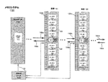
図1は、メモリコントローラ110と、第1のメモリモジュール118の形態のメモリ素子の第1のセットと、第2のメモリモジュール120の形態のメモリ素子の第2のセットとを利用する完全バッファ型メモリシステム100の一実施形態を示す。ポイントツーポイントシリアルリンク140a、140b、および150a、150bの形態の上流信号パスおよび下流信号パスのそれぞれは、コントローラをメモリモジュールにデイジーチェーン構成で結合する。クロックソース130は、システムクロック信号をコントローラおよびメモリモジュールに配布する。
FIG. 1 illustrates a fully buffered type utilizing a
一実施形態では、メモリコントローラ110は、完全バッファ型デュアルインラインメモリモジュール(FBDIMM)信号伝送プロトコルに従って、シリアル化された制御信号、アドレス信号および書き込みデータ信号を送信し、シリアル化された読み出しデータ信号を受信するという点で、FBDIMMとの併用に利用されるものと同様であり得る。一般に、これは、多重化された制御信号、アドレス信号、および書き込みデータ信号をコントローラから第1のメモリモジュールに下流シリアルリンク140aに沿って駆動するシリアルリンク送信器の形態の送信回路を含む。コントローラ上の受信器回路は、上流シリアルリンク150aとインタフェースして、シリアル化された読み出しデータを第1のモジュール118から受信する。コントローラは階層回路180を利用して、より完全に以下に開示するように、階層アクティビティを管理することができる。
In one embodiment, the
引き続き図1を参照すると、第1のメモリモジュール118は、集積回路(IC)の形態のバッファ素子125と、ダイナミックランダムアクセスメモリ(DRAM)ICの形態の複数の揮発性メモリ素子103a〜103hとを含む。バッファICは、コントローラ110および第2のメモリモジュール120と通信するための上流ポートおよび下流ポートの各ペアを含む。一実施形態では、バッファICは、コントローラ階層回路180を補うか、またはコントローラ階層回路180と置換され得る階層回路190を含む。バッファICは、制御/アドレスバスおよびデータバス(明確にするために、単一のバスとして示される)のそれぞれを介してDRAM素子と通信する。DRAM素子は、XDR(n)型またはDDR(n)型であってよく、一般に、非常に高速な読み書き時間および高密度を特徴とし得る。
With continued reference to FIG. 1, the first memory module 118 includes a buffer element 125 in the form of an integrated circuit (IC) and a plurality of
図1をさらに参照すると、第2のメモリモジュール120は第1のメモリモジュール118と同様であり、バッファIC126および複数のメモリ素子104a〜104hを有する。しかし、第2のモジュールのメモリ素子は、フラッシュメモリ等の不揮発性の種類のものである。フラッシュ素子は、低コスト、低電力、高密度を特徴とし、DRAMと同様の速度でデータを読み出すことが可能である。しかし、フラッシュ素子への書き込み動作には、通常、完了までに数ミリ秒かかることが多い消去時間が含まれる。さらに、フラッシュ素子は、同じ記憶ブロックへのデータ書き込みの点で限られた耐久性を有する。これに対処するために、バッファICは、より完全に以下に説明するように、不揮発性素子への書き込み動作を最適化する回路を含む。
With further reference to FIG. 1, the
一実施形態では、第1および第2のモジュール118および120は、上流シリアルリンク140および下流シリアルリンク150を介して、ポイントツーポイントデイジーチェーン様式で各バッファICを介して相互接続される。このようにして、コントローラ110および第2のモジュール120が関わる任意のトランザクションでは、データは必然的に、第1のモジュール118を通って流れる。不揮発性素子セットよりも揮発性メモリ素子セットをコントローラの近くに位置決めすることにより、第1レベル階層および第2レベル階層のそれぞれを101および102において定義することができる。
In one embodiment, the first and
上述した階層構造は、多くの方法で拡張可能である。例えば、1つまたは複数の揮発性メモリモジュールを第1レベル階層に編成し、第2レベルメモリ階層を確立する1つまたは複数の不揮発性モジュールの上流(コントローラのより近く)に位置決めすることができる。 The hierarchical structure described above can be extended in many ways. For example, one or more volatile memory modules can be organized into a first level hierarchy and positioned upstream (closer to the controller) of one or more non-volatile modules establishing a second level memory hierarchy. .
各モジュールの位置および素子の種類によって定義される階層に従ってのシステムの動作をサポートするために、揮発性メモリモジュールおよび不揮発性メモリモジュールのバッファIC125および126は、より完全に以下に説明するように、トランザクションを調整するに当たってメモリコントローラ110を支援するロジックを含む。
In order to support system operation according to a hierarchy defined by the location of each module and the type of element, the buffer ICs 125 and 126 of the volatile and non-volatile memory modules are more fully described below, as described below. It includes logic that assists the
図2Aは、一実施形態におけるHRCH回路190を有するICバッファ素子200aを示す。ICバッファ素子200aは、図1に示されるICバッファ素子126に対応し、1つまたは複数の不揮発性メモリモジュール120によって利用される。代替の実施形態では、HRCH回路190のうちの1つまたは複数の回路は、コントローラ110内に配置されてもよく、またはコントローラ110とICバッファ素子126との間に分散してもよい。ICバッファ素子200aは、メモリモジュール上に配置してもよく、ICメモリ素子もしくはダイと共に共通のパッケージ内に収容されてもよく、またはパーソナルコンピュータもしくはサーバのマザーボード、例えば、メインメモリに配置されてもよい。ICバッファ素子200aは、埋め込みメモリサブシステム、例えば、コンピュータグラフィックスカード、ビデオゲームコンソール、またはプリンタ等で見出される埋め込みメモリサブシステム内で使用されてもよい。
FIG. 2A illustrates an IC buffer element 200a having an HRCH circuit 190 in one embodiment. The IC buffer element 200a corresponds to the IC buffer element 126 shown in FIG. 1 and is used by one or more
引き続き図2Aを参照すると、制御情報、書き込みデータ、および読み出しデータを信号パス201から受信し、制御情報、書き込みデータ、および読み出しデータを、不揮発性集積回路メモリ素子(第2レベル階層に関連する)または揮発性集積回路メモリ素子(第1レベル階層に関連する)への信号パス202に出力するインタフェース210が示される。一実施形態では、信号パス201は、図1に示される信号パス140a、140bに対応し、その一方で、信号パス202は信号パス150a、150bに対応する。一実施形態では、ICバッファ素子200aに結合された集積回路メモリ素子を対象とした制御情報、書き込みデータ、および読み出しデータの多重化された組み合わせが、インタフェース210を介して受信され、インタフェース210は、例えば、制御情報を抽出することができる。例えば、メモリコマンドおよびアドレス情報を復号化し、信号パス210上の多重化情報から分離し、インタフェース210から要求・アドレス回路240に提供することができる。書き込みデータは、インタフェース210によってインタフェース220a、220bに提供することができ、集積回路メモリ素子からの読み出しデータを1つまたは複数のインタフェース220a、220bにおいて受信し、マルチプレクサ230a、230bを介してインタフェース210に提供することができる。
With continued reference to FIG. 2A, control information, write data, and read data are received from
インタフェース220a、220bは別個のインタフェースとして示されるが、組み合わせられてもよい。インタフェース220a、220bは、不揮発性メモリ素子に送信中であるか、または不揮発性メモリから受信中のデータを記憶するために使用されるトランザクションキュー221a、221bを含む。バッファ200aが不揮発性メモリ素子に適用された場合、トランザクションキューは、トランザクションを記憶し、データを単一または制限された数のメモリ素子に宛てる。このデータ編成では、すべての素子ではなく少数のみのメモリ素子に書き込むことによってトランザクションが行われるため、トランザクションによって実行される書き込み動作の数が低減する。メモリ素子に送信中およびメモリ素子から送信中のデータは、インタフェース210内のトランザクションキュー223aに転送されてから、上流シリアルインタフェースおよび下流シリアルインタフェースに送信される。同様に、信号パス201からシリアルに受信されたトランザクションは、トランザクションキュー223aに記憶され、次いで、インタフェース220a、220b内のトランザクションキュー221a、221bに転送されてから、メモリ素子に送信される。この編成では、上流リンクおよび下流リンクに接続されたシリアルインタフェース210上の単一のトランザクションが、信号パス121および122に接続された不揮発性メモリ素子のうちの1つのみまたは2つのみにマッピングされる。
一実施形態では、クロック信号および他の情報が、信号パス201上で、またはシリアルバス等の他のパスによって受信される。一実施形態では、インタフェース210は、信号を信号パス202に出力し、信号パス201上で受信するために、送信回路または送信器と、受信器回路または受信器(またはまとめて送受信器と呼ばれる)を含む。同様に、インタフェース220aおよび220bは、それぞれ信号パス121および122を介して制御情報、読み出しデータ、および書き込みデータを集積回路メモリ素子に送信し、集積回路メモリ素子から受信する。一実施形態では、インタフェース220a、220bは、信号パス121および122に信号を出力し、信号パス121および122に信号を受信する送信器および受信器を含む。実施形態では、インタフェース210、220a、および220b内の送信器および受信器は、単独または組み合わせで、信号パス121および122内の特定の信号線専用であるか、または共用される。
In one embodiment, clock signals and other information are received on
一実施形態では、インタフェース220a、220b内の送信器および受信器は、同期NAND型(Synch Nand)フラッシュまたはNOR型フラッシュ書き込み/読み出し/消去/制御信号等の標準揮発性メモリ素子信号伝送特性(またはプロトコル)を有する信号を送受信する。
In one embodiment, the transmitters and receivers in the
一実施形態では、インタフェース220a、220bは、制御情報を単方向信号パスで転送する送信器を含む一方で、書き込みデータおよび読出しデータを双方向信号パスで転送する、書き込みデータおよび読み出しデータ用の送信器および受信器を含む。一実施形態では、インタフェース220a、220b、および210内の送信器は、単独または組み合わせで、信号パス121、122、および401上に各信号を出力する出力ドライバ回路である。出力ドライバ回路は、プルアップ型、プルダウン型、および/またはプッシュプル型の出力ドライバ回路であってよい。
In one embodiment, the
一実施形態によれば、マルチプレクサ230aおよび230bは、インタフェース210とインタフェース220aおよび220bとの間で帯域幅集約動作を実行すると共に、データを適切な発信元(すなわち、信号パスのターゲットサブセット、内部データキャッシュ−キャッシュ回路292)から適切な宛先にルーティングする。一実施形態では、帯域幅集約は、複数の信号パス実施形態内の各信号パスの(より小さな)帯域幅を結合して、より小さな信号パスグループで利用される(より高い)全体帯域幅に合わせることを含む。帯域幅集約は、通常、複数の信号パスとより小さな信号パスグループとの間でスループットの多重化および多重分離を利用する。一実施形態では、ICバッファ素子200aは、インタフェース210の帯域幅と合ったインタフェース220aおよび220bの結合帯域幅を利用する。
According to one embodiment, multiplexers 230a and 230b perform bandwidth aggregation operations between
図2Aをさらに参照すると、一実施形態では、HRCH回路190は、制御回路290、マッピング回路291、キャッシュ(または記憶)回路292、耐久性回路293(1つまたは複数の記憶された書き込み閾値293aを含む)、および欠陥回路294(1つまたは複数の記憶された欠陥メモリアドレスを含む)を単独または組み合わせで含む。ICバッファ200a内に示された回路は、図4に示すように結合され得る。HRCH回路190の1つまたは複数の回路構成要素も、各種実施形態では、HRCH回路190内ではなく、コントローラ110内、特にHRCH回路180内に配置され得る。
With further reference to FIG. 2A, in one embodiment, the HRCH circuit 190 includes a
制御回路290は、HRCH回路190内の回路への制御信号の提供およびそのような回路からの制御信号の受信を担当する。一実施形態では、制御回路290は、インタフェース210から信号パス201を介して制御信号および/または値を受信することができる。制御情報は、コントローラ110、プログラマブル回路(SPD素子等)、および/または別のメモリモジュールからのコマンドの形態で提供され得る。一実施形態では、制御回路290は、プロセッサ、コントローラユニット、および/または制御ロジックである。制御回路290は、図4に示される信号パス405と同様に、信号パスによってHRCH内の他の回路に結合される。読み出しデータ、書き込みデータ、およびアドレス、ならびに制御信号は、信号パスを使用して回路間で転送され得る。一実施形態では、制御回路290は、ICバッファ素子200aも操作し、圧縮/圧縮解除エンジンを含み得る。
The
マッピング回路291は、書き込み/読み出しデータに関連するアドレスまたはメモリロケーションのリマッピングまたは再割り当てを担当する。マッピング回路291は、制御回路290(および/または耐久性回路293および欠陥回路294)からの制御信号に応答して、アドレスおよびデータを図3Aおよび図3Bに示されるようにリマッピングする。一実施形態では、マッピング回路291は、アドレス変換回路を含み得る。マッピング回路291は、キャッシュ回路292内の関連する読み出し/書き込みデータと共に記憶されたアドレスをリマッピングし得る。マッピング回路291は、データをインタフェース210からインタフェース220内の適切なトランザクションキューに宛て、インタフェース210から受信したアドレスを選択された適切な素子およびメモリアドレスに変換し、変換されたものはインタフェース220a、220bに送信される。一般に、必要とされる書き込み動作の数を低減するために、揮発性メモリシステム内で、インタフェース210からの単一のトランザクションは1つまたは少数のメモリ素子に宛てられ、インタフェース210上の連続したアドレスが、単一のメモリ素子内の連続したロケーションに宛てられる。
The
キャッシュ回路292は、コントローラまたは別のメモリモジュールからの読み出し/書き込みデータを記憶するために使用される。一実施形態では、読み出し/書き込みデータは、システム100内のメモリロケーションへの関連するアドレスと共に記憶される。読み出し/書き込みデータは、64Kバイト、128Kバイト、256Kバイト、および/または512Kバイトのブロック等の連続したワードまたはバイトのグループで記憶し集めることができる。この場合、これらブロックをグループとして転送し記憶することができる。例えば、256Kバイトの書き込みデータブロック(信号パス140aおよび140bを介してコントローラ110から受信した)をバッファ素子125bのキャッシュ回路292に記憶し、信号パス140cを介して、書き込みデータが記憶されている(または一実施形態では、前回の書き込み後に再記憶された)メモリモジュール120cに転送することができる。別の実施形態では、特定のメモリモジュールに関連付けられた集積回路メモリ素子が、キャッシュ回路292に代えて、データブロックの記憶に使用される。
The
耐久性回路293は、システム100内の特定のメモリロケーション(または複数のメモリロケーション)において行われた書き込み動作の数に基づいて、書き込み/読み取りデータをリマッピングすべきか否かを決定することを担当する。一実施形態では、耐久性回路293は、書き込み閾値を記憶し、または特定のメモリロケーションへのさらなる書き込みまたは記憶の確実性がなくなる危険性が生じる以前に、特定のメモリロケーションへの書き込み回数を制限する1つまたは複数のレジスタ等の記憶回路を含む。一実施形態では、耐久性回路293は、特定のメモリロケーションへの書き込み回数をカウントするカウンタと、カウント値を記憶されている書き込み閾値と比較する比較回路とも含む。次いで、比較回路は、比較に応答して、特定のメモリロケーションに書き込むべきではないことを示す制御信号を制御回路290に出力し得る。次いで、マッピング回路291は、新しいアドレスを、1つまたは複数のメモリモジュールに記憶されるべき書き込み/読み出しデータに割り当てることができる。耐久性回路293は、特定のメモリロケーションに他のメモリロケーションほどはまだ書き込まれていないことを示す制御信号も生成し得、したがって、マッピング回路291は、不揮発性集積回路メモリ素子に記憶された書き込み/読み出しデータの分散を可能にする。
欠陥回路294は、1つまたは複数のメモリロケーションが欠陥を有するか否か、または情報を正確に記憶し出力していないかどうか決定することを担当する。一実施形態では、欠陥回路294は、制御回路290からの制御信号に応答して、別のメモリモジュール内の1つまたは複数のメモリロケーションに書き込まれる複数のテスト値294aを記憶する。次いで、比較回路により、他のメモリモジュールに記憶されたテスト値が再びICバッファ素子200aに読み出され、記憶された複数のテスト値294aと比較される。比較回路は、比較に応答して、メモリロケーションが欠陥を有することを示す信号を出力する。次いで、書き込み/読み出しデータのさらなるリマッピングが、識別された欠陥メモリロケーションを含まないように、制御信号をマッピング回路291に出力することができる。一実施形態では、欠陥回路294は、制御回路290および/またはマッピング回路291によってアクセスされ得る欠陥メモリロケーションのアドレスを記憶する。一実施形態では、複数のテスト値294aは、コントローラ110によって提供される疑似乱数生成器により、テストパターンとして生成されるか、または別のメモリモジュールの内容を読み取ることによって得られる。
The
代替の実施形態では、欠陥回路294は、メモリロケーションからの電流/電圧を感知し、電流/電圧を表す記憶されている値と比較して、メモリロケーションが欠陥を有するか否かを決定する感知回路を含む。
In an alternative embodiment, the
各種実施形態では、HRCH回路190を含むICバッファ素子200aは、異なる動作モードで動作する。第1の動作モードでは、ICバッファ素子200aは、別のメモリモジュールおよび/またはコントローラによってアクセスされるべき読み出し/書き込みデータを記憶する。第2の動作モードでは、ICバッファ素子200aは、別のメモリモジュール内のアドレスを読み出し/書き込みデータに割り当て、データおよびアドレスを別のメモリモジュールに転送し、次いで、別のメモリモジュールは読み出し/書き込みデータを記憶する。 In various embodiments, the IC buffer element 200a including the HRCH circuit 190 operates in different operation modes. In the first mode of operation, the IC buffer element 200a stores read / write data to be accessed by another memory module and / or controller. In the second mode of operation, the IC buffer element 200a assigns an address in another memory module to read / write data, transfers the data and address to another memory module, and then the other memory module reads / writes. Store the data.
クロック回路270は、外部クロックを基準にして内部クロック信号の位相または遅延を調整するための1つまたは複数のクロックアラインメント回路を含む。クロックアラインメント回路は、クロックソース130等の既存のクロック発生器からの外部クロックを利用してもよく、または内部クロックを提供し、所定の時間関係を有する内部同期クロック信号を生成する内部クロック発生器を利用してもよい。一実施形態では、クロック回路270は、位相ロックループ回路または遅延ロックループ回路を含む。一実施形態では、クロックアラインメント回路は、転送または受信された制御情報、読み取りデータ、および/または書き込みデータに対して時間関係を有する内部クロック信号を提供する。 Clock circuit 270 includes one or more clock alignment circuits for adjusting the phase or delay of the internal clock signal relative to the external clock. The clock alignment circuit may use an external clock from an existing clock generator such as the clock source 130, or may provide an internal clock and generate an internal synchronous clock signal having a predetermined time relationship. May be used. In one embodiment, clock circuit 270 includes a phase locked loop circuit or a delay locked loop circuit. In one embodiment, the clock alignment circuit provides an internal clock signal that has a temporal relationship to the transferred or received control information, read data, and / or write data.
実施形態では、インタフェース220a、220b(ならびにインタフェース210)内の送信器は、符号化クロック情報を含む差分信号を送信し、受信器は、符号化クロック情報を含む差分信号を受信する。一実施形態では、クロック回路270は、受信器によって受信されたデータに符号化されたクロック情報を抽出する。さらに、クロック情報は、送信器によって送信されるデータにも符号化される。例えば、クロック情報は、所与のデータビット数中に発生する信号遷移数が最小になることを保証することにより、データ信号に符号化してもよい。
In an embodiment, transmitters in
シリアルインタフェース274は、シリアル情報をコントローラ110、別のICバッファ素子、または実施形態での他の構成回路から受信し/に送信するインタフェースである。シリアル情報は、ICバッファ素子200aまたはメモリモジュールの初期化値/信号を含むことができる。一実施形態では、シリアルインタフェース274は、コントローラ110によって使用されて、1つまたは複数の書き込み閾値293aおよび/またはテスト値294a等の値をHRCH回路190に記憶し、かつ/またはHRCH回路190内の値を読み出す。
The serial interface 274 is an interface for receiving / transmitting serial information from the
図2Bは、図2Aに示されるバッファIC200aと同様であるが、揮発性メモリモジュール118(図1)と併用されるバッファIC200bを示す。2つのバッファIC内の回路の大半は同様であり、簡潔にするために、再び説明しない。しかし、耐久性回路293aおよび欠陥回路294a(図2A)の省略等の回路に対する特定の変更が利用され得る。さらに、トランザクションキューおよびマッピング回路は、不揮発性モジュールバッファIC200aによって利用されるデータマッピングと異なるようにデータマッピングを処理する。
FIG. 2B shows a buffer IC 200b similar to the buffer IC 200a shown in FIG. 2A, but used in conjunction with the volatile memory module 118 (FIG. 1). Most of the circuits in the two buffer ICs are similar and will not be described again for the sake of brevity. However, certain changes to the circuit such as omission of the
マッピング回路291は、一般に、データをインタフェース220に宛てると共に、インタフェース220からデータをすべての素子に並列に宛てるように構成され、同様のアドレスが、素子のうちのすべてまたは大半に同時に送信され、多くのデイス(deice)が単一のトランザクションによって選択される。
The
インタフェース220a、220bは別個のインタフェースとして示されるが、組み合わせてもよい。インタフェース220a、220bは、揮発性メモリ素子に送信中または揮発性メモリ素子から受信中のデータの記憶に使用されるトランザクションキュー222a、222bを含む。バッファ200bがDRAMのような揮発性メモリ素子に適用される場合、トランザクションキューは、多くの素子に宛てられ、多くの素子に分散してトランザクションを記憶する。この場合、素子の結合帯域幅は並列にアクセスされて、トランザクションの帯域幅が最大化される。メモリ素子に送信中のデータおよびメモリ素子から送信中のデータは、インタフェース210内のトランザクションキュー223bに転送されてから、上流シリアルインタフェースおよび下流シリアルインタフェースに送信される。同様に、信号パス201からシリアルに受信されたトランザクションは、トランザクションキュー223bに記憶され、次いで、222a、222bにおけるトランザクションキューに転送されてから、メモリ素子に送信される。この編成では、インタフェース210内の上流リンクまたは下流リンク上の単一のトランザクションは、メモリから読み出されるとき、または書き込まれるときに、複数のメモリ素子にアクセスする。
上述したように、フラッシュメモリ素子およびDRAMメモリ素子は、多くの異なる特性を有する。さらなる違いには、データ書き込み動作が素子内でどのように実行されるかが含まれる。 As described above, flash memory devices and DRAM memory devices have many different characteristics. Further differences include how data write operations are performed within the device.
図3Aは、DRAMベースのFBDIMMモジュール318とフラッシュベースのFBDIMMモジュール320との間の相対データマッピングの一例を示す。DRAMベースのFBDIMMメモリモジュール内では、モジュール上のDRAM素子303a〜303hがデータバス幅を定義する。そして、この幅は、各クロックエッジにおいてすべてのDRAMに同時に書き込むことが可能なビット数を示す。同時書き込みのそれぞれは、図3Aの揮発性素子303a〜303h内の影付きエリアによって象徴的に示されるように、各DRAM内の同じアドレスにおいて実行される。したがって、各クロックサイクル中に、データの部分が各DRAMに書き込まれる。バッファIC325は、シリアル化解除回路(図示せず)を提供して、上流シリアルリンク340aまたは下流シリアルリンク350bから受信されたシリアルストリームを並列データストリームに変換し、並列データパス328a〜328hに沿って個々のDRAM素子に送信する。
FIG. 3A shows an example of relative data mapping between a DRAM-based
並列同時書き込み方式は、DRAMベースのメモリモジュールではうまく機能する一方で、種々の理由により、フラッシュベースのモジュール用のこのような方法は非現実的である。フラッシュ素子は、多くの場合、ブロックと呼ばれるメモリ単位で消去および再プログラムを行う。さらに、データをフラッシュ素子に記憶または書き込むには、ブロックを空にするか、または消去しなければならない。その結果、大半の場合、消去動作が書き込み動作の前に行われる。さらに、上述したように、フラッシュ素子は、通常、制限された書き込み耐久性を有する。 While the parallel simultaneous write scheme works well with DRAM based memory modules, for various reasons such a method for flash based modules is impractical. In many cases, flash devices are erased and reprogrammed in memory units called blocks. Further, to store or write data to the flash device, the block must be emptied or erased. As a result, in most cases, the erase operation is performed before the write operation. Furthermore, as described above, flash devices typically have limited write endurance.
図3Aをさらに参照すると、フラッシュベースのFBDIMMモジュール320は、最小数の素子を利用して、1つまたは複数の指定ブロック360(影付きブロックとして示される)内にデータを記憶するように、下流シリアルリンク340bから受信したシリアルデータをリマッピングするバッファIC326を含む。これにより、書き込み動作がブロック当たりの利用可能ストレージ利用率を最大化し、すべての素子の耐久性に影響する書き込み動作の数を最小化することが保証される。このマッピングは、2つのモジュール間で上流パスに沿って逆方向にも作用することができる。このような状況では、所与のブロックからのデータは、示されるマッピングと同様に、複数のDRAMにリマッピングされる。
With further reference to FIG. 3A, the flash-based
図3Bは、第1の階層アドレス空間363と第2の階層アドレス空間364との間でのアドレスマッピング362を示す。一実施形態では、第1のアドレス空間363は、階層101(揮発性集積回路メモリ素子を有する)内のアドレス空間(またはアドレス指定可能なメモリロケーションの量)に対応し、階層アドレス空間364は、階層102(不揮発性ICを有する)内のアドレス空間に対応する。階層アドレス空間363は、少なくとも、アドレス指定可能なメモリロケーション366a〜366nを含み、階層アドレス空間364は、少なくとも、アドレス指定可能なメモリロケーション368a〜368tを含む。一実施形態では、階層アドレス空間364は、階層アドレス空間363よりもかなり大きい。本明細書において説明したように、回路および/または実行可能命令は、データを階層アドレス空間363または階層アドレス空間364にマッピングまたは割り当てる。一実施形態では、関連するデータは、一時には、階層アドレス空間363または364のうちの一方内のアドレスが割り当てられ、次いで、前に割り当てられていた階層アドレス空間内の異なるメモリロケーションまたは異なる階層アドレス空間内の異なるメモリロケーションにおける異なるアドレスがリマッピングまたは割り当てられた読み出しデータおよび/または書き込みデータであり得る。一実施形態では、図3Bに示されたメモリロケーションは、連続したメモリロケーションのブロックまたはグループに対応する。
FIG. 3B shows
例えば、メモリロケーション364aに記憶された、または記憶されるべきデータには、メモリロケーション363bへのアドレスがマッピングまたは割り当てられ、メモリロケーション363bに記憶される。同様に、メモリロケーション363nに記憶された、または記憶されるべきデータには、メモリロケーション364tへのアドレスがマッピングされ、メモリロケーション364tに記憶される。 For example, data stored or to be stored in memory location 364a is mapped or assigned an address to memory location 363b and stored in memory location 363b. Similarly, data stored in or to be stored in memory location 363n is mapped to an address to memory location 364t and stored in memory location 364t.
メモリロケーション364eが割り当てられたデータに、メモリロケーション364sを再割り当てし、階層アドレス空間364内のメモリロケーション364sに記憶してもよい。階層アドレス空間364内のデータの再割り当ておよび記憶は、所定数の書き込み動作が特定のメモリロケーションにおいて発生した場合、かつ/または特定のメモリロケーションが欠陥を有するか、または信頼性が低いと判断された場合に行うことができる。 The memory location 364s may be reassigned to the data to which the memory location 364e has been assigned and stored in the memory location 364s in the hierarchical address space 364. The reassignment and storage of data in the hierarchical address space 364 is determined when a predetermined number of write operations occur at a particular memory location and / or the particular memory location is defective or unreliable. Can be done.
図4は、HRCH回路180を有する、図1に示されるコントローラ110を示す。HRCH回路180は、図2Aおよび図2Bに示されるHRCH回路190と同様に動作する。コントローラ110は、信号パス140a上で制御情報および読み出し/書き込みデータを転送する、インタフェース310と同様のインタフェース401も含む。コントローラ110は、制御データおよび読み出し/書き込みデータの同期および転送に使用される、クロック回路370と同様のクロック回路403も含む。シリアルインタフェース402は、ICバッファ素子125a、125b、126a、および126b内のシリアルインタフェース374と共に使用されて、コントローラ110とICバッファ素子125a、125b、126a、および126bとの間にシリアル情報を提供する。
FIG. 4 shows the
一実施形態では、コントローラ110またはICバッファ素子300の制御回路390は、システム100内の階層の数および種類を示す情報をSPD素子等の記憶回路から読み出す。次いで、制御回路390は、SPD素子から読み出された情報に応答して、適切な制御信号を生成することができる。
In one embodiment, the
動作に際して、上述したシステムは、モジュールの位置(例えば、上流か下流か)および素子の種類(例えば、揮発性か不揮発性か)に基づいて階層を確立することができる。上流パスおよび下流パスを含むFBDIMMのようなインフラストラクチャに結合された場合、このような構造は、準拠違反の問題を回避しながら、揮発性メモリおよび不揮発性メモリの恩恵を利用する。 In operation, the system described above can establish a hierarchy based on module location (eg, upstream or downstream) and device type (eg, volatile or non-volatile). When coupled to an infrastructure such as an FBDIMM that includes upstream and downstream paths, such a structure takes advantage of volatile and non-volatile memory while avoiding compliance violation problems.
図5A〜図5Dは、図1に示されるシステム100の動作方法500、510、520、および530を示す。上述したデイジーチェーン接続されたポイントツーポイントリンク構造を利用することにより、後述する方法の多くは、同時に実行される複数の動作を含む。さらに、実施形態では、図5A〜図5Dに示される論理ブロックは、単独または組み合わせでのハードウェア(例えば、回路)、ソフトウェア(実行可能な命令)、またはユーザの動作を表す。例えば、他の回路を有する、図1に示されるHRCH回路は、単独または組み合わせで、動作を実行することができる。示されていない他の論理ブロックを各種実施形態において含んでもよい。同様に、示されている論理ブロックは、各種実施形態において除外されてもよい。方法500、510、520、および530について逐次論理ブロックで説明するが、方法の論理ブロックによって表される動作は、非常に素早く完了されるか、または略瞬時に完了され、同時に実行し得る。
5A-5D illustrate methods of
図5Aに示される方法500は、書き込みデータのバッファリングを含み、501において、書き込みデータをメモリコントローラ110から1つまたは複数のメモリモジュールの第1の階層101に転送することによって開始される。502において、書き込みデータは第1の階層内で蓄積もされ、所定数の連続ビット値または書き込みデータブロックに集めることができる。次いで、503において、第1の階層内に蓄積された書き込みデータを第1の階層のモジュールから第2の階層102の1つまたは複数のメモリモジュールに転送することができる。次いで、504において、第1の階層に記憶された書き込みデータを退避させることができる。方法500では、第1の階層は、第2の階層の書き込みキャッシュとして機能する。第2の階層モジュール内の不揮発性メモリ素子に関連する書き込み待ち時間は約数ミリ秒であり得るため、これは重要である。データが第1の階層から第2の階層に転送されている間に、書き込みデータを第1の階層内にキャッシュすることにより、コントローラは、第2の階層モジュールを待つ必要なく、他の動作を同時に実行することができる。
The
図5Bは、第1の階層101が(コントローラ100に対して)第2の階層102の読み出しデータの読み出しキャッシュとして機能する、読み出しデータをキャッシュする方法510を示す。方法510は、511および512において、読み出しデータを所定数の連続ビット値または読み出しデータブロックに集め、次いで、読み出しデータを第2の階層から第1の階層に転送することによって開始される。第1の階層は、513において、読み出しデータブロックが第2の階層から第1の階層に転送されている間、コントローラと同時に書き込み動作および読み出し動作を同時に実行することができる。本明細書において説明する階層システムによって提供される別の有益な方法は、書き込みデータの併合を含む。場合によっては、いくつかの所望のデータの部分が第2の階層102内のモジュールにすでに記憶されている間、別の部分を第1の階層101内のモジュールに記憶することができる。第2の階層(不揮発性素子を有する)内のブロックへのいかなる書き込みも、まず、ブロック全体の内容を消去することを含む。したがって、ブロックの元の内容の消失を回避するために、図5Cに示される「読み出し−変更−書き込み」の形態の一連のステップを利用することができる。
FIG. 5B shows a
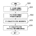
図5Cをさらに参照すると、書き込みデータを併合する方法520は、まず、521において、所望のデータ「データA」をモジュールの第1の階層101内の揮発性メモリ素子から読み出すことを含む。データは、揮発性メモリモジュールバッファIC125または不揮発性メモリモジュールバッファIC126のうちの一方に一時的に記憶することができる。次いで、ステップ522に示されるように、不揮発性素子からの所望のデータブロック「ブロックB」が、第2の階層102内のメモリモジュールから読み出され、データAを記憶している同じバッファIC内に一時的に記憶される。次いで、ステップ523において、データAおよびブロックBは、バッファ回路によって一緒に併合される。次いで、524において、併合データ「データA」および「ブロックB」は、単一のデータブロック「ブロックC」として再び第2の階層に書き込まれる。
With further reference to FIG. 5C, the
図5Dは、531において、書き込みデータAを第1の階層101に転送することによって開始される方法530を示し、書き込みデータAは、書き込みデータブロックに記憶またはキャッシュされてから、第2の階層102に書き込まれる。532において、第1の階層内にキャッシュされた書き込みデータAのブロックがアクセスされる。次いで、533において、キャッシュされた書き込みデータAのブロックは、第1の階層から第2の階層に転送され、第2の階層に記憶され、その間、第1の階層内のデータBが、読み出し動作等を通して同時にアクセスされる。図5Dは、同時動作を含む方法の一実施形態を示すが、コントローラならびにバッファ素子110、125、および126を相互接続するデイジーチェーン接続された上流ポイントツーポイントリンク140a〜140nおよび下流ポイントツーポイントリンク150a〜150nにより、同時動作の各種実施形態が可能である。例えば、コントローラ110と第1の階層のメモリ素子との間の読み出し動作および/または書き込み動作は、第1レベルのメモリ階層と第2レベルのメモリ階層との間で実行される書き込み動作および/または読み取り動作と同時に実行することができる。
FIG. 5D illustrates a
図1に示された実施形態に戻ると、メモリモジュール120a〜120dは、信号パス140a〜140dに結合するための、ピンおよび/またはボール等の複数の導通接点を有するインタフェース123a〜123dを有する基板を含む。一実施形態では、複数の接点、はんだボール、またはピンがインタフェースに含まれ、インタフェースとメモリモジュール基板との間に電気接続を提供する。一実施形態では、インタフェースは、コネクタまたはプリント回路基板等の基板から着脱可能であり得る。一実施形態では、コントローラ110、集積回路メモリ素子103a〜103pおよび104a〜104p、ならびにICバッファ素子125a、125b、126a、および126bは、集積モノリシック回路に別個に収容され、かつ/または複数のパッケージ内で結合される(例えば、単一のパッケージ内のメモリ素子およびバッファ素子)。パッケージは、1つまたは複数の基板上に配置することができる。
Returning to the embodiment shown in FIG. 1, memory modules 120a-120d have substrates 123a-123d having a plurality of conductive contacts, such as pins and / or balls, for coupling to signal
一実施形態では、1つまたは複数の信号パス140a〜140dは、1つまたは複数の信号線を示すポイントツーポイントリンクであり、各信号線は、2つのみの送受信器接続ポイントを有し、各送受信器接続ポイントは、送信器回路、受信器回路、または送受信器回路に結合される。例えば、ポイントツーポイントリンクは、一端に、またはその近傍に結合された送信器と、他端に、またはその近傍に結合された受信器とを含むことができる。
In one embodiment, one or
実施形態では、1つまたは複数の信号パス140a〜140dは、異なる種類のバスまたはポイントツーポイントリンク構造を含むことができる。実施形態では、信号パスは、異なる種類の信号伝送およびクロッキング種別構造を有することもできる。異なるリンク構造を有する実施形態は、同時双方向リンク、時間多重化双方向リンク、および複数の単方向リンクを含む。電圧モード信号伝送または電流モード信号伝送は、これらリンク構造またはバス構造の任意のものに利用することができる。一実施形態では、信号パス140a〜140dは、SMBus等のシリアルデータバスを含む。シリアルデータは、シリアルインタフェース474を介してコントローラ110を1つまたは複数のICバッファ素子125a、125b、126a、および126bに結合することができる。
In an embodiment, the one or
一実施形態では、1つまたは複数のメモリモジュール120a〜120dは、標準DIMMフォームファクタを有するデュアルラインメモリモジュール(「DIMM」)である。一実施形態では、メモリモジュールは、「システムインパッケージ」(「SIP」)のように、単一の単体パッケージに含むことができる。一種のSIP実施形態では、メモリモジュールは、互いの上に積み重ねられ、導電性相互接続を介して結合された一続きの集積回路ダイ(すなわち、メモリ素子およびバッファ素子)を含むことができる。はんだボールまたは配線リードは、メモリモジュールをプリント回路ボード基板に固定して取り付けることができるように、コネクタインタフェースとして利用することができる。コネクタインタフェースは、例えば、メモリモジュールがシステムの残りの部分から着脱可能なように、オス型部およびメス型部を含む物理的に分離可能な種類のものであってもよい。別のSIP実施形態は、二次元構成で共通の基板平面上に配置され、単一のパッケージ筐体内に置かれたいくつかのメモリ素子およびバッファ素子を含むことができる。 In one embodiment, the one or more memory modules 120a-120d are dual line memory modules ("DIMM") having a standard DIMM form factor. In one embodiment, the memory modules may be included in a single unitary package, such as a “system in package” (“SIP”). In one type of SIP embodiment, a memory module can include a series of integrated circuit dies (ie, memory elements and buffer elements) stacked on top of each other and coupled via conductive interconnects. The solder balls or wiring leads can be used as a connector interface so that the memory module can be fixedly attached to the printed circuit board substrate. The connector interface may be of a physically separable type that includes, for example, a male part and a female part so that the memory module is removable from the rest of the system. Another SIP embodiment can include several memory and buffer elements placed on a common substrate plane in a two-dimensional configuration and placed in a single package housing.
図1に示される実施形態では、集積回路メモリ素子103a〜103pおよび104a〜104pは、異なる種類の集積回路メモリ素子を含む。例えば、集積回路メモリ素子103a〜103pは、揮発性集積回路メモリ素子であってもよく、その一方で、集積回路メモリ素子104a〜104pは不揮発性集積回路メモリ素子であってもよい。一実施形態では、揮発性集積回路メモリ素子は、電力が素子から除去されると、記憶された情報が失われる複数のメモリセルを含む。これとは対照的に、一実施形態では、不揮発性集積回路メモリ素子は、電力が素子から除去されても情報が保持される複数のメモリセルを含む。
In the embodiment shown in FIG. 1, integrated
揮発性メモリ素子の種類としては、ダイナミックランダムアクセスメモリ(「DRAM」)、分子電荷ベース(molecular charge-based)(ZettaCore)DRAM、浮遊ボディ(floating-body)DRAM、およびスタティックランダムアクセスメモリ(「SRAM」)が挙げられるが、これらに限定されない。DRAMの特定の種類としては、ダブルデータレートSDRAM(「DDR」)または後世代のSDRAM(例えば、「DDR2」または「DDR3」)、ならびにXDR(商標)DRAMまたはDIRECT RAMBUS(登録商標)DRAM(「DRDRAM」)が挙げられる。 Volatile memory device types include dynamic random access memory ("DRAM"), molecular charge-based (ZettaCore) DRAM, floating-body DRAM, and static random access memory ("SRAM"). )), But is not limited thereto. Specific types of DRAM include double data rate SDRAM (“DDR”) or later generation SDRAM (eg, “DDR2” or “DDR3”), as well as XDR ™ DRAM or DIRECT RAMBUS ™ DRAM (“ DRDRAM ").
不揮発性メモリ素子の種類としては、電気的消去可能プログラム読み取り専用メモリ(「EEPROM」)、フラッシュ(NAND型フラッシュおよびNOR型フラッシュを含む)、ONO型フラッシュ、磁気抵抗RAMまたは磁気RAM(「MRAM」)、強誘電性RAM(「FRAM」)、ホログラフィック媒体、オボニック/位相変化、ナノ結晶、ナノチューブRAM(Nanotube RAM)(NRAM−Nantero)、MEMS走査プローブシステム、MEMSカンチレバースイッチ、ポリマー、分子、ナノ浮遊ゲート、および単電子が挙げられるが、これらに限定されない。 Non-volatile memory device types include electrically erasable program read only memory (“EEPROM”), flash (including NAND flash and NOR flash), ONO flash, magnetoresistive RAM or magnetic RAM (“MRAM”). ), Ferroelectric RAM (“FRAM”), holographic media, ovonic / phase change, nanocrystal, Nanotube RAM (NRAM-Nantero), MEMS scanning probe system, MEMS cantilever switch, polymer, molecule, nano Examples include, but are not limited to, floating gates and single electrons.
不揮発性メモリ素子のいくつかの種類の一特性は、一度にバイトまたはワードをランダムアクセス様式で読み出し、またはプログラム/書き込むことができるが、一度にブロックを消去しなければならないことである。新しく消去されたブロックから始まり、そのブロック内の任意のバイトをプログラムすることができる。しかし、バイトがプログラムされると、通常、ブロック全体が消去されるまで、再び変更することができない。例えば、NOR型フラッシュメモリ素子は、ランダムアクセスでの読み出し動作およびプログラム動作を提供することができるが、通常、ランダムアクセスでの書き換え動作または消去動作を提供することができない。 One characteristic of some types of non-volatile memory devices is that bytes or words can be read or programmed / written in a random access manner at a time, but the block must be erased at a time. Starting from a newly erased block, any byte in that block can be programmed. However, once a byte is programmed, it usually cannot be changed again until the entire block is erased. For example, a NOR flash memory device can provide a read operation and a program operation with random access, but normally cannot provide a rewrite operation or an erase operation with random access.
集積回路メモリ素子は、複数の感知増幅器と共に行・デコーダ回路(row and decoder circuit)によって(ワードおよびビットラインを介して)二次元メモリセルの1つまたは複数のストレージアレイ(またはバンク)を含むことができる。様々な量の電圧または電流を、ストレージアレイ内の1つまたは複数のメモリセルに付与して、論理値(例えば、論理1または論理0)に対応する電圧値を記憶したメモリセルのプログラム(書き込み)、読み出し、および/または消去を行うことができる。
An integrated circuit memory device includes one or more storage arrays (or banks) of two-dimensional memory cells (via words and bit lines) by a row and decoder circuit with a plurality of sense amplifiers. Can do. Various amounts of voltage or current are applied to one or more memory cells in the storage array to program (write) a memory cell that stores a voltage value corresponding to a logic value (eg,
図1に示される実施形態では、コントローラ110はマスタ装置であり、他のインタフェースまたは機能、例えば、チップセットのノースブリッジチップを含む集積回路素子であることができる。マスタ装置は、マイクロプロセッサまたはグラフィックスプロセッサユニット(「GPU」)またはビジュアルプロセッサユニット(「VPU」)上に集積することができる。マスタ装置は、フィールドプログラマブルゲートアレイ(「FPGA」)として実施することができる。システム100は、サーバ(例えば、ブレードサーバ)、パーソナルコンピュータ、グラフィックスカード、セットトップボックス、ケーブルモデム、携帯電話、ゲームコンソール、デジタルテレビジョンセット(例えば、高精細テレビジョン)(「HDTV」)、ファックス機、ケーブルモデム、デジタル多用途ディスク(「DVD」)プレーヤ、またはネットワークルータ等の様々なシステムまたはサブシステムに含むことができる。
In the embodiment shown in FIG. 1, the
図1に示される実施形態では、システム100は、キーワードの入力に応答して、インターネット上に記憶されたウェブサイト(またはページ)へのハイパーリンク、イメージ、および/または動画を含む検索結果を提供する検索エンジンとして実行または機能する際に使用されるサーバに使用することができる。検索エンジン実施形態では、検索頻度の高い情報(例えば、最近の検索結果)は階層101に記憶することができ、その一方で、検索頻度が低い情報(例えば、インデックス)は階層102に記憶することができる。
In the embodiment shown in FIG. 1,
本明細書において説明した信号は、導電体によってコントローラ/メモリモジュール/素子/回路間および内で送信または受信し、制限なしで、電気信号の電圧レベルまたは電流レベルを変調することを含む任意の数の信号伝送技法を使用して生成することができる。信号は、任意の種類の制御情報およびタイミング情報(例えば、コマンド、アドレス値、クロック信号、および構成情報)ならびにデータを表すことができる。一実施形態では、制御情報、アドレス情報、またはデータ情報は、特定の信号線上で特定のビットウィンドウにおいてアサートされる1つまたは複数の信号を表す要求パケット内に含まれる。一実施形態では、要求パケットは、コントローラから1つまたは複数のメモリモジュールに提供されると共に、メモリモジュール間で提供される。 Any number of signals described herein may be transmitted or received between and within a controller / memory module / element / circuit via a conductor, and without limitation, modulating the voltage level or current level of an electrical signal. Can be generated using any of the following signal transmission techniques. Signals can represent any type of control and timing information (eg, commands, address values, clock signals, and configuration information) and data. In one embodiment, control information, address information, or data information is included in a request packet that represents one or more signals that are asserted in a particular bit window on a particular signal line. In one embodiment, the request packet is provided from the controller to one or more memory modules and between the memory modules.
実施形態では、信号パスは、相互接続、導電要素、接点、ピン、半導体基板内の領域、配線、金属トレース/信号線、または光電導体等の信号を単独でまたは組み合わせて転送する媒体である。一実施形態では、図に示された単一の信号パスを複数の信号パスで置き換えてもよく、図に示された複数の信号パスを単一の信号パスで置き換えてもよい。実施形態では、信号パスは、バスおよび/またはポイントツーポイント接続を含むことができる。一実施形態では、信号パスは、制御信号線およびデータ信号線を含む。代替の実施形態では、信号パスは、データ信号線のみまたは制御信号線のみを含む。さらに他の実施形態では、信号パスは、単方向(一方向に移動する信号)または双方向(2方向に移動する信号)または単方向信号線および双方向信号線の両方の組み合わせである。 In an embodiment, a signal path is a medium that transfers signals alone or in combination, such as interconnects, conductive elements, contacts, pins, regions in a semiconductor substrate, wiring, metal traces / signal lines, or photoconductors. In one embodiment, a single signal path shown in the figure may be replaced with a plurality of signal paths, and a plurality of signal paths shown in the figure may be replaced with a single signal path. In an embodiment, the signal path may include a bus and / or point-to-point connection. In one embodiment, the signal path includes a control signal line and a data signal line. In an alternative embodiment, the signal path includes only data signal lines or only control signal lines. In still other embodiments, the signal path is unidirectional (a signal moving in one direction) or bidirectional (a signal moving in two directions) or a combination of both unidirectional signal lines and bidirectional signal lines.
本明細書において開示された各種回路は、コンピュータ支援設計ツールを使用して記述され、挙動、レジスタ転送、論理構成要素、トランジスタ、レイアウトジオメトリ、および/または他の特性に関して各種コンピュータ可読媒体に具現されるデータおよび/または命令として表現(または表す)ことができることに留意されたい。このような回路表現を実装することができるファイルおよび他のオブジェクトのフォーマットとしては、C、Verilog、およびHLDL等の挙動言語(behavioral language)をサポートするフォーマット、RTLのようなレジスタレベル記述言語をサポートするフォーマット、GDSII、GDSIII、GDSIV、CIF、MEBES等のジオメトリ記述言語をサポートするフォーマット、および任意の他の適したフォーマットおよび言語が挙げられるが、これらに限定されない。このようなフォーマットされたデータおよび/または命令を具現することができるコンピュータ可読媒体としては、各種形態(例えば、光学記憶媒体、磁気記憶媒体、または半導体記憶媒体)の不揮発性記憶媒体、ならびに無線、光、有線の信号伝送媒体またはこれらの任意の組み合わせを通してのこのようなフォーマットデータおよび/または命令の転送に使用することができる搬送波が挙げられるが、これらに限定されない。搬送波によるこのようなフォーマットデータおよび/または命令の転送の例としては、1つまたは複数のデータ転送プロトコル(例えば、HTTP、FTP、SMTP等)を介してのインターネットおよび/または他のコンピュータネットワークを経由しての転送(アップロード、ダウンロード、電子メールなど)が挙げられるが、これに限定されない。1つまたは複数のコンピュータ可読媒体を介してコンピュータシステム内で受信された場合、このようなデータおよび/または上述した回路の命令ベースの表現は、ネットリスト生成プログラム、プレースアンドルート(place and route)プログラム等を限定なしで含む1つまたは複数の他のコンピュータプログラムの実行と併せて、コンピュータシステム内の処理エンティティ(例えば、1つまたは複数のプロセッサ)によって処理して、このような回路の物理的な現れの表現またはイメージを生成することができる。その後、このような表現またはイメージは、例えば、素子組み立てプロセス内で回路の各種構成要素の形成に使用される1つまたは複数のマスクの生成を可能にすることにより、素子の組み立てに使用することができる。 The various circuits disclosed herein are described using computer-aided design tools and embodied in various computer-readable media in terms of behavior, register transfer, logic components, transistors, layout geometry, and / or other characteristics. Note that data can be expressed (or represented) as data and / or instructions. Formats of files and other objects that can implement such circuit representations include formats that support behavioral languages such as C, Verilog, and HLDL, and register level description languages such as RTL. Formats that support geometry description languages such as GDSII, GDSIII, GDSIV, CIF, MEBES, and any other suitable formats and languages. Computer-readable media that can embody such formatted data and / or instructions include non-volatile storage media in various forms (eg, optical storage media, magnetic storage media, or semiconductor storage media), and wireless, Examples include, but are not limited to, carrier waves that can be used to transfer such formatted data and / or instructions through optical, wired signal transmission media, or any combination thereof. Examples of the transfer of such formatted data and / or instructions by carrier wave are via the Internet and / or other computer networks via one or more data transfer protocols (eg, HTTP, FTP, SMTP, etc.) Transfer (upload, download, e-mail, etc.), but is not limited to this. When received in a computer system via one or more computer-readable media, such data and / or instruction-based representations of the circuits described above may be converted into a netlist generator, place and route. The physical nature of such circuitry, processed by a processing entity (eg, one or more processors) in a computer system in conjunction with execution of one or more other computer programs, including without limitation programs, etc. Representation or image can be generated. Such representations or images can then be used for device assembly, for example, by allowing generation of one or more masks used to form various components of the circuit within the device assembly process. Can do.
本明細書において説明した回路の機能は、部分的にまたは完全に、例えば、システム100内に記憶され実行可能なコンピュータ/プロセッサ実行可能命令(またはソフトウェア)で置き換えることも可能である。
The functionality of the circuits described herein may be partially or completely replaced with, for example, computer / processor executable instructions (or software) stored and executable within
好ましい実施形態の上記説明は、例示および説明のために提供された。網羅的であることや、実施形態を開示された厳密な形態に限定することは意図されない。変更および変形が当業者には明らかになるであろう。実施形態は、本発明の原理およびその実際の適用を最良に説明し、それにより、当業者が、意図される特定の用途に適した各種変更と共に各種実施形態に関して本発明を理解できるように、選択され説明された。本発明の範囲は以下の特許請求の範囲およびその等価物によって規定されることが意図される。 The above description of preferred embodiments has been provided for the purposes of illustration and description. It is not intended to be exhaustive or to limit the embodiments to the precise forms disclosed. Modifications and variations will be apparent to those skilled in the art. The embodiments best illustrate the principles of the invention and its practical application, so that those skilled in the art can understand the invention with respect to various embodiments, with various modifications suitable for the particular intended use. Selected and explained. It is intended that the scope of the invention be defined by the following claims and their equivalents.
Claims (22)
第1のメモリ階層を定義する複数の揮発性メモリ素子の第1のセットであって、第1のメモリモジュール上に配置され、当該第1のメモリモジュールは前記メモリコントローラに結合される、第1のセットと、
第2のメモリ階層を定義する1以上の不揮発性メモリ素子の第2のセットであって、第2のメモリモジュール上に配置され、当該第2のメモリモジュールは前記第1のメモリモジュールに結合される、第2のセットと
を備え、
前記第1のメモリ階層は、前記メモリコントローラからメモリトランザクションを受け取り、
データが、前記第1のメモリ階層から前記第2のメモリ階層へ、選択的に書き込まれ、
前記第2のメモリモジュールは、当該第2のメモリモジュール上に存在しない下流にあるメモリ素子のセットと結合する集積回路バッファ素子であって、特定のメモリロケーションへの書き込み回数をカウントし、書き込み回数が閾値を超えている場合に、書込み位置をリマップする集積回路バッファ素子を含む、
メモリシステム。 A memory system having a memory controller,
A first set of a plurality of volatile memory elements defining a first memory hierarchy, disposed on a first memory module, the first memory module being coupled to the memory controller; And a set of
A second set of one or more non-volatile memory elements defining a second memory hierarchy, disposed on a second memory module, the second memory module being coupled to the first memory module; And a second set,
The first memory hierarchy receives a memory transaction from the memory controller;
Data is selectively written from the first memory hierarchy to the second memory hierarchy ;
The second memory module is an integrated circuit buffer element that couples to a set of downstream memory elements that are not present on the second memory module, and counts the number of writes to a particular memory location, Includes an integrated circuit buffer element that remaps the write position when the threshold is exceeded.
Memory system.
前記メモリコントローラから受信した前記トランザクションは、キャッシュされた前記データに対するランダムアクセス書き込みトランザクションを含み、
前記トランザクションは、前記第1のメモリ階層から前記第2のメモリ階層へ選択的に送信され、前記第1のメモリ階層にキャッシュされた前記データの、ブロックをベースとした周期的な書き込みトランザクションを含み、前記キャッシュされたデータを前記1以上の不揮発性メモリ素子に記憶させる、請求項1記載のメモリシステム。 The first memory hierarchy caches data for storage in the second memory hierarchy;
The transaction received from the memory controller includes a random access write transaction for the cached data;
The transaction includes a block-based periodic write transaction of the data selectively transmitted from the first memory hierarchy to the second memory hierarchy and cached in the first memory hierarchy. The memory system of claim 1, wherein the cached data is stored in the one or more non-volatile memory elements.
前記メモリモジュール上に配置されて、第1のメモリ階層の少なくとも一部を構成する揮発性メモリ素子の第1のセットと、
前記メモリモジュールから前記下流セットに書き込みコマンドを選択的に開始して、前記不揮発性メモリ素子の第1のセットに亘って記憶されたデータ幅を示すデータを、データブロックとして前記下流セットの一部を構成する不揮発性メモリ素子の少なくとも1つに書き込む集積回路バッファであって、特定のメモリロケーションへの書き込み回数をカウントし、書き込み回数が閾値を超えている場合に、書込み位置をリマップする集積回路バッファ素子を含み、
前記メモリモジュールが、前記メモリコントローラ及び前記メモリ素子の前記下流セットに接続するようになされており、
前記メモリモジュールは、前記メモリコントローラから複数のメモリトランザクションを受け取り、前記複数のメモリ動作を示す書き込みデータを蓄積し、前記メモリモジュールから前記下流セットに、蓄積された前記書き込みデータを含むデータブロックを選択的に転送するためのものである、メモリモジュール。 A memory module for use in a memory system having a memory controller and a downstream set of at least one non-volatile memory device comprising:
A first set of volatile memory elements disposed on the memory module and constituting at least part of a first memory hierarchy ;
A write command is selectively initiated from the memory module to the downstream set, and data indicative of the data width stored across the first set of non-volatile memory elements is taken as a data block as part of the downstream set Integrated circuit buffer for writing to at least one of the non-volatile memory elements constituting the memory, wherein the number of times of writing to a specific memory location is counted, and if the number of times of writing exceeds a threshold, the integrated circuit is remapped Including a buffer element ;
Said memory module, said being adapted to connect to a downstream set of the memory controller and the memory device,
The memory module receives a plurality of memory transactions from the memory controller, accumulates write data indicating the plurality of memory operations, and selects a data block including the accumulated write data from the memory module to the downstream set. Memory module that is intended for transfer.
前記メモリモジュールは、同様のアドレスにおける、前記DRAM素子の並列セットに、書き込みデータを蓄積し、
前記メモリモジュールは、前記並列セットから、前記下流セットにおいて記憶されるデータ値のブロックに、前記書き込みデータをリマッピングすることにより、前記書き込みデータを、前記揮発性メモリ素子の第1のセットから前記下流セットに選択的に転送する、請求項9記載のメモリモジュール。 The first set of volatile memory elements includes DRAM elements, the DRAM elements organize a parallel set indicating a common address range;
The memory module stores write data in a parallel set of DRAM devices at similar addresses,
The memory module re-writes the write data from the first set of volatile memory elements by re-mapping the write data from the parallel set to a block of data values stored in the downstream set. The memory module according to claim 9 , wherein the memory module is selectively transferred to a downstream set.
前記メモリコントローラと前記第1のメモリモジュールとの間のデータ通信は、前記メモリコントローラと前記第1のメモリモジュールのバッファとの間でなされ、
前記第1のメモリモジュールと前記第2のメモリモジュールとの間のデータ通信は、前記第1のメモリモジュールの前記バッファと前記第2のメモリモジュールのバッファとの間でなされる、請求項1記載のメモリシステム。 The first memory module and the second memory module are each buffered,
Data communication between the memory controller and the first memory module is performed between the memory controller and the buffer of the first memory module,
The data communication between the first memory module and the second memory module is performed between the buffer of the first memory module and the buffer of the second memory module. Memory system.
前記マッピング回路は、前記1以上の不揮発性メモリ素子における欠陥又は劣化の少なくとも1つに応答して、前記第1のメモリモジュール及び前記第2のメモリモジュールの少なくとも1つにおいてデータが記憶される位置をリマップする、請求項1記載のメモリシステム。 The integrated circuit buffer element further includes a mapping circuit,
The mapping circuit is a location at which data is stored in at least one of the first memory module and the second memory module in response to at least one of a defect or degradation in the one or more non-volatile memory elements. The memory system of claim 1, wherein the memory system is remapped.
前記マッピング回路は、前記欠陥回路に結合されており、当該欠陥回路によって検出された欠陥に応答する位置をリマップする、請求項15記載のメモリシステム。 The integrated circuit buffer element further includes a defect circuit that detects a defect in the at least one nonvolatile memory element;
The mapping circuit, the defective circuit is coupled to, remap position you response to defects detected by the defect circuit, a memory system of claim 15, wherein.
前記マッピング回路は、前記耐久性回路に結合されており、当該耐久性回路によって検出された劣化に応答する位置をリマップする、請求項15記載のメモリシステム。 The integrated circuit buffer element further includes a durability circuit for detecting degradation in the at least one non-volatile memory element;
The memory system of claim 15 , wherein the mapping circuit is coupled to the durability circuit and remaps a location responsive to degradation detected by the durability circuit.
Applications Claiming Priority (3)
| Application Number | Priority Date | Filing Date | Title |
|---|---|---|---|
| US90935907P | 2007-03-30 | 2007-03-30 | |
| US60/909,359 | 2007-03-30 | ||
| PCT/US2008/057471 WO2008121559A1 (en) | 2007-03-30 | 2008-03-19 | System including hierarchical memory modules having different types of integrated circuit memory devices |
Publications (3)
| Publication Number | Publication Date |
|---|---|
| JP2010524059A JP2010524059A (en) | 2010-07-15 |
| JP2010524059A5 JP2010524059A5 (en) | 2011-05-06 |
| JP5401444B2 true JP5401444B2 (en) | 2014-01-29 |
Family
ID=39512709
Family Applications (1)
| Application Number | Title | Priority Date | Filing Date |
|---|---|---|---|
| JP2010501086A Active JP5401444B2 (en) | 2007-03-30 | 2008-03-19 | System including a hierarchical memory module having different types of integrated circuit memory devices |
Country Status (5)
| Country | Link |
|---|---|
| US (5) | US9195602B2 (en) |
| EP (2) | EP2132635B1 (en) |
| JP (1) | JP5401444B2 (en) |
| CN (1) | CN101689145A (en) |
| WO (1) | WO2008121559A1 (en) |
Families Citing this family (48)
| Publication number | Priority date | Publication date | Assignee | Title |
|---|---|---|---|---|
| US8745315B2 (en) | 2006-11-06 | 2014-06-03 | Rambus Inc. | Memory Systems and methods supporting volatile and wear-leveled nonvolatile physical memory |
| US8427891B2 (en) | 2007-04-17 | 2013-04-23 | Rambus Inc. | Hybrid volatile and non-volatile memory device with a shared interface circuit |
| US8055809B2 (en) * | 2008-12-24 | 2011-11-08 | International Business Machines Corporation | System and method for distributing signal with efficiency over microprocessor |
| US9123409B2 (en) * | 2009-06-11 | 2015-09-01 | Micron Technology, Inc. | Memory device for a hierarchical memory architecture |
| US8245024B2 (en) | 2009-08-21 | 2012-08-14 | Micron Technology, Inc. | Booting in systems having devices coupled in a chained configuration |
| US9483399B2 (en) * | 2009-12-31 | 2016-11-01 | Micron Technology, Inc. | Sub-OS virtual memory management layer |
| US8799553B2 (en) | 2010-04-13 | 2014-08-05 | Apple Inc. | Memory controller mapping on-the-fly |
| US8463959B2 (en) * | 2010-05-31 | 2013-06-11 | Mosaid Technologies Incorporated | High-speed interface for daisy-chained devices |
| JP5498933B2 (en) * | 2010-12-27 | 2014-05-21 | 株式会社リガク | X-ray detector |
| GB2493340A (en) * | 2011-07-28 | 2013-02-06 | St Microelectronics Res & Dev | Address mapping of boot transactions between dies in a system in package |
| KR101665611B1 (en) | 2012-05-08 | 2016-10-12 | 마벨 월드 트레이드 리미티드 | Computer system and method of memory management |
| WO2014155592A1 (en) | 2013-03-27 | 2014-10-02 | 株式会社日立製作所 | Dram having sdram interface and flash memory consolidated memory module |
| US9569144B2 (en) | 2013-03-27 | 2017-02-14 | Hitachi, Ltd. | DRAM with SDRAM interface, and hybrid flash memory module |
| CN104216837A (en) * | 2013-05-31 | 2014-12-17 | 华为技术有限公司 | Memory system, memory access request processing method and computer system |
| WO2014203383A1 (en) | 2013-06-20 | 2014-12-24 | 株式会社日立製作所 | Memory module having different types of memory mounted together thereon, and information processing device having memory module mounted therein |
| US20150106547A1 (en) * | 2013-10-14 | 2015-04-16 | Micron Technology, Inc. | Distributed memory systems and methods |
| CN105408875B (en) * | 2014-02-23 | 2019-06-21 | 拉姆伯斯公司 | Distributed process on memory interface executes and file system |
| US20150363309A1 (en) * | 2014-06-17 | 2015-12-17 | Kingtiger Technology (Canada) Inc. | System and method of increasing reliability of non-volatile memory storage |
| CN105760562B (en) * | 2014-12-19 | 2019-05-10 | 吴国盛 | The IC design framework read based on layering |
| US10169257B2 (en) | 2015-03-06 | 2019-01-01 | Rambus Inc. | Module based data transfer |
| US11551735B2 (en) * | 2015-03-11 | 2023-01-10 | Rambus, Inc. | High performance, non-volatile memory module |
| JP6384375B2 (en) | 2015-03-23 | 2018-09-05 | 富士通株式会社 | Information processing apparatus, storage device control method, storage device control program, and information processing system |
| KR102430561B1 (en) * | 2015-09-11 | 2022-08-09 | 삼성전자주식회사 | Nonvolatile memory module having dual port dram |
| US10678719B2 (en) | 2015-10-01 | 2020-06-09 | Rambus Inc. | Memory system with cached memory module operations |
| US11054992B2 (en) * | 2015-12-28 | 2021-07-06 | SK Hynix Inc. | Memory module and memory system including the memory module |
| US9830086B2 (en) * | 2016-03-03 | 2017-11-28 | Samsung Electronics Co., Ltd. | Hybrid memory controller for arbitrating access to volatile and non-volatile memories in a hybrid memory group |
| CN109219848B (en) | 2016-06-27 | 2020-01-03 | 苹果公司 | Memory system combining high density low bandwidth and low density high bandwidth memory |
| US10847196B2 (en) * | 2016-10-31 | 2020-11-24 | Rambus Inc. | Hybrid memory module |
| KR20180084518A (en) * | 2017-01-17 | 2018-07-25 | 에스케이하이닉스 주식회사 | Memory device, memory system including the same, and repair operation thereof |
| US10402521B1 (en) * | 2017-01-19 | 2019-09-03 | Xilinx, Inc. | Programmable integrated circuits for emulation |
| US10147712B1 (en) | 2017-07-21 | 2018-12-04 | Micron Technology, Inc. | Memory device with a multiplexed command/address bus |
| US10959872B2 (en) | 2017-08-02 | 2021-03-30 | Samsung Electronics Co., Ltd. | Motion assistance apparatus |
| US10355893B2 (en) | 2017-10-02 | 2019-07-16 | Micron Technology, Inc. | Multiplexing distinct signals on a single pin of a memory device |
| US10446198B2 (en) * | 2017-10-02 | 2019-10-15 | Micron Technology, Inc. | Multiple concurrent modulation schemes in a memory system |
| US10725913B2 (en) | 2017-10-02 | 2020-07-28 | Micron Technology, Inc. | Variable modulation scheme for memory device access or operation |
| US10490245B2 (en) | 2017-10-02 | 2019-11-26 | Micron Technology, Inc. | Memory system that supports dual-mode modulation |
| US11403241B2 (en) | 2017-10-02 | 2022-08-02 | Micron Technology, Inc. | Communicating data with stacked memory dies |
| WO2019074743A1 (en) | 2017-10-12 | 2019-04-18 | Rambus Inc. | Nonvolatile physical memory with dram cache |
| KR102414047B1 (en) * | 2017-10-30 | 2022-06-29 | 에스케이하이닉스 주식회사 | Convergence memory device and method thereof |
| US11544168B2 (en) | 2017-10-30 | 2023-01-03 | SK Hynix Inc. | Memory system |
| CN107797945A (en) * | 2017-10-31 | 2018-03-13 | 郑州云海信息技术有限公司 | A kind of storage system and its date storage method, device, system and equipment |
| US11099779B2 (en) * | 2018-09-24 | 2021-08-24 | Micron Technology, Inc. | Addressing in memory with a read identification (RID) number |
| US11403035B2 (en) * | 2018-12-19 | 2022-08-02 | Micron Technology, Inc. | Memory module including a controller and interfaces for communicating with a host and another memory module |
| US20210081318A1 (en) * | 2019-09-17 | 2021-03-18 | Micron Technology, Inc. | Flexible provisioning of multi-tier memory |
| US11416422B2 (en) * | 2019-09-17 | 2022-08-16 | Micron Technology, Inc. | Memory chip having an integrated data mover |
| US11163490B2 (en) | 2019-09-17 | 2021-11-02 | Micron Technology, Inc. | Programmable engine for data movement |
| US11397694B2 (en) | 2019-09-17 | 2022-07-26 | Micron Technology, Inc. | Memory chip connecting a system on a chip and an accelerator chip |
| US11604744B2 (en) | 2020-10-16 | 2023-03-14 | Alibaba Group Holding Limited | Dual-modal memory interface controller |
Family Cites Families (21)
| Publication number | Priority date | Publication date | Assignee | Title |
|---|---|---|---|---|
| JPH04324194A (en) * | 1991-04-25 | 1992-11-13 | Nec Corp | Rom circuit |
| US5359569A (en) * | 1991-10-29 | 1994-10-25 | Hitachi Ltd. | Semiconductor memory |
| US6170047B1 (en) * | 1994-11-16 | 2001-01-02 | Interactive Silicon, Inc. | System and method for managing system memory and/or non-volatile memory using a memory controller with integrated compression and decompression capabilities |
| AU1798999A (en) | 1997-12-05 | 1999-06-28 | Intel Corporation | Memory system including a memory module having a memory module controller |
| DE60110227T2 (en) * | 2000-06-27 | 2006-02-09 | Koninklijke Philips Electronics N.V. | INTEGRATED CIRCUIT WITH FLASH |
| US6625687B1 (en) * | 2000-09-18 | 2003-09-23 | Intel Corporation | Memory module employing a junction circuit for point-to-point connection isolation, voltage translation, data synchronization, and multiplexing/demultiplexing |
| US6553450B1 (en) * | 2000-09-18 | 2003-04-22 | Intel Corporation | Buffer to multiply memory interface |
| US6877079B2 (en) | 2001-03-06 | 2005-04-05 | Samsung Electronics Co., Ltd. | Memory system having point-to-point bus configuration |
| JP4049297B2 (en) | 2001-06-11 | 2008-02-20 | 株式会社ルネサステクノロジ | Semiconductor memory device |
| US7779212B2 (en) * | 2003-10-17 | 2010-08-17 | Micron Technology, Inc. | Method and apparatus for sending data from multiple sources over a communications bus |
| US7277988B2 (en) | 2004-10-29 | 2007-10-02 | International Business Machines Corporation | System, method and storage medium for providing data caching and data compression in a memory subsystem |
| KR100588599B1 (en) | 2005-05-03 | 2006-06-14 | 삼성전자주식회사 | Memory module and memory system |
| US7966446B2 (en) * | 2005-09-12 | 2011-06-21 | Samsung Electronics Co., Ltd. | Memory system and method having point-to-point link |
| JP4863749B2 (en) * | 2006-03-29 | 2012-01-25 | 株式会社日立製作所 | Storage device using flash memory, erase number leveling method thereof, and erase number level program |
| US7966469B2 (en) * | 2006-08-14 | 2011-06-21 | Qimonda Ag | Memory system and method for operating a memory system |
| US7554855B2 (en) * | 2006-12-20 | 2009-06-30 | Mosaid Technologies Incorporated | Hybrid solid-state memory system having volatile and non-volatile memory |
| US7564722B2 (en) * | 2007-01-22 | 2009-07-21 | Micron Technology, Inc. | Memory system and method having volatile and non-volatile memory devices at same hierarchical level |
| US8185685B2 (en) * | 2007-12-14 | 2012-05-22 | Hitachi Global Storage Technologies Netherlands B.V. | NAND flash module replacement for DRAM module |
| US9547589B2 (en) * | 2008-06-18 | 2017-01-17 | Super Talent Technology, Corp. | Endurance translation layer (ETL) and diversion of temp files for reduced flash wear of a super-endurance solid-state drive |
| KR102534648B1 (en) * | 2018-03-08 | 2023-05-22 | 에스케이하이닉스 주식회사 | Memory system and operating method thereof |
| US11442635B2 (en) * | 2019-01-10 | 2022-09-13 | Western Digital Technologies, Inc. | Data storage systems and methods for optimized scheduling of background management operations |
-
2008
- 2008-03-19 EP EP08732464.6A patent/EP2132635B1/en active Active
- 2008-03-19 EP EP17186301.2A patent/EP3279798B1/en active Active
- 2008-03-19 WO PCT/US2008/057471 patent/WO2008121559A1/en active Application Filing
- 2008-03-19 JP JP2010501086A patent/JP5401444B2/en active Active
- 2008-03-19 US US12/529,323 patent/US9195602B2/en active Active
- 2008-03-19 CN CN200880010770A patent/CN101689145A/en active Pending
-
2015
- 2015-10-15 US US14/883,916 patent/US9460021B2/en active Active
-
2016
- 2016-09-30 US US15/282,932 patent/US9767918B2/en active Active
-
2017
- 2017-08-30 US US15/691,646 patent/US10755794B2/en active Active
-
2020
- 2020-08-21 US US17/000,130 patent/US11823757B2/en active Active
Also Published As
| Publication number | Publication date |
|---|---|
| US11823757B2 (en) | 2023-11-21 |
| US20160098354A1 (en) | 2016-04-07 |
| EP2132635A1 (en) | 2009-12-16 |
| US9460021B2 (en) | 2016-10-04 |
| US10755794B2 (en) | 2020-08-25 |
| JP2010524059A (en) | 2010-07-15 |
| US20210035652A1 (en) | 2021-02-04 |
| US9195602B2 (en) | 2015-11-24 |
| US20170365354A1 (en) | 2017-12-21 |
| CN101689145A (en) | 2010-03-31 |
| US9767918B2 (en) | 2017-09-19 |
| US20100115191A1 (en) | 2010-05-06 |
| EP3279798B1 (en) | 2020-07-29 |
| US20170025187A1 (en) | 2017-01-26 |
| EP3279798A1 (en) | 2018-02-07 |
| EP2132635B1 (en) | 2017-08-16 |
| WO2008121559A1 (en) | 2008-10-09 |
Similar Documents
| Publication | Publication Date | Title |
|---|---|---|
| US11823757B2 (en) | System including hierarchical memory modules having different types of integrated circuit memory devices | |
| JP6339280B2 (en) | System, method and apparatus for hybrid memory | |
| US7451273B2 (en) | System, method and storage medium for providing data caching and data compression in a memory subsystem | |
| US7313644B2 (en) | Memory device interface | |
| US20130308383A1 (en) | Hybrid volatile and non-volatile memory device | |
| US10545689B2 (en) | Data storage device and operating method thereof | |
| US20060140015A1 (en) | Programmable output driver turn-on time for an integrated circuit memory device | |
| US10418088B2 (en) | Power reduction technique during read/write bursts | |
| US10978120B2 (en) | Memory interface circuit, memory storage device and signal generation method | |
| EP4170658A1 (en) | Semiconductor memory devices and methods of operating the same | |
| US20240125851A1 (en) | Multi-modal memory apparatuses and systems |
Legal Events
| Date | Code | Title | Description |
|---|---|---|---|
| A521 | Request for written amendment filed |
Free format text: JAPANESE INTERMEDIATE CODE: A523 Effective date: 20110318 |
|
| A621 | Written request for application examination |
Free format text: JAPANESE INTERMEDIATE CODE: A621 Effective date: 20110318 |
|
| A977 | Report on retrieval |
Free format text: JAPANESE INTERMEDIATE CODE: A971007 Effective date: 20130128 |
|
| A131 | Notification of reasons for refusal |
Free format text: JAPANESE INTERMEDIATE CODE: A131 Effective date: 20130206 |
|
| A521 | Request for written amendment filed |
Free format text: JAPANESE INTERMEDIATE CODE: A523 Effective date: 20130502 |
|
| A02 | Decision of refusal |
Free format text: JAPANESE INTERMEDIATE CODE: A02 Effective date: 20130528 |
|
| A521 | Request for written amendment filed |
Free format text: JAPANESE INTERMEDIATE CODE: A523 Effective date: 20130927 |
|
| A911 | Transfer to examiner for re-examination before appeal (zenchi) |
Free format text: JAPANESE INTERMEDIATE CODE: A911 Effective date: 20131004 |
|
| TRDD | Decision of grant or rejection written | ||
| A01 | Written decision to grant a patent or to grant a registration (utility model) |
Free format text: JAPANESE INTERMEDIATE CODE: A01 Effective date: 20131022 |
|
| A61 | First payment of annual fees (during grant procedure) |
Free format text: JAPANESE INTERMEDIATE CODE: A61 Effective date: 20131028 |
|
| R150 | Certificate of patent or registration of utility model |
Ref document number: 5401444 Country of ref document: JP Free format text: JAPANESE INTERMEDIATE CODE: R150 Free format text: JAPANESE INTERMEDIATE CODE: R150 |
|
| R250 | Receipt of annual fees |
Free format text: JAPANESE INTERMEDIATE CODE: R250 |
|
| R250 | Receipt of annual fees |
Free format text: JAPANESE INTERMEDIATE CODE: R250 |
|
| R250 | Receipt of annual fees |
Free format text: JAPANESE INTERMEDIATE CODE: R250 |
|
| R250 | Receipt of annual fees |
Free format text: JAPANESE INTERMEDIATE CODE: R250 |
|
| R250 | Receipt of annual fees |
Free format text: JAPANESE INTERMEDIATE CODE: R250 |
|
| R250 | Receipt of annual fees |
Free format text: JAPANESE INTERMEDIATE CODE: R250 |
|
| R250 | Receipt of annual fees |
Free format text: JAPANESE INTERMEDIATE CODE: R250 |
|
| R250 | Receipt of annual fees |
Free format text: JAPANESE INTERMEDIATE CODE: R250 |