JP5386729B2 - Infrared detector - Google Patents
Infrared detector Download PDFInfo
- Publication number
- JP5386729B2 JP5386729B2 JP2009174251A JP2009174251A JP5386729B2 JP 5386729 B2 JP5386729 B2 JP 5386729B2 JP 2009174251 A JP2009174251 A JP 2009174251A JP 2009174251 A JP2009174251 A JP 2009174251A JP 5386729 B2 JP5386729 B2 JP 5386729B2
- Authority
- JP
- Japan
- Prior art keywords
- infrared
- insulating member
- etching
- silicon substrate
- cavity
- Prior art date
- Legal status (The legal status is an assumption and is not a legal conclusion. Google has not performed a legal analysis and makes no representation as to the accuracy of the status listed.)
- Expired - Lifetime
Links
Images


Description
この発明は、赤外線検出装置に関するものである。 The present invention relates to an infrared detection device.
図30は従来の赤外線センサである(特許文献1)。図30aはその要部の平面図、図30bは図30aのAA断面図である。図において、1は半導体基板で、(100)面を主平面とするシリコン基板である。2は半導体基板1の主表面全域に形成されたメンブレン(膜)で、窒化シリコン膜は減圧CVD法で膜厚200nmに形成されたものである。3はメンブレン2の表面に形成されたダイオードで温度検出用センサとして用いられる。ダイオード3は膜厚200nmの多結晶シリコンにボロンと砒素をドープされたP,N半導体層4、5のPN接合部により形成されている。
FIG. 30 shows a conventional infrared sensor (Patent Document 1). 30a is a plan view of the main part, and FIG. 30b is a cross-sectional view taken along line AA in FIG. 30a. In the figure,
符号6はこのダイオード3を覆って全表面上に形成された保護膜で、減圧CVD法等による膜厚200nmの窒化シリコン膜である。符号7は開口部で、後述の熱絶縁室8を形成するためにエッチング液を注入するための開口で、保護膜6及びメンブレン2を貫通してシリコン基板1に到達するよう形成されている。開口部7は少なくとも2つ、ダイオード3を挟んでほぼ対称に設けられている。このとき開口部7によって残されたメンブレン2の形状は線対称もしくは点対称な平面対称形状に形成されている。ダイオード3はこのような対称形に形成されたメンブレン2の対称軸上もしくは対称点上に設けられている。8は熱絶縁室で、後述の赤外線吸収膜9とシリコン基板との熱絶縁を行うための空洞である。
赤外線吸収膜で、ダイオード3を含む受光領域上に金黒等が蒸着されて形成されている。
熱絶縁室8は開口部7からアルカリ性溶液、例えば水酸化カリウム水溶液からなるエッチング溶液を注入し異方性エッチングにより形成される。シリコン基板1がエッチングされる領域は、予めシリコン基板1とメンブレン2との間に膜厚70nmの多結晶シリコンからなる犠牲層領域を形成することにより限定される。
An infrared ray absorbing film is formed by depositing gold black or the like on the light receiving region including the
The
このような構成とすることにより、シリコン基板1上の主表面を片面処理することにより赤外線センサを製作できるため、赤外線センサのサイズを微細化した場合でも、温度センサとして機能するダイオード3とメンブレン2との位置合わせを簡単に正確におこなうことができるので、安定した検出精度の赤外線センサが実現できる。
By adopting such a configuration, an infrared sensor can be manufactured by processing one side of the main surface on the
次にこの赤外線センサの動作について説明する。赤外線がセンサに照射されると、赤外線は赤外線吸収膜9に吸収され、メンブレン2の温度上昇を生じ、ダイオード3によってこれが電気信号に変換される。この時メンブレン2の裏側にシリコン基板1への熱伝達を防止する熱絶縁室8を設けたので、受光部の温度検出を効率よく行うことができる。
Next, the operation of this infrared sensor will be described. When infrared rays are irradiated on the sensor, the infrared rays are absorbed by the
図31は赤外線センサの他の従来例で、PN接合ダイオード3の両側にP型及びN型の半導体リード4a、4b、5a、5bが分岐するように形成されている。
これによりP型、N型のリードの温度に関係なくダイオードの温度特性が検出される。
この装置はエッチングホール7からエッチングにより中空構造をつくり、形成されている。
FIG. 31 shows another conventional infrared sensor in which P-type and N-type semiconductor leads 4 a, 4 b, 5 a, and 5 b are branched on both sides of the
As a result, the temperature characteristics of the diode are detected regardless of the temperatures of the P-type and N-type leads.
This apparatus is formed by creating a hollow structure from the
上述のように、この様な構造では振動に弱く、監視用等の可搬型に向かない等の問題点があった。 As described above, such a structure is vulnerable to vibrations and has problems such as being unsuitable for monitoring and other portable types.
この発明は上記のような問題点を解消するためになされたもので、赤外線検知部を支持する支持強度の強い構造を提供することを目標とする。 The present invention has been made to solve the above-described problems, and an object thereof is to provide a structure having a strong support strength for supporting the infrared detection unit.
本発明は、シリコン基板と、シリコン基板と空洞を隔てて対向して設けられた絶縁部材
と、この絶縁部材上に設けられた赤外線検知部と、シリコン基板に絶縁部材を接続し且つ
支持する橋部とを備えるものであり、支持体としての剛性を上げるべく、絶縁部材の断面
の形状が絶縁部材の赤外線検知部を設けた側と反対側の面の縁部に沿って絶縁部材を形成する工程時に絶縁部材自体の形状に段差を設けることにより形成された、絶縁部材と同一材料からなる段差を有するようにしたものである。
The present invention relates to a silicon substrate, an insulating member provided facing the silicon substrate across a cavity, an infrared detector provided on the insulating member, and a bridge for connecting and supporting the insulating member to the silicon substrate. In order to increase the rigidity as a support, the shape of the cross section of the insulating member is formed along the edge of the surface opposite to the side where the infrared detecting portion of the insulating member is provided. A step made of the same material as the insulating member is formed by providing a step in the shape of the insulating member itself during the process .
本発明によれば、赤外線検知部を搭載する絶縁部材の断面形状が段差を有するようにしたので、絶縁部材の2 次断面モーメントを大きくでき、赤外線検知部を支持する支持強度の強い構造を提供することができる。 According to the present invention, since the cross-sectional shape of the insulating member on which the infrared detecting unit is mounted has a step, the secondary cross-section moment of the insulating member can be increased, and a structure with strong support strength for supporting the infrared detecting unit is provided. can do.
実施の形態1.
この発明の装置は、熱型センサによる赤外線検出装置をマトリクス状に配列して、これにより被写体からの赤外線像を感じて撮像する装置に関するものである。
図1にこの発明の赤外線検出装置の検出部の第1の実施の形態の平面図を、また図2に図1のAA断面図を示す。11はシリコン基板で、基板表面が(100)面である。12はシリコン基板11上に形成された第1の絶縁層で、膜厚0.5μmの酸化シリコン層である。13は周辺と分離されたシート状の後述する絶縁部材42上に形成された赤外線検知部で、その絶縁部材42の一部である第1の絶縁層12上に形成された約50μm角のアモルファスシリコン層等で形成されている。23は空洞で、絶縁部材42と後述する橋部21の下のシリコン基板に設けられ、赤外線検知部13をシリコン基板11と熱分離するためのものである。
The apparatus according to the present invention relates to an apparatus for arranging infrared detection devices using thermal sensors in a matrix and sensing and sensing an infrared image from a subject.
FIG. 1 is a plan view of a first embodiment of a detection unit of the infrared detection device of the present invention, and FIG. 2 is a cross-sectional view taken along line AA in FIG. 11 is a silicon substrate, and the substrate surface is a (100) plane.
14は空洞23の外側のシリコン基板上の部材の一つである水平信号線で、A1等による配線パターンが第1の絶縁層12上に100μmピッチ程度で形成されている。15は第1の電極で、第1の絶縁層12上に形成され赤外線検知部13の一端と水平信号線14とを接続している。16も空洞23の外側のシリコン基板上の部材の一つの垂直信号線で、水平信号線14と図示していない第2の絶縁層を介して水平信号線14と交差してやはり100μm程度のピッチで形成されている。17は第2の電極で、赤外線検知部13の他の端と垂直信号線16とを接続している。18は第3の絶縁層で、赤外線検知部13及び水平、垂直信号線14、16および第1、第2の電極15、17を覆って形成されている。
19、20は第1及び第2のエッチングホールで、水平信号線14及び垂直信号線16で取り囲まれた領域内で赤外線検知部13を平面形状U字形に囲み、あるいは逆U字型に囲み、第3の絶縁層18の表面から第1の絶縁層12を貫通してシリコン基板11表面まで形成されている。21は絶縁部材42を空洞21上に絶縁部材42とこの空洞21の外側のシリコン基板上の部材である水平信号線14と、あるいは絶縁部材42と垂直信号線16とを結んで保持するための橋部である。
橋部21および絶縁部材42の少なくとも一方の断面形状は段差を有している。ここで段差とは、その断面が逆U字型、L字型、H字型等の形状を有するもので、平面でないことをいう。橋部21は第1及び第2のエッチングホール19、20の間にあり上記第1及び第3の絶縁層12、18で第1及び第2の電極15、17が挟持されて形成されている。
このように、絶縁部材42に搭載された赤外線検知部13は一対の橋部21により水平信号線14と垂直信号線16との間に保持されている。
The cross-sectional shape of at least one of the
Thus, the
次にこの赤外線検出装置の動作について説明する。
図3に赤外線撮像装置の結線図を示す。赤外線検知部13に赤外線が照射されると、赤外線検知部13両端の抵抗変化が生じる。これをH(水平)スキャナ40及びV(垂直)スキャナ41によるスイッチHn、Vnで一つの赤外線検知部13を選択し、その温度上昇による抵抗変化を電圧変化としてアンプ44で増幅して端子52で読みとることにより赤外線強度の測定が可能となる。
図1及び図2で示すように、この装置では、赤外線検知部13及び赤外検知部13からの取り出し電極15、17の下側に空洞23を設け中空構造で支持して熱抵抗を上げ、赤外線検知部13で吸収した熱がシリコン基板11や、外部の水平、垂直信号線14、16に急速に逃げるのを防止して、受光部の検出感度をあげるようにしている。
Next, the operation of this infrared detector will be described.
FIG. 3 shows a connection diagram of the infrared imaging device. When infrared rays are irradiated on the
As shown in FIG. 1 and FIG. 2, in this apparatus, the
また赤外線検知部13を支持する絶縁部材及びそれを支持する橋部21の断面形状を段差のある形とし、同一断面積での強度を大きくした。
図4は質量が均一な板による両端自由支持梁の撓み量を示したものである。撓み量δmaxは、ヤング率をE、断面2次モーメントをI、梁の中心に掛けられる荷重をP,梁の長さをlとすると、δmax=Pl3 /48EIで表される。ここで断面2次モーメントは梁の形状により異なる。
図4aに示すように、段差が断面形状平板31の場合、断面2次モーメントIは
In addition, the cross-sectional shape of the insulating member that supports the infrared detecting
FIG. 4 shows the amount of bending of the free support beam at both ends by a plate having a uniform mass. The amount of deflection δmax is expressed by δmax = Pl 3 / 48EI, where E is Young's modulus, I is the moment of inertia of the cross section, P is the load applied to the center of the beam, and 1 is the length of the beam. Here, the cross-sectional second moment varies depending on the shape of the beam.
As shown in FIG. 4a, when the step is the cross-sectional

で与えられる。ここで幅W,即ち梁の長さlを12μm,厚みd1 =1μmとすると、I=1となる。
図4bに示すように、段差が断面形状逆U字型32の場合、断面2次モーメントIは
Given in. Here, when the width W, that is, the length l of the beam is 12 .mu.m and the thickness d1 = 1 .mu.m, I = 1.
As shown in FIG. 4b, when the step is an inverted
で与えられる。ここで上記の平板31の場合と比較するため段差形状の断面積を同一とし、W2 =4μm,d2 =1μm,W3 =1μm,d3 =4μmとするとI=17となる。
図4cに示すように、段差が断面形状L字型33の場合、断面2次モーメントは
Given in. Here, for comparison with the case of the
As shown in FIG. 4c, when the step is the L-shaped
で与えられる。上記の場合と同様にして、W=9μm,d=1μm,m=1μm,s=3μmとするとI=4となる。
以上のことから、梁の段差が逆U字型32、L字型33の場合は平板型31より変形に強いことがわかる。
Given in. Similarly to the above case, if W = 9 μm, d = 1 μm, m = 1 μm, and s = 3 μm, I = 4.
From the above, it can be seen that when the steps of the beams are inverted U-shaped 32 and L-shaped 33, they are more resistant to deformation than the
以上のように橋部21および絶縁部材42の少なくとも一方の断面形状に段差を有する赤外線検知部13の支持部材を採用することにより、振動による変形等にも強い赤外線検出装置を形成することができる。
As described above, by using the support member of the
本実施の形態では、赤外線検知部を搭載する絶縁部材、脚部およびそれを保持する橋部の少なくとも一つの断面形状が段差を有するようにしたので、橋部或いは絶縁部材の2次断面モーメントを大きくでき、支持体としての剛性を上げるように働くので、赤外線検知部を支持する支持強度の強い構造を提供することができる。 In the present embodiment, since at least one cross-sectional shape of the insulating member, the leg portion, and the bridge portion holding the infrared detecting portion on which the infrared detector is mounted has a step, the secondary cross-sectional moment of the bridge portion or the insulating member is determined. Since it can be enlarged and works to increase the rigidity as a support, it is possible to provide a structure with high support strength that supports the infrared detection unit.
また、絶縁部材および橋部の少なくとも一方の断面形状を逆U字型としたので、それらの2次モーメントを上げて支持体としての剛性を上げるように働き、平板型に比べて強度の大きい支持が可能である。これにより赤外線検知部を支持する支持強度の強い構造を提供することができる。 Further, since the cross-sectional shape of at least one of the insulating member and the bridge portion is an inverted U-shape, it works to increase the rigidity of the support body by raising their secondary moment, and has a higher strength than the flat plate type. Is possible. Thereby, a structure with a strong support strength which supports an infrared detection part can be provided.
さらに、絶縁部材および橋部の少なくとも一方の断面形状をL字型としたので、それらの2次モーメントを上げて支持体としての剛性を上げるように働き、平板型に比べて強度の大きい支持が可能となった。逆U字型に比べて剛性の向上効果は小さいが、成膜パターンが簡易という利点がある。これにより赤外線検知部を支持する支持強度の強い構造を提供することができる。 Furthermore, since the cross-sectional shape of at least one of the insulating member and the bridge portion is L-shaped, it works to increase the rigidity of the support by raising their secondary moment, and the support having higher strength than the flat plate type. It has become possible. Although the effect of improving the rigidity is small compared to the inverted U shape, there is an advantage that the film forming pattern is simple. Thereby, a structure with a strong support strength which supports an infrared detection part can be provided.
なおこの実施の形態では光検知部を赤外線検知部13についてのみ説明したが、これが可視領域の光を検知する検知部であっても同様な作用効果があることは言うまでもない。
In this embodiment, only the
またこの実施の形態1では、赤外線検知部13をアモルファスシリコン層で形成したが他のボロメータ型のセンサを用いても良い。また図5に示すように熱電対型としてもよい。熱電対型センサの材料としては、アルメルークロメル、銅−コンスタンタン、シリコン半導体のPN接合等である。
In the first embodiment, the
またこの実施の形態1では、赤外線検知部13をアモルファスシリコン層で形成したが、検知部を焦電型としてもよい。焦電型検知部の材料としては、チタン酸鉛、硫酸グリシン、タンタル酸リチウム、ポリ弗化ビニデン等である。
In the first embodiment, the
実施の形態2.
図6、図7、図8、図1及び図2により、実施の形態1で示した赤外線検知部13及び橋部21の下側が逆U字型梁で形成される赤外線検出装置の製造方法を示す。
図6において、(100)面を表面とするシリコン基板11上に、約100μピッチのマトリクス状に、通常の方法により膜厚約0.5μmの分離酸化層26を形成する。次に分離酸化層26に囲まれた領域内に膜厚約1μmのポリシリコン層等の犠牲層による段差パターン22を形成する。次に段差パターン22を覆ってCVD法により酸化シリコン層等の膜厚0.5μmの第1の絶縁層12を形成する。次に分離酸化層上の第1の絶縁層12上にA1層を成膜しパターニングして図1に示す水平信号線14を形成する。次に水平信号線14上に膜厚0.5μmの第2の絶縁層パターン15(図示せず)を形成する。この上に水平信号線14と交差して垂直信号線16を形成する。
6, FIG. 7, FIG. 8, FIG. 1 and FIG. 2, a manufacturing method of an infrared detecting device in which the lower side of the infrared detecting
In FIG. 6, an
次に図1に示すように、水平信号線14と垂直信号線16に囲まれた領域内で、後から形成される赤外線検知部13の一端と水平信号線14とを接続する第1の電極15、及び赤外線検知部13の他端と垂直信号線16とを接続する第2の電極17をA1等を成膜しパターニングすることにより形成する。
次にレジストマスクを施し、図1に示す第1の電極15及び第2の電極17の間にアモルファスシリコン層を成膜し、赤外線検知部13を形成する。
次にCVD法により酸化シリコン層等の図6に示す膜厚0.5μmの第3の絶縁層18を形成する。
次に図7に示すように、第3の絶縁層18表面からシリコン基板11上まで、図1に示す水平信号線14及び垂直信号線16で囲まれた領域内で、赤外線検知部13とこれを水平、垂直信号線14、16に接続する第1、第2の電極15、17を除く部分に反応性イオンエッチング法(RIE)等によりエッチングホール19、20を形成する。
次に図8に示すように、エッチングホール19、20からKOH等のシリコンを異方性エッチングする溶剤を注入し、犠牲層22及びシリコン基板11をエッチングする。これにより、信号線15、17の下側及び赤外線検知部13の下の絶縁部材の下側に段差と赤外線検知部13および第1及び第2の電極の下側に底面が約50μm,深さ2〜5μm程度の空洞23を形成する。
以上の工程が完了すると、図1、図2に示すように、絶縁部材42上に形成された赤外線検知部13が、空洞23上に絶縁部材42を構成する第1及び第2の電極15、17を絶縁層12、18に挟んで形成した断面形状に段差がある幅約12μmの橋部21により、水平及び垂直信号線14、16間に保持された構造が形成される。
Next, as shown in FIG. 1, in a region surrounded by the
Next, a resist mask is applied, and an amorphous silicon layer is formed between the
Next, a third insulating
Next, as shown in FIG. 7, the
Next, as shown in FIG. 8, a solvent for anisotropically etching silicon such as KOH is injected from the etching holes 19 and 20, and the
When the above steps are completed, as shown in FIGS. 1 and 2, the
この実施の形態では、段差パターン22をポリシリコン層で形成したが、これをシリコン異方性エッチング液に溶ける材料、例えば、アルミニウム、銅、クロミウム、鉄、マグネシウム、バナジウム、亜鉛等とすることができる。これは後述する実施の形態でも同様である。
この時用いられる溶剤は、KOH等のアルカリ溶液の他、ヒドラジン、TMAH等が用いられる。
In this embodiment, the
As the solvent used at this time, hydrazine, TMAH, or the like is used in addition to an alkaline solution such as KOH.
次にこの製造方法の動作を説明する。
シリコン基板表面を(100)面としたので、この垂直方向はエッチングされ易く、空洞23はエッチングされにくい(111)面に沿って形成される。
Next, the operation of this manufacturing method will be described.
Since the surface of the silicon substrate is the (100) plane, this vertical direction is easily etched, and the
シリコン基板11表面の赤外線検知部13及び電極15、17の下側に図6に示す膜厚約1μmポリシリコン層を用いた犠牲層による段差パターン22を形成した後、エッチングホール19、20から44重量%のKOH溶液でエッチングしたので、犠牲層はシリコン層より約100倍も容易にエッチングされるので、空洞23の形成時に赤外線検知部13及び電極15、17の下側に凹部を形成することにより、絶縁部材42および橋部21の断面形状に段差を容易に形成できる。
After forming the
実施の形態3.
図9に、赤外線検知部13の下側は平板の梁とし、橋部21の下側をL字型梁で形成する場合の赤外線検出装置の製造工程の一部を示す断面図を示す。また図10にその完成断面図を示す。
図9に示すように、表面が(100)面であるシリコン基板11上に、赤外線検知部13及び第1及び第2の電極15、17が形成される下側部分に、ポリシリコンによる犠牲層による段差パターン22を形成するようにしたものである。
これを実施の形態2で示したようにエッチングホール19、20からKOH等でエッチングすると図10に示すように、L字型の橋部21が得られる。
この方法によると逆U字型よりは剛性は小さいが、橋部の強度は平板型より大きく充分な保持力があり、犠牲層のパターンが簡易であるという利点がある。
FIG. 9 is a cross-sectional view showing a part of the manufacturing process of the infrared detecting device when the lower side of the infrared detecting
As shown in FIG. 9, a sacrificial layer made of polysilicon is formed on the lower portion where the
When this is etched from the etching holes 19 and 20 with KOH or the like as shown in the second embodiment, an L-shaped
According to this method, the rigidity is smaller than that of the inverted U shape, but the strength of the bridge portion is larger than that of the flat plate type and has a sufficient holding force, and there is an advantage that the pattern of the sacrificial layer is simple.
実施の形態4.
図11に実施の形態1で示した赤外線検知部13及び橋部21の下側に段差を設けた赤外線検出装置の他の製造方法の一実施の形態を示す。
図11に示すように、平面が(100)面であるシリコン基板11にフォトマスクを施し、シリコン表面の露出部分をドライエッチ、または異方性エッチングして、赤外線検知部13及び第1及び第2の電極15、17が形成される下側部分に凹部の段差パターン47を形成する。次に、CVD法により酸化シリコン層による第1の絶縁層12を形成する。以下の工程は実施の形態2と同様であるので省略する。
図12はこのようにして形成した赤外線検出装置の完成断面図を示す。
FIG. 11 shows an embodiment of another manufacturing method of the infrared detection device in which a step is provided below the
As shown in FIG. 11, a photomask is applied to the
FIG. 12 shows a completed cross-sectional view of the infrared detecting device formed in this way.
図11において、上記のようにシリコン基板11上に凹部の段差パターン47を形成した後、膜厚約70nmの更にポリシリコン層46によるパターンを形成して橋部21の下に段差を形成すると共に空洞23のエッチングを行う。このポリシリコン層46はシリコンに比べKOHに対し100倍程度溶け易いので、ポリシリコンのパターンから一斉に下方に空洞23がエッチングされる効果がある。
この方法によれば、犠牲層のパターニングの必要がなく段差の形成が簡易で、工程数を減らすことができる。
In FIG. 11, after forming the
According to this method, it is not necessary to pattern the sacrificial layer, the formation of the step is simple, and the number of steps can be reduced.
実施の形態5.
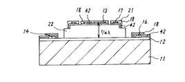
図13にこの発明の赤外線検出装置の第5の実施の形態の断面図を示す。28は赤外線である。実施の形態1の図2に示した断面図において、この発明では空洞23の底面と赤外線検知部13との距離が入射照射される赤外線28の波長の1/4としたものである。例えば赤外線の波長を10μmとすると、赤外線検知部13と空洞23の底との距離は約2.5μmである。
Embodiment 5 FIG.
FIG. 13 shows a cross-sectional view of a fifth embodiment of the infrared detecting device of the present invention.
この製造方法は、予めシリコンのエッチングレートを測定しておき、エッチング深さに対応したエッチング時間を設定する。また後述する実施の形態12、13、14等の方法によりエッチング深さをモニタしながらエッチング深さを赤外線の波長の1/4に形成する。
In this manufacturing method, the etching rate of silicon is measured in advance, and the etching time corresponding to the etching depth is set. Further, the etching depth is formed to ¼ of the infrared wavelength while monitoring the etching depth by the method of
このような構成をとることにより、上方から照射した赤外線が赤外線検知部13を通過し空洞23の底で反射された光が赤外線検知部13の位置で最大の強度となるので、検出感度を向上することができる。
By adopting such a configuration, the infrared ray irradiated from above passes through the
本実施の形態では、実施の形態1に加えて、赤外線検知部と空洞の底部との光学距離を測光波長の1/4としたので、橋部と絶縁部材の2次断面モーメントを上げ、支持体としての剛性を上げるように働くとともに、空洞底面からの反射光の強度を光検知部の位置で最大とするように働く。そのため、赤外線検知部を支持する支持強度の強い構造を提供することができるとともに、更に微細化された赤外線検知部の感度をあげることができる。 In the present embodiment, in addition to the first embodiment, the optical distance between the infrared detecting portion and the bottom of the cavity is set to ¼ of the photometric wavelength, so that the secondary section moment of the bridge portion and the insulating member is increased and supported. It works to increase the rigidity of the body and maximize the intensity of reflected light from the bottom of the cavity at the position of the light detection unit. Therefore, it is possible to provide a structure with strong support strength that supports the infrared detection unit, and it is possible to increase the sensitivity of the further miniaturized infrared detection unit.
実施の形態6.
図14にこの発明の赤外線検出装置の第6の実施の形態の断面図を示す。29は反射膜で、実施の形態1の赤外線検出装置において図2の空洞23の底面に反射膜コートしたものである。
空洞23の底は(100)面の反射率はそれほど高くないので反射膜29により反射率を高めたものである。
FIG. 14 shows a cross-sectional view of a sixth embodiment of the infrared detecting device of the present invention.
Since the reflectance of the (100) plane is not so high at the bottom of the
反射膜29の製造方法は、選択メタルCVD法により行う。例えばWの選択CVDは、6弗化タングステン、水素、シランガスを用いCVD法によりタングステン膜を空洞23の底のシリコン面上に選択的に成長させる。
選択メタルCVD法により形成される他の反射膜29材料としては、モリブデン、アルミニウムも可能である。
このような構成とすることにより、微細な赤外線検知部13の場合でも効率よく検出が可能となる。
The manufacturing method of the
As another
By adopting such a configuration, even a fine
本実施の形態では、実施の形態1に加えて、赤外線検知部の下部のシリコン基板に形成された空洞の底に反射コートを設けるようにしたものである。そのため、橋部或いは絶縁部材の2次断面モーメントを大きくでき、赤外線検知部を支持する支持強度の強い構造を提供することができるとともに、更に微細化された赤外線検知部の感度をあげることができる。 In the present embodiment, in addition to the first embodiment, a reflective coat is provided on the bottom of the cavity formed in the silicon substrate below the infrared detector. Therefore, the secondary section moment of the bridge part or the insulating member can be increased, a structure having a strong support strength for supporting the infrared detection part can be provided, and the sensitivity of the miniaturized infrared detection part can be increased. .
実施の形態7.
実施の形態6では図14に示す反射膜29としてタングステン、モリブデン、アルミニウム等と純金属層を用いたが、WSi2 、TaSi2 、TiSi2 等のシリサイドを用いると
、耐酸化腐食性に強いという効果がある。
この膜の製造方法も選択メタルCVD法を用い、例えばタングステンを空洞23の底に形成した後熱処理してシリサイド化する。
In
This film is also produced by selective metal CVD, for example, by forming tungsten on the bottom of the
実施の形態8.
実施の形態6における反射膜29を金等の膜をメッキ法で形成することができる。
シリコン基板11は導電性があるので、実施の形態2で空洞23まで形成された赤外線検出装置を電解液中に入れ、シリコン基板を陰極としてメッキすると、シリコンの表面が露出している空洞23の底面にのみ金膜を形成することができる。
この方法によれば、CVD装置等が必要なく、製造コストをさげることができる。
The
Since the
According to this method, a CVD apparatus or the like is not necessary, and the manufacturing cost can be reduced.
実施の形態9.
図15および図16に、実施の形態2等における図2の空洞23のエッチング工程において、エッチングが隣接する他の素子にまで広がらないようにするための構造とする一実施の形態を示す。図15において27はエッチングストッパで、分離酸化膜26の下側に形成されたp+層である。
FIGS. 15 and 16 show an embodiment of a structure for preventing etching from spreading to other adjacent elements in the etching process of the
この酸化分離膜26及びエッチングストッパ27の製造方法は、シリコン基板11上に酸化シリコンを形成した後窒化シリコン層を形成し、酸化分離膜26の部分をパターニング除去し、この上から濃度1018〜1020/cm3 のボロンを注入してシリコン基板に厚み0.3〜0.5μmのp+層を形成し、エッチングストッパ27を形成する。つぎにこの基板を酸化処理してエッチングストッパ上に酸化分離膜26を形成する。
Method of manufacturing the
エッチングストッパ27の動作は、酸化分離膜26の下側のシリコン基板11にエッチングが進行しようとしても、濃度1020/cm3 のp+層のエッチングレートはほとんど0であるので、エッチングストッパ27のところでエッチングが停止し、エッチングが横へ広がらないようにする。
この構成をとることにより、図16bに示すような分離酸化層26下へのエッチングの食い込み部分28を生じないので、微小な素子の場合でも隣接する素子との連結を防止することができる。
The
By adopting this configuration, the
本実施の形態では、シリコン基板上に形成された分離酸化膜とその下に形成されたエッチングストッパで区分されたシリコン基板領域内に第1の発明の赤外線検知部を形成するようにしたので、橋部或いは絶縁部材の2次断面モーメントを大きくでき、赤外線検知部を支持する支持強度の強い構造を提供することができるとともに、更に空洞を形成する際に、隣接する赤外線検知部へのエッチングの侵食を小さくでき、微細な赤外線撮像装置が形成できる。これにより微細化した素子間の分離を確実に行うことができる。 In the present embodiment, since the infrared detector of the first invention is formed in the silicon substrate region divided by the isolation oxide film formed on the silicon substrate and the etching stopper formed therebelow, The secondary section moment of the bridge part or the insulating member can be increased, and a structure having a strong support strength for supporting the infrared detection part can be provided. Further, when the cavity is formed, the etching of the adjacent infrared detection part can be performed. Erosion can be reduced and a fine infrared imaging device can be formed. As a result, it is possible to reliably separate the miniaturized elements.
実施の形態10.
この実施の形態においては、実施の形態2に示す図1及び図2の赤外線検出装置の製造方法において、エッチングホール19、20を形成する方向を、エッチングホール19、20の長手方向(図1の上下方向)が、(100)面が表面であるシリコン基板上で<110>方向となるようにしたものである。
このようにするためには、表面が(100)で、ファセットの方向が(110)面のシリコンウエハを用いてエッチングホールの長手方向をファセットに対して平行或いは垂直方向とする。
Embodiment 10 FIG.
In this embodiment, in the method of manufacturing the infrared detecting device of FIGS. 1 and 2 shown in the second embodiment, the direction in which the etching holes 19 and 20 are formed is the longitudinal direction of the etching holes 19 and 20 (see FIG. 1). (Vertical direction) is the <110> direction on the silicon substrate whose (100) plane is the surface.
For this purpose, a silicon wafer having a surface of (100) and a facet direction of (110) is used, and the longitudinal direction of the etching hole is set parallel or perpendicular to the facet.
この実施の形態の動作は、エッチングホールを<110>と平行な直方形とすると、エッチピットはエッチングホールを下底とする逆ピラミット状となるが、<110>方向と傾斜してエッチングホールを形成すると、(100)面はエッチングされ易く、(111)面はエッチングされにくいので、エッチングホールは傾斜した長方形の頂点をむすび<110>に平行な線で結ばれた大きな長方形の孔となってしまう。
このような構成とすることにより、エッチングホールの広がりを少なくすることができる。
In the operation of this embodiment, if the etching hole is a rectangular parallel to <110>, the etch pit has an inverted pyramid shape with the etching hole as a bottom, but the etching hole is inclined with respect to the <110> direction. When formed, the (100) plane is easy to etch and the (111) plane is difficult to etch, so the etching hole is a large rectangular hole connected by a line parallel to <110> that connects the vertices of the inclined rectangle. End up.
With such a configuration, the spread of the etching hole can be reduced.
本実施の形態では、実施の形態1に加えて、マトリクス状に形成する赤外線検知部アレーの形成方法を<110>方向とするようにしたので、橋部或いは絶縁部材の2次断面モーメントが大きくでき、赤外線検知部を支持する支持強度の強い構造を提供するとともに、微細化パターンの広がりのない、高密度な赤外線撮像装置を精度良く形成することができる。 In the present embodiment, in addition to the first embodiment, the method of forming the infrared detector array formed in a matrix is set to the <110> direction, so the secondary section moment of the bridge or the insulating member is large. In addition, it is possible to provide a structure with high support strength that supports the infrared detection unit and to form a high-density infrared imaging device with no spread of a fine pattern with high accuracy.
実施の形態11.
この実施の形態においては、図3で示すように、シリコン基板11上に赤外線検知部13がマトリクス状に配置されて形成される赤外線検出装置の製造方法において、(100)が表面であるシリコン基板11上に、赤外線検知部13の配置方向を<110>方向に平行となるようにしたものである。
この場合も実施の形態13と同様なので、以後の説明を省略する。
In this embodiment, as shown in FIG. 3, in the method of manufacturing an infrared detecting device in which the
This case is the same as that of the thirteenth embodiment, and the description thereof will be omitted.
実施の形態12.
図17はエッチングモニタの一実施の形態を示す図で、第2の実施の形態等の赤外線検知装置の製造方法における図2の赤外線検知部13と空洞23の空洞の底との距離を調節するためのものである。
図17において29は絶縁層で、エッチングされる(100)面を表面とするシリコン基板11上に形成されている。34、35、36はエッチピットで絶縁層29に明けられた〔010〕或いは〔001〕の辺を一辺とする正方形の穴である。
エッチピット35の対角線の長さが目標とするエッチング深さの2倍の寸法で、エッチピット34及び36の対角線長は、エッチピット35のものより短く、或いは長く形成されている。
エッチピット34、35、36は図2のエッチングホール19、20が形成される絶縁膜12、13上で(これが絶縁層29に相当する)エッチングホール19、20の近くに形成される。
FIG. 17 is a diagram showing an embodiment of an etching monitor, and the distance between the
In FIG. 17,
The length of the diagonal line of the
The etch pits 34, 35, and 36 are formed on the insulating
この様なエッチングモニタを設けることにより、エッチング深さは次のように検知することができる。即ち、エッチングホール19、20からエッチングを開始すると、図17に示すように、上方から観察すると、エッチピット34、35、36は、エッチング開始時の工程1ではエッチピットは正方形パターンを示しているが、エッチングが進み目標深さに到達した工程4ではエッチピット34、35に(111)面に交線による対角線が現れる。この時エッチピット36は各角から正方形の中心に向かって部分的に(111)面の交線が延びてきて(100)面に達して止まって台形型パターンとなっている。この時点でエッチングを停止すれば所定の深さの空洞23が得られる。
このようなモニタを設けることにより、目視によりエッチング深さを正確に知ることができる。
By providing such an etching monitor, the etching depth can be detected as follows. That is, when etching is started from the etching holes 19 and 20, as shown in FIG. 17, when viewed from above, the etch pits 34, 35, and 36 show a square pattern in the
By providing such a monitor, the etching depth can be accurately determined visually.
本実施の形態では、シリコン基板上の絶縁層に形成したエッチピットに目標とするエッチング深さで(111)の交線が現れるようにしたので、目視で容易にエッチング深さを知ることができ、異方性エッチの終点検出ができる。これにより上述した空洞の製造段階におけるエッチング深さが確認できる。 In this embodiment, the (111) intersection line appears at the target etching depth in the etch pit formed in the insulating layer on the silicon substrate, so that the etching depth can be easily known visually. The end point of anisotropic etching can be detected. Thereby, the etching depth in the above-described cavity manufacturing stage can be confirmed.
実施の形態13.
図18はエッチングモニタの他の実施の形態を示す図で、第2の実施の形態の赤外線検出装置の製造方法における図2の赤外線検知部13と空洞23の空洞の底との距離を調節するためのものである。
このエッチングモニタの構成も実施の形態12のものと同様に、エッチングされる(100)面を表面とするシリコン基板11上の絶縁層29上に形成された正方形のエッチピット37で構成されている。この実施の形態においては、エッチピット37の対角線長を目標とするエッチング深さの2倍より大きなものとし、更に正方形の各辺の各角からエッチング深さの距離の位置にスリットマーク38を設けるようにしたものである。
FIG. 18 is a diagram showing another embodiment of the etching monitor, in which the distance between the
The configuration of this etching monitor is also composed of square etch pits 37 formed on the insulating
このエッチングモニタの動作は、実施の形態12で示したように、エッチングが開始されると、エッチングモニタ37の各角から正方形の中心に向かって(111)面の交点による筋が現れ、(100)面のところで止まっている。
目標の深さにエッチングが到達すると、正方形の角からの筋はスリットマーク38まで到達するので、この時点でエッチングを停止するようにする。
このような構成をとることにより、目視により容易にエッチング深さを確認することができる。
In the operation of the etching monitor, as shown in the twelfth embodiment, when etching is started, a streak at the intersection of the (111) plane appears from each corner of the etching monitor 37 toward the center of the square, and (100 ) It stops at the surface.
When etching reaches the target depth, the streak from the corner of the square reaches the
By taking such a configuration, the etching depth can be easily confirmed visually.
実施の形態14.
図19はエッチングモニタの更に他の実施の形態の構成を示す図で、第2の実施の形態の赤外線検出装置の製造方法における図2の赤外線検知部13と空洞23の空洞の底との距離を調節するためのものである。
このモニタの構成は、図19に示すように、シリコン基板11の空洞23上の赤外線検知部13上に、空洞23のエッチング中に赤外線28を照射するための赤外線光源39とから構成される。
FIG. 19 is a diagram showing the configuration of still another embodiment of the etching monitor, and the distance between the
As shown in FIG. 19, this monitor is configured by an infrared
このモニタの動作は、空洞23のエッチング中に、赤外線光源39から赤外線28を赤外線検知部13に照射し、その反射光を検知装置(図示せず)でモニタし、その強度が最小となる時点で空洞23のエッチングを停止するようにする。
この点は赤外線検知部13による吸収が最大となる赤外線検知部13と空洞底との距離が照射光の波長の1/4である位置だからである。
このような構成をとることによりエッチング中にエッチング深さを確認することができる。
During the etching of the
This is because the distance between the
By taking such a configuration, the etching depth can be confirmed during etching.
実施の形態15.
以上の実施の形態における空洞23の大部分はシリコン基板11をエッチングして形成されるものであったが、空洞23をシリコン基板11外に形成することもできる。
Although most of the
図20はそのような空洞を形成するプロセスの途中を一画素分について示した立体視図であり、13は赤外線検知部、42は赤外線検知部13をその上に設けた絶縁部材、21は絶縁部材42を脚部50に接続し支持する橋部、22は後にエッチングに除かれて空洞となる犠牲層、14は水平信号線、16は垂直信号線、17は赤外線検知部13の電極であって脚部50、橋部21を通って赤外線検知部13に接続されている。
FIG. 20 is a stereoscopic view showing one pixel in the middle of the process of forming such a cavity, 13 is an infrared detector, 42 is an insulating member provided with the
図21は図20のAA線に沿った断面図である。橋部21を形成する絶縁層42、21の断面形状は、犠牲層22の段差が転写されることにより、L字型の段差のある形状となり、機械的に強化された構造となっている。このような段差を絶縁層に作る為に犠牲層22も2段形状となっている。11はシリコン基板、12は絶縁層である。赤外線検知部13と絶縁層12との距離は入射する赤外光の波長の1/4に形成されている。絶縁層12の表面には反射コートが設けられる。
FIG. 21 is a sectional view taken along line AA in FIG. The cross-sectional shape of the insulating
図22は完成した一画素分の平面図である。
図23は図20の主要部とその断面図を示すもので、(a)は斜視図、(b)はBB線に沿った断面図、(c)はAA線に沿った断面図、(d)は橋部21と脚部50だけの斜視図である。犠牲層22が2段形状となっており、犠牲層22の段の部分で橋部21の断面形状がL字型となり剛性が高められている。脚部50を犠牲層22の角に形成したので機械的に強くなっている。
FIG. 22 is a plan view of one completed pixel.
FIG. 23 shows the main part of FIG. 20 and a cross-sectional view thereof, (a) is a perspective view, (b) is a cross-sectional view along the BB line, (c) is a cross-sectional view along the AA line, (d ) Is a perspective view of only the
図24(a)〜(k)は、図20〜23に示す素子の製造プロセスの説明図である。(a)はシリコン基板11の主表面上の厚さ6000Åの絶縁膜SiO2 12の上に犠牲層22を形成した状態である。犠牲層22はCVD法により多結晶シリコンを積層して形成する。
24A to 24K are explanatory diagrams of the manufacturing process of the element shown in FIGS. (A) shows a state in which a
次いで、(b)、(c)のようにレジストパターン54を形成して犠牲層22をドライエッチングして段差を作る。この実施の形態では段差は2μmに形成した。更に(d)、(e)、(f)において、レジストパターンを形成し、犠牲層22を形成する。犠牲層22の厚さは入射赤外光の波長の1/4とする。
絶縁膜12上に厚さ5000Åのアルミニウムでスパッタ法により水平、垂直信号線を形成した後、赤外線検知部を載せる絶縁部材42となる絶縁層を犠牲層22を覆って形成した状態が(g)である。絶縁部材42は例えばCVD法によりSiO2 で1000Åの厚さで形成される。
Next, as shown in (b) and (c), a resist
After forming horizontal and vertical signal lines on the insulating
次いで、水素を含有したCVD法による非晶質シリコンで赤外線検知部13を、スパッタ法により500Åの厚さのタングステンで電極17を夫々形成する。その上のCVD法により窒化シリコン膜18を2000Åの厚さに形成する。この状態を(b)に示す。
次いで、レジストパターンを形成し(i)、ドライエッチングによりエッチホール19を形成する(j)。最後にエッチンホール19を通して犠牲層22の多結晶シリコンを溶出させ空洞23を作る(k)。橋部21の断面形状はL字型で剛性が高められている。
Next, the
Next, a resist pattern is formed (i), and an
本実施の形態では、シリコン基板上の犠牲層に段差パターンを設け、その上に絶縁部材を設けるので、段差パターンが絶縁部材に転写され、赤外線検知部を搭載する絶縁部材、脚部およびそれを保持する橋部の少なくとも一つの断面形状が段差を有するようになる。そのため、橋部或いは絶縁部材の2次断面モーメントを大きくでき、赤外線検知部を支持する支持強度の強い構造を提供することができる。 In this embodiment, the step pattern is provided on the sacrificial layer on the silicon substrate, and the insulating member is provided thereon. Therefore, the step pattern is transferred to the insulating member, and the insulating member, the leg portion, and the insulating member on which the infrared detection unit is mounted. At least one cross-sectional shape of the bridge portion to be held has a step. Therefore, the secondary section moment of the bridge part or the insulating member can be increased, and a structure having a strong support strength for supporting the infrared detection part can be provided.
実施の形態16.
空洞23をシリコン基板11外に形成し、且つ橋部の断面形状をT字型として剛性を高める実施の形態を図25、図26に基いて説明する。
An embodiment in which the
図25は、犠牲層22上に橋部21および絶縁部材42を形成した状態を示す図で(a)は斜視図、(b)はAA線に沿った断面図、(c)はCC線に沿った断面図である。橋部21および絶縁部材42の断面形状はT字型であり、剛性が高められている。
25A and 25B are views showing a state in which the
図26(a)〜(g)は、この実施の形態の製造過程の説明図である。(a)はシリコン基板11上にCVD法により厚さ6000Åの酸化シリコン膜を形成し、更に多結晶シリコンにより犠牲層22を形成し、犠牲層22上にレジストパターン54を形成した状態を示す。
FIGS. 26A to 26G are explanatory diagrams of the manufacturing process of this embodiment. (A) shows a state in which a silicon oxide film having a thickness of 6000 mm is formed on the
次に、ドライエッチングにより多結晶シリコン層22に凹型の段差47を形成する(b)。その上に更にレジストパターン54を形成し(c)、ドライエッチングを行い犠牲層22を形成する(d)。
Next, a
水平信号線16を例えばAlのスパッタにより厚さ5000Åに形成した後、犠牲層22を含め全面にCVD法により厚さ1000Åの酸化シリコン膜を形成する。その上にCVD法により水素を含む非晶質シリコンで赤外線検知部13を、スパッタ法によりタングステン電極17を形成する(e)。
その上から、CVD法によりSiN膜18を形成する(e)。
After forming the
Then, a
次に、レジストパターン(図示せず)を形成し、SiN膜18とSiO2 絶縁膜42を選択的にエッチングしてエッチングホール19を形成する(f)。エッチングホール19を通して犠牲層ポリシリコン22をKOH溶液で溶出させて空洞23を形成する(g)。橋部21および検知部13を載せる絶縁部材42は断面形状がT字型に形成され、剛性が高められている。
Next, a resist pattern (not shown) is formed, and the
実施の形態17.
空洞23をシリコン基板11外に形成し、且つ、橋部の断面形状を逆U字型として剛性を高めた実施の形態の製造過程を図27(a)〜(f)に基いて説明する。
The manufacturing process of the embodiment in which the
シリコン基板11上にSiO2 絶縁膜12とポリシリコンの犠牲層22を形成し、更に、犠牲層22上にレジストパターン54を形成する(a)。
犠牲層22を選択エッチングして表面に凸形状の段差を形成した後、更にレジストパターン54を形成し(b)、エッチングして犠牲層22を得る(c)。次に、犠牲層22を覆ってSiO2 膜を形成し、その上に非晶質シリコンの赤外線検知部とタングステン電極を形成し、更にSiN膜を形成する(d)。レジストパターンを形成し、選択エッチングによりエッチングホールを形成し(e)、エッチングホールを通してKOH溶液により犠牲層22を溶かし出して空洞23を形成する(f)。
橋部21および絶縁部材42は逆U字型となっているので剛性が高められている。
An SiO 2 insulating film 12 and a polysilicon
After selectively etching the
Since the
実施の形態18.
空洞23をシリコン基板11外に形成し、且つ橋部の断面形状をL字型とする他の実施の形態を図28、図29について説明する。
Another embodiment in which the
図28(a)は一画素分の主要部の犠牲層エッチング前の斜視図、図28(b)は図28(a)のBB線に沿った断面図、図28(c)は図28(a)のAA線に沿った断面図である。この実施の形態では犠牲層22は台形に形成される。橋部21は変型したL字型に形成される。
FIG. 28A is a perspective view of a main portion of one pixel before etching a sacrificial layer, FIG. 28B is a cross-sectional view taken along line BB in FIG. 28A, and FIG. It is sectional drawing along the AA line of a). In this embodiment, the
図29(a)〜(f)は、製造過程の説明図である。
シリコン基板11上にSiO2 膜12を形成し、その上にポリシリコンの犠牲層22を形成しレジストパターン54を形成する(a)。SF6 ガスにより等方性のドライエッチングを行い、台形の犠牲層22を形成する(b)、(c)。信号線16を形成した後、全面にSiO2 絶縁膜42を形成し、その上に非晶質シリコンの赤外線検知部13、タングステン電極17を形成し、更にSiN膜18を形成する。その後レジストパターンを形成し、エッチングホール19を形成し(d)、エッチングホール19を通してKOH溶液により犠牲層22を溶出させ、空洞23を形成する。
橋部21は変型したL字型に形成されているので剛性が高められている。
FIGS. 29A to 29F are explanatory diagrams of the manufacturing process.
A SiO 2 film 12 is formed on the
Since the
以上のように説明した実施の形態15から18では、犠牲層の段差パターンを台形、凹状または凸状としたので、絶縁部材の断面形状を剛性の高い変型L字型、T字型または逆U字型にできる。そのため、段差パターンが絶縁部材等に転写され、赤外線検知部を搭載する絶縁部材、脚部およびそれを保持する橋部の少なくとも一つの断面形状が段差を有するようになる。そのため、橋部或いは絶縁部材の2次断面モーメントを大きくでき、赤外線検知部を支持する支持強度の強い構造を提供することができる。 In the fifteenth to eighteenth embodiments described above, the step pattern of the sacrificial layer is trapezoidal, concave or convex, so that the cross-sectional shape of the insulating member is a highly rigid L-shaped, T-shaped or inverted U. Can be shaped like a letter. Therefore, the step pattern is transferred to an insulating member or the like, and at least one cross-sectional shape of the insulating member on which the infrared detection unit is mounted, the leg portion, and the bridge portion holding the step has a step. Therefore, the secondary section moment of the bridge part or the insulating member can be increased, and a structure having a strong support strength for supporting the infrared detection part can be provided.
赤外線検知部13には各種赤外線センサが採用可能である。赤外線によって検知膜の抵抗が変化し、これを電流の変化として検知するボロメータ方式の熱赤外センサの他に熱電対型の赤外センサや焦電型の赤外センサも使用できる。
Various infrared sensors can be used for the
11 シリコン基板 12 絶縁層
13 赤外線検知部 15 電極
17 電極 18 絶縁層
19 エッチングホール 20 エッチングホール
21 橋部 22 犠牲層
23 空洞 26 分離酸化膜
27 エッチングストッパ 28 反射コート
29 絶縁層 34 エッチピット
35 エッチピット 36 エッチピット
37 エッチピット 38 スリットマーク
42 絶縁部材 46 犠牲層
47 凹部の段差パターン
DESCRIPTION OF
Claims (3)
Priority Applications (1)
| Application Number | Priority Date | Filing Date | Title |
|---|---|---|---|
| JP2009174251A JP5386729B2 (en) | 1995-02-16 | 2009-07-27 | Infrared detector |
Applications Claiming Priority (3)
| Application Number | Priority Date | Filing Date | Title |
|---|---|---|---|
| JP1995028251 | 1995-02-16 | ||
| JP2825195 | 1995-02-16 | ||
| JP2009174251A JP5386729B2 (en) | 1995-02-16 | 2009-07-27 | Infrared detector |
Related Parent Applications (1)
| Application Number | Title | Priority Date | Filing Date |
|---|---|---|---|
| JP2006310423A Division JP4400615B2 (en) | 1995-02-16 | 2006-11-16 | Infrared detector manufacturing method |
Publications (2)
| Publication Number | Publication Date |
|---|---|
| JP2009244282A JP2009244282A (en) | 2009-10-22 |
| JP5386729B2 true JP5386729B2 (en) | 2014-01-15 |
Family
ID=41306302
Family Applications (1)
| Application Number | Title | Priority Date | Filing Date |
|---|---|---|---|
| JP2009174251A Expired - Lifetime JP5386729B2 (en) | 1995-02-16 | 2009-07-27 | Infrared detector |
Country Status (1)
| Country | Link |
|---|---|
| JP (1) | JP5386729B2 (en) |
Families Citing this family (4)
| Publication number | Priority date | Publication date | Assignee | Title |
|---|---|---|---|---|
| JP5589605B2 (en) * | 2010-06-25 | 2014-09-17 | セイコーエプソン株式会社 | Pyroelectric detector, pyroelectric detector and electronic device |
| JP2012059881A (en) * | 2010-09-08 | 2012-03-22 | Toshiba Corp | Imaging device, imaging module and method for manufacturing imaging device |
| EP2806456A4 (en) | 2012-03-29 | 2015-03-18 | Asahi Kasei Microdevices Corp | Light receiving device |
| JP5766145B2 (en) * | 2012-03-29 | 2015-08-19 | 旭化成エレクトロニクス株式会社 | Infrared sensor array |
Family Cites Families (4)
| Publication number | Priority date | Publication date | Assignee | Title |
|---|---|---|---|---|
| JPH0697188B2 (en) * | 1986-06-03 | 1994-11-30 | 松下電器産業株式会社 | Infrared detector and manufacturing method thereof |
| JPH03287022A (en) * | 1990-04-02 | 1991-12-17 | Matsushita Electric Works Ltd | Infrared detecting element, infrared detector and production of infrared detecting element |
| JPH04158583A (en) * | 1990-10-22 | 1992-06-01 | Matsushita Electric Works Ltd | Infrared-ray detecting element |
| JP2633124B2 (en) * | 1991-10-25 | 1997-07-23 | 山武ハネウエル株式会社 | Diaphragm sensor |
-
2009
- 2009-07-27 JP JP2009174251A patent/JP5386729B2/en not_active Expired - Lifetime
Also Published As
| Publication number | Publication date |
|---|---|
| JP2009244282A (en) | 2009-10-22 |
Similar Documents
| Publication | Publication Date | Title |
|---|---|---|
| JP3811964B2 (en) | Infrared detector and manufacturing method thereof | |
| JP4009046B2 (en) | Infrared sensor | |
| US6552344B1 (en) | Infrared detector and method of making the infrared detector | |
| EP2375228B1 (en) | Optical sensor | |
| EP2105963A2 (en) | Infrared detector and solid state image sensor having the same | |
| US6198098B1 (en) | Microstructure for infrared detector and method of making same | |
| JP4792980B2 (en) | Infrared detector | |
| JP5386729B2 (en) | Infrared detector | |
| US20070252085A1 (en) | Photovoltage Detector | |
| JP3925556B2 (en) | Infrared imaging device and manufacturing method thereof | |
| JPH02205729A (en) | Infrared-ray sensor | |
| JP4400615B2 (en) | Infrared detector manufacturing method | |
| US6579740B2 (en) | Method of making a thin film sensor | |
| JPH07283444A (en) | Manufacture of infrared detector | |
| JP2910448B2 (en) | Infrared sensor | |
| JP3132197B2 (en) | Thermal infrared sensor | |
| JP2568292B2 (en) | Thermo-pile type infrared sensor | |
| JP3809718B2 (en) | Infrared detector | |
| JP2010101675A (en) | Infrared imaging element and method of manufacturing the same | |
| JP2884679B2 (en) | Thermopile type infrared sensor | |
| JP2000111396A (en) | Infrared detecting element and its manufacture | |
| KR100497333B1 (en) | Pixel array for Detector with thin film transistor and method for fabrication of the same | |
| JP5669654B2 (en) | Infrared imaging device manufacturing method and infrared imaging device | |
| JP3840768B2 (en) | Semiconductor device and manufacturing method of semiconductor device | |
| JPH08261832A (en) | Infrared sensor and its manufacture |
Legal Events
| Date | Code | Title | Description |
|---|---|---|---|
| A621 | Written request for application examination |
Free format text: JAPANESE INTERMEDIATE CODE: A621 Effective date: 20090727 |
|
| A131 | Notification of reasons for refusal |
Free format text: JAPANESE INTERMEDIATE CODE: A131 Effective date: 20110802 |
|
| A521 | Written amendment |
Free format text: JAPANESE INTERMEDIATE CODE: A523 Effective date: 20110907 |
|
| A131 | Notification of reasons for refusal |
Free format text: JAPANESE INTERMEDIATE CODE: A131 Effective date: 20120214 |
|
| A521 | Written amendment |
Free format text: JAPANESE INTERMEDIATE CODE: A523 Effective date: 20120411 |
|
| A131 | Notification of reasons for refusal |
Free format text: JAPANESE INTERMEDIATE CODE: A131 Effective date: 20121204 |
|
| A521 | Written amendment |
Free format text: JAPANESE INTERMEDIATE CODE: A523 Effective date: 20130111 |
|
| TRDD | Decision of grant or rejection written | ||
| A01 | Written decision to grant a patent or to grant a registration (utility model) |
Free format text: JAPANESE INTERMEDIATE CODE: A01 Effective date: 20130903 |
|
| A61 | First payment of annual fees (during grant procedure) |
Free format text: JAPANESE INTERMEDIATE CODE: A61 Effective date: 20130916 |
|
| EXPY | Cancellation because of completion of term |