JP5386079B2 - Display device - Google Patents
Display device Download PDFInfo
- Publication number
- JP5386079B2 JP5386079B2 JP2007327185A JP2007327185A JP5386079B2 JP 5386079 B2 JP5386079 B2 JP 5386079B2 JP 2007327185 A JP2007327185 A JP 2007327185A JP 2007327185 A JP2007327185 A JP 2007327185A JP 5386079 B2 JP5386079 B2 JP 5386079B2
- Authority
- JP
- Japan
- Prior art keywords
- circuit
- unit
- display
- display device
- signal
- Prior art date
- Legal status (The legal status is an assumption and is not a legal conclusion. Google has not performed a legal analysis and makes no representation as to the accuracy of the status listed.)
- Expired - Fee Related
Links
Images


Classifications
-
- G—PHYSICS
- G09—EDUCATION; CRYPTOGRAPHY; DISPLAY; ADVERTISING; SEALS
- G09G—ARRANGEMENTS OR CIRCUITS FOR CONTROL OF INDICATING DEVICES USING STATIC MEANS TO PRESENT VARIABLE INFORMATION
- G09G3/00—Control arrangements or circuits, of interest only in connection with visual indicators other than cathode-ray tubes
- G09G3/20—Control arrangements or circuits, of interest only in connection with visual indicators other than cathode-ray tubes for presentation of an assembly of a number of characters, e.g. a page, by composing the assembly by combination of individual elements arranged in a matrix no fixed position being assigned to or needed to be assigned to the individual characters or partial characters
- G09G3/2092—Details of a display terminals using a flat panel, the details relating to the control arrangement of the display terminal and to the interfaces thereto
- G09G3/2096—Details of the interface to the display terminal specific for a flat panel
-
- H—ELECTRICITY
- H04—ELECTRIC COMMUNICATION TECHNIQUE
- H04N—PICTORIAL COMMUNICATION, e.g. TELEVISION
- H04N5/00—Details of television systems
- H04N5/44—Receiver circuitry for the reception of television signals according to analogue transmission standards
-
- G—PHYSICS
- G06—COMPUTING; CALCULATING OR COUNTING
- G06F—ELECTRIC DIGITAL DATA PROCESSING
- G06F3/00—Input arrangements for transferring data to be processed into a form capable of being handled by the computer; Output arrangements for transferring data from processing unit to output unit, e.g. interface arrangements
- G06F3/14—Digital output to display device ; Cooperation and interconnection of the display device with other functional units
- G06F3/147—Digital output to display device ; Cooperation and interconnection of the display device with other functional units using display panels
-
- G—PHYSICS
- G09—EDUCATION; CRYPTOGRAPHY; DISPLAY; ADVERTISING; SEALS
- G09G—ARRANGEMENTS OR CIRCUITS FOR CONTROL OF INDICATING DEVICES USING STATIC MEANS TO PRESENT VARIABLE INFORMATION
- G09G3/00—Control arrangements or circuits, of interest only in connection with visual indicators other than cathode-ray tubes
- G09G3/20—Control arrangements or circuits, of interest only in connection with visual indicators other than cathode-ray tubes for presentation of an assembly of a number of characters, e.g. a page, by composing the assembly by combination of individual elements arranged in a matrix no fixed position being assigned to or needed to be assigned to the individual characters or partial characters
- G09G3/2092—Details of a display terminals using a flat panel, the details relating to the control arrangement of the display terminal and to the interfaces thereto
-
- G—PHYSICS
- G09—EDUCATION; CRYPTOGRAPHY; DISPLAY; ADVERTISING; SEALS
- G09G—ARRANGEMENTS OR CIRCUITS FOR CONTROL OF INDICATING DEVICES USING STATIC MEANS TO PRESENT VARIABLE INFORMATION
- G09G2330/00—Aspects of power supply; Aspects of display protection and defect management
- G09G2330/02—Details of power systems and of start or stop of display operation
-
- G—PHYSICS
- G09—EDUCATION; CRYPTOGRAPHY; DISPLAY; ADVERTISING; SEALS
- G09G—ARRANGEMENTS OR CIRCUITS FOR CONTROL OF INDICATING DEVICES USING STATIC MEANS TO PRESENT VARIABLE INFORMATION
- G09G2370/00—Aspects of data communication
- G09G2370/16—Use of wireless transmission of display information
-
- G—PHYSICS
- G09—EDUCATION; CRYPTOGRAPHY; DISPLAY; ADVERTISING; SEALS
- G09G—ARRANGEMENTS OR CIRCUITS FOR CONTROL OF INDICATING DEVICES USING STATIC MEANS TO PRESENT VARIABLE INFORMATION
- G09G2380/00—Specific applications
- G09G2380/04—Electronic labels
-
- G—PHYSICS
- G09—EDUCATION; CRYPTOGRAPHY; DISPLAY; ADVERTISING; SEALS
- G09G—ARRANGEMENTS OR CIRCUITS FOR CONTROL OF INDICATING DEVICES USING STATIC MEANS TO PRESENT VARIABLE INFORMATION
- G09G2380/00—Specific applications
- G09G2380/06—Remotely controlled electronic signs other than labels
-
- H—ELECTRICITY
- H04—ELECTRIC COMMUNICATION TECHNIQUE
- H04N—PICTORIAL COMMUNICATION, e.g. TELEVISION
- H04N5/00—Details of television systems
- H04N5/66—Transforming electric information into light information
Description
本発明は、画像を表示するための表示装置に係り、特に無線技術を用いてデータ通信を行う表示装置に関する。 The present invention relates to a display device for displaying an image, and more particularly to a display device that performs data communication using wireless technology.
近年、高度情報化社会の到来に伴い、コンピュータ、ナビゲーションシステム、携帯情報端末、情報通信機器あるいはこれらの複合製品の需要が増大している。これらの製品の表示手段には、薄型、軽量、低消費電力の表示装置が適しており、液晶表示装置あるいは自発光型のEL素子またはLEDなどの電気光学素子を用いた表示装置が用いられている。 In recent years, with the advent of an advanced information society, demand for computers, navigation systems, portable information terminals, information communication devices, or composite products of these has increased. As the display means of these products, a thin, lightweight, low power consumption display device is suitable, and a liquid crystal display device or a display device using an electro-optical element such as a self-luminous EL element or LED is used. Yes.
これらの表示装置は、駆動するための電源を内蔵し、FPC(フレキシブルプリント回路)あるいはケーブルによって、外部から映像信号を供給するという方法が用いられてきた。 These display devices incorporate a power source for driving, and a method of supplying a video signal from the outside through an FPC (flexible printed circuit) or a cable has been used.
しかし、表示装置の使用環境や用途によっては電源を内蔵することで外形サイズの増加や発熱等の問題が多大な影響を与える可能性があり、また、映像や画像といった映像コンテンツの提供は、表示装置に直接接続されたFPCやケーブルによってなされるが、経年劣化や機械的ストレス等によるFPC、ケーブルの断線といった問題を生じる恐れがある。 However, depending on the usage environment and application of the display device, there is a possibility that problems such as an increase in external size and heat generation will have a significant impact by incorporating a power supply. Although it is done by FPC or cable directly connected to the apparatus, there is a possibility that problems such as FPC and cable disconnection due to aging deterioration or mechanical stress may occur.
そこで、上述の問題を解決する手段として、特許文献1には、映像信号を表示装置に直接接続入力するためのFPCやケーブル等の入力/出力端子を必要としない表示装置について提案がなされている。
前述の特許文献1に記載されている表示装置では、画像信号を無線手段である電波、あるいは、光を使ってワイヤレスに入力が行われ、表示装置を駆動するための電力が電磁波を用いて供給されている。 In the display device described in Patent Document 1 described above, an image signal is input wirelessly using radio waves or light as wireless means, and power for driving the display device is supplied using electromagnetic waves. Has been.
しかしながら、前述の特許文献1では、表示装置は画像信号を受信するのみで送信はしない機構である。そのため、別途配置された画像信号発信装置側でなければ、実施者が所望する設定や表示画像などを、表示装置側からフィードバックすることが出来ないという問題点がある。 However, in Patent Document 1 described above, the display device is a mechanism that only receives an image signal and does not transmit it. Therefore, there is a problem that settings and display images desired by the practitioner cannot be fed back from the display device side unless the image signal transmission device is separately arranged.
また、画像信号発信装置から提供される画像は、画像信号発信装置で設定した一種のみで、同時に複数の表示画像が提供されることは無く、実施者が複数存在した場合には、各実施者の所望する設定や表示画像などを提供するために、同数の画像信号発信装置を用意する必要がある。 In addition, the image provided from the image signal transmission device is only one type set by the image signal transmission device, and a plurality of display images are not provided at the same time. It is necessary to prepare the same number of image signal transmission devices in order to provide the desired settings and display images.
本発明は前述の課題に鑑みてなされたものであり、映像信号を表示装置に直接接続入力するためのFPCやケーブル等の入力/出力端子を必要とせず、実施者の所望する設定や表示画像などを提供できる表示装置を提供するものである。 The present invention has been made in view of the above-described problems, and does not require an input / output terminal such as an FPC or a cable for directly connecting and inputting a video signal to a display device. The display apparatus which can provide etc. is provided.
本発明の表示装置は、情報を書き換えて表示する表示部と、無線信号を送信及び受信するためのアンテナ部と、受信した情報に対する実施者からの要求をデータ送受信器へ送るため、アンテナ部で受信した無線信号を電力へと変換し、各回路の駆動に必要な電力を保持及び供給するバッテリー部と、アンテナ部で受信した無線信号を画像信号へと変換して表示部に供給し、且つ実施者からの要求を満たすための命令を無線信号へと変換しアンテナ部からデータ送受信器へ送信を行うためのコントローラ部と、実施者が要求を入力するためのコンソール部と、を有することを特徴とする。 The display device of the present invention includes a display unit that rewrites and displays information, an antenna unit for transmitting and receiving radio signals, and an antenna unit for sending a request from a practitioner for received information to a data transceiver. The received wireless signal is converted into electric power, a battery unit that holds and supplies electric power necessary for driving each circuit, the wireless signal received by the antenna unit is converted into an image signal and supplied to the display unit, and It has a controller unit for converting a command for satisfying a request from the practitioner into a radio signal and transmitting it from the antenna unit to the data transceiver, and a console unit for the practitioner to input the request. Features.
本発明の表示装置は、データ送受信器から送信される無線信号をワイヤレスで受け取り、情報の表示を行うことができる。また、本発明の表示装置は、実施者からの要求を表示装置からデータ送受信器へ送信し再度データ送受信器から表示装置に無線信号を送信させることによって所望の情報を受け取ることが可能となる。 The display device of the present invention can wirelessly receive a radio signal transmitted from a data transceiver and display information. In addition, the display device of the present invention can receive desired information by transmitting a request from the practitioner from the display device to the data transmitter / receiver and again transmitting a radio signal from the data transmitter / receiver to the display device.
本発明によれば、本発明の無線技術を用いた表示装置が無線信号を受信できる環境にあり、且つ表示装置にて画像の表示を行っていない場合、バッテリーに電力を充電でき、さらに表示装置からデータ送受信器へ無線信号を送信する際にバッテリーに蓄えられた電力を利用するため、通信可能距離が拡大する。 According to the present invention, when the display device using the wireless technology of the present invention is in an environment where a wireless signal can be received and no image is displayed on the display device, the battery can be charged with power, and the display device Because the electric power stored in the battery is used when transmitting a radio signal from the transmitter to the data transmitter / receiver, the communicable distance is expanded.
また、本発明の無線技術を用いた表示装置は、情報を書き換えて表示する表示部と、無線信号を送信及び受信するためのアンテナ部と、受信した情報に対する実施者からの要求をデータ送受信器へ送るため、その命令を格納する記憶装置部と、アンテナ部で受信した無線信号を電力へと変換し、各回路の駆動に必要な電力を保持及び供給するバッテリー部と、アンテナ部で受信した無線信号を画像信号へと変換して表示部に供給し、且つ実施者からの要求を満たすための命令を無線信号へと変換しアンテナ部からデータ送受信器へ送信を行うためのコントローラ部と、実施者が要求を入力するためのコンソール部と、を有し、上記構成要素を同一基板上に形成することを特徴とする。 In addition, a display device using the wireless technology of the present invention includes a display unit that rewrites and displays information, an antenna unit for transmitting and receiving wireless signals, and a data transmitter / receiver that requests a practitioner for received information. The battery unit that stores the command, the battery unit that converts the radio signal received by the antenna unit into power, and holds and supplies the power necessary for driving each circuit, and the antenna unit A controller unit for converting a radio signal into an image signal and supplying it to the display unit, and converting a command for satisfying a request from the practitioner into a radio signal and transmitting the signal from the antenna unit to the data transceiver; And a console unit for a practitioner to input a request, and the above-described components are formed on the same substrate.
本発明によれば、無線技術を用いた表示装置の部品点数が削減でき、低コスト化が可能となる。 According to the present invention, the number of components of a display device using wireless technology can be reduced, and the cost can be reduced.
本発明によれば、無線信号を受信可能であったとしてもデータ送受信器との距離の増加に応じた信号の減衰が生じて、表示装置に画像が表示できなかった距離においても表示可能となる範囲が拡大する。 According to the present invention, even if a wireless signal can be received, the signal is attenuated as the distance to the data transmitter / receiver increases, and the image can be displayed at a distance where the image cannot be displayed on the display device. The range expands.
本発明の表示装置は、映像信号を表示装置に直接接続入力するためのFPCやケーブル等の入力/出力端子を必要とせず、無線信号を利用して動作を行うことができるため、FPCの劣化またはケーブルの断線等の不具合がなく、信頼性を向上させることができる。 The display device of the present invention does not require an input / output terminal such as an FPC or a cable for directly connecting and inputting a video signal to the display device, and can operate using a radio signal. Or there is no malfunction, such as a cable disconnection, and it can improve reliability.
また本発明の表示装置は、コンソール部より入力された信号を外部に無線信号として送信することができる。そのため表示装置において、実施者の所望する設定や表示画像などを外部の画像信号発信装置より送信させることが可能となる。 The display device of the present invention can transmit a signal input from the console unit to the outside as a radio signal. Therefore, in the display device, settings desired by the practitioner, display images, and the like can be transmitted from an external image signal transmission device.
以下、本発明の実施の形態及び実施例において図面を参照しながら説明する。但し、本発明は多くの異なる態様で実施することが可能であり、本発明の趣旨及びその範囲から逸脱することなくその形態及び詳細を様々に変更し得ることは当業者であれば容易に理解される。従って、本実施の形態及び実施例の記載内容に限定して解釈されるものではない。なお、実施の形態を説明するための全図において、同一部分又は同様な機能を有する部分には同一の符号を付し、その繰り返しの説明は省略する。
(実施の形態1)
Hereinafter, embodiments and examples of the present invention will be described with reference to the drawings. However, the present invention can be implemented in many different modes, and those skilled in the art can easily understand that the modes and details can be variously changed without departing from the spirit and scope of the present invention. Is done. Therefore, the present invention is not construed as being limited to the description of the embodiments and examples. Note that in all the drawings for describing the embodiments, the same portions or portions having similar functions are denoted by the same reference numerals, and repetitive description thereof is omitted.
(Embodiment 1)
本発明の表示装置は、映像信号を表示装置に直接接続入力するためのFPCやケーブル等の入力/出力端子を必要とせず、無線信号を利用して動作を行うものである。以下、本発明の表示装置の構成について説明する。 The display device of the present invention does not require an input / output terminal such as an FPC or a cable for directly connecting and inputting a video signal to the display device, and operates using a radio signal. Hereinafter, the configuration of the display device of the present invention will be described.
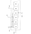
図1に示すように表示装置100は、表示部101と、コントローラ部102と、アンテナ部103と、バッテリー部104と、コンソール部105と、で構成される。
As shown in FIG. 1, the
また表示装置100は、図7に示すように、データ送受信器701より無線信号702を供給される。データ送受信器701からの無線信号702により表示装置100は電力の供給及びデータの受信をおこなうことができる。また、データ送受信器701は、表示装置100から送信される無線信号703を受信し、受信した信号に応じて無線信号を送信するものである。
Further, as shown in FIG. 7, the
図1における表示部101について図2に説明する。表示部101は、表示素子がマトリクス状に配置された表示面201と、表示面201に画像を表示させるための駆動回路202とを有する。表示部101は、バッテリーより出力される電力を用いて、コントローラ部より入力される画像信号を駆動回路202で処理し、表示面201に画像を表示させる。
The
なお、表示部101は、画素に能動素子を有するアクティブマトリクス方式の表示パネル、画素に能動素子を有しないパッシブマトリクス方式の表示パネルを用いることができる。
Note that the
アクティブマトリクス方式では、能動素子(アクティブ素子、非線形素子)として、トランジスタだけでなく、さまざまな能動素子(アクティブ素子、非線形素子)を用いることが出来る。例えば、MIM(Metal Insulator Metal)やTFD(Thin Film Diode)などを用いることも可能である。これらの素子は、製造工程が少ないため、製造コストの低減、及び歩留まりの向上を図ることができる。さらに、素子のサイズが小さいため、開口率を向上させることができ、低消費電力化や高輝度化をはかることが出来る。 In the active matrix system, not only transistors but also various active elements (active elements and nonlinear elements) can be used as active elements (active elements and nonlinear elements). For example, MIM (Metal Insulator Metal) or TFD (Thin Film Diode) can be used. Since these elements have few manufacturing processes, the manufacturing cost can be reduced and the yield can be improved. Furthermore, since the size of the element is small, the aperture ratio can be improved, and low power consumption and high luminance can be achieved.
なお、アクティブマトリクス方式以外のものとして、能動素子(アクティブ素子、非線形素子)を用いないパッシブマトリクス型を用いることも可能である。能動素子(アクティブ素子、非線形素子)を用いないため、製造工程が少なく、製造コストの低減、又は歩留まりの向上を図ることができる。また、開口率を向上させることができ、低消費電力化や高輝度化をはかることが出来る。 Note that as a method other than the active matrix method, a passive matrix type that does not use active elements (active elements, nonlinear elements) can be used. Since no active element (active element or nonlinear element) is used, the number of manufacturing steps is small, and manufacturing cost can be reduced or yield can be improved. In addition, the aperture ratio can be improved, and low power consumption and high luminance can be achieved.
なお表示部における表示素子としては、EL素子(有機物及び無機物を含むEL素子、有機EL素子、無機EL素子)、電子放出素子、液晶素子、電子インク、電気泳動素子、グレーティングライトバルブ(GLV)、プラズマディスプレイ(PDP)、デジタルマイクロミラーデバイス(DMD)、圧電セラミックディスプレイ、カーボンナノチューブ、など、電気磁気的作用により、コントラスト、輝度、反射率、透過率などが変化する表示媒体を用いることができる。なお、EL素子を用いた表示装置としてはELディスプレイ、電子放出素子を用いた表示装置としてはフィールドエミッションディスプレイ(FED)やSED方式平面型ディスプレイ(SED:Surface−conduction Electron−emitter Disply)など、液晶素子を用いた表示装置としては液晶ディスプレイ(透過型液晶ディスプレイ、半透過型液晶ディスプレイ、反射型液晶ディスプレイ、直視型液晶ディスプレイ、投射型液晶ディスプレイ)、電子インクや電気泳動素子を用いた表示装置としては電子ペーパーがある。 Note that as a display element in the display unit, an EL element (an EL element including an organic substance and an inorganic substance, an organic EL element, an inorganic EL element), an electron-emitting element, a liquid crystal element, electronic ink, an electrophoretic element, a grating light valve (GLV), A display medium such as a plasma display (PDP), a digital micromirror device (DMD), a piezoelectric ceramic display, a carbon nanotube, or the like that changes contrast, luminance, reflectance, transmittance, and the like due to an electromagnetic action can be used. Note that a display device using an EL element is an EL display, and a display device using an electron-emitting device is a liquid crystal display such as a field emission display (FED) or a SED type flat display (SED: Surface-conduction Electron-Emitter Display). Liquid crystal displays (transmission type liquid crystal display, transflective type liquid crystal display, reflection type liquid crystal display, direct view type liquid crystal display, projection type liquid crystal display), display devices using electronic ink and electrophoretic elements There is electronic paper.
図1におけるコントローラ部102の構成について図3を用いて説明する。
The configuration of the
図3に示す処理回路301は、表示装置100内で生成された信号を処理する回路である。また記憶回路302は表示装置100内で生成された信号を一時的に記憶するための回路である。
A
また図3に示すコントローラ部102における復調回路303は、アンテナ部103で受信した無線信号を復調し、復調された信号を処理回路301に出力する。復調回路303は、処理回路301、アンテナ部103、充放電制御回路305にそれぞれ接続されている。
3 demodulates the radio signal received by the
また図3に示すコントローラ部102における変調回路304は、処理回路301から出力された信号を変調し、変調された信号をアンテナ部103から表示装置100の外部へと送信する。変調回路304は、処理回路301、アンテナ部103にそれぞれ接続されている。
3 modulates the signal output from the
図3に示す電源生成回路306は、アンテナ部103で受信した無線信号より電力となる電源電圧を生成する回路である。
A
充放電制御回路305は、電源生成回路306で生成した電力を、バッテリー部104を含む各回路に供給するかどうかを制御する回路である。充放電制御回路305は、電源生成回路306、バッテリー部104、駆動回路202、コンソール部105、処理回路301、及び復調回路303にそれぞれ接続されている。
The charge /
また図1におけるバッテリー部104について説明する。バッテリー部104はバッテリーを有し、電源生成回路306にて生成された電力を充電し、必要に応じて各回路に電力供給を行う。また、表示装置100からデータ送受信器701へ無線信号を送信する際の通信距離は電力に依存し、電力が高いほど通信距離が拡大することができる。そのためバッテリー部104は無線信号による電力供給が小さい場合に好適である。なお、本実施の形態では、バッテリー部104が1箇所設ける構成について説明するが、複数箇所の設置を行っても良い。バッテリー部104は充放電制御回路305と接続される。
The
本発明におけるバッテリー部が有するバッテリーとは、充電することで連続使用時間を回復することができる蓄電手段のことをいう。蓄電手段としては二次電池、キャパシタ等があるが本明細書においては総称してバッテリーという。バッテリーとしては、その用途により異なるが、シート状に形成された電池を用いることが好ましく、例えばリチウム電池、好ましくはゲル状電解質を用いるリチウムポリマー電池や、リチウムイオン電池等を用いることで小型化が可能である。勿論、充電可能な電池であればなんでもよく、ニッケル水素電池、ニカド電池、有機ラジカル電池、鉛蓄電池、空気二次電池、ニッケル亜鉛電池、銀亜鉛電池などの充電放電可能な電池であってもよいし、また大容量のコンデンサなどを用いても良い。 The battery included in the battery unit in the present invention refers to a power storage means that can recover continuous use time by charging. As the power storage means, there are secondary batteries, capacitors, etc., but in this specification they are collectively referred to as batteries. Although the battery varies depending on the application, it is preferable to use a battery formed in a sheet shape. For example, a lithium battery, preferably a lithium polymer battery using a gel electrolyte, a lithium ion battery, or the like can be used to reduce the size. Is possible. Of course, any rechargeable battery may be used, such as a nickel metal hydride battery, a nickel cadmium battery, an organic radical battery, a lead storage battery, an air secondary battery, a nickel zinc battery, or a silver zinc battery. In addition, a large-capacity capacitor may be used.
なお、本発明のバッテリーとして用いることのできる大容量のコンデンサとしては、電極の対向面積が大きいものであることが望ましい。活性炭、フラーレン、カーボンナノチューブなど比表面積の大きい電極用材料を用いた電気二重層コンデンサを用いることが好適である。コンデンサは電池に較べ構成が単純であり薄膜化や積層化も容易である。電気二重層コンデンサは蓄電機能を有し、充放電の回数が増えても劣化が小さく、急速充電特性にも優れているため好適である。 Note that a large-capacity capacitor that can be used as the battery of the present invention preferably has a large opposing area of electrodes. It is preferable to use an electric double layer capacitor using an electrode material having a large specific surface area such as activated carbon, fullerene, or carbon nanotube. Capacitors have a simpler structure than batteries and can be easily made thin and laminated. An electric double layer capacitor is suitable because it has a power storage function, is hardly deteriorated even when the number of charge / discharge cycles is increased, and is excellent in quick charge characteristics.
また図3に示したコントローラ部102の構成について詳述する。図3におけるコントローラ部102は、処理回路301と、記憶回路302と、復調回路303と、変調回路304と、充放電制御回路305と、電源生成回路306と、で構成される。
The configuration of the
処理回路301は、記憶回路302、コンソール部105、及び復調回路303からの出力信号を処理し、記憶回路302と、変調回路304と、表示部101とにそれぞれ所定の出力を与える。また処理回路301は、内部にカウンターを有し、表示装置100が無線信号を送信してからの時間経過をカウントし、規定時間内にデータ送受信器701から無線信号が送信されたかどうかにより、所定の処理を行う。処理回路301は、コンソール部105、記憶回路302、駆動回路202、復調回路303、変調回路304、及び充放電制御回路305とそれぞれ接続されている。
The
記憶回路302は、外部へ送信する信号を格納し、所定の入力に対応して出力する機能と、表示部101で表示できる特定の画像信号を格納し、所定の入力に対応して出力する機能と、を備える。記憶回路302は処理回路301、及び充放電制御回路305とそれぞれ接続されている。
The
コンソール部105は、実施者が表示装置100を操作するための機能を有し、当該操作を電気的な信号に変換し出力するものである。コンソール部105は、処理回路301、充放電制御回路305とそれぞれ接続されている。
The
電源生成回路306は、アンテナ部103を通じて受信した無線信号から電力を生成する。アンテナ部103を通じて受信した無線信号が入力され、且つ各回路の動作が停止している期間においてはバッテリー部104へと充電する。また、アンテナ部103を通じて受信した無線信号が入力され、且つ各回路を動作させる期間においては、各回路へと電力を供給する。電源生成回路306の回路構成の一例としては、図6のように、整流回路601、定電圧化回路602、定電流化回路603、ダイオード604で構成すればよい。使用範囲や用途によって構成が異なるため、必ずしもこれに限るものではない。電源生成回路306は、充放電制御回路305、アンテナ部103とそれぞれ接続される。
The
また図1におけるアンテナ部103は、一つのアンテナを備えた構成でも良いし、複数の形状のアンテナを組み合わせたものでもよい。アンテナ部103は、電源生成回路306、復調回路303、及び変調回路304にそれぞれ接続される。
Further, the
なおアンテナ部103におけるアンテナの形状は、特に限定されない。つまり、表示装置100におけるアンテナ部103に適用する信号の伝送方式は、電磁結合方式、電磁誘導方式又はマイクロ波方式等を用いることができる。伝送方式は、実施者が適宜、使用用途を考慮して選択すればよく、伝送方式に伴って最適な長さや形状のアンテナを設ければよい。
Note that the shape of the antenna in the
例えば、伝送方式として、電磁結合方式又は電磁誘導方式(例えば、13.56MHz帯)を適用する場合には、電界密度の変化による電磁誘導を利用するため、アンテナとして機能する導電膜を輪状(例えば、ループアンテナ)、らせん状(例えば、スパイラルアンテナ)に形成する。また、アンテナはループアンテナ、ダイポールアンテナ、スロットアンテナ、モノポールアンテナ、ノッチアンテナ、パッチアンテナなどの種類から選択することもできる。 For example, when an electromagnetic coupling method or an electromagnetic induction method (for example, 13.56 MHz band) is applied as a transmission method, a conductive film functioning as an antenna is formed in a ring shape (for example, an electromagnetic induction due to a change in electric field density) , Loop antenna), and spiral (for example, spiral antenna). The antenna can also be selected from types such as a loop antenna, a dipole antenna, a slot antenna, a monopole antenna, a notch antenna, and a patch antenna.
また、伝送方式としてマイクロ波方式(例えば、UHF帯(860〜960MHz帯)、2.45GHz帯等)を適用する場合には、信号の伝送に用いる無線信号の波長を考慮してアンテナとして機能する導電膜の長さや形状を適宜設定すればよい。アンテナとして機能する導電膜を例えば、線状(例えば、ダイポールアンテナ)、平坦な形状(例えば、パッチアンテナ)等に形成することができる。また、アンテナとして機能する導電膜の形状は線状に限られず、電磁波の波長を考慮して曲線状や蛇行形状またはこれらを組み合わせた形状で設けてもよい。 In addition, when a microwave system (for example, UHF band (860 to 960 MHz band), 2.45 GHz band, or the like) is applied as a transmission system, it functions as an antenna in consideration of the wavelength of a radio signal used for signal transmission. The length and shape of the conductive film may be set as appropriate. The conductive film functioning as an antenna can be formed into, for example, a linear shape (for example, a dipole antenna), a flat shape (for example, a patch antenna), or the like. Further, the shape of the conductive film functioning as an antenna is not limited to a linear shape, and may be provided in a curved shape, a meandering shape, or a combination thereof in consideration of the wavelength of electromagnetic waves.
また図7で示したデータ送受信器701の構成について図5を用いて詳述する。図5に示すデータ送受信器701は、アンテナを有し、無線信号にて情報を送受信可能な媒体で、送受信する信号の解析処理を行うことが出来る。
The configuration of the data transmitter /
図5に示すデータ送受信器701は、アンテナ部500と、復調回路501と、変調回路502と、中央演算処理装置503と、記憶装置504と、外部接続端子505と、電源端子506と、で構成される。
A
図5におけるアンテナ部500は、電界型アンテナと磁界型アンテナのいずれかまたは組み合わせたものを用いることができる。アンテナ部500は、復調回路501、変調回路502、にそれぞれ接続されている。
As the
復調回路501は、アンテナ部500で受信した無線信号を復調し、それを中央演算処理装置503に出力する。復調回路501は、中央演算処理装置503、アンテナ部500、及び電源端子506に接続されている。
変調回路502は、中央演算処理装置503から出力された信号を変調し、その出力をアンテナ部500から表示装置100へと送信する。変調回路502は、中央演算処理装置503、アンテナ部500と接続されている。
The
中央演算処理装置503は、外部接続端子505、記憶装置504、及び復調回路501からの出力信号を処理し、記憶装置504と、変調回路502と、に出力を与える。中央演算処理装置503は、電源端子506、記憶装置504、外部接続端子505、復調回路501、及び変調回路502とそれぞれ接続されている。
The
記憶装置504は、外部へ送信する画像信号を格納し、所定の入力に対応して出力する機能を備える。記憶装置504は中央演算処理装置503、電源端子506にそれぞれ接続されている。
The
外部接続端子505は、コンピュータやデータサーバ等の制御系に接続し、データ送受信器701へ画像信号の提供や、データ送受信器701の設定等を行う。外部接続端子505は、中央演算処理装置503と接続されている。なお、外部接続端子505は、無線信号にてコンピュータやデータサーバ等と接続する場合には省略しても良い。その場合は別途に、復調回路、変調回路を設ける必要がある。
The
電源端子506は、データ送受信器701の電力供給のため、外部電源と接続するものである。電源端子506には、データ送受信器701の電源をオンまたはオフの切り替えするためのスイッチを設けても良い。電源端子506は、データ送受信器701内部では復調回路501、中央演算処理装置503、記憶装置504、にそれぞれ接続され、データ送受信器701の外部では、外部電源に接続されている。
The
次に図4に示すフローチャートを用いて、図1に示した本発明の表示装置の動作の説明をする。 Next, the operation of the display device of the present invention shown in FIG. 1 will be described using the flowchart shown in FIG.
まず、実施者が表示装置100のコンソール部105を操作して、表示装置を起動させる(ステップ400)。コントローラ部102における処理回路301が「起動時に表示する画像」の画像信号を記憶回路302より読み出し、表示部101の駆動回路202へ出力し、表示面201へ画像を表示する。そして、ステップ401へ処理を移行する。
First, the practitioner operates the
次に処理回路301が、「表示できるコンテンツの一覧要求」という命令信号を選択して記憶回路302から読み出しを行い、変調回路304へ出力する(ステップ401)。変調回路304は処理回路301から入力された命令信号に変調をかけて無線信号へと変換し、アンテナ部103を介してデータ送受信器701へ送信する。そして、ステップ402へ処理を移行する。
Next, the
次に、無線信号が表示装置100から送信された時点で、処理回路301内部に存在するカウンターが動作開始する(ステップ402)。このカウンターは、送信してからの時間に同期する。受信できるデータ送受信器701があるかどうかを、所定時間内にデータ送受信器701から無線信号が送信されるか否かによって判定する。処理回路301内のカウンターが所定の値に到達し、且つデータ送受信器701から無線信号が送信されない場合、またはデータ送受信器701から配信された無線信号がアンテナ部103によって受信できなかった場合、ステップ403へ処理を移行する。また、ステップ402において、処理回路301内のカウンターが所定の値に到達する前に、データ送受信器701より配信された無線信号がアンテナ部103によって受信された場合、ステップ405へ処理を移行する。
Next, when a wireless signal is transmitted from the
次に、処理回路301内のカウンターが所定の値に到達し、且つデータ送受信器701から無線信号が送信されない場合、通信タイムアウトと判断する。そして記憶回路302よりタイムアウト用の画像信号を読み出し、表示部101の駆動回路202へ出力し、表示面201へ画像を表示する(ステップ403)。次に、ステップ404へ処理を移行する。
Next, when the counter in the
次に、表示部101の表示面201に通信タイムアウトを伝える画像が表示され、さらに実施者へ「再度通信を試みますか?」という選択肢を提示する(ステップ404)。ステップ404で、実施者がコンソール部105を操作して「終了する」を選択した場合、ステップ413へ処理を移行する。また、実施者が「再度通信を試みる」をコンソール部105で選択した場合、前述のステップ401の処理に戻る。
Next, an image indicating a communication timeout is displayed on the
次に、データ送受信器701にて表示装置100からの無線信号をアンテナ部500で受信する。受信した無線信号は、復調回路501にて復調し、中央演算処理装置503で命令を解析、処理される。そして表示装置100が要求した「データ送受信器701が提供可能なコンテンツの一覧」を記憶装置504または外部接続端子505を介してデータ送受信器701の外部に接続されているコンピュータやデータサーバ等から情報を収集する。そして、中央演算処理装置503にて送信するための画像信号を作成し、変調回路502にて変調して無線信号へ変換し、アンテナ部500を介して表示装置100へと送信する。そして、画像信号に関するデータを含む無線信号をアンテナ部103で受信する。アンテナ部103で受信した無線信号は、復調回路303と、電源生成回路306とに入力される。電源生成回路306に入力された無線信号は、電力に変換され、各回路へ供給される。復調回路303に入力された無線信号は復調され、復調された信号は処理回路301へと入力される。処理回路301に入力された信号は解析され、画像信号へと変換され、表示部101の駆動回路202へ出力される。そして表示面201は画像を表示する(ステップ405)。次に、ステップ406へ処理を移行する。
Next, the data transmitter /
次に、表示部101の表示面201にデータ送受信器701が提供可能なコンテンツの一覧が表示され、さらに実施者へ「どのコンテンツを選択しますか?」という選択肢を提示する(ステップ406)。ここで、実施者がコンソール部105を操作して「終了する」を選択した場合、ステップ413へ処理を移行する。また、実施者が所望のコンテンツをコンソール部105で選択した場合、ステップ407へ処理を移行する。
Next, a list of contents that can be provided by the data transmitter /
次に、処理回路301が、「選択したコンテンツの要求」という命令信号を選択して記憶回路302から読み出しを行い、変調回路304へ出力する(ステップ407)。変調回路304は処理回路301から入力された命令信号に変調をかけて無線信号へと変換し、アンテナ部103を介してデータ送受信器701へ発信する。次に、ステップ408へ処理を移行する。
Next, the
次に、無線信号が表示装置100から出力された時点で、処理回路301内部に存在するカウンターが動作開始する(ステップ408)。このカウンターは、送信してからの時間に同期する。受信できるデータ送受信器701があるかどうかを、所定時間内にデータ送受信器701から無線信号が送信されてくるかによって判定する。処理回路301内のカウンターが所定の値に到達し、且つデータ送受信器701から無線信号が送信されない場合または配信された無線信号がアンテナ部103によって受信できなかった場合、ステップ409へ処理を移行する。また、処理回路301内のカウンターが所定の値に到達する前に、データ送受信器701より配信された無線信号がアンテナ部103によって受信された場合、ステップ411へ処理を移行する。
Next, when a wireless signal is output from the
次に、処理回路301内のカウンターが所定の値に到達し、且つデータ送受信器701から無線信号が送信されない場合、通信タイムアウトと判断する。記憶回路302よりタイムアウト用の画像信号を読み出し、表示部101の駆動回路202へ出力し、表示面201へ画像を表示する(ステップ409)。次に、ステップ410へ処理を移行する。
Next, when the counter in the
次に、表示部101の表示面201に通信タイムアウトを伝える画像が表示され、さらに実施者へ「再度通信を試みますか?」という選択肢を提示する(ステップ410)。ここで、実施者がコンソール部105を操作して「終了する」を選択した場合、ステップ413へ処理を移行する。また、実施者が「再度通信を試みる」をコンソール部105で選択した場合、前記ステップ407の処理に移行する。
Next, an image indicating the communication timeout is displayed on the
次に、データ送受信器701にて表示装置100からの無線信号をアンテナ部500で受信する。受信した無線信号は、復調回路501にて復調し、中央演算処理装置503で命令を解析、処理される。そして表示装置100が要求した「所望のコンテンツ」を記憶装置504または外部接続端子505を介してデータ送受信器701の外部に接続されているコンピュータやデータサーバ等から情報を収集する。そして、中央演算処理装置503で「所望のコンテンツ」の画像信号を作成し、変調回路502で変調して無線信号に変換してアンテナ部500を介して表示装置100へと送信する。そして、データ送受信器701より送信された画像信号に関するデータを含む無線信号をアンテナ部103で受信する。アンテナ部103で受信した無線信号は、復調回路303と、電源生成回路306とに入力される。電源生成回路306に入力された無線信号は、電力に変換され、各回路へ供給される。復調回路303に入力された無線信号は復調され、復調された信号は処理回路301へと入力される。処理回路301に入力された信号は解析され、画像信号へと変換し、表示部101の駆動回路202へ出力される。そして表示面201へ画像を表示する(ステップ411)。次に、ステップ412へ処理を移行する。
Next, the data transmitter /
次に、表示部101の表示面201に実施者が要求したコンテンツが表示され、さらに実施者へ「次はどうしますか?」という選択肢を提示する(ステップ412)。ここで、実施者がコンソール部105を操作して「終了する」を選択した場合、ステップ413へ処理を移行する。また、実施者が所望のコンテンツをコンソール部105で選択した場合、ステップ407へ処理を移行する。
Next, the content requested by the practitioner is displayed on the
次に、処理回路301が「システム終了時に表示する画像」の画像信号を記憶回路302より読み出し、表示部101の駆動回路202へ出力し、表示面201へ画像を表示する(ステップ413)。一定時間表示後、表示部101の表示終了処理を行い、表示部101の動作を終了する。ステップ413において、バッテリー部104の容量が充分でない場合は、充放電制御回路305によりバッテリー部104の充電を開始し、他の回路への電力供給を停止する。バッテリー部104の充電が完了すると、充放電制御回路305により、電源生成回路306からの電力供給を停止する。
Next, the
以上図4を用いて説明したフローチャートにおいて、表示装置とデータ送受信器の通信が良好である場合の、表示装置の起動からコンテンツの取得までの流れについて図10を用いて説明を行う。図10においては特に、表示装置とデータ送受信器間の処理の流れについて詳述する。 In the flowchart described above with reference to FIG. 4, the flow from the start of the display device to the acquisition of content when the communication between the display device and the data transmitter / receiver is good will be described with reference to FIG. In particular, the flow of processing between the display device and the data transceiver will be described in detail with reference to FIG.
まず、実施者は表示装置を操作して、表示装置を起動させる(起動処理の表示S400)。次に表示装置は、「表示できるコンテンツの一覧要求」という命令信号をデータ送受信器へ出力する(一覧を要求するための無線信号S401)。 First, the practitioner operates the display device to activate the display device (activation process display S400). Next, the display device outputs an instruction signal “request for list of contents that can be displayed” to the data transmitter / receiver (wireless signal S401 for requesting a list).
次にデータ送受信器は、「表示できるコンテンツの一覧」に関するデータを表示装置に送信する(一覧を送信するための無線信号S402)。表示装置は受信した「表示できるコンテンツの一覧」に関する表示を行う(コンテンツの一覧の表示S403)。 Next, the data transmitter / receiver transmits data related to the “list of contents that can be displayed” to the display device (wireless signal S402 for transmitting the list). The display device displays the received “list of contents that can be displayed” (content list display S403).
次に、実施者は表示装置を操作して、「表示できるコンテンツの一覧」から所望のコンテンツを選択する(コンテンツの選択S404)。そして、表示装置は、「選択したコンテンツの要求」という命令信号をデータ送受信器へ出力する(コンテンツを要求するための無線信号S405)。 Next, the practitioner operates the display device to select desired content from the “list of contents that can be displayed” (content selection S404). Then, the display device outputs a command signal “request for selected content” to the data transmitter / receiver (wireless signal S405 for requesting content).
次にデータ送受信器は、「選択したコンテンツ」に関するデータを表示装置に送信する(コンテンツを送信するための無線信号S406)。表示装置は受信した「選択したコンテンツの一覧」に関する表示を行う(コンテンツの表示S407)。 Next, the data transmitter / receiver transmits data relating to the “selected content” to the display device (wireless signal S406 for transmitting the content). The display device displays the received “list of selected contents” (content display S407).
また、表示装置の表示面において、表示される表示画像の一例について図11を用いて説明をする。図11(A)に示す表示装置の表示面の画像は、上記フローチャートまたは図10における「起動処理」での処理画面に対応する。図11(A)で、「起動処理」を行う場合は図形1101を選択し、データ送受信器との送受信を開始する。また図11(B)に示す表示装置の表示面の画像は、上記フローチャートまたは図10における「一覧の表示」での処理画面に対応する。図11(B)で、「一覧の表示」を行う場合は図形1102のいずれかの選択肢を選択し、データ送受信器への送信を開始する。また図11(C)に示す表示装置の表示面の画像は、上記フローチャートまたは図10におけるデータの送受信時での処理画面である。図11(C)では、表示装置がデータ送受信器に送信した信号に対するデータ送受信器の応答がくるまでの一定期間、図形1103が表示装置の表示面に表示される。また図11(D)に示す表示装置の表示面の画像は、上記フローチャートまたは図10における「コンテンツ表示」での処理画面に対応する。図11(D)で、「コンテンツ表示」を行う場合は図形1104のように所望のコンテンツの画像を表示させる。 An example of a display image displayed on the display surface of the display device will be described with reference to FIG. The image on the display surface of the display device shown in FIG. 11A corresponds to the processing screen in the above-described flowchart or “start-up processing” in FIG. In FIG. 11A, when performing the “start-up process”, the figure 1101 is selected, and transmission / reception with the data transceiver is started. Further, the image on the display surface of the display device shown in FIG. 11B corresponds to the processing screen in the above flowchart or “display list” in FIG. In FIG. 11B, when “display list” is selected, one of the options of the graphic 1102 is selected, and transmission to the data transceiver is started. An image on the display surface of the display device shown in FIG. 11C is a processing screen at the time of data transmission / reception in the flowchart or FIG. In FIG. 11C, the graphic 1103 is displayed on the display surface of the display device for a certain period until the response of the data transmitter / receiver to the signal transmitted from the display device to the data transmitter / receiver. The image on the display surface of the display device shown in FIG. 11D corresponds to the processing screen in the above-described flowchart or “content display” in FIG. In FIG. 11D, when “content display” is performed, an image of a desired content is displayed like a graphic 1104.
以上説明したように、データ送受信器と信号の送受信をおこなうことができる本発明の表示装置をとることにより、表示装置を操作する実施者の要望をフィードバックすることが可能となる。加えて、本発明の表示装置は画像データの取得共に、バッテリーを充電するための電力を得ることが出来るため、表示装置からデータ送受信器へ無線信号を送信する際に通信可能な距離の拡大が実現できる。本発明の表示装置は、コンソール部より入力された信号を外部に無線信号として送信することができる。そのため表示装置において、実施者の所望する設定や表示画像などを外部の画像信号発信装置より送信させることができる。 As described above, by taking the display device of the present invention capable of transmitting / receiving signals to / from the data transmitter / receiver, it becomes possible to feed back the desires of the operator who operates the display device. In addition, since the display device of the present invention can obtain power for charging the battery as well as acquiring image data, the communication distance can be increased when a wireless signal is transmitted from the display device to the data transceiver. realizable. The display device of the present invention can transmit a signal input from the console unit to the outside as a radio signal. Therefore, in the display device, settings desired by the practitioner, display images, and the like can be transmitted from an external image signal transmission device.
また、本発明の表示装置は、表示装置を構成する回路を同じ基板上に形成することができる。そのためプロセスが共通であるため部品点数やコストの削減が可能である。特に本発明の表示装置は、映像信号を表示装置に直接接続入力するためのFPCやケーブル等の入力/出力端子を必要とせず、無線を利用して動作を行うことができるため、FPCの劣化またはケーブルの断線等の不具合がなく、信頼性を向上させることができる。 In addition, in the display device of the present invention, circuits constituting the display device can be formed over the same substrate. Therefore, since the process is common, the number of parts and the cost can be reduced. In particular, the display device of the present invention does not require an input / output terminal such as an FPC or a cable for directly connecting and inputting a video signal to the display device, and can operate using wireless communication. Or there is no malfunction, such as a cable disconnection, and it can improve reliability.
具体的には本発明における各回路を構成するトランジスタは、様々なタイプを用いることができ、様々な基板上に形成させることができる。したがって、回路の全てが、同一の基板に形成することができる。例えば、所定の機能を実現させるために必要な回路の全てが、ガラス基板、プラスチック基板、単結晶基板、またはSOI基板上に形成することができる。そのため、部品点数の削減によるコストの低減を図ることができる。 Specifically, various types of transistors included in each circuit in the present invention can be used and can be formed over various substrates. Therefore, all of the circuits can be formed on the same substrate. For example, all circuits necessary for realizing a predetermined function can be formed over a glass substrate, a plastic substrate, a single crystal substrate, or an SOI substrate. Therefore, the cost can be reduced by reducing the number of parts.
なお、本発明の表示装置を構成する回路を同じ基板上に形成する際には、基板として可撓性の基板であるプラスチック基板に形成することが好適である。可撓性の基板とすることで曲面形状を有する物品への貼付を容易にすることが出来る。 Note that when a circuit included in the display device of the present invention is formed over the same substrate, it is preferable that the substrate is formed over a plastic substrate which is a flexible substrate. By using a flexible substrate, attachment to an article having a curved surface shape can be facilitated.
なお、本発明におけるコンソール部は、実施者が直接入力する機構をとるため、基板上に形成された回路とは別に設ける構成としてもよい。本発明の構成の一部が基板の外部に形成されていたとしても、回路を構成する大部分が同じ基板に形成されていることにより、部品点数の削減によるコストの低減、を図ることができる。なおコンソール部としては、操作ボタンや操作キー、またはフォトセンサ等を用いたタッチパネルや、外部環境を感知するセンサ等が挙げられる。 In addition, since the console part in this invention takes the mechanism in which an operator inputs directly, it is good also as a structure provided separately from the circuit formed on the board | substrate. Even if a part of the configuration of the present invention is formed outside the substrate, the cost can be reduced by reducing the number of components because most of the circuit is formed on the same substrate. . Note that examples of the console unit include a touch panel using operation buttons, operation keys, a photo sensor, and the like, a sensor for sensing an external environment, and the like.
なお本発明における、同じ基板上に形成するトランジスタとしては、様々な形態のトランジスタを用いることが出来る。よって、用いるトランジスタの種類に限定はない。例えば、非晶質シリコン、多結晶シリコン、微結晶(マイクロクリスタル、セミアモルファスとも言う)シリコンなどに代表される非単結晶半導体膜を有する薄膜トランジスタ(TFT)などを用いることが出来る。このようなTFTを用いる場合、様々なメリットがある。例えば、単結晶シリコンの場合よりも低い温度で製造できるため、製造コストの削減、又は製造装置の大型化を図ることができる。製造装置を大きくできるため、大型基板上に製造できる。そのため、同時に多くの個数の表示装置を製造できるため、低コストで製造できる。さらに、製造温度が低いため、耐熱性の弱い基板を用いることができる。そのため、透明基板上にトランジスタを製造できる。そして、透明な基板上のトランジスタを用いて表示素子での光の透過を制御することが出来る。あるいは、トランジスタの膜厚が薄いため、トランジスタを構成する膜の一部は、光を透過させることが出来る。そのため、開口率が向上させることができる。 Note that various types of transistors can be used as the transistor formed over the same substrate in the present invention. Thus, there is no limitation on the type of transistor used. For example, a thin film transistor (TFT) including a non-single-crystal semiconductor film typified by amorphous silicon, polycrystalline silicon, microcrystalline (also referred to as semi-amorphous) silicon, or the like can be used. When such a TFT is used, there are various advantages. For example, since manufacturing can be performed at a lower temperature than that of single crystal silicon, manufacturing cost can be reduced or a manufacturing apparatus can be increased in size. Since the manufacturing apparatus can be enlarged, it can be manufactured on a large substrate. Therefore, since a large number of display devices can be manufactured at the same time, it can be manufactured at low cost. Furthermore, since the manufacturing temperature is low, a substrate with low heat resistance can be used. Therefore, a transistor can be manufactured on a transparent substrate. Then, light transmission through the display element can be controlled using a transistor over a transparent substrate. Alternatively, since the thickness of the transistor is small, part of the film included in the transistor can transmit light. Therefore, the aperture ratio can be improved.
なお、多結晶シリコンを製造するときに、触媒(ニッケルなど)を用いることにより、結晶性をさらに向上させ、電気特性のよいトランジスタを製造することが可能となる。その結果、ゲートドライバ回路(走査線駆動回路)やソースドライバ回路(信号線駆動回路)等の駆動回路、コントローラ部を基板上に一体に形成することが出来る。 Note that by using a catalyst (such as nickel) when manufacturing polycrystalline silicon, it is possible to further improve crystallinity and to manufacture a transistor with favorable electrical characteristics. As a result, a driver circuit such as a gate driver circuit (scanning line driver circuit) and a source driver circuit (signal line driver circuit), and a controller unit can be formed integrally on the substrate.
なお、微結晶シリコンを製造するときに、触媒(ニッケルなど)を用いることにより、結晶性をさらに向上させ、電気特性のよいトランジスタを製造することが可能となる。このとき、レーザーを用いず、熱処理を加えるだけで、結晶性を向上させることができる。その結果、ゲートドライバ回路(走査線駆動回路)やソースドライバ回路の一部(アナログスイッチなど)を基板上に一体形成することが出来る。さらに、結晶化のためにレーザーを用いない場合は、シリコンの結晶性のムラを抑えることができる。そのため、表示面での綺麗な画像を表示することが出来る。 Note that when a microcrystalline silicon is manufactured, by using a catalyst (such as nickel), crystallinity can be further improved and a transistor with favorable electrical characteristics can be manufactured. At this time, crystallinity can be improved only by applying heat treatment without using a laser. As a result, a part of the gate driver circuit (scanning line driver circuit) and the source driver circuit (analog switch or the like) can be integrally formed on the substrate. Further, when a laser is not used for crystallization, unevenness in crystallinity of silicon can be suppressed. Therefore, a beautiful image on the display surface can be displayed.
ただし、触媒(ニッケルなど)を用いずに、多結晶シリコンや微結晶シリコンを製造することは可能である。 However, it is possible to produce polycrystalline silicon or microcrystalline silicon without using a catalyst (such as nickel).
または、半導体基板やSOI基板などを用いてトランジスタを形成することが出来る。これらにより、特性やサイズや形状などのバラツキが少なく、電流供給能力が高く、サイズの小さいトランジスタを製造することができる。これらのトランジスタを用いると、回路の低消費電力化、又は回路の高集積化を図ることができる。 Alternatively, a transistor can be formed using a semiconductor substrate, an SOI substrate, or the like. Accordingly, a transistor with small variations in characteristics, size, shape, and the like, high current supply capability, and small size can be manufactured. When these transistors are used, low power consumption of the circuit or high integration of the circuit can be achieved.
または、ZnO、a−InGaZnO、SiGe、GaAs、IZO、ITO、SnOなどの化合物半導体または酸化物半導体を有するトランジスタや、さらに、これらの化合物半導体または酸化物半導体を薄膜化した薄膜トランジスタなどを用いることが出来る。これらにより、製造温度を低くでき、例えば、室温でトランジスタを製造することが可能となる。その結果、耐熱性の低い基板、例えばプラスチック基板やフィルム基板に直接トランジスタを形成することが出来る。なお、これらの化合物半導体または酸化物半導体を、トランジスタのチャネル部分に用いるだけでなく、それ以外の用途で用いることも出来る。例えば、これらの化合物半導体または酸化物半導体を抵抗素子、画素電極、透明電極として用いることができる。さらに、それらをトランジスタと同時に成膜又は形成できるため、コストを低減できる。 Alternatively, a transistor having a compound semiconductor or an oxide semiconductor such as ZnO, a-InGaZnO, SiGe, GaAs, IZO, ITO, or SnO, or a thin film transistor in which these compound semiconductor or oxide semiconductor is thinned can be used. I can do it. Accordingly, the manufacturing temperature can be lowered, and for example, the transistor can be manufactured at room temperature. As a result, the transistor can be formed directly on a substrate having low heat resistance, such as a plastic substrate or a film substrate. Note that these compound semiconductors or oxide semiconductors can be used not only for a channel portion of a transistor but also for other purposes. For example, these compound semiconductors or oxide semiconductors can be used as resistance elements, pixel electrodes, and transparent electrodes. Furthermore, since these can be formed or formed simultaneously with the transistor, cost can be reduced.
または、インクジェットや印刷法を用いて形成したトランジスタなどを用いることが出来る。これらにより、室温で製造、低真空度で製造、又は大型基板上に製造することができる。また、マスク(レチクル)を用いなくても製造することが可能となるため、トランジスタのレイアウトを容易に変更することが出来る。さらに、レジストを用いる必要がないので、材料費が安くなり、工程数を削減できる。さらに、必要な部分にのみ膜を付けるため、全面に成膜した後でエッチングする、という製法よりも、材料が無駄にならず、低コストにできる。 Alternatively, a transistor formed using an inkjet method or a printing method can be used. By these, it can manufacture at room temperature, manufacture at a low vacuum degree, or can manufacture on a large sized board | substrate. Further, since the transistor can be manufactured without using a mask (reticle), the layout of the transistor can be easily changed. Furthermore, since it is not necessary to use a resist, the material cost is reduced and the number of processes can be reduced. Further, since a film is formed only on a necessary portion, the material is not wasted and cost can be reduced as compared with a manufacturing method in which etching is performed after film formation on the entire surface.
または、有機半導体やカーボンナノチューブを有するトランジスタ等を用いることができる。これらにより、曲げることが可能な基板上にトランジスタを形成することが出来る。そのため、衝撃に強くできる。 Alternatively, a transistor including an organic semiconductor or a carbon nanotube can be used. Thus, a transistor can be formed over a substrate that can be bent. Therefore, it can be strong against impact.
さらに本発明の表示装置においては、様々な構造のトランジスタを用いることができる。例えば、MOS型トランジスタ、接合型トランジスタ、バイポーラトランジスタなどを本発明のトランジスタとして用いることが出来る。MOS型トランジスタを用いることにより、トランジスタのサイズを小さくすることが出来る。よって、多数のトランジスタを搭載することができる。バイポーラトランジスタを用いることにより、大きな電流を流すことが出来る。よって、高速に回路を動作させることができる。 Furthermore, transistors with various structures can be used in the display device of the present invention. For example, a MOS transistor, a junction transistor, a bipolar transistor, or the like can be used as the transistor of the present invention. By using a MOS transistor, the size of the transistor can be reduced. Therefore, a large number of transistors can be mounted. By using a bipolar transistor, a large current can flow. Therefore, the circuit can be operated at high speed.
なお、MOS型トランジスタ、バイポーラトランジスタなどを1つの基板に混在させて形成してもよい。これにより、低消費電力、小型化、高速動作などを実現することが出来る。 Note that a MOS transistor, a bipolar transistor, or the like may be formed over one substrate. Thereby, low power consumption, miniaturization, high-speed operation, etc. can be realized.
なお、本発明の表示装置の各回路を構成するトランジスタが形成されている基板の種類は、様々なものを用いることができ、特定のものに限定されることはない。トランジスタが形成される基板としては、例えば、単結晶基板、SOI基板、ガラス基板、石英基板、プラスチック基板、紙基板、セロファン基板、石材基板、木材基板、布基板(天然繊維(絹、綿、麻)、合成繊維(ナイロン、ポリウレタン、ポリエステル)若しくは再生繊維(アセテート、キュプラ、レーヨン、再生ポリエステル)などを含む)、皮革基板、ゴム基板、ステンレス・スチル基板、ステンレス・スチル・ホイルを有する基板などを用いることが出来る。あるいは、人などの動物の皮膚(皮表、真皮)又は皮下組織を基板として用いてもよい。または、ある基板でトランジスタを形成し、その後、別の基板にトランジスタを転置し、別の基板上にトランジスタを配置してもよい。トランジスタが転置される基板としては、単結晶基板、SOI基板、ガラス基板、石英基板、プラスチック基板、紙基板、セロファン基板、石材基板、木材基板、布基板(天然繊維(絹、綿、麻)、合成繊維(ナイロン、ポリウレタン、ポリエステル)若しくは再生繊維(アセテート、キュプラ、レーヨン、再生ポリエステル)などを含む)、皮革基板、ゴム基板、ステンレス・スチル基板、ステンレス・スチル・ホイルを有する基板などを用いることができる。あるいは、人などの動物の皮膚(皮表、真皮)又は皮下組織を基板として用いてもよい。または、ある基板でトランジスタを形成し、その基板を研磨して薄くしてもよい。研磨される基板としては、単結晶基板、SOI基板、ガラス基板、石英基板、プラスチック基板、紙基板、セロファン基板、石材基板、木材基板、布基板(天然繊維(絹、綿、麻)、合成繊維(ナイロン、ポリウレタン、ポリエステル)若しくは再生繊維(アセテート、キュプラ、レーヨン、再生ポリエステル)などを含む)、皮革基板、ゴム基板、ステンレス・スチル基板、ステンレス・スチル・ホイルを有する基板などを用いることができる。あるいは、人などの動物の皮膚(皮表、真皮)又は皮下組織を基板として用いてもよい。これらの基板を用いることにより、特性のよいトランジスタの形成、消費電力の小さいトランジスタの形成、壊れにくい装置の製造、耐熱性の付与、軽量化、又は薄型化を図ることができる。 Note that various types of substrates can be used as a substrate over which a transistor included in each circuit of the display device of the present invention is formed, and the substrate is not limited to a specific type. As a substrate on which a transistor is formed, for example, a single crystal substrate, an SOI substrate, a glass substrate, a quartz substrate, a plastic substrate, a paper substrate, a cellophane substrate, a stone substrate, a wood substrate, a cloth substrate (natural fiber (silk, cotton, hemp) ), Synthetic fibers (including nylon, polyurethane, polyester) or recycled fibers (including acetate, cupra, rayon, recycled polyester), leather substrates, rubber substrates, stainless steel substrates, substrates with stainless steel foil, etc. Can be used. Alternatively, the skin (skin surface, dermis) or subcutaneous tissue of an animal such as a human may be used as the substrate. Alternatively, a transistor may be formed over a certain substrate, and then the transistor may be transferred to another substrate, and the transistor may be disposed over another substrate. As a substrate to which the transistor is transferred, a single crystal substrate, an SOI substrate, a glass substrate, a quartz substrate, a plastic substrate, a paper substrate, a cellophane substrate, a stone substrate, a wood substrate, a cloth substrate (natural fiber (silk, cotton, hemp), Use synthetic fibers (nylon, polyurethane, polyester) or recycled fibers (including acetate, cupra, rayon, recycled polyester), leather substrates, rubber substrates, stainless steel substrates, substrates with stainless steel foil, etc. Can do. Alternatively, the skin (skin surface, dermis) or subcutaneous tissue of an animal such as a human may be used as the substrate. Alternatively, a transistor may be formed using a certain substrate, and the substrate may be polished and thinned. As substrates to be polished, single crystal substrates, SOI substrates, glass substrates, quartz substrates, plastic substrates, paper substrates, cellophane substrates, stone substrates, wood substrates, cloth substrates (natural fibers (silk, cotton, hemp), synthetic fibers) (Including nylon, polyurethane, polyester) or recycled fibers (including acetate, cupra, rayon, recycled polyester), leather substrates, rubber substrates, stainless steel substrates, substrates with stainless steel foils, etc. can be used. . Alternatively, the skin (skin surface, dermis) or subcutaneous tissue of an animal such as a human may be used as the substrate. By using these substrates, it is possible to form a transistor with good characteristics, a transistor with low power consumption, manufacture a device that is not easily broken, impart heat resistance, reduce weight, or reduce thickness.
なお本発明の表示装置の各回路を構成するトランジスタの構成は、様々な形態をとることができる。特定の構成に限定されない。例えば、ゲート電極が2個以上のマルチゲート構造を用いてもよい。マルチゲート構造にすると、チャネル領域が直列に接続されるため、複数のトランジスタが直列に接続された構成となる。マルチゲート構造により、オフ電流の低減、トランジスタの耐圧向上による信頼性の向上を図ることができる。あるいは、マルチゲート構造により、飽和領域で動作する時に、ドレイン・ソース間電圧が変化しても、ドレイン・ソース間電流があまり変化せず、電圧・電流特性の傾きがフラットな特性にすることができる。電圧・電流特性の傾きがフラットである特性を利用すると、理想的な電流源回路や、非常に高い抵抗値をもつ能動負荷を実現することが出来る。その結果、特性のよい差動回路やカレントミラー回路を実現することが出来る。また、チャネルの上下にゲート電極が配置されている構造でもよい。チャネルの上下にゲート電極が配置されている構造にすることにより、チャネル領域が増えるため、電流値の増加、又は空乏層ができやすくなることによるS値の低減を図ることができる。チャネルの上下にゲート電極が配置されると、複数のトランジスタが並列に接続されたような構成となる。 Note that the structure of each transistor included in each circuit of the display device of the present invention can take various forms. It is not limited to a specific configuration. For example, a multi-gate structure having two or more gate electrodes may be used. When the multi-gate structure is employed, the channel regions are connected in series, so that a plurality of transistors are connected in series. With the multi-gate structure, the off-state current can be reduced and the reliability can be improved by improving the withstand voltage of the transistor. Or, when operating in the saturation region, the drain-source current does not change much even when the drain-source voltage changes, and the slope of the voltage / current characteristic is flat due to the multi-gate structure. it can. By using the characteristic that the slope of the voltage / current characteristic is flat, an ideal current source circuit and an active load having a very high resistance value can be realized. As a result, a differential circuit or a current mirror circuit with good characteristics can be realized. Alternatively, a structure in which gate electrodes are arranged above and below the channel may be employed. With the structure in which the gate electrodes are arranged above and below the channel, the channel region increases, so that the current value can be increased or the S value can be reduced because a depletion layer can be easily formed. When gate electrodes are provided above and below a channel, a structure in which a plurality of transistors are connected in parallel is obtained.
あるいは、チャネル領域の上にゲート電極が配置されている構造でもよいし、チャネル領域の下にゲート電極が配置されている構造でもよい。あるいは、正スタガ構造または逆スタガ構造でもよいし、チャネル領域が複数の領域に分かれていてもよいし、チャネル領域が並列に接続されていてもよいし、チャネル領域が直列に接続されていてもよい。また、チャネル領域(もしくはその一部)にソース電極やドレイン電極が重なっていてもよい。チャネル領域(もしくはその一部)にソース電極やドレイン電極が重なる構造にすることにより、チャネル領域の一部に電荷がたまって、動作が不安定になることを防ぐことができる。また、LDD領域を設けても良い。LDD領域を設けることにより、オフ電流の低減、又はトランジスタの耐圧向上による信頼性の向上を図ることができる。あるいは、LDD領域を設けることにより、飽和領域で動作する時に、ドレイン・ソース間電圧が変化しても、ドレイン・ソース間電流があまり変化せず、電圧・電流特性の傾きがフラットな特性にすることができる。 Alternatively, a structure in which a gate electrode is disposed over a channel region may be employed, or a structure in which a gate electrode is disposed under a channel region may be employed. Alternatively, a normal stagger structure or an inverted stagger structure may be used, the channel region may be divided into a plurality of regions, the channel regions may be connected in parallel, or the channel regions may be connected in series. Good. In addition, a source electrode or a drain electrode may overlap with the channel region (or a part thereof). With the structure in which the source electrode or the drain electrode overlaps with the channel region (or part thereof), it is possible to prevent electric charges from being accumulated in part of the channel region and unstable operation. Further, an LDD region may be provided. By providing the LDD region, the off-state current can be reduced or the reliability can be improved by improving the withstand voltage of the transistor. Alternatively, by providing an LDD region, when operating in the saturation region, even if the drain-source voltage changes, the drain-source current does not change so much and the slope of the voltage-current characteristic is flat. be able to.
以上説明したように本発明の表示装置は、表示装置を構成する回路を同じ基板上に形成することができる。そのためプロセスが共通であるため部品点数やコストの削減が可能である。特に本発明の表示装置は、映像信号を表示装置に直接接続入力するためのFPCやケーブル等の入力/出力端子を必要とせず、無線を利用して動作を行うことができるため、FPCの劣化またはケーブルの断線等の不具合がなく、信頼性を向上させることができる。 As described above, in the display device of the present invention, circuits constituting the display device can be formed over the same substrate. Therefore, since the process is common, the number of parts and the cost can be reduced. In particular, the display device of the present invention does not require an input / output terminal such as an FPC or a cable for directly connecting and inputting a video signal to the display device, and can operate using wireless communication. Or there is no malfunction, such as a cable disconnection, and it can improve reliability.
本実施例では、上記実施の形態で説明した本発明の表示装置を構成する各回路を同じ基板上に形成した際の一例について説明する。本実施例では、表示装置の構成がアクティブマトリクス型の場合に関して説明するが、本発明はパッシブマトリクス型にも適用することができる。本実施例では一例として、表示素子に電気泳動表示素子いわゆる電子ペーパーを用いる表示装置について上面図(図8(A))及び断面図(図8(B))を用いて説明する。 In this example, an example in which each circuit included in the display device of the present invention described in the above embodiment is formed over the same substrate will be described. In this embodiment, the case where the structure of the display device is an active matrix type will be described, but the present invention can also be applied to a passive matrix type. In this embodiment, as an example, a display device using an electrophoretic display element, so-called electronic paper, as a display element will be described with reference to a top view (FIG. 8A) and a cross-sectional view (FIG. 8B).
図8(A)で示すように、表示部801、走査線駆動領域である駆動回路領域802a、信号線駆動領域である駆動回路領域802b、コントローラ部803、バッテリー部804、アンテナ部805が、基板800上に設けられている。なお本実施例においては、上記実施の形態におけるコンソール部を表示部と一体に形成させた、いわゆるタッチパネル方式の表示部として説明する。表示部801にはトランジスタ及びフォトダイオードが設けられ、駆動回路領域802a及び802bにはトランジスタを有する駆動回路が設けられ、コントローラ部803にはトランジスタを有する論理回路が設けられ、バッテリー部804には繰り返し充放電が可能な二次電池が設けられ、アンテナ部には無線信号を受信するためのアンテナが設けられている。なお、同じ基板上に設けられる各回路は、回路の配置を限定するものではなく、基板上に重畳して設けることが出来る。そのため、表示装置の小型化を図ることができる。複数の回路を重畳して設けることは、本発明の構成要素のうち2つの回路でも良いし、3つ以上の複数であってもよい。
As shown in FIG. 8A, a
なお、基板800には、上記実施の形態と同様の絶縁基板を適用することができる。また一般的に合成樹脂からなる基板は、他の基板と比較して耐熱温度が低いことが懸念されるが、耐熱性の高い基板を用いた作製工程の後、転置することによっても採用することが可能となる。
Note that as the
図8(B)では、図8(A)で示した表示部と、駆動回路及びコントローラ部、バッテリー部及びアンテナ部に分けてそれぞれの素子について説明する。図8(B)における表示部は、トランジスタ851を有し、トランジスタ851は、ゲート電極層、ゲート絶縁層、ソース領域、ドレイン領域、及びチャネル形成領域を含む半導体層、並びにソース領域及びドレイン領域に接続される配線層で構成される。図8(B)における表示部は、フォトダイオード852を有し、N型半導体層、光電変換層、P型半導体層、及びセンサ用配線層で構成される。また図8(B)における表示部は、電気泳動素子853を有し、トランジスタが設けられた基板側の電極層、その対向基板側の電極層、及びそれらに挟持されたマイクロカプセルで構成される。
In FIG. 8B, each element will be described by being divided into the display portion illustrated in FIG. 8A, a driver circuit and a controller portion, a battery portion, and an antenna portion. The display portion in FIG. 8B includes a
図8(B)における駆動回路及びコントローラ部は、トランジスタ854を有し、トランジスタ854は、ゲート電極層、ゲート絶縁層、ソース領域、ドレイン領域、及びチャネル形成領域を含む半導体層、ソース領域及びドレイン領域に接続される配線層で構成される。
8B includes a
図8(B)におけるバッテリー部及びアンテナ部は、トランジスタ855を有し、トランジスタ855は、ゲート電極層、ゲート絶縁層、ソース領域、ドレイン領域、及びチャネル形成領域を含む半導体層、ソース領域及びドレイン領域に接続される配線層で構成される。また図8(B)におけるバッテリー部及びアンテナ部は、アンテナ856を有し、導電層で構成される。また図8(B)におけるバッテリー部及びアンテナ部は、薄膜二次電池857を有し、集電体薄膜、負極活物質層、固体電解質層、正極活物質層、集電体薄膜を順次積層することで構成される。なおバッテリー部とアンテナ部は、一部重畳して設けることが出来、表示装置を小型化することができる。
The battery portion and the antenna portion in FIG. 8B include a
半導体層を形成する材料は、シランやゲルマンに代表される半導体材料ガスを用いて気相成長法やスパッタリング法で作製される非晶質半導体(以下「アモルファス半導体:AS」ともいう。)、該非晶質半導体を光エネルギーや熱エネルギーを利用して結晶化させた多結晶半導体、或いはセミアモルファス(微結晶若しくはマイクロクリスタルとも呼ばれる。以下「SAS」ともいう。)半導体などを用いることができる。 As a material for forming the semiconductor layer, an amorphous semiconductor (hereinafter also referred to as “amorphous semiconductor: AS”) manufactured by a vapor deposition method or a sputtering method using a semiconductor material gas typified by silane or germane is used. A polycrystalline semiconductor obtained by crystallizing a crystalline semiconductor using light energy or thermal energy, or a semi-amorphous (also referred to as microcrystal or microcrystal; hereinafter, also referred to as “SAS”) semiconductor can be used.
SASは、非晶質と結晶構造(単結晶、多結晶を含む)の中間的な構造を有し、自由エネルギー的に安定な第3の状態を有する半導体であって、短距離秩序を持ち格子歪みを有する結晶質な領域を含んでいる。SASは、珪素を含む気体をグロー放電分解(プラズマCVD)して形成する。珪素を含む気体としては、SiH4、その他にもSi2H6、SiH2Cl2、SiHCl3、SiCl4、SiF4などを用いることが可能である。またF2、GeF4を混合させても良い。この珪素を含む気体をH2、又は、H2とHe、Ar、Kr、Neから選ばれた一種または複数種の希ガス元素で希釈しても良い。また、ヘリウム、アルゴン、クリプトン、ネオンなどの希ガス元素を含ませて格子歪みをさらに助長させることで安定性が増し良好なSASが得られる。また半導体層としてフッ素系ガスより形成されるSAS層に水素系ガスより形成されるSAS層を積層してもよい。 SAS is a semiconductor having an intermediate structure between amorphous and crystalline structures (including single crystal and polycrystal) and having a third state that is stable in terms of free energy and has a short-range order and a lattice. It includes a crystalline region with strain. SAS is formed by glow discharge decomposition (plasma CVD) of a gas containing silicon. As a gas containing silicon, SiH 4 , Si 2 H 6 , SiH 2 Cl 2 , SiHCl 3 , SiCl 4 , SiF 4, or the like can be used. Further, F 2 and GeF 4 may be mixed. The gas containing silicon may be diluted with H 2 , or H 2 and one or more kinds of rare gas elements selected from He, Ar, Kr, and Ne. Further, by adding a rare gas element such as helium, argon, krypton, or neon to further promote lattice distortion, stability is improved and a favorable SAS can be obtained. In addition, a SAS layer formed of a hydrogen-based gas may be stacked on a SAS layer formed of a fluorine-based gas as a semiconductor layer.
非晶質半導体としては、代表的には水素化アモルファスシリコン、結晶性半導体としては代表的にはポリシリコンなどがあげられる。ポリシリコン(多結晶シリコン)には、800℃以上のプロセス温度を経て形成されるポリシリコンを主材料として用いた所謂高温ポリシリコンや、600℃以下のプロセス温度で形成されるポリシリコンを主材料として用いた所謂低温ポリシリコン、また結晶化を促進する元素などを用いて非晶質シリコンを結晶化させたポリシリコンなどを含んでいる。もちろん、前述したように、セミアモルファス半導体又は一部に結晶相を含む半導体を用いることもできる。 A typical example of an amorphous semiconductor is hydrogenated amorphous silicon, and a typical example of a crystalline semiconductor is polysilicon. Polysilicon (polycrystalline silicon) is mainly made of so-called high-temperature polysilicon using polysilicon formed through a process temperature of 800 ° C. or higher as a main material, or polysilicon formed at a process temperature of 600 ° C. or lower. And so-called low-temperature polysilicon used for the above, and polysilicon obtained by crystallizing amorphous silicon using an element that promotes crystallization. Of course, as described above, a semi-amorphous semiconductor or a semiconductor partially including a crystal phase can also be used.
半導体層に、結晶性半導体膜を用いる場合、その結晶性半導体膜の作製方法は、公知の方法(レーザ結晶化法、熱結晶化法、またはニッケルなどの結晶化を助長する元素を用いた熱結晶化法等)を用いれば良い。また、SASである微結晶半導体をレーザ照射して結晶化し、結晶性を高めることもできる。結晶化を助長する元素を導入しない場合は、非晶質半導体膜にレーザ光を照射する前に、窒素雰囲気下の500℃で1時間加熱することによって非晶質半導体膜の含有水素濃度を1×10²⁰atoms/cm3以下にまで放出させる。これは水素を多く含んだ非晶質半導体膜にレーザ光を照射すると非晶質半導体膜が破壊されてしまうからである。結晶化のための加熱処理は、加熱炉、レーザ照射、若しくはランプから発する光の照射(ランプアニールともいう)などを用いることができる。加熱方法としてGRTA(Gas Rapid Thermal Anneal)法、LRTA(Lamp Rapid Thermal Anneal)法等のRTA法がある。GRTAとは高温のガスを用いて加熱処理を行う方法であり、LRTAとはランプ光により加熱処理を行う方法である。 In the case where a crystalline semiconductor film is used for the semiconductor layer, a method for manufacturing the crystalline semiconductor film can be a known method (laser crystallization method, thermal crystallization method, or heat using an element that promotes crystallization such as nickel. A crystallization method or the like may be used. In addition, a microcrystalline semiconductor that is a SAS can be crystallized by laser irradiation to improve crystallinity. In the case where an element that promotes crystallization is not introduced, the concentration of hydrogen contained in the amorphous semiconductor film is set to 1 by heating at 500 ° C. in a nitrogen atmosphere for 1 hour before irradiating the amorphous semiconductor film with laser light. Release to × 10 20 atoms / cm 3 or less. This is because when an amorphous semiconductor film containing a large amount of hydrogen is irradiated with laser light, the amorphous semiconductor film is destroyed. As the heat treatment for crystallization, a heating furnace, laser irradiation, irradiation with light emitted from a lamp (also referred to as lamp annealing), or the like can be used. There are RTA methods such as a GRTA (Gas Rapid Thermal Anneal) method and an LRTA (Lamp Rapid Thermal Anneal) method as heating methods. GRTA is a method for performing heat treatment using a high-temperature gas, and LRTA is a method for performing heat treatment with lamp light.
非晶質半導体膜の結晶化は、熱処理とレーザ光照射による結晶化を組み合わせてもよく、熱処理やレーザ光照射を単独で、複数回行っても良い。 Crystallization of the amorphous semiconductor film may be a combination of heat treatment and crystallization by laser light irradiation, or may be performed multiple times by heat treatment or laser light irradiation alone.
ゲート絶縁膜は、CVD法やスパッタリング法等を用いて、酸化シリコン、窒化シリコン、酸化窒化シリコン(SiOxNy)(x>y>0)、窒化酸化シリコン(SiNxOy)(x>y>0)等の絶縁材料を用いて形成する。例えば、ゲート絶縁膜を2層構造とする場合、第1層目の絶縁膜として酸化窒化シリコン膜を形成し、第2層目の絶縁膜として窒化酸化シリコン膜を形成するとよい。また、第1層目の絶縁膜として酸化シリコン膜を形成し、第2層目の絶縁膜として窒化シリコン膜を形成してもよい。 The gate insulating film is formed using silicon oxide, silicon nitride, silicon oxynitride (SiO x N y ) (x>y> 0), silicon nitride oxide (SiN x O y ) (x>) using a CVD method, a sputtering method, or the like. It is formed using an insulating material such as y> 0). For example, in the case where the gate insulating film has a two-layer structure, a silicon oxynitride film may be formed as the first insulating film and a silicon nitride oxide film may be formed as the second insulating film. Alternatively, a silicon oxide film may be formed as the first insulating film, and a silicon nitride film may be formed as the second insulating film.
ゲート電極層は、スパッタリング法、蒸着法、CVD法等の手法により形成することができる。ゲート電極層はタンタル(Ta)、タングステン(W)、チタン(Ti)、モリブデン(Mo)、アルミニウム(Al)、銅(Cu)、クロム(Cr)、ネオジウム(Nd)から選ばれた元素、又は前記元素を主成分とする合金材料もしくは化合物材料で形成すればよい。また、ゲート電極層としてリン等の不純物元素をドーピングした多結晶シリコン膜に代表される半導体膜や、AgPdCu合金を用いてもよい。また、ゲート電極層は単層でも積層でもよい。 The gate electrode layer can be formed by a technique such as sputtering, vapor deposition, or CVD. The gate electrode layer is an element selected from tantalum (Ta), tungsten (W), titanium (Ti), molybdenum (Mo), aluminum (Al), copper (Cu), chromium (Cr), neodymium (Nd), or What is necessary is just to form with the alloy material or compound material which has the said element as a main component. Alternatively, a semiconductor film typified by a polycrystalline silicon film doped with an impurity element such as phosphorus, or an AgPdCu alloy may be used for the gate electrode layer. The gate electrode layer may be a single layer or a stacked layer.
本実施例では、ゲート電極層を積層構造にしたが、一層のみがテーパー形状を有し、他方は異方性エッチングによって垂直な側面を有していてもよい。テーパー角度も積層するゲート電極層間で異なっていても良いし、同一でもよい。テーパー形状を有することによって、その上に積層する膜の被覆性が向上し、欠陥が軽減されるので信頼性が向上する。 In this embodiment, the gate electrode layer has a laminated structure, but only one layer may have a tapered shape, and the other may have a vertical side surface by anisotropic etching. The taper angle may also be different between the stacked gate electrode layers, or may be the same. By having a tapered shape, the coverage of a film stacked thereon is improved and defects are reduced, so that reliability is improved.
ソース電極層又はドレイン電極層は、PVD法、CVD法、蒸着法等により導電膜を成膜した後、所望の形状にエッチングして形成することができる。また、液滴吐出法、印刷法、ディスペンサ法、電界メッキ法等により、所定の場所に選択的に導電層を形成することができる。更にはリフロー法、ダマシン法を用いても良い。ソース電極層又はドレイン電極層の材料は金属などの導電性材料を用いることができ、具体的にはAg、Au、Cu、Ni、Pt、Pd、Ir、Rh、W、Al、Ta、Mo、Cd、Zn、Fe、Ti、Zr、Ba、Si、Geなどの材料、又は上記材料の合金、若しくはその窒化物を用いて形成する。また、これらの積層構造としても良い。 The source electrode layer or the drain electrode layer can be formed by forming a conductive film by a PVD method, a CVD method, an evaporation method, or the like and then etching the conductive film into a desired shape. In addition, a conductive layer can be selectively formed at a predetermined place by a droplet discharge method, a printing method, a dispenser method, an electroplating method, or the like. Furthermore, a reflow method or a damascene method may be used. As the material of the source electrode layer or the drain electrode layer, a conductive material such as a metal can be used. Specifically, Ag, Au, Cu, Ni, Pt, Pd, Ir, Rh, W, Al, Ta, Mo, It is formed using a material such as Cd, Zn, Fe, Ti, Zr, Ba, Si, or Ge, an alloy of the above materials, or a nitride thereof. Moreover, it is good also as these laminated structures.
なお、本実施例に示した薄膜トランジスタの作製方法に限らず、トップゲート型(例えば順スタガ型、コプラナ型)、ボトムゲート型(例えば、逆コプラナ型)、あるいはチャネル領域の上下にゲート絶縁膜を介して配置された2つのゲート電極層を有する、デュアルゲート型やその他の構造においても適用できる。 Note that the gate insulating film is not limited to the manufacturing method of the thin film transistor described in this embodiment, and a gate insulating film is formed above and below the top gate type (eg, forward stagger type, coplanar type), bottom gate type (eg, reverse coplanar type), or channel region. The present invention can also be applied to a dual gate type or other structure having two gate electrode layers disposed therebetween.
なお、薄膜トランジスタの作製工程において、表示部におけるフォトダイオードを構成するN型半導体層、光電変換層、P型半導体層は、薄膜トランジスタの作製における半導体膜と同様に作製することが出来るため、工程数を削減することが出来る。 Note that in the manufacturing process of the thin film transistor, the N-type semiconductor layer, the photoelectric conversion layer, and the P-type semiconductor layer included in the photodiode in the display portion can be manufactured in the same manner as the semiconductor film in manufacturing the thin film transistor. It can be reduced.
また本実施例で説明する電気泳動素子853におけるマイクロカプセルは、マイクロカプセルを挟持する電極層間に電位差を制御することにより、表示を行う。マイクロカプセルの周囲は樹脂等の充填材で充填されている。またマイクロカプセルは、透明な液体と、正に帯電した白い微粒子と負に帯電した黒い微粒子とを封入した直径10μm〜200μm程度のものである。電極層の間に設けられるマイクロカプセルは、挟持する電極層間に電場が与えられると、白い微粒子と、黒い微粒子が逆の方向に移動し、白または黒を表示することができる。この原理を応用した表示素子は、一般的に電子ペーパーとよばれている。電気泳動素子は、液晶表示素子に比べて反射率が高いため、補助ライトは不要であり、また消費電力が小さく、薄暗い場所でも表示部を認識することが可能である。また、表示部に電源が供給されない場合であっても、一度表示した像を保持することが可能であるため、無線信号発信源から表示機能付き半導体装置を遠ざけた場合であっても、表示された像を保存しておくことが可能となり好適である。
Further, the microcapsules in the
なお電気泳動素子853は、トランジスタ851によるスイッチング動作により駆動しうる。そのため、層間膜を介してトランジスタ851と電気泳動素子853とが、電気的に接続しておくことが必要である。
Note that the
また本実施例で説明するアンテナ部における導電層は、CVD法、スパッタリング法、スクリーン印刷やグラビア印刷等の印刷法、液滴吐出法、ディスペンサ法、メッキ法等を用いて、導電性材料により形成する。導電層は、アルミニウム(Al)、チタン(Ti)、銀(Ag)、銅(Cu)、金(Au)、白金(Pt)ニッケル(Ni)、パラジウム(Pd)、タンタル(Ta)、モリブデン(Mo)から選択された元素、又はこれらの元素を主成分とする合金材料若しくは化合物材料で、単層構造又は積層構造で形成する。 The conductive layer in the antenna portion described in this embodiment is formed of a conductive material using a CVD method, a sputtering method, a printing method such as screen printing or gravure printing, a droplet discharge method, a dispenser method, a plating method, or the like. To do. The conductive layer is made of aluminum (Al), titanium (Ti), silver (Ag), copper (Cu), gold (Au), platinum (Pt) nickel (Ni), palladium (Pd), tantalum (Ta), molybdenum ( An element selected from Mo), or an alloy material or a compound material containing these elements as main components, is formed in a single layer structure or a laminated structure.
例えば、スクリーン印刷法を用いてアンテナとして機能する導電層を形成する場合には、粒径が数nmから数十μmの導電体粒子を有機樹脂に溶解または分散させた導電性のペーストを選択的に印刷することによって設けることができる。導電体粒子としては、銀(Ag)、金(Au)、銅(Cu)、ニッケル(Ni)、白金(Pt)、パラジウム(Pd)、タンタル(Ta)、モリブデン(Mo)およびチタン(Ti)等のいずれか一つ以上の金属粒子やハロゲン化銀の微粒子、または分散性ナノ粒子を用いることができる。また、導電性ペーストに含まれる有機樹脂は、金属粒子のバインダー、溶媒、分散剤および被覆材として機能する有機樹脂から選ばれた一つまたは複数を用いることができる。代表的には、エポキシ樹脂、珪素樹脂等の有機樹脂が挙げられる。また、導電層の形成にあたり、導電性のペーストを押し出した後に焼成することが好ましい。例えば、導電性のペーストの材料として、銀を主成分とする微粒子(例えば粒径1nm以上100nm以下)を用いる場合、150〜300℃の温度範囲で焼成することにより硬化させて導電膜を得ることができる。また、はんだや鉛フリーのはんだを主成分とする微粒子を用いてもよく、この場合は粒径20μm以下の微粒子を用いることが好ましい。はんだや鉛フリーのはんだは、低コストであるといった利点を有している。 For example, when a conductive layer that functions as an antenna is formed using a screen printing method, a conductive paste in which conductive particles having a particle size of several nanometers to several tens of micrometers are dissolved or dispersed in an organic resin is selectively used. Can be provided by printing. Conductor particles include silver (Ag), gold (Au), copper (Cu), nickel (Ni), platinum (Pt), palladium (Pd), tantalum (Ta), molybdenum (Mo) and titanium (Ti). Any one or more metal particles, silver halide fine particles, or dispersible nanoparticles can be used. In addition, as the organic resin contained in the conductive paste, one or more selected from organic resins functioning as a binder of metal particles, a solvent, a dispersant, and a coating material can be used. Typically, an organic resin such as an epoxy resin or a silicon resin can be given. In forming the conductive layer, it is preferable to fire after extruding the conductive paste. For example, when fine particles containing silver as a main component (for example, a particle size of 1 nm or more and 100 nm or less) are used as a conductive paste material, the conductive film is obtained by being cured by baking in a temperature range of 150 to 300 ° C. Can do. Further, fine particles mainly composed of solder or lead-free solder may be used. In this case, it is preferable to use fine particles having a particle diameter of 20 μm or less. Solder and lead-free solder have the advantage of low cost.
また本実施例で説明する薄膜二次電池857に示す集電体薄膜は負極活物質層と密着性がよく、抵抗が小さいことが求められ、アルミニウム、銅、ニッケル、バナジウムなどを用いることができる。また負極活物質層は酸化バナジウム(V2O5)などが用いられる。また固体電解質層はリン酸リチウム(Li3PO4)などが用いられる。また正極活物質層はマンガン酸リチウム(LiMn2O4)、コバルト酸リチウム(LiCoO2)、またはニッケル酸リチウム(LiNiO2)が用いられる。
Further, the current collector thin film shown in the thin film
なお、上記集電体薄膜、負極活物質層、固体電解質層、正極活物質層、集電体薄膜の薄膜層は、スパッタ技術を用いて形成しても良いし、蒸着技術を用いても良い。また集電体薄膜、負極活物質層、固体電解質層、正極活物質層、集電体薄膜の厚さはそれぞれ0.1μm〜3μmが望ましい。 The current collector thin film, the negative electrode active material layer, the solid electrolyte layer, the positive electrode active material layer, and the thin film layer of the current collector thin film may be formed using a sputtering technique or a vapor deposition technique. . The thicknesses of the current collector thin film, the negative electrode active material layer, the solid electrolyte layer, the positive electrode active material layer, and the current collector thin film are each preferably 0.1 μm to 3 μm.
また層間膜には、有機材料、又は無機材料、若しくはそれらの積層構造を用いることができる。例えば酸化珪素、窒化珪素、酸化窒化珪素、窒化酸化珪素、窒化アルミニウム、酸化窒化アルミニウム、窒素含有量が酸素含有量よりも多い窒化酸化アルミニウムまたは酸化アルミニウム、ダイアモンドライクカーボン(DLC)、ポリシラザン、窒素含有炭素(CN)、PSG(リンガラス)、BPSG(リンボロンガラス)、アルミナ、その他の無機絶縁性材料を含む物質から選ばれた材料で形成することができる。また、有機絶縁性材料を用いてもよく、有機材料としては、感光性、非感光性どちらでも良く、ポリイミド、アクリル、ポリアミド、ポリイミドアミド、レジスト又はベンゾシクロブテン、シロキサン樹脂などを用いることができる。なお、シロキサン樹脂とは、Si−O−Si結合を含む樹脂に相当する。シロキサンは、シリコン(Si)と酸素(O)との結合で骨格構造が構成される。置換基として、少なくとも水素を含む有機基(例えばアルキル基、芳香族炭化水素)が用いられる。置換基として、フルオロ基を用いてもよい。または置換基として、少なくとも水素を含む有機基と、フルオロ基とを用いてもよい。 For the interlayer film, an organic material, an inorganic material, or a stacked structure thereof can be used. For example, silicon oxide, silicon nitride, silicon oxynitride, silicon nitride oxide, aluminum nitride, aluminum oxynitride, aluminum nitride oxide or aluminum oxide whose nitrogen content is higher than oxygen content, diamond like carbon (DLC), polysilazane, nitrogen content It can be formed of a material selected from carbon (CN), PSG (phosphorus glass), BPSG (phosphorus boron glass), alumina, and other inorganic insulating materials. An organic insulating material may be used, and the organic material may be either photosensitive or non-photosensitive, and polyimide, acrylic, polyamide, polyimide amide, resist, benzocyclobutene, siloxane resin, or the like can be used. . Note that a siloxane resin corresponds to a resin including a Si—O—Si bond. Siloxane has a skeleton structure formed of a bond of silicon (Si) and oxygen (O). As a substituent, an organic group containing at least hydrogen (for example, an alkyl group or an aromatic hydrocarbon) is used. A fluoro group may be used as a substituent. Alternatively, an organic group containing at least hydrogen and a fluoro group may be used as a substituent.
なお、上記説明した基板上の表示部、駆動回路、コントローラ部、アンテナ部、バッテリー部は、ブロックごとに隔壁を設けておくことで、表示装置の各ブロックいずれかで不良が発生した際に不良の箇所の発見が容易となる。また隔壁には、気密性を高めるための材料を用いて形成することで、異物が混入した際に拡散することを防止することが出来る。 In addition, the display part, the drive circuit, the controller part, the antenna part, and the battery part on the substrate described above are provided with a partition for each block, so that when a defect occurs in any of the blocks of the display device, This makes it easier to find the location. Further, the partition wall is formed using a material for improving airtightness, so that it can be prevented from diffusing when a foreign substance is mixed.
以上説明したように本発明の表示装置は、表示装置を構成する回路を同じ基板上に形成することができる。そのためプロセスが共通であるため部品点数やコストの削減が可能である。特に本発明の表示装置は、映像信号を表示装置に直接接続入力するためのFPCやケーブル等の入力/出力端子を必要とせず、無線を利用して動作を行うことができるため、FPCの劣化またはケーブルの断線等の不具合がなく、信頼性を向上させることができる。 As described above, in the display device of the present invention, circuits constituting the display device can be formed over the same substrate. Therefore, since the process is common, the number of parts and the cost can be reduced. In particular, the display device of the present invention does not require an input / output terminal such as an FPC or a cable for directly connecting and inputting a video signal to the display device, and can operate using wireless communication. Or there is no malfunction, such as a cable disconnection, and it can improve reliability.
なお、本実施例は、本明細書の実施の形態や他の実施例の技術的要素と組み合わせて行うことができる。すなわち本実施例の表示装置は、表示装置とデータ送受信器との間で信号の送受信をおこなうことができる。そして表示装置を操作する実施者の要望をフィードバックすることが可能となる。加えて、本発明の表示装置は画像データの取得共に、バッテリーを充電するための電力を得ることが出来るため、表示装置からデータ送受信器へ無線信号を送信する際に通信可能な距離の拡大が実現できる。本発明の表示装置は、コンソール部より入力された信号を外部に無線信号として送信することができる。そのため表示装置において、実施者の所望する設定や表示画像などを外部の画像信号発信装置より送信させることができる。 Note that this example can be implemented in combination with the technical elements of the embodiment of the present specification and other examples. That is, the display device of this embodiment can transmit and receive signals between the display device and the data transceiver. And it becomes possible to feed back the request of the practitioner who operates the display device. In addition, since the display device of the present invention can obtain power for charging the battery as well as acquiring image data, the communication distance can be increased when a wireless signal is transmitted from the display device to the data transceiver. realizable. The display device of the present invention can transmit a signal input from the console unit to the outside as a radio signal. Therefore, in the display device, settings desired by the practitioner, display images, and the like can be transmitted from an external image signal transmission device.
本実施例では、本発明の表示装置の用途について説明する。本発明の表示装置は、例えば、証書類(運転免許証や住民票等)、記録媒体(DVDソフトやビデオテープ等)、乗物類(自転車等)、身の回り品(鞄や眼鏡等)、人体、衣類、生活用品類、電子機器等の商品等の物品に設置または組み込んで使用することができる。電子機器とは、液晶表示装置、EL表示装置、テレビジョン装置(単にテレビ、テレビ受像機、テレビジョン受像機とも呼ぶ)及び携帯電話等を指す。 In this embodiment, the application of the display device of the present invention will be described. The display device of the present invention includes, for example, a certificate (driver's license, resident's card, etc.), a recording medium (DVD software, video tape, etc.), vehicles (bicycles, etc.), personal items (such as bags and glasses), a human body, It can be used by being installed or incorporated in goods such as clothing, daily necessities, and electronic products. Electronic devices refer to liquid crystal display devices, EL display devices, television devices (also simply referred to as televisions, television receivers, television receivers), mobile phones, and the like.
本実施例では、図9を参照して、本発明の応用例、及びそれらを付した商品の一例について説明する。 In the present embodiment, an application example of the present invention and an example of a product with them will be described with reference to FIG.
図9(A)は、ラベル状の表示装置3001を示している。表示部3002を備えた表示装置3001を商品に備え付けることにより、商品に関する実施者の知りたい情報を取得することが容易になる。また、本発明の表示装置においては、表示装置を構成する回路構成を同じ基板上に一体に形成することができる。そのため図9(B)に示すように曲面形状を有し、図9(C)に示すように物品3003への貼付に際しても本発明は有用である。
FIG. 9A illustrates a label-shaped
また本実施例は、本明細書の実施の形態と他の実施例の技術的要素と組み合わせて行うことができる。すなわち本実施例の表示装置は、表示装置とデータ送受信器との間で信号の送受信をおこなうことができる。そして表示装置を操作する実施者の要望をフィードバックすることが可能となる。加えて、本発明の表示装置は画像データの取得共に、バッテリーを充電するための電力を得ることが出来るため、表示装置からデータ送受信器へ無線信号を送信する際に通信可能な距離の拡大が実現できる。本発明の表示装置は、コンソール部より入力された信号を外部に無線信号として送信することができる。そのため表示装置において、実施者の所望する設定や表示画像などを外部の画像信号発信装置より送信させることができる。 In addition, this embodiment can be performed in combination with the technical elements of the embodiments of this specification and other embodiments. That is, the display device of this embodiment can transmit and receive signals between the display device and the data transceiver. And it becomes possible to feed back the request of the practitioner who operates the display device. In addition, since the display device of the present invention can obtain power for charging the battery as well as acquiring image data, the communication distance can be increased when a wireless signal is transmitted from the display device to the data transceiver. realizable. The display device of the present invention can transmit a signal input from the console unit to the outside as a radio signal. Therefore, in the display device, settings desired by the practitioner, display images, and the like can be transmitted from an external image signal transmission device.
また本発明の表示装置は、表示装置を構成する回路を同じ基板上に形成することができる。そのためプロセスが共通であるため部品点数やコストの削減が可能である。特に本発明の表示装置は、映像信号を表示装置に直接接続入力するためのFPCやケーブル等の入力/出力端子を必要とせず、無線を利用して動作を行うことができるため、FPCの劣化またはケーブルの断線等の不具合がなく、信頼性を向上させることができる。 In the display device of the present invention, a circuit included in the display device can be formed over the same substrate. Therefore, since the process is common, the number of parts and the cost can be reduced. In particular, the display device of the present invention does not require an input / output terminal such as an FPC or a cable for directly connecting and inputting a video signal to the display device, and can operate using wireless communication. Or there is no malfunction, such as a cable disconnection, and it can improve reliability.
100 表示装置
101 表示部
102 コントローラ部
103 アンテナ部
104 バッテリー部
105 コンソール部
201 表示面
202 駆動回路
301 処理回路
302 記憶回路
303 復調回路
304 変調回路
305 充放電制御回路
306 電源生成回路
400 ステップ
401 ステップ
402 ステップ
403 ステップ
404 ステップ
405 ステップ
406 ステップ
407 ステップ
408 ステップ
409 ステップ
410 ステップ
411 ステップ
412 ステップ
413 ステップ
500 アンテナ部
501 復調回路
502 変調回路
503 中央演算処理装置
504 記憶装置
505 外部接続端子
506 電源端子
601 整流回路
602 定電圧化回路
603 定電流化回路
604 ダイオード
701 データ送受信器
702 無線信号
703 無線信号
800 基板
801 表示部
802a 駆動回路領域
802b 駆動回路領域
803 コントローラ部
804 バッテリー部
805 アンテナ部
851 トランジスタ
852 フォトダイオード
853 電気泳動素子
854 トランジスタ
855 トランジスタ
856 アンテナ
857 薄膜二次電池
3001 表示装置
3002 表示部
3003 物品
1000 表示
1001 無線信号
1002 無線信号
1003 表示
1004 選択
1005 無線信号
1006 無線信号
1007 表示
1101 図形
1102 図形
1103 図形
1104 図形
DESCRIPTION OF
Claims (5)
コンソール部と、
無線信号の送受信をする機能を有するアンテナ部と、
前記コンソール部より出力される信号及び前記アンテナ部で送受信する前記無線信号を制御する機能を有するコントローラ部と、
前記アンテナ部が前記無線信号を受信したことで得られる電力の保持をする機能と、前記表示部を駆動するために前記電力の供給を行う機能を有するバッテリー部と、を有し、
前記コントローラ部は、復調回路と、電源生成回路と、処理回路とを有し、
前記アンテナ部で受信した、画像信号に関するデータを含む前記無線信号は、前記復調回路と前記電源生成回路とに入力され、前記電源生成回路に入力された前記無線信号は電力に変換され、前記復調回路に入力された前記無線信号は復調され、前記復調された信号は前記処理回路へ入力され、前記処理回路に入力された信号は前記画像信号に変換され、
前記電源生成回路で生成された前記電力は、前記アンテナ部で受信した前記無線信号が前記電源生成回路に入力され、且つ前記復調回路と前記処理回路の動作が停止している期間においては、前記バッテリー部の充電に用いられ、前記アンテナ部で受信した前記無線信号が前記電源生成回路に入力され、且つ前記復調回路と前記処理回路を動作させる期間においては、前記復調回路と前記処理回路に供給されることを特徴とする表示装置。 A display unit having a display element;
Console part,
An antenna unit having a function of transmitting and receiving radio signals;
A controller unit having a function of controlling a signal output from the console unit and the radio signal transmitted and received by the antenna unit;
A function of holding power obtained by the antenna unit receiving the wireless signal, and a battery unit having a function of supplying the power to drive the display unit,
The controller unit includes a demodulation circuit, a power generation circuit, and a processing circuit.
The radio signal including data relating to an image signal received by the antenna unit is input to the demodulation circuit and the power generation circuit, and the radio signal input to the power generation circuit is converted into power, and the demodulation the radio signal input to the circuit is demodulated, the demodulated signal is input to the processing circuit, the signal input to the processing circuit is converted into the image signal,
The power generated by the power generation circuit is the period when the radio signal received by the antenna unit is input to the power generation circuit and the operation of the demodulation circuit and the processing circuit is stopped. The wireless signal used for charging the battery unit and received by the antenna unit is input to the power generation circuit, and is supplied to the demodulation circuit and the processing circuit during a period in which the demodulation circuit and the processing circuit are operated. display device characterized in that it is.
コンソール部と、
無線信号の送受信をする機能を有するアンテナ部と、
前記コンソール部より出力される信号及び前記アンテナ部で送受信する前記無線信号を制御する機能を有するコントローラ部と、
前記アンテナ部が前記無線信号を受信したことで得られる電力の保持をする機能と、前記表示部を駆動するために前記電力の供給を行う機能を有するバッテリー部と、を有し、
前記表示部、前記アンテナ部、前記コントローラ部、及び前記バッテリー部は、同じ基板上に形成されており、
前記アンテナ部と前記バッテリー部は、一部重なる領域を有し、
前記コントローラ部は、復調回路と、電源生成回路と、処理回路とを有し、
前記アンテナ部で受信した、画像信号に関するデータを含む前記無線信号は、前記復調回路と前記電源生成回路とに入力され、前記電源生成回路に入力された前記無線信号は電力に変換され、前記復調回路に入力された前記無線信号は復調され、前記復調された信号は前記処理回路へ入力され、前記処理回路に入力された信号は前記画像信号に変換され、
前記電源生成回路で生成された前記電力は、前記アンテナ部で受信した前記無線信号が前記電源生成回路に入力され、且つ前記復調回路と前記処理回路の動作が停止している期間においては、前記バッテリー部の充電に用いられ、前記アンテナ部で受信した前記無線信号が前記電源生成回路に入力され、且つ前記復調回路と前記処理回路を動作させる期間においては、前記復調回路と前記処理回路に供給されることを特徴とする表示装置。 A display unit having a display element;
Console part,
An antenna unit having a function of transmitting and receiving radio signals;
A controller unit having a function of controlling a signal output from the console unit and the radio signal transmitted and received by the antenna unit;
A function of holding power obtained by the antenna unit receiving the wireless signal, and a battery unit having a function of supplying the power to drive the display unit,
The display unit, the antenna unit, the controller unit, and the battery unit are formed on the same substrate,
The antenna unit and the battery unit have a partially overlapping region,
The controller unit includes a demodulation circuit, a power generation circuit, and a processing circuit.
The radio signal including data relating to an image signal received by the antenna unit is input to the demodulation circuit and the power generation circuit, and the radio signal input to the power generation circuit is converted into power, and the demodulation the radio signal input to the circuit is demodulated, the demodulated signal is input to the processing circuit, the signal input to the processing circuit is converted into the image signal,
The power generated by the power generation circuit is the period when the radio signal received by the antenna unit is input to the power generation circuit and the operation of the demodulation circuit and the processing circuit is stopped. The wireless signal used for charging the battery unit and received by the antenna unit is input to the power generation circuit, and is supplied to the demodulation circuit and the processing circuit during a period in which the demodulation circuit and the processing circuit are operated. display device characterized in that it is.
前記コンソール部は、前記表示部と一体に設けられたフォトダイオードで構成されていることを特徴とする表示装置。 In claim 1 or claim 2,
The display device, wherein the console unit is constituted by a photodiode provided integrally with the display unit.
前記表示部は前記無線信号の送受信に基づいて表示を切り替えることを特徴とする表示装置。 In any one of Claims 1 thru | or 3,
The display device switches the display based on transmission / reception of the wireless signal.
The display device according to claim 1, wherein the console unit has a function of operating the display unit.
Priority Applications (1)
| Application Number | Priority Date | Filing Date | Title |
|---|---|---|---|
| JP2007327185A JP5386079B2 (en) | 2006-12-28 | 2007-12-19 | Display device |
Applications Claiming Priority (3)
| Application Number | Priority Date | Filing Date | Title |
|---|---|---|---|
| JP2006354991 | 2006-12-28 | ||
| JP2006354991 | 2006-12-28 | ||
| JP2007327185A JP5386079B2 (en) | 2006-12-28 | 2007-12-19 | Display device |
Publications (3)
| Publication Number | Publication Date |
|---|---|
| JP2008181108A JP2008181108A (en) | 2008-08-07 |
| JP2008181108A5 JP2008181108A5 (en) | 2011-01-13 |
| JP5386079B2 true JP5386079B2 (en) | 2014-01-15 |
Family
ID=39301634
Family Applications (1)
| Application Number | Title | Priority Date | Filing Date |
|---|---|---|---|
| JP2007327185A Expired - Fee Related JP5386079B2 (en) | 2006-12-28 | 2007-12-19 | Display device |
Country Status (6)
| Country | Link |
|---|---|
| US (2) | US20080158217A1 (en) |
| EP (1) | EP1939842A3 (en) |
| JP (1) | JP5386079B2 (en) |
| KR (1) | KR101436113B1 (en) |
| CN (1) | CN101211552B (en) |
| TW (1) | TWI499296B (en) |
Families Citing this family (43)
| Publication number | Priority date | Publication date | Assignee | Title |
|---|---|---|---|---|
| IL159838A0 (en) | 2004-01-13 | 2004-06-20 | Yehuda Binder | Information device |
| EP1962408B1 (en) * | 2006-11-16 | 2015-05-27 | Semiconductor Energy Laboratory Co., Ltd. | Radio field intensity measurement device, and radio field intensity detector and game console using the same |
| JP5100355B2 (en) * | 2006-12-22 | 2012-12-19 | 株式会社半導体エネルギー研究所 | Temperature control device |
| JP5312810B2 (en) * | 2007-01-19 | 2013-10-09 | 株式会社半導体エネルギー研究所 | Charger |
| US20080204197A1 (en) * | 2007-02-23 | 2008-08-28 | Semiconductor Energy Laboratory Co., Ltd. | Memory carrier and method for driving the same |
| JP2009087928A (en) * | 2007-09-13 | 2009-04-23 | Semiconductor Energy Lab Co Ltd | Semiconductor device and manufacturing method therefor |
| CN101593056A (en) * | 2008-05-30 | 2009-12-02 | 康准电子科技(昆山)有限公司 | Input/output device |
| KR101039663B1 (en) * | 2008-11-27 | 2011-06-09 | 한국과학기술원 | Display device and method for driving thereof |
| EP2515337B1 (en) * | 2008-12-24 | 2016-02-24 | Semiconductor Energy Laboratory Co., Ltd. | Driver circuit and semiconductor device |
| US8441007B2 (en) | 2008-12-25 | 2013-05-14 | Semiconductor Energy Laboratory Co., Ltd. | Display device and manufacturing method thereof |
| JP5100670B2 (en) | 2009-01-21 | 2012-12-19 | 株式会社半導体エネルギー研究所 | Touch panel, electronic equipment |
| JP5202395B2 (en) * | 2009-03-09 | 2013-06-05 | 株式会社半導体エネルギー研究所 | Touch panel, electronic equipment |
| KR101693914B1 (en) | 2009-11-20 | 2017-01-06 | 가부시키가이샤 한도오따이 에네루기 켄큐쇼 | Semiconductor device |
| US20110141126A1 (en) * | 2009-12-16 | 2011-06-16 | Skiff, Inc. | System And Method For Rendering Advertisements On An Electronic Device |
| WO2011074393A1 (en) * | 2009-12-18 | 2011-06-23 | Semiconductor Energy Laboratory Co., Ltd. | Method for driving liquid crystal display device |
| KR102395345B1 (en) * | 2010-01-20 | 2022-05-10 | 가부시키가이샤 한도오따이 에네루기 켄큐쇼 | Electronic device |
| WO2011093151A1 (en) | 2010-01-29 | 2011-08-04 | Semiconductor Energy Laboratory Co., Ltd. | Semiconductor device and electronic device including the same |
| KR101924318B1 (en) | 2010-02-12 | 2018-12-03 | 가부시키가이샤 한도오따이 에네루기 켄큐쇼 | Semiconductor device and driving method thereof |
| WO2011099376A1 (en) * | 2010-02-12 | 2011-08-18 | Semiconductor Energy Laboratory Co., Ltd. | Liquid crystal display device and electronic device |
| WO2011102248A1 (en) * | 2010-02-19 | 2011-08-25 | Semiconductor Energy Laboratory Co., Ltd. | Liquid crystal display device and electronic device |
| CN102770903B (en) * | 2010-02-26 | 2015-10-07 | 株式会社半导体能源研究所 | Display device and possess the E-book reader of this display device |
| US9697788B2 (en) * | 2010-04-28 | 2017-07-04 | Semiconductor Energy Laboratory Co., Ltd. | Liquid crystal display device |
| KR20190110632A (en) | 2010-04-28 | 2019-09-30 | 가부시키가이샤 한도오따이 에네루기 켄큐쇼 | Display device |
| CN102298879A (en) * | 2010-06-24 | 2011-12-28 | 元太科技工业股份有限公司 | Digital post-it note and digital note system |
| KR101704536B1 (en) * | 2010-10-08 | 2017-02-09 | 삼성전자주식회사 | Touch Panel type of Slim and Portable Device including the same |
| CN102568318A (en) * | 2011-12-22 | 2012-07-11 | 世盟科信(北京)国际科技发展有限公司 | Wireless display |
| US9070950B2 (en) | 2012-03-26 | 2015-06-30 | Semiconductor Energy Laboratory Co., Ltd. | Power storage element, manufacturing method thereof, and power storage device |
| US9646771B2 (en) * | 2012-03-26 | 2017-05-09 | Semiconductor Energy Laboratory Co., Ltd. | Power storage element including positive electrode and negative electrode in the same plane over substrate and power storage device |
| CN102737582B (en) * | 2012-04-06 | 2014-07-09 | 信利工业(汕尾)有限公司 | Termination point (TP) On/In Cell type organic electroluminescent display integrated with near field communication (NFC) antenna |
| CN102682678A (en) * | 2012-05-03 | 2012-09-19 | 苏州佳世达电通有限公司 | Display device for displaying product markings by utilizing electronic paper |
| US20150138129A1 (en) * | 2013-11-20 | 2015-05-21 | Yi-Chuan Cheng | Portable device with an array of capacitors on a rear surface of a display |
| WO2015121771A1 (en) | 2014-02-14 | 2015-08-20 | Semiconductor Energy Laboratory Co., Ltd. | Semiconductor device and electronic device |
| CN103941507B (en) * | 2014-04-02 | 2017-01-11 | 上海天马微电子有限公司 | Array substrate, display panel and display device |
| DE202014103404U1 (en) * | 2014-07-23 | 2014-11-25 | Christian Stroetmann | Electronic visual device with optical signaling, control system and housing |
| US10204898B2 (en) | 2014-08-08 | 2019-02-12 | Semiconductor Energy Laboratory Co., Ltd. | Semiconductor device and electronic device |
| JP2016110075A (en) | 2014-10-03 | 2016-06-20 | 株式会社半導体エネルギー研究所 | Light-emitting device, module, and electronic device |
| CN104615200A (en) * | 2014-12-13 | 2015-05-13 | 广西科技大学 | Multifunctional navigation vehicle-mounted computer display |
| US10664020B2 (en) | 2015-04-23 | 2020-05-26 | Semiconductor Energy Laboratory Co., Ltd. | Electronic device |
| JP2018013765A (en) | 2016-04-28 | 2018-01-25 | 株式会社半導体エネルギー研究所 | Electronic device |
| AU2017203837B2 (en) | 2016-06-07 | 2020-02-06 | Vanguard Identification Systems, Inc. | Electronic Luggage ID Tag |
| CN208795984U (en) * | 2018-10-23 | 2019-04-26 | 北京京东方光电科技有限公司 | The display base plate and display device of electronic ink screen |
| CN109461381B (en) * | 2018-11-30 | 2021-03-23 | 云谷(固安)科技有限公司 | Display panel, display device and manufacturing method of display panel |
| CN109830767B (en) * | 2019-03-04 | 2020-11-13 | 厦门恒正源新材料科技有限公司 | Environment-friendly lead-acid storage battery nano repairing agent and preparation method thereof |
Family Cites Families (28)
| Publication number | Priority date | Publication date | Assignee | Title |
|---|---|---|---|---|
| US6266052B1 (en) * | 1993-09-03 | 2001-07-24 | Display Edge Technology, Ltd. | Power and information distribution system for article display or storage areas and related method |
| US5631503A (en) * | 1994-09-16 | 1997-05-20 | Wireless Access Inc. | Apparatus for generating power for use in a communications device |
| JP3267218B2 (en) * | 1997-11-27 | 2002-03-18 | 松下電器産業株式会社 | Liquid crystal display with image reading function |
| US6924781B1 (en) * | 1998-09-11 | 2005-08-02 | Visible Tech-Knowledgy, Inc. | Smart electronic label employing electronic ink |
| MXPA01002459A (en) * | 1998-09-11 | 2003-03-10 | Alexander Gelbman | Smart electronic label employing electronic ink. |
| US6753830B2 (en) * | 1998-09-11 | 2004-06-22 | Visible Tech-Knowledgy, Inc. | Smart electronic label employing electronic ink |
| US20020167500A1 (en) * | 1998-09-11 | 2002-11-14 | Visible Techknowledgy, Llc | Smart electronic label employing electronic ink |
| CA2347866A1 (en) * | 1998-11-02 | 2000-05-11 | Russell J. Wilcox | Broadcast system for display devices made of electronic ink |
| US6379835B1 (en) * | 1999-01-12 | 2002-04-30 | Morgan Adhesives Company | Method of making a thin film battery |
| EP1461802A4 (en) * | 2001-02-07 | 2008-10-01 | Visible Tech Knowledgy Llc | Smart electronic label employing electronic ink |
| KR20030068415A (en) * | 2002-02-14 | 2003-08-21 | 샤프 가부시키가이샤 | Display device, electronic appliance and camera |
| JP2003308025A (en) * | 2002-02-14 | 2003-10-31 | Sharp Corp | Display device and electronic appliance |
| US7161590B2 (en) * | 2002-09-04 | 2007-01-09 | John James Daniels | Thin, lightweight, flexible, bright, wireless display |
| US7330174B2 (en) * | 2003-03-27 | 2008-02-12 | General Instrument Corporation | Method and apparatus for a programmable electrophoretic remote control |
| US7463226B2 (en) * | 2003-04-23 | 2008-12-09 | Panasonic Corporation | Driver circuit and display device |
| ATE505032T1 (en) * | 2003-09-03 | 2011-04-15 | Visible Tech Knowledgy Inc | ELECTRONICALLY UPDATE LABEL AND DISPLAY |
| CN1605916B (en) * | 2003-10-10 | 2010-05-05 | 乐金显示有限公司 | Liquid crystal display panel having the thin film transistor array substrate, and method of manufacturing thin film transistor array substrate and liquid crystal display panel |
| JP4670236B2 (en) * | 2003-11-13 | 2011-04-13 | ソニー株式会社 | Display device and driving method thereof |
| JP4572077B2 (en) * | 2004-01-23 | 2010-10-27 | シャープ株式会社 | Image display system, recording medium, electronic paper, and data transmission method |
| JP2005229150A (en) * | 2004-02-10 | 2005-08-25 | Mark Denshi:Kk | Searching apparatus, searching system, and transmission apparatus for searching system |
| JP4892178B2 (en) * | 2004-06-30 | 2012-03-07 | シャープ株式会社 | Image display system, recording medium, and data transmission method |
| JP2006017908A (en) * | 2004-06-30 | 2006-01-19 | Sharp Corp | Image display system, recording medium, and data transmission method |
| JP4096315B2 (en) * | 2004-08-04 | 2008-06-04 | セイコーエプソン株式会社 | Display system |
| JP4514559B2 (en) * | 2004-08-23 | 2010-07-28 | ソニー・エリクソン・モバイルコミュニケーションズ株式会社 | Mobile device |
| US20060202925A1 (en) * | 2004-12-07 | 2006-09-14 | William Manning | Remote cholesteric display |
| US20060202269A1 (en) * | 2005-03-08 | 2006-09-14 | Semiconductor Energy Laboratory Co., Ltd. | Wireless chip and electronic appliance having the same |
| CN102270316B (en) * | 2005-03-31 | 2015-08-26 | 株式会社半导体能源研究所 | Wireless chip and there is the electronic equipment of wireless chip |
| JP2009130180A (en) * | 2007-11-26 | 2009-06-11 | Sony Corp | Method of manufacturing electronic apparatus and electronic apparatus |
-
2007
- 2007-12-18 US US12/000,826 patent/US20080158217A1/en not_active Abandoned
- 2007-12-19 JP JP2007327185A patent/JP5386079B2/en not_active Expired - Fee Related
- 2007-12-26 TW TW096150196A patent/TWI499296B/en not_active IP Right Cessation
- 2007-12-27 EP EP07025138A patent/EP1939842A3/en not_active Ceased
- 2007-12-27 KR KR1020070138379A patent/KR101436113B1/en active IP Right Grant
- 2007-12-28 CN CN2007103004841A patent/CN101211552B/en not_active Expired - Fee Related
-
2014
- 2014-09-04 US US14/477,221 patent/US20140368486A1/en not_active Abandoned
Also Published As
| Publication number | Publication date |
|---|---|
| TW200838302A (en) | 2008-09-16 |
| CN101211552B (en) | 2012-11-21 |
| US20080158217A1 (en) | 2008-07-03 |
| US20140368486A1 (en) | 2014-12-18 |
| KR101436113B1 (en) | 2014-09-01 |
| EP1939842A2 (en) | 2008-07-02 |
| TWI499296B (en) | 2015-09-01 |
| CN101211552A (en) | 2008-07-02 |
| EP1939842A3 (en) | 2009-05-27 |
| JP2008181108A (en) | 2008-08-07 |
| KR20080063140A (en) | 2008-07-03 |
Similar Documents
| Publication | Publication Date | Title |
|---|---|---|
| JP5386079B2 (en) | Display device | |
| US11061058B2 (en) | Radio field intensity measurement device, and radio field intensity detector and game console using the same | |
| JP6285601B2 (en) | Display device | |
| US7888242B2 (en) | Formation method of single crystal semiconductor layer, formation method of crystalline semiconductor layer, formation method of polycrystalline layer, and method for manufacturing semiconductor device | |
| US20070216348A1 (en) | Electric power supply system and electric power supply system for motor vehicle | |
| US20110147868A1 (en) | Semiconductor device | |
| CN110266090A (en) | Flexible AMOLED display panel and charging equipment | |
| JP5250236B2 (en) | Semiconductor device and manufacturing method thereof | |
| JP5848918B2 (en) | Method for manufacturing semiconductor device | |
| JP2008109110A (en) | Semiconductor device | |
| CN117812945A (en) | Display panel, display device and manufacturing method of display panel |
Legal Events
| Date | Code | Title | Description |
|---|---|---|---|
| A521 | Written amendment |
Free format text: JAPANESE INTERMEDIATE CODE: A523 Effective date: 20101117 |
|
| A621 | Written request for application examination |
Free format text: JAPANESE INTERMEDIATE CODE: A621 Effective date: 20101117 |
|
| A977 | Report on retrieval |
Free format text: JAPANESE INTERMEDIATE CODE: A971007 Effective date: 20120803 |
|
| A131 | Notification of reasons for refusal |
Free format text: JAPANESE INTERMEDIATE CODE: A131 Effective date: 20120828 |
|
| A521 | Written amendment |
Free format text: JAPANESE INTERMEDIATE CODE: A523 Effective date: 20121004 |
|
| A131 | Notification of reasons for refusal |
Free format text: JAPANESE INTERMEDIATE CODE: A131 Effective date: 20121030 |
|
| A521 | Written amendment |
Free format text: JAPANESE INTERMEDIATE CODE: A523 Effective date: 20121219 |
|
| TRDD | Decision of grant or rejection written | ||
| A01 | Written decision to grant a patent or to grant a registration (utility model) |
Free format text: JAPANESE INTERMEDIATE CODE: A01 Effective date: 20131001 |
|
| A61 | First payment of annual fees (during grant procedure) |
Free format text: JAPANESE INTERMEDIATE CODE: A61 Effective date: 20131007 |
|
| R150 | Certificate of patent or registration of utility model |
Ref document number: 5386079 Country of ref document: JP Free format text: JAPANESE INTERMEDIATE CODE: R150 Free format text: JAPANESE INTERMEDIATE CODE: R150 |
|
| R250 | Receipt of annual fees |
Free format text: JAPANESE INTERMEDIATE CODE: R250 |
|
| R250 | Receipt of annual fees |
Free format text: JAPANESE INTERMEDIATE CODE: R250 |
|
| R250 | Receipt of annual fees |
Free format text: JAPANESE INTERMEDIATE CODE: R250 |
|
| LAPS | Cancellation because of no payment of annual fees |