JP2008109110A - Semiconductor device - Google Patents
Semiconductor device Download PDFInfo
- Publication number
- JP2008109110A JP2008109110A JP2007243405A JP2007243405A JP2008109110A JP 2008109110 A JP2008109110 A JP 2008109110A JP 2007243405 A JP2007243405 A JP 2007243405A JP 2007243405 A JP2007243405 A JP 2007243405A JP 2008109110 A JP2008109110 A JP 2008109110A
- Authority
- JP
- Japan
- Prior art keywords
- thin film
- electrode
- film transistor
- electrically connected
- drain electrode
- Prior art date
- Legal status (The legal status is an assumption and is not a legal conclusion. Google has not performed a legal analysis and makes no representation as to the accuracy of the status listed.)
- Withdrawn
Links
Images


Abstract
Description
本発明は、光電変換装置及び光電変換装置を有する半導体装置に関し、特に薄膜半導体素子で構成された光電変換装置及びその作製方法に関する。また、光電変換装置を用いた電子機器に関する。 The present invention relates to a photoelectric conversion device and a semiconductor device including the photoelectric conversion device, and more particularly to a photoelectric conversion device including a thin film semiconductor element and a manufacturing method thereof. In addition, the present invention relates to an electronic device using a photoelectric conversion device.
一般的に電磁波の検知用途に用いられる光電変換装置は数多く知られており、例えば紫外線から赤外線を検出するものは総括して光センサと呼ばれている。その中でも波長400nm〜700nmの可視光線領域の光を検出するものは特に可視光センサと呼ばれ、人間の生活環境に応じて照度調整やオン/オフ制御などが必要な機器類に数多く用いられている。 Many photoelectric conversion devices generally used for detecting electromagnetic waves are known. For example, devices that detect infrared rays from ultraviolet rays are collectively called optical sensors. Among them, a device that detects light in the visible light region with a wavelength of 400 nm to 700 nm is called a visible light sensor, and is used in many devices that require illuminance adjustment and on / off control according to the human living environment. Yes.
特に表示装置では表示装置の周囲の明るさを検出し、その表示輝度を調整することが行なわれている。なぜなら周囲の明るさを検出し、適度な表示輝度を得ることによって、無駄な電力を減らすことが可能であるからである。例えば、携帯電話やパーソナルコンピュータにそのような輝度調整用の光センサが用いられている。 Particularly in a display device, the brightness around the display device is detected and the display luminance is adjusted. This is because it is possible to reduce wasteful power by detecting ambient brightness and obtaining appropriate display brightness. For example, such an optical sensor for brightness adjustment is used in a mobile phone or a personal computer.
また周囲の明るさだけではなく、表示装置、特に液晶表示装置のバックライトの輝度を光センサにより検出し、表示画面の輝度を調節することも行われている。 Further, not only the brightness of the surroundings but also the brightness of the backlight of a display device, particularly a liquid crystal display device, is detected by an optical sensor to adjust the brightness of the display screen.
このような光センサにおいては、センシング部分にフォトダイオードを用い、フォトダイオードの出力電流を増幅回路にて増幅することが行われている。このような増幅回路としては、例えばカレントミラー回路が用いられる(例えば特許文献1参照)。
従来の増幅回路は補正回路を含めた、多段構成のものが多く、大きな電源電圧が必要であった。近年、電源電圧を安定に供給することが、省エネ、高性能化などの多方面から、電気回路を構成する上で必要とされている。 Many conventional amplifier circuits have a multi-stage configuration including a correction circuit, and a large power supply voltage is required. In recent years, it has been required to stably supply a power supply voltage in constructing an electric circuit from various aspects such as energy saving and high performance.
しかしながら、上記のような増幅回路、例えばカレントミラー回路は、薄膜トランジスタ(Thin Film Transistor(TFT)から構成され、TFTを構成する導電層や、それに接続される配線の配線抵抗やコンタクト抵抗等による寄生抵抗が発生してしまう問題があった。 However, the amplifying circuit as described above, for example, a current mirror circuit, is composed of a thin film transistor (TFT), and a parasitic resistance due to a wiring layer resistance or a contact resistance of a conductive layer constituting the TFT and a wiring connected thereto. There was a problem that would occur.
特にカレントミラー回路においては、参照側のTFTに寄生抵抗が発生してしまうと、感知する光強度の範囲が減少してしまうという恐れがあることを以下に説明する。 In particular, in the current mirror circuit, it will be described below that if a parasitic resistance is generated in the TFT on the reference side, the range of the detected light intensity may be reduced.
図3は、従来のフォトダイオードと増幅回路を含む半導体装置の回路図である。図3の半導体装置は、電源1001、フォトダイオード1003、参照側のTFT1004及び出力側のTFT1005を含むカレントミラー回路1011を有している。また参照側のTFT1004には寄生抵抗1006が発生している。
FIG. 3 is a circuit diagram of a conventional semiconductor device including a photodiode and an amplifier circuit. The semiconductor device in FIG. 3 includes a
寄生抵抗1006の抵抗値をRとする。寄生抵抗1006が発生しないときのTFT1004及び1005のゲート電極にかかる電圧VgateをV1とする。また寄生抵抗1006が発生したときのTFT1004及び1005のゲート電極にかかる電圧VgateをV2とする。
Let R be the resistance value of the
図4に示すように、寄生抵抗1006が発生することにより、出力電流(光電流)が飽和してしまうときのVgateの上限がΔV=R×Iだけ小さくなり、V1からV2となってしまう。すなわち、Vgateの上限が減少することは、光電流Iの上限が減少することにつながる。さらには感知できる光の強度が減少してしまう。
As shown in FIG. 4, when the
光電流Iは、V1の時はI1で飽和するが、V2の時はI2で飽和してしまい、それ以上流れなくなってしまう。図5に示すように光電流Iは光強度Eと比例するので、光電流IがI2で飽和してしまうと、感知できる最大光強度EはL2までとなってしまい、光電変換装置の感度が低下してしまう。 The photocurrent I saturates at I 1 when V 1 , but saturates at I 2 when V 2 , and no longer flows. Since the photocurrent I is proportional to the light intensity E as shown in FIG. 5, if the photocurrent I is saturated at I 2 , the maximum light intensity E that can be sensed is L 2 , and the photoelectric conversion device Sensitivity will decrease.
上記の問題を鑑み、本発明ではカレントミラー回路の参照側のTFTに発生する寄生抵抗を抑制し、ゲート電極に印加される電圧が低下するのを防ぎ、光電変換装置の感度の低下を抑制することを課題とする。 In view of the above problems, the present invention suppresses the parasitic resistance generated in the TFT on the reference side of the current mirror circuit, prevents the voltage applied to the gate electrode from decreasing, and suppresses the decrease in sensitivity of the photoelectric conversion device. This is the issue.
本発明は、光電変換素子を有し、参照用の薄膜トランジスタと出力側の薄膜トランジスタとを有するカレントミラー回路を有し、前記カレントミラー回路は前記光電変換素子の出力を増幅し、高電位電極と低電位電極とを有する電源を有し、前記参照用の薄膜トランジスタ及び前記出力側の薄膜トランジスタはn型の薄膜トランジスタであり、前記参照用の薄膜トランジスタのソース電極及びドレイン電極の一方は前記光電変換素子を介して前記高電位電極と電気的に接続され、前記出力側の薄膜トランジスタのソース電極及びドレイン電極の一方は前記高電位電極と電気的に接続され、前記参照用の薄膜トランジスタのソース電極及びドレイン電極の他方は前記低電位電極と電気的に接続され、前記出力側の薄膜トランジスタのソース電極及びドレイン電極の他方は前記低電位電極と電気的に接続され、前記参照側の薄膜トランジスタは、前記出力側の薄膜トランジスタよりも前記低電位電極と近いところに配置される。前記参照側の薄膜トランジスタと前記低電位電極とを電気的に接続する配線の長さは、前記出力側の薄膜トランジスタと前記低電位電極とを電気的に接続する配線の長さよりも短い。前記参照側の薄膜トランジスタと前記低電位電極との間の電流経路の長さは、前記出力側の薄膜トランジスタと前記低電位電極との間の電流経路の長さよりも短い。これにより前記参照側の薄膜トランジスタのゲート電極にかかる電圧の低下を抑制することを特徴とする半導体装置に関するものである。
また本発明は、光電変換素子を有し、参照用の薄膜トランジスタと出力側の薄膜トランジスタとを有するカレントミラー回路を有し、前記カレントミラー回路は前記光電変換素子の出力を増幅し、高電位電極と低電位電極とを有する電源を有し、前記参照用の薄膜トランジスタ及び前記出力側の薄膜トランジスタはp型の薄膜トランジスタであり、前記参照用の薄膜トランジスタのソース電極及びドレイン電極の一方は前記高電位電極と電気的に接続され、前記出力側の薄膜トランジスタのソース電極及びドレイン電極の一方は前記高電位電極と電気的に接続され、前記参照用の薄膜トランジスタのソース電極及びドレイン電極の他方は前記光電変換素子を介して前記低電位電極と電気的に接続され、前記出力側の薄膜トランジスタのソース電極及びドレイン電極の他方は前記低電位電極と電気的に接続され、前記参照側の薄膜トランジスタは、前記出力側の薄膜トランジスタよりも前記高電位電極と近いところに配置される。前記参照側の薄膜トランジスタと前記高電位電極とを電気的に接続する配線の長さは、前記出力側の薄膜トランジスタと前記高電位電極とを電気的に接続する配線の長さよりも短い。前記参照側の薄膜トランジスタと前記高電位側電極との間の電流経路の長さは、前記出力側の薄膜トランジスタと前記高電位電極との間の電流経路の長さよりも短い。これにより前記参照側の薄膜トランジスタのゲート電極にかかる電圧の低下を抑制することを特徴とする半導体装置に関するものである。
The present invention includes a photoelectric conversion element, a current mirror circuit having a reference thin film transistor and an output side thin film transistor, the current mirror circuit amplifying the output of the photoelectric conversion element, and a high potential electrode and a low potential electrode. A power source having a potential electrode, the reference thin film transistor and the output thin film transistor are n-type thin film transistors, and one of a source electrode and a drain electrode of the reference thin film transistor is connected to the photoelectric conversion element Electrically connected to the high potential electrode, one of a source electrode and a drain electrode of the thin film transistor on the output side is electrically connected to the high potential electrode, and the other of the source electrode and the drain electrode of the reference thin film transistor is A source electrode of the thin film transistor on the output side, electrically connected to the low potential electrode The other of the fine drain electrode connected said low potential electrode and electrically, the reference side of the thin film transistor is positioned at the close to the low-potential electrode than the output side of the thin film transistor. The length of the wiring that electrically connects the thin film transistor on the reference side and the low potential electrode is shorter than the length of the wiring that electrically connects the thin film transistor on the output side and the low potential electrode. The length of the current path between the reference side thin film transistor and the low potential electrode is shorter than the length of the current path between the output side thin film transistor and the low potential electrode. Accordingly, the present invention relates to a semiconductor device characterized in that a decrease in voltage applied to the gate electrode of the reference-side thin film transistor is suppressed.
The present invention also includes a photoelectric conversion element, a current mirror circuit having a reference thin film transistor and an output side thin film transistor, wherein the current mirror circuit amplifies the output of the photoelectric conversion element, The reference thin film transistor and the output thin film transistor are p-type thin film transistors, and one of the source electrode and the drain electrode of the reference thin film transistor is electrically connected to the high potential electrode. One of the source electrode and the drain electrode of the output side thin film transistor is electrically connected to the high potential electrode, and the other of the source electrode and the drain electrode of the reference thin film transistor is connected to the photoelectric conversion element. A source of the output side thin film transistor electrically connected to the low potential electrode Kyokuoyobi other drain electrode is connected the low potential electrode and electrically, the reference side of the thin film transistor is placed closer and the high-potential electrode than the output side of the thin film transistor. The length of the wiring that electrically connects the thin film transistor on the reference side and the high potential electrode is shorter than the length of the wiring that electrically connects the thin film transistor on the output side and the high potential electrode. The length of the current path between the reference side thin film transistor and the high potential side electrode is shorter than the length of the current path between the output side thin film transistor and the high potential electrode. Accordingly, the present invention relates to a semiconductor device characterized in that a decrease in voltage applied to the gate electrode of the reference-side thin film transistor is suppressed.
また本発明は、光電変換素子を有し、参照用の薄膜トランジスタと複数の出力側の薄膜トランジスタとを有するカレントミラー回路を有し、前記カレントミラー回路は前記光電変換素子の出力を増幅し、高電位電極と低電位電極とを有する電源を有し、前記参照用の薄膜トランジスタ及び前記複数の出力側の薄膜トランジスタはn型の薄膜トランジスタであり、前記参照用の薄膜トランジスタのソース電極及びドレイン電極の一方は前記光電変換素子を介して前記高電位電極と電気的に接続され、前記複数の出力側の薄膜トランジスタのソース電極及びドレイン電極の一方は前記高電位電極と電気的に接続され、前記参照用の薄膜トランジスタのソース電極及びドレイン電極の他方は前記低電位電極と電気的に接続され、前記複数の出力側の薄膜トランジスタのソース電極及びドレイン電極の他方は前記低電位電極と電気的に接続され、前記参照側の薄膜トランジスタは、前記複数の出力側の薄膜トランジスタのそれぞれよりも前記低電位電極と近いところに配置される。前記参照側の薄膜トランジスタと前記低電位電極とを電気的に接続する配線の長さは、前記複数の出力側の薄膜トランジスタと前記低電位電極とを電気的に接続する配線の長さよりも短い。前記参照側の薄膜トランジスタと前記低電位電極との間の電流経路の長さは、前記複数の出力側の薄膜トランジスタと前記低電位電極との間の電流経路の長さよりも短い。 The present invention also includes a photoelectric conversion element, a current mirror circuit including a reference thin film transistor and a plurality of output-side thin film transistors, wherein the current mirror circuit amplifies the output of the photoelectric conversion element to generate a high potential A power source having an electrode and a low potential electrode, the reference thin film transistor and the plurality of output side thin film transistors are n-type thin film transistors, and one of the source thin film transistor and the drain electrode of the reference thin film transistor is the photoelectric transistor. Electrically connected to the high potential electrode via a conversion element, and one of the source electrode and drain electrode of the plurality of output side thin film transistors is electrically connected to the high potential electrode, and the source of the reference thin film transistor The other of the electrode and the drain electrode is electrically connected to the low potential electrode, and the plurality of output side The other of the source electrode and the drain electrode of the membrane transistor is electrically connected to the low potential electrode, and the reference-side thin film transistor is disposed closer to the low potential electrode than each of the plurality of output-side thin film transistors. The The length of the wiring that electrically connects the thin film transistor on the reference side and the low potential electrode is shorter than the length of the wiring that electrically connects the thin film transistor on the output side and the low potential electrode. The length of the current path between the reference side thin film transistor and the low potential electrode is shorter than the length of the current path between the plurality of output side thin film transistors and the low potential electrode.
また本発明は、光電変換素子を有し、参照用の薄膜トランジスタと複数の出力側の薄膜トランジスタとを有するカレントミラー回路を有し、前記カレントミラー回路は前記光電変換素子の出力を増幅し、高電位電極と低電位電極とを有する電源を有し、前記参照用の薄膜トランジスタ及び前記複数の出力側の薄膜トランジスタはp型の薄膜トランジスタであり、前記参照用の薄膜トランジスタのソース電極及びドレイン電極の一方は前記高電位電極と電気的に接続され、前記複数の出力側の薄膜トランジスタのソース電極及びドレイン電極の一方は前記高電位電極と電気的に接続され、前記参照用の薄膜トランジスタのソース電極及びドレイン電極の他方は前記光電変換素子を介して前記低電位電極と電気的に接続され、前記複数の出力側の薄膜トランジスタのソース電極及びドレイン電極の他方は前記低電位電極と電気的に接続され、前記参照側の薄膜トランジスタは、前記複数の出力側の薄膜トランジスタのそれぞれよりも前記高電位電極と近いところに配置される。前記参照側の薄膜トランジスタと前記高電位電極とを電気的に接続する配線の長さは、前記複数の出力側の薄膜トランジスタと前記高電位電極とを電気的に接続する配線の長さよりも短い。前記参照側の薄膜トランジスタと前記高電位電極との間の電流経路の長さは、前記複数の出力側の薄膜トランジスタのそれぞれと前記高電位電極との間の電流経路の長さよりも短い。 The present invention also includes a photoelectric conversion element, a current mirror circuit including a reference thin film transistor and a plurality of output-side thin film transistors, wherein the current mirror circuit amplifies the output of the photoelectric conversion element to generate a high potential A power source having an electrode and a low potential electrode, the reference thin film transistor and the plurality of output side thin film transistors are p-type thin film transistors, and one of the source thin film transistor and the drain electrode of the reference thin film transistor Electrically connected to the potential electrode, one of the source electrode and drain electrode of the plurality of output side thin film transistors is electrically connected to the high potential electrode, and the other of the source electrode and drain electrode of the reference thin film transistor is Electrically connected to the low potential electrode via the photoelectric conversion element, and the plurality of output side The other of the source electrode and the drain electrode of the film transistor is electrically connected to the low potential electrode, and the thin film transistor on the reference side is disposed closer to the high potential electrode than each of the thin film transistors on the output side. The The length of the wiring that electrically connects the thin film transistor on the reference side and the high potential electrode is shorter than the length of the wiring that electrically connects the thin film transistor on the output side and the high potential electrode. The length of the current path between the reference side thin film transistor and the high potential electrode is shorter than the length of the current path between each of the plurality of output side thin film transistors and the high potential electrode.
本発明は、光電変換素子と、前記光電変換素子の出力を増幅し、少なくとも2つの薄膜トランジスタを有するカレントミラー回路と、前記薄膜トランジスタのそれぞれに電気的に接続された高電位電源と、前記薄膜トランジスタのそれぞれに電気的に接続された低電位電源とを有し、前記薄膜トランジスタのうち、参照側の薄膜トランジスタは、前記低電位電源と近いところに配置されることにより、前記参照側の薄膜トランジスタのゲート電極にかかる電圧の低下を抑制することを特徴とする半導体装置に関するものである。 The present invention relates to a photoelectric conversion element, a current mirror circuit that amplifies the output of the photoelectric conversion element and has at least two thin film transistors, a high-potential power supply electrically connected to each of the thin film transistors, and each of the thin film transistors Of the thin film transistors, the reference-side thin film transistor is disposed close to the low-potential power source, and is applied to the gate electrode of the reference-side thin film transistor. The present invention relates to a semiconductor device characterized by suppressing a decrease in voltage.
また本発明は、光電変換素子と、前記光電変換素子の出力を増幅し、参照側の薄膜トランジスタと、複数の出力側の薄膜トランジスタを有するカレントミラー回路と、前記参照側の薄膜トランジスタ及び前記複数の出力側の薄膜トランジスタのそれぞれに、電気的に接続された高電位電源と、前記参照側の薄膜トランジスタ及び前記複数の出力側の薄膜トランジスタのそれぞれに、電気的に接続された低電位電源と、前記参照側の薄膜トランジスタは、前記出力側の薄膜トランジスタのそれぞれよりも、前記低電位電源に近いところに配置されていることを特徴とする半導体装置に関するものである。 According to another aspect of the present invention, a photoelectric conversion element, an output of the photoelectric conversion element, a reference side thin film transistor, a current mirror circuit having a plurality of output side thin film transistors, the reference side thin film transistor, and the plurality of output sides are provided. A high potential power source electrically connected to each of the thin film transistors, a low potential power source electrically connected to each of the reference side thin film transistor and the plurality of output side thin film transistors, and the reference side thin film transistor The present invention relates to a semiconductor device, which is disposed closer to the low-potential power supply than each of the output-side thin film transistors.
なお本明細書では、参照側の薄膜トランジスタは、デザインルールの許す限り、低電位電源に近いところに配置されているものとする。 Note that in this specification, the thin film transistor on the reference side is arranged as close to the low potential power source as the design rule permits.
尚、本明細書において、半導体装置とは、半導体層を有する装置を言い、半導体層を有する素子を含む装置全体も半導体装置と呼ぶ。 Note that in this specification, a semiconductor device refers to a device including a semiconductor layer, and an entire device including an element including a semiconductor layer is also referred to as a semiconductor device.
本発明により、光感度の低減が抑制された光電変換装置を得ることができる。また寄生抵抗の発生が抑制されるので、回路動作が安定し、信頼性の高い製品を得ることが可能となる。 According to the present invention, a photoelectric conversion device in which a reduction in photosensitivity is suppressed can be obtained. In addition, since the occurrence of parasitic resistance is suppressed, it is possible to obtain a highly reliable product with stable circuit operation.
[実施例の形態1]
本実施の形態を、図1、図2、図3、図4、図5、図6、図7、図8、図9、図10、図11(A)〜図11(C)、図12(A)〜図12(C)、図13(A)〜図13(B)、図14(A)〜図14(C)を用いて以下に説明する。
[Embodiment 1]
This embodiment is shown in FIGS. 1, 2, 3, 4, 5, 6, 6, 7, 8, 10, 11, 11A to 11C, and 12. This will be described below with reference to FIGS. 12A to 12C, FIGS. 13A to 13B, and FIGS. 14A to 14C.
ただし本発明は多くの異なる態様で実施することが可能であり、本発明の趣旨及びその範囲から逸脱することなくその形態及び詳細を様々に変更し得ることは当業者であれば容易に理解される。従って、本実施の形態の記載内容に限定して解釈されるものではない。 However, it will be readily understood by those skilled in the art that the present invention can be implemented in many different modes, and that various modifications can be made without departing from the spirit and scope of the present invention. The Therefore, the present invention is not construed as being limited to the description of this embodiment mode.
なお、実施の形態を説明するための全図において、同一部分又は同様な機能を有する部分には同一の符号を付し、その繰り返しの説明は省略する。 Note that in all the drawings for describing the embodiments, the same portions or portions having similar functions are denoted by the same reference numerals, and repetitive description thereof is omitted.
図1に示すように、本実施の形態の半導体装置は、トランジスタ104及び105で構成されるカレントミラー回路111、電源(バイアス)101を有している。本実施の形態では、トランジスタ104及び105として、薄膜トランジスタ(Thin Film Transistor(TFT))を用いており、更に、TFT104及び105はnチャネル型TFTで形成されている。
As shown in FIG. 1, the semiconductor device of this embodiment includes a
nチャネル型TFTにより構成されたカレントミラー回路は、参照側のTFT104と出力側のTFT105によって構成される(図1参照)。参照側のTFT104と出力側のTFT105のゲート部に、同電圧が加わることで、参照側のTFT104に流れた電流を基準として、出力側のTFT105に流れる電流を制御する。
A current mirror circuit composed of n-channel TFTs is composed of a reference-
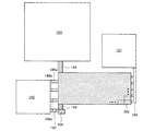
図2にブロック図を示す。図2の半導体装置は、フォトダイオード103、参照側のTFT104及び出力側のTFT105を有するカレントミラー回路111、高電圧電位(VDD)接続用電極(「高電位電極」ともいう)141、低電圧電位(VSS)接続用電極(「低電位電極」ともいう)142、フォトダイオード103並びにTFT104及び105を電気的に接続する配線144、TFT104及び105並びに電極141を電気的に接続する配線145、TFT104及び105並びに電極142を電気的に接続する配線146(配線146a、配線146b、配線146c、配線146d、等)を有している。なお図2において配線146は4本(配線146a、配線146b、配線146c、配線146d)しか示されていないが、必要に応じて本数は決めればよい。また出力側のTFT105は、複数のTFTによって形成されており、その数に応じて出力電流(光電流)が増幅される。
FIG. 2 shows a block diagram. 2 includes a
また図26に示すように、参照側のTFT104は、出力側のTFT105とは別に形成されていてもよい。その場合は配線146とは別配線147を介して、電極142に電気的に接続すればよい。
As shown in FIG. 26, the
参照側のTFT104は、電極142から近いところに配置され、配線抵抗等によってゲート電極にかかる電圧Vgateが下がらないようにする。
The
参照側のTFT104は、出力側のTFT105よりも電極142に近いところに配置する。参照側のTFT104と電極142とを電気的に接続する配線の長さは、出力側のTFT105と電極142とを電気的に接続する配線の長さよりも短い。参照側のTFT104と電極142との間の電流経路の長さは、出力側のTFT105と電極142との間の電流経路の長さよりも短い。これによりゲート電極にかかる電圧Vgateの低減を抑制することができる。
The reference-
参照側TFT104に寄生抵抗が発生してしまうと、TFT104のゲート電極にかかる電圧Vgateが、ゲート−ソース間電圧Vgsから寄生抵抗の抵抗値R×出力電流(光電流)I(=ΔV)の分だけ下がってしまう。
When parasitic resistance occurs in the
図4はTFT104のゲート電極にかかる電圧Vgateと出力電流(光電流)Iの関係を表す図であり、横軸は電圧Vgate(リニアスケール)、縦軸は光電流I(ログスケール)である。また図5は照度Eと出力電流(光電流)Iの関係を表しており、横軸は照度E(ログスケール)、縦軸は光電流I(ログスケール)である。
FIG. 4 is a diagram showing the relationship between the voltage V gate applied to the gate electrode of the
図4に示すように、寄生抵抗が発生しまうと、VgateがV1(寄生抵抗が最小のときのVgate)からV2(V1−ΔV:寄生抵抗が発生したときのVgate)となってしまう。光電流Iは、V1の時はI1で飽和するが、V2の時はI2で飽和していまい、それ以上流れなくなってしまう。図5に示すように光電流Iは光強度Eと比例するので、光電流IがI2で飽和してしまうと、感知できる最大光強度EはL2までとなってしまい、光電変換装置の感度が低下してしまう。 As shown in FIG. 4, when parasitic resistance occurs, V gate is changed from V 1 (V gate when the parasitic resistance is minimum) to V 2 (V 1 −ΔV: V gate when the parasitic resistance is generated). turn into. The photocurrent I saturates at I 1 when V 1 , but saturates at I 2 when V 2 , and stops flowing any more. Since the photocurrent I is proportional to the light intensity E as shown in FIG. 5, if the photocurrent I is saturated at I 2 , the maximum light intensity E that can be sensed is L 2 , and the photoelectric conversion device Sensitivity will decrease.
ただし実際には配線抵抗等の寄生抵抗を0にすることは難しいので、V1は寄生抵抗が発生しないときのVgateと必ずしも一致しないこともある。 However, in practice, it is difficult to set the parasitic resistance such as the wiring resistance to 0, and thus V 1 may not necessarily match V gate when the parasitic resistance is not generated.
しかしながら本発明では、参照側のTFT104は低電位電圧Vss用接続電極142に近いところに配置されるので、TFT104と電極142の間の配線抵抗は極小とすることができ、寄生抵抗の発生を最小限に防ぐことができる。これにより光電変換装置の感度の低下を抑制することができる。
However, in the present invention, the
またさらに配線抵抗を下げるためには、TFT104と電極142を電気的に接続する配線の幅を広げたり、配線を形成する導電膜の膜厚を増やせばよい。
In order to further reduce the wiring resistance, the width of the wiring that electrically connects the
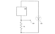
ところで、一般に信号処理が行い易いといわれている、出力信号形式を電圧として取り出す方法としては、負荷抵抗RLによって電流を電圧に変換する方法がある。具体的には、図6に示すように、フォトダイオード103とカレントミラー回路111を含む回路123、電源101、出力端子124、負荷抵抗RLを有する回路において、負荷抵抗RLを用いて出力電流を電圧に変換し、出力端子124にて電圧として外部に出力信号を取り出すことが可能となる。図1のカレントミラー回路111を含む回路123を図6の回路に組み込んだ回路について以下に説明する。
By the way, as a method of extracting an output signal format as a voltage, which is generally said to be easy to perform signal processing, there is a method of converting a current into a voltage by a load resistor RL . Specifically, as shown in FIG. 6, in a circuit having a
図1では、カレントミラー回路111を構成するTFT104のゲート電極は、カレントミラー回路111を構成するもう1つのTFT105のゲート電極に電気的に接続され、更にTFT104のドレイン電極(「ドレイン端子」ともいう)に電気的に接続されている。
In FIG. 1, the gate electrode of the
TFT104のドレイン端子は、フォトダイオード103を介してTFT105のドレイン端子に電気的に接続されている。
The drain terminal of the
TFT104のソース電極(「ソース端子」ともいう)は、TFT105のソース端子に電気的に接続されている。
A source electrode (also referred to as “source terminal”) of the
本実施の形態では、カレントミラー回路111を含む回路123の出力端子124は負荷抵抗RLを介して、電源101の低電位側へ電気的に接続される。
In the present embodiment, the
図1では、カレントミラー回路111を構成するTFT105のゲート電極は、TFT104のドレイン端子に電気的に接続されている。
In FIG. 1, the gate electrode of the
また、TFT104及び105のゲート電極は互いに接続されているので共通の電位が印加される。
Further, since the gate electrodes of the
図1では2個のTFTによる、カレントミラー回路の例を図示している。この時、104と105が同一の特性を有する場合、参照電流と出力電流の比は、1:1の関係となる。 FIG. 1 illustrates an example of a current mirror circuit using two TFTs. At this time, when 104 and 105 have the same characteristics, the ratio of the reference current and the output current is 1: 1.
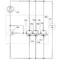
出力値をn倍とするための回路構成を図7及び図8に示す。図7の回路構成は、図1のTFT105をn個にしたものに相当する。図7に示すようにnチャネル型TFT104とnチャネル型TFT105の比を1:nにすることで、出力値をn倍とすることが可能となる。これは、TFTのチャネル幅Wを増加させ、TFTに流すことのできる電流の許容量をn倍とすることと同様の原理である。
7 and 8 show circuit configurations for increasing the output value by n times. The circuit configuration in FIG. 7 corresponds to the
例えば、出力値を100倍に設計する場合、nチャネルTFT104を1個、nチャネル型TFT105を100個並列接続することで、目標とした電流を得ることが可能となる。
For example, when designing the output value to be 100 times, a target current can be obtained by connecting one n-
図7中の回路118i(回路118a、回路118b、等)の詳細な回路構成を図8に示す。
FIG. 8 shows a detailed circuit configuration of the
図8の回路構成は、図1及び図7の回路構成を基にしており、同じ素子は同じ符号で表されている。すなわち、TFT105iのゲート電極は、端子119iに電気的に接続されており、またドレイン端子は端子120iに電気的に接続されている。またTFT105iのソース端子は、端子121iに電気的に接続されている。
The circuit configuration of FIG. 8 is based on the circuit configurations of FIGS. 1 and 7, and the same elements are denoted by the same reference numerals. That is, the gate electrode of the
なお図7中の回路118a、回路118b、等を、説明するために、そのうちの1つである回路118iを図8に示している。回路118iは図1の回路構成を基にしているので、図8の符号において「i」の付いている符号は、図1の「i」の付いていない符号と同じものである。すなわち、例えば図1のTFT105と図8のTFT105iは同じものである。
In order to describe the
したがって図7においては、nチャネル型TFT105は、n個のnチャネル型TFT105a、105b、105i、等から構成されていることとなる。これによりTFT104に流れる電流がn倍に増幅されて出力される。
Accordingly, in FIG. 7, the n-
尚、図7及び図8において図1と同じものを指示している場合は、同じ符号で示してある。 7 and 8, the same reference numerals are used to indicate the same components as those in FIG.
また、図1はカレントミラー回路111を、nチャネル型TFTを用いた等価回路として図示したものであるが、このnチャネル型TFTに代えてpチャネル型TFTを用いてもよい。
1 shows the
増幅回路をpチャネル型TFTで形成する場合は、図9に示す等価回路となる。図9に示すように、カレントミラー回路203はpチャネル型TFT201及び202を有している。pチャネル型TFT201は、pチャネル型TFT202よりも高電位電極141と近いところに配置される。pチャネル型TFT201と電極141との電気的接続配線の長さは、pチャネル型TFT202と電極141との電気的接続配線の長さよりも短い。pチャネル型TFT201と電極141との間の電流経路の長さは、pチャネル型TFT202と電極141との間の電流経路の長さよりも短い。なお図1と図9で同じものは同じ符号で示している。また出力信号形式を電圧として取り出すには、図6の回路123に代えて回路204を用いた構成にすればよい。
When the amplifier circuit is formed of a p-channel TFT, an equivalent circuit shown in FIG. 9 is obtained. As shown in FIG. 9, the
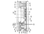
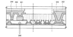
図1のTFT104及び105を含むカレントミラー回路111及びフォトダイオード103を含む回路123の断面図を図10に示す。
FIG. 10 shows a cross-sectional view of the
図10において、210は基板、212は下地絶縁膜、213はゲート絶縁膜である。 In FIG. 10, 210 is a substrate, 212 is a base insulating film, and 213 is a gate insulating film.
また、接続電極285、端子電極281、TFT104のソース電極またはドレイン電極282、及びTFT105のソース電極またはドレイン電極283は、高融点金属膜と低抵抗金属膜(アルミニウム合金または純アルミニウムなど)との積層構造となっている。ここでは、接続電極285、端子電極281、ソース電極またはドレイン電極282及び283は、チタン膜(Ti膜)とアルミニウム膜(Al膜)とTi膜とを順に積み重ねた三層構造とする。
The
また、高融点金属膜と低抵抗金属膜との積層構造の代わりに、単層の導電膜により形成することもできる。このような単層の導電膜として、チタン(Ti)、タングステン(W)、タンタル(Ta)、モリブデン(Mo)、ネオジウム(Nd)、コバルト(Co)、ジルコニウム(Zr)、亜鉛(Zn)、ルテニウム(Ru)、ロジウム(Rh)、パラジウム(Pd)、オスミウム(Os)、イリジウム(Ir)、白金(Pt)から選ばれた元素、または前記元素を主成分とする合金材料若しくは化合物材料からなる単層膜、或いは、これらの窒化物、例えば、窒化チタン、窒化タングステン、窒化タンタル、窒化モリブデンからなる単層膜を用いることができる。 Further, instead of the laminated structure of the refractory metal film and the low resistance metal film, a single-layer conductive film can be used. As such a single-layer conductive film, titanium (Ti), tungsten (W), tantalum (Ta), molybdenum (Mo), neodymium (Nd), cobalt (Co), zirconium (Zr), zinc (Zn), An element selected from ruthenium (Ru), rhodium (Rh), palladium (Pd), osmium (Os), iridium (Ir), platinum (Pt), or an alloy material or a compound material containing the element as a main component A single-layer film or a single-layer film made of these nitrides, for example, titanium nitride, tungsten nitride, tantalum nitride, or molybdenum nitride can be used.
また図10においては、nチャネル型TFT104及び105は1つのチャネル形成領域を含む構造(本明細書では「シングルゲート構造」という)のトップゲート型TFTの例を示しているが、チャネル形成領域が複数ある構造にしてオン電流値のバラツキを低減させてもよい。
In FIG. 10, n-
また、オフ電流値を低減するため、nチャネル型TFT104及び105に低濃度ドレイン(Lightly Doped Drain(LDD))領域を設けてもよい。LDD領域とは、チャネル形成領域と、高濃度に不純物元素を添加して形成するソース領域またはドレイン領域との間に低濃度に不純物元素を添加した領域のことであり、LDD領域を設けると、ドレイン領域近傍の電界を緩和してホットキャリア注入によるTFTの劣化を防ぐという効果がある。
Further, in order to reduce the off-current value, a lightly doped drain (LDD) region may be provided in the n-
また、ホットキャリアによるオン電流値の低下を防ぐため、nチャネル型TFT104及び105を、ゲート絶縁膜を介してLDD領域をゲート電極と重ねて配置させた構造(本明細書では「GOLD(Gate−drain Overlapped LDD)構造」と呼ぶ)としてもよい。
In order to prevent a decrease in the on-current value due to hot carriers, the n-
GOLD構造を用いた場合、LDD領域をゲート電極と重ねて形成しなかった場合よりも、さらにドレイン領域近傍の電界を緩和してホットキャリア注入によるTFTの劣化を防ぐ効果がある。このようなGOLD構造とすることで、ドレイン領域近傍の電界強度が緩和されてホットキャリア注入を防ぎ、TFTの劣化防止に有効である。 When the GOLD structure is used, there is an effect that the electric field in the vicinity of the drain region is further relaxed and TFT deterioration due to hot carrier injection is prevented, compared with the case where the LDD region is not formed overlapping the gate electrode. With such a GOLD structure, the electric field strength in the vicinity of the drain region is relaxed, hot carrier injection is prevented, and TFT deterioration is effective.
またカレントミラー回路111を形成するTFT104及び105は、トップゲート型TFTだけでなく、ボトムゲート型TFT、例えば逆スタガ型TFTでもよい。
The
また、配線215はTFT104のドレイン配線(ドレイン電極とも呼ぶ)またはソース配線(ソース電極とも呼ぶ)と電気的に接続している。また、216及び217は絶縁膜、285は接続電極である。なお、絶縁膜217は、CVD法により形成される酸化珪素膜を用いることが好ましい。絶縁膜217をCVD法で形成する酸化珪素膜とすると固着強度が向上する。
The
また、端子電極250は、配線215と同一工程で形成され、端子電極281は接続電極285と同一工程で形成されている。
The
また、端子電極221は、半田264で基板260の電極261に実装されている。また、端子電極222は端子電極221と同一工程で形成され、半田263で基板260の電極262に実装されている。
The
以下に、図10に示す、フォトダイオード103、並びにTFT104及び105を有するカレントミラー回路111を含む半導体装置を作製する工程について、図10、図11(A)〜図11(C)、図12(A)〜図12(C)、図13(A)〜図13(B)を用いて説明する。
In the following, a process for manufacturing a semiconductor device including the
まず、基板(第1の基板210)上に素子を形成する。ここでは基板210として、ガラス基板の一つであるAN100を用いる。
First, an element is formed over a substrate (first substrate 210). Here, AN100 which is one of glass substrates is used as the
次いで、プラズマCVD法で下地絶縁膜212となる窒素を含む酸化珪素膜(膜厚100nm)を形成し、さらに大気にふれることなく、半導体膜例えば水素を含む非晶質珪素膜(膜厚54nm)を積層形成する。また、下地絶縁膜212は酸化珪素膜、窒化珪素膜、窒素を含む酸化珪素膜を用いて積層してもよい。例えば、下地絶縁膜212として、酸素を含む窒化珪素膜を50nm、さらに窒素を含む酸化珪素膜を100nm積層した膜を形成してもよい。なお、窒素を含む酸化珪素膜や酸素を含む窒化珪素膜は、ガラス基板からのアルカリ金属などの不純物拡散を防止するブロッキング層として機能する。
Next, a silicon oxide film (thickness: 100 nm) containing nitrogen is formed as a
次いで、上記非晶質珪素膜を固相成長法、レーザ結晶化方法、触媒金属を用いた結晶化方法などにより結晶化させて、結晶構造を有する半導体膜(結晶性半導体膜)、例えば多結晶珪素膜を形成する。ここでは、触媒元素を用いた結晶化方法を用いて多結晶珪素膜を得る。重量換算で10ppmのニッケルを含む溶液をスピナーを用いて非晶質珪素膜表面に添加する。なお、スピナーで添加する方法に代えてスパッタ法でニッケル元素を全面に散布する方法を用いてもよい。次いで、加熱処理を行い結晶化させて結晶構造を有する半導体膜(ここでは多結晶珪素膜)を形成する。ここでは熱処理(500℃、1時間)の後、結晶化のための熱処理(550℃、4時間)を行って多結晶珪素膜を得る。 Next, the amorphous silicon film is crystallized by a solid phase growth method, a laser crystallization method, a crystallization method using a catalytic metal, or the like, so that a semiconductor film having a crystal structure (crystalline semiconductor film), for example, polycrystalline A silicon film is formed. Here, a polycrystalline silicon film is obtained by a crystallization method using a catalytic element. A solution containing 10 ppm of nickel in terms of weight is added to the surface of the amorphous silicon film using a spinner. Instead of adding with a spinner, a method of spreading nickel element over the entire surface by sputtering may be used. Next, heat treatment is performed for crystallization to form a semiconductor film having a crystal structure (here, a polycrystalline silicon film). Here, after heat treatment (500 ° C., 1 hour), heat treatment for crystallization (550 ° C., 4 hours) is performed to obtain a polycrystalline silicon film.
次いで、多結晶珪素膜表面の酸化膜を希フッ酸等で除去する。その後、結晶化率を高め、結晶粒内に残される欠陥を補修するためのレーザビームの照射を行う。 Next, the oxide film on the surface of the polycrystalline silicon film is removed with dilute hydrofluoric acid or the like. Thereafter, laser beam irradiation is performed to increase the crystallization rate and repair defects remaining in the crystal grains.
なお、非晶質珪素膜をレーザ結晶化方法で結晶化して結晶性半導体膜を得る場合、もしくは結晶構造を有する半導体膜を得た後結晶粒内に残される欠陥を補修するためにレーザ照射を行う場合には、以下に述べるレーザ照射方法で行えばよい。 Note that when an amorphous silicon film is crystallized by a laser crystallization method to obtain a crystalline semiconductor film, or after obtaining a semiconductor film having a crystal structure, laser irradiation is performed to repair defects remaining in crystal grains. When performing, the laser irradiation method described below may be used.
レーザ照射は、連続発振型のレーザビーム(CWレーザビーム)やパルス発振型のレーザビーム(パルスレーザビーム)を用いて行うことができる。ここで用いることができるレーザビームは、Arレーザ、Krレーザ、エキシマレーザなどの気体レーザ、単結晶のYAG、YVO4、フォルステライト(Mg2SiO4)、YAlO3、GdVO4、若しくは多結晶(セラミック)のYAG、Y2O3、YVO4、YAlO3、GdVO4に、ドーパントとしてNd、Yb、Cr、Ti、Ho、Er、Tm、Taのうち1種または複数種添加されているものを媒質とするレーザ、ガラスレーザ、ルビーレーザ、アレキサンドライトレーザ、Ti:サファイアレーザ、銅蒸気レーザまたは金蒸気レーザのうち一種または複数種から発振されるものを用いることができる。このようなレーザビームの基本波、及びこれらの基本波の第2高調波から第4高調波のレーザビームを照射することで、大粒径の結晶を得ることができる。例えば、Nd:YVO4レーザ(基本波1064nm)の第2高調波(532nm)や第3高調波(355nm)を用いることができる。このときレーザのエネルギー密度は0.01〜100MW/cm2程度(好ましくは0.1〜10MW/cm2)が必要である。そして、走査速度を10〜2000cm/sec程度として照射する。 Laser irradiation can be performed using a continuous wave laser beam (CW laser beam) or a pulsed laser beam (pulse laser beam). The laser beam that can be used here is a gas laser such as an Ar laser, a Kr laser, or an excimer laser, single crystal YAG, YVO 4 , forsterite (Mg 2 SiO 4 ), YAlO 3 , GdVO 4 , or polycrystalline ( (Ceramics) YAG, Y 2 O 3 , YVO 4 , YAlO 3 , GdVO 4 with one or more of Nd, Yb, Cr, Ti, Ho, Er, Tm, Ta added as dopants A laser oscillated from one or more of laser, glass laser, ruby laser, alexandrite laser, Ti: sapphire laser, copper vapor laser, or gold vapor laser as a medium can be used. By irradiating the fundamental wave of such a laser beam and the second to fourth harmonic laser beams of these fundamental waves, a crystal having a large grain size can be obtained. For example, a second harmonic (532 nm) or a third harmonic (355 nm) of an Nd: YVO 4 laser (fundamental wave 1064 nm) can be used. Energy density of the laser is about 0.01 to 100 MW / cm 2 (preferably 0.1 to 10 MW / cm 2) is required. Then, irradiation is performed at a scanning speed of about 10 to 2000 cm / sec.
なお、単結晶のYAG、YVO4、フォルステライト(Mg2SiO4)、YAlO3、GdVO4、若しくは多結晶(セラミック)のYAG、Y2O3、YVO4、YAlO3、GdVO4に、ドーパントとしてNd、Yb、Cr、Ti、Ho、Er、Tm、Taのうち1種または複数種添加されているものを媒質とするレーザ、Arレーザ、Krレーザ、またはTi:サファイアレーザは、連続発振をさせることが可能であり、Qスイッチ動作やモード同期などを行うことによって10MHz以上の発振周波数でパルス発振をさせることも可能である。10MHz以上の発振周波数でレーザビームを発振させると、半導体膜がレーザによって溶融してから固化するまでの間に、次のパルスが半導体膜に照射される。従って、発振周波数が低いパルスレーザを用いる場合と異なり、半導体膜中において固液界面を連続的に移動させることができるため、走査方向に向かって連続的に成長した結晶粒を得ることができる。 Note that single crystal YAG, YVO 4 , forsterite (Mg 2 SiO 4 ), YAlO 3 , GdVO 4 , or polycrystalline (ceramic) YAG, Y 2 O 3 , YVO 4 , YAlO 3 , GdVO 4 , dopants Nd, Yb, Cr, Ti, Ho, Er, Tm, and Ta, a laser that uses one or a plurality of types added as a medium, Ar laser, Kr laser, or Ti: sapphire laser It is also possible to oscillate pulses at an oscillation frequency of 10 MHz or more by performing Q switch operation or mode synchronization. When the laser beam is oscillated at an oscillation frequency of 10 MHz or more, the semiconductor film is irradiated with the next pulse during the period from when the semiconductor film is melted by the laser to solidification. Therefore, unlike the case of using a pulse laser having a low oscillation frequency, the solid-liquid interface can be continuously moved in the semiconductor film, so that crystal grains continuously grown in the scanning direction can be obtained.
媒質としてセラミック(多結晶)を用いると、短時間かつ低コストで自由な形状に媒質を形成することが可能である。単結晶を用いる場合、通常、直径数mm、長さ数十mmの円柱状の媒質が用いられているが、セラミックを用いる場合はさらに大きいものを作ることが可能である。 When ceramic (polycrystal) is used as the medium, it is possible to form the medium in a free shape in a short time and at low cost. When a single crystal is used, a cylindrical medium having a diameter of several millimeters and a length of several tens of millimeters is usually used. However, when ceramic is used, a larger one can be made.
発光に直接寄与する媒質中のNd、Ybなどのドーパントの濃度は、単結晶中でも多結晶中でも大きくは変えられないため、濃度を増加させることによるレーザの出力向上にはある程度限界がある。しかしながら、セラミックの場合、単結晶と比較して媒質の大きさを著しく大きくすることができるため大幅に出力が向上する。 Since the concentration of dopants such as Nd and Yb in the medium that directly contributes to light emission cannot be changed greatly regardless of whether it is a single crystal or a polycrystal, there is a certain limit to improving the laser output by increasing the concentration. However, in the case of ceramic, since the size of the medium can be remarkably increased as compared with the single crystal, the output is greatly improved.
さらに、セラミックの場合では、平行六面体形状や直方体形状の媒質を容易に形成することが可能である。このような形状の媒質を用いて、発振光を媒質の内部でジグザグに進行させると、発振光路を長くとることができる。そのため、増幅が大きくなり、大出力で発振させることが可能になる。また、このような形状の媒質から射出されるレーザビームは射出時の断面形状が四角形状であるため、丸状のビームと比較すると、線状ビームに整形するのに有利である。このように射出されたレーザビームを、光学系を用いて整形することによって、短辺の長さ1mm以下、長辺の長さ数mm〜数mの線状ビームを容易に得ることが可能となる。また、励起光を媒質に均一に照射することにより、線状ビームは長辺方向にエネルギー分布の均一なものとなる。 Further, in the case of ceramic, a medium having a parallelepiped shape or a rectangular parallelepiped shape can be easily formed. When a medium having such a shape is used to cause oscillation light to travel in a zigzag manner inside the medium, the oscillation optical path can be made longer. As a result, amplification is increased and oscillation can be performed with high output. Further, since the laser beam emitted from the medium having such a shape has a quadrangular cross-sectional shape at the time of emission, it is advantageous for shaping into a linear beam as compared with a round beam. By shaping the emitted laser beam using an optical system, it is possible to easily obtain a linear beam having a short side length of 1 mm or less and a long side length of several mm to several m. Become. In addition, by irradiating the medium with the excitation light uniformly, the linear beam has a uniform energy distribution in the long side direction.
この線状ビームを半導体膜に照射することによって、半導体膜の全面をより均一にアニールすることが可能になる。線状ビームの両端まで均一なアニールが必要な場合は、スリットを用いてエネルギーの減衰部を遮光するなどの工夫が必要となる。 By irradiating the semiconductor film with this linear beam, the entire surface of the semiconductor film can be annealed more uniformly. When uniform annealing is required up to both ends of the linear beam, it is necessary to devise measures such as shielding the energy attenuation portion using a slit.
なお、レーザ照射を大気中、または酸素雰囲気中で行う場合は、レーザビームの照射により表面に酸化膜が形成される。 Note that in the case where laser irradiation is performed in the air or an oxygen atmosphere, an oxide film is formed on the surface by laser beam irradiation.
次いで、上記レーザビームの照射により形成された酸化膜に加え、オゾン水で表面を120秒処理して合計1〜5nmの酸化膜からなるバリア層を形成する。このバリア層は、結晶化させるために添加した触媒元素、例えばニッケル(Ni)を膜中から除去するために形成する。ここではオゾン水を用いてバリア層を形成したが、酸素雰囲気下の紫外線の照射で結晶構造を有する半導体膜の表面を酸化する方法や酸素プラズマ処理により結晶構造を有する半導体膜の表面を酸化する方法やプラズマCVD法やスパッタ法や蒸着法などで1〜10nm程度の酸化膜を堆積してバリア層を形成してもよい。また、バリア層を形成する前にレーザビームの照射により形成された酸化膜を除去してもよい。 Next, in addition to the oxide film formed by the laser beam irradiation, the surface is treated with ozone water for 120 seconds to form a barrier layer made of an oxide film having a total thickness of 1 to 5 nm. This barrier layer is formed to remove a catalyst element added for crystallization, for example, nickel (Ni) from the film. Here, the barrier layer is formed using ozone water, but the surface of the semiconductor film having a crystal structure is oxidized by a method of oxidizing the surface of the semiconductor film having a crystal structure by irradiation with ultraviolet light in an oxygen atmosphere or the oxygen plasma treatment. The barrier layer may be formed by depositing an oxide film of about 1 to 10 nm by a method, plasma CVD method, sputtering method or vapor deposition method. Further, the oxide film formed by laser beam irradiation may be removed before forming the barrier layer.
次いで、バリア層上にスパッタ法にてゲッタリングサイトとなるアルゴン元素を含む非晶質珪素膜を10nm〜400nm、ここでは膜厚100nmで成膜する。ここでは、アルゴン元素を含む非晶質珪素膜は、シリコンターゲットを用いてアルゴンを含む雰囲気下で形成する。プラズマCVD法を用いてアルゴン元素を含む非晶質珪素膜を形成する場合、成膜条件は、モノシランとアルゴンの流量比(SiH4:Ar)を1:99とし、成膜圧力を6.665Paとし、RFパワー密度を0.087W/cm2とし、成膜温度を350℃とする。 Next, an amorphous silicon film containing an argon element serving as a gettering site is formed with a thickness of 10 to 400 nm, here 100 nm, over the barrier layer by a sputtering method. Here, the amorphous silicon film containing an argon element is formed using a silicon target in an atmosphere containing argon. In the case where an amorphous silicon film containing an argon element is formed using a plasma CVD method, the film formation conditions are as follows: the flow ratio of monosilane to argon (SiH 4 : Ar) is 1:99, and the film formation pressure is 6.665 Pa. The RF power density is 0.087 W / cm 2 and the film formation temperature is 350 ° C.
その後、650℃に加熱された炉に入れて3分の熱処理を行い触媒元素を除去(ゲッタリング)する。これにより結晶構造を有する半導体膜中の触媒元素濃度が低減される。炉に代えてランプアニール装置を用いてもよい。 Thereafter, the catalyst element is removed (gettering) by performing a heat treatment for 3 minutes in a furnace heated to 650 ° C. As a result, the concentration of the catalytic element in the semiconductor film having a crystal structure is reduced. A lamp annealing apparatus may be used instead of the furnace.
次いで、バリア層をエッチングストッパとして、ゲッタリングサイトであるアルゴン元素を含む非晶質珪素膜を選択的に除去した後、バリア層を希フッ酸で選択的に除去する。なお、ゲッタリングの際、ニッケルは酸素濃度の高い領域に移動しやすい傾向があるため、酸化膜からなるバリア層をゲッタリング後に除去することが望ましい。 Next, the amorphous silicon film containing an argon element which is a gettering site is selectively removed using the barrier layer as an etching stopper, and then the barrier layer is selectively removed with dilute hydrofluoric acid. Note that during gettering, nickel tends to move to a region with a high oxygen concentration, and thus it is desirable to remove the barrier layer made of an oxide film after gettering.
なお、触媒元素を用いて半導体膜の結晶化を行わない場合には、上述したバリア層の形成、ゲッタリングサイトの形成、ゲッタリングのための熱処理、ゲッタリングサイトの除去、バリア層の除去などの工程は不要である。 Note that in the case where the semiconductor film is not crystallized using a catalytic element, the above-described barrier layer formation, gettering site formation, heat treatment for gettering, gettering site removal, barrier layer removal, etc. This step is unnecessary.
次いで、得られた結晶構造を有する半導体膜(例えば結晶性珪素膜)の表面にオゾン水で薄い酸化膜を形成した後、第1のフォトマスクを用いてレジストからなるマスクを形成し、所望の形状にエッチング処理して島状に分離された半導体膜(本明細書では「島状半導体領域」という)231及び232を形成する(図11(A)参照)。島状半導体領域を形成した後、レジストからなるマスクを除去する。 Next, after forming a thin oxide film with ozone water on the surface of the obtained semiconductor film having a crystalline structure (for example, a crystalline silicon film), a mask made of resist is formed using a first photomask, and a desired film is formed. Semiconductor films (referred to as “island semiconductor regions” in this specification) 231 and 232 separated into island shapes are formed by etching into a shape (see FIG. 11A). After the island-shaped semiconductor region is formed, the resist mask is removed.
次いで、必要があればTFTのしきい値電圧を制御するために微量な不純物元素(ホウ素またはリン)のドーピングを行う。ここでは、ジボラン(B2H6)を質量分離しないでプラズマ励起したイオンドープ法を用いる。 Next, if necessary, a small amount of impurity element (boron or phosphorus) is doped in order to control the threshold voltage of the TFT. Here, an ion doping method in which diborane (B 2 H 6 ) is plasma-excited without mass separation is used.
次いで、フッ酸を含むエッチャントで酸化膜を除去すると同時に島状半導体領域231及び232の表面を洗浄した後、ゲート絶縁膜213となる珪素を主成分とする絶縁膜を形成する。ここでは、プラズマCVD法により115nmの厚さで窒素を含む酸化珪素膜(組成比Si=32%、O=59%、N=7%、H=2%)で形成する。
Next, the oxide film is removed with an etchant containing hydrofluoric acid, and at the same time, the surfaces of the island-shaped
次いで、ゲート絶縁膜213上に金属膜を形成した後、ゲート電極234及び235、配線214及び215、端子電極250を形成する(図11(B)参照)。
Next, after a metal film is formed over the
また、ゲート電極234及び235、配線214及び215、端子電極250として、チタン(Ti)、タングステン(W)、タンタル(Ta)、モリブデン(Mo)、ネオジウム(Nd)、コバルト(Co)、ジルコニウム(Zr)、亜鉛(Zn)、ルテニウム(Ru)、ロジウム(Rh)、パラジウム(Pd)、オスミウム(Os)、イリジウム(Ir)、白金(Pt)、アルミニウム(Al)、金(Au)、銀(Ag)、銅(Cu)から選ばれた元素、または前記元素を主成分とする合金材料若しくは化合物材料からなる単層膜、或いは、これらの窒化物、例えば、窒化チタン、窒化タングステン、窒化タンタル、窒化モリブデンからなる単層膜を用いることができる。
Further, as the
また、上記の単層膜の代わりに積層膜を用いてもよい。例えば、ゲート電極234及び235、配線214及び215、端子電極250として、窒化タンタル及びタングステン(W)をそれぞれ30nm、370nm積層した膜を用いてもよい。
Further, a laminated film may be used instead of the single layer film. For example, as the
次いで、島状半導体領域231及び232への一導電型を付与する不純物の導入を行って、TFT105のソース領域またはドレイン領域237、及びTFT104のソース領域またはドレイン領域238の形成を行う。本実施の形態ではnチャネル型TFTを形成するので、n型の不純物、例えばリン(P)、砒素(As)を島状半導体領域231及び232に導入する(図11(C)参照)。
Next, an impurity imparting one conductivity type is introduced into the island-shaped
次いで、CVD法により酸化珪素膜を含む第1の層間絶縁膜(図示しない)を50nm形成した後、それぞれの島状半導体領域に添加された不純物元素を活性化処理する工程を行う。この活性化工程は、ランプ光源を用いたラピッドサーマルアニール法(RTA法)、或いはYAGレーザまたはエキシマレーザを裏面から照射する方法、或いは炉を用いた熱処理、或いはこれらの方法のうち、いずれかと組み合わせた方法によって行う。 Next, after forming a first interlayer insulating film (not shown) including a silicon oxide film by CVD with a thickness of 50 nm, a step of activating the impurity element added to each island-like semiconductor region is performed. This activation process is performed by a rapid thermal annealing method (RTA method) using a lamp light source, a method of irradiating a YAG laser or an excimer laser from the back surface, a heat treatment using a furnace, or a combination thereof. By different methods.
次いで、水素及び酸素を含む窒化珪素膜を含む第2の層間絶縁膜216を、例えば10nmの膜厚で形成する。
Next, a second
次いで、第2の層間絶縁膜216上に絶縁物材料から成る第3の層間絶縁膜217を形成する(図12(A)参照)。第3の層間絶縁膜217はCVD法で得られる絶縁膜を用いることができる。本実施の形態においては密着性を向上させるため、第3の層間絶縁膜217として、900nmの膜厚で形成した窒素を含む酸化珪素膜を形成する。
Next, a third
次に、熱処理(300〜550℃で1〜12時間の熱処理、例えば窒素雰囲気中410℃で1時間)を行い、島状半導体膜を水素化する。この工程は第2の層間絶縁膜216に含まれる水素により島状半導体膜のダングリングボンドを終端させるために行うものである。ゲート絶縁膜213の存在に関係なく島状半導体膜を水素化することができる。
Next, heat treatment (300 to 550 ° C. for 1 to 12 hours, for example, in a nitrogen atmosphere at 410 ° C. for 1 hour) is performed to hydrogenate the island-shaped semiconductor film. This step is performed in order to terminate dangling bonds of the island-shaped semiconductor film with hydrogen contained in the second
また第3の層間絶縁膜217として、シロキサンを用いた絶縁膜、及びそれらの積層構造を用いることも可能である。シロキサンは、シリコン(Si)と酸素(O)との結合で骨格構造で構成される。置換基として、少なくとも水素を含む有機基(例えばアルキル基、芳香族炭化水素)が用いられる。置換基として、フルオロ基を用いてもよい。または置換基として、少なくとも水素を含む有機基と、フルオロ基とを用いてもよい。
Further, as the third
第3の層間絶縁膜217としてシロキサンを用いた絶縁膜、及びそれらの積層構造を用いた場合は、第2の層間絶縁膜216を形成後、島状半導体膜を水素化するための熱処理を行い、次に第3の層間絶縁膜217を形成することもできる。
In the case where an insulating film using siloxane and a stacked structure thereof are used as the third
次いで、レジストからなるマスクを形成し、第1の層間絶縁膜、第2の層間絶縁膜216及び第3の層間絶縁膜217またはゲート絶縁膜213を選択的にエッチングしてコンタクトホールを形成する。そして、レジストからなるマスクを除去する。
Next, a resist mask is formed, and the first interlayer insulating film, the second
なお、第3の層間絶縁膜217は必要に応じて形成すればよく、第3の層間絶縁膜217を形成しない場合は、第2の層間絶縁膜216を形成後に第1の層間絶縁膜、第2の層間絶縁膜216及びゲート絶縁膜213を選択的にエッチングしてコンタクトホールを形成する。
Note that the third
次いで、スパッタ法で金属積層膜を成膜した後、レジストからなるマスクを形成し、選択的に金属膜をエッチングして、配線284、接続電極285、端子電極281、TFT104のソース電極またはドレイン電極282、TFT105のソース電極またはドレイン電極283を形成する(図12(B)参照)。
Next, after a metal laminated film is formed by sputtering, a mask made of a resist is formed, and the metal film is selectively etched to form a
図12(B)では、配線284、接続電極285、端子電極281、TFT104のソース電極またはドレイン電極282、及びTFT105のソース電極またはドレイン電極283を、単層の導電膜から形成している。
In FIG. 12B, the
このような単層として、耐熱性及び導電率等の点からチタン膜(Ti膜)が好ましい。またチタン膜に変えて、タングステン(W)、タンタル(Ta)、モリブデン(Mo)、ネオジウム(Nd)、コバルト(Co)、ジルコニウム(Zr)、亜鉛(Zn)、ルテニウム(Ru)、ロジウム(Rh)、パラジウム(Pd)、オスミウム(Os)、イリジウム(Ir)、白金(Pt)から選ばれた元素、または前記元素を主成分とする合金材料若しくは化合物材料からなる単層膜、或いは、これらの窒化物、例えば、窒化チタン、窒化タングステン、窒化タンタル、窒化モリブデンからなる単層膜を用いることができる。配線284、接続電極285、端子電極281、及びTFT104のソース電極またはドレイン電極282、及びTFT105のソース電極またはドレイン電極283を単層膜にすることにより、作製工程において成膜回数を減少させることが可能となる。
As such a single layer, a titanium film (Ti film) is preferable from the viewpoints of heat resistance and electrical conductivity. Further, in place of the titanium film, tungsten (W), tantalum (Ta), molybdenum (Mo), neodymium (Nd), cobalt (Co), zirconium (Zr), zinc (Zn), ruthenium (Ru), rhodium (Rh) ), Palladium (Pd), osmium (Os), iridium (Ir), platinum (Pt), or a single layer film made of an alloy material or a compound material containing the element as a main component, or these A single layer film made of a nitride such as titanium nitride, tungsten nitride, tantalum nitride, or molybdenum nitride can be used. By forming the
また、配線219、接続電極220、端子電極251、TFT104のソース電極またはドレイン電極241、及びTFT105のソース電極またはドレイン電極242に保護電極を設けた場合について図12(C)に示す。
FIG. 12C illustrates the case where a protective electrode is provided for the
まず配線219、接続電極220、端子電極251、TFT104のソース電極またはドレイン電極241、及びTFT105のソース電極またはドレイン電極242のそれぞれの下層導電膜は、高融点金属膜と低抵抗金属膜(アルミニウム合金または純アルミニウムなど)との積層構造となっている。ここでは、配線219、接続電極220、端子電極251、ソース電極またはドレイン電極241及び242の下層導電膜は、チタン膜(Ti膜)とアルミニウム膜(Al膜)とTi膜とを順に積み重ねた三層構造とする。
First, the lower conductive films of the
さらに配線219、接続電極220、端子電極251、TFT104のソース電極またはドレイン電極241、及びTFT105のソース電極またはドレイン電極242を覆うように、それぞれ保護電極218、保護電極245、保護電極248、保護電極246及び保護電極247が形成されている。
Further, a
後に形成される光電変換層103をエッチングする際に、配線219は、覆っている保護電極218によって保護される。保護電極218の材料は、光電変換層103をエッチングするガス(またはエッチャント)に対して光電変換層103よりもエッチング速度の小さい導電材料であることが好ましい。加えて、保護電極218の材料は、光電変換層103と反応して合金とならない導電材料であることが好ましい。なおその他の保護電極245、保護電極248、保護電極246及び保護電極247も保護電極218と同様の材料及び作製工程により形成される。
When the
例えば、後に形成される光電変換層(代表的にはアモルファスシリコン)と反応して合金になりにくい導電性の金属膜(チタン(Ti)またはモリブデン(Mo)など)を成膜した後、レジストからなるマスクを形成し、選択的に導電性の金属膜をエッチングして配線219を覆う保護電極218を形成する。ここではスパッタ法で得られる膜厚200nmのTi膜を用いる。なお、同様に接続電極220、端子電極251、TFT104のソース電極またはドレイン電極241、TFT105のソース電極またはドレイン電極242も導電性の金属膜で覆われ、それぞれ保護電極245、248、246、247が形成される。従って、導電性の金属膜は、これらの電極における2層目のAl膜が露呈されている側面も覆い、導電性の金属膜は光電変換層へのアルミニウム原子の拡散も防止できる。
For example, after forming a conductive metal film (such as titanium (Ti) or molybdenum (Mo)) that hardly reacts with a photoelectric conversion layer (typically amorphous silicon) that is formed later, A
次に第3の層間絶縁膜217上に、p型半導体層103p、i型半導体層103i及びn型半導体層103nを含む光電変換層103を形成する。
Next, the
p型半導体層103pは、13属の不純物元素、例えばホウ素(B)を含んだアモルファスシリコン膜をプラズマCVD法にて成膜して形成すればよい。
The p-
図13(A)では、配線284は光電変換層103の最下層、本実施の形態ではp型半導体層103pと接している。
In FIG. 13A, the
また保護電極を形成する場合は、配線219及び保護電極218は光電変換層103の最下層、本実施の形態ではp型半導体層103pと接することとなる。
In the case of forming a protective electrode, the
p型半導体層103pを形成したら、さらにi型半導体層103i及びn型半導体層103nを順に形成する。これによりp型半導体層103p、i型半導体層103i及びn型半導体層103nを有する光電変換層103が形成される。
After the p-
i型半導体層103iとしては、例えばプラズマCVD法でアモルファスシリコン膜を形成すればよい。またn型半導体層103nとしては、15属の不純物元素、例えばリン(P)を含むアモルファスシリコン膜を形成してもよいし、アモルファスシリコン膜を形成後、15属の不純物元素を導入してもよい。
As the i-
またp型半導体層103p、i型半導体層103i、n型半導体層103nとして、アモルファス半導体膜だけではなく、セミアモルファス半導体膜を用いてもよい。
Further, as the p-
次いで、全面に絶縁物材料(例えば珪素を含む無機絶縁膜)からなる封止層224を厚さ(1μm〜30μm)で形成して図13(A)の状態を得る。ここでは絶縁物材料膜としてCVD法により、膜厚1μmの窒素を含む酸化珪素膜を形成する。CVD法による絶縁膜を用いることによって密着性の向上を図っている。
Next, a
次いで、封止層224をエッチングして開口部を設けた後、スパッタ法により端子電極221及び222を形成する。端子電極221及び222は、チタン膜(Ti膜)(100nm)と、ニッケル膜(Ni)膜(300nm)と、金膜(Au膜)(50nm)との積層膜とする。こうして得られる端子電極221及び端子電極222の固着強度は5Nを超え、端子電極として十分な固着強度を有している。
Next, after the
以上の工程で、半田接続が可能な端子電極221及び端子電極222が形成され、図13(B)に示す構造が得られる。
Through the above steps, the
次いで、個々に切断して複数の光センサチップを切り出す。1枚の大面積基板(例えば600cm×720cm)からは大量の光センサチップ(2mm×1.5mm)を製造することが可能である。 Next, a plurality of optical sensor chips are cut out individually. A large amount of optical sensor chips (2 mm × 1.5 mm) can be manufactured from one large-area substrate (for example, 600 cm × 720 cm).
切り出した1つの光センサチップ(2mm×1.5mm)の断面図を図14(A)に示し、その下面図を図14(B)、上面図を図14(C)に示す。図14(A)〜図14(C)において、図10と同一である箇所には同じ符号を用いている。なお、図14(A)において、基板210と、素子形成領域291と、端子電極221及び端子電極222とを含む総膜厚は、0.8±0.05mmである。
A cross-sectional view of one cut out optical sensor chip (2 mm × 1.5 mm) is shown in FIG. 14A, a bottom view thereof is shown in FIG. 14B, and a top view thereof is shown in FIG. 14A to 14C, the same reference numerals are used for portions that are the same as those in FIG. In FIG. 14A, the total film thickness including the
また、光センサチップの総膜厚を薄くするために、基板210をCMP処理等によって削って薄くした後、ダイサーで個々に切断して複数の光センサチップを切り出してもよい。
In order to reduce the total film thickness of the optical sensor chip, the
また、図14(B)において、端子電極221及び222の一つの電極サイズは、0.6mm×1.1mmであり、電極間隔は0.4mmである。また、図14(C)において受光部292の面積は、1.57mm2である。また、増幅回路部293には、約100個のTFTが設けられている。
In FIG. 14B, one electrode size of the
最後に、得られた光センサチップを基板260の実装面に実装する。なお、端子電極221と電極261、並びに端子電極222と電極262との接続には、それぞれ半田264及び263を用い、予め基板260の電極261及び262上にスクリーン印刷法などによって半田ペーストを形成しておき、半田と端子電極を当接した状態にしてから半田リフロー処理を行って実装する。半田リフロー処理は、例えば不活性ガス雰囲気中、255℃〜265℃程度の温度で約10秒行う。また、半田の他に金属(金、銀等)で形成されるバンプ、または導電性樹脂で形成されるバンプ等を用いることができる。また、環境問題を考慮して鉛フリーはんだを用いて実装してもよい(図10参照)。
Finally, the obtained optical sensor chip is mounted on the mounting surface of the
以上のようにして、光電変換層103を含む光電変換装置、カレントミラー回路111を有する半導体装置を得ることが可能である。
As described above, a photoelectric conversion device including the
光200は、矢印に示すように基板210から入り、光電変換層103に到達する。
The light 200 enters from the
本実施の形態により、光感度の低減が抑制された光電変換装置を有する半導体装置を得ることができる。 According to this embodiment mode, a semiconductor device including a photoelectric conversion device in which reduction in photosensitivity is suppressed can be obtained.
なお本実施の形態は、必要であれば他の実施の形態と組み合わせてもよい。 Note that this embodiment may be combined with other embodiments if necessary.
[実施の形態2]
本実施の形態では、増幅回路をpチャネル型TFTで形成する例を、図9及び図15を用いて説明する。なお、実施の形態1と同じものは同じ符号で示しており、それぞれ実施の形態1に記載された作製工程に基づいて作成すればよい。
[Embodiment 2]
In this embodiment, an example in which an amplifier circuit is formed using a p-channel TFT will be described with reference to FIGS. Note that the same components as those in
増幅回路、例えばカレントミラー回路203をpチャネル型TFT201及び202で形成する場合には、実施の形態1の島状半導体領域への一導電型を付与する不純物を、p型の不純物、例えばホウ素(B)に代えればよい。
In the case where the amplifier circuit, for example, the
カレントミラー回路203をpチャネル型TFT201及び202で作成した場合の本実施の形態の光センサの等価回路図を図9、断面図を図15に示す。
FIG. 9 shows an equivalent circuit diagram of the photosensor of this embodiment and FIG. 15 shows a cross-sectional view when the
図9及び図15において、端子電極221は光電変換層103のn型半導体層103n及びpチャネル型TFT201に電気的に接続され、端子電極222はpチャネル型TFT202に電気的に接続されている。pチャネル型TFT201は、光電変換層103のアノード側の電極と電気的に接続される。光電変換層103は、pチャネル型TFT201と電気的に接続する第2の電極(アノード側の電極)上にn型半導体層103n、i型半導体層103i、p型半導体層103pを順次積層した後、第1の電極(カソード側の電極)を形成すればよい。
9 and 15, the
また、積層順序を逆にした光電変換層としてもよく、第1の電極(カソード側の電極)上にp型半導体層、i型半導体層、n型半導体層を順次積層した後、pチャネル型TFT201と電気的に接続する第2の電極(アノード側の電極)を形成してもよい。
Alternatively, a photoelectric conversion layer in which the stacking order is reversed may be used. After sequentially stacking a p-type semiconductor layer, an i-type semiconductor layer, and an n-type semiconductor layer on the first electrode (cathode side electrode), a p-channel type is formed. A second electrode (electrode on the anode side) that is electrically connected to the
光200は、矢印に示すように基板210から入り、光電変換層103に到達する。
The light 200 enters from the
図15に示すように、pチャネル型TFT201及び202の島状半導体領域には、p型の不純物、例えばホウ素(B)が導入されており、pチャネル型TFT201にはソース領域またはドレイン領域271、pチャネル型TFT202にはソース領域またはドレイン領域272が形成される。
As shown in FIG. 15, p-type impurities such as boron (B) are introduced into the island-shaped semiconductor regions of the p-
配線284、接続電極285、端子電極281、及びTFT201のソース電極またはドレイン電極283、及びTFT202のソース電極またはドレイン電極282は、実施の形態1の記載に従って、単層の導電膜を用いてそれぞれの配線や電極を形成される。
The
また図12(C)と同様に、配線284、接続電極285、端子電極281、及びTFT201のソース電極またはドレイン電極283、及びTFT202のソース電極またはドレイン電極282に代えて、配線219及びその保護電極218、接続電極220及びその保護電極245、端子電極251及びその保護電極248、TFT201のソース電極またはドレイン電極242及びその保護電極247、並びにTFT202のソース電極またはドレイン電極241及びその保護電極246を形成してもよい。それぞれの作製方法については、実施の形態1に基づくものである。
12C, instead of the
本実施の形態により、光感度の低減が抑制された光電変換装置を有する半導体装置を得ることができる。 According to this embodiment mode, a semiconductor device including a photoelectric conversion device in which reduction in photosensitivity is suppressed can be obtained.
なお本実施の形態は、必要であれば他の実施の形態と組み合わせてもよい。 Note that this embodiment may be combined with other embodiments if necessary.
[実施の形態3]
本実施の形態ではボトムゲート型TFTを用いて形成した増幅回路、光センサ及びその作製方法の例を、図16(A)〜図16(E)、図17(A)〜図17(D)、図18を用いて説明する。なお、実施の形態1〜実施の形態2と同じものは同じ符号で示している。
[Embodiment 3]
In this embodiment, an example of an amplifier circuit, an optical sensor, and a manufacturing method thereof, which are formed using bottom-gate TFTs, is described with reference to FIGS. 16 (A) to 16 (E) and FIGS. 17 (A) to 17 (D). This will be described with reference to FIG. In addition, the same thing as Embodiment 1- Embodiment 2 is shown with the same code | symbol.
まず基板210上に、下地絶縁膜212及び金属膜311を形成する(図16(A)参照)。この金属膜311として、本実施の形態では例えば窒化タンタル及びタングステン(W)をそれぞれ30nm、370nm積層した膜を用いる。
First, the
また、金属膜311として、上記以外にもチタン(Ti)、タングステン(W)、タンタル(Ta)、モリブデン(Mo)、ネオジウム(Nd)、コバルト(Co)、ジルコニウム(Zr)、亜鉛(Zn)、ルテニウム(Ru)、ロジウム(Rh)、パラジウム(Pd)、オスミウム(Os)、イリジウム(Ir)、白金(Pt)、アルミニウム(Al)、金(Au)、銀(Ag)、銅(Cu)から選ばれた元素、または前記元素を主成分とする合金材料若しくは化合物材料からなる単層膜、或いは、これらの窒化物、例えば、窒化チタン、窒化タングステン、窒化タンタル、窒化モリブデンからなる単層膜を用いることができる。
In addition to the above, as the
なお、下地絶縁膜212を基板210上に形成せず、金属膜311を直接基板210に形成してもよい。
Note that the
次に金属膜311を用いてゲート電極312及び313、配線214及び215、端子電極250を形成する(図16(B)参照)。
Next,
次いで、ゲート電極312及び313、配線214及び215、端子電極250を覆うゲート絶縁膜314を形成する。本実施の形態では、珪素を主成分とする絶縁膜、例えばプラズマCVD法により115nmの厚さで窒素を含む酸化珪素膜(組成比Si=32%、O=59%、N=7%、H=2%)を用いてゲート絶縁膜314を形成する。
Next, a
次にゲート絶縁膜314上に島状半導体領域315及び316を形成する。島状半導体領域315及び316は、実施の形態1で述べた島状半導体領域231及び232と同様の材料及び作製工程により形成すればよい(図16(C)参照)。
Next, island-shaped
島状半導体領域315及び316を形成したら、後にTFT301のソース領域またはドレイン領域321、及びTFT302のソース領域またはドレイン領域322となる領域以外を覆ってマスク318を形成し、一導電型を付与する不純物の導入を行う(図16(D)参照)。一導電型の不純物としては、nチャネル型TFTを形成する場合には、n型不純物としてリン(P)、砒素(As)を用い、pチャネル型TFTを形成する場合には、p型不純物としてホウ素(B)を用いればよい。本実施の形態ではn型不純物であるリン(P)を島状半導体領域315及び316に導入し、TFT301のソース領域またはドレイン領域321及びソース領域及びドレイン領域の間にチャネル形成領域、並びにTFT302のソース領域またはドレイン領域322、及びソース領域及びドレイン領域の間にチャネル形成領域を形成する。
After the island-shaped
次いでマスク318を除去し、図示しない第1の層間絶縁膜、第2の層間絶縁膜216及び第3の層間絶縁膜217を形成する(図16(E)参照)。第1の層間絶縁膜、第2の層間絶縁膜216及び第3の層間絶縁膜217の材料及び作製工程は実施の形態1の記載に基づけばよい。
Next, the
次に第1の層間絶縁膜、第2の層間絶縁膜216及び第3の層間絶縁膜217にコンタクトホールを形成し、単層の金属膜を成膜し、さらに選択的に金属膜をエッチングして、配線284、接続電極285、端子電極281、及びTFT301のソース電極またはドレイン電極341、及びTFT302のソース電極またはドレイン電極342が形成される(図17(A)参照)。
Next, contact holes are formed in the first interlayer insulating film, the second
また配線284、接続電極285、端子電極281、及びTFT301のソース電極またはドレイン電極341、及びTFT302のソース電極またはドレイン電極342を、単層の導電膜に代えて、積層膜によって形成してもよい。積層膜によってこれらを形成した例を図17(B)に示す。
In addition, the
図17(B)では、配線284、接続電極285、端子電極281、及びTFT301のソース電極またはドレイン電極341、及びTFT302のソース電極またはドレイン電極342に代えて、配線219及びその保護電極218、接続電極220及びその保護電極245、端子電極251及びその保護電極248、TFT301のソース電極またはドレイン電極331及びその保護電極336、並びにTFT302のソース電極またはドレイン電極332及びその保護電極337を形成する。
In FIG. 17B, instead of the
以上の工程で、ボトムゲート型TFT301及び302を作製することができる。ボトムゲート型TFT301及び302により、カレントミラー回路303を形成できる。
Through the above steps,
次に第3の層間絶縁膜217上に、p型半導体層103p、i型半導体層103i及びn型半導体層103nを含む光電変換層103を形成する(図17(C)参照)。光電変換層103の材料及び作製工程等は、実施の形態1〜実施の形態2を参照すればよい。
Next, the
次いで封止層224、端子電極221及び222を形成する(図17(D)参照)。端子電極221はn型半導体層100nに接続されており、端子電極222は端子電極221と同一工程で形成される。
Next, a
さらに電極261及び262を有する基板260を、半田263及び264で実装する。なお基板260上の電極261は、半田264で端子電極221に実装されている。また基板260の電極262は、半田263で端子電極222に実装されている(図18参照)。
Further, a
光200は、矢印に示すように基板210から入り、光電変換層103に到達する。
The light 200 enters from the
なお図17(B)の構成の半導体装置を用いても、上記の作製工程に従えば図18に示す半導体装置と同様な半導体装置を作製することができる。 Note that even when the semiconductor device having the structure illustrated in FIG. 17B is used, a semiconductor device similar to the semiconductor device illustrated in FIG. 18 can be manufactured according to the manufacturing steps described above.
本実施の形態により、光感度の低減が抑制された光電変換装置を有する半導体装置を得ることができる。 According to this embodiment mode, a semiconductor device including a photoelectric conversion device in which reduction in photosensitivity is suppressed can be obtained.
なお本実施の形態は、必要であれば他の実施の形態と組み合わせてもよい。 Note that this embodiment may be combined with other embodiments if necessary.
[実施の形態4]
本実施の形態では、電源として用いられるバッテリについて、図27、図28(A)〜図28(B)、図29(A)〜図29(E)、図30、図31、図32、図33用いて以下に説明する。
[Embodiment 4]
In this embodiment mode, a battery used as a power source is illustrated in FIGS. 27, 28A to 28B, 29A to 29E, FIG. 30, FIG. 31, FIG. 33 will be described below.
本明細書において、バッテリと、アンテナと、アンテナが受信した電磁波により生ずる起電力をバッテリに充電する回路と、該起電力を充電する媒体とを備えた装置をRFバッテリ又は無線電池とも呼ぶ。 In this specification, a device including a battery, an antenna, a circuit for charging the battery with an electromotive force generated by electromagnetic waves received by the antenna, and a medium for charging the electromotive force is also referred to as an RF battery or a wireless battery.
また、本明細書において、バッテリとは、二次電池又は蓄電池とよばれるもので、外部電源から得た電気的エネルギーを化学的エネルギーの形に変化して蓄え、必要に応じて再び電力として取り出す装置をいう。また、コンデンサとは、絶縁した二つの導体が設けられ、二つの導体の一方が正、他方が負の電荷を帯びることでその電気間の引力により電荷が蓄えられる装置をいう。 In this specification, a battery is called a secondary battery or a storage battery, and stores electrical energy obtained from an external power source in the form of chemical energy, and takes it out again as necessary. Refers to the device. The capacitor is a device in which two insulated conductors are provided, and one of the two conductors has a positive charge and the other has a negative charge, whereby charges are stored by an attractive force between the electricity.
なお、本明細書においてバッテリとは、充電することで連続使用時間を回復することができるものである。なおバッテリとしては、その用途により異なるが、薄膜なシート状や径の小さい筒状に形成された電池を用いることが好ましく、例えばリチウム電池、好ましくはゲル状電解質を用いるリチウムポリマー電池や、リチウムイオン電池等を用いることで、小型化が可能である。勿論、充電可能な電池であればなんでもよく、ニッケル水素電池、ニカド電池、有機ラジカル電池、鉛蓄電池、空気二次電池、ニッケル亜鉛電池、銀亜鉛電池などの充電放電可能な電池であってもよいし、また大容量のコンデンサなどを用いても良い。 Note that in this specification, the battery is a battery that can recover the continuous use time by charging. As the battery, although it varies depending on the application, it is preferable to use a battery formed in a thin sheet shape or a cylindrical shape having a small diameter, for example, a lithium battery, preferably a lithium polymer battery using a gel electrolyte, or a lithium ion battery. By using a battery or the like, the size can be reduced. Of course, any rechargeable battery may be used, such as a nickel metal hydride battery, a nickel cadmium battery, an organic radical battery, a lead storage battery, an air secondary battery, a nickel zinc battery, or a silver zinc battery. In addition, a large-capacity capacitor may be used.
本実施の形態のバッテリとして用いることのできる大容量のコンデンサとしては、電極の対向面積が大きいものであることが望ましい。活性炭、フラーレン、カーボンナノチューブなど比表面積の大きい電極用材料を用いた電解二重層コンデンサを用いることが好適である。コンデンサは電池に較べ構成が単純であり薄膜化や積層化も容易である。電気二重層コンデンサは蓄電機能を有し、充放電の回数が増えても劣化が小さく、急速充電特性にも優れているため好適である。 As a large-capacity capacitor that can be used as the battery of this embodiment, it is desirable that the opposing area of the electrodes be large. It is preferable to use an electrolytic double layer capacitor using an electrode material having a large specific surface area such as activated carbon, fullerene, or carbon nanotube. Capacitors have a simpler structure than batteries and can be easily made thin and laminated. The electric double layer capacitor is suitable because it has a power storage function, is hardly deteriorated even when the number of charge / discharge cycles is increased, and is excellent in quick charge characteristics.
本実施の形態のバッテリは、例えば図1の電源101等として用いることが可能である。
The battery of this embodiment can be used as, for example, the
図27において、RFバッテリ401は、バッテリ407、充電回路413、充電制御回路414、内部アンテナ回路411、整流回路412を有している。RFバッテリ401の外部に、外部アンテナ回路415が設けられている。内部アンテナ回路411は外部アンテナ回路415によって発生した無線信号を受信する。内部アンテナ回路411によって受信した信号は整流回路412に入力され、直流に変換される。充電回路413は整流回路412の電力をもとに電流を発生させ、バッテリ407に充電を行う。充電制御回路414はバッテリ407が過充電にならないように監視をおこない、充電量が増えた場合には充電回路413を制御し、充電量を抑える。なお、充電回路413は、例えば電圧制御回路(レギュレータとも言う)とスイッチ回路とにより構成することができる。なお、スイッチ回路をダイオードにすることにより、充電制御回路を省略する構成としてもよい。また、電圧制御回路は、電圧及び電流制御回路や定電流源回路であってもよい。
In FIG. 27, the RF battery 401 includes a
なお、内部アンテナ回路411と外部アンテナ回路415として、例えば図28(A)に示すようなアンテナ501、共振容量502によって構成されるアンテナ回路503を用いることができる。また、整流回路412は、内部アンテナ回路411及び外部アンテナ回路415が受信する電磁波により誘導される交流信号を直流信号に変換する回路であればよい。例えば、図28(B)に示すように、ダイオード504、ダイオード505、平滑容量506によって構成することができる。
Note that as the
なお、本実施の形態において内部アンテナ回路411で受信する無線信号として、例えば、125kHz、13.56MHz、915MHz、2.45GHzなどの周波数帯の信号を用いることができる。勿論、内部アンテナ回路で受信される信号の周波数はこれに限定されず、例えば、サブミリ波である300GHz〜3THz、ミリ波である30GHz〜300GHz、マイクロ波である3GHz〜30GHz、極超短波である300MHz〜3GHz、超短波である30MHz〜300MHz、短波である3MHz〜30MHz、中波である300kHz〜3MHz、長波である30kHz〜300kHz、及び超長波である3kHz〜30kHzのいずれの周波数も用いることができる。
Note that as a wireless signal received by the
また、内部アンテナ回路411と外部アンテナ回路415との間で送受信される信号は、搬送波を変調した信号である。搬送波の変調方式は、アナログ変調であってもデジタル変調であってよく、振幅変調、位相変調、周波数変調、及びスペクトラム拡散のいずれであってもよい。望ましくは、振幅変調、または、周波数変調にするとよい。また、無線信号として携帯電話の中継局の電波帯(800〜900MHz帯、1.5GHz、1.9〜2.1GHz帯等)、携帯電話から発振される電波、電波時計の電波(40kHz等)、家庭用の交流電源のノイズ(60Hz等)、他のリーダ/ライタ等から無作為に受信される信号等を利用することも可能である。また、内部アンテナ回路411として、それぞれ長さや形状の異なるアンテナを用いた複数のアンテナ回路を設けることによって、バッテリ407の充電に様々な無線信号を利用することができる。
A signal transmitted and received between the
また、内部アンテナ回路411及び外部アンテナ回路415に設けられるアンテナは、これらの無線信号を受信しやすい長さや形状で設ける。また、これらの電波を複数受信する場合には、長さや形状の異なるアンテナを含む複数のアンテナ回路を設けることが好ましい。
In addition, the antennas provided in the
また、内部アンテナ回路411又は外部アンテナ回路415に設けられるアンテナの形状についても特に限定されない。つまり、内部アンテナ回路411又は外部アンテナ回路415に適用する信号の伝送方式は、電磁結合方式、電磁誘導方式又はマイクロ波方式等を用いることができる。伝送方式は、実施者が適宜使用用途を考慮して選択すればよく、伝送方式に伴って最適な長さや形状のアンテナを設ければよい。
Further, the shape of the antenna provided in the
例えば、伝送方式として、電磁結合方式又は電磁誘導方式(例えば、13.56MHz帯)を適用する場合には、電界密度の変化による電磁誘導を利用するため、アンテナとして機能する導電膜を輪状(例えば、ループアンテナ)、らせん状(例えば、スパイラルアンテナ、ヘリカルアンテナ)に形成する。 For example, when an electromagnetic coupling method or an electromagnetic induction method (for example, 13.56 MHz band) is applied as a transmission method, a conductive film functioning as an antenna is formed in a ring shape (for example, an electromagnetic induction due to a change in electric field density). , Loop antenna) and spiral (eg, spiral antenna, helical antenna).
また、伝送方式としてマイクロ波方式(例えば、UHF帯(860〜960MHz帯)、2.45GHz帯等)を適用する場合には、信号の伝送に用いる電磁波の波長を考慮してアンテナとして機能する導電膜の長さや形状を適宜設定すればよく、アンテナとして機能する導電膜を例えば、線状(例えば、ダイポールアンテナ)、平坦な形状(例えば、パッチアンテナ)等に形成することができる。また、アンテナとして機能する導電膜の形状は線状に限られず、電磁波の波長を考慮して曲線状や蛇行形状またはこれらを組み合わせた形状で設けてもよい。 In addition, when a microwave method (for example, UHF band (860 to 960 MHz band), 2.45 GHz band, or the like) is applied as a transmission method, a conductive function that functions as an antenna in consideration of the wavelength of an electromagnetic wave used for signal transmission. The length and shape of the film may be set as appropriate, and the conductive film functioning as an antenna can be formed, for example, in a linear shape (for example, a dipole antenna) or a flat shape (for example, a patch antenna). Further, the shape of the conductive film functioning as an antenna is not limited to a linear shape, and may be provided in a curved shape, a meandering shape, or a combination thereof in consideration of the wavelength of electromagnetic waves.
ここで、内部アンテナ回路411又は外部アンテナ回路415に設けるアンテナの形状の一例を図29(A)〜図29(E)に示す。例えば、図29(A)に示すように様々な回路等が設けられた回路素子522の周りに一面のアンテナ523を配した構造を取っても良い。ただし回路素子522とは、無線交信可能な半導体装置の各素子から、内部アンテナ回路411あるいは外部アンテナ回路415を除いたものを示している。
Here, examples of the shape of the antenna provided in the
また、図29(B)に示すように様々な回路等が設けられた回路素子522が細いアンテナ523に囲まれるように配した構造をとってもよい。また、図29(C)に示すように様々な回路等が設けられた回路素子522を配し、高周波数の電磁波を受信するためのアンテナ523の形状をとってもよい。また、図29(D)に示すように様々な回路等が設けられた回路素子522を配し180度無指向性(どの方向からでも同じく受信可能)なアンテナ523での形状をとってもよい。また、図29(E)に示すように、様々な回路等が設けられた回路素子522に対して、棒状に長く伸ばしたアンテナ523の形状をとってもよい。内部アンテナ回路411又は外部アンテナ回路415はこれらの形状のアンテナを組み合わせて用いることができる。
In addition, as illustrated in FIG. 29B, a structure in which a
また、図29(A)〜図29(E)において、様々な回路等が設けられた回路素子522とアンテナ523との接続については特に限定されない。例えば、アンテナ523と回路等が設けられた回路素子522をワイヤボンディング接続やバンプ接続を用いて接続する、あるいは回路素子522の一部を電極にしてアンテナ523に貼り付けるという方法を取ってもよい。この方式ではACF(anisotropic conductive film;異方性導電性フィルム)を用いて回路素子522をアンテナ523に貼り付けることができる。また、アンテナ523に必要な長さは受信に用いる周波数によって異なる。例えば周波数が2.45GHzの場合、半波長ダイポールアンテナを設けるなら波長の1/2(約60mm)、モノポールアンテナを設けるなら波長の1/4(約30mm)の長さにすると良い。
In addition, in FIGS. 29A to 29E, the connection between the
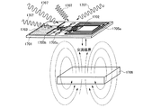
なお、内部アンテナ回路411は複数の周波数帯の電磁波を受信可能なマルチバンドアンテナ構造であってもよい。例えば、図30に示すように内部アンテナ回路が複数のアンテナ回路によって形成されていてもよい。図30に示す構造において、基板1701上に、第1のアンテナ回路1705a、第2のアンテナ回路1705b、第3のアンテナ回路1705cと、制御回路を有する回路素子1702と、バッテリ1703とを有している。なお、第1のアンテナ回路1705a、第2のアンテナ回路1705b、第3のアンテナ回路1705cと回路素子1702に設けられた制御回路とは電気的に接続されている。なお、1706はバッテリを充電するための電磁波を送信するための送信機であり、表示部等に設けられている。
Note that the
第1のアンテナ回路1705a、第2のアンテナ回路1705b、第3のアンテナ回路1705cにより受信された電磁波は、回路素子1702に形成された制御回路における整流回路を介してバッテリ1703に入力され、バッテリ1703が充電される。
The electromagnetic waves received by the
ここでは、送信機1706から送信された電磁波を第1のアンテナ回路1705aで受信し、外部の無線信号1707を第2のアンテナ回路1705b、第3のアンテナ回路1705cで受信している例を示している。また、第1のアンテナ回路1705a、第2のアンテナ回路1705b、第3のアンテナ回路1705cの接続関係については特に限定されず、例えば、全てのアンテナが電気的に接続されていてもよいし、それぞれが電気的に接続せず独立に設けられていてもよい。
Here, an example is shown in which an electromagnetic wave transmitted from the
なお、バッテリ1703の充電に用いられる第1のアンテナ回路1705a、第2のアンテナ回路1705b、第3のアンテナ回路1705cのアンテナの長さや形状は図30に示した構造に限られない。ここでは、第2のアンテナ回路1705b、第3のアンテナ回路1705cのアンテナとして、長さの異なる線状のアンテナ(ダイポールアンテナ)を設けた例を示したが、例えば、ダイポールアンテナとコイル状のアンテナを組み合わせて用いてもよいし、ダイポールアンテナとパッチアンテナを組み合わせて用いてもよい。このように、バッテリ1703の充電に用いられるアンテナとして、長さや形状の異なるものを複数設けることによって、様々な無線信号を受信することができるため、充電効率を向上させることができる。特に、パッチアンテナとダイポールアンテナ等の形状の異なるアンテナを組み合わせて設けることによって(例えば、パッチアンテナの周囲に折り返しダイポールアンテナを設ける)、限られたスペースを有効に活用することが可能となる。本実施の形態では、3つのアンテナ回路1705a、1705b、1705cを設けた例を示したが、これに限られず、1つのアンテナ回路又は3つ以上のアンテナ回路を設けた構成としてもよい。
Note that the lengths and shapes of the antennas of the
また、例えば、第1のアンテナ回路1705aと送信機1706間で送受信される信号として、125kHz、13.56MHz、915MHz、2.45GHzなどの周波数帯の信号を用いることができ、それぞれISO規格などが設定される。勿論、第1のアンテナ回路1705aと送信機1706間で送受信される信号の周波数はこれに限定されず、例えば、サブミリ波である300GHz〜3THz、ミリ波である30GHz〜300GHz、マイクロ波である3GHz〜30GHz、極超短波である300MHz〜3GHz、超短波である30MHz〜300MHz、短波である3MHz〜30MHz、中波である300kHz〜3MHz、長波である30kHz〜300kHz、及び超長波である3kHz〜30kHzのいずれの周波数も用いることができる。また、第1のアンテナ回路1705aと送信機1706間で送受信される信号は、搬送波を変調した信号である。搬送波の変調方式は、アナログ変調であってもデジタル変調であってよく、振幅変調、位相変調、周波数変調、及びスペクトラム拡散のいずれであってもよい。望ましくは、振幅変調、または、周波数変調にするとよい。
For example, as a signal transmitted and received between the
また、第2のアンテナ回路1705b、第3のアンテナ回路1705cのアンテナで受信する外部の無線信号1707として、例えば、携帯電話の中継局の電波帯(800〜900MHz帯、1.5GHz、1.9〜2.1GHz帯等)、携帯電話から発振される電波、電波時計の電波(40kHz等)、家庭用の交流電源のノイズ(60Hz等)、他のリーダ/ライタ等から無作為に生じている電波等を利用することができる。外部の無線信号を受信してバッテリの充電を無線で行うことによって、バッテリを充電するための充電器等を別途必要としないため、より低コストでバッテリを作製することができる。また、図30に示すように、それぞれ長さや形状の異なるアンテナを用いた複数のアンテナ回路を設けることによって、バッテリ1703の充電用として様々な無線信号を利用することができる。また、第2のアンテナ回路1705b、第3のアンテナ回路1705cに設けられるアンテナの形状は、これらの無線信号を受信しやすい長さや形状で設けるとよい。また、図30では、第1のアンテナ回路1705aは送信機1706からの電磁波を受信する形態としたが、これに限定されず全てのアンテナ回路で外部の無線信号を受信してバッテリを充電する形態としてもよい。
In addition, as an
なお、図30では、同一の基板1701上に複数のアンテナ回路1705a、1705b、1705c、回路素子1702及びバッテリ1703を設けた例を示したが、図30に示す構造に限られることはなく、それぞれを別々の基板上に設けてもよい。
FIG. 30 shows an example in which a plurality of
次いで、図27に示すバッテリ407として薄膜状のバッテリの構成例について説明する。本実施の形態では、リチウムイオン電池を用いた場合のバッテリの構成例を図31に示す。
Next, a configuration example of a thin film battery as the
図31は薄膜状のバッテリの断面模式図である。まず、基板7101上に電極となる集電体薄膜7102を成膜する。集電体薄膜7102は負極活物質層7103と密着性がよく、抵抗が小さいことが求められ、アルミニウム、銅、ニッケル、バナジウムなどを用いることができる。次に集電体薄膜7102上に負極活物質層7103を成膜する。一般には酸化バナジウム(V2O5)などが用いられる。次に負極活物質層7103上に固体電解質層7104を成膜する。一般にはリン酸リチウム(Li3PO4)などが用いられる。次に固体電解質層7104上に正極活物質層7105を成膜する。一般にはマンガン酸リチウム(LiMn2O4)などが用いられる。コバルト酸リチウム(LiCoO2)やニッケル酸リチウム(LiNiO2)を用いても良い。次に正極活物質層7105上に電極となる集電体薄膜7106を成膜する。集電体薄膜7106は正極活物質層7105と密着性がよく、抵抗が小さいことが求められ、アルミニウム、銅、ニッケル、バナジウムなどを用いることができる。なお、リチウムイオン電池は、ニッカド電池、鉛電池などと比べて、メモリ効果がなく、電流量を大きく取ることができる。 FIG. 31 is a schematic cross-sectional view of a thin film battery. First, a current collector thin film 7102 to be an electrode is formed over the substrate 7101. The current collector thin film 7102 is required to have good adhesion to the negative electrode active material layer 7103 and low resistance, and aluminum, copper, nickel, vanadium, or the like can be used. Next, a negative electrode active material layer 7103 is formed over the current collector thin film 7102. In general, vanadium oxide (V 2 O 5 ) or the like is used. Next, a solid electrolyte layer 7104 is formed over the negative electrode active material layer 7103. In general, lithium phosphate (Li 3 PO 4 ) or the like is used. Next, a positive electrode active material layer 7105 is formed over the solid electrolyte layer 7104. Generally, lithium manganate (LiMn 2 O 4 ) or the like is used. Lithium cobaltate (LiCoO2) or lithium nickel oxide (LiNiO 2) may be used. Next, a current collector thin film 7106 to be an electrode is formed over the positive electrode active material layer 7105. The current collector thin film 7106 is required to have good adhesion to the positive electrode active material layer 7105 and low resistance, and aluminum, copper, nickel, vanadium, or the like can be used. Note that a lithium ion battery has no memory effect and can take a larger amount of current than a nickel cadmium battery or a lead battery.
また、上記集電体薄膜7102、負極活物質層7103、固体電解質層7104、正極活物質層7105、集電体薄膜7106の薄膜層は、スパッタ技術を用いて形成しても良いし、蒸着技術を用いても良い。また集電体薄膜7102、負極活物質層7103、固体電解質層7104、正極活物質層7105、集電体薄膜7106のそれぞれの厚さは0.1μm〜3μmが望ましい。 The thin film layers of the current collector thin film 7102, the negative electrode active material layer 7103, the solid electrolyte layer 7104, the positive electrode active material layer 7105, and the current collector thin film 7106 may be formed using a sputtering technique or a vapor deposition technique. May be used. The thickness of each of the current collector thin film 7102, the negative electrode active material layer 7103, the solid electrolyte layer 7104, the positive electrode active material layer 7105, and the current collector thin film 7106 is preferably 0.1 μm to 3 μm.
次に以下に充電時、放電時の動作を説明する。充電時には、正極活物質層7105からリチウムがイオンとなって離脱する。そのリチウムイオンは固体電解質層7104を介して負極活物質層7103に吸収される。このときに、正極活物質層7105から外部へ電子が放出される。 Next, the operation during charging and discharging will be described below. At the time of charging, lithium is released from the positive electrode active material layer 7105 as ions. The lithium ions are absorbed by the negative electrode active material layer 7103 through the solid electrolyte layer 7104. At this time, electrons are emitted from the positive electrode active material layer 7105 to the outside.
また放電時には、負極活物質層7103からリチウムがイオンとなって離脱する。そのリチウムイオンは固体電解質層7104を介して、正極活物質層7105に吸収される。このとき負極活物質層7103から外部に電子が放出される。この様にして薄膜二次電池は動作する。 Further, during discharge, lithium is released from the negative electrode active material layer 7103 as ions. The lithium ions are absorbed by the positive electrode active material layer 7105 through the solid electrolyte layer 7104. At this time, electrons are emitted from the negative electrode active material layer 7103 to the outside. In this way, the thin film secondary battery operates.
なお、再度集電体薄膜7102、負極活物質層7103、固体電解質層7104、正極活物質層7105、集電体薄膜7106の薄膜層を重ねて形成することで、より大きい電力の充放電が可能になるため好適である。 Note that by forming the current collector thin film 7102, the negative electrode active material layer 7103, the solid electrolyte layer 7104, the positive electrode active material layer 7105, and the current collector thin film 7106 again, charging and discharging with higher power is possible. This is preferable.
本実施の形態のバッテリは厚さ10μm以下程度の薄膜状であり、且つ充放電可能なバッテリであるため、本実施の形態のバッテリを用いることにより小型で軽量な半導体装置を作製することができる。 Since the battery of this embodiment is a thin film with a thickness of about 10 μm or less and is a chargeable / dischargeable battery, a small and lightweight semiconductor device can be manufactured by using the battery of this embodiment. .
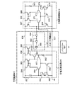
バッテリとして充電可能な電池を使用する場合、一般に、充放電の制御が必要である。つまり、充電をおこなう際に過充電にならないように、充電状況をモニターしながら充電を行う必要がある。本実施の形態において、充電制御をおこなうための回路について説明する。図32に、図27に示した充電回路413、充電制御回路414、バッテリ407のブロック図を示す。
When a rechargeable battery is used as a battery, it is generally necessary to control charging and discharging. In other words, it is necessary to perform charging while monitoring the charging status so as not to overcharge when charging. In this embodiment, a circuit for performing charge control will be described. FIG. 32 is a block diagram of the charging circuit 413, the charging control circuit 414, and the
図32に示す例では充電回路413は定電流源回路425、スイッチ回路426から構成され、充電制御回路414、バッテリ407と電気的に接続されている。なお、図32に示す充電回路は一例であり、この様な構成に限定されるものではなく、他の構成であっても良い。本実施の形態は定電流によって、バッテリ407に充電をおこなっているが、定電流だけの充電ではなく、途中で定電圧充電に切り替えても良い。定電流を用いない別の方式であっても良い。また、以下の回路を構成するトランジスタは薄膜トランジスタであっても良いし、単結晶基板上のトランジスタや有機トランジスタであっても良い。
In the example shown in FIG. 32, the charging circuit 413 includes a constant
図33は図32の回路をさらに詳細にしたものである。以下に動作を説明する。定電流源回路425、スイッチ回路426、充電制御回路414は高電位電源線976、低電位電源線977を電源線として用いている。図33では低電位電源線977をGND線として用いているが、GND線には限定されず他の電位であっても良い。
FIG. 33 shows the circuit of FIG. 32 in more detail. The operation will be described below. The constant
定電流源回路425はトランジスタ952〜961、抵抗951、962によって構成されている。高電位電源線976より抵抗951を介してトランジスタ952、953に電流が流れ、トランジスタ952、953がオン(ON)する。
The constant
トランジスタ954、955、956、957、958は帰還型の差動アンプを構成し、トランジスタ952のゲート電位はトランジスタ956のゲート電位とほぼ同じとなる。トランジスタ961のドレイン電流はトランジスタ957のゲート電位と低電位電源線977の差電位を抵抗962の抵抗値で割った値となる。その電流をトランジスタ959、960によって構成されるカレントミラー回路に入力し、カレントミラー回路の出力電流をスイッチ回路426に供給する。定電流源回路425は本構成に限定されず他の構成を用いても良い。
The
スイッチ回路426はトランスミッションゲート965、インバータ963,964から構成され、インバータ964の入力信号によって定電流源回路425の電流をバッテリ407に供給するか、否かを制御する。スイッチ回路はこの構成に限定されず他の構成を用いても良い。
The switch circuit 426 includes a
充電制御回路414はトランジスタ966〜974、抵抗975によって構成される。高電位電源線976より抵抗975を介してトランジスタ973、974に電流が流れ、トランジスタ973、974がオン(ON)する。トランジスタ968、969、970、971、972は差動型のコンパレーターを構成している。トランジスタ970のゲート電位がトランジスタ971のゲート電位より低い場合、トランジスタ968のドレイン電位はほぼ高電位電源線976の電位とほぼ等しくなり、トランジスタ970のゲート電位がトランジスタ971のゲート電位より高い場合、トランジスタ968のドレイン電位はトランジスタ970のソース電位とほぼ等しくなる。
The charge control circuit 414 includes
トランジスタ968のドレイン電位が高電位電源線976とほぼ等しい場合、トランジスタ967、966で構成されるバッファを介して、充電制御回路414はロウを出力する。トランジスタ968のドレイン電位がトランジスタ970のソース電位とほぼ等しい場合、トランジスタ967、966で構成されるバッファを介して、充電制御回路414はハイを出力する。
When the drain potential of the
充電制御回路414の出力がロウの場合、バッテリ407にはスイッチ回路426を介して電流が供給される。また、充電制御回路414の出力がハイの場合は、スイッチ回路426はオフ(OFF)して、バッテリ407に電流は供給されない。トランジスタ970のゲートはバッテリ407に電気的に接続されているため、バッテリ407が充電され、その電位が充電制御回路414のコンパレータのしきい値を超えると、充電が停止する。本実施の形態ではコンパレータのしきい値をトランジスタ973のゲート電位で設定しているが、この値に限定するものではなく、他の電位であっても良い。一般に設定電位は用途とバッテリの性能によって適宜決められるものである。なお、バッテリへの充電回路の構成は、この構成に限定されるものではない。
When the output of the charge control circuit 414 is low, current is supplied to the
[実施の形態5]
本実施の形態では、本発明により得られた光電変換装置を様々な電子機器に組み込んだ例について説明する。本発明が適用される電子機器として、コンピュータ、ディスプレイ、携帯電話、テレビなどが挙げられる。それらの電子機器の具体例を、図19、図20(A)〜図20(B)、図21(A)〜図21(B)、図22及び図23に示す。
[Embodiment 5]
In this embodiment, examples in which the photoelectric conversion device obtained according to the present invention is incorporated into various electronic devices will be described. Examples of electronic devices to which the present invention is applied include computers, displays, mobile phones, and televisions. Specific examples of these electronic devices are shown in FIGS. 19, 20A to 20B, 21A to 21B, 22 and 23. FIG.
図19は携帯電話であり、本体(A)701、本体(B)702、筐体703、操作キー704、音声入力部705、音声出力部706、回路基板707、表示パネル(A)708、表示パネル(B)709、蝶番710、透光性材料部711、光電変換素子712を有している。本発明は光電変換素子712に適用することができる。
FIG. 19 shows a cellular phone, which includes a main body (A) 701, a main body (B) 702, a
光電変換素子712は透光性材料部711を透過した光を検知し、検知した外部光の照度に合わせて表示パネル(A)708及び表示パネル(B)709の輝度コントロールを行ったり、光電変換素子712で得られる照度に合わせて操作キー704の照明制御を行う。これにより携帯電話の消費電流を抑えることができる。
The
図20(A)及び図20(B)に携帯電話の別の例を示す。図20(A)及び図20(B)において、721は本体、722は筐体、723は表示パネル、724は操作キー、725は音声出力部、726は音声入力部、727及び728は光電変換素子である。 20A and 20B illustrate another example of a mobile phone. 20A and 20B, 721 is a main body, 722 is a housing, 723 is a display panel, 724 is an operation key, 725 is an audio output unit, 726 is an audio input unit, and 727 and 728 are photoelectric conversions. It is an element.
図20(A)に示す携帯電話では、本体721に設けられた光電変換素子727により外部の光を検知することにより表示パネル723及び操作キー724の輝度を制御することが可能である。
In the cellular phone illustrated in FIG. 20A, the luminance of the
また図20(B)に示す携帯電話では、図20(A)の構成に加えて、本体721の内部に光電変換素子728を設けている。光電変換素子728により、表示パネル723に設けられているバックライトの輝度を検出することも可能となる。
In addition, in the cellular phone illustrated in FIG. 20B, a
図21(A)はコンピュータであり、本体731、筐体732、表示部733、キーボード734、外部接続ポート735、ポインティングデバイス736等を含む。
FIG. 21A illustrates a computer, which includes a
また図21(B)は表示装置でありテレビ受像器などがこれに当たる。本表示装置は、筐体741、支持台742、表示部743などによって構成されている。
FIG. 21B shows a display device such as a television receiver. This display device includes a
図21(A)のコンピュータに設けられる表示部733、及び図21(B)に示す表示装置の表示部743として、液晶パネルを用いた場合の詳しい構成を図22に示す。
FIG. 22 shows a detailed structure in the case where a liquid crystal panel is used as the
図22に示す液晶パネル762は、筐体761に内蔵されており、基板751a及び751b、基板751a及び751bに挟まれた液晶層752、偏光フィルタ755a及び755b、及びバックライト753等を有している。また筐体761には光電変換素子を有する光電変換素子形成領域754が形成されている。
A
本発明を用いて作製された光電変換素子形成領域754はバックライト753からの光量を感知し、その情報がフィードバックされて液晶パネル762の輝度が調節される。
The photoelectric conversion
図23(A)及び図23(B)は、本発明の光センサをカメラ、例えばデジタルカメラに組み込んだ例を示す図である。図23(A)は、デジタルカメラの前面方向から見た斜視図、図23(B)は、後面方向から見た斜視図である。図23(A)において、デジタルカメラには、リリースボタン801、メインスイッチ802、ファインダ窓803、フラッシュ804、レンズ805、鏡胴806、筺体807が備えられている。
FIG. 23A and FIG. 23B are diagrams showing an example in which the optical sensor of the present invention is incorporated in a camera, for example, a digital camera. FIG. 23A is a perspective view seen from the front side of the digital camera, and FIG. 23B is a perspective view seen from the rear side. In FIG. 23A, the digital camera includes a
また、図23(B)において、ファインダ接眼窓811、モニタ812、操作ボタン813が備えられている。
In FIG. 23B, a
リリースボタン801は、半分の位置まで押下されると、焦点調整機構および露出調整機構が作動し、最下部まで押下されるとシャッターボタンが開く。
When the
メインスイッチ802は、押下又は回転によりデジタルカメラの電源のON/OFFを切り替える。
A
ファインダ窓803は、デジタルカメラの前面のレンズ805の上部に配置されており、図23(B)に示すファインダ接眼窓811から撮影する範囲やピントの位置を確認するための装置である。
The
フラッシュ804は、デジタルカメラの前面上部に配置され、被写体輝度が低いときに、リリースボタンが押下されてシャッターボタンが開くと同時に補助光を照射する。
The
レンズ805は、デジタルカメラの正面に配置されている。レンズは、フォーカシングレンズ、ズームレンズ等により構成され、図示しないシャッターボタン及び絞りと共に撮影光学系を構成する。また、レンズの後方には、CCD(Charge Coupled Device)等の撮像素子が設けられている。
The
鏡胴806は、フォーカシングレンズ、ズームレンズ等のピントを合わせるためにレンズの位置を移動するものであり、撮影時には、鏡胴を繰り出すことにより、レンズ805を手前に移動させる。また、携帯時は、レンズ805を沈銅させてコンパクトにする。なお、本実施の形態においては、鏡胴を繰り出すことにより被写体をズーム撮影することができる構造としているが、この構造に限定されるものではなく、筺体807内での撮影光学系の構成により鏡胴を繰り出さずともズーム撮影が可能なデジタルカメラでもよい。
The
ファインダ接眼窓811は、デジタルカメラの後面上部に設けられており、撮影する範囲やピントの位置を確認する際に接眼するために設けられた窓である。
The
操作ボタン813は、デジタルカメラの後面に設けられた各種機能ボタンであり、セットアップボタン、メニューボタン、ディスプレイボタン、機能ボタン、選択ボタン等により構成されている。
The
本発明の光センサを図23(A)及び図23(B)に示すカメラに組み込むと、光センサが光の有無及び強さを感知することができ、これによりカメラの露出調整等を行うことができる。 When the optical sensor of the present invention is incorporated in the camera shown in FIGS. 23A and 23B, the optical sensor can detect the presence and intensity of light, thereby adjusting the exposure of the camera. Can do.
また本発明の光センサはその他の電子機器、例えばプロジェクションテレビ、ナビゲーションシステム等に応用することが可能である。すなわち光を検出する必要のあるものであればいかなるものにも用いることが可能である。 The optical sensor of the present invention can be applied to other electronic devices such as a projection television and a navigation system. In other words, it can be used for any object that needs to detect light.
なお本実施の形態は、必要であれば他の実施の形態と組み合わせてもよい。 Note that this embodiment may be combined with other embodiments if necessary.
本実施例では、図1のTFT104のソース電極またはドレイン電極を形成する導電膜の膜厚を変えたときの、照度Eと光電流Iとの関係を、図24及び図25に示す。
In this example, FIGS. 24 and 25 show the relationship between the illuminance E and the photocurrent I when the film thickness of the conductive film forming the source electrode or the drain electrode of the
図24は、照度E(横軸)とゲート電極にかかる電圧Vgate(縦軸)の関係を示すグラフであり、ソース電極またはドレイン電極の膜厚を、シート抵抗が0.052Ω/□、0.52Ω/□、5.2Ω/□、52Ω/□、520Ω/□(抵抗比:0.01、0.1、1、10、100)となるように形成したものの比較を示す。 FIG. 24 is a graph showing the relationship between the illuminance E (horizontal axis) and the voltage V gate (vertical axis) applied to the gate electrode. The film thickness of the source electrode or drain electrode is 0.052Ω / □, 0 A comparison is made between those formed to have a resistance ratio of .52Ω / □, 5.2Ω / □, 52Ω / □, and 520Ω / □ (resistance ratio: 0.01, 0.1, 1, 10, 100).
図25は、照度E(横軸)と倍率(縦軸)の関係を示すグラフであり、倍率とは図24の光電流Iの微分値である。 FIG. 25 is a graph showing the relationship between the illuminance E (horizontal axis) and the magnification (vertical axis), and the magnification is a differential value of the photocurrent I in FIG.
なお図24及び図25において、白抜き菱形は抵抗比0.01(シート抵抗:0.052Ω/□)、白抜き四角形は抵抗比0.1(シート抵抗:0.52Ω/□)、白抜き三角形は抵抗比1(シート抵抗:5.2Ω/□)、白抜き丸形は抵抗比10(シート抵抗:52Ω/□)、黒塗り四角形は抵抗比100(シート抵抗:520Ω/□)を表している。 24 and 25, the white diamonds have a resistance ratio of 0.01 (sheet resistance: 0.052 Ω / □), and the white squares have a resistance ratio of 0.1 (sheet resistance: 0.52 Ω / □) and white. The triangle represents the resistance ratio 1 (sheet resistance: 5.2 Ω / □), the white circle represents the resistance ratio 10 (sheet resistance: 52 Ω / □), and the black square represents the resistance ratio 100 (sheet resistance: 520 Ω / □). ing.
図24及び図25に示されるように、ソース電極またはドレイン電極の抵抗値が低い、0.052Ω/□、0.52Ω/□、5.2Ω/□(抵抗比:0.01、0.1、1)では、光電流Iは照度Eが高くなっても低減する割合が小さい。しかしながら、一方、ソース電極またはドレイン電極の抵抗値が高い、52Ω/□、520Ω/□(抵抗比:10、100)では、照度Eが大きくなると、大きく低減することが分かる。 As shown in FIGS. 24 and 25, the resistance value of the source electrode or the drain electrode is low, 0.052Ω / □, 0.52Ω / □, 5.2Ω / □ (resistance ratio: 0.01, 0.1 In 1), the rate of reduction of the photocurrent I is small even when the illuminance E increases. However, it can be seen that, at 52Ω / □, 520Ω / □ (resistance ratio: 10, 100) where the resistance value of the source electrode or the drain electrode is high, the illuminance E increases greatly.
以上から、カレントミラー回路の参照側のTFT104に寄生抵抗が発生してしまうと、出力される光電流が減少してしまうことが分かる。これにより感知する光強度の範囲が減少してしまうので、本発明の構成は寄生抵抗の発生を抑制し、光感度の減少を防ぐことができるので有用である。
From the above, it can be seen that if a parasitic resistance occurs in the
本発明により、光感度の低下を抑制することが可能な、半導体装置や光電変換装置を作製することができる。また本発明の半導体装置や光電変換装置を組み込むことにより、回路動作の安定性や信頼性の高い電気機器を得ることが可能である。 According to the present invention, a semiconductor device or a photoelectric conversion device that can suppress a decrease in photosensitivity can be manufactured. Further, by incorporating the semiconductor device or the photoelectric conversion device of the present invention, it is possible to obtain an electric device with high stability and reliability of circuit operation.
100 光電変換層
100i i型半導体層
100n n型半導体層
100p p型半導体層
101 電源
103 光電変換層
103i i型半導体層
103n n型半導体層
103p p型半導体層
104 TFT
105 TFT
105a TFT
105i TFT
111 カレントミラー回路
118a 回路
118b 回路
118i 回路
119a 端子
119b 端子
119i 端子
120a 端子
120b 端子
120i 端子
121a 端子
121b 端子
121i 端子
122 カレントミラー回路
123 回路
124 端子
141 電極
142 電極
144 配線
145 配線
146 配線
146a 配線
146b 配線
146c 配線
146d 配線
147 配線
201 TFT
202 TFT
203 カレントミラー回路
204 回路
210 基板
212 下地絶縁膜
213 ゲート絶縁膜
214 配線
215 配線
216 絶縁膜
217 絶縁膜
218 保護電極
219 配線
220 接続電極
221 端子電極
222 端子電極
224 封止層
231 島状半導体領域
232 島状半導体領域
234 ゲート電極
235 ゲート電極
237 ソース領域またはドレイン領域
238 ソース領域またはドレイン領域
241 ソース電極またはドレイン電極
242 ソース電極またはドレイン電極
245 保護電極
246 保護電極
247 保護電極
248 保護電極
250 端子電極
251 端子電極
260 基板
261 電極
262 電極
263 半田
264 半田
271 ソース領域またはドレイン領域
272 ソース領域またはドレイン領域
281 端子電極
282 ソース電極またはドレイン電極
283 ソース電極またはドレイン電極
284 配線
285 接続電極
291 素子形成領域
292 受光部
293 増幅回路部
301 TFT
302 TFT
303 カレントミラー回路
311 金属膜
312 ゲート電極
313 ゲート電極
314 ゲート絶縁膜
315 島状半導体領域
316 島状半導体領域
318 マスク
321 ソース領域またはドレイン領域
322 ソース領域またはドレイン領域
331 ソース電極またはドレイン電極
332 ソース電極またはドレイン電極
336 保護電極
337 保護電極
341 ソース電極またはドレイン電極
342 ソース電極またはドレイン電極
401 RFバッテリ
407 バッテリ
411 内部アンテナ回路
412 整流回路
413 充電回路
414 充電制御回路
415 外部アンテナ回路
425 定電流源回路
426 スイッチ回路
501 アンテナ
502 共振容量
503 アンテナ回路
504 ダイオード
505 ダイオード
506 平滑容量
522 回路素子
523 アンテナ
701 本体(A)
702 本体(B)
703 筐体
704 操作キー
705 音声入力部
706 音声出力部
707 回路基板
708 表示パネル(A)
709 表示パネル(B)
710 蝶番
711 透光性材料部
712 光電変換素子
712 光電変換素子
721 本体
722 筐体
723 表示パネル
724 操作キー
725 音声出力部
726 音声入力部
727 光電変換素子
728 光電変換素子
731 本体
732 筐体
733 表示部
734 キーボード
735 外部接続ポート
736 ポインティングデバイス
741 筐体
742 支持台
743 表示部
751a 基板
751b 基板
752 液晶層
753 バックライト
754 光電変換素子形成領域
755a 偏光フィルタ
755b 偏光フィルタ
761 筐体
762 液晶パネル
801 リリースボタン
802 メインスイッチ
803 ファインダ窓
804 フラッシュ
805 レンズ
806 鏡胴
807 筺体
811 ファインダ接眼窓
812 モニタ
813 操作ボタン
951 抵抗
952 トランジスタ
953 トランジスタ
954 トランジスタ
955 トランジスタ
956 トランジスタ
957 トランジスタ
958 トランジスタ
959 トランジスタ
960 トランジスタ
961 トランジスタ
962 抵抗
963 インバータ
964 インバータ
965 トランスミッションゲート
966 トランジスタ
967 トランジスタ
968 トランジスタ
969 トランジスタ
970 トランジスタ
971 トランジスタ
972 トランジスタ
973 トランジスタ
974 トランジスタ
975 抵抗
976 高電位電源線
977 低電位電源線
1001 電源
1003 フォトダイオード
1004 TFT
1005 TFT
1006 寄生抵抗
1011 カレントミラー回路
1701 基板
1702 回路素子
1703 バッテリ
1705a アンテナ回路
1705b アンテナ回路
1705c アンテナ回路
1706 送信機
1707 無線信号
7101 基板
7102 集電体薄膜
7103 負極活物質層
7104 固体電解質層
7105 正極活物質層
7106 集電体薄膜
RL 負荷抵抗
100 photoelectric conversion layer 100i i-type semiconductor layer 100n n-type semiconductor layer 100p p-
105 TFT
105a TFT
105i TFT
111
202 TFT
203
302 TFT
303
702 Body (B)
703
709 Display panel (B)
710
1005 TFT
1006
Claims (19)
参照用の薄膜トランジスタと出力側の薄膜トランジスタとを有し、前記光電変換素子の出力を増幅するカレントミラー回路と、
高電位電極と低電位電極とを有する電源と、
を有し、
前記参照用の薄膜トランジスタ及び前記出力側の薄膜トランジスタはn型の薄膜トランジスタであり、
前記参照用の薄膜トランジスタのソース電極及びドレイン電極の一方は前記光電変換素子を介して前記高電位電極と電気的に接続され、
前記出力側の薄膜トランジスタのソース電極及びドレイン電極の一方は前記高電位電極と電気的に接続され、
前記参照用の薄膜トランジスタのソース電極及びドレイン電極の他方は前記低電位電極と電気的に接続され、
前記出力側の薄膜トランジスタのソース電極及びドレイン電極の他方は前記低電位電極と電気的に接続され、
前記参照側の薄膜トランジスタは、前記出力側の薄膜トランジスタよりも前記低電位電極と近いところに配置されることを特徴とする半導体装置。 A photoelectric conversion element;
A current mirror circuit that has a thin film transistor for reference and a thin film transistor on the output side, and amplifies the output of the photoelectric conversion element;
A power source having a high potential electrode and a low potential electrode;
Have
The reference thin film transistor and the output side thin film transistor are n-type thin film transistors,
One of a source electrode and a drain electrode of the reference thin film transistor is electrically connected to the high potential electrode through the photoelectric conversion element,
One of a source electrode and a drain electrode of the thin film transistor on the output side is electrically connected to the high potential electrode,
The other of the source electrode and the drain electrode of the reference thin film transistor is electrically connected to the low potential electrode,
The other of the source electrode and the drain electrode of the output side thin film transistor is electrically connected to the low potential electrode,
The semiconductor device according to claim 1, wherein the thin film transistor on the reference side is disposed closer to the low potential electrode than the thin film transistor on the output side.
前記参照側の薄膜トランジスタのソース電極及びドレイン電極の一方は、前記出力側の薄膜トランジスタのソース電極及びドレイン電極の一方に前記光電変換素子を介して電気的に接続され、
前記参照側の薄膜トランジスタのソース電極及びドレイン電極の他方は、前記出力側の薄膜トランジスタのソース電極及びドレイン電極の他方に電気的に接続されていることを特徴とする半導体装置。 In Claim 1, the gate electrode of the thin film transistor on the output side is electrically connected to one of the gate electrode of the thin film transistor on the reference side and the source electrode and drain electrode of the thin film transistor on the reference side,
One of the source electrode and the drain electrode of the thin film transistor on the reference side is electrically connected to one of the source electrode and the drain electrode of the thin film transistor on the output side via the photoelectric conversion element,
The other of the source electrode and the drain electrode of the thin film transistor on the reference side is electrically connected to the other of the source electrode and the drain electrode of the thin film transistor on the output side.
参照用の薄膜トランジスタと出力側の薄膜トランジスタとを有し、前記光電変換素子の出力を増幅するカレントミラー回路と、
高電位電極と低電位電極とを有する電源と、
を有し、
前記参照用の薄膜トランジスタ及び前記出力側の薄膜トランジスタはn型の薄膜トランジスタであり、
前記参照用の薄膜トランジスタのソース電極及びドレイン電極の一方は前記光電変換素子を介して前記高電位電極と電気的に接続され、
前記出力側の薄膜トランジスタのソース電極及びドレイン電極の一方は前記高電位電極と電気的に接続され、
前記参照用の薄膜トランジスタのソース電極及びドレイン電極の他方は前記低電位電極と電気的に接続され、
前記出力側の薄膜トランジスタのソース電極及びドレイン電極の他方は前記低電位電極と電気的に接続され、
前記参照側の薄膜トランジスタと前記低電位電極との間の電流経路は、前記出力側の薄膜トランジスタと前記低電位電極との間の電流経路よりも短いことを特徴とする半導体装置。 A photoelectric conversion element;
A current mirror circuit that has a thin film transistor for reference and a thin film transistor on the output side, and amplifies the output of the photoelectric conversion element;
A power source having a high potential electrode and a low potential electrode;
Have
The reference thin film transistor and the output side thin film transistor are n-type thin film transistors,
One of a source electrode and a drain electrode of the reference thin film transistor is electrically connected to the high potential electrode through the photoelectric conversion element,
One of a source electrode and a drain electrode of the thin film transistor on the output side is electrically connected to the high potential electrode,
The other of the source electrode and the drain electrode of the reference thin film transistor is electrically connected to the low potential electrode,
The other of the source electrode and the drain electrode of the output side thin film transistor is electrically connected to the low potential electrode,
A semiconductor device, wherein a current path between the reference-side thin film transistor and the low-potential electrode is shorter than a current path between the output-side thin film transistor and the low-potential electrode.
前記参照側の薄膜トランジスタのソース電極及びドレイン電極の一方は、前記出力側の薄膜トランジスタのソース電極及びドレイン電極の一方に前記光電変換素子を介して電気的に接続され、
前記参照側の薄膜トランジスタのソース電極及びドレイン電極の他方は、前記出力側の薄膜トランジスタのソース電極及びドレイン電極の他方に電気的に接続されていることを特徴とする半導体装置。 The gate electrode of the output side thin film transistor is electrically connected to one of the gate electrode of the reference side thin film transistor and the source electrode and the drain electrode of the reference side thin film transistor according to claim 3,
One of the source electrode and the drain electrode of the thin film transistor on the reference side is electrically connected to one of the source electrode and the drain electrode of the thin film transistor on the output side via the photoelectric conversion element,
The other of the source electrode and the drain electrode of the thin film transistor on the reference side is electrically connected to the other of the source electrode and the drain electrode of the thin film transistor on the output side.
参照用の薄膜トランジスタと複数の出力側の薄膜トランジスタとを有し、前記光電変換素子の出力を増幅するカレントミラー回路と、
高電位電極と低電位電極とを有する電源と、
を有し、
前記参照用の薄膜トランジスタ及び前記複数の出力側の薄膜トランジスタはn型の薄膜トランジスタであり、
前記参照用の薄膜トランジスタのソース電極及びドレイン電極の一方は前記光電変換素子を介して前記高電位電極と電気的に接続され、
前記複数の出力側の薄膜トランジスタのソース電極及びドレイン電極の一方は前記高電位電極と電気的に接続され、
前記参照用の薄膜トランジスタのソース電極及びドレイン電極の他方は前記低電位電極と電気的に接続され、
前記複数の出力側の薄膜トランジスタのソース電極及びドレイン電極の他方は前記低電位電極と電気的に接続され、
前記参照側の薄膜トランジスタは、前記複数の出力側の薄膜トランジスタのそれぞれよりも前記低電位電極と近いところに配置されることを特徴とする半導体装置。 A photoelectric conversion element;
A current mirror circuit that has a thin film transistor for reference and a plurality of thin film transistors on the output side, and amplifies the output of the photoelectric conversion element;
A power source having a high potential electrode and a low potential electrode;
Have
The reference thin film transistor and the plurality of output-side thin film transistors are n-type thin film transistors,
One of a source electrode and a drain electrode of the reference thin film transistor is electrically connected to the high potential electrode through the photoelectric conversion element,
One of the source electrode and the drain electrode of the plurality of output side thin film transistors is electrically connected to the high potential electrode,
The other of the source electrode and the drain electrode of the reference thin film transistor is electrically connected to the low potential electrode,
The other of the source electrode and the drain electrode of the plurality of output side thin film transistors is electrically connected to the low potential electrode,
The reference side thin film transistor is disposed closer to the low potential electrode than each of the plurality of output side thin film transistors.
前記参照側の薄膜トランジスタのソース電極及びドレイン電極の一方は、前記複数の出力側の薄膜トランジスタのソース電極及びドレイン電極の一方に前記光電変換素子を介して電気的に接続され、
前記参照側の薄膜トランジスタのソース電極及びドレイン電極の他方は、前記複数の出力側の薄膜トランジスタのソース電極及びドレイン電極の他方に電気的に接続されていることを特徴とする半導体装置。 The gate electrode of the plurality of output-side thin film transistors is electrically connected to one of the gate electrode of the reference-side thin film transistor and the source electrode and the drain electrode of the reference-side thin film transistor according to claim 5,
One of the source electrode and the drain electrode of the reference-side thin film transistor is electrically connected to one of the source electrode and the drain electrode of the plurality of output-side thin film transistors via the photoelectric conversion element,
The other of the source electrode and the drain electrode of the thin film transistor on the reference side is electrically connected to the other of the source electrode and the drain electrode of the plurality of thin film transistors on the output side.
参照用の薄膜トランジスタと複数の出力側の薄膜トランジスタとを有し、前記光電変換素子の出力を増幅するカレントミラー回路と、
高電位電極と低電位電極とを有する電源と、
を有し、
前記参照用の薄膜トランジスタ及び前記複数の出力側の薄膜トランジスタはn型の薄膜トランジスタであり、
前記参照用の薄膜トランジスタのソース電極及びドレイン電極の一方は前記光電変換素子を介して前記高電位電極と電気的に接続され、
前記複数の出力側の薄膜トランジスタのソース電極及びドレイン電極の一方は前記高電位電極と電気的に接続され、
前記参照用の薄膜トランジスタのソース電極及びドレイン電極の他方は前記低電位電極と電気的に接続され、
前記複数の出力側の薄膜トランジスタのソース電極及びドレイン電極の他方は前記低電位電極と電気的に接続され、
前記参照側の薄膜トランジスタと前記低電位電極との間の電流経路は、前記複数の出力側の薄膜トランジスタのそれぞれと前記低電位電極との間の電流経路よりも短いことを特徴とする半導体装置。 A photoelectric conversion element;
A current mirror circuit that has a thin film transistor for reference and a plurality of thin film transistors on the output side, and amplifies the output of the photoelectric conversion element;
A power source having a high potential electrode and a low potential electrode;
Have
The reference thin film transistor and the plurality of output-side thin film transistors are n-type thin film transistors,
One of a source electrode and a drain electrode of the reference thin film transistor is electrically connected to the high potential electrode through the photoelectric conversion element,
One of the source electrode and the drain electrode of the plurality of output side thin film transistors is electrically connected to the high potential electrode,
The other of the source electrode and the drain electrode of the reference thin film transistor is electrically connected to the low potential electrode,
The other of the source electrode and the drain electrode of the plurality of output side thin film transistors is electrically connected to the low potential electrode,
2. A semiconductor device according to claim 1, wherein a current path between the reference-side thin film transistor and the low-potential electrode is shorter than a current path between each of the plurality of output-side thin film transistors and the low-potential electrode.
前記参照側の薄膜トランジスタのソース電極及びドレイン電極の一方は、前記複数の出力側の薄膜トランジスタのソース電極及びドレイン電極の一方に前記光電変換素子を介して電気的に接続され、
前記参照側の薄膜トランジスタのソース電極及びドレイン電極の他方は、前記複数の出力側の薄膜トランジスタのソース電極及びドレイン電極の他方に電気的に接続されていることを特徴とする半導体装置。 The gate electrode of the plurality of output-side thin film transistors is electrically connected to one of the gate electrode of the reference-side thin film transistor and the source electrode and the drain electrode of the reference-side thin film transistor according to claim 7,
One of the source electrode and the drain electrode of the reference-side thin film transistor is electrically connected to one of the source electrode and the drain electrode of the plurality of output-side thin film transistors via the photoelectric conversion element,
The other of the source electrode and the drain electrode of the thin film transistor on the reference side is electrically connected to the other of the source electrode and the drain electrode of the plurality of thin film transistors on the output side.
参照用の薄膜トランジスタと出力側の薄膜トランジスタとを有し、前記光電変換素子の出力を増幅するカレントミラー回路と、
高電位電極と低電位電極とを有する電源と、
を有し、
前記参照用の薄膜トランジスタ及び前記出力側の薄膜トランジスタはp型の薄膜トランジスタであり、
前記参照用の薄膜トランジスタのソース電極及びドレイン電極の一方は前記高電位電極と電気的に接続され、
前記出力側の薄膜トランジスタのソース電極及びドレイン電極の一方は前記高電位電極と電気的に接続され、
前記参照用の薄膜トランジスタのソース電極及びドレイン電極の他方は前記光電変換素子を介して前記低電位電極と電気的に接続され、
前記出力側の薄膜トランジスタのソース電極及びドレイン電極の他方は前記低電位電極と電気的に接続され、
前記参照側の薄膜トランジスタは、前記出力側の薄膜トランジスタよりも前記高電位電極と近いところに配置されることを特徴とする半導体装置。 A photoelectric conversion element;
A current mirror circuit that has a thin film transistor for reference and a thin film transistor on the output side, and amplifies the output of the photoelectric conversion element;
A power source having a high potential electrode and a low potential electrode;
Have
The reference thin film transistor and the output thin film transistor are p-type thin film transistors,
One of a source electrode and a drain electrode of the reference thin film transistor is electrically connected to the high potential electrode,
One of a source electrode and a drain electrode of the thin film transistor on the output side is electrically connected to the high potential electrode,
The other of the source electrode and the drain electrode of the reference thin film transistor is electrically connected to the low potential electrode through the photoelectric conversion element,
The other of the source electrode and the drain electrode of the output side thin film transistor is electrically connected to the low potential electrode,
The semiconductor device according to claim 1, wherein the thin film transistor on the reference side is disposed closer to the high potential electrode than the thin film transistor on the output side.
前記参照側の薄膜トランジスタのソース電極及びドレイン電極の一方は、前記出力側の薄膜トランジスタのソース電極及びドレイン電極の一方に電気的に接続され、
前記参照側の薄膜トランジスタのソース電極及びドレイン電極の他方は、前記出力側の薄膜トランジスタのソース電極及びドレイン電極の他方に前記光電変換素子を介して電気的に接続されていることを特徴とする半導体装置。 The gate electrode of the thin film transistor on the output side is electrically connected to the other of the gate electrode of the thin film transistor on the reference side and the source electrode and drain electrode of the thin film transistor on the reference side.
One of the source electrode and the drain electrode of the reference side thin film transistor is electrically connected to one of the source electrode and the drain electrode of the output side thin film transistor,
The other of the source electrode and the drain electrode of the reference side thin film transistor is electrically connected to the other of the source electrode and the drain electrode of the output side thin film transistor through the photoelectric conversion element. .
参照用の薄膜トランジスタと出力側の薄膜トランジスタとを有し、前記光電変換素子の出力を増幅するカレントミラー回路と、
高電位電極と低電位電極とを有する電源と、
を有し、
前記参照用の薄膜トランジスタ及び前記出力側の薄膜トランジスタはp型の薄膜トランジスタであり、
前記参照用の薄膜トランジスタのソース電極及びドレイン電極の一方は前記高電位電極と電気的に接続され、
前記出力側の薄膜トランジスタのソース電極及びドレイン電極の一方は前記高電位電極と電気的に接続され、
前記参照用の薄膜トランジスタのソース電極及びドレイン電極の他方は前記光電変換素子を介して前記低電位電極と電気的に接続され、
前記出力側の薄膜トランジスタのソース電極及びドレイン電極の他方は前記低電位電極と電気的に接続され、
前記参照側の薄膜トランジスタと前記高電位電極との間の電流経路は、前記出力側の薄膜トランジスタと前記高電位電極との間の電流経路よりも短いことを特徴とする半導体装置。 A photoelectric conversion element;
A current mirror circuit that has a thin film transistor for reference and a thin film transistor on the output side, and amplifies the output of the photoelectric conversion element;
A power source having a high potential electrode and a low potential electrode;
Have
The reference thin film transistor and the output thin film transistor are p-type thin film transistors,
One of a source electrode and a drain electrode of the reference thin film transistor is electrically connected to the high potential electrode,
One of a source electrode and a drain electrode of the thin film transistor on the output side is electrically connected to the high potential electrode,
The other of the source electrode and the drain electrode of the reference thin film transistor is electrically connected to the low potential electrode through the photoelectric conversion element,
The other of the source electrode and the drain electrode of the output side thin film transistor is electrically connected to the low potential electrode,
A semiconductor device, wherein a current path between the reference-side thin film transistor and the high-potential electrode is shorter than a current path between the output-side thin film transistor and the high-potential electrode.
前記参照側の薄膜トランジスタのソース電極及びドレイン電極の一方は、前記出力側の薄膜トランジスタのソース電極及びドレイン電極の一方に電気的に接続され、
前記参照側の薄膜トランジスタのソース電極及びドレイン電極の他方は、前記出力側の薄膜トランジスタのソース電極及びドレイン電極の他方に前記光電変換素子を介して電気的に接続されていることを特徴とする半導体装置。 The gate electrode of the thin film transistor on the output side is electrically connected to the other of the gate electrode of the thin film transistor on the reference side and the source electrode and drain electrode of the thin film transistor on the reference side.
One of the source electrode and the drain electrode of the reference side thin film transistor is electrically connected to one of the source electrode and the drain electrode of the output side thin film transistor,
The other of the source electrode and the drain electrode of the reference side thin film transistor is electrically connected to the other of the source electrode and the drain electrode of the output side thin film transistor through the photoelectric conversion element. .
参照用の薄膜トランジスタと複数の出力側の薄膜トランジスタとを有し、前記光電変換素子の出力を増幅するカレントミラー回路と、
高電位電極と低電位電極とを有する電源と、
を有し、
前記参照用の薄膜トランジスタ及び前記複数の出力側の薄膜トランジスタはp型の薄膜トランジスタであり、
前記参照用の薄膜トランジスタのソース電極及びドレイン電極の一方は前記高電位電極と電気的に接続され、
前記複数の出力側の薄膜トランジスタのソース電極及びドレイン電極の一方は前記高電位電極と電気的に接続され、
前記参照用の薄膜トランジスタのソース電極及びドレイン電極の他方は前記光電変換素子を介して前記低電位電極と電気的に接続され、
前記複数の出力側の薄膜トランジスタのソース電極及びドレイン電極の他方は前記低電位電極と電気的に接続され、
前記参照側の薄膜トランジスタは、前記複数の出力側の薄膜トランジスタのそれぞれよりも前記高電位電極と近いところに配置されることを特徴とする半導体装置。 A photoelectric conversion element;
A current mirror circuit that has a thin film transistor for reference and a plurality of thin film transistors on the output side, and amplifies the output of the photoelectric conversion element;
A power source having a high potential electrode and a low potential electrode;
Have
The reference thin film transistor and the plurality of output-side thin film transistors are p-type thin film transistors,
One of a source electrode and a drain electrode of the reference thin film transistor is electrically connected to the high potential electrode,
One of the source electrode and the drain electrode of the plurality of output side thin film transistors is electrically connected to the high potential electrode,
The other of the source electrode and the drain electrode of the reference thin film transistor is electrically connected to the low potential electrode through the photoelectric conversion element,
The other of the source electrode and the drain electrode of the plurality of output side thin film transistors is electrically connected to the low potential electrode,
The semiconductor device according to claim 1, wherein the reference side thin film transistor is disposed closer to the high potential electrode than each of the plurality of output side thin film transistors.
前記参照側の薄膜トランジスタのソース電極及びドレイン電極の一方は、前記複数の出力側の薄膜トランジスタのソース電極及びドレイン電極の一方に電気的に接続され、
前記参照側の薄膜トランジスタのソース電極及びドレイン電極の他方は、前記複数の出力側の薄膜トランジスタのソース電極及びドレイン電極の他方に前記光電変換素子を介して電気的に接続されていることを特徴とする半導体装置。 The gate electrode of the plurality of output-side thin film transistors is electrically connected to the other of the gate electrode of the reference-side thin film transistor and the source electrode and the drain electrode of the reference-side thin film transistor.
One of the source electrode and the drain electrode of the reference side thin film transistor is electrically connected to one of the source electrode and the drain electrode of the plurality of output side thin film transistors,
The other of the source electrode and the drain electrode of the thin film transistor on the reference side is electrically connected to the other of the source electrode and the drain electrode of the plurality of thin film transistors on the output side via the photoelectric conversion element. Semiconductor device.
参照用の薄膜トランジスタと複数の出力側の薄膜トランジスタとを有し、前記光電変換素子の出力を増幅するカレントミラー回路と、
高電位電極と低電位電極とを有する電源と、
を有し、
前記参照用の薄膜トランジスタ及び前記複数の出力側の薄膜トランジスタはp型の薄膜トランジスタであり、
前記参照用の薄膜トランジスタのソース電極及びドレイン電極の一方は前記高電位電極と電気的に接続され、
前記複数の出力側の薄膜トランジスタのソース電極及びドレイン電極の一方は前記高電位電極と電気的に接続され、
前記参照用の薄膜トランジスタのソース電極及びドレイン電極の他方は前記光電変換素子を介して前記低電位電極と電気的に接続され、
前記複数の出力側の薄膜トランジスタのソース電極及びドレイン電極の他方は前記低電位電極と電気的に接続され、
前記参照側の薄膜トランジスタと前記高電位電極との間の電流経路は、前記複数の出力側の薄膜トランジスタのそれぞれと前記高電位電極との間の電流経路よりも短いことを特徴とする半導体装置。 A photoelectric conversion element;
A current mirror circuit that has a thin film transistor for reference and a plurality of thin film transistors on the output side, and amplifies the output of the photoelectric conversion element;
A power source having a high potential electrode and a low potential electrode;
Have
The reference thin film transistor and the plurality of output-side thin film transistors are p-type thin film transistors,
One of a source electrode and a drain electrode of the reference thin film transistor is electrically connected to the high potential electrode,
One of the source electrode and the drain electrode of the plurality of output side thin film transistors is electrically connected to the high potential electrode,
The other of the source electrode and the drain electrode of the reference thin film transistor is electrically connected to the low potential electrode through the photoelectric conversion element,
The other of the source electrode and the drain electrode of the plurality of output side thin film transistors is electrically connected to the low potential electrode,
2. A semiconductor device according to claim 1, wherein a current path between the reference side thin film transistor and the high potential electrode is shorter than a current path between each of the plurality of output side thin film transistors and the high potential electrode.
前記参照側の薄膜トランジスタのソース電極及びドレイン電極の一方は、前記複数の出力側の薄膜トランジスタのソース電極及びドレイン電極の一方に電気的に接続され、
前記参照側の薄膜トランジスタのソース電極及びドレイン電極の他方は、前記複数の出力側の薄膜トランジスタのソース電極及びドレイン電極の他方に前記光電変換素子を介して電気的に接続されていることを特徴とする半導体装置。 The gate electrode of the plurality of output-side thin film transistors is electrically connected to the other of the gate electrode of the reference-side thin film transistor and the source electrode and the drain electrode of the reference-side thin film transistor according to claim 15,
One of the source electrode and the drain electrode of the reference side thin film transistor is electrically connected to one of the source electrode and the drain electrode of the plurality of output side thin film transistors,
The other of the source electrode and the drain electrode of the thin film transistor on the reference side is electrically connected to the other of the source electrode and the drain electrode of the plurality of thin film transistors on the output side via the photoelectric conversion element. Semiconductor device.
前記光電変換素子の出力を増幅し、少なくとも2つの薄膜トランジスタを有するカレントミラー回路と、
前記薄膜トランジスタのそれぞれに電気的に接続された高電位電源と、
前記薄膜トランジスタのそれぞれに電気的に接続された低電位電源と、
を有し、
前記薄膜トランジスタのうち、参照側の薄膜トランジスタは、前記低電位電源と近いところに配置されていることを特徴とする半導体装置。 A photoelectric conversion element;
A current mirror circuit that amplifies the output of the photoelectric conversion element and has at least two thin film transistors;
A high potential power source electrically connected to each of the thin film transistors;
A low potential power source electrically connected to each of the thin film transistors;
Have
Among the thin film transistors, a reference-side thin film transistor is disposed near the low-potential power source.
前記光電変換素子の出力を増幅し、参照側の薄膜トランジスタと、複数の出力側の薄膜トランジスタを有するカレントミラー回路と、
前記参照側の薄膜トランジスタ及び前記複数の出力側の薄膜トランジスタのそれぞれに、電気的に接続された高電位電源と、
前記参照側の薄膜トランジスタ及び前記複数の出力側の薄膜トランジスタのそれぞれに、電気的に接続された低電位電源と、
前記参照側の薄膜トランジスタは、前記出力側の薄膜トランジスタのそれぞれよりも、前記低電位電源に近いところに配置されていることを特徴とする半導体装置。 A photoelectric conversion element;
Amplifying the output of the photoelectric conversion element, a reference side thin film transistor, and a current mirror circuit having a plurality of output side thin film transistors;
A high-potential power supply electrically connected to each of the reference-side thin film transistor and the plurality of output-side thin film transistors;
A low-potential power source electrically connected to each of the reference-side thin film transistor and the plurality of output-side thin film transistors;
The semiconductor device according to claim 1, wherein the thin film transistor on the reference side is disposed closer to the low potential power source than each of the thin film transistors on the output side.
前記出力側の薄膜トランジスタのゲート電極は、前記参照側の薄膜トランジスタのゲート電極、及び前記参照側の薄膜トランジスタのソース電極またはドレイン電極の一方に電気的に接続され、
前記参照側の薄膜トランジスタのソース電極またはドレイン電極の一方は、前記出力側の薄膜トランジスタのソース電極またはドレイン電極の一方に電気的に接続、
前記参照側の薄膜トランジスタのソース電極またはドレイン電極の他方は、前記出力側のソース電極またはドレイン電極の他方に電気的に接続されていることを特徴とする半導体装置。 In claim 17 or claim 18,
The gate electrode of the output side thin film transistor is electrically connected to one of the gate electrode of the reference side thin film transistor and the source electrode or drain electrode of the reference side thin film transistor,
One of a source electrode or a drain electrode of the reference side thin film transistor is electrically connected to one of a source electrode or a drain electrode of the output side thin film transistor,
2. The semiconductor device according to claim 1, wherein the other of the source electrode and the drain electrode of the reference-side thin film transistor is electrically connected to the other of the output-side source electrode and the drain electrode.
Priority Applications (1)
| Application Number | Priority Date | Filing Date | Title |
|---|---|---|---|
| JP2007243405A JP2008109110A (en) | 2006-09-29 | 2007-09-20 | Semiconductor device |
Applications Claiming Priority (2)
| Application Number | Priority Date | Filing Date | Title |
|---|---|---|---|
| JP2006268854 | 2006-09-29 | ||
| JP2007243405A JP2008109110A (en) | 2006-09-29 | 2007-09-20 | Semiconductor device |
Publications (2)
| Publication Number | Publication Date |
|---|---|
| JP2008109110A true JP2008109110A (en) | 2008-05-08 |
| JP2008109110A5 JP2008109110A5 (en) | 2010-10-14 |
Family
ID=39442166
Family Applications (1)
| Application Number | Title | Priority Date | Filing Date |
|---|---|---|---|
| JP2007243405A Withdrawn JP2008109110A (en) | 2006-09-29 | 2007-09-20 | Semiconductor device |
Country Status (1)
| Country | Link |
|---|---|
| JP (1) | JP2008109110A (en) |
Cited By (2)
| Publication number | Priority date | Publication date | Assignee | Title |
|---|---|---|---|---|
| JP2009047688A (en) * | 2007-07-25 | 2009-03-05 | Semiconductor Energy Lab Co Ltd | Photoelectric conversion device and electronic device with same |
| WO2022065212A1 (en) * | 2020-09-24 | 2022-03-31 | パナソニックIpマネジメント株式会社 | Imaging device |
-
2007
- 2007-09-20 JP JP2007243405A patent/JP2008109110A/en not_active Withdrawn
Cited By (3)
| Publication number | Priority date | Publication date | Assignee | Title |
|---|---|---|---|---|
| JP2009047688A (en) * | 2007-07-25 | 2009-03-05 | Semiconductor Energy Lab Co Ltd | Photoelectric conversion device and electronic device with same |
| US8913050B2 (en) | 2007-07-25 | 2014-12-16 | Semiconductor Energy Laboratory Co., Ltd. | Photoelectric conversion device and electronic device having the same |
| WO2022065212A1 (en) * | 2020-09-24 | 2022-03-31 | パナソニックIpマネジメント株式会社 | Imaging device |
Similar Documents
| Publication | Publication Date | Title |
|---|---|---|
| EP1906459B1 (en) | Semiconductor device | |
| US8154480B2 (en) | Photoelectric conversion device and electronic device having the same | |
| KR101281991B1 (en) | Semiconductor device | |
| US8192545B2 (en) | Film formation apparatus, method for forming film, and method for manufacturing photoelectric conversion device | |
| US7492028B2 (en) | Photoelectric conversion device and manufacturing method of the same, and a semiconductor device | |
| US9341577B2 (en) | Examination element and examination container | |
| JP4809715B2 (en) | Photoelectric conversion device, manufacturing method thereof, and semiconductor device | |
| JP5100071B2 (en) | Film forming apparatus, film forming method, and method for manufacturing photoelectric conversion apparatus | |
| JP4750070B2 (en) | Semiconductor device and electronic apparatus using the same | |
| JP2008109110A (en) | Semiconductor device | |
| JP4532418B2 (en) | Optical sensor and manufacturing method thereof | |
| JP2010034533A (en) | Photoelectric conversion device and electronic apparatus |
Legal Events
| Date | Code | Title | Description |
|---|---|---|---|
| A521 | Request for written amendment filed |
Free format text: JAPANESE INTERMEDIATE CODE: A523 Effective date: 20100901 |
|
| A621 | Written request for application examination |
Free format text: JAPANESE INTERMEDIATE CODE: A621 Effective date: 20100901 |
|
| A977 | Report on retrieval |
Free format text: JAPANESE INTERMEDIATE CODE: A971007 Effective date: 20121012 |
|
| A131 | Notification of reasons for refusal |
Free format text: JAPANESE INTERMEDIATE CODE: A131 Effective date: 20121023 |
|
| A761 | Written withdrawal of application |
Free format text: JAPANESE INTERMEDIATE CODE: A761 Effective date: 20121224 |