JP5383256B2 - Thin film transistor and manufacturing method thereof, display device and manufacturing method thereof - Google Patents
Thin film transistor and manufacturing method thereof, display device and manufacturing method thereof Download PDFInfo
- Publication number
- JP5383256B2 JP5383256B2 JP2009050930A JP2009050930A JP5383256B2 JP 5383256 B2 JP5383256 B2 JP 5383256B2 JP 2009050930 A JP2009050930 A JP 2009050930A JP 2009050930 A JP2009050930 A JP 2009050930A JP 5383256 B2 JP5383256 B2 JP 5383256B2
- Authority
- JP
- Japan
- Prior art keywords
- film
- etching
- conductive film
- resist mask
- insulating film
- Prior art date
- Legal status (The legal status is an assumption and is not a legal conclusion. Google has not performed a legal analysis and makes no representation as to the accuracy of the status listed.)
- Expired - Fee Related
Links
- 239000010409 thin film Substances 0.000 title claims description 198
- 238000004519 manufacturing process Methods 0.000 title claims description 134
- 239000010408 film Substances 0.000 claims description 773
- 238000005530 etching Methods 0.000 claims description 280
- 239000004065 semiconductor Substances 0.000 claims description 240
- 238000000034 method Methods 0.000 claims description 177
- 239000012535 impurity Substances 0.000 claims description 100
- 230000015572 biosynthetic process Effects 0.000 claims description 31
- 238000001312 dry etching Methods 0.000 claims description 25
- 238000001039 wet etching Methods 0.000 claims description 22
- 238000005229 chemical vapour deposition Methods 0.000 claims description 12
- 238000004544 sputter deposition Methods 0.000 claims description 11
- 238000004528 spin coating Methods 0.000 claims description 6
- 230000003796 beauty Effects 0.000 claims 8
- 239000010410 layer Substances 0.000 description 382
- 239000000758 substrate Substances 0.000 description 92
- 239000000463 material Substances 0.000 description 59
- 230000001681 protective effect Effects 0.000 description 42
- 238000005401 electroluminescence Methods 0.000 description 37
- 239000011159 matrix material Substances 0.000 description 31
- 230000008569 process Effects 0.000 description 30
- 239000003990 capacitor Substances 0.000 description 28
- 229910052751 metal Inorganic materials 0.000 description 21
- 239000002184 metal Substances 0.000 description 21
- 239000007789 gas Substances 0.000 description 19
- 239000004020 conductor Substances 0.000 description 18
- 239000004973 liquid crystal related substance Substances 0.000 description 18
- 239000000126 substance Substances 0.000 description 17
- 229910052782 aluminium Inorganic materials 0.000 description 13
- 239000011521 glass Substances 0.000 description 13
- QTBSBXVTEAMEQO-UHFFFAOYSA-N Acetic acid Chemical compound CC(O)=O QTBSBXVTEAMEQO-UHFFFAOYSA-N 0.000 description 12
- 239000000243 solution Substances 0.000 description 12
- 229910052581 Si3N4 Inorganic materials 0.000 description 11
- XAGFODPZIPBFFR-UHFFFAOYSA-N aluminium Chemical compound [Al] XAGFODPZIPBFFR-UHFFFAOYSA-N 0.000 description 11
- 230000006870 function Effects 0.000 description 11
- 238000012545 processing Methods 0.000 description 11
- 239000011347 resin Substances 0.000 description 11
- 229920005989 resin Polymers 0.000 description 11
- HQVNEWCFYHHQES-UHFFFAOYSA-N silicon nitride Chemical compound N12[Si]34N5[Si]62N3[Si]51N64 HQVNEWCFYHHQES-UHFFFAOYSA-N 0.000 description 11
- 238000002425 crystallisation Methods 0.000 description 10
- 238000000206 photolithography Methods 0.000 description 9
- 125000006850 spacer group Chemical group 0.000 description 9
- NBIIXXVUZAFLBC-UHFFFAOYSA-N Phosphoric acid Chemical compound OP(O)(O)=O NBIIXXVUZAFLBC-UHFFFAOYSA-N 0.000 description 8
- 238000005260 corrosion Methods 0.000 description 8
- 230000007797 corrosion Effects 0.000 description 8
- ZOKXTWBITQBERF-UHFFFAOYSA-N Molybdenum Chemical compound [Mo] ZOKXTWBITQBERF-UHFFFAOYSA-N 0.000 description 7
- XUIMIQQOPSSXEZ-UHFFFAOYSA-N Silicon Chemical compound [Si] XUIMIQQOPSSXEZ-UHFFFAOYSA-N 0.000 description 7
- 239000013078 crystal Substances 0.000 description 7
- 229910052750 molybdenum Inorganic materials 0.000 description 7
- 239000011733 molybdenum Substances 0.000 description 7
- 238000005192 partition Methods 0.000 description 7
- 238000005268 plasma chemical vapour deposition Methods 0.000 description 7
- 229910052710 silicon Inorganic materials 0.000 description 7
- 239000010703 silicon Substances 0.000 description 7
- 239000002356 single layer Substances 0.000 description 7
- 238000002230 thermal chemical vapour deposition Methods 0.000 description 7
- WFKWXMTUELFFGS-UHFFFAOYSA-N tungsten Chemical compound [W] WFKWXMTUELFFGS-UHFFFAOYSA-N 0.000 description 7
- 229910052721 tungsten Inorganic materials 0.000 description 7
- 239000010937 tungsten Substances 0.000 description 7
- VYZAMTAEIAYCRO-UHFFFAOYSA-N Chromium Chemical compound [Cr] VYZAMTAEIAYCRO-UHFFFAOYSA-N 0.000 description 6
- XYFCBTPGUUZFHI-UHFFFAOYSA-N Phosphine Chemical compound P XYFCBTPGUUZFHI-UHFFFAOYSA-N 0.000 description 6
- 229910052804 chromium Inorganic materials 0.000 description 6
- 239000011651 chromium Substances 0.000 description 6
- AMGQUBHHOARCQH-UHFFFAOYSA-N indium;oxotin Chemical compound [In].[Sn]=O AMGQUBHHOARCQH-UHFFFAOYSA-N 0.000 description 6
- 229920001721 polyimide Polymers 0.000 description 6
- VYPSYNLAJGMNEJ-UHFFFAOYSA-N silicon dioxide Inorganic materials O=[Si]=O VYPSYNLAJGMNEJ-UHFFFAOYSA-N 0.000 description 6
- 230000005236 sound signal Effects 0.000 description 6
- 229910052779 Neodymium Inorganic materials 0.000 description 5
- 239000004642 Polyimide Substances 0.000 description 5
- BLRPTPMANUNPDV-UHFFFAOYSA-N Silane Chemical compound [SiH4] BLRPTPMANUNPDV-UHFFFAOYSA-N 0.000 description 5
- RTAQQCXQSZGOHL-UHFFFAOYSA-N Titanium Chemical compound [Ti] RTAQQCXQSZGOHL-UHFFFAOYSA-N 0.000 description 5
- 230000002349 favourable effect Effects 0.000 description 5
- 229910052736 halogen Inorganic materials 0.000 description 5
- 150000002367 halogens Chemical class 0.000 description 5
- 239000001257 hydrogen Substances 0.000 description 5
- 229910052739 hydrogen Inorganic materials 0.000 description 5
- QEFYFXOXNSNQGX-UHFFFAOYSA-N neodymium atom Chemical compound [Nd] QEFYFXOXNSNQGX-UHFFFAOYSA-N 0.000 description 5
- 229910000077 silane Inorganic materials 0.000 description 5
- 239000010936 titanium Substances 0.000 description 5
- 229910052719 titanium Inorganic materials 0.000 description 5
- -1 MgAg Inorganic materials 0.000 description 4
- GRYLNZFGIOXLOG-UHFFFAOYSA-N Nitric acid Chemical compound O[N+]([O-])=O GRYLNZFGIOXLOG-UHFFFAOYSA-N 0.000 description 4
- GWEVSGVZZGPLCZ-UHFFFAOYSA-N Titan oxide Chemical compound O=[Ti]=O GWEVSGVZZGPLCZ-UHFFFAOYSA-N 0.000 description 4
- 229910000147 aluminium phosphate Inorganic materials 0.000 description 4
- 230000003321 amplification Effects 0.000 description 4
- 210000004027 cell Anatomy 0.000 description 4
- 238000004891 communication Methods 0.000 description 4
- 230000008025 crystallization Effects 0.000 description 4
- 238000011161 development Methods 0.000 description 4
- 230000018109 developmental process Effects 0.000 description 4
- 230000000694 effects Effects 0.000 description 4
- 229910003437 indium oxide Inorganic materials 0.000 description 4
- PJXISJQVUVHSOJ-UHFFFAOYSA-N indium(iii) oxide Chemical compound [O-2].[O-2].[O-2].[In+3].[In+3] PJXISJQVUVHSOJ-UHFFFAOYSA-N 0.000 description 4
- 229910017604 nitric acid Inorganic materials 0.000 description 4
- QGLKJKCYBOYXKC-UHFFFAOYSA-N nonaoxidotritungsten Chemical compound O=[W]1(=O)O[W](=O)(=O)O[W](=O)(=O)O1 QGLKJKCYBOYXKC-UHFFFAOYSA-N 0.000 description 4
- 238000003199 nucleic acid amplification method Methods 0.000 description 4
- 229910052814 silicon oxide Inorganic materials 0.000 description 4
- OGIDPMRJRNCKJF-UHFFFAOYSA-N titanium oxide Inorganic materials [Ti]=O OGIDPMRJRNCKJF-UHFFFAOYSA-N 0.000 description 4
- 238000002834 transmittance Methods 0.000 description 4
- 229910001930 tungsten oxide Inorganic materials 0.000 description 4
- YVTHLONGBIQYBO-UHFFFAOYSA-N zinc indium(3+) oxygen(2-) Chemical compound [O--].[Zn++].[In+3] YVTHLONGBIQYBO-UHFFFAOYSA-N 0.000 description 4
- OAICVXFJPJFONN-UHFFFAOYSA-N Phosphorus Chemical compound [P] OAICVXFJPJFONN-UHFFFAOYSA-N 0.000 description 3
- WGLPBDUCMAPZCE-UHFFFAOYSA-N Trioxochromium Chemical compound O=[Cr](=O)=O WGLPBDUCMAPZCE-UHFFFAOYSA-N 0.000 description 3
- NIXOWILDQLNWCW-UHFFFAOYSA-N acrylic acid group Chemical group C(C=C)(=O)O NIXOWILDQLNWCW-UHFFFAOYSA-N 0.000 description 3
- QVGXLLKOCUKJST-UHFFFAOYSA-N atomic oxygen Chemical compound [O] QVGXLLKOCUKJST-UHFFFAOYSA-N 0.000 description 3
- 239000000460 chlorine Substances 0.000 description 3
- 229910000423 chromium oxide Inorganic materials 0.000 description 3
- 238000007796 conventional method Methods 0.000 description 3
- 230000009977 dual effect Effects 0.000 description 3
- 239000003822 epoxy resin Substances 0.000 description 3
- 150000002431 hydrogen Chemical class 0.000 description 3
- 238000005499 laser crystallization Methods 0.000 description 3
- 230000003287 optical effect Effects 0.000 description 3
- 239000001301 oxygen Substances 0.000 description 3
- 229910052760 oxygen Inorganic materials 0.000 description 3
- 229910052698 phosphorus Inorganic materials 0.000 description 3
- 239000011574 phosphorus Substances 0.000 description 3
- 229910000073 phosphorus hydride Inorganic materials 0.000 description 3
- 229920000647 polyepoxide Polymers 0.000 description 3
- 229910017073 AlLi Inorganic materials 0.000 description 2
- IJGRMHOSHXDMSA-UHFFFAOYSA-N Atomic nitrogen Chemical compound N#N IJGRMHOSHXDMSA-UHFFFAOYSA-N 0.000 description 2
- ZOXJGFHDIHLPTG-UHFFFAOYSA-N Boron Chemical compound [B] ZOXJGFHDIHLPTG-UHFFFAOYSA-N 0.000 description 2
- CURLTUGMZLYLDI-UHFFFAOYSA-N Carbon dioxide Chemical compound O=C=O CURLTUGMZLYLDI-UHFFFAOYSA-N 0.000 description 2
- UFHFLCQGNIYNRP-UHFFFAOYSA-N Hydrogen Chemical compound [H][H] UFHFLCQGNIYNRP-UHFFFAOYSA-N 0.000 description 2
- PXHVJJICTQNCMI-UHFFFAOYSA-N Nickel Chemical compound [Ni] PXHVJJICTQNCMI-UHFFFAOYSA-N 0.000 description 2
- RBFQJDQYXXHULB-UHFFFAOYSA-N arsane Chemical compound [AsH3] RBFQJDQYXXHULB-UHFFFAOYSA-N 0.000 description 2
- 229910052785 arsenic Inorganic materials 0.000 description 2
- RQNWIZPPADIBDY-UHFFFAOYSA-N arsenic atom Chemical compound [As] RQNWIZPPADIBDY-UHFFFAOYSA-N 0.000 description 2
- 238000004380 ashing Methods 0.000 description 2
- 239000011324 bead Substances 0.000 description 2
- 229910052796 boron Inorganic materials 0.000 description 2
- 238000003486 chemical etching Methods 0.000 description 2
- 239000011248 coating agent Substances 0.000 description 2
- 238000000576 coating method Methods 0.000 description 2
- PMHQVHHXPFUNSP-UHFFFAOYSA-M copper(1+);methylsulfanylmethane;bromide Chemical compound Br[Cu].CSC PMHQVHHXPFUNSP-UHFFFAOYSA-M 0.000 description 2
- 238000013461 design Methods 0.000 description 2
- QOSATHPSBFQAML-UHFFFAOYSA-N hydrogen peroxide;hydrate Chemical compound O.OO QOSATHPSBFQAML-UHFFFAOYSA-N 0.000 description 2
- 238000002347 injection Methods 0.000 description 2
- 239000007924 injection Substances 0.000 description 2
- 239000011810 insulating material Substances 0.000 description 2
- 239000000203 mixture Substances 0.000 description 2
- 239000003960 organic solvent Substances 0.000 description 2
- AHLBNYSZXLDEJQ-FWEHEUNISA-N orlistat Chemical compound CCCCCCCCCCC[C@H](OC(=O)[C@H](CC(C)C)NC=O)C[C@@H]1OC(=O)[C@H]1CCCCCC AHLBNYSZXLDEJQ-FWEHEUNISA-N 0.000 description 2
- 239000002245 particle Substances 0.000 description 2
- 238000000059 patterning Methods 0.000 description 2
- 230000000737 periodic effect Effects 0.000 description 2
- 229910021420 polycrystalline silicon Inorganic materials 0.000 description 2
- 229920005591 polysilicon Polymers 0.000 description 2
- 230000001737 promoting effect Effects 0.000 description 2
- 239000010453 quartz Substances 0.000 description 2
- 230000007261 regionalization Effects 0.000 description 2
- OFIYHXOOOISSDN-UHFFFAOYSA-N tellanylidenegallium Chemical compound [Te]=[Ga] OFIYHXOOOISSDN-UHFFFAOYSA-N 0.000 description 2
- 238000007740 vapor deposition Methods 0.000 description 2
- 239000004925 Acrylic resin Substances 0.000 description 1
- 229920000178 Acrylic resin Polymers 0.000 description 1
- WKBOTKDWSSQWDR-UHFFFAOYSA-N Bromine atom Chemical compound [Br] WKBOTKDWSSQWDR-UHFFFAOYSA-N 0.000 description 1
- ZAMOUSCENKQFHK-UHFFFAOYSA-N Chlorine atom Chemical compound [Cl] ZAMOUSCENKQFHK-UHFFFAOYSA-N 0.000 description 1
- RYGMFSIKBFXOCR-UHFFFAOYSA-N Copper Chemical compound [Cu] RYGMFSIKBFXOCR-UHFFFAOYSA-N 0.000 description 1
- 229910019974 CrSi Inorganic materials 0.000 description 1
- PXGOKWXKJXAPGV-UHFFFAOYSA-N Fluorine Chemical compound FF PXGOKWXKJXAPGV-UHFFFAOYSA-N 0.000 description 1
- 229910016006 MoSi Inorganic materials 0.000 description 1
- 239000004952 Polyamide Substances 0.000 description 1
- 239000000853 adhesive Substances 0.000 description 1
- 230000001070 adhesive effect Effects 0.000 description 1
- 229910045601 alloy Inorganic materials 0.000 description 1
- 239000000956 alloy Substances 0.000 description 1
- 150000001408 amides Chemical class 0.000 description 1
- 229910021417 amorphous silicon Inorganic materials 0.000 description 1
- CXOWYMLTGOFURZ-UHFFFAOYSA-N azanylidynechromium Chemical compound [Cr]#N CXOWYMLTGOFURZ-UHFFFAOYSA-N 0.000 description 1
- UMIVXZPTRXBADB-UHFFFAOYSA-N benzocyclobutene Chemical compound C1=CC=C2CCC2=C1 UMIVXZPTRXBADB-UHFFFAOYSA-N 0.000 description 1
- 230000002457 bidirectional effect Effects 0.000 description 1
- GDTBXPJZTBHREO-UHFFFAOYSA-N bromine Substances BrBr GDTBXPJZTBHREO-UHFFFAOYSA-N 0.000 description 1
- 229910052794 bromium Inorganic materials 0.000 description 1
- 239000006229 carbon black Substances 0.000 description 1
- 239000001569 carbon dioxide Substances 0.000 description 1
- 229910002092 carbon dioxide Inorganic materials 0.000 description 1
- 230000001413 cellular effect Effects 0.000 description 1
- 230000008859 change Effects 0.000 description 1
- 238000006243 chemical reaction Methods 0.000 description 1
- 229910052801 chlorine Inorganic materials 0.000 description 1
- 238000004140 cleaning Methods 0.000 description 1
- 239000003086 colorant Substances 0.000 description 1
- 238000011109 contamination Methods 0.000 description 1
- 229910052802 copper Inorganic materials 0.000 description 1
- 239000010949 copper Substances 0.000 description 1
- 210000002858 crystal cell Anatomy 0.000 description 1
- 230000006866 deterioration Effects 0.000 description 1
- 238000010586 diagram Methods 0.000 description 1
- 238000009792 diffusion process Methods 0.000 description 1
- 238000007599 discharging Methods 0.000 description 1
- 238000001035 drying Methods 0.000 description 1
- 238000005538 encapsulation Methods 0.000 description 1
- 239000004744 fabric Substances 0.000 description 1
- 239000011737 fluorine Substances 0.000 description 1
- 229910052731 fluorine Inorganic materials 0.000 description 1
- 229910052732 germanium Inorganic materials 0.000 description 1
- GNPVGFCGXDBREM-UHFFFAOYSA-N germanium atom Chemical compound [Ge] GNPVGFCGXDBREM-UHFFFAOYSA-N 0.000 description 1
- PCHJSUWPFVWCPO-UHFFFAOYSA-N gold Chemical compound [Au] PCHJSUWPFVWCPO-UHFFFAOYSA-N 0.000 description 1
- 229910052737 gold Inorganic materials 0.000 description 1
- 239000010931 gold Substances 0.000 description 1
- 238000010438 heat treatment Methods 0.000 description 1
- 238000009413 insulation Methods 0.000 description 1
- 230000001678 irradiating effect Effects 0.000 description 1
- 238000010030 laminating Methods 0.000 description 1
- 229910052759 nickel Inorganic materials 0.000 description 1
- 229910052758 niobium Inorganic materials 0.000 description 1
- 239000010955 niobium Substances 0.000 description 1
- GUCVJGMIXFAOAE-UHFFFAOYSA-N niobium atom Chemical compound [Nb] GUCVJGMIXFAOAE-UHFFFAOYSA-N 0.000 description 1
- 229910052757 nitrogen Inorganic materials 0.000 description 1
- 238000010943 off-gassing Methods 0.000 description 1
- 238000004806 packaging method and process Methods 0.000 description 1
- 230000035699 permeability Effects 0.000 description 1
- 229920002647 polyamide Polymers 0.000 description 1
- 239000009719 polyimide resin Substances 0.000 description 1
- 229920001296 polysiloxane Polymers 0.000 description 1
- 238000007639 printing Methods 0.000 description 1
- 230000009467 reduction Effects 0.000 description 1
- 229910052706 scandium Inorganic materials 0.000 description 1
- SIXSYDAISGFNSX-UHFFFAOYSA-N scandium atom Chemical compound [Sc] SIXSYDAISGFNSX-UHFFFAOYSA-N 0.000 description 1
- 239000003566 sealing material Substances 0.000 description 1
- 229910052715 tantalum Inorganic materials 0.000 description 1
- GUVRBAGPIYLISA-UHFFFAOYSA-N tantalum atom Chemical compound [Ta] GUVRBAGPIYLISA-UHFFFAOYSA-N 0.000 description 1
- 229920001187 thermosetting polymer Polymers 0.000 description 1
Images


Classifications
-
- H—ELECTRICITY
- H01—ELECTRIC ELEMENTS
- H01L—SEMICONDUCTOR DEVICES NOT COVERED BY CLASS H10
- H01L29/00—Semiconductor devices adapted for rectifying, amplifying, oscillating or switching, or capacitors or resistors with at least one potential-jump barrier or surface barrier, e.g. PN junction depletion layer or carrier concentration layer; Details of semiconductor bodies or of electrodes thereof ; Multistep manufacturing processes therefor
- H01L29/66—Types of semiconductor device ; Multistep manufacturing processes therefor
- H01L29/66007—Multistep manufacturing processes
- H01L29/66075—Multistep manufacturing processes of devices having semiconductor bodies comprising group 14 or group 13/15 materials
- H01L29/66227—Multistep manufacturing processes of devices having semiconductor bodies comprising group 14 or group 13/15 materials the devices being controllable only by the electric current supplied or the electric potential applied, to an electrode which does not carry the current to be rectified, amplified or switched, e.g. three-terminal devices
- H01L29/66409—Unipolar field-effect transistors
- H01L29/66477—Unipolar field-effect transistors with an insulated gate, i.e. MISFET
- H01L29/66742—Thin film unipolar transistors
- H01L29/6675—Amorphous silicon or polysilicon transistors
-
- H—ELECTRICITY
- H01—ELECTRIC ELEMENTS
- H01L—SEMICONDUCTOR DEVICES NOT COVERED BY CLASS H10
- H01L27/00—Devices consisting of a plurality of semiconductor or other solid-state components formed in or on a common substrate
- H01L27/02—Devices consisting of a plurality of semiconductor or other solid-state components formed in or on a common substrate including semiconductor components specially adapted for rectifying, oscillating, amplifying or switching and having at least one potential-jump barrier or surface barrier; including integrated passive circuit elements with at least one potential-jump barrier or surface barrier
- H01L27/12—Devices consisting of a plurality of semiconductor or other solid-state components formed in or on a common substrate including semiconductor components specially adapted for rectifying, oscillating, amplifying or switching and having at least one potential-jump barrier or surface barrier; including integrated passive circuit elements with at least one potential-jump barrier or surface barrier the substrate being other than a semiconductor body, e.g. an insulating body
- H01L27/1214—Devices consisting of a plurality of semiconductor or other solid-state components formed in or on a common substrate including semiconductor components specially adapted for rectifying, oscillating, amplifying or switching and having at least one potential-jump barrier or surface barrier; including integrated passive circuit elements with at least one potential-jump barrier or surface barrier the substrate being other than a semiconductor body, e.g. an insulating body comprising a plurality of TFTs formed on a non-semiconducting substrate, e.g. driving circuits for AMLCDs
- H01L27/1259—Multistep manufacturing methods
- H01L27/1288—Multistep manufacturing methods employing particular masking sequences or specially adapted masks, e.g. half-tone mask
-
- H—ELECTRICITY
- H01—ELECTRIC ELEMENTS
- H01L—SEMICONDUCTOR DEVICES NOT COVERED BY CLASS H10
- H01L21/00—Processes or apparatus adapted for the manufacture or treatment of semiconductor or solid state devices or of parts thereof
- H01L21/70—Manufacture or treatment of devices consisting of a plurality of solid state components formed in or on a common substrate or of parts thereof; Manufacture of integrated circuit devices or of parts thereof
- H01L21/71—Manufacture of specific parts of devices defined in group H01L21/70
- H01L21/76—Making of isolation regions between components
- H01L21/764—Air gaps
-
- H—ELECTRICITY
- H01—ELECTRIC ELEMENTS
- H01L—SEMICONDUCTOR DEVICES NOT COVERED BY CLASS H10
- H01L27/00—Devices consisting of a plurality of semiconductor or other solid-state components formed in or on a common substrate
- H01L27/02—Devices consisting of a plurality of semiconductor or other solid-state components formed in or on a common substrate including semiconductor components specially adapted for rectifying, oscillating, amplifying or switching and having at least one potential-jump barrier or surface barrier; including integrated passive circuit elements with at least one potential-jump barrier or surface barrier
- H01L27/12—Devices consisting of a plurality of semiconductor or other solid-state components formed in or on a common substrate including semiconductor components specially adapted for rectifying, oscillating, amplifying or switching and having at least one potential-jump barrier or surface barrier; including integrated passive circuit elements with at least one potential-jump barrier or surface barrier the substrate being other than a semiconductor body, e.g. an insulating body
- H01L27/1214—Devices consisting of a plurality of semiconductor or other solid-state components formed in or on a common substrate including semiconductor components specially adapted for rectifying, oscillating, amplifying or switching and having at least one potential-jump barrier or surface barrier; including integrated passive circuit elements with at least one potential-jump barrier or surface barrier the substrate being other than a semiconductor body, e.g. an insulating body comprising a plurality of TFTs formed on a non-semiconducting substrate, e.g. driving circuits for AMLCDs
-
- H—ELECTRICITY
- H01—ELECTRIC ELEMENTS
- H01L—SEMICONDUCTOR DEVICES NOT COVERED BY CLASS H10
- H01L29/00—Semiconductor devices adapted for rectifying, amplifying, oscillating or switching, or capacitors or resistors with at least one potential-jump barrier or surface barrier, e.g. PN junction depletion layer or carrier concentration layer; Details of semiconductor bodies or of electrodes thereof ; Multistep manufacturing processes therefor
- H01L29/40—Electrodes ; Multistep manufacturing processes therefor
- H01L29/41—Electrodes ; Multistep manufacturing processes therefor characterised by their shape, relative sizes or dispositions
- H01L29/423—Electrodes ; Multistep manufacturing processes therefor characterised by their shape, relative sizes or dispositions not carrying the current to be rectified, amplified or switched
- H01L29/42312—Gate electrodes for field effect devices
- H01L29/42316—Gate electrodes for field effect devices for field-effect transistors
- H01L29/4232—Gate electrodes for field effect devices for field-effect transistors with insulated gate
- H01L29/42384—Gate electrodes for field effect devices for field-effect transistors with insulated gate for thin film field effect transistors, e.g. characterised by the thickness or the shape of the insulator or the dimensions, the shape or the lay-out of the conductor
Landscapes
- Engineering & Computer Science (AREA)
- Power Engineering (AREA)
- Microelectronics & Electronic Packaging (AREA)
- Physics & Mathematics (AREA)
- Condensed Matter Physics & Semiconductors (AREA)
- General Physics & Mathematics (AREA)
- Computer Hardware Design (AREA)
- Manufacturing & Machinery (AREA)
- Ceramic Engineering (AREA)
- Thin Film Transistor (AREA)
- Liquid Crystal (AREA)
- Devices For Indicating Variable Information By Combining Individual Elements (AREA)
Description
薄膜トランジスタ及びその作製方法、並びに当該薄膜トランジスタを有する表示装置及びその作製方法に関する。 The present invention relates to a thin film transistor and a manufacturing method thereof, a display device including the thin film transistor, and a manufacturing method thereof.
近年、ガラス基板等の絶縁性表面を有する基板上に形成された、厚さ数nm〜数百nm程度の半導体薄膜により構成される薄膜トランジスタが注目されている。薄膜トランジスタは、IC(Integrated Circuit)及び電気光学装置を始めとした電子デバイスに広く応用されている。薄膜トランジスタは、特に液晶表示装置又はEL(Electro Luminescence)表示装置等に代表される、画像表示装置のスイッチング素子として開発が急がれている。アクティブマトリクス型液晶表示装置では、選択されたスイッチング素子に接続された画素電極と、該画素電極に対応する対向電極と、の間に電圧が印加されることにより、画素電極と対向電極との間に配置された液晶層の光学変調が行われ、この光学変調が表示パターンとして観察者に認識される。ここで、アクティブマトリクス型液晶表示装置とは、マトリクス状に配置された画素電極をスイッチング素子により駆動することによって、画面上に表示パターンが形成される方式を採用した液晶表示装置をいう。アクティブマトリクス型EL表示装置とは、マトリクス状に配置された画素をスイッチング素子により駆動することによって、画面上に表示パターンが形成される方式を採用したEL表示装置をいう。 In recent years, a thin film transistor formed of a semiconductor thin film having a thickness of several nanometers to several hundred nanometers formed on a substrate having an insulating surface such as a glass substrate has attracted attention. Thin film transistors are widely applied to electronic devices such as ICs (Integrated Circuits) and electro-optical devices. Thin film transistors are urgently developed as switching elements of image display devices, particularly represented by liquid crystal display devices or EL (Electro Luminescence) display devices. In an active matrix liquid crystal display device, a voltage is applied between a pixel electrode connected to a selected switching element and a counter electrode corresponding to the pixel electrode, whereby the pixel electrode and the counter electrode are connected. The liquid crystal layer disposed in the optical modulation is optically modulated, and this optical modulation is recognized by the observer as a display pattern. Here, the active matrix type liquid crystal display device refers to a liquid crystal display device adopting a method in which a display pattern is formed on a screen by driving pixel electrodes arranged in a matrix by a switching element. An active matrix EL display device refers to an EL display device that employs a method in which a display pattern is formed on a screen by driving pixels arranged in a matrix by switching elements.
上記のようなアクティブマトリクス型液晶表示装置及びEL表示装置の用途は拡大しており、画面サイズの大面積化、高精細化及び高開口率化の要求が高まっている。また、アクティブマトリクス型液晶表示装置及びEL表示装置には高い信頼性が求められ、その生産方法には高い生産性及び生産コストの低減が求められる。生産性を高め、生産コストを低減する方法の一つに、工程の簡略化が挙げられる。 Applications of the active matrix liquid crystal display device and the EL display device as described above are expanding, and demands for a large screen size, high definition, and high aperture ratio are increasing. In addition, high reliability is required for the active matrix liquid crystal display device and the EL display device, and high productivity and a reduction in production cost are required for the production method. One method for increasing productivity and reducing production cost is to simplify the process.
アクティブマトリクス型液晶表示装置及びEL表示装置では、スイッチング素子として主に薄膜トランジスタが用いられている。薄膜トランジスタの作製において、フォトリソグラフィに用いるフォトマスクの枚数を削減することは、工程の簡略化のために重要である。例えばフォトマスクが1枚増加すると、レジスト塗布、プリベーク、露光、現像、ポストベーク等の工程と、その前後の工程において、被膜の形成及びエッチング工程、更にはレジスト剥離、洗浄及び乾燥工程等が必要になる。そのため、作製工程に使用するフォトマスクが1枚増加するだけで、工程数が大幅に増加する。そのため、作製工程におけるフォトマスクの枚数を低減するために、数多くの技術開発がなされている。 In active matrix liquid crystal display devices and EL display devices, thin film transistors are mainly used as switching elements. In manufacturing a thin film transistor, reducing the number of photomasks used for photolithography is important for simplifying the process. For example, if the number of photomasks increases by one, the steps of resist coating, pre-baking, exposure, development, post-baking, etc., and the steps before and after that require film formation and etching, as well as resist stripping, cleaning, and drying. become. Therefore, the number of processes is greatly increased only by increasing the number of photomasks used in the manufacturing process. Therefore, many technical developments have been made to reduce the number of photomasks in the manufacturing process.
薄膜トランジスタは、チャネル形成領域がゲート電極より下層に設けられるトップゲート型と、チャネル形成領域がゲート電極より上層に設けられるボトムゲート型に大別される。ボトムゲート型薄膜トランジスタの作製工程において使用されるフォトマスクの枚数は、トップゲート型薄膜トランジスタの作製工程において使用されるフォトマスクの枚数よりも少ないことが知られている。ボトムゲート型薄膜トランジスタは、3枚のフォトマスクにより作製されることが一般的である。 Thin film transistors are broadly classified into a top gate type in which a channel formation region is provided below a gate electrode and a bottom gate type in which a channel formation region is provided above a gate electrode. It is known that the number of photomasks used in the bottom gate thin film transistor manufacturing process is smaller than the number of photomasks used in the top gate thin film transistor manufacturing process. A bottom-gate thin film transistor is generally manufactured using three photomasks.
フォトマスクの枚数を低減させる従来の技術としては、裏面露光、レジストリフロー又はリフトオフ法といった複雑な技術を用いるものが多く、特殊な装置を必要とするものが多い。このような複雑な技術を用いることで、これに起因する様々な問題が生じ、歩留まり低下の一因になっている。また、薄膜トランジスタの電気的特性を犠牲にせざるを得ないことも多い。 Many conventional techniques for reducing the number of photomasks use complicated techniques such as back exposure, registry flow, or lift-off, and many require special equipment. By using such a complicated technique, various problems resulting from this occur, which contributes to a decrease in yield. In many cases, the electrical characteristics of the thin film transistor must be sacrificed.
薄膜トランジスタの作製工程における、フォトマスクの枚数を減らすための代表的な手段として、多階調マスク(ハーフトーンマスク又はグレートーンマスクと呼ばれるもの)を用いた技術が広く知られている。多階調マスクを用いて作製工程を低減する技術として、例えば特許文献1が挙げられる。
As a typical means for reducing the number of photomasks in a thin film transistor manufacturing process, a technique using a multi-tone mask (called a halftone mask or a graytone mask) is widely known. As a technique for reducing the manufacturing process using a multi-tone mask, for example,
しかし、上述した多階調マスクを用いてボトムゲート型薄膜トランジスタを作製する場合であっても、少なくとも2枚のフォトマスクが必要であり、これ以上フォトマスクの枚数を低減することは困難である。このうち1枚は、ゲート電極層のパターニングのために用いられている。 However, even when a bottom-gate thin film transistor is manufactured using the above-described multi-tone mask, at least two photomasks are necessary, and it is difficult to further reduce the number of photomasks. One of these is used for patterning the gate electrode layer.
ここで、本発明の一態様は、ゲート電極層のパターニングのためのフォトマスクを新たに使用することなく薄膜トランジスタが作製可能な、新しい手法を提供することを課題とする。すなわち、複雑な技術を用いる必要がなく、かつ1枚のフォトマスクでも作成可能な、薄膜トランジスタの作製方法が開示される。 Here, it is an object of one embodiment of the present invention to provide a new method capable of manufacturing a thin film transistor without newly using a photomask for patterning a gate electrode layer. That is, a method for manufacturing a thin film transistor, which does not require a complicated technique and can be formed using a single photomask, is disclosed.
これにより、薄膜トランジスタの作製において、用いるフォトマスクの枚数を従来よりも少なくすることができる。 Accordingly, the number of photomasks used in manufacturing the thin film transistor can be reduced as compared with the conventional case.
また、本発明の一態様は、特に表示装置の画素に用いられる薄膜トランジスタ(画素TFTともいう。)の製法に適用することができる。そのため、本発明の一態様は、複雑な技術を用いることなく、フォトリソグラフィ法に用いるフォトマスクの枚数を従来よりも少なくした表示装置の作製方法の提供を課題とする。 One embodiment of the present invention can be applied particularly to a method for manufacturing a thin film transistor (also referred to as a pixel TFT) used for a pixel of a display device. Therefore, an object of one embodiment of the present invention is to provide a method for manufacturing a display device in which the number of photomasks used in a photolithography method is smaller than that in the past without using a complicated technique.
更には、フォトマスクの枚数を削減するのみならず、オフ電流を低く抑えた電気的特性が良好な薄膜トランジスタ及びこれを有する表示装置を提供することを課題とする。 It is another object of the present invention to provide a thin film transistor having not only a reduced number of photomasks but also excellent electrical characteristics with a low off-state current and a display device having the thin film transistor.
本発明の一態様である薄膜トランジスタの作製方法では、第1の絶縁膜と、第1の導電膜と、該第1の導電膜上に第2の絶縁膜、半導体膜、不純物半導体膜及び第2の導電膜をこの順に積層した薄膜積層体と、を形成し、第1のエッチングにより前記第1の絶縁膜の一部(上部)と、前記第1の導電膜と、前記薄膜積層体とをエッチングして前記薄膜積層体のパターンを形成し、第2のエッチングにより第1の導電膜のパターンを形成する。ここで、第2のエッチングは、第1の導電膜が選択的にサイドエッチングされる条件により行う。 In a method for manufacturing a thin film transistor which is one embodiment of the present invention, a first insulating film, a first conductive film, a second insulating film, a semiconductor film, an impurity semiconductor film, and a second conductive film are formed over the first conductive film. A thin film stack in which the conductive films are stacked in this order is formed, and a part (upper part) of the first insulating film, the first conductive film, and the thin film stack are formed by first etching. Etching forms a pattern of the thin film stack, and a second etching forms a pattern of the first conductive film. Here, the second etching is performed under conditions in which the first conductive film is selectively side-etched.
ここで、第1のエッチングは、ドライエッチング又はウエットエッチングを用いればよいが、異方性の高いエッチング法(物理的エッチング)により行うことが好ましい。第1のエッチングに異方性の高いエッチング法を用いることで、パターンの加工精度を向上させることができる。なお、第1のエッチングをドライエッチングにより行う場合には、一の工程にて行うことが可能であるが、第1のエッチングをウエットエッチングにより行う場合には、複数の工程により第1のエッチングを行う。従って、第1のエッチングには、ドライエッチングを用いることが好ましい。 Here, dry etching or wet etching may be used for the first etching, but it is preferable to perform the etching by a highly anisotropic etching method (physical etching). By using an etching method with high anisotropy for the first etching, the processing accuracy of the pattern can be improved. Note that in the case where the first etching is performed by dry etching, the first etching can be performed in one step. However, in the case where the first etching is performed by wet etching, the first etching is performed in a plurality of steps. Do. Accordingly, dry etching is preferably used for the first etching.
また、第2のエッチングは、ドライエッチング又はウエットエッチングを用いればよいが、等方性のエッチングが支配的なエッチング法(化学的エッチング)により行うことが好ましい。第2のエッチングに等方性のエッチングが支配的なエッチング法(化学的エッチング)を用いることで、第1の導電膜をサイドエッチングすることができる。従って、第2のエッチングには、ウエットエッチングを用いることが好ましい。 The second etching may be dry etching or wet etching, but is preferably performed by an etching method (chemical etching) in which isotropic etching is dominant. By using an etching method (chemical etching) in which isotropic etching is dominant in the second etching, the first conductive film can be side-etched. Therefore, it is preferable to use wet etching for the second etching.
なお、第1の導電膜のパターンとは、例えば、ゲート電極及びゲート配線並びに容量電極及び容量配線を形成する金属配線の上面レイアウトをいう。 Note that the pattern of the first conductive film refers to, for example, a top layout of a metal wiring that forms a gate electrode, a gate wiring, a capacitor electrode, and a capacitor wiring.
本発明の一態様は、第1の絶縁膜、第1の導電膜、第2の絶縁膜、半導体膜、不純物半導体膜及び第2の導電膜を順に積層して形成し、前記第2の導電膜上に第1のレジストマスクを形成し、前記第1のレジストマスクを用いて、前記第1の絶縁膜の一部、前記第1の導電膜、前記第2の絶縁膜、前記半導体膜、前記不純物半導体膜及び前記第2の導電膜に第1のエッチングを行い、前記第1の導電膜の一部にサイドエッチングを伴う第2のエッチングを行ってゲート電極層を形成し、前記第2の導電膜上に第2のレジストマスクを形成し、前記第2のレジストマスクを用いて前記第2の導電膜、前記不純物半導体膜及び前記半導体膜の一部に第3のエッチングを行ってソース電極及びドレイン電極層、ソース領域及びドレイン領域層並びに半導体層を形成することを特徴とする薄膜トランジスタの作製方法である。 According to one embodiment of the present invention, a first insulating film, a first conductive film, a second insulating film, a semiconductor film, an impurity semiconductor film, and a second conductive film are sequentially stacked, and the second conductive film is formed. Forming a first resist mask on the film, and using the first resist mask, a part of the first insulating film, the first conductive film, the second insulating film, the semiconductor film, A first etching is performed on the impurity semiconductor film and the second conductive film, a second etching with side etching is performed on a part of the first conductive film to form a gate electrode layer, and the second conductive film is formed. A second resist mask is formed over the conductive film, and third etching is performed on the second conductive film, the impurity semiconductor film, and a part of the semiconductor film by using the second resist mask to form a source. An electrode and drain electrode layer, a source region and a drain region layer, and A method for manufacturing a thin film transistor, which comprises forming a conductor layer.
本発明の一態様は、第1の絶縁膜、第1の導電膜、第2の絶縁膜、半導体膜、不純物半導体膜及び第2の導電膜を順に積層して形成し、前記第2の導電膜上に第1のレジストマスクを形成し、前記第1のレジストマスクを用いて、前記第1の絶縁膜の一部、前記第1の導電膜、前記第2の絶縁膜、前記半導体膜、前記不純物半導体膜及び前記第2の導電膜に第1のエッチングを行い、前記第2の導電膜上に第2のレジストマスクを形成し、前記第1の導電膜の一部にサイドエッチングを伴う第2のエッチングを行ってゲート電極層を形成し、前記第2のレジストマスクを用いて前記第2の導電膜、前記不純物半導体膜及び前記半導体膜の一部に第3のエッチングを行ってソース電極及びドレイン電極層、ソース領域及びドレイン領域層並びに半導体層を形成することを特徴とする薄膜トランジスタの作製方法である。 According to one embodiment of the present invention, a first insulating film, a first conductive film, a second insulating film, a semiconductor film, an impurity semiconductor film, and a second conductive film are sequentially stacked, and the second conductive film is formed. Forming a first resist mask on the film, and using the first resist mask, a part of the first insulating film, the first conductive film, the second insulating film, the semiconductor film, First etching is performed on the impurity semiconductor film and the second conductive film, a second resist mask is formed on the second conductive film, and side etching is performed on part of the first conductive film. Second etching is performed to form a gate electrode layer, and third etching is performed on the second conductive film, the impurity semiconductor film, and a part of the semiconductor film using the second resist mask to form a source. An electrode and drain electrode layer, a source region and a drain region layer, and A method for manufacturing a thin film transistor, which comprises forming a conductor layer.
本発明の一態様は、第1の絶縁膜、第1の導電膜、第2の絶縁膜、半導体膜、不純物半導体膜及び第2の導電膜を順に積層して形成し、前記第2の導電膜上に凹部を有する第1のレジストマスクを形成し、前記第1のレジストマスクを用いて、前記第1の絶縁膜の一部、前記第1の導電膜、前記第2の絶縁膜、前記半導体膜、前記不純物半導体膜及び前記第2の導電膜に第1のエッチングを行い、前記第1の導電膜の一部にサイドエッチングを伴う第2のエッチングを行ってゲート電極層を形成し、前記第1のレジストマスクを後退させることで前記第1のレジストマスクの凹部と重畳する前記第2の導電膜を露出させつつ第2のレジストマスクを形成し、前記第2のレジストマスクを用いて前記第2の導電膜、前記不純物半導体膜及び前記半導体膜の一部に第3のエッチングを行ってソース電極及びドレイン電極層、ソース領域及びドレイン領域層並びに半導体層を形成することを特徴とする薄膜トランジスタの作製方法である。 According to one embodiment of the present invention, a first insulating film, a first conductive film, a second insulating film, a semiconductor film, an impurity semiconductor film, and a second conductive film are sequentially stacked, and the second conductive film is formed. Forming a first resist mask having a recess on the film, and using the first resist mask, a part of the first insulating film, the first conductive film, the second insulating film, First etching is performed on the semiconductor film, the impurity semiconductor film, and the second conductive film, and second etching with side etching is performed on a part of the first conductive film to form a gate electrode layer, By retracting the first resist mask, a second resist mask is formed while exposing the second conductive film overlapping with the concave portion of the first resist mask, and the second resist mask is used. The second conductive film, the impurity semiconductor film, and the A source electrode and a drain electrode layer by performing a third etching on part of the conductive film, a method for manufacturing a thin film transistor, which comprises forming a source region and a drain region layer and the semiconductor layer.
本発明の一態様は、第1の絶縁膜、第1の導電膜、第2の絶縁膜、半導体膜、不純物半導体膜及び第2の導電膜を順に積層して形成し、前記第2の導電膜上に凹部を有する第1のレジストマスクを形成し、前記第1のレジストマスクを用いて、前記第1の絶縁膜の一部、前記第1の導電膜、前記第2の絶縁膜、前記半導体膜、前記不純物半導体膜及び前記第2の導電膜に第1のエッチングを行い、前記第1のレジストマスクを後退させることで前記第1のレジストマスクの凹部と重畳する前記第2の導電膜を露出させつつ第2のレジストマスクを形成し、前記第1の導電膜の一部にサイドエッチングを伴う第2のエッチングを行ってゲート電極層を形成し、前記第2のレジストマスクを用いて前記第2の導電膜、前記不純物半導体膜及び前記半導体膜の一部に第3のエッチングを行ってソース電極及びドレイン電極層、ソース領域及びドレイン領域層並びに半導体層を形成することを特徴とする薄膜トランジスタの作製方法である。 According to one embodiment of the present invention, a first insulating film, a first conductive film, a second insulating film, a semiconductor film, an impurity semiconductor film, and a second conductive film are sequentially stacked, and the second conductive film is formed. Forming a first resist mask having a recess on the film, and using the first resist mask, a part of the first insulating film, the first conductive film, the second insulating film, The second conductive film which overlaps with the concave portion of the first resist mask by performing first etching on the semiconductor film, the impurity semiconductor film, and the second conductive film, and retracting the first resist mask. A second resist mask is formed while exposing the gate electrode, a second etching accompanied by side etching is performed on a part of the first conductive film to form a gate electrode layer, and the second resist mask is used. The second conductive film, the impurity semiconductor film, and the A source electrode and a drain electrode layer by performing a third etching on part of the conductive film, a method for manufacturing a thin film transistor, which comprises forming a source region and a drain region layer and the semiconductor layer.
上記構成の作製方法であって、第1のレジストマスクが凹部を有する場合において、前記第1のレジストマスクは多階調マスクを用いて形成することが好ましい。多階調マスクを用いることで、簡略な工程で凹部を有するレジストマスクを形成することができる。 In the manufacturing method having the above structure, in the case where the first resist mask has a concave portion, the first resist mask is preferably formed using a multi-tone mask. By using a multi-tone mask, a resist mask having a depression can be formed by a simple process.
上記構成の作製方法を適用することで、前記第1のエッチングによって素子領域が形成され、前記第2のエッチングによって前記素子領域の側面から概ね等しい距離だけ内側にゲート電極層の側面を形成することができる。 By applying the manufacturing method having the above structure, an element region is formed by the first etching, and a side surface of the gate electrode layer is formed inward by a substantially equal distance from the side surface of the element region by the second etching. Can do.
上記構成の第1のエッチング及び第2のエッチングを用いる作製方法において、前記第1のエッチングはドライエッチングにより行い、前記第2のエッチングはウエットエッチングにより行うことが好ましい。第1のエッチングによる加工は高精度に行うことが好ましく、第2のエッチングによる加工はサイドエッチングを伴う必要がある。高精度な加工を行うためにはドライエッチングが好ましく、また、ウエットエッチングは化学反応を利用するためドライエッチングよりもサイドエッチングが生じやすいためである。 In the manufacturing method using the first etching and the second etching having the above structure, it is preferable that the first etching is performed by dry etching and the second etching is performed by wet etching. Processing by the first etching is preferably performed with high accuracy, and processing by the second etching needs to be accompanied by side etching. This is because dry etching is preferable in order to perform high-precision processing, and because wet etching uses a chemical reaction, side etching is more likely to occur than dry etching.
本発明の一態様は、第1の絶縁膜、第1の導電膜、第2の絶縁膜、半導体膜、不純物半導体膜及び第2の導電膜を順に積層して形成し、前記第2の導電膜上に第1のレジストマスクを形成し、前記第1のレジストマスクを用いて、前記第1の絶縁膜の一部、前記第1の導電膜、前記第2の絶縁膜、前記半導体膜、前記不純物半導体膜及び前記第2の導電膜に第1のエッチングを行い、前記第1の導電膜の一部にサイドエッチングを伴う第2のエッチングを行ってゲート電極層を形成し、前記第2の導電膜上に第2のレジストマスクを形成し、前記第2のレジストマスクを用いて前記第2の導電膜、前記不純物半導体膜及び前記半導体膜の一部に第3のエッチングを行ってソース電極及びドレイン電極層、ソース領域及びドレイン領域層並びに半導体層を形成することで薄膜トランジスタを形成し、前記第2のレジストマスクを除去し、前記薄膜トランジスタを覆って第3の絶縁膜を形成し、前記ソース電極及びドレイン電極層の一部を露出するように前記第3の絶縁膜に開口部を形成し、前記開口部及び前記第3の絶縁膜上に画素電極を選択的に形成することを特徴とする表示装置の作製方法である。 According to one embodiment of the present invention, a first insulating film, a first conductive film, a second insulating film, a semiconductor film, an impurity semiconductor film, and a second conductive film are sequentially stacked, and the second conductive film is formed. Forming a first resist mask on the film, and using the first resist mask, a part of the first insulating film, the first conductive film, the second insulating film, the semiconductor film, A first etching is performed on the impurity semiconductor film and the second conductive film, a second etching with side etching is performed on a part of the first conductive film to form a gate electrode layer, and the second conductive film is formed. A second resist mask is formed over the conductive film, and third etching is performed on the second conductive film, the impurity semiconductor film, and a part of the semiconductor film by using the second resist mask to form a source. An electrode and drain electrode layer, a source region and a drain region layer, and A thin film transistor is formed by forming a conductor layer, the second resist mask is removed, a third insulating film is formed to cover the thin film transistor, and a part of the source and drain electrode layers is exposed. In the method for manufacturing a display device, an opening is formed in the third insulating film, and a pixel electrode is selectively formed over the opening and the third insulating film.
本発明の一態様は、第1の絶縁膜、第1の導電膜、第2の絶縁膜、半導体膜、不純物半導体膜及び第2の導電膜を順に積層して形成し、前記第2の導電膜上に第1のレジストマスクを形成し、前記第1のレジストマスクを用いて、前記第1の絶縁膜の一部、前記第1の導電膜、前記第2の絶縁膜、前記半導体膜、前記不純物半導体膜及び前記第2の導電膜に第1のエッチングを行い、前記第2の導電膜上に第2のレジストマスクを形成し、前記第1の導電膜の一部にサイドエッチングを伴う第2のエッチングを行ってゲート電極層を形成し、前記第2のレジストマスクを用いて前記第2の導電膜、前記不純物半導体膜及び前記半導体膜の一部に第3のエッチングを行ってソース電極及びドレイン電極層、ソース領域及びドレイン領域層並びに半導体層を形成することで薄膜トランジスタを形成し、前記第2のレジストマスクを除去し、前記薄膜トランジスタを覆って第3の絶縁膜を形成し、前記ソース電極及びドレイン電極層の一部を露出するように前記第3の絶縁膜に開口部を形成し、前記開口部及び前記第3の絶縁膜上に画素電極を選択的に形成することを特徴とする表示装置の作製方法である。 According to one embodiment of the present invention, a first insulating film, a first conductive film, a second insulating film, a semiconductor film, an impurity semiconductor film, and a second conductive film are sequentially stacked, and the second conductive film is formed. Forming a first resist mask on the film, and using the first resist mask, a part of the first insulating film, the first conductive film, the second insulating film, the semiconductor film, First etching is performed on the impurity semiconductor film and the second conductive film, a second resist mask is formed on the second conductive film, and side etching is performed on part of the first conductive film. Second etching is performed to form a gate electrode layer, and third etching is performed on the second conductive film, the impurity semiconductor film, and a part of the semiconductor film using the second resist mask to form a source. An electrode and drain electrode layer, a source region and a drain region layer, and A thin film transistor is formed by forming a conductor layer, the second resist mask is removed, a third insulating film is formed to cover the thin film transistor, and a part of the source and drain electrode layers is exposed. In the method for manufacturing a display device, an opening is formed in the third insulating film, and a pixel electrode is selectively formed over the opening and the third insulating film.
本発明の一態様は、第1の絶縁膜、第1の導電膜、第2の絶縁膜、半導体膜、不純物半導体膜及び第2の導電膜を順に積層して形成し、前記第2の導電膜上に凹部を有する第1のレジストマスクを形成し、前記第1のレジストマスクを用いて、前記第1の絶縁膜の一部、前記第1の導電膜、前記第2の絶縁膜、前記半導体膜、前記不純物半導体膜及び前記第2の導電膜に第1のエッチングを行い、前記第1の導電膜の一部にサイドエッチングを伴う第2のエッチングを行ってゲート電極層を形成し、前記第1のレジストマスクを後退させることで前記第1のレジストマスクの凹部と重畳する前記第2の導電膜を露出させつつ第2のレジストマスクを形成し、前記第2のレジストマスクを用いて前記第2の導電膜、前記不純物半導体膜及び前記半導体膜の一部に第3のエッチングを行ってソース電極及びドレイン電極層、ソース領域及びドレイン領域層並びに半導体層を形成することで薄膜トランジスタを形成し、前記第2のレジストマスクを除去し、前記薄膜トランジスタを覆って第3の絶縁膜を形成し、前記ソース電極及びドレイン電極層の一部を露出するように前記第3の絶縁膜に開口部を形成し、前記開口部及び前記第3の絶縁膜上に画素電極を選択的に形成することを特徴とする表示装置の作製方法である。 According to one embodiment of the present invention, a first insulating film, a first conductive film, a second insulating film, a semiconductor film, an impurity semiconductor film, and a second conductive film are sequentially stacked, and the second conductive film is formed. Forming a first resist mask having a recess on the film, and using the first resist mask, a part of the first insulating film, the first conductive film, the second insulating film, First etching is performed on the semiconductor film, the impurity semiconductor film, and the second conductive film, and second etching with side etching is performed on a part of the first conductive film to form a gate electrode layer, By retracting the first resist mask, a second resist mask is formed while exposing the second conductive film overlapping with the concave portion of the first resist mask, and the second resist mask is used. The second conductive film, the impurity semiconductor film, and the A third etching is performed on part of the conductor film to form a source electrode and a drain electrode layer, a source region and a drain region layer, and a semiconductor layer, thereby forming a thin film transistor, removing the second resist mask, A third insulating film is formed to cover the thin film transistor, an opening is formed in the third insulating film so as to expose part of the source and drain electrode layers, and the opening and the third insulating film are formed. A display device manufacturing method is characterized in that a pixel electrode is selectively formed over a film.
本発明の一態様は、第1の絶縁膜、第1の導電膜、第2の絶縁膜、半導体膜、不純物半導体膜及び第2の導電膜を順に積層して形成し、前記第2の導電膜上に凹部を有する第1のレジストマスクを形成し、前記第1のレジストマスクを用いて、前記第1の絶縁膜の一部、前記第1の導電膜、前記第2の絶縁膜、前記半導体膜、前記不純物半導体膜及び前記第2の導電膜に第1のエッチングを行い、前記第1のレジストマスクを後退させることで前記第1のレジストマスクの凹部と重畳する前記第2の導電膜を露出させつつ第2のレジストマスクを形成し、前記第1の導電膜の一部にサイドエッチングを伴う第2のエッチングを行ってゲート電極層を形成し、前記第2のレジストマスクを用いて前記第2の導電膜、前記不純物半導体膜及び前記半導体膜の一部に第3のエッチングを行ってソース電極及びドレイン電極層、ソース領域及びドレイン領域層並びに半導体層を形成することで薄膜トランジスタを形成し、前記第2のレジストマスクを除去し、前記薄膜トランジスタを覆って第3の絶縁膜を形成し、前記ソース電極及びドレイン電極層の一部を露出するように前記第3の絶縁膜に開口部を形成し、前記開口部及び前記第3の絶縁膜上に画素電極を選択的に形成することを特徴とする表示装置の作製方法である。 According to one embodiment of the present invention, a first insulating film, a first conductive film, a second insulating film, a semiconductor film, an impurity semiconductor film, and a second conductive film are sequentially stacked, and the second conductive film is formed. Forming a first resist mask having a recess on the film, and using the first resist mask, a part of the first insulating film, the first conductive film, the second insulating film, The second conductive film which overlaps with the concave portion of the first resist mask by performing first etching on the semiconductor film, the impurity semiconductor film, and the second conductive film, and retracting the first resist mask. A second resist mask is formed while exposing the gate electrode, a second etching accompanied by side etching is performed on a part of the first conductive film to form a gate electrode layer, and the second resist mask is used. The second conductive film, the impurity semiconductor film, and the A third etching is performed on part of the conductor film to form a source electrode and a drain electrode layer, a source region and a drain region layer, and a semiconductor layer, thereby forming a thin film transistor, removing the second resist mask, A third insulating film is formed to cover the thin film transistor, an opening is formed in the third insulating film so as to expose part of the source and drain electrode layers, and the opening and the third insulating film are formed. A display device manufacturing method is characterized in that a pixel electrode is selectively formed over a film.
上記構成の表示装置の作製方法においても、前記第1のレジストマスクは多階調マスクを用いて形成することが好ましい。 Also in the method for manufacturing the display device having the above structure, the first resist mask is preferably formed using a multi-tone mask.
上記構成の表示装置の作製方法を適用することで、前記第1のエッチングによって素子領域が形成され、前記第2のエッチングによって前記素子領域の側面から概ね等しい距離だけ内側にゲート電極層の側面を形成することができる。 By applying the manufacturing method of the display device having the above structure, an element region is formed by the first etching, and a side surface of the gate electrode layer is formed inward by a substantially equal distance from the side surface of the element region by the second etching. Can be formed.
上記構成の表示装置の作製方法においても、前記第1のエッチングはドライエッチングであり、前記第2のエッチングはウエットエッチングであることが好ましい。 Also in the manufacturing method of the display device having the above structure, it is preferable that the first etching is dry etching and the second etching is wet etching.
上記構成の表示装置の作製方法において、前記第3の絶縁膜は、CVD法又はスパッタリング法により形成した絶縁膜と、スピンコート法により形成した絶縁膜と、を積層して形成することが好ましい。特に好ましくは窒化シリコン膜をCVD法又はスパッタリング法により形成し、有機樹脂膜をスピンコート法により形成する。第3の絶縁膜をこのように形成することで、薄膜トランジスタの電気的特性に影響を及ぼしうる不純物元素等から薄膜トランジスタを保護し、且つ画素電極の被形成面の平坦性を向上させて歩留まりの低下を防止することができる。 In the method for manufacturing a display device having the above structure, the third insulating film is preferably formed by stacking an insulating film formed by a CVD method or a sputtering method and an insulating film formed by a spin coating method. Particularly preferably, a silicon nitride film is formed by a CVD method or a sputtering method, and an organic resin film is formed by a spin coating method. By forming the third insulating film in this manner, the thin film transistor is protected from an impurity element or the like that may affect the electrical characteristics of the thin film transistor, and the flatness of the formation surface of the pixel electrode is improved, thereby reducing the yield. Can be prevented.
また、上記構成の作製方法を適用して作製した薄膜トランジスタは、下地絶縁膜上にゲート電極層を有し、ゲート電極層上にゲート絶縁膜を有し、前記ゲート絶縁膜上に半導体層を有し、前記半導体層上にソース領域及びドレイン領域を有する不純物半導体層を有し、前記ソース領域及びドレイン領域上にソース電極及びドレイン電極層を有し、前記ゲート電極層の側面に接して空洞が設けられているものである。空洞が設けられることによってゲート電極端部近傍を低誘電率化(low−k化)できる。 A thin film transistor manufactured using the manufacturing method having the above structure includes a gate electrode layer over a base insulating film, a gate insulating film over the gate electrode layer, and a semiconductor layer over the gate insulating film. And an impurity semiconductor layer having a source region and a drain region on the semiconductor layer, a source electrode and a drain electrode layer on the source region and the drain region, and a cavity in contact with a side surface of the gate electrode layer. It is provided. By providing the cavity, the vicinity of the end of the gate electrode can be reduced in dielectric constant (low-k).
なお、「膜」とは、全面に形成されたパターン形成されていないものをいい、「層」とは、レジストマスク等により所望の形状にパターン形成されたものをいう。しかし、積層膜の各層については、膜と層を特に区別することなく用いることがある。 Note that “film” refers to a film formed on the entire surface without pattern formation, and “layer” refers to a film formed in a desired shape with a resist mask or the like. However, for each layer of the laminated film, the film and the layer may be used without distinction.
なお、「食刻」とは、意図しないエッチングをいう。すなわち、エッチングは、「食刻」が極力生じない条件により行うことが好ましい。 Note that “etching” refers to unintended etching. In other words, the etching is preferably performed under conditions where “etching” does not occur as much as possible.
なお、本明細書中において、膜が「耐熱性を有する」とは、工程における温度によって当該膜が膜としての形態を保ち、且つ当該膜に求められる機能及び特性を保つことができることをいう。 Note that in this specification, the phrase “having heat resistance” means that the film can maintain its shape as a film and can maintain the functions and characteristics required for the film depending on the temperature in the process.
なお、「ゲート配線」とは、薄膜トランジスタのゲート電極に接続される配線をいう。ゲート配線は、ゲート電極層により形成される。また、ゲート配線は走査線と呼ばれることがある。 Note that “gate wiring” refers to wiring connected to the gate electrode of a thin film transistor. The gate wiring is formed by a gate electrode layer. The gate wiring is sometimes called a scanning line.
また、「ソース配線」とは、薄膜トランジスタのソース電極及びドレイン電極の一方に接続される配線をいう。ソース配線は、ソース電極及びドレイン電極層により形成される。また、ソース配線は信号線と呼ばれることがある。 A “source wiring” refers to a wiring connected to one of a source electrode and a drain electrode of a thin film transistor. The source wiring is formed by a source electrode and drain electrode layer. The source wiring is sometimes called a signal line.
また、「電源線」とは、電源に接続された、一定の電位に保持された配線をいう。 A “power supply line” is a wiring connected to a power supply and held at a constant potential.
ゲート電極のパターン形成に新たなフォトマスクを必要とせず、薄膜トランジスタの作製工程数を大幅に削減することができ、該薄膜トランジスタは表示装置に適用できるため、表示装置の作製工程を大幅に削減することもできる。 A new photomask is not required for pattern formation of the gate electrode, and the number of manufacturing steps of the thin film transistor can be significantly reduced. Since the thin film transistor can be applied to a display device, the manufacturing process of the display device can be significantly reduced. You can also.
より具体的には、フォトマスクの枚数を減らすことができる。一のフォトマスク(多階調マスク)を用いて薄膜トランジスタを作製することも可能である。従って、表示装置の作製工程数を大幅に削減することができる。また、一枚のフォトマスクにより薄膜トランジスタを作製することができるため、フォトマスクの位置合わせの際にずれが発生することを防止することができる。 More specifically, the number of photomasks can be reduced. A thin film transistor can also be manufactured using one photomask (multi-tone mask). Accordingly, the number of manufacturing steps of the display device can be significantly reduced. In addition, since a thin film transistor can be manufactured using one photomask, it is possible to prevent a shift from occurring when the photomask is aligned.
また、フォトマスクの枚数の低減を目的とした従来の技術とは異なり、裏面露光、レジストリフロー及びリフトオフ法等の複雑な工程を経る必要がない。そのため、歩留まりを低下させることなく、表示装置の作製工程数を大幅に削減することができる。 Further, unlike the conventional technique for reducing the number of photomasks, it is not necessary to go through complicated processes such as back exposure, registry flow, and lift-off method. Therefore, the number of manufacturing steps of the display device can be significantly reduced without reducing the yield.
また、フォトマスクの枚数の低減を目的とした従来の技術では、電気的特性を犠牲にせざるを得ないことも少なくなかったが、本発明の一態様は、薄膜トランジスタの電気的特性を維持しつつ、薄膜トランジスタの作製工程を大幅に削減することができる。 In addition, in the prior art aimed at reducing the number of photomasks, the electrical characteristics are often sacrificed, but one embodiment of the present invention maintains the electrical characteristics of the thin film transistor. The manufacturing process of the thin film transistor can be greatly reduced.
更には、上記効果により、薄膜トランジスタ及び表示装置の作製コストを大幅に削減することができる。 Furthermore, due to the above effects, the manufacturing cost of the thin film transistor and the display device can be significantly reduced.
また、基板として不純物金属元素を含むガラス基板を用いる場合であっても、該不純物金属元素が半導体層に付着し、半導体層内部へ侵入して薄膜トランジスタの電気的特性の低下(オフ電流が高くなること等)を防ぐことができる。そのため、電気的特性が良好な薄膜トランジスタを作製することができる。更には、作製される薄膜トランジスタの基板面内における特性のばらつきも小さくすることができる。そのため、表示装置の表示むらを小さくすることができる。 Further, even when a glass substrate containing an impurity metal element is used as the substrate, the impurity metal element adheres to the semiconductor layer and penetrates into the semiconductor layer, resulting in a decrease in electrical characteristics of the thin film transistor (an increase in off-state current). Can be prevented. Therefore, a thin film transistor with favorable electrical characteristics can be manufactured. Further, variation in characteristics of the thin film transistor to be manufactured in the substrate surface can be reduced. Therefore, display unevenness of the display device can be reduced.
更には、ゲート電極層端部に生じるリーク電流が小さい薄膜トランジスタを作製することができるため、コントラスト比が高く、表示品質が良好な表示装置を得ることができる。 Further, since a thin film transistor with a small leakage current generated at the end portion of the gate electrode layer can be manufactured, a display device with high contrast ratio and favorable display quality can be obtained.
以下では、本発明の実施の形態について図面を用いて詳細に説明する。ただし、本発明は以下の説明に限定されず、本発明の趣旨およびその範囲から逸脱することなくその形態および詳細を様々に変更し得ることは、当業者であれば容易に理解される。したがって、本発明は以下に示す実施の形態の記載内容に限定して解釈されるものではない。なお、図面を用いて発明の構成を説明するにあたり、同じものを指す符号は異なる図面間でも共通して用いる。また、同様のものを指す際にはハッチパターンを同じくし、特に符号を付さない場合がある。また、第2の絶縁膜及び第3の絶縁膜は上面図には表さないものとする。 Hereinafter, embodiments of the present invention will be described in detail with reference to the drawings. However, the present invention is not limited to the following description, and it is easily understood by those skilled in the art that modes and details can be variously changed without departing from the spirit and scope of the present invention. Therefore, the present invention should not be construed as being limited to the description of the embodiments below. Note that in describing the structure of the present invention with reference to drawings, the same portions are denoted by the same reference numerals in different drawings. Moreover, when referring to the same thing, a hatch pattern is made the same and there is a case where a reference numeral is not particularly attached. The second insulating film and the third insulating film are not shown in the top view.
(実施の形態1)
本実施の形態では、薄膜トランジスタの作製方法及び該薄膜トランジスタがマトリクス状に配置された表示装置の作製方法の一例について、図1乃至図25を参照して説明する。
(Embodiment 1)
In this embodiment, an example of a method for manufacturing a thin film transistor and a method for manufacturing a display device in which the thin film transistors are arranged in a matrix will be described with reference to FIGS.
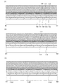
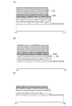
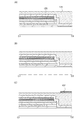
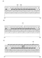
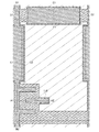
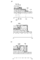
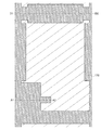
なお、図16乃至図20には本実施の形態に係る薄膜トランジスタの上面図を示し、図20は画素電極まで形成した完成図である。図1乃至図3は、図16乃至図20に示すA1−A2における断面図である。図4乃至図6は、図16乃至図20に示すB1−B2における断面図である。図7乃至図9は、図16乃至図20に示すC1−C2における断面図である。図10乃至図12は、図16乃至図20に示すD1−D2における断面図である。図13乃至図15は、図16乃至図20に示すE1−E2における断面図である。 16 to 20 show top views of the thin film transistor according to this embodiment mode, and FIG. 20 is a completed view including pixel electrodes. 1 to 3 are cross-sectional views taken along line A1-A2 shown in FIGS. 4 to 6 are cross-sectional views taken along B1-B2 shown in FIGS. 7 to 9 are cross-sectional views taken along line C1-C2 shown in FIGS. 10 to 12 are cross-sectional views taken along D1-D2 shown in FIGS. FIGS. 13 to 15 are cross-sectional views taken along E1-E2 shown in FIGS.
まず、基板100上に、第1の絶縁膜101、第1の導電膜102、第2の絶縁膜104、半導体膜106、不純物半導体膜108及び第2の導電膜110を形成する。これらの膜は、単層で形成してもよいし、複数の膜を積層した積層膜であってもよい。
First, the first insulating
基板100は、絶縁性基板である。表示装置に適用する場合には、基板100としては、ガラス基板又は石英基板を用いることができる。本実施の形態においては、ガラス基板を用いる。
The
第1の絶縁膜101は、絶縁性材料により形成する。第1の絶縁膜101は、例えば、酸化シリコン膜、窒化シリコン膜、酸化窒化シリコン膜又は窒化酸化シリコン膜等を用いて形成することができる。ただし、後の工程(第2の絶縁膜104の形成等)に耐えうる程度の耐熱性は必要である。また、後の工程(第2の導電膜110のエッチング等)で食刻又は腐食されない材料を選択する。
The first
基板100としてガラス基板を用いる場合には、第1の絶縁膜101には窒化シリコン膜又は窒化酸化シリコン膜を用いることが好ましい。第1の絶縁膜101が窒素を含むことで、ガラス基板100中の不純物金属元素が後に形成される半導体層に侵入することを効果的に防ぐことができるためである。更には、第1の絶縁膜101がハロゲン(フッ素、塩素又は臭素)を含むことが好ましい。第1の絶縁膜101にハロゲンを含ませることで、ガラス基板100中の不純物金属元素が半導体層に侵入することをより効果的に防ぐことができるためである。第1の絶縁膜101にハロゲンを含ませるには、第1の絶縁膜101を形成する際に用いるガスに、ハロゲンガス又はハロゲン元素を含むガスを含ませればよい。
In the case where a glass substrate is used as the
なお、第1の絶縁膜101は、例えばCVD法(熱CVD法又はプラズマCVD法等を含む)又はスパッタリング法等により形成することができるが、特定の方法に限定されるものではない。また、第1の絶縁膜101は、単層で形成しても良いし、複数の層を積層して形成しても良い。
Note that the first insulating
また、第1の絶縁膜101は、下地膜又は下地絶縁膜とも呼ぶことができる。
The first
第1の導電膜102は、導電性材料により形成する。第1の導電膜102は、例えばチタン、モリブデン、クロム、タンタル、タングステン、アルミニウム、銅、ネオジム、ニオブ若しくはスカンジウム等の金属又はこれらを主成分とする合金等の導電性材料を用いて形成することができる。ただし、後の工程(第2の絶縁膜104の形成等)に耐えうる程度の耐熱性は必要であり、後の工程(第2の導電膜110のエッチング等)で食刻又は腐食されない材料を選択することを要する。この限りにおいて、第1の導電膜102は特定の材料に限定されるものではない。
The first
なお、第1の導電膜102は、例えばスパッタリング法又はCVD法(熱CVD法又はプラズマCVD法等を含む)等により形成することができる。ただし、特定の方法に限定されるものではない。
Note that the first
第2の絶縁膜104は、絶縁性材料により形成する。第2の絶縁膜104は、例えば、酸化シリコン膜、窒化シリコン膜、酸化窒化シリコン膜又は窒化酸化シリコン膜等を用いて形成することができる。ただし、第1の導電膜102と同様に耐熱性が必要であり、後の工程で食刻又は腐食されない材料を選択することを要する。この限りにおいて、第2の絶縁膜104は特定の材料に限定されるものではない。
The second
なお、第2の絶縁膜104は、例えばCVD法(熱CVD法又はプラズマCVD法等を含む)又はスパッタリング法等により形成することができるが、特定の方法に限定されるものではない。
Note that the second
また、第2の絶縁膜104は、ゲート絶縁膜として機能するものである。
The second
半導体膜106は、半導体材料により形成する。半導体膜106は、例えば、シランガスにより形成される非晶質シリコン等を用いて形成することができる。ただし、第1の導電膜102等と同様に、耐熱性が必要であり、後の工程で食刻又は腐食されない材料を選択することを要する。この限りにおいて、半導体膜106は特定の材料に限定されるものではない。従って、ゲルマニウム等を用いても良い。なお、半導体膜106の結晶性についても特に限定されない。
The
なお、半導体膜106は、例えばCVD法(熱CVD法又はプラズマCVD法等を含む)又はスパッタリング法等により形成することができる。ただし、特定の方法に限定されるものではない。
Note that the
不純物半導体膜108は、一導電性を付与する不純物元素を含む半導体膜であり、一導電性を付与する不純物元素が添加された半導体形成のための材料ガス等により形成される。例えば、フォスフィン(化学式:PH3)又はジボラン(化学式:B2H6)を含むシランガスにより形成される、リン又はボロンを含むシリコン膜である。ただし、第1の導電膜102等と同様に、耐熱性が必要であり、後の工程で食刻又は腐食されない材料を選択することを要する。この限りにおいて、不純物半導体膜108は、特定の材料に限定されるものではない。なお、不純物半導体膜108の結晶性についても特に限定されるものではない。
The
なお、n型の薄膜トランジスタを作製する場合には、添加する一導電性を付与する不純物元素として、リン又はヒ素等を用いればよい。すなわち、形成に用いるシランガスにはフォスフィン又はアルシン(化学式:AsH3)等を所望の濃度で含ませればよい。または、p型の薄膜トランジスタを作製する場合には、一導電性を付与する不純物元素として、ボロン等を添加すればよい。すなわち、形成に用いるシランガスにはジボラン等を所望の濃度で含ませればよい。また、半導体膜106により形成される半導体層の一部に、ドーピング等によりソース電極及びドレイン電極層とオーミック接触可能な領域を設ける場合などには、不純物半導体膜108を設ける必要がない。
Note that in the case of manufacturing an n-type thin film transistor, phosphorus, arsenic, or the like may be used as an impurity element imparting one conductivity to be added. That is, phosphine or arsine (chemical formula: AsH 3 ) or the like may be included in the silane gas used for formation at a desired concentration. Alternatively, when a p-type thin film transistor is manufactured, boron or the like may be added as an impurity element imparting one conductivity. That is, the silane gas used for formation may contain diborane or the like at a desired concentration. In addition, when a region that can make ohmic contact with the source and drain electrode layers is provided in part of the semiconductor layer formed of the
なお、不純物半導体膜108は、例えばCVD法(熱CVD法又はプラズマCVD法等を含む)等により形成することができる。ただし、特定の方法に限定されるものではない。
Note that the
第2の導電膜110は、導電性材料(第1の導電膜102として列挙した材料等)であって、第1の導電膜102とは異なる材料により形成する。ここで、「異なる材料」とは、主成分が異なる材料をいう。具体的には、後に説明する第2のエッチングによりエッチングされにくい材料を選択すればよい。また、第1の導電膜102等と同様に、耐熱性が必要であり、後の工程で食刻又は腐食されない材料を選択することを要する。従って、この限りにおいて、第2の導電膜110は特定の材料に限定されるものではない。
The second
なお、第2の導電膜110は、例えばスパッタリング法又はCVD法(熱CVD法又はプラズマCVD法等を含む)等により形成することができる。ただし、特定の方法に限定されるものではない。
Note that the second
なお、上記説明した第1の導電膜102、第2の絶縁膜104、半導体膜106、不純物半導体膜108及び第2の導電膜110に対して求められる耐熱性は、第1の導電膜102が最も高く、以下前記した順に続き、第2の導電膜110が最も低い。例えば、半導体膜106が水素を含む非晶質半導体膜である場合には、約300℃以上とすることで半導体膜106中の水素が脱離し、電気的特性が変化する。そのため、例えば半導体膜106を形成した後の工程では300℃を超えない温度とすることが好ましい。
Note that the heat resistance required for the first
次に、第2の導電膜110上に第1のレジストマスク112を形成する(図1(A)、図4(A)、図7(A)、図10(A)、図13(A)を参照)。第1のレジストマスク112は凹部又は凸部を有するレジストマスクである。換言すると、厚さの異なる複数の領域(ここでは、二の領域)からなるレジストマスクともいうことができる。第1のレジストマスク112において、厚い領域を第1のレジストマスク112の凸部と呼び、薄い領域を第1のレジストマスク112の凹部と呼ぶこととする。
Next, a first resist
第1のレジストマスク112において、ソース電極及びドレイン電極層120が形成される領域には凸部が形成され、ソース電極及びドレイン電極層120を有さず半導体層が露出して形成される領域には凹部が形成される。
In the first resist
第1のレジストマスク112は、多階調マスクを用いることで形成することができる。ここで、多階調マスクについて図25を参照して以下に説明する。
The first resist
多階調マスクとは、多段階の光量で露光を行うことが可能なマスクであり、代表的には、露光領域、半露光領域及び未露光領域の3段階の光量で露光を行うものをいう。多階調マスクを用いることで、一度の露光及び現像工程によって、複数(代表的には二種類)の厚さを有するレジストマスクを形成することができる。そのため、多階調マスクを用いることで、フォトマスクの枚数を削減することができる。 A multi-tone mask is a mask that can be exposed with a multi-level light quantity, and typically represents an exposure that is performed with a 3-level light quantity of an exposed area, a half-exposed area, and an unexposed area. . By using a multi-tone mask, a resist mask having a plurality of thicknesses (typically two types) can be formed by one exposure and development process. Therefore, the number of photomasks can be reduced by using a multi-tone mask.
図25(A−1)及び図25(B−1)は、代表的な多階調マスクの断面図を示す。図25(A−1)にはグレートーンマスク140を示し、図25(B−1)にはハーフトーンマスク145を示す。
25A-1 and 25B-1 are cross-sectional views of typical multi-tone masks. FIG. 25A-1 shows a
図25(A−1)に示すグレートーンマスク140は、透光性を有する基板141上に遮光膜により形成された遮光部142、及び遮光膜のパターンにより設けられた回折格子部143で構成されている。
A gray-
回折格子部143は、露光に用いる光の解像度限界以下の間隔で設けられたスリット、ドット又はメッシュ等を有することで、光の透過量を制御する。なお、回折格子部143に設けられるスリット、ドット又はメッシュは周期的なものであってもよいし、非周期的なものであってもよい。
The
透光性を有する基板141としては、石英等を用いることができる。遮光部142及び回折格子部143を構成する遮光膜は、金属膜を用いて形成すればよく、好ましくはクロム又は酸化クロム等により設けられる。
As the
グレートーンマスク140に露光するための光を照射した場合、図25(A−2)に示すように、遮光部142に重畳する領域における透光率は0%となり、遮光部142又は回折格子部143が設けられていない領域における透光率は100%となる。また、回折格子部143における透光率は、概ね10〜70%の範囲であり、回折格子のスリット、ドット又はメッシュ等の間隔により調整可能である。
When the
図25(B−1)に示すハーフトーンマスク145は、透光性を有する基板146上に半透光膜により形成された半透光部147、及び遮光膜により形成された遮光部148で構成されている。
A
半透光部147は、MoSiN、MoSi、MoSiO、MoSiON、CrSi等の膜を用いて形成することができる。遮光部148は、グレートーンマスクの遮光膜と同様の金属膜を用いて形成すればよく、好ましくはクロム又は酸化クロム等により設けられる。
The
ハーフトーンマスク145に露光するための光を照射した場合、図25(B−2)に示すように、遮光部148に重畳する領域における透光率は0%となり、遮光部148又は半透光部147が設けられていない領域における透光率は100%となる。また、半透光部147における透光率は、概ね10〜70%の範囲であり、形成する材料の種類又は形成する膜厚等により、調整可能である。
When light for exposure is applied to the
多階調マスクを用いて露光して現像を行うことで、膜厚の異なる領域を有する第1のレジストマスク112を形成することができる。
By performing exposure and development using a multi-tone mask, the first resist
ただし、本実施形態はこれに限定されず、多階調マスクを用いることなく第1のレジストマスクを形成してもよい。また、上記したように、第1のレジストマスクが凹部又は凸部を有さないレジストマスクであってもよい。 However, the present embodiment is not limited to this, and the first resist mask may be formed without using a multi-tone mask. Further, as described above, the first resist mask may be a resist mask that does not have a concave portion or a convex portion.
次に、第1のレジストマスク112を用いて第1のエッチングを行う。すなわち、第1の導電膜102、第2の絶縁膜104、半導体膜106、不純物半導体膜108及び第2の導電膜110をエッチングによりパターニングし、薄膜積層体114及びエッチングされた第1の導電膜113を形成する(図1(B)、図4(B)、図7(B)、図10(B)、図13(B)、図16を参照)。このとき、第1の絶縁膜101の上部もエッチングされ、エッチングされた第1の絶縁膜115が形成される。このエッチング工程を第1のエッチングとよぶ。第1のエッチングは、ドライエッチング又はウエットエッチングを用いればよいが、異方性の高いエッチング法(物理的エッチング)により行うことが好ましい。第1のエッチングに異方性の高いエッチング法を用いることで、パターンの加工精度を向上させることができる。なお、第1のエッチングをドライエッチングにより行う場合には一の工程にて行うことが可能であるが、第1のエッチングをウエットエッチングにより行う場合には複数の工程により第1のエッチングを行うと良い。ウエットエッチングでは、被エッチング膜の種類によってエッチングレートが異なり、従って全ての膜を一の工程にてエッチングすることが困難だからである。本実施の形態では、第1のエッチングを一の工程により行う場合にはドライエッチングを用い、複数の工程により行う場合には少なくとも第1の導電膜102のエッチングにドライエッチングを用いる。すなわち、第1の導電膜102はドライエッチングで加工してエッチングされた第1の導電膜113を形成すると良い。
Next, first etching is performed using the first resist
下地絶縁膜として機能するエッチングされた第1の絶縁膜115を有することで、第1のエッチングにおいて基板100の食刻を防ぐことができる。そのため、基板100中に含まれる不純物金属元素の半導体層への付着及び半導体層内部への侵入を防ぐことができる。
With the etched first insulating
なお、第1のエッチングは、例えば3段階のドライエッチングにより行えばよい。まず、Cl2ガスとCF4ガスとO2ガスの混合ガス中でエッチングを行い、次に、Cl2ガスのみを用いてエッチングを行い、最後に、CHF3ガスのみを用いてエッチングを行えばよい。 Note that the first etching may be performed by, for example, three-stage dry etching. First, etching is performed in a mixed gas of Cl 2 gas, CF 4 gas and O 2 gas, then etching is performed using only Cl 2 gas, and finally etching is performed using only CHF 3 gas. Good.
次に、第1のレジストマスク112を用いて第2のエッチングを行う。すなわち、エッチングされた第1の導電膜113をさらにエッチングによりパターニングし、ゲート電極層116を形成する(図1(C)、図4(C)、図7(C)、図10(C)、図13(C)、図17を参照)。このエッチング工程を第2のエッチングとよぶ。
Next, second etching is performed using the first resist
なお、ゲート電極層116は、薄膜トランジスタのゲート電極、ゲート配線、容量素子の一方の電極、容量配線及び支持部を構成している。ゲート電極層116Aと表記する場合には、ゲート配線と薄膜トランジスタのゲート電極を構成するゲート電極層を指す。ゲート電極層116B又はゲート電極層116Dと表記する場合には支持部を構成するゲート電極層を指す。ゲート電極層116Cと表記する場合には容量配線と容量素子の一方の電極を構成するゲート電極層を指す。そして、これらを総括してゲート電極層116と呼ぶ。
Note that the
第2のエッチングは、第1の導電膜102により形成されるゲート電極層116の側面が、薄膜積層体114の側面より内側に形成されるエッチング条件により行う。換言すると、ゲート電極層116の側面が、薄膜積層体114の底面に接して形成されるようにエッチングを行う(図17乃至図20におけるA1−A2断面においてゲート電極層116の幅が薄膜積層体114の幅より小さくなるようにエッチングを行う)。更には、第2の導電膜110に対するエッチングレートが小さく、且つ第1の導電膜102に対するエッチングレートが大きい条件により行う。換言すると、第2の導電膜110に対する第1の導電膜102のエッチング選択比が大きい条件により行う。このような条件により第2のエッチングを行うことで、ゲート電極層116を形成することができる。
The second etching is performed under an etching condition in which the side surface of the
なお、ゲート電極層116の側面の形状は特に限定されない。例えば、テーパ形状であっても良い。ゲート電極層116の側面の形状は、第2のエッチングにおいて用いる薬液等の条件によって決められるものである。
Note that the shape of the side surface of the
ここで、「第2の導電膜110に対するエッチングレートが小さく、且つ第1の導電膜102に対するエッチングレートが大きい条件」、又は「第2の導電膜110に対する第1の導電膜102のエッチング選択比が大きい条件」とは、以下の第1の要件及び第2の要件を満たすものをいう。
Here, “a condition in which the etching rate with respect to the second
第1の要件は、ゲート電極層116が必要な箇所に残存することである。ゲート電極層116の必要な箇所とは、図17乃至図20に点線で示される領域をいう。すなわち、第2のエッチング後に、ゲート電極層116がゲート配線、容量配線及び支持部を構成するように残存することが必要である。ゲート電極層がゲート配線及び容量配線を構成するためには、これらの配線が断線しないように第2のエッチングを行う必要がある。図1及び図20に示されるように、薄膜積層体114の側面から間隔d1だけ内側にゲート電極層116の側面が形成されることが好ましく、間隔d1は実施者がレイアウトに従って適宜設定すればよい。
The first requirement is that the
第2の要件は、ゲート電極層116により構成されるゲート配線及び容量配線の最小幅d3、並びにソース電極及びドレイン電極層120Aにより構成されるソース配線の最小幅d2が適切なものとなることである(図20を参照)。第2のエッチングによりソース電極及びドレイン電極層120Aがエッチングされるとソース配線の最小幅d2が小さくなり、ソース配線の電流密度が過大となり、電気的特性が低下するためである。そのため、第2のエッチングは、第1の導電膜102のエッチングレートが過大にならず、且つ第2の導電膜110のエッチングレートが可能な限り小さい条件で行う。
The second requirement is that the minimum width d 3 of the gate wiring and the capacitor wiring constituted by the
また、ソース配線の最小幅d2は大きくすることが困難である。ソース配線の最小幅d2はソース配線と重畳する半導体層の最小幅d4により決まり、ソース配線の最小幅d2を大きくするためには半導体層の最小幅d4を大きくせねばならず、隣接するゲート配線と容量配線とを絶縁させることが困難になるためである。従って、半導体層の最小幅d4は、前記した間隔d1の概ね2倍よりも小さくする。換言すると、間隔d1は半導体層の最小幅d4の約半分よりも大きくする。 Further, it is difficult to minimum width d 2 of the source wiring is increased. The minimum width d 2 of the source wiring is determined by the minimum width d 4 of the semiconductor layer overlapping with the source wiring. In order to increase the minimum width d 2 of the source wiring, the minimum width d 4 of the semiconductor layer must be increased. This is because it becomes difficult to insulate the adjacent gate wiring from the capacitor wiring. Accordingly, the minimum width d 4 of the semiconductor layer is set to be smaller than about twice the distance d 1 described above. In other words, the distance d 1 is set to be larger than about half of the minimum width d 4 of the semiconductor layer.
なお、ソース配線と重畳する半導体層の幅を最小幅d4とする部分は、ゲート配線と、該ゲート配線と互いに隣接する容量配線との間に少なくとも一箇所あればよい。好ましくは、図20に示すように、ゲート配線に隣接する領域及び容量配線に隣接する領域の半導体層の幅を最小幅d4とすればよい。 A portion of the width of the semiconductor layer overlapping with the source wiring and the minimum width d 4 includes a gate line, it may be at least one place between the capacitor lines adjacent to each other with the gate wiring. Preferably, as shown in FIG. 20, the widths of the semiconductor layer in a region adjacent to the region and the capacitor wiring adjacent to the gate wiring may be the minimum width d 4.
なお、ソース電極及びドレイン電極層により形成される、画素電極層と接続される部分の電極の幅はソース配線の最小幅d2とすることが好ましい。 Incidentally, formed by the source electrode and the drain electrode layer, the width of the portion of the electrode connected to the pixel electrode layer is preferably set to the minimum width d 2 of the source wiring.
上記説明したように、サイドエッチングを伴う条件により第2のエッチングを行うことは非常に重要である。第2のエッチングが第1の導電膜102のサイドエッチングを伴うことによって、ゲート電極層116により構成される、隣接するゲート配線と容量配線とを絶縁させることができるためである(図17を参照)。
As described above, it is very important to perform the second etching under conditions involving side etching. This is because when the second etching is accompanied by side etching of the first
ここで、第2のエッチングは、サイドエッチングを伴うエッチングであるため、エッチングは概略等方的に進行する。上記説明したように、第1のエッチングにより第1の導電膜102を加工してエッチングされた第1の導電膜113を形成し、第2のエッチングによりゲート電極層116を形成することで、前記間隔d1を第1の導電膜102の厚さより小さくすることが可能になる。すなわち、前記間隔d1を第1の導電膜102の厚さに対して独立に設計することができ、画素構造のレイアウト設計の自由度が向上する。
Here, since the second etching is etching accompanied by side etching, the etching proceeds approximately isotropically. As described above, the first
ここで、サイドエッチングとは、被エッチング膜の厚さ方向(基板面に垂直な方向又は下地膜の面に垂直な方向)のみならず、厚さ方向に対して垂直な方向(基板面に平行な方向又は下地膜の面に平行な方向)にも被エッチング膜が削られるエッチングをいう。サイドエッチングされた被エッチング膜の端部は、被エッチング膜に対するエッチングガス又はエッチングに用いる薬液のエッチングレートによって様々な形状となるように形成されるが、端部が曲面となるように形成されることが多い。 Here, the side etching means not only the thickness direction of the film to be etched (the direction perpendicular to the substrate surface or the direction perpendicular to the surface of the base film) but also the direction perpendicular to the thickness direction (parallel to the substrate surface). Etching in which the film to be etched is also cut in a certain direction or a direction parallel to the surface of the base film). The end portion of the etched film subjected to side etching is formed to have various shapes depending on the etching rate of the etching gas for the etched film or the chemical solution used for etching, but the end portion is formed to be a curved surface. There are many cases.
なお、図17に示すように、第1のエッチングにより形成される薄膜積層体114は、ゲート電極層116B及びゲート電極層116Dにより構成される支持部に接する部分では細くなるように設計される(図17において両矢印で示す部分を参照)。このような構造とすることで、第2のエッチングによりゲート電極層116Aと、ゲート電極層116B又はゲート電極層116Dとを分断して絶縁させることができる。
Note that, as shown in FIG. 17, the
なお、図17に示すゲート電極層116B及びゲート電極層116Dは、薄膜積層体114を支える支持部として機能する。支持部を有することで、ゲート電極層より上に形成されるゲート絶縁膜等の膜剥がれを防止することができる。更には支持部を設けることで、第2のエッチングによりゲート電極層116に接して形成される、空洞の領域が必要以上に広くなることを防止できる。なお、支持部を設けることで、薄膜積層体114が自重によって破壊され、又は破損することをも防止することができ、歩留まりが向上するため好ましい。ただし、本実施の形態は支持部を有する形態に限定されず、支持部を設けなくとも良い。支持部を有しない形態の上面図(図20に対応)の一例を図21に示す。
Note that the
以上説明したように、第2のエッチングは、ウエットエッチングにより行うことが好ましい。 As described above, the second etching is preferably performed by wet etching.
第2のエッチングをウエットエッチングによって行う場合、第1の導電膜102をアルミニウム又はモリブデンにより形成し、第2の導電膜110をチタン又はタングステンにより形成し、エッチングには硝酸、酢酸及びリン酸を含む薬液を用いればよい。または、第1の導電膜102をモリブデンにより形成し、第2の導電膜110をチタン、アルミニウム又はタングステンにより形成し、エッチングには過酸化水素水を含む薬液を用いればよい。
In the case where the second etching is performed by wet etching, the first
第2のエッチングをウエットエッチングによって行う場合、最も好ましくは、第1の導電膜102としてネオジムを添加したアルミニウム上にモリブデンを形成した積層膜を形成し、第2の導電膜110をタングステンにより形成し、エッチングには硝酸を2%、酢酸を10%、リン酸を72%含む薬液を用いる。このような組成の薬液を用いることで、第2の導電膜110がエッチングされることなく、エッチングされた第1の導電膜113がさらにエッチングされる。なお、第1の導電膜102に添加したネオジムは、アルミニウムの低抵抗化とヒロックの発生防止を目的として添加されたものである。
In the case where the second etching is performed by wet etching, most preferably, a laminated film in which molybdenum is formed over aluminum added with neodymium is formed as the first
なお、図17に示すように、上面から見たゲート電極層116は角(例えば、角151)を有する。これは、ゲート電極層116を形成する第2のエッチングが概略等方的であるために、ゲート電極層116の側面と薄膜積層体114の側面との間隔d1が概略等しくなるようにエッチングされるためである。
As shown in FIG. 17, the
次に、第1のレジストマスク112を後退させる。例えば、第1のレジストマスク112を薄くする。そして第2の導電膜110を露出させつつ、第2のレジストマスク118を形成する。第1のレジストマスク112を後退させて、第2のレジストマスク118を形成する手段としては、例えば酸素プラズマを用いたアッシングが挙げられる。しかし、第1のレジストマスク112を後退させて第2のレジストマスク118を形成する手段はこれに限定されるものではない。なお、ここでは第2のエッチングの後に第2のレジストマスク118を形成する場合について説明したが、本実施の形態はこれに限定されず、第2のレジストマスク118を形成した後に第2のエッチングを行ってもよい。
Next, the first resist
次に、第2のレジストマスク118を用いて、薄膜積層体114における第2の導電膜110をエッチングし、ソース電極及びドレイン電極層120を形成する(図2(D)、図5(D)、図8(D)、図11(D)、図14(D)、図18を参照)。ここでエッチング条件は、第2の導電膜110以外の膜に対する食刻及び腐食が生じず、又は生じ難い条件を選択する。特に、ゲート電極層116の食刻及び腐食が生じず、又は生じ難い条件により行うことが重要である。
Next, the second
なお、ソース電極及びドレイン電極層120は、薄膜トランジスタのソース電極若しくはドレイン電極、ソース配線、薄膜トランジスタと画素電極とを接続する電極、及び容量素子の他方の電極を構成している。「ソース電極及びドレイン電極層120A」又は「ソース電極及びドレイン電極層120C」と表記する場合には、薄膜トランジスタのソース電極及びドレイン電極の一方、及びソース配線を構成する電極層を指す。「ソース電極及びドレイン電極層120B」と表記する場合には、薄膜トランジスタのソース電極及びドレイン電極の他方、及び薄膜トランジスタと画素電極とを接続する電極を構成する電極層を指す。「ソース電極及びドレイン電極層120D」と表記する場合には、容量素子の他方の電極を構成する電極層を指す。そして、これらを総括して「ソース電極及びドレイン電極層120」と呼ぶ。
Note that the source and drain electrode layers 120 constitute a source electrode or a drain electrode of a thin film transistor, a source wiring, an electrode for connecting the thin film transistor and the pixel electrode, and the other electrode of the capacitor. In the case of “source electrode and
なお、薄膜積層体114における第2の導電膜110のエッチングは、ウエットエッチング又はドライエッチングのどちらを用いても良い。
Note that either wet etching or dry etching may be used for etching the second
続いて、薄膜積層体114における不純物半導体膜108及び半導体膜106の上部(バックチャネル部)をエッチングして、ソース領域及びドレイン領域122を形成する(図2(E)、図5(E)、図8(E)、図11(E)、図14(E)、図19を参照)。ここでエッチング条件は、不純物半導体膜108及び半導体膜106以外の膜に対する食刻及び腐食が生じず、又は生じ難い条件を選択する。特に、ゲート電極層116の食刻及び腐食が生じず、又は生じ難い条件により行うことが重要である。
Subsequently, the
なお、薄膜積層体114における不純物半導体膜108及び半導体膜106の上部(バックチャネル部)のエッチングはドライエッチング又はウエットエッチングにより行うことができる。
Note that etching of the
その後、第2のレジストマスク118を除去し(図2(F)、図5(F)、図8(F)、図11(F)、図14(F)を参照)、薄膜トランジスタが完成する(図2(F)を参照)。上記説明したように、薄膜トランジスタを1枚のフォトマスク(多階調マスク)により作製することができる。
After that, the second resist
なお、上記の図2(D)及び図2(E)を参照して説明した工程を一括して第3のエッチングとよぶ。第3のエッチングは、上記説明したように、複数の段階に分けて行っても良いし、一括して行っても良い。 Note that the steps described with reference to FIGS. 2D and 2E are collectively referred to as third etching. As described above, the third etching may be performed in a plurality of stages or collectively.
以上のように形成した薄膜トランジスタを覆って第3の絶縁膜を形成する。ここで、第3の絶縁膜は、第1の保護膜126のみで形成しても良いが、好ましくは第1の保護膜126と第2の保護膜128により形成する(図3(G)、図6(G)、図9(G)、図12(G)、図15(G)を参照)。第1の保護膜126は、第2の絶縁膜104と同様に形成すればよい。
A third insulating film is formed to cover the thin film transistor formed as described above. Here, the third insulating film may be formed using only the first
第2の保護膜128は、表面が概略平坦になる方法により形成する。第2の保護膜128の表面を概略平坦にすることで、第2の保護膜128上に形成される画素電極層132の断切れ等を防止することができるためである。従って、ここで「概略平坦」とは、上記目的を達成しうる程度のものであればよく、高い平坦性が要求されるわけではない。
The second
なお、第2の保護膜128は、例えば、感光性ポリイミド、アクリル又はエポキシ樹脂等を用いて、スピンコーティング法等により形成することができる。ただし、これらの材料又は形成方法に限定されるものではない。
Note that the second
次に、第3の絶縁膜に第1の開口部130及び第2の開口部131を形成する(図3(H)、図6(H)、図9(H)、図12(H)、図15(H)を参照)。第1の開口部130及び第2の開口部131は、ソース電極及びドレイン電極層120の少なくとも表面に達するように形成する。第1の開口部130及び第2の開口部131の形成方法は、特定の方法に限定されず、第1の開口部130の径等に応じて実施者が適宜選択すればよい。例えば、フォトリソグラフィ法によりドライエッチングを行うことで第1の開口部130及び第2の開口部131を形成することができる。
Next, the
なお、フォトリソグラフィ法によって開口部を形成することで、フォトマスクを1枚使用することになる。 Note that one photomask is used by forming the opening by photolithography.
次に、第3の絶縁膜上に画素電極層132を形成する(図3(I)、図6(I)、図9(I)、図12(I)、図15(I)、図20を参照)。画素電極層132は、開口部を介してソース電極及びドレイン電極層120に接続されるように形成する。具体的には、画素電極層132は、第1の開口部130を介してソース電極及びドレイン電極層120Bに接続され、第2の開口部131を介してソース電極及びドレイン電極層120Dに接続されるように形成される。画素電極層132は、透光性を有する導電性材料により形成することが好ましい。ここで、透光性を有する導電性材料としては、インジウム錫酸化物(以下、ITOという)、酸化タングステンを含むインジウム酸化物、酸化タングステンを含むインジウム亜鉛酸化物、酸化チタンを含むインジウム酸化物、酸化チタンを含むインジウム錫酸化物、インジウム亜鉛酸化物、又は酸化シリコンを添加したインジウム錫酸化物等が挙げられる。透光性を有する導電性材料の膜の形成はスパッタリング法又はCVD法等により行えばよいが、特定の方法に限定されるものではない。また、画素電極層132についても単層で形成しても良いし、複数の膜を積層した積層膜としてもよい。
Next, the
なお、本実施の形態においては、画素電極層132のみに透光性を有する導電性材料を用いたが、本実施の形態はこれに限定されない。第1の導電膜102及び第2の導電膜110の材料として、透光性を有する導電性材料を用いることもできる。
Note that in this embodiment mode, a light-transmitting conductive material is used only for the
なお、フォトリソグラフィ法によって画素電極層132を形成することで、フォトマスクを1枚使用することになる。
Note that a single photomask is used by forming the
以上説明したように、本実施の形態に係るアクティブマトリクス基板の作製(所謂アレイ工程)が完了する。本実施の形態にて説明したように、サイドエッチングを利用してゲート電極層を形成し、更には多階調マスクを用いてソース電極及びドレイン電極層を形成することで、1枚のマスクによる薄膜トランジスタの作製が可能となる。 As described above, the production of the active matrix substrate according to the present embodiment (so-called array process) is completed. As described in this embodiment mode, a gate electrode layer is formed using side etching, and further, a source electrode and a drain electrode layer are formed using a multi-tone mask, so that a single mask is used. A thin film transistor can be manufactured.
上記のように作製した薄膜トランジスタは、下地絶縁膜上にゲート電極層を有し、前記ゲート電極層上にゲート絶縁膜を有し、前記ゲート絶縁膜上に半導体層を有し、前記半導体層上にソース領域及びドレイン領域を有する不純物半導体層を有し、前記ソース領域及びドレイン領域上にソース電極及びドレイン電極層を有し、前記ゲート電極層の側面に接して空洞を有する構造となる(図3(I)を参照)。このような薄膜トランジスタはゲート電極層の側面に接して空洞を有するため、ゲート電極層端部におけるリーク電流の小さいものとなる。更には、下地絶縁膜を有することで、基板としてガラス基板を用いる場合に、ガラス基板中の不純物金属元素が半導体層中に侵入することを防ぐことができる。そのため、電気的特性が良好(例えばオフ電流が低い等)であり、基板面内における電気的特性のばらつきが小さい。 The thin film transistor manufactured as described above includes a gate electrode layer on a base insulating film, a gate insulating film on the gate electrode layer, a semiconductor layer on the gate insulating film, and a semiconductor layer on the semiconductor layer. The semiconductor device includes an impurity semiconductor layer having a source region and a drain region, a source electrode and a drain electrode layer on the source region and the drain region, and a cavity in contact with a side surface of the gate electrode layer (see FIG. 3 (I)). Since such a thin film transistor has a cavity in contact with the side surface of the gate electrode layer, the leakage current at the end portion of the gate electrode layer is small. Further, by including the base insulating film, when a glass substrate is used as the substrate, the impurity metal element in the glass substrate can be prevented from entering the semiconductor layer. Therefore, the electrical characteristics are good (for example, the off current is low), and the variation in the electrical characteristics in the substrate surface is small.
ここで、上記の工程により作製したアクティブマトリクス基板の端子接続部について図22乃至図24を参照して説明する。 Here, a terminal connection portion of the active matrix substrate manufactured by the above steps will be described with reference to FIGS.
図22乃至図24は、上記工程により作製した、アクティブマトリクス基板におけるゲート配線側の端子接続部及びソース配線側の端子接続部の上面図と断面図を示す。 22 to 24 are a top view and a cross-sectional view of the terminal connection portion on the gate wiring side and the terminal connection portion on the source wiring side in the active matrix substrate manufactured by the above process.
図22は、ゲート配線側の端子接続部及びソース配線側の端子接続部における、画素部から延伸したゲート配線及びソース配線の上面図を示す。 FIG. 22 is a top view of the gate wiring and the source wiring extended from the pixel portion in the terminal connection portion on the gate wiring side and the terminal connection portion on the source wiring side.
図23は、図22のX1−X2における断面図を示す。すなわち、図23は、ゲート配線側の端子接続部における断面図を示す。図23では、ゲート電極層116が露出されている。このゲート電極層116が露出された領域に、端子部が接続される。
FIG. 23 is a cross-sectional view taken along X1-X2 in FIG. That is, FIG. 23 shows a cross-sectional view of the terminal connection portion on the gate wiring side. In FIG. 23, the
図24は、ソース配線側の端子接続部における断面図を示す。図24において、ゲート電極層116と、ソース電極及びドレイン電極層120は画素電極層132を介して接続されている。図24にはゲート電極層116と、ソース電極及びドレイン電極層120の様々な接続形態を示している。本実施の形態の表示装置の発明における端子接続部には、これらのいずれを用いても良いし、図24に示すもの以外の接続形態を用いても良い。ソース電極及びドレイン電極層120をゲート電極層116に接続させることで、端子の接続部の高さを概ね等しくすることができる。
FIG. 24 is a cross-sectional view of the terminal connection portion on the source wiring side. In FIG. 24, the
図24(A)では、第1の保護膜126及び第2の保護膜128の端部がエッチング等により除去され、ゲート電極層116と、ソース電極及びドレイン電極層120とが露出され、この露出された領域に画素電極層132を形成することで電気的な接続を実現することができる。図24(A)は、図22のY1−Y2における断面図に相当する。
In FIG. 24A, end portions of the first
なお、ゲート電極層116と、ソース電極及びドレイン電極層120とが露出された領域の形成は、第1の開口部130及び第2の開口部131の形成と同時に行うことができる。
Note that the formation of the region where the
図24(B)では、第1の保護膜126及び第2の保護膜128に第3の開口部160Aが設けられ、第1の保護膜126及び第2の保護膜128の端部がエッチング等により除去されることで、ゲート電極層116と、ソース電極及びドレイン電極層120とが露出され、この露出された領域に画素電極層132を形成することで電気的な接続を実現している。
In FIG. 24B, a
なお、第3の開口部160Aの形成、及びゲート電極層116が露出された領域の形成は、第1の開口部130及び第2の開口部131の形成と同時に行うことができる。
Note that the formation of the
図24(C)では、第1の保護膜126及び第2の保護膜128に第3の開口部160B及び第4の開口部161が設けられることで、ゲート電極層116と、ソース電極及びドレイン電極層120とが露出され、この露出された領域に画素電極層132を形成することで電気的な接続を実現している。ここで、図24(A)及び(B)と同様に、第1の保護膜126及び第2の保護膜128の端部はエッチング等により除去されているが、この領域は端子の接続部として用いられる。
24C, the
なお、第3の開口部160B及び第4の開口部161の形成、並びにゲート電極層116が露出された領域の形成は、第1の開口部130及び第2の開口部131の形成と同時に行うことができる。
Note that the formation of the
なお、開口部の数は図24に示す開口部の数に特に限定されない。一の端子に対して一の開口部を設けるのみならず、一の端子に対して複数の開口部を設けても良い。一の端子に対して複数の開口部を設けることで、開口部を形成するエッチング工程が不十分である等の理由で開口部が良好に形成されなかったとしても、他の開口部により電気的接続を実現することができる。更には、全ての開口部が問題なく形成された場合であっても、接触面積を広くすることができるため、コンタクト抵抗を低減することができ、好ましい。 Note that the number of openings is not particularly limited to the number of openings shown in FIG. In addition to providing one opening for one terminal, a plurality of openings may be provided for one terminal. By providing a plurality of openings for one terminal, even if the opening is not formed well due to an insufficient etching process for forming the opening, etc. Connection can be realized. Furthermore, even when all the openings are formed without any problem, the contact area can be increased, so that the contact resistance can be reduced, which is preferable.
次に、上記で説明した工程により作製した、表示装置のアクティブマトリクス基板を用いて液晶表示装置を作製する方法について説明する。すなわち、セル工程及びモジュール工程について説明する。ただし、本実施の形態に係る表示装置の作製方法において、セル工程及びモジュール工程は以下の説明に限定されない。 Next, a method for manufacturing a liquid crystal display device using the active matrix substrate of the display device manufactured through the above-described steps will be described. That is, the cell process and the module process will be described. However, in the method for manufacturing the display device according to this embodiment, the cell process and the module process are not limited to the following description.
セル工程では、上記した工程により作製したアクティブマトリクス基板と、これに対向する基板(以下、対向基板という)とを貼り合わせて液晶を注入する。まず、対向基板の作製方法について、以下に簡単に説明する。なお、特に説明しない場合であっても、対向基板上に形成する膜は単層でも良いし、積層して形成しても良い。 In the cell process, the active matrix substrate manufactured by the above-described process and a substrate facing the active matrix substrate (hereinafter referred to as a counter substrate) are bonded to each other and liquid crystal is injected. First, a method for manufacturing the counter substrate will be briefly described below. Note that a film formed over the counter substrate may be a single layer or a stacked layer even when not specifically described.
まず、基板上に遮光層を形成し、遮光層上に赤、緑、青のいずれかのカラーフィルター層を形成し、カラーフィルター層上に画素電極層を選択的に形成し、画素電極層上にリブを形成する。 First, a light shielding layer is formed on the substrate, a color filter layer of red, green, or blue is formed on the light shielding layer, and a pixel electrode layer is selectively formed on the color filter layer. Ribs are formed on the surface.
遮光層としては、遮光性を有する材料の膜を選択的に形成する。遮光性を有する材料としては、例えば、黒色樹脂(カーボンブラック)を含む有機樹脂を用いることができる。または、クロムを主成分とする材料膜の積層膜を用いても良い。クロムを主成分とする材料膜とは、クロム、酸化クロム又は窒化クロムをいう。遮光層に用いる材料は遮光性を有するものであれば特に限定されない。遮光性を有する材料の膜を選択的に形成するにはフォトリソグラフィ法等を用いる。 As the light shielding layer, a film of a material having a light shielding property is selectively formed. As the light-shielding material, for example, an organic resin containing a black resin (carbon black) can be used. Alternatively, a stacked film of material films containing chromium as a main component may be used. The material film containing chromium as a main component refers to chromium, chromium oxide, or chromium nitride. The material used for the light shielding layer is not particularly limited as long as it has light shielding properties. In order to selectively form a film of a light-shielding material, a photolithography method or the like is used.
カラーフィルター層は、バックライトから白色光が照射されると、赤、緑、青のいずれかの光のみを透過させることができる有機樹脂膜により選択的に形成すればよい。カラーフィルター層は、形成時に塗り分けを行うことで、選択的に形成することができる。カラーフィルターの配列は、ストライプ配列、デルタ配列又は正方配列を用いればよい。 The color filter layer may be selectively formed of an organic resin film that can transmit only one of red, green, and blue light when white light is irradiated from the backlight. The color filter layer can be selectively formed by separately coating at the time of formation. The arrangement of the color filters may be a stripe arrangement, a delta arrangement, or a square arrangement.
対向基板の画素電極層は、アクティブマトリクス基板が有する画素電極層132と同様に形成することができる。ただし、選択的に形成する必要がないため、対向基板の全面に形成すればよい。
The pixel electrode layer of the counter substrate can be formed in a manner similar to that of the
画素電極上に形成するリブは、視野角を拡げることを目的として形成される、パターン形成された有機樹脂膜である。特に必要のない場合には形成しなくてもよい。 The rib formed on the pixel electrode is a patterned organic resin film formed for the purpose of widening the viewing angle. If it is not particularly necessary, it may not be formed.
なお、対向基板の作製方法としては、他にも様々な態様が考えられる。例えば、カラーフィルター層を形成後、画素電極層の形成前にオーバーコート層を形成しても良い。オーバーコート層を形成することで画素電極の被形成面の平坦性を向上させることができるため、歩留まりが向上する。また、カラーフィルター層に含まれる材料の一部が液晶材料中に侵入することを防ぐことができる。オーバーコート層には、アクリル樹脂又はエポキシ樹脂をベースとした熱硬化性材料が用いられる。 Note that various other modes can be considered as a method for manufacturing the counter substrate. For example, an overcoat layer may be formed after the color filter layer is formed and before the pixel electrode layer is formed. By forming the overcoat layer, the flatness of the formation surface of the pixel electrode can be improved, so that the yield is improved. In addition, part of the material included in the color filter layer can be prevented from entering the liquid crystal material. For the overcoat layer, a thermosetting material based on acrylic resin or epoxy resin is used.
また、リブの形成前又は形成後にスペーサとしてポストスペーサ(柱状スペーサ)を形成しても良い。ポストスペーサとは、アクティブマトリクス基板と対向基板との間のギャップを一定に保つことを目的として、対向基板上に一定の間隔で形成する構造物をいう。ビーズスペーサ(球状スペーサ)を用いる場合には、ポストスペーサを形成しなくても良い。 Further, post spacers (columnar spacers) may be formed as spacers before or after the ribs are formed. The post spacer refers to a structure formed on the counter substrate at a constant interval for the purpose of maintaining a constant gap between the active matrix substrate and the counter substrate. When a bead spacer (spherical spacer) is used, the post spacer does not have to be formed.
次に、配向膜をアクティブマトリクス基板及び対向基板に形成する。配向膜の形成は、例えば、ポリイミド樹脂等を有機溶剤に溶かし、これを印刷法又はスピンコーティング法等により塗布し、有機溶媒を溜去した後基板を焼成することにより行う。形成される配向膜の膜厚は、一般に、50nm以上100nm以下程度とする。配向膜には、液晶分子がある一定のプレチルト角を持って配向するようにラビング処理を施す。ラビング処理は、例えば、ベルベット等の毛足の長い布により配向膜を擦ることで行う。 Next, an alignment film is formed on the active matrix substrate and the counter substrate. The alignment film is formed by, for example, dissolving a polyimide resin or the like in an organic solvent, applying the resin by a printing method or a spin coating method, and removing the organic solvent, and then baking the substrate. The thickness of the alignment film to be formed is generally about 50 nm to 100 nm. The alignment film is rubbed so that the liquid crystal molecules are aligned with a certain pretilt angle. The rubbing process is performed, for example, by rubbing the alignment film with a cloth having a long bristle such as velvet.
次に、アクティブマトリクス基板と、対向基板をシール材料により貼り合わせる。対向基板にポストスペーサが設けられていない場合には、ビーズスペーサを所望の領域に分散させて貼り合わせるとよい。 Next, the active matrix substrate and the counter substrate are bonded together with a sealing material. In the case where a post spacer is not provided on the counter substrate, the bead spacers may be dispersed and bonded to a desired region.
次に、貼り合わせられたアクティブマトリクス基板と、対向基板との間に、液晶材料を注入する。液晶材料を注入した後、注入口を紫外線硬化樹脂等で封止する。または、液晶材料をアクティブマトリクス基板と対向基板のいずれかの上に滴下した後に、これらの基板を貼り合わせても良い。 Next, a liquid crystal material is injected between the bonded active matrix substrate and the counter substrate. After injecting the liquid crystal material, the injection port is sealed with an ultraviolet curable resin or the like. Alternatively, after the liquid crystal material is dropped on either the active matrix substrate or the counter substrate, these substrates may be attached to each other.
次に、アクティブマトリクス基板と対向基板とを貼り合わせた液晶セルの両面に偏光板を貼り付けてセル工程が完了する。 Next, the polarizing plate is attached to both surfaces of the liquid crystal cell in which the active matrix substrate and the counter substrate are bonded to complete the cell process.
次に、モジュール工程として、端子部の入力端子(図24において、ゲート電極層116の露出された領域)にFPC(Flexible Printed Circuit)を接続する。FPCはポリイミド等の有機樹脂フィルム上に導電膜により配線が形成されており、異方性導電性ペースト(Anisotropic Conductive Paste。以下、ACPという)を介して入力端子と接続される。ACPは接着剤として機能するペーストと、金等がメッキされた数十〜数百μm径の導電性表面を有する粒子と、により構成される。ペースト中に混入された粒子が入力端子上の導電層と、FPCに形成された配線に接続された端子上の導電層と、に接触することで、電気的な接続を実現する。なお、FPCの接続後にアクティブマトリクス基板と対向基板に偏光板を貼り付けてもよい。以上のように、表示装置に用いる液晶パネルを作製することができる。
Next, as a module process, an FPC (Flexible Printed Circuit) is connected to an input terminal (an exposed region of the
以上のように、表示装置に用いる画素トランジスタを有するアクティブマトリクス基板を3枚のフォトマスクにより作製することができる。 As described above, an active matrix substrate including a pixel transistor used for a display device can be manufactured using three photomasks.
従って、薄膜トランジスタ及び表示装置の作製工程数を大幅に削減することができる。具体的には、上記の説明のように、1枚のフォトマスク(多階調マスク)を用いて薄膜トランジスタを作製することができる。また、3枚のフォトマスクを用いて画素トランジスタを有するアクティブマトリクス基板を作製することができる。従って、用いるフォトマスクの枚数が低減されることから、薄膜トランジスタ及び表示装置の作製工程数を大幅に削減することができる。 Accordingly, the number of manufacturing steps of the thin film transistor and the display device can be significantly reduced. Specifically, as described above, a thin film transistor can be manufactured using one photomask (multi-tone mask). In addition, an active matrix substrate having a pixel transistor can be manufactured using three photomasks. Accordingly, the number of photomasks to be used is reduced, so that the number of manufacturing steps of the thin film transistor and the display device can be significantly reduced.
また、裏面露光、レジストリフロー及びリフトオフ法等の複雑な工程を経ることなく、薄膜トランジスタの作製工程数を大幅に削減することができる。そのため、複雑な工程を経ることなく、表示装置の作製工程数を大幅に削減することができる。従って、歩留まりを低下させることなく、表示装置の作製工程数を大幅に削減することができる。 In addition, the number of thin film transistor manufacturing steps can be greatly reduced without going through complicated steps such as backside exposure, registry flow, and lift-off method. Therefore, the number of manufacturing steps of the display device can be significantly reduced without going through complicated steps. Therefore, the number of manufacturing steps of the display device can be significantly reduced without reducing the yield.
また、薄膜トランジスタの電気的特性を維持しつつ、薄膜トランジスタの作製工程を大幅に削減することができる。 In addition, the manufacturing process of the thin film transistor can be significantly reduced while maintaining the electrical characteristics of the thin film transistor.
更には、上記効果により、作製コストを大幅に削減することができる。 Furthermore, the manufacturing cost can be significantly reduced by the above effect.
また、第1のエッチングにより第1の導電膜102を加工するため、薄膜積層体114の側面とゲート電極層116の側面との間隔d1は第1の導電膜102の厚さに対して独立に設計することができ、画素構造のレイアウト設計の自由度が向上する。
In addition, since the first
また、基板として不純物金属元素を含むガラス基板を用いる場合であっても、該不純物金属元素が半導体層に付着し、半導体層内部へ侵入して薄膜トランジスタの電気的特性を低下させること(オフ電流が高くなること等)を防ぐことができる。そのため、電気的特性が良好な薄膜トランジスタを作製することができる。更には、作製される薄膜トランジスタの基板面内における特性のばらつきも小さくすることができる。そのため、表示装置の表示むらを小さくすることができる。 Further, even when a glass substrate containing an impurity metal element is used as the substrate, the impurity metal element adheres to the semiconductor layer and penetrates into the semiconductor layer, so that the electrical characteristics of the thin film transistor are deteriorated (off-state current is reduced). Etc.) can be prevented. Therefore, a thin film transistor with favorable electrical characteristics can be manufactured. Further, variation in characteristics of the thin film transistor to be manufactured in the substrate surface can be reduced. Therefore, display unevenness of the display device can be reduced.
なお、ゲート電極層端部に生じるリーク電流が小さい薄膜トランジスタを作製することができるため、コントラスト比が高く、表示品質が良好な表示装置を得ることができる。 Note that since a thin film transistor with a small leakage current generated at the end portion of the gate electrode layer can be manufactured, a display device with high contrast ratio and good display quality can be obtained.
なお、本実施の形態は、上記説明した画素構造に限定されず、様々な液晶表示装置に適用することができる。 Note that this embodiment is not limited to the pixel structure described above, and can be applied to various liquid crystal display devices.
(実施の形態2)
本実施の形態では、本発明の一態様である薄膜トランジスタの作製方法及び表示装置の作製方法であって、実施の形態1とは異なるものについて説明する。具体的には、多階調マスクを用いることなく、実施の形態1と同様に薄膜トランジスタを作製する方法について図26乃至図30を参照して説明する。
(Embodiment 2)
In this embodiment, a method for manufacturing a thin film transistor and a method for manufacturing a display device which are one embodiment of the present invention, which are different from those in
なお、図26は実施の形態1における図1及び図2に対応するものである。図27は実施の形態1における図10及び図11に対応するものである。図28、図29及び図30は実施の形態1における図16、図17及び図18に対応するものである。また、図28乃至図30に示すA1−A2における断面図が図26に相当し、図28乃至図30に示すD1−D2断面図が図27に相当する。 FIG. 26 corresponds to FIG. 1 and FIG. 2 in the first embodiment. FIG. 27 corresponds to FIG. 10 and FIG. 11 in the first embodiment. 28, 29 and 30 correspond to FIGS. 16, 17 and 18 in the first embodiment. A cross-sectional view taken along A1-A2 in FIGS. 28 to 30 corresponds to FIG. 26, and a D1-D2 cross-sectional view illustrated in FIGS. 28 to 30 corresponds to FIG.
まず、実施の形態1と同様に、基板100上に第1の絶縁膜101、第1の導電膜102、第2の絶縁膜104、半導体膜106、不純物半導体膜108及び第2の導電膜110を形成する(図26(A)及び図27(A)を参照)。これらに用いることのできる材料及びこれらの形成に適用することのできる方法は実施の形態1と同様である。なお、半導体膜106により形成される半導体層の一部に、ドーピング等によりソース電極及びドレイン電極層とオーミック接触可能な領域を設ける場合などには、不純物半導体膜108を設ける必要がない。
First, as in
次に、第2の導電膜110上に第1のレジストマスク170を形成する(図26(A)及び図27(A)を参照)。第1のレジストマスク170は、実施の形態1における第1のレジストマスク112とは異なるものであり、凹部が設けられておらず、全面が概略同一の厚さとなるように形成されている。すなわち、第1のレジストマスク170は多階調マスクを用いることなく形成することができる。
Next, a first resist
次に、第1のレジストマスク170を用いて第1のエッチングを行う。すなわち、第1の導電膜102、第2の絶縁膜104、半導体膜106、不純物半導体膜108及び第2の導電膜110をエッチングによりパターニングし、第1の導電膜102上に薄膜積層体114を形成する(図28を参照)。また、実施の形態1と同様に、第1のエッチングにより第1の絶縁膜101の上部もエッチングされ、エッチングされた第1の絶縁膜115が形成される。
Next, first etching is performed using the first resist
次に、実施の形態1と同様に第2のエッチングを行うことで、ゲート電極層116を形成する(図26(C)、図27(C)及び図29を参照)。
Next, second etching is performed in a manner similar to that in
ここで、第2のエッチングの条件は、実施の形態1における第2のエッチングと同様である。 Here, the conditions for the second etching are the same as those for the second etching in the first embodiment.
次に、薄膜積層体114上に第2のレジストマスク171を形成し、第2のレジストマスク171を用いてソース電極及びドレイン電極層120を形成する(図26(D)、図27(D)、図30参照)。エッチング条件等は、実施の形態1と同様である。また、その後の工程は実施の形態1と同様である。
Next, a second resist
なお、ここでは第2のエッチングの後に第2のレジストマスク171を形成する場合について説明したが、これに限定されず、第2のレジストマスク171を形成した後に第2のエッチングを行ってもよい。
Note that although the case where the second resist
以上、本実施の形態にて説明したように、多階調マスクを用いることなく薄膜トランジスタを作製することができる。ただし、使用するマスク数は、実施の形態1と比較すると1枚多いことになる。 As described above in this embodiment, a thin film transistor can be manufactured without using a multi-tone mask. However, the number of masks used is one more than that in the first embodiment.
なお、本実施の形態に係る薄膜トランジスタ及び表示装置の作製方法は、上記説明した点を除き、実施の形態1と同様である。そのため、実施の形態1に係る薄膜トランジスタ及び表示装置の作製方法と同様の効果を有することは勿論であるが、使用するマスクの数は1枚増加する。すなわち、本実施の形態によれば、2枚のフォトマスクを用いて薄膜トランジスタを作製することができる。また、4枚のフォトマスクを用いて画素トランジスタを有するアクティブマトリクス基板を作製することができる。従って、多階調マスクを用いない従来の手法と比較し、フォトマスクの枚数が低減されることから、薄膜トランジスタ及び表示装置の作製工程数を大幅に削減することができる。更には、高い歩留まりで製造することができ、コストを低く抑えることも可能である。
Note that a method for manufacturing the thin film transistor and the display device according to this embodiment is similar to that of
また、実施の形態1と同様に、薄膜トランジスタの電気的特性を維持しつつ、薄膜トランジスタの作製工程を大幅に削減することができる。
Further, as in
また、実施の形態1と同様に、第1のエッチングにより第1の導電膜102を加工するため、薄膜積層体114の側面とゲート電極層116の側面との間隔d1(図26(C)及び図29参照)は第1の導電膜102の厚さに対して独立に設計することができ、画素構造のレイアウト設計の自由度が向上する。
Similarly to
また、実施の形態1と同様に、基板として不純物金属元素を含むガラス基板を用いる場合であっても、該不純物金属元素が半導体層に付着し、半導体層内部へ侵入して薄膜トランジスタの電気的特性を低下させること(オフ電流が高くなること等)を防ぐことができる。そのため、電気的特性が良好な薄膜トランジスタを作製することができる。更には、作製される薄膜トランジスタの基板面内における特性のばらつきも小さくすることができる。そのため、表示装置の表示むらを小さくすることができる。
Further, as in
なお、本実施の形態の作製方法を適用して作製した薄膜トランジスタにおいても、絶縁膜上にゲート電極層を有し、前記ゲート電極層上にゲート絶縁膜を有し、前記ゲート絶縁膜上に半導体層を有し、前記半導体層上にソース領域及びドレイン領域を有する不純物半導体層を有し、前記ソース領域及びドレイン領域上にソース電極及びドレイン電極を有し、前記ゲート電極層の側面に接して空洞を有する構造となる。ゲート電極層の側面に接して空洞を有するように形成することで、ゲート電極層端部におけるリーク電流の小さい薄膜トランジスタを作製することができる。従って、コントラスト比が高く、表示品質が良好な表示装置を得ることができる。 Note that a thin film transistor manufactured using the manufacturing method of this embodiment also includes a gate electrode layer over an insulating film, a gate insulating film over the gate electrode layer, and a semiconductor over the gate insulating film. An impurity semiconductor layer having a source region and a drain region on the semiconductor layer, a source electrode and a drain electrode on the source region and the drain region, and in contact with a side surface of the gate electrode layer The structure has a cavity. By forming a cavity in contact with the side surface of the gate electrode layer, a thin film transistor with a small leakage current at the end portion of the gate electrode layer can be manufactured. Therefore, a display device with a high contrast ratio and good display quality can be obtained.
(実施の形態3)
本実施の形態では、薄膜トランジスタ及び該薄膜トランジスタがマトリクス状に配置されたEL表示装置を作製する方法の一例について、図31乃至図39,及び図43を参照して説明する。
(Embodiment 3)
In this embodiment, an example of a method for manufacturing a thin film transistor and an EL display device in which the thin film transistor is arranged in a matrix will be described with reference to FIGS.
薄膜トランジスタをスイッチング素子として用いるEL表示装置(アクティブ型EL表示装置)の画素回路としては、様々なものが検討されている。本実施の形態では、単純な画素回路の一例を、図31に示し、この画素回路を適用した画素構造の作製方法について説明する。ただし、本実施の形態のEL表示装置の画素回路は図31に示す構成に限定されるものではない。 Various pixel circuits for EL display devices (active EL display devices) using thin film transistors as switching elements have been studied. In this embodiment, an example of a simple pixel circuit is illustrated in FIG. 31, and a method for manufacturing a pixel structure to which the pixel circuit is applied will be described. However, the pixel circuit of the EL display device of this embodiment is not limited to the structure shown in FIG.
図31に示すEL表示装置の画素構造において、画素191は、第1のトランジスタ181、第2のトランジスタ182、第3のトランジスタ183、容量素子184及び発光素子185を有する。第1乃至第3のトランジスタはn型トランジスタである。第1のトランジスタ181のゲート電極は、ゲート配線186に接続され、ソース電極及びドレイン電極の一方(第1の電極とする。)は、ソース配線188に接続され、ソース電極及びドレイン電極の他方(第2の電極とする。)は、第2のトランジスタ182のゲート電極、及び容量素子184の一方の電極(第1の電極とする。)に接続されている。容量素子184の他方の電極(第2の電極とする。)は、第2のトランジスタ182のソース電極及びドレイン電極の一方(第1の電極とする。)、第3のトランジスタ183のソース電極及びドレイン電極の一方(第1の電極とする。)、並びに発光素子185の一方の電極(第1の電極とする。)に接続されている。第2のトランジスタ182のソース電極及びドレイン電極の他方(第2の電極とする。)は、第2の電源線189に接続されている。第3のトランジスタ183のソース電極及びドレイン電極の他方(第2の電極とする。)は、第1の電源線187に接続され、ゲート電極はゲート配線186に接続されている。発光素子185の他方の電極(第2の電極とする。)は、共通電極190に接続されている。なお、第1の電源線187と第2の電源線189の電位は異なるものとする。
In the pixel structure of the EL display device illustrated in FIG. 31, the
画素191の動作について説明する。ゲート配線186の信号によって第3のトランジスタ183がオンすると、第2のトランジスタ182の第1の電極、発光素子185の第1の電極、及び容量素子184の第2の電極の電位が、第1の電源線187の電位(V187)と等しくなる。ここで、第1の電源線187の電位(V187)は一定とするため、第2のトランジスタ182の第1の電極等の電位は一定(V187)である。
An operation of the
ゲート配線186の信号によって第1のトランジスタ181が選択されてオンすると、ソース配線188からの信号の電位(V188)が第1のトランジスタ181を介して第2のトランジスタ182のゲート電極に入力される。このとき、第2の電源線189の電位(V189)が第1の電源線187の電位(V187)よりも高ければVgs=V188−V187となる。そして、Vgsが第2のトランジスタ182のしきい値電圧よりも大きければ、第2のトランジスタ182はオンする。
When the
従って、第2のトランジスタ182を線形領域で動作させるときには、ソース配線188の電位(V188)を変化させること(例えば、2値)で、第2のトランジスタ182のオンとオフとを制御することができる。つまり、発光素子185が有するEL層に、電圧を印加するかしないかを制御することができる。
Therefore, when the
また、第2のトランジスタ182を飽和領域で動作させるときには、ソース配線188の電位(V188)を変化させることで、発光素子185に流れる電流量を制御することができる。
Further, when the
以上のようにして、第2のトランジスタ182を線形領域で動作させる場合、発光素子185に電圧を印加するかしないかを制御することができ、発光素子185の発光状態と非発光状態とを制御することができる。このような駆動方法は、例えば、デジタル時間階調駆動に用いることができる。デジタル時間階調駆動は、1フレームを複数のサブフレームに分割し、各サブフレームにおいて発光素子185の発光状態と非発光状態とを制御する駆動方法である。また、第2のトランジスタ182を飽和領域で動作させる場合、発光素子185に流れる電流量を制御することができ、発光素子185の輝度を調整することができる。
As described above, in the case where the
次に、図31に示す画素回路を適用した画素構造と、その作製方法について以下に説明する。 Next, a pixel structure to which the pixel circuit illustrated in FIG. 31 is applied and a manufacturing method thereof will be described below.
なお、図32乃至図36には本実施の形態に係る薄膜トランジスタの上面図を示し、図36は画素電極まで形成した完成図である。図37乃至図39は、図32乃至図36に示すA1−A2における断面図である。図43は、図36に示すB1−B2における断面図である。 32 to 36 are top views of the thin film transistor according to this embodiment mode, and FIG. 36 is a completed view including pixel electrodes. 37 to 39 are cross-sectional views taken along line A1-A2 shown in FIGS. FIG. 43 is a cross-sectional view taken along B1-B2 shown in FIG.
まず、基板200上に第1の絶縁膜201、第1の導電膜202、第2の絶縁膜204、半導体膜206、不純物半導体膜208及び第2の導電膜210を形成する(図37(A)を参照)。
First, the first insulating
なお、基板200には実施の形態1における基板100と同様のものを用いることができる。第1の絶縁膜201は実施の形態1における第1の絶縁膜101と同様の材料及び方法により形成することができる。第1の導電膜202は実施の形態1における第1の導電膜102と同様の材料及び方法により形成することができる。第2の絶縁膜204は実施の形態1における第2の絶縁膜104と同様の材料及び方法により形成することができる。
Note that the
半導体膜206は、結晶性半導体膜と、非晶質半導体膜との積層膜を用いることが好ましい。結晶性半導体膜としては、多結晶半導体膜又は微結晶半導体膜等が挙げられる。
As the
多結晶半導体膜とは、結晶粒により構成され、該結晶粒間に多くの粒界を含む半導体膜をいう。多結晶半導体膜は、例えば熱結晶化法又はレーザ結晶化法により形成される。ここで、熱結晶化法とは、基板上に非晶質半導体膜を形成し、該基板を加熱することで非晶質半導体を結晶化する結晶化法をいう。また、レーザ結晶化法とは、基板上に非晶質半導体膜を形成し、該非晶質半導体膜に対してレーザを照射して非晶質半導体を結晶化する結晶化法をいう。または、ニッケル等の結晶化促進元素を添加して結晶化する結晶化法を用いても良い。結晶化促進元素を添加して結晶化する場合には、該半導体膜に対してレーザ照射を行うことが好ましい。 A polycrystalline semiconductor film refers to a semiconductor film that includes crystal grains and includes many grain boundaries between the crystal grains. The polycrystalline semiconductor film is formed by, for example, a thermal crystallization method or a laser crystallization method. Here, the thermal crystallization method refers to a crystallization method in which an amorphous semiconductor film is formed over a substrate and the amorphous semiconductor is crystallized by heating the substrate. The laser crystallization method refers to a crystallization method in which an amorphous semiconductor film is formed over a substrate, and the amorphous semiconductor film is irradiated with a laser to crystallize the amorphous semiconductor. Alternatively, a crystallization method may be used in which crystallization is performed by adding a crystallization promoting element such as nickel. When crystallization is performed by adding a crystallization promoting element, it is preferable to perform laser irradiation on the semiconductor film.
多結晶半導体は、ガラス基板に歪みを生じない程度の温度と時間で結晶化を行うLTPS(Low Temperature Polysilicon)と、より高温で結晶化を行うHTPS(High Temperature Polysilicon)に分類される。 Polycrystalline semiconductors are classified into LTPS (Low Temperature Polysilicon) that crystallizes at a temperature and time that does not cause distortion of the glass substrate, and HTPS (High Temperature Polysilicon) that crystallizes at a higher temperature.
微結晶半導体膜とは、粒径が概ね2nm以上100nm以下の結晶粒を含む半導体膜をいい、膜の全面が結晶粒のみによって構成されるもの、または結晶粒間に非晶質半導体が介在するものを含む。微結晶半導体膜の形成方法としては、結晶核を形成して該結晶核を成長させる方法、非晶質半導体膜を形成して該非晶質半導体膜に接して絶縁膜と金属膜とを形成し、該金属膜に対してレーザを照射することで該金属膜に発生した熱により非晶質半導体を結晶化させる方法等を用いればよい。ただし、非晶質半導体膜に対して熱結晶化法又はレーザ結晶化法を用いて形成した結晶性半導体膜は含まないものとする。 A microcrystalline semiconductor film refers to a semiconductor film including crystal grains with a grain size of approximately 2 nm to 100 nm. The entire surface of the film is formed only of crystal grains, or an amorphous semiconductor is interposed between crystal grains. Including things. As a method for forming a microcrystalline semiconductor film, a crystal nucleus is formed and the crystal nucleus is grown, an amorphous semiconductor film is formed, and an insulating film and a metal film are formed in contact with the amorphous semiconductor film. A method of crystallizing an amorphous semiconductor by heat generated in the metal film by irradiating the metal film with a laser may be used. However, a crystalline semiconductor film formed using a thermal crystallization method or a laser crystallization method on an amorphous semiconductor film is not included.
半導体膜206として、例えば、結晶性半導体膜上に非晶質半導体膜を積層して形成した積層膜を用いると、EL表示装置の画素回路が有するトランジスタを高速に動作させることができる。ここで、結晶性半導体膜としては、多結晶半導体(LTPS及びHTPSを含む)膜を適用しても良いし、微結晶半導体膜を適用しても良い。
For example, when a stacked film in which an amorphous semiconductor film is stacked over a crystalline semiconductor film is used as the
なお、結晶性半導体膜上に非晶質半導体膜を有することで、結晶性半導体膜の表面が酸化されることを防止することができる。また、耐圧を向上させ、オフ電流を低下させることができる。 Note that the amorphous semiconductor film is provided over the crystalline semiconductor film, whereby the surface of the crystalline semiconductor film can be prevented from being oxidized. In addition, the withstand voltage can be improved and the off-current can be reduced.
ただし、EL表示装置の画素回路が正常に動作する限りにおいて、半導体膜206の結晶性については特に限定されない。
Note that there is no particular limitation on the crystallinity of the
不純物半導体膜208は、一導電性を付与する不純物元素を含む半導体膜であり、一導電性を付与する不純物元素が添加された半導体材料形成用のガス等により形成される。本実施の形態ではn型の薄膜トランジスタを設けるため、例えば、フォスフィン(化学式:PH3)を含むシランガスにより形成される、リンを含むシリコン膜により設ければよい。ただし、第1の導電膜202等と同様に、耐熱性が必要であり、後の工程で食刻又は腐食されない材料を選択することを要する。この限りにおいて、不純物半導体膜208は、特定の材料に限定されるものではない。なお、不純物半導体膜208の結晶性についても特に限定されるものではない。また、半導体膜206により形成される半導体層の一部に、ドーピング等によりオーミック接触可能な領域を設ける場合などには、不純物半導体膜208を設ける必要がない。
The
本実施の形態では、n型の薄膜トランジスタを作製するため、添加する一導電性を付与する不純物元素として、ヒ素等を用いてもよく、不純物半導体膜208の形成に用いるシランガスにはアルシン(化学式:AsH3)を所望の濃度で含ませればよい。 In this embodiment mode, arsenic or the like may be used as an impurity element imparting one conductivity to be added in order to manufacture an n-type thin film transistor, and arsine (chemical formula: AsH 3 ) may be included at a desired concentration.
なお、不純物半導体膜208の形成は、例えばCVD法(熱CVD法又はプラズマCVD法等を含む)等により行うことができる。ただし、特定の方法に限定されるものではない。
Note that the
第2の導電膜210は、実施の形態1における第2の導電膜110と同様の材料及び方法により形成することができ、第1の導電膜202とは異なる材料により形成する。
The second
次に、第2の導電膜210上に第1のレジストマスク212を形成する(図37(A)を参照)。ここで、第1のレジストマスク212は凹部又は凸部を有するレジストマスクであることが好ましい。換言すると、厚さの異なる複数の領域(ここでは、二の領域)からなるレジストマスクともいうことができる。第1のレジストマスク212において、厚い領域を第1のレジストマスク212の凸部と呼び、薄い領域を第1のレジストマスク212の凹部と呼ぶこととする。ただし、本実施の形態はこれに限定されず、凹部又は凸部を有さないレジストマスクを用いてもよい。
Next, a first resist
第1のレジストマスク212において、ソース電極及びドレイン電極層が形成される領域には凸部が形成され、ソース電極及びドレイン電極層を有さず半導体層が露出して形成される領域には凹部が形成されている。
In the first resist
第1のレジストマスク212は、実施の形態1にて説明した、多階調マスクを用いることで形成することができる。ただし、必ずしも多階調マスクを用いなくても良い。
The first resist
次に、第1のレジストマスク212を用いて第1のエッチングを行う。すなわち、第1の導電膜202、第2の絶縁膜204、半導体膜206、不純物半導体膜208及び第2の導電膜210をエッチングによりパターニングし、薄膜積層体214及びエッチングされた第1の導電膜213を形成する(図32及び図37(B)を参照)。このとき、第1の絶縁膜201の上部もエッチングされ、エッチングされた第1の絶縁膜215が形成される。実施の形態1と同様に、第1のエッチングを一の工程により行う場合にはドライエッチングを用いるとよく、複数の工程により行う場合には少なくとも第1の導電膜202のエッチングにドライエッチングを用いる。すなわち、第1の導電膜202を加工することでエッチングされた第1の導電膜213を形成する工程は、ドライエッチングにより行う。
Next, first etching is performed using the first resist
下地絶縁膜として機能するエッチングされた第1の絶縁膜215を有することで、第1のエッチングにより生じる基板200の食刻を防ぐことができる。そのため、基板200中に含まれる不純物金属元素の半導体層への付着及び半導体層内部への侵入を防ぐことができる。
By having the etched first insulating
次に、第1のレジストマスク212を用いて第2のエッチングを行う。すなわち、エッチングされた第1の導電膜213をエッチングによりパターニングし、ゲート電極層216を形成する(図33及び図37(C)を参照)。
Next, second etching is performed using the first resist
なお、ゲート電極層216は、薄膜トランジスタのゲート電極、ゲート配線、容量素子の一方の電極、及び支持部を構成している。ゲート電極層216Aと表記する場合には、ゲート配線、第1のトランジスタ181のゲート電極、及び第3のトランジスタ183のゲート電極を構成する電極層を指す。ゲート電極層216Bと表記する場合には、第2のトランジスタ182のゲート電極、及び容量素子184の一方の電極を構成する電極層を指す。ゲート電極層216Cと表記する場合には、支持部を構成する電極層を指す。そして、これらを総括してゲート電極層216と呼ぶ。
Note that the gate electrode layer 216 forms a gate electrode of a thin film transistor, a gate wiring, one electrode of a capacitor, and a supporting portion. The term “
第2のエッチングは、第1の導電膜202により形成されるゲート電極層216の側面が、薄膜積層体214の側面より内側に形成されるエッチング条件により行う。換言すると、ゲート電極層216の側面が、薄膜積層体214の底面に接して形成されるようにエッチングを行う(A1−A2断面においてゲート電極層216の幅が薄膜積層体214の幅より小さくなるようにエッチングを行う)。更には、第2の導電膜210に対するエッチングレートが小さく、且つ第1の導電膜202に対するエッチングレートが大きい条件により行う。換言すると、第2の導電膜210に対する第1の導電膜202のエッチング選択比が大きい条件により行う。このような条件により第2のエッチングを行うことで、ゲート電極層216を形成することができる。
The second etching is performed under an etching condition in which the side surface of the gate electrode layer 216 formed by the first
なお、ゲート電極層216の側面の形状は特に限定されない。例えば、テーパ形状であっても良い。ゲート電極層216の側面の形状は、第2のエッチングにおいて用いる薬液等の条件によって決められるものである。 Note that the shape of the side surface of the gate electrode layer 216 is not particularly limited. For example, a taper shape may be sufficient. The shape of the side surface of the gate electrode layer 216 is determined by conditions such as a chemical solution used in the second etching.
ここで、「第2の導電膜210に対するエッチングレートが小さく、且つ第1の導電膜202に対するエッチングレートが大きい条件」、又は「第2の導電膜210に対する第1の導電膜202のエッチング選択比が大きい条件」とは、以下の第1の要件及び第2の要件を満たすものをいう。
Here, “a condition in which the etching rate with respect to the second
第1の要件は、ゲート電極層216が必要な箇所に残存することである。ゲート電極層216の必要な箇所とは、図33乃至図36に点線で示される領域をいう。すなわち、第2のエッチング後に、ゲート電極層216がゲート配線、トランジスタが有するゲート電極、及び容量素子が有する一の電極を構成するように残存することが必要である。ゲート電極層がゲート配線及び容量配線を構成するためには、これらの配線が断線しないように第2のエッチングを行う必要がある。図33及び図37に示されるように、薄膜積層体214の側面から間隔d1だけ内側にゲート電極層216の側面が形成されることが好ましく、間隔d1は実施者がレイアウトに従って適宜設定すればよい。
The first requirement is that the gate electrode layer 216 remains where it is needed. The necessary portion of the gate electrode layer 216 refers to a region indicated by a dotted line in FIGS. That is, after the second etching, the gate electrode layer 216 needs to remain so as to form a gate wiring, a gate electrode included in the transistor, and one electrode included in the capacitor. In order for the gate electrode layer to form the gate wiring and the capacitor wiring, it is necessary to perform the second etching so that these wirings are not disconnected. As shown in FIGS. 33 and 37, it is preferable that the side surface of the
第2の要件は、ゲート電極層216により構成されるゲート配線及び容量配線の最小幅d3、並びにソース電極及びドレイン電極層220により構成されるソース配線及び電源線の最小幅d2が適切なものとなることである(図36を参照)。第2のエッチングによりソース電極及びドレイン電極層220がエッチングされるとソース配線及び電源線の最小幅d2が小さくなり、ソース配線及び電源線の電流密度が過大となり、電気的特性が低下するためである。そのため、第2のエッチングは、第1の導電膜202のエッチングレートが過大にならず、且つ第2の導電膜210のエッチングレートが可能な限り小さい条件で行う。
The second requirement is that the minimum width d 3 of the gate wiring and the capacitor wiring constituted by the gate electrode layer 216 and the minimum width d 2 of the source wiring and the power supply line constituted by the source and drain electrode layers 220 are appropriate. (See FIG. 36). The source electrode and the drain electrode layer 220 is etched by the second etching becomes smaller minimum width d 2 of the source wiring and the power supply line, the current density of the source wiring and the power supply line becomes excessive, since the electrical characteristics are deteriorated It is. Therefore, the second etching is performed under the condition that the etching rate of the first
また、ソース配線及び電源線の最小幅d2は大きくすることが困難である。ソース配線及び電源線の最小幅d2はソース配線及び電源線と重畳する半導体層の最小幅d4により決まり、ソース配線及び電源線の最小幅d2を大きくするためには半導体層の最小幅d4を大きくせねばならず、隣接するゲート配線と容量配線とを絶縁させることが困難になるためである。半導体層の最小幅d4は、前記した間隔d1の概ね2倍よりも小さくする。換言すると、間隔d1は半導体層の最小幅d4の約半分よりも大きくする。 Further, it is difficult to minimum width d 2 of the source wiring and the power supply line is increased. Minimum width d 2 of the source wiring and the power supply line is determined by minimum width d 4 of the semiconductor layer overlapping with the source wiring and the power supply line, the minimum width of the semiconductor layer in order to increase the minimum width d 2 of the source wiring and the power supply line d 4 not a large Senebanara a is because it becomes difficult to insulate the adjacent gate wiring and the capacitor wiring. Minimum width d 4 of the semiconductor layer is smaller than about twice the distance d 1. In other words, the distance d 1 is set to be larger than about half of the minimum width d 4 of the semiconductor layer.
なお、ソース配線及び電源線と重畳する半導体層の幅を最小幅d4とする部分は、ゲート電極層を素子毎に分離するために必要な箇所に適宜設ければよい。第2のエッチングにより、半導体層の幅をd4とした箇所と重畳する部分にはゲート電極層216が残存しないパターンを形成することができる。 A portion of the width of the semiconductor layer overlapping with the source wiring and the power supply line and minimum width d 4 may be provided as appropriate to the necessary portions to separate the gate electrode layer in each element. By the second etching, it is possible to form a pattern in which the gate electrode layer 216 does not remain in the width of the semiconductor layer in a portion which overlaps with locations was d 4.
なお、ソース電極及びドレイン電極層により形成される、画素電極層と接続される部分の電極の幅はソース配線及び電源線の最小幅d2とすることが好ましい。 Incidentally, formed by the source electrode and the drain electrode layer, the width of the portion of the electrode connected to the pixel electrode layer is preferably set to the minimum width d 2 of the source wiring and the power supply line.
上記説明したように、サイドエッチングを伴う条件により第2のエッチングを行うことは非常に重要である。第2のエッチングが第1の導電膜202のサイドエッチングを伴うことによって、ゲート電極層216により構成される、隣接するゲート配線間のみならず、画素回路内の素子の接続を所望のものとするようにパターンの形成をすることができるためである。
As described above, it is very important to perform the second etching under conditions involving side etching. When the second etching is accompanied by side etching of the first
ここで、第2のエッチングは、サイドエッチングを伴うエッチングであるため、エッチングは概略等方的に進行する。上記説明したように、第1のエッチングにより第1の導電膜202を加工してエッチングされた第1の導電膜213を形成し、第2のエッチングによりゲート電極層216を形成することで、前記間隔d1を第1の導電膜202の厚さより小さくすることが可能になる。すなわち、前記間隔d1を第1の導電膜202の厚さに対して独立に設計することができ、画素構造のレイアウト設計の自由度が向上する。
Here, since the second etching is etching accompanied by side etching, the etching proceeds approximately isotropically. As described above, the first
ここで、サイドエッチングとは、被エッチング膜の厚さ方向(基板面に垂直な方向又は下地膜の面に垂直な方向)のみならず、厚さ方向に対して垂直な方向(基板面に平行な方向又は下地膜の面に平行な方向)にも被エッチング膜が削られるエッチングをいう。サイドエッチングされた被エッチング膜の端部は、被エッチング膜に対するエッチングガス又はエッチングに用いる薬液のエッチングレートによって様々な形状となるように形成されるが、端部が曲面となるように形成されることが多い。 Here, the side etching means not only the thickness direction of the film to be etched (the direction perpendicular to the substrate surface or the direction perpendicular to the surface of the base film) but also the direction perpendicular to the thickness direction (parallel to the substrate surface). Etching in which the film to be etched is also cut in a certain direction or a direction parallel to the surface of the base film). The end portion of the etched film subjected to side etching is formed to have various shapes depending on the etching rate of the etching gas for the etched film or the chemical solution used for etching, but the end portion is formed to be a curved surface. There are many cases.
なお、図33に示すゲート電極層216Cは、薄膜積層体214を支える支持部として機能する。支持部を有することで、ゲート電極層より上に形成されるゲート絶縁膜等の膜剥がれを防止することができる。更には支持部を設けることで、第2のエッチングによりゲート電極層216に接して形成される、空洞の領域が必要以上に広くなることを防止できる。なお、支持部を設けることで、薄膜積層体214が自重によって破壊され、又は破損することをも防止することができ、歩留まりが向上するため好ましい。ただし、本実施の形態は支持部を有する形態に限定されず、支持部を設けなくとも良い。
Note that the gate electrode layer 216 </ b> C illustrated in FIG. 33 functions as a support portion that supports the
以上説明したように、第2のエッチングは、ウエットエッチングにより行うことが好ましい。 As described above, the second etching is preferably performed by wet etching.
第2のエッチングをウエットエッチングによって行う場合、第1の導電膜202としてアルミニウム又はモリブデンを形成し、第2の導電膜210としてチタン又はタングステンを形成し、エッチングには硝酸、酢酸及びリン酸を含む薬液を用いればよい。または、第1の導電膜202としてモリブデンを形成し、第2の導電膜210としてチタン、アルミニウム又はタングステンを形成し、エッチングには過酸化水素水を含む薬液を用いればよい。
In the case where the second etching is performed by wet etching, aluminum or molybdenum is formed as the first
第2のエッチングをウエットエッチングによって行う場合、最も好ましくは、第1の導電膜202としてネオジムを添加したアルミニウム上にモリブデンを形成した積層膜を形成し、第2の導電膜210としてタングステンを形成し、エッチングには硝酸を2%、酢酸を10%、リン酸を72%含む薬液を用いる。このような組成の薬液を用いることで、第2の導電膜210がエッチングされることなく、エッチングされた第1の導電膜213がエッチングされる。なお、第1の導電膜202に添加したネオジムは、アルミニウムの低抵抗化とヒロック防止を目的として添加されたものである。
In the case where the second etching is performed by wet etching, most preferably, a laminated film in which molybdenum is formed on aluminum added with neodymium is formed as the first
なお、上面から見たゲート電極層216は角を有するように形成される(図33を参照)。これは、ゲート電極層216を形成する第2のエッチングが概略等方的に進行するために、ゲート電極層216の側面と薄膜積層体214の側面との間隔d1が概略等しくなるようにエッチングされるためである。
Note that the gate electrode layer 216 as viewed from above is formed to have a corner (see FIG. 33). This is because the second etching for forming the gate electrode layer 216 proceeds approximately isotropically, so that the distance d 1 between the side surface of the gate electrode layer 216 and the side surface of the
次に、第1のレジストマスク212を後退させる。例えば、第1のレジストマスク212を薄くする。そして第2の導電膜210を露出させつつ、第2のレジストマスク218を形成する。第1のレジストマスク212を後退させて、第2のレジストマスク218を形成する手段としては、例えば酸素プラズマを用いたアッシングが挙げられる。しかし、第1のレジストマスク212を後退させて第2のレジストマスク218を形成する手段はこれに限定されるものではない。第2のレジストマスク218が形成される領域は、第1のレジストマスク212の凸部の領域と概略一致する。なお、ここでは第2のエッチングの後に第2のレジストマスク218を形成する場合について説明したが、本実施の形態はこれに限定されず、第2のレジストマスク218を形成した後に第2のエッチングを行ってもよい。
Next, the first resist
なお、第1のレジストマスク212の形成に多階調マスクを用いない場合には、異なるフォトマスクを用いて第2のレジストマスク218を別途形成すればよい。
Note that in the case where a multi-tone mask is not used for forming the first resist
次に、第2のレジストマスク218を用いて、薄膜積層体214における第2の導電膜210をエッチングし、ソース電極及びドレイン電極層220を形成する(図34及び図38(D)を参照)。ここでエッチング条件は、第2の導電膜210以外の膜に対する食刻及び腐食が生じず、又は生じ難い条件を選択する。特に、ゲート電極層216の食刻及び腐食が生じず、又は生じ難い条件により行うことが重要である。
Next, the second
なお、ソース電極及びドレイン電極層220は、薄膜トランジスタのソース電極若しくはドレイン電極、ソース配線、電源線、容量素子の他方の電極、及び薄膜トランジスタと発光素子の一の電極とを接続する電極を構成している。ソース電極及びドレイン電極層220Aと表記する場合には、ソース配線188、及び第1のトランジスタ181のソース電極及びドレイン電極の一方を構成する電極層を指す。ソース電極及びドレイン電極層220Bと表記する場合には、第1の電源線187を構成する電極層を指す。ソース電極及びドレイン電極層220Cと表記する場合には、第1のトランジスタ181のソース電極及びドレイン電極の他方、及び第1のトランジスタ181と画素電極とを接続する電極を構成する電極層を指す。ソース電極及びドレイン電極層220Dと表記する場合には、第2の電源線189、及び第2のトランジスタ182のソース電極及びドレイン電極の一方を構成する電極層を指す。ソース電極及びドレイン電極層220Eと表記する場合には、第3のトランジスタ183のソース電極及びドレイン電極の一方を構成する電極層を指す。ソース電極及びドレイン電極層220Fと表記する場合には、容量素子184の他方の電極、第2のトランジスタ182のソース電極及びドレイン電極の他方、第3のトランジスタ183のソース電極及びドレイン電極の他方、並びにこれらから発光素子の一の電極に接続される電極を構成する電極層を指す。
Note that the source electrode and drain electrode layer 220 includes a source electrode or a drain electrode of a thin film transistor, a source wiring, a power supply line, the other electrode of the capacitor, and an electrode that connects the thin film transistor and one electrode of the light emitting element. Yes. In the case of writing the source and drain
なお、第2のレジストマスク218Aは、ソース電極及びドレイン電極層220Aと重畳するものを指し、第2のレジストマスク218Bは、ソース電極及びドレイン電極層220Bと重畳するものを指し、第2のレジストマスク218Cは、ソース電極及びドレイン電極層220Cと重畳するものを指し、第2のレジストマスク218Dは、ソース電極及びドレイン電極層220Dと重畳するものを指し、第2のレジストマスク218Eは、ソース電極及びドレイン電極層220Eと重畳するものを指し、第2のレジストマスク218Fは、ソース電極及びドレイン電極層220Fと重畳するものを指す。
Note that the second resist
なお、薄膜積層体214における第2の導電膜210のエッチングは、ウエットエッチング又はドライエッチングのどちらを用いても良い。
Note that either wet etching or dry etching may be used for etching the second
続いて、薄膜積層体214における不純物半導体膜208及び半導体膜206の上部(バックチャネル部)をエッチングして、ソース領域及びドレイン領域222、半導体層224を形成する(図35及び図38(E)を参照)。ここでエッチング条件は、不純物半導体膜208及び半導体膜206以外の膜に対する食刻及び腐食が生じず、又は生じ難い条件を選択する。特に、ゲート電極層216の食刻及び腐食が生じず、又は生じ難い条件により行うことが重要である。
Subsequently, the
なお、薄膜積層体214における不純物半導体膜208及び半導体膜206の上部(バックチャネル部)のエッチングはドライエッチング又はウエットエッチングにより行うことができる。
Note that etching of the
その後、第2のレジストマスク218を除去し、薄膜トランジスタが完成する(図38(F)を参照)。上記説明したように、EL表示装置に適用することのできる薄膜トランジスタを一枚のフォトマスク(多階調マスク)により作製することができる。 After that, the second resist mask 218 is removed, so that a thin film transistor is completed (see FIG. 38F). As described above, a thin film transistor which can be applied to an EL display device can be manufactured using one photomask (multi-tone mask).
なお、上記の図38(D)及び図38(E)を参照して説明した工程を一括して第3のエッチングとよぶ。第3のエッチングは、上記説明したように、複数の段階に分けて行っても良いし、一括して行っても良い。 Note that the steps described with reference to FIGS. 38D and 38E are collectively referred to as third etching. As described above, the third etching may be performed in a plurality of stages or collectively.
以上のようにして形成した薄膜トランジスタを覆って第3の絶縁膜を形成する。ここで、第3の絶縁膜は、第1の保護膜226のみで形成しても良いが、ここでは第1の保護膜226と第2の保護膜228により形成する(図39(G)、図43(G)を参照)。第1の保護膜226は、第2の絶縁膜204と同様に形成すればよいが、好ましくは水素を含有する窒化シリコン又は水素を含有する酸化窒化シリコンにより形成し、半導体層に金属等の不純物が侵入して拡散し、汚染されることを防止する。
A third insulating film is formed to cover the thin film transistor formed as described above. Here, the third insulating film may be formed using only the first
第2の保護膜228は、表面が概略平坦になる方法により形成する。第2の保護膜228の表面を概略平坦にすることで、第2の保護膜228上に形成される第1の画素電極層232の断切れ等を防止することができるためである。従って、ここで「概略平坦」とは、上記目的を達成しうる程度のものであればよく、高い平坦性が要求されるわけではない。
The second
なお、第2の保護膜228は、例えば、感光性ポリイミド、アクリル又はエポキシ樹脂等により、スピンコーティング法等により形成することができる。ただし、これらの材料又は形成方法に限定されるものではない。
Note that the second
なお、第2の保護膜228は、表面が概略平坦になる方法により形成した上記の保護膜と、これを覆って水分の侵入や放出を防止する保護膜を積層して形成したものであることが好ましい。水分の侵入や放出を防止する保護膜は、具体的には、窒化シリコン、酸化窒化シリコン、酸化窒化アルミニウム又は窒化アルミニウム等により形成されていることが好ましい。形成方法としてはスパッタリング法を用いることが好ましい。
Note that the second
次に、第3の絶縁膜に第1の開口部230及び第2の開口部231を形成する(図39(H)、図43(I)を参照)。第1の開口部230は、ソース電極及びドレイン電極層の少なくとも表面に達するように形成する。第2の開口部231は、ゲート電極層の少なくとも表面に達するように形成する。第1の開口部230及び第2の開口部231の形成方法は、特定の方法に限定されず、第1の開口部230の径などに応じて実施者が適宜選択すればよい。例えば、フォトリソグラフィ法によりドライエッチングを行うことで第1の開口部230及び第2の開口部231を形成することができる。
Next, a first opening 230 and a
第1の開口部230は、ソース電極及びドレイン電極層220に達するように設けられるものであり、図36に示すように必要な箇所に複数個設ける。第1の開口部230Aはソース電極及びドレイン電極層220C上に設け、第1の開口部230Bはソース電極及びドレイン電極層220B上に設け、第1の開口部230Cはソース電極及びドレイン電極層220E上に設け、第1の開口部230Dはソース電極及びドレイン電極層220F上に設ける。
The first openings 230 are provided so as to reach the source and drain electrode layers 220, and a plurality of the first openings 230 are provided at necessary positions as shown in FIG. The
第2の開口部231は、ゲート電極層216に達するように設けられるものである。すなわち、第2の開口部231は第3の絶縁膜のみならず、第2の絶縁膜204、半導体層224の所望の箇所も除去して設けられるものである。
The
なお、フォトリソグラフィ法によって開口部を形成することで、フォトマスクを1枚使用することになる。 Note that one photomask is used by forming the opening by photolithography.
次に、第3の絶縁膜上に第1の画素電極層232を形成する(図36、図39(I)、及び図43(J)を参照)。第1の画素電極層232は、第1の開口部230又は第2の開口部231を介してソース電極及びドレイン電極層220又はゲート電極層216に接続されるように形成する。具体的には、第1の画素電極層232は、第1の開口部230Aを介してソース電極及びドレイン電極層220Cに接続され、第1の開口部230Bを介してソース電極及びドレイン電極層220Bに接続され、第1の開口部230Cを介してソース電極及びドレイン電極層220Eに接続され、第1の開口部230Dを介してソース電極及びドレイン電極層220Fに接続され、第2の開口部231を介してゲート電極層216Bに接続されるように形成される。第1の画素電極層232についても単層で形成しても良いし、複数の膜を積層した積層膜としてもよい。
Next, a first pixel electrode layer 232 is formed over the third insulating film (see FIGS. 36, 39I, and 43J). The first pixel electrode layer 232 is formed so as to be connected to the source and drain electrode layer 220 or the gate electrode layer 216 through the first opening 230 or the
なお、フォトリソグラフィ法によって第1の画素電極層232を形成することで、フォトマスクを1枚使用することになる。 Note that one photomask is used by forming the first pixel electrode layer 232 by a photolithography method.
画素が有する薄膜トランジスタがn型のトランジスタであるため、第1の画素電極層232は、陰極となる材料により形成することが好ましい。陰極となる材料には、仕事関数が小さい材料、例えば、Ca、Al、MgAg、AlLi等が挙げられる。 Since the thin film transistor included in the pixel is an n-type transistor, the first pixel electrode layer 232 is preferably formed using a material serving as a cathode. Examples of the material for the cathode include materials having a small work function, such as Ca, Al, MgAg, and AlLi.
次に、第1の画素電極層232の側面(端部)及び第3の絶縁膜上に隔壁233を形成する(図43(J)を参照)。隔壁233は開口部を有し、該開口部において第1の画素電極層232が露出されるように形成する。隔壁233は、有機樹脂膜、無機絶縁膜又は有機ポリシロキサンを用いて形成する。具体的には、ポリイミド、ポリアミド、ポリイミドアミド、アクリル、ベンゾシクロブテン系樹脂を用いて形成するとよい。特に感光性の材料を用いて、第1の画素電極層232上に開口部を形成し、その開口部の側壁が連続した曲率を持って形成される傾斜面となるように形成することが好ましい。
Next, a
次に、隔壁233の開口部において第1の画素電極層232と接するように、EL層234を形成する(図43(J)を参照)。EL層234は、単数の層で構成されていても、複数の層が積層されて形成された積層膜により構成されていても良い。EL層234は、少なくとも発光層を有する。EL層234は電子注入層を介して第2の画素電極層235と接続されることが好ましい。
Next, an
そして、EL層234を覆うように、陽極となる材料により第2の画素電極層235を形成する。第2の画素電極層235は図31における共通電極190に相当する。第2の画素電極層235は、透光性を有する導電性材料により形成することができる。ここで、透光性を有する導電性材料としては、インジウム錫酸化物(以下、ITOという)、酸化タングステンを含むインジウム酸化物、酸化タングステンを含むインジウム亜鉛酸化物、酸化チタンを含むインジウム酸化物、酸化チタンを含むインジウム錫酸化物、インジウム亜鉛酸化物、又は酸化シリコンを添加したインジウム錫酸化物等が挙げられる。透光性を有する導電性材料の膜の形成はスパッタリング法又はCVD法等により行えばよいが、特定の方法に限定されるものではない。また、第2の画素電極層235についても単層で形成しても良いし、複数の膜を積層した積層膜としてもよい。
Then, a second
ここでは、第2の画素電極層235としてITOを用いる。隔壁233の開口部において、第1の画素電極層232とEL層234と第2の画素電極層235が重なり合うことで、発光素子236が形成される。発光素子236は、図31における発光素子185に相当する。この後、発光素子236に酸素、水素、水分、二酸化炭素等が侵入しないように、第2の画素電極層235及び隔壁233上に第3の保護膜237(図示しない)を形成することが好ましい。第3の保護膜237は、第1の保護膜226と同様の材料により水分の侵入や放出を防止する機能を有するものを選択する。窒化シリコン、酸化窒化シリコン、酸化窒化アルミニウム又は窒化アルミニウム等により形成されていることが好ましい。更に、第3の保護膜237を覆って窒化シリコン膜又はDLC膜等を有することが好ましい。
Here, ITO is used for the second
そして、外気に曝されないように、保護フィルム(貼り合わせフィルム、紫外線硬化樹脂フィルム等)又はカバー材によって、更なるパッケージング(封入)をすることが好ましい。保護フィルム及びカバー材は、ガス透過性が低く、脱ガスの少ない材料により設けることが好ましい。 And it is preferable to perform further packaging (encapsulation) with a protective film (bonding film, ultraviolet curable resin film, etc.) or a cover material so as not to be exposed to the outside air. The protective film and the cover material are preferably provided with a material having low gas permeability and low outgassing.
以上説明したように、上面射出構造(トップエミッション)型EL表示装置の発光素子まで形成することができる(図43(J)を参照)。しかし、本実施の形態の一であるEL表示装置は、上記の説明に限定されず、下面射出構造(ボトムエミッション)型EL表示装置、または両面射出構造(デュアルエミッション)型EL表示装置に適用することも可能である。下面射出構造及び両面射出構造では、第1の画素電極層232に透光性を有する導電性材料を用いればよい。なお、第1の画素電極層232を陽極となる材料により形成する場合には、第1の画素電極層232は、例えば、ITOにより形成することができる。第1の画素電極層232をこのような構造にすることで、ボトムエミッション型のEL表示装置を作製することができる。この場合、EL層234を覆うように、陰極となる材料により第2の画素電極層235を形成するとよい。陰極となる材料には、仕事関数が小さい材料、例えば、Ca、Al、MgAg、AlLi等が挙げられる。なお、EL層234及び第2の画素電極層235は、マスクを用いた蒸着により形成することが好ましい。従って、第2の画素電極層235は、蒸着により形成することが可能な材料により形成するとよい。
As described above, a light-emitting element of a top emission structure (top emission) EL display device can be formed (see FIG. 43J). However, the EL display device which is one embodiment of the present invention is not limited to the above description, and is applied to a bottom emission type (bottom emission) type EL display device or a dual emission type (dual emission) type EL display device. It is also possible. In the bottom emission structure and the dual emission structure, the first pixel electrode layer 232 may be formed using a light-transmitting conductive material. Note that when the first pixel electrode layer 232 is formed using a material that serves as an anode, the first pixel electrode layer 232 can be formed using, for example, ITO. By forming the first pixel electrode layer 232 with such a structure, a bottom emission type EL display device can be manufactured. In this case, the second
なお、上記で説明した保護膜等は上記した材料又は形成方法に限定されず、EL層の発光を妨げず、劣化等を防止することができる膜であればよい。 Note that the protective film and the like described above are not limited to the above-described materials or formation methods, and may be any film that can prevent deterioration and the like without preventing light emission of the EL layer.
または、上面射出構造において、画素回路が形成されている領域をも含むように第1の画素電極層232Aを形成してもよい。この場合には、まず、第1の画素電極層232B及び第1の画素電極層232Cに相当する導電層のみを形成し、該導電層上に第1の開口部230Dを有する絶縁膜を形成し、第1の開口部230Dを介してソース電極及びドレイン電極層220Fに接続されるように第1の画素電極層232Aを形成すればよい。画素回路が形成されている領域をも含むように第1の画素電極層232Aを形成することで、発光領域を拡大することができ、より高精細な表示が可能となる。
Alternatively, in the top emission structure, the first
なお、ここでは、発光素子として有機EL素子について述べたが、発光素子として無機EL素子を用いることも可能である。 Note that although an organic EL element is described here as a light-emitting element, an inorganic EL element can also be used as a light-emitting element.
なお、端子接続部については実施の形態1にて説明したものと同様である。 The terminal connection portion is the same as that described in the first embodiment.
以上のように、EL表示装置を作製することができる。 As described above, an EL display device can be manufactured.
上記説明したように、薄膜トランジスタ及び表示装置の作製工程数を大幅に削減することができる。具体的には、上記の説明のように、1枚のフォトマスク(多階調マスク)を用いて薄膜トランジスタを作製することができる。また、3枚のフォトマスクを用いて画素トランジスタを有するアクティブマトリクス基板を作製することができる。従って、用いるフォトマスクの枚数が低減されることから、薄膜トランジスタ及び表示装置の作製工程数を大幅に削減することができる。 As described above, the number of manufacturing steps of the thin film transistor and the display device can be significantly reduced. Specifically, as described above, a thin film transistor can be manufactured using one photomask (multi-tone mask). In addition, an active matrix substrate having a pixel transistor can be manufactured using three photomasks. Accordingly, the number of photomasks to be used is reduced, so that the number of manufacturing steps of the thin film transistor and the display device can be significantly reduced.
また、裏面露光、レジストリフロー及びリフトオフ法等の複雑な工程を経ることなく、薄膜トランジスタの作製工程数を大幅に削減することができる。そのため、複雑な工程を経ることなく、表示装置の作製工程数を大幅に削減することができる。従って、歩留まりを低下させることなく、表示装置の作製工程数を大幅に削減することができる。 In addition, the number of thin film transistor manufacturing steps can be greatly reduced without going through complicated steps such as backside exposure, registry flow, and lift-off method. Therefore, the number of manufacturing steps of the display device can be significantly reduced without going through complicated steps. Therefore, the number of manufacturing steps of the display device can be significantly reduced without reducing the yield.
また、薄膜トランジスタの電気的特性を維持しつつ、薄膜トランジスタの作製工程を大幅に削減することができる。 In addition, the manufacturing process of the thin film transistor can be significantly reduced while maintaining the electrical characteristics of the thin film transistor.
更には、上記効果により、作製コストを大幅に削減することができる。 Furthermore, the manufacturing cost can be significantly reduced by the above effect.
また、第1のエッチングにより第1の導電膜202を加工するため、薄膜積層体214の側面とゲート電極層216の側面との間隔d1は第1の導電膜202の厚さに対して独立に設計することができ、画素構造のレイアウト設計の自由度が向上する。
In addition, since the first
また、基板として不純物金属元素を含むガラス基板を用いる場合であっても、該不純物金属元素が半導体層に付着し、半導体層内部へ侵入して薄膜トランジスタの電気的特性を低下させること(オフ電流が高くなること等)を防ぐことができる。そのため、電気的特性が良好な薄膜トランジスタを作製することができる。更には、作製される薄膜トランジスタの基板面内における特性のばらつきも小さくすることができる。そのため、表示装置の表示むらを小さくすることができる。 Further, even when a glass substrate containing an impurity metal element is used as the substrate, the impurity metal element adheres to the semiconductor layer and penetrates into the semiconductor layer, so that the electrical characteristics of the thin film transistor are deteriorated (off-state current is reduced). Etc.) can be prevented. Therefore, a thin film transistor with favorable electrical characteristics can be manufactured. Further, variation in characteristics of the thin film transistor to be manufactured in the substrate surface can be reduced. Therefore, display unevenness of the display device can be reduced.
更には、下面射出構造(ボトムエミッション)型EL表示装置では、光学設計が、第1の絶縁膜201の膜厚の調整により行えるため好ましい。
Further, the bottom emission structure (bottom emission) EL display device is preferable because optical design can be performed by adjusting the film thickness of the first insulating
なお、ゲート電極層端部に生じるリーク電流が小さい薄膜トランジスタを作製することができるため、コントラスト比が高く、表示品質が良好な表示装置を得ることができる。 Note that since a thin film transistor with a small leakage current generated at the end portion of the gate electrode layer can be manufactured, a display device with high contrast ratio and good display quality can be obtained.
なお、本実施の形態のEL表示装置は、上記説明した画素構造に限定されず、様々なEL表示装置に適用することができる。 Note that the EL display device of this embodiment is not limited to the pixel structure described above, and can be applied to various EL display devices.
(実施の形態4)
本実施の形態は、実施の形態1乃至実施の形態3にて説明した方法により作製した表示パネル又は表示装置を表示部として組み込んだ電子機器について図40乃至図42を参照して説明する。このような電子機器としては、例えば、ビデオカメラ若しくはデジタルカメラ等のカメラ、ヘッドマウントディスプレイ(ゴーグル型ディスプレイ)、カーナビゲーション、プロジェクタ、カーステレオ、パーソナルコンピュータ、携帯情報端末(モバイルコンピュータ、携帯電話または電子書籍等)が挙げられる。それらの一例を図40に示す。
(Embodiment 4)
In this embodiment, electronic devices in which a display panel or a display device manufactured by the method described in
図40(A)はテレビジョン装置を示す。表示パネルを筐体に組み込むことで、図40(A)に示すテレビジョン装置を完成させることができる。実施の形態1乃至実施の形態3にて説明した作製方法を適用した表示パネルにより主画面323が形成され、その他付属設備としてスピーカ部329、操作スイッチ等が備えられている。
FIG. 40A illustrates a television device. By incorporating the display panel into the housing, the television set illustrated in FIG. 40A can be completed. A
図40(A)に示すように、筐体321に実施の形態1乃至実施の形態3にて説明した作製方法を適用した表示用パネル322が組み込まれ、受信機325により一般のテレビ放送の受信をはじめ、モデム324を介して有線又は無線による通信ネットワークに接続することにより一方向(送信者から受信者)又は双方向(送信者と受信者間、又は受信者間同士)の情報通信をすることもできる。テレビジョン装置の操作は、筐体に組みこまれたスイッチ又は別体のリモコン操作機326により行うことが可能であり、このリモコン操作機326にも、出力する情報を表示する表示部327が設けられていても良い。
As shown in FIG. 40A, a
また、テレビジョン装置にも、主画面323の他にサブ画面328を第2の表示パネルで形成し、チャネルや音量などを表示する構成が付加されていても良い。
In addition, the television device may have a configuration in which the
図41は、テレビ装置の主要な構成を示すブロック図を示している。表示パネル350には、画素部351が形成されている。信号線駆動回路352と走査線駆動回路353は、表示パネルにCOG方式により実装されていても良い。
FIG. 41 is a block diagram illustrating a main configuration of the television device. A
その他の外部回路の構成として、映像信号の入力側では、チューナ354で受信した信号のうち、映像信号を増幅する映像信号増幅回路355と、そこから出力される信号を赤、緑、青の各色に対応した色信号に変換する映像信号処理回路356と、その映像信号をドライバICの入力仕様に変換するためのコントロール回路357等を有している。コントロール回路357は、走査線側と信号線側にそれぞれ信号を出力する。デジタル駆動する場合には、信号線側に信号分割回路358を設け、入力デジタル信号を整数個に分割して供給する構成としても良い。
As other external circuit configurations, on the input side of the video signal, among the signals received by the
チューナ354で受信した信号のうち、音声信号は、音声信号増幅回路359に送られ、その出力は音声信号処理回路360を経てスピーカ363に供給される。制御回路361は受信局(受信周波数)、音量の制御情報を入力部362から受け、チューナ354及び音声信号処理回路360に信号を送出する。
Of the signals received by the
勿論、表示装置はテレビジョン装置に限定されず、パーソナルコンピュータのモニタをはじめ、鉄道の駅や空港等における情報表示盤、又は街頭における広告表示盤等の大面積の表示媒体にも適用することができる。そのため、本実施の形態の一である表示装置の作製方法を適用することで、これらの表示媒体の生産性を向上させることができる。 Of course, the display device is not limited to a television device, but may be applied to a large-area display medium such as a personal computer monitor, an information display panel at a railway station or airport, or an advertisement display panel on a street. it can. Therefore, the productivity of these display media can be improved by applying the method for manufacturing a display device which is one of the present embodiments.
主画面323、サブ画面328に、実施の形態1乃至実施の形態3で説明した表示装置の作製方法を適用した表示パネル又は表示装置を用いることで、テレビ装置の生産性を高めることができる。
By using a display panel or a display device to which the display device manufacturing method described in
また、図40(B)に示す携帯型のコンピュータは、本体331及び表示部332等を有する。表示部332に、実施の形態1乃至実施の形態3で説明した表示装置の作製方法を適用した表示パネル又は表示装置を用いることで、コンピュータの生産性を高めることができる。
A portable computer illustrated in FIG. 40B includes a
図42は、携帯電話の一例であり、図42(A)が正面図、図42(B)が背面図、図42(C)が2つの筐体をスライドさせたときの正面図である。携帯電話300は、筐体301及び筐体302の二つの筐体で構成されている。携帯電話300は、携帯電話と携帯情報端末の双方の機能を備えており、コンピュータを内蔵し、音声通話以外にも様々なデータ処理が可能な所謂スマートフォンである。
42A and 42B are examples of a mobile phone, in which FIG. 42A is a front view, FIG. 42B is a rear view, and FIG. 42C is a front view when two housings are slid. The mobile phone 300 includes two housings, a
携帯電話300は、筐体301及び筐体302で構成されている。筐体301においては、表示部303、スピーカ304、マイクロフォン305、操作キー306、ポインティングデバイス307、表面カメラ用レンズ308、外部接続端子ジャック309及びイヤホン端子310等を備え、筐体302においては、キーボード311、外部メモリスロット312、裏面カメラ313、ライト314等により構成されている。また、アンテナは筐体301に内蔵されている。
The mobile phone 300 includes a
また、携帯電話300には、上記の構成に加えて、非接触型ICチップ、小型記録装置等を内蔵していてもよい。 In addition to the above structure, the mobile phone 300 may incorporate a non-contact IC chip, a small recording device, or the like.
重なり合った筐体301と筐体302(図42(A)に示す。)は、スライドさせることが可能であり、スライドさせることで図42(C)のように展開する。表示部303には、実施の形態1乃至実施の形態3で説明した表示装置の作製方法を適用した表示パネル又は表示装置を組み込むことが可能である。表示部303と表面カメラ用レンズ308を同一の面に備えているため、テレビ電話としての使用が可能である。また、表示部303をファインダーとして用いることで、裏面カメラ313及びライト314で静止画及び動画の撮影が可能である。
The overlapped
スピーカ304及びマイクロフォン305を用いることで、携帯電話300は、音声記録装置(録音装置)又は音声再生装置として使用することができる。また、操作キー306により、電話の発着信操作、電子メール等の簡単な情報入力操作、表示部に表示する画面のスクロール操作、表示部に表示する情報の選択等を行うカーソルの移動操作等が可能である。
By using the
また、書類の作成、携帯情報端末としての使用等、取り扱う情報が多い場合は、キーボード311を用いると便利である。更に、重なり合った筐体301と筐体302(図42(A))をスライドさせることで、図42(C)のように展開させることができる。携帯情報端末として使用する場合には、キーボード311及びポインティングデバイス307を用いて、円滑な操作が可能である。外部接続端子ジャック309はACアダプタ及びUSBケーブル等の各種ケーブルと接続可能であり、充電及びパーソナルコンピュータ等とのデータ通信が可能である。また、外部メモリスロット312に記録媒体を挿入し、より大量のデータ保存及び移動が可能になる。
Further, when there is a lot of information to be handled, such as creation of a document or use as a portable information terminal, it is convenient to use the
筐体302の裏面(図42(B))には、裏面カメラ313及びライト314を備え、表示部303をファインダーとして静止画及び動画の撮影が可能である。
The rear surface of the housing 302 (FIG. 42B) is provided with a
また、上記の機能構成に加えて、赤外線通信機能、USBポート、テレビワンセグ受信機能、非接触ICチップ又はイヤホンジャック等を備えたものであってもよい。 Further, in addition to the above functional configuration, an infrared communication function, a USB port, a TV one-segment reception function, a non-contact IC chip, an earphone jack, or the like may be provided.
本実施の形態にて説明した各種電子機器は、実施の形態1乃至実施の形態3にて説明した薄膜トランジスタ及び表示装置の作製方法を適用して作製することができるため、これらの電子機器の生産性を向上させることができる。
The various electronic devices described in this embodiment can be manufactured by applying the method for manufacturing the thin film transistor and the display device described in
従って、これらの電子機器の作製コストを大幅に削減することができる。 Therefore, the manufacturing cost of these electronic devices can be significantly reduced.
更には、実施の形態1乃至実施の形態3にて説明したように、表示品質の高い表示装置を作製することができる。
Furthermore, as described in
100 基板
101 第1の絶縁膜
102 第1の導電膜
104 第2の絶縁膜
106 半導体膜
108 不純物半導体膜
110 第2の導電膜
112 第1のレジストマスク
113 エッチングされた第1の導電膜
114 薄膜積層体
115 エッチングされた第1の絶縁膜
116 ゲート電極層
116A ゲート電極層
116B ゲート電極層
116C ゲート電極層
116D ゲート電極層
118 第2のレジストマスク
120 ソース電極及びドレイン電極層
120A ソース電極及びドレイン電極層
120B ソース電極及びドレイン電極層
120C ソース電極及びドレイン電極層
120D ソース電極及びドレイン電極層
122 ソース領域及びドレイン領域
122A ソース領域及びドレイン領域
122B ソース領域及びドレイン領域
122C ソース領域及びドレイン領域
122D ソース領域及びドレイン領域
124 半導体層
126 第1の保護膜
128 第2の保護膜
130 第1の開口部
131 第2の開口部
132 画素電極層
140 グレートーンマスク
141 基板
142 遮光部
143 回折格子部
145 ハーフトーンマスク
146 基板
147 半透光部
148 遮光部
151 角
160A 第3の開口部
160B 第3の開口部
161 第4の開口部
170 第1のレジストマスク
171 第2のレジストマスク
181 第1のトランジスタ
182 第2のトランジスタ
183 第3のトランジスタ
184 容量素子
185 発光素子
186 ゲート配線
187 第1の電源線
188 ソース配線
189 第2の電源線
190 共通電極
191 画素
200 基板
201 第1の絶縁膜
202 第1の導電膜
204 第2の絶縁膜
206 半導体膜
208 不純物半導体膜
210 第2の導電膜
212 第1のレジストマスク
213 エッチングされた第1の導電膜
214 薄膜積層体
215 エッチングされた第1の絶縁膜
216 ゲート電極層
216A ゲート電極層
216B ゲート電極層
216C ゲート電極層
216D ゲート電極層
218 第2のレジストマスク
218A 第2のレジストマスク
218B 第2のレジストマスク
218C 第2のレジストマスク
218D 第2のレジストマスク
218E 第2のレジストマスク
218F 第2のレジストマスク
220 ソース電極及びドレイン電極層
220A ソース電極及びドレイン電極層
220B ソース電極及びドレイン電極層
220C ソース電極及びドレイン電極層
220D ソース電極及びドレイン電極層
220E ソース電極及びドレイン電極層
220F ソース電極及びドレイン電極層
222 ソース領域及びドレイン領域
222A ソース領域及びドレイン領域
222B ソース領域及びドレイン領域
222C ソース領域及びドレイン領域
222D ソース領域及びドレイン領域
224 半導体層
226 第1の保護膜
228 第2の保護膜
230 第1の開口部
230A 第1の開口部
230B 第1の開口部
230C 第1の開口部
230D 第1の開口部
231 第2の開口部
232 第1の画素電極層
232A 第1の画素電極層
232B 第1の画素電極層
232C 第1の画素電極層
233 隔壁
234 EL層
235 第2の画素電極層
236 発光素子
237 第3の保護膜
300 携帯電話
301 筐体
302 筐体
303 表示部
304 スピーカ
305 マイクロフォン
306 操作キー
307 ポインティングデバイス
308 表面カメラ用レンズ
309 外部接続端子ジャック
310 イヤホン端子
311 キーボード
312 外部メモリスロット
313 裏面カメラ
314 ライト
321 筐体
322 表示用パネル
323 主画面
324 モデム
325 受信機
326 リモコン操作機
327 表示部
328 サブ画面
329 スピーカ部
331 本体
332 表示部
351 画素部
352 信号線駆動回路
353 走査線駆動回路
354 チューナ
355 映像信号増幅回路
356 映像信号処理回路
357 コントロール回路
358 信号分割回路
359 音声信号増幅回路
360 音声信号処理回路
361 制御回路
362 入力部
363 スピーカ
100 substrate 101 first insulating film 102 first conductive film 104 second insulating film 106 semiconductor film 108 impurity semiconductor film 110 second conductive film 112 first resist mask 113 etched first conductive film 114 thin film Stack 115 Etched first insulating film 116 Gate electrode layer 116A Gate electrode layer 116B Gate electrode layer 116C Gate electrode layer 116D Gate electrode layer 118 Second resist mask 120 Source and drain electrode layers 120A Source and drain electrodes Layer 120B Source and drain electrode layer 120C Source and drain electrode layer 120D Source and drain electrode layer 122 Source and drain region 122A Source and drain region 122B Source and drain region 122C Source and drain region 122C Drain region 122D Source region and drain region 124 Semiconductor layer 126 First protective film 128 Second protective film 130 First opening 131 Second opening 132 Pixel electrode layer 140 Gray tone mask 141 Substrate 142 Light shielding part 143 Diffraction Lattice portion 145 Halftone mask 146 Substrate 147 Semi-transparent portion 148 Light-shielding portion 151 Corner 160A Third opening 160B Third opening 161 Fourth opening 170 First resist mask 171 Second resist mask 181 First 1 transistor 182 second transistor 183 third transistor 184 capacitor 185 light emitting element 186 gate wiring 187 first power supply line 188 source wiring 189 second power supply line 190 common electrode 191 pixel 200 substrate 201 first insulating film 202 First conductive film 204 Second insulation Film 206 Semiconductor film 208 Impurity semiconductor film 210 Second conductive film 212 First resist mask 213 Etched first conductive film 214 Thin film stack 215 Etched first insulating film 216 Gate electrode layer 216A Gate electrode layer 216B Gate electrode layer 216C Gate electrode layer 216D Gate electrode layer 218 Second resist mask 218A Second resist mask 218B Second resist mask 218C Second resist mask 218D Second resist mask 218E Second resist mask 218F Second resist mask 218F 2 resist mask 220 source and drain electrode layer 220A source and drain electrode layer 220B source and drain electrode layer 220C source and drain electrode layer 220D source and drain electrode layer 220E source electrode Electrode and drain electrode layer 220F source electrode and drain electrode layer 222 source region and drain region 222A source region and drain region 222B source region and drain region 222C source region and drain region 222D source region and drain region 224 semiconductor layer 226 first protection Film 228 Second protective film 230 First opening 230A First opening 230B First opening 230C First opening 230D First opening 231 Second opening 232 First pixel electrode layer 232A First pixel electrode layer 232B First pixel electrode layer 232C First pixel electrode layer 233 Partition wall 234 EL layer 235 Second pixel electrode layer 236 Light emitting element 237 Third protective film 300 Mobile phone 301 Case 302 Case Body 303 Display unit 304 Speaker 305 Microphone 306 Operation key 307 Pointing device 308 Front camera lens 309 External connection terminal jack 310 Earphone terminal 311 Keyboard 312 External memory slot 313 Rear camera 314 Light 321 Case 322 Display panel 323 Main screen 324 Modem 325 Receiver 326 Remote control device 327 Display 328 Sub-screen 329 Speaker unit 331 Main unit 332 Display unit 351 Pixel unit 352 Signal line drive circuit 353 Scan line drive circuit 354 Tuner 355 Video signal amplification circuit 356 Video signal processing circuit 357 Control circuit 358 Signal division circuit 359 Audio signal amplification circuit 360 Audio signal processing circuit 361 Control circuit 362 Input unit 363 Speaker
Claims (15)
前記第2の導電膜上に第1のレジストマスクを形成し、
前記第1のレジストマスクを用いて、前記第1の絶縁膜の一部、前記第1の導電膜、前記第2の絶縁膜、前記半導体膜、前記不純物半導体膜及び前記第2の導電膜に第1のエッチングを行い、
前記第1の導電膜の一部にサイドエッチングを伴う第2のエッチングを行ってゲート電極層を形成し、
前記第2の導電膜上に第2のレジストマスクを形成し、
前記第2のレジストマスクを用いて前記第2の導電膜、前記不純物半導体膜及び前記半導体膜の一部に第3のエッチングを行ってソース電極及びドレイン電極、ソース領域及びドレイン領域並びにチャネル形成領域を形成することを特徴とする薄膜トランジスタの作製方法。 A first insulating film, a first conductive film, a second insulating film, a semiconductor film, an impurity semiconductor film, and a second conductive film are sequentially stacked;
Forming a first resist mask on the second conductive film;
A part of the first insulating film, the first conductive film, the second insulating film, the semiconductor film, the impurity semiconductor film, and the second conductive film are formed using the first resist mask. Perform the first etching,
Forming a gate electrode layer by performing second etching with side etching on a part of the first conductive film;
Forming a second resist mask on the second conductive film;
The second conductive film using the second resist mask, the impurity semiconductor film and the semiconductor film third source electrode and the drain electrodes by etching a part of, the source region and the drain territory Ikinami beauty A method for manufacturing a thin film transistor, characterized by forming a channel formation region .
前記第2の導電膜上に第1のレジストマスクを形成し、
前記第1のレジストマスクを用いて、前記第1の絶縁膜の一部、前記第1の導電膜、前記第2の絶縁膜、前記半導体膜、前記不純物半導体膜及び前記第2の導電膜に第1のエッチングを行い、
前記第2の導電膜上に第2のレジストマスクを形成し、
前記第1の導電膜の一部にサイドエッチングを伴う第2のエッチングを行ってゲート電極層を形成し、
前記第2のレジストマスクを用いて前記第2の導電膜、前記不純物半導体膜及び前記半導体膜の一部に第3のエッチングを行ってソース電極及びドレイン電極、ソース領域及びドレイン領域並びにチャネル形成領域を形成することを特徴とする薄膜トランジスタの作製方法。 A first insulating film, a first conductive film, a second insulating film, a semiconductor film, an impurity semiconductor film, and a second conductive film are sequentially stacked;
Forming a first resist mask on the second conductive film;
A part of the first insulating film, the first conductive film, the second insulating film, the semiconductor film, the impurity semiconductor film, and the second conductive film are formed using the first resist mask. Perform the first etching,
Forming a second resist mask on the second conductive film;
Forming a gate electrode layer by performing second etching with side etching on a part of the first conductive film;
The second conductive film using the second resist mask, the impurity semiconductor film and the semiconductor film third source electrode and the drain electrodes by etching a part of, the source region and the drain territory Ikinami beauty A method for manufacturing a thin film transistor, characterized by forming a channel formation region .
前記第2の導電膜上に凹部を有する第1のレジストマスクを形成し、
前記第1のレジストマスクを用いて、前記第1の絶縁膜の一部、前記第1の導電膜、前記第2の絶縁膜、前記半導体膜、前記不純物半導体膜及び前記第2の導電膜に第1のエッチングを行い、
前記第1の導電膜の一部にサイドエッチングを伴う第2のエッチングを行ってゲート電極層を形成し、
前記第1のレジストマスクを後退させることで前記第1のレジストマスクの凹部と重畳する前記第2の導電膜を露出させつつ第2のレジストマスクを形成し、
前記第2のレジストマスクを用いて前記第2の導電膜、前記不純物半導体膜及び前記半導体膜の一部に第3のエッチングを行ってソース電極及びドレイン電極、ソース領域及びドレイン領域並びにチャネル形成領域を形成することを特徴とする薄膜トランジスタの作製方法。 A first insulating film, a first conductive film, a second insulating film, a semiconductor film, an impurity semiconductor film, and a second conductive film are sequentially stacked;
Forming a first resist mask having a recess on the second conductive film;
A part of the first insulating film, the first conductive film, the second insulating film, the semiconductor film, the impurity semiconductor film, and the second conductive film are formed using the first resist mask. Perform the first etching,
Forming a gate electrode layer by performing second etching with side etching on a part of the first conductive film;
Retreating the first resist mask to form the second resist mask while exposing the second conductive film overlapping the concave portion of the first resist mask;
The second conductive film using the second resist mask, the impurity semiconductor film and the semiconductor film third source electrode and the drain electrodes by etching a part of, the source region and the drain territory Ikinami beauty A method for manufacturing a thin film transistor, characterized by forming a channel formation region .
前記第2の導電膜上に凹部を有する第1のレジストマスクを形成し、
前記第1のレジストマスクを用いて、前記第1の絶縁膜の一部、前記第1の導電膜、前記第2の絶縁膜、前記半導体膜、前記不純物半導体膜及び前記第2の導電膜に第1のエッチングを行い、
前記第1のレジストマスクを後退させることで前記第1のレジストマスクの凹部と重畳する前記第2の導電膜を露出させつつ第2のレジストマスクを形成し、
前記第1の導電膜の一部にサイドエッチングを伴う第2のエッチングを行ってゲート電極層を形成し、
前記第2のレジストマスクを用いて前記第2の導電膜、前記不純物半導体膜及び前記半導体膜の一部に第3のエッチングを行ってソース電極及びドレイン電極、ソース領域及びドレイン領域並びにチャネル形成領域を形成することを特徴とする薄膜トランジスタの作製方法。 A first insulating film, a first conductive film, a second insulating film, a semiconductor film, an impurity semiconductor film, and a second conductive film are sequentially stacked;
Forming a first resist mask having a recess on the second conductive film;
A part of the first insulating film, the first conductive film, the second insulating film, the semiconductor film, the impurity semiconductor film, and the second conductive film are formed using the first resist mask. Perform the first etching,
Retreating the first resist mask to form the second resist mask while exposing the second conductive film overlapping the concave portion of the first resist mask;
Forming a gate electrode layer by performing second etching with side etching on a part of the first conductive film;
The second conductive film using the second resist mask, the impurity semiconductor film and the semiconductor film third source electrode and the drain electrodes by etching a part of, the source region and the drain territory Ikinami beauty A method for manufacturing a thin film transistor, characterized by forming a channel formation region .
前記第1のレジストマスクは多階調マスクを用いて形成することを特徴とする薄膜トランジスタの作製方法。 In claim 3 or claim 4,
The method for manufacturing a thin film transistor is characterized in that the first resist mask is formed using a multi-tone mask.
前記第1のエッチングによって素子領域を形成し、
前記第2のエッチングによって前記素子領域の側面から概ね等しい距離だけ内側にゲート電極層の側面を形成することを特徴とする薄膜トランジスタの作製方法。 In any one of Claims 1 thru | or 5,
Forming an element region by the first etching;
A method for manufacturing a thin film transistor, characterized in that the side surface of the gate electrode layer is formed on the inner side by a substantially equal distance from the side surface of the element region by the second etching.
前記第1のエッチングはドライエッチングであり、
前記第2のエッチングはウエットエッチングであることを特徴とする薄膜トランジスタの作製方法。 In any one of Claims 1 thru | or 6,
The first etching is dry etching;
The method for manufacturing a thin film transistor, wherein the second etching is wet etching.
前記第2の導電膜上に第1のレジストマスクを形成し、
前記第1のレジストマスクを用いて、前記第1の絶縁膜の一部、前記第1の導電膜、前記第2の絶縁膜、前記半導体膜、前記不純物半導体膜及び前記第2の導電膜に第1のエッチングを行い、
前記第1の導電膜の一部にサイドエッチングを伴う第2のエッチングを行ってゲート電極層を形成し、
前記第2の導電膜上に第2のレジストマスクを形成し、
前記第2のレジストマスクを用いて前記第2の導電膜、前記不純物半導体膜及び前記半導体膜の一部に第3のエッチングを行ってソース電極及びドレイン電極、ソース領域及びドレイン領域並びにチャネル形成領域を形成することで薄膜トランジスタを形成し、
前記第2のレジストマスクを除去し、
前記薄膜トランジスタを覆って第3の絶縁膜を形成し、
前記ソース電極及びドレイン電極層の一部を露出するように前記第3の絶縁膜に開口部を形成し、
前記開口部及び前記第3の絶縁膜上に画素電極を選択的に形成することを特徴とする表示装置の作製方法。 A first insulating film, a first conductive film, a second insulating film, a semiconductor film, an impurity semiconductor film, and a second conductive film are sequentially stacked;
Forming a first resist mask on the second conductive film;
A part of the first insulating film, the first conductive film, the second insulating film, the semiconductor film, the impurity semiconductor film, and the second conductive film are formed using the first resist mask. Perform the first etching,
Forming a gate electrode layer by performing second etching with side etching on a part of the first conductive film;
Forming a second resist mask on the second conductive film;
The second conductive film using the second resist mask, the impurity semiconductor film and the semiconductor film third source electrode and the drain electrodes by etching a part of, the source region and the drain territory Ikinami beauty A thin film transistor is formed by forming a channel formation region ,
Removing the second resist mask;
Forming a third insulating film covering the thin film transistor;
Forming an opening in the third insulating film so as to expose part of the source and drain electrode layers;
A display device manufacturing method, wherein a pixel electrode is selectively formed over the opening and the third insulating film.
前記第2の導電膜上に第1のレジストマスクを形成し、
前記第1のレジストマスクを用いて、前記第1の絶縁膜の一部、前記第1の導電膜、前記第2の絶縁膜、前記半導体膜、前記不純物半導体膜及び前記第2の導電膜に第1のエッチングを行い、
前記第2の導電膜上に第2のレジストマスクを形成し、
前記第1の導電膜の一部にサイドエッチングを伴う第2のエッチングを行ってゲート電極層を形成し、
前記第2のレジストマスクを用いて前記第2の導電膜、前記不純物半導体膜及び前記半導体膜の一部に第3のエッチングを行ってソース電極及びドレイン電極、ソース領域及びドレイン領域並びにチャネル形成領域を形成することで薄膜トランジスタを形成し、
前記第2のレジストマスクを除去し、
前記薄膜トランジスタを覆って第3の絶縁膜を形成し、
前記ソース電極及びドレイン電極の一部を露出するように前記第3の絶縁膜に開口部を形成し、
前記開口部及び前記第3の絶縁膜上に画素電極を選択的に形成することを特徴とする表示装置の作製方法。 A first insulating film, a first conductive film, a second insulating film, a semiconductor film, an impurity semiconductor film, and a second conductive film are sequentially stacked;
Forming a first resist mask on the second conductive film;
A part of the first insulating film, the first conductive film, the second insulating film, the semiconductor film, the impurity semiconductor film, and the second conductive film are formed using the first resist mask. Perform the first etching,
Forming a second resist mask on the second conductive film;
Forming a gate electrode layer by performing second etching with side etching on a part of the first conductive film;
The second conductive film using the second resist mask, the impurity semiconductor film and the semiconductor film third source electrode and the drain electrodes by etching a part of, the source region and the drain territory Ikinami beauty A thin film transistor is formed by forming a channel formation region ,
Removing the second resist mask;
Forming a third insulating film covering the thin film transistor;
An opening formed in the third insulating film to expose a part of the source electrode and the drain electrodes,
A display device manufacturing method, wherein a pixel electrode is selectively formed over the opening and the third insulating film.
前記第2の導電膜上に凹部を有する第1のレジストマスクを形成し、
前記第1のレジストマスクを用いて、前記第1の絶縁膜の一部、前記第1の導電膜、前記第2の絶縁膜、前記半導体膜、前記不純物半導体膜及び前記第2の導電膜に第1のエッチングを行い、
前記第1の導電膜の一部にサイドエッチングを伴う第2のエッチングを行ってゲート電極層を形成し、
前記第1のレジストマスクを後退させることで前記第1のレジストマスクの凹部と重畳する前記第2の導電膜を露出させつつ第2のレジストマスクを形成し、
前記第2のレジストマスクを用いて前記第2の導電膜、前記不純物半導体膜及び前記半導体膜の一部に第3のエッチングを行ってソース電極及びドレイン電極、ソース領域及びドレイン領域並びにチャネル形成領域を形成することで薄膜トランジスタを形成し、
前記第2のレジストマスクを除去し、
前記薄膜トランジスタを覆って第3の絶縁膜を形成し、
前記ソース電極及びドレイン電極の一部を露出するように前記第3の絶縁膜に開口部を形成し、
前記開口部及び前記第3の絶縁膜上に画素電極を選択的に形成することを特徴とする表示装置の作製方法。 A first insulating film, a first conductive film, a second insulating film, a semiconductor film, an impurity semiconductor film, and a second conductive film are sequentially stacked;
Forming a first resist mask having a recess on the second conductive film;
A part of the first insulating film, the first conductive film, the second insulating film, the semiconductor film, the impurity semiconductor film, and the second conductive film are formed using the first resist mask. Perform the first etching,
Forming a gate electrode layer by performing second etching with side etching on a part of the first conductive film;
Retreating the first resist mask to form the second resist mask while exposing the second conductive film overlapping the concave portion of the first resist mask;
The second conductive film using the second resist mask, the impurity semiconductor film and the semiconductor film third source electrode and the drain electrodes by etching a part of, the source region and the drain territory Ikinami beauty A thin film transistor is formed by forming a channel formation region ,
Removing the second resist mask;
Forming a third insulating film covering the thin film transistor;
An opening formed in the third insulating film to expose a part of the source electrode and the drain electrodes,
A display device manufacturing method, wherein a pixel electrode is selectively formed over the opening and the third insulating film.
前記第2の導電膜上に凹部を有する第1のレジストマスクを形成し、
前記第1のレジストマスクを用いて、前記第1の絶縁膜の一部、前記第1の導電膜、前記第2の絶縁膜、前記半導体膜、前記不純物半導体膜及び前記第2の導電膜に第1のエッチングを行い、
前記第1のレジストマスクを後退させることで前記第1のレジストマスクの凹部と重畳する前記第2の導電膜を露出させつつ第2のレジストマスクを形成し、
前記第1の導電膜の一部にサイドエッチングを伴う第2のエッチングを行ってゲート電極層を形成し、
前記第2のレジストマスクを用いて前記第2の導電膜、前記不純物半導体膜及び前記半導体膜の一部に第3のエッチングを行ってソース電極及びドレイン電極、ソース領域及びドレイン領域並びにチャネル形成領域を形成することで薄膜トランジスタを形成し、
前記第2のレジストマスクを除去し、
前記薄膜トランジスタを覆って第3の絶縁膜を形成し、
前記ソース電極及びドレイン電極の一部を露出するように前記第3の絶縁膜に開口部を形成し、
前記開口部及び前記第3の絶縁膜上に画素電極を選択的に形成することを特徴とする表示装置の作製方法。 A first insulating film, a first conductive film, a second insulating film, a semiconductor film, an impurity semiconductor film, and a second conductive film are sequentially stacked;
Forming a first resist mask having a recess on the second conductive film;
A part of the first insulating film, the first conductive film, the second insulating film, the semiconductor film, the impurity semiconductor film, and the second conductive film are formed using the first resist mask. Perform the first etching,
Retreating the first resist mask to form the second resist mask while exposing the second conductive film overlapping the concave portion of the first resist mask;
Forming a gate electrode layer by performing second etching with side etching on a part of the first conductive film;
The second conductive film using the second resist mask, the impurity semiconductor film and the semiconductor film third source electrode and the drain electrodes by etching a part of, the source region and the drain territory Ikinami beauty A thin film transistor is formed by forming a channel formation region ,
Removing the second resist mask;
Forming a third insulating film covering the thin film transistor;
An opening formed in the third insulating film to expose a part of the source electrode and the drain electrodes,
A display device manufacturing method, wherein a pixel electrode is selectively formed over the opening and the third insulating film.
前記第1のレジストマスクは多階調マスクを用いて形成することを特徴とする表示装置の作製方法。 In claim 10 or claim 11,
The method for manufacturing a display device, wherein the first resist mask is formed using a multi-tone mask.
前記第1のエッチングによって素子領域を形成し、
前記第2のエッチングによって前記素子領域の側面から概ね等しい距離だけ内側にゲート電極層の側面を形成することを特徴とする表示装置の作製方法。 In any one of Claims 8 to 12,
Forming an element region by the first etching;
A method for manufacturing a display device, characterized in that the side surface of the gate electrode layer is formed on the inner side by a substantially equal distance from the side surface of the element region by the second etching.
前記第1のエッチングはドライエッチングであり、
前記第2のエッチングはウエットエッチングであることを特徴とする表示装置の作製方法。 In any one of Claims 8 thru | or 13,
The first etching is dry etching;
The method for manufacturing a display device, wherein the second etching is wet etching.
前記第3の絶縁膜は、CVD法又はスパッタリング法により形成した絶縁膜と、スピンコート法により形成した絶縁膜と、を積層して形成することを特徴とする表示装置の作製方法。 In any one of Claims 8 thru | or 14,
The method for manufacturing a display device, wherein the third insulating film is formed by stacking an insulating film formed by a CVD method or a sputtering method and an insulating film formed by a spin coating method.
Priority Applications (1)
| Application Number | Priority Date | Filing Date | Title |
|---|---|---|---|
| JP2009050930A JP5383256B2 (en) | 2008-03-07 | 2009-03-04 | Thin film transistor and manufacturing method thereof, display device and manufacturing method thereof |
Applications Claiming Priority (3)
| Application Number | Priority Date | Filing Date | Title |
|---|---|---|---|
| JP2008057208 | 2008-03-07 | ||
| JP2008057208 | 2008-03-07 | ||
| JP2009050930A JP5383256B2 (en) | 2008-03-07 | 2009-03-04 | Thin film transistor and manufacturing method thereof, display device and manufacturing method thereof |
Publications (3)
| Publication Number | Publication Date |
|---|---|
| JP2009239276A JP2009239276A (en) | 2009-10-15 |
| JP2009239276A5 JP2009239276A5 (en) | 2012-03-01 |
| JP5383256B2 true JP5383256B2 (en) | 2014-01-08 |
Family
ID=41054048
Family Applications (1)
| Application Number | Title | Priority Date | Filing Date |
|---|---|---|---|
| JP2009050930A Expired - Fee Related JP5383256B2 (en) | 2008-03-07 | 2009-03-04 | Thin film transistor and manufacturing method thereof, display device and manufacturing method thereof |
Country Status (3)
| Country | Link |
|---|---|
| US (2) | US7749820B2 (en) |
| JP (1) | JP5383256B2 (en) |
| KR (1) | KR101404425B1 (en) |
Families Citing this family (21)
| Publication number | Priority date | Publication date | Assignee | Title |
|---|---|---|---|---|
| US8101442B2 (en) * | 2008-03-05 | 2012-01-24 | Semiconductor Energy Laboratory Co., Ltd. | Method for manufacturing EL display device |
| US7989275B2 (en) * | 2008-03-10 | 2011-08-02 | Semiconductor Energy Laboratory Co., Ltd. | Thin film transistor, manufacturing method thereof, display device, and manufacturing method thereof |
| US8207026B2 (en) * | 2009-01-28 | 2012-06-26 | Semiconductor Energy Laboratory Co., Ltd. | Manufacturing method of thin film transistor and manufacturing method of display device |
| US7989234B2 (en) | 2009-02-16 | 2011-08-02 | Semiconductor Energy Laboratory Co., Ltd. | Method for manufacturing thin film transistor and method for manufacturing display device |
| US8202769B2 (en) | 2009-03-11 | 2012-06-19 | Semiconductor Energy Laboratory Co., Ltd. | Semiconductor device and manufacturing method thereof |
| JP5539765B2 (en) * | 2009-03-26 | 2014-07-02 | 株式会社半導体エネルギー研究所 | Method for manufacturing transistor |
| JP5642447B2 (en) | 2009-08-07 | 2014-12-17 | 株式会社半導体エネルギー研究所 | Semiconductor device |
| TWI830077B (en) | 2009-08-07 | 2024-01-21 | 日商半導體能源研究所股份有限公司 | Semiconductor device |
| CN105140245B (en) * | 2009-12-18 | 2018-07-17 | 株式会社半导体能源研究所 | Liquid crystal display and electronic equipment |
| KR20130112854A (en) * | 2010-06-21 | 2013-10-14 | 아이엠이씨 | Method of manufacturing thin film transistors and transistor circuits |
| US8558960B2 (en) * | 2010-09-13 | 2013-10-15 | Semiconductor Energy Laboratory Co., Ltd. | Liquid crystal display device and method for manufacturing the same |
| US9437743B2 (en) | 2010-10-07 | 2016-09-06 | Semiconductor Energy Laboratory Co., Ltd. | Thin film element, semiconductor device, and method for manufacturing the same |
| US8679986B2 (en) | 2010-10-14 | 2014-03-25 | Semiconductor Energy Laboratory Co., Ltd. | Method for manufacturing display device |
| US8536571B2 (en) | 2011-01-12 | 2013-09-17 | Semiconductor Energy Laboratory Co., Ltd. | Manufacturing method of semiconductor device |
| JP5977523B2 (en) | 2011-01-12 | 2016-08-24 | 株式会社半導体エネルギー研究所 | Method for manufacturing transistor |
| TWI535032B (en) | 2011-01-12 | 2016-05-21 | 半導體能源研究所股份有限公司 | Method for manufacturing semiconductor device |
| US9318506B2 (en) | 2011-07-08 | 2016-04-19 | Semiconductor Energy Laboratory Co., Ltd. | Semiconductor device and manufacturing method thereof |
| CN105161498B (en) * | 2015-08-03 | 2017-09-19 | 京东方科技集团股份有限公司 | Thin film transistor (TFT) and preparation method thereof, array base palte and display device |
| CN105633076A (en) * | 2016-01-04 | 2016-06-01 | 京东方科技集团股份有限公司 | Display substrate, manufacturing method thereof and display device |
| CN110137083B (en) * | 2019-04-17 | 2020-12-08 | 深圳市华星光电技术有限公司 | Array substrate and preparation method thereof |
| US11886070B2 (en) * | 2019-12-06 | 2024-01-30 | Shenzhen China Star Optoelectronics Semiconductor Display Technology Co., Ltd. | Display panel and method of manufacturing the display panel |
Family Cites Families (35)
| Publication number | Priority date | Publication date | Assignee | Title |
|---|---|---|---|---|
| JPS56122123A (en) * | 1980-03-03 | 1981-09-25 | Shunpei Yamazaki | Semiamorphous semiconductor |
| JPS609445A (en) | 1983-06-30 | 1985-01-18 | Marufuku Shokuhin:Kk | Preparation of frozen oyster |
| JPS6273669A (en) * | 1985-09-26 | 1987-04-04 | Seiko Instr & Electronics Ltd | Manufacture of thin-film transistor device |
| JPS6484669A (en) | 1987-09-26 | 1989-03-29 | Casio Computer Co Ltd | Thin film transistor |
| JPH0311744A (en) | 1989-06-09 | 1991-01-21 | Citizen Watch Co Ltd | Manufacture of thin film transistor |
| JPH0315827A (en) * | 1989-06-14 | 1991-01-24 | Matsushita Electric Ind Co Ltd | Thin-film transistor, thin-film transistor array and liquid crystal display device |
| JPH03161938A (en) | 1989-11-20 | 1991-07-11 | Seiko Instr Inc | Manufacture of thin-film transistor |
| EP1338914A3 (en) * | 1995-11-21 | 2003-11-19 | Samsung Electronics Co., Ltd. | Method for manufacturing liquid crystal display |
| KR100237673B1 (en) * | 1996-05-30 | 2000-01-15 | 윤종용 | Liquid crystal display device and manufacturing method |
| JPH11352515A (en) * | 1998-06-09 | 1999-12-24 | Mitsubishi Electric Corp | Liquid crystal display device and its production |
| US6493048B1 (en) * | 1998-10-21 | 2002-12-10 | Samsung Electronics Co., Ltd. | Thin film transistor array panel for a liquid crystal display and a method for manufacturing the same |
| KR100325079B1 (en) * | 1999-12-22 | 2002-03-02 | 주식회사 현대 디스플레이 테크놀로지 | Method of manufacturing lcd having high aperture ratio and high transmittance |
| KR100494683B1 (en) * | 2000-05-31 | 2005-06-13 | 비오이 하이디스 테크놀로지 주식회사 | Photo mask for half tone exposure process employing in tft-lcd manufacture process using 4-mask |
| US7223643B2 (en) * | 2000-08-11 | 2007-05-29 | Semiconductor Energy Laboratory Co., Ltd. | Method of manufacturing a semiconductor device |
| JP2002141512A (en) | 2000-11-06 | 2002-05-17 | Advanced Display Inc | Patterning method of thin film, tft array substrate using the patterning method, and manufacturing method of the tft array substrate |
| KR100496420B1 (en) * | 2001-03-02 | 2005-06-17 | 삼성에스디아이 주식회사 | TFT with souece/drain electrode of double layer and Method for Fabricating the Same and Active Matrix display device and Method for fabricating the Same using the TFT |
| JP3488441B2 (en) * | 2001-03-29 | 2004-01-19 | 株式会社半導体エネルギー研究所 | Method for manufacturing active liquid crystal display device |
| JP2002350899A (en) * | 2001-05-24 | 2002-12-04 | Matsushita Electric Ind Co Ltd | Method for manufacturing liquid crystal display device |
| TW488080B (en) * | 2001-06-08 | 2002-05-21 | Au Optronics Corp | Method for producing thin film transistor |
| JP2003179069A (en) | 2001-12-12 | 2003-06-27 | Matsushita Electric Ind Co Ltd | Thin film transistor, liquid crystal display device, organic electroluminescent element as well as substrate for display device and its manufacturing method |
| JP4004835B2 (en) * | 2002-04-02 | 2007-11-07 | 株式会社アドバンスト・ディスプレイ | Method for manufacturing thin film transistor array substrate |
| JP4100278B2 (en) * | 2003-07-15 | 2008-06-11 | セイコーエプソン株式会社 | Method for manufacturing active matrix substrate |
| TWI239651B (en) * | 2004-04-30 | 2005-09-11 | Quanta Display Inc | Manufacturing method of a thin film transistor-liquid crystal display |
| EP1624333B1 (en) * | 2004-08-03 | 2017-05-03 | Semiconductor Energy Laboratory Co., Ltd. | Display device, manufacturing method thereof, and television set |
| KR101201017B1 (en) * | 2005-06-27 | 2012-11-13 | 엘지디스플레이 주식회사 | Liquid crystal display and fabricating method thereof |
| KR101225440B1 (en) * | 2005-06-30 | 2013-01-25 | 엘지디스플레이 주식회사 | Liquid crystal display and fabricating method thereof |
| US8149346B2 (en) * | 2005-10-14 | 2012-04-03 | Semiconductor Energy Laboratory Co., Ltd. | Display device and manufacturing method thereof |
| EP1958019B1 (en) * | 2005-12-05 | 2017-04-12 | Semiconductor Energy Laboratory Co., Ltd. | Liquid crystal display device |
| EP3229066A1 (en) * | 2005-12-05 | 2017-10-11 | Semiconductor Energy Laboratory Co., Ltd. | Transflective liquid crystal display with a horizontal electric field configuration |
| TWI322288B (en) * | 2006-03-07 | 2010-03-21 | Au Optronics Corp | Manufacture method of pixel array substrate |
| WO2008099528A1 (en) | 2007-02-13 | 2008-08-21 | Sharp Kabushiki Kaisha | Display device and method for manufacturing display device |
| CN101884112B (en) * | 2007-12-03 | 2012-09-05 | 株式会社半导体能源研究所 | Manufacturing method of thin film transistor and manufacturing method of display device |
| US8035107B2 (en) * | 2008-02-26 | 2011-10-11 | Semiconductor Energy Laboratory Co., Ltd. | Method for manufacturing display device |
| WO2009107686A1 (en) * | 2008-02-27 | 2009-09-03 | Semiconductor Energy Laboratory Co., Ltd. | Liquid crystal display device and manufacturing method thereof, and electronic device |
| US8101442B2 (en) * | 2008-03-05 | 2012-01-24 | Semiconductor Energy Laboratory Co., Ltd. | Method for manufacturing EL display device |
-
2009
- 2009-02-26 US US12/393,121 patent/US7749820B2/en not_active Expired - Fee Related
- 2009-03-04 JP JP2009050930A patent/JP5383256B2/en not_active Expired - Fee Related
- 2009-03-06 KR KR1020090019195A patent/KR101404425B1/en active IP Right Grant
-
2010
- 2010-05-27 US US12/788,367 patent/US8278662B2/en active Active
Also Published As
| Publication number | Publication date |
|---|---|
| US8278662B2 (en) | 2012-10-02 |
| US7749820B2 (en) | 2010-07-06 |
| US20090227076A1 (en) | 2009-09-10 |
| JP2009239276A (en) | 2009-10-15 |
| US20100230683A1 (en) | 2010-09-16 |
| KR101404425B1 (en) | 2014-06-10 |
| KR20090096357A (en) | 2009-09-10 |
Similar Documents
| Publication | Publication Date | Title |
|---|---|---|
| JP5383256B2 (en) | Thin film transistor and manufacturing method thereof, display device and manufacturing method thereof | |
| JP6666986B2 (en) | Display device | |
| JP5396165B2 (en) | Thin film transistor manufacturing method and display device manufacturing method | |
| JP5498687B2 (en) | Thin film transistor manufacturing method and display device manufacturing method | |
| JP5371487B2 (en) | Thin film transistor and manufacturing method thereof, display device and manufacturing method thereof | |
| JP5530111B2 (en) | Method for manufacturing thin film transistor | |
| JP5523853B2 (en) | Thin film transistor manufacturing method and display device manufacturing method | |
| JP5997725B2 (en) | Display device | |
| JP5460096B2 (en) | Method for manufacturing display device |
Legal Events
| Date | Code | Title | Description |
|---|---|---|---|
| A521 | Request for written amendment filed |
Free format text: JAPANESE INTERMEDIATE CODE: A523 Effective date: 20120116 |
|
| A621 | Written request for application examination |
Free format text: JAPANESE INTERMEDIATE CODE: A621 Effective date: 20120116 |
|
| TRDD | Decision of grant or rejection written | ||
| A977 | Report on retrieval |
Free format text: JAPANESE INTERMEDIATE CODE: A971007 Effective date: 20130919 |
|
| A01 | Written decision to grant a patent or to grant a registration (utility model) |
Free format text: JAPANESE INTERMEDIATE CODE: A01 Effective date: 20130924 |
|
| A61 | First payment of annual fees (during grant procedure) |
Free format text: JAPANESE INTERMEDIATE CODE: A61 Effective date: 20131001 |
|
| R150 | Certificate of patent or registration of utility model |
Ref document number: 5383256 Country of ref document: JP Free format text: JAPANESE INTERMEDIATE CODE: R150 Free format text: JAPANESE INTERMEDIATE CODE: R150 |
|
| R250 | Receipt of annual fees |
Free format text: JAPANESE INTERMEDIATE CODE: R250 |
|
| R250 | Receipt of annual fees |
Free format text: JAPANESE INTERMEDIATE CODE: R250 |
|
| R250 | Receipt of annual fees |
Free format text: JAPANESE INTERMEDIATE CODE: R250 |
|
| R250 | Receipt of annual fees |
Free format text: JAPANESE INTERMEDIATE CODE: R250 |
|
| R250 | Receipt of annual fees |
Free format text: JAPANESE INTERMEDIATE CODE: R250 |
|
| R250 | Receipt of annual fees |
Free format text: JAPANESE INTERMEDIATE CODE: R250 |
|
| LAPS | Cancellation because of no payment of annual fees |