JP5382084B2 - Vehicle equipment - Google Patents
Vehicle equipment Download PDFInfo
- Publication number
- JP5382084B2 JP5382084B2 JP2011222783A JP2011222783A JP5382084B2 JP 5382084 B2 JP5382084 B2 JP 5382084B2 JP 2011222783 A JP2011222783 A JP 2011222783A JP 2011222783 A JP2011222783 A JP 2011222783A JP 5382084 B2 JP5382084 B2 JP 5382084B2
- Authority
- JP
- Japan
- Prior art keywords
- backup
- power supply
- initial setting
- setting process
- completed
- Prior art date
- Legal status (The legal status is an assumption and is not a legal conclusion. Google has not performed a legal analysis and makes no representation as to the accuracy of the status listed.)
- Expired - Fee Related
Links
Images


Classifications
-
- G—PHYSICS
- G06—COMPUTING; CALCULATING OR COUNTING
- G06F—ELECTRIC DIGITAL DATA PROCESSING
- G06F9/00—Arrangements for program control, e.g. control units
- G06F9/06—Arrangements for program control, e.g. control units using stored programs, i.e. using an internal store of processing equipment to receive or retain programs
- G06F9/44—Arrangements for executing specific programs
- G06F9/445—Program loading or initiating
-
- B—PERFORMING OPERATIONS; TRANSPORTING
- B60—VEHICLES IN GENERAL
- B60R—VEHICLES, VEHICLE FITTINGS, OR VEHICLE PARTS, NOT OTHERWISE PROVIDED FOR
- B60R16/00—Electric or fluid circuits specially adapted for vehicles and not otherwise provided for; Arrangement of elements of electric or fluid circuits specially adapted for vehicles and not otherwise provided for
- B60R16/02—Electric or fluid circuits specially adapted for vehicles and not otherwise provided for; Arrangement of elements of electric or fluid circuits specially adapted for vehicles and not otherwise provided for electric constitutive elements
- B60R16/023—Electric or fluid circuits specially adapted for vehicles and not otherwise provided for; Arrangement of elements of electric or fluid circuits specially adapted for vehicles and not otherwise provided for electric constitutive elements for transmission of signals between vehicle parts or subsystems
-
- G—PHYSICS
- G06—COMPUTING; CALCULATING OR COUNTING
- G06F—ELECTRIC DIGITAL DATA PROCESSING
- G06F1/00—Details not covered by groups G06F3/00 - G06F13/00 and G06F21/00
- G06F1/16—Constructional details or arrangements
-
- G—PHYSICS
- G06—COMPUTING; CALCULATING OR COUNTING
- G06F—ELECTRIC DIGITAL DATA PROCESSING
- G06F11/00—Error detection; Error correction; Monitoring
- G06F11/07—Responding to the occurrence of a fault, e.g. fault tolerance
- G06F11/14—Error detection or correction of the data by redundancy in operation
- G06F11/1402—Saving, restoring, recovering or retrying
- G06F11/1415—Saving, restoring, recovering or retrying at system level
- G06F11/1417—Boot up procedures
-
- G—PHYSICS
- G06—COMPUTING; CALCULATING OR COUNTING
- G06F—ELECTRIC DIGITAL DATA PROCESSING
- G06F11/00—Error detection; Error correction; Monitoring
- G06F11/07—Responding to the occurrence of a fault, e.g. fault tolerance
- G06F11/14—Error detection or correction of the data by redundancy in operation
- G06F11/1402—Saving, restoring, recovering or retrying
- G06F11/1415—Saving, restoring, recovering or retrying at system level
- G06F11/1441—Resetting or repowering
-
- G—PHYSICS
- G06—COMPUTING; CALCULATING OR COUNTING
- G06F—ELECTRIC DIGITAL DATA PROCESSING
- G06F11/00—Error detection; Error correction; Monitoring
- G06F11/07—Responding to the occurrence of a fault, e.g. fault tolerance
- G06F11/16—Error detection or correction of the data by redundancy in hardware
- G06F11/20—Error detection or correction of the data by redundancy in hardware using active fault-masking, e.g. by switching out faulty elements or by switching in spare elements
- G06F11/2015—Redundant power supplies
Landscapes
- Engineering & Computer Science (AREA)
- Theoretical Computer Science (AREA)
- Physics & Mathematics (AREA)
- General Engineering & Computer Science (AREA)
- General Physics & Mathematics (AREA)
- Software Systems (AREA)
- Quality & Reliability (AREA)
- Human Computer Interaction (AREA)
- Mechanical Engineering (AREA)
- Techniques For Improving Reliability Of Storages (AREA)
Description
本発明は、ブートプログラムが記憶されたブートデバイス用メモリとしてフラッシュメモリを使用する車両用装置に関する。 The present invention relates to a vehicle apparatus that uses a flash memory as a boot device memory in which a boot program is stored.
車両用の電子機器(たとえば車両用ナビゲーション装置)では、メモリとしてフラッシュメモリを使用することが一般化している(特許文献1参照)。この種のフラッシュメモリとしては、IPL(Initial Program Loader)、OS(Operating System)及びアプリケーションプログラムが記憶されたブートデバイス用のフラッシュメモリと、地図メディア用のフラッシュメモリカードで構成される。ブートデバイス用のフラッシュメモリはNOR型フラッシュメモリであることから、メモリの寸法が大きくコストが高い。一方、地図メディア用のフラッシュメモリカードに使用されているNAND型フラッシュメモリは、メモリ寸法が小さく低コストで大容量化できることから、ブートデバイス用として使用することでコストダウンを図ることができる。 In a vehicle electronic device (for example, a vehicle navigation apparatus), it is common to use a flash memory as a memory (see Patent Document 1). This type of flash memory includes a flash memory for a boot device in which an IPL (Initial Program Loader), an OS (Operating System) and an application program are stored, and a flash memory card for map media. Since the flash memory for the boot device is a NOR flash memory, the size of the memory is large and the cost is high. On the other hand, since the NAND flash memory used for the flash memory card for map media has a small memory size and can be increased in capacity at low cost, the cost can be reduced by using it for a boot device.
ところで、NAND型フラッシュメモリは、フラッシュメモリを構成するメモリブロックに先天的な不良ブロックが含まれ、且つ使用中にも不良ブロックが発生することから、このような不良ブロックをメモリカードコントローラで使用しないように管理している。また、NAND型フラッシュメモリは書換回数の制限もあることから、その管理もメモリカードコントローラで行っている。
SDカードなどのNAND型フラッシュメモリでは、上述した不良ブロックの管理や書換回数を管理するために、電源投入時(アクセサリオン時)にメモリカードコントローラが全てのフラッシュメモリのサーチや、フラッシュメモリに格納した変換テーブルを検索するなどの初期設定処理を行っている。この初期設定処理には、実際の計測結果で最大1秒要する。このため、例えばSDカードをブートデバイス用として使用する場合は、メモリカードコントローラが初期設定処理を実行している間、CPUがフラッシュメモリにアクセスすることができない状態となる。この結果、CPUがフラッシュメモリから最初に読込むIPLの読込みが遅れてしまうので、OSなどのソフトの起動が遅れてしまって車載LANなどの通信への応答が間に合わなくなってしまう虞がある。
そこで、車両のアクセサリオフ時でもバッテリと接続されたバックアップ電源をSDカードに接続することで、電源投入による初期設定処理を車両の組立時のみに行い、使用者が車両を使用する状態ではSDカードの初期設定処理を実行しないことが考えられる。
By the way, in the NAND type flash memory, since the memory block constituting the flash memory includes an innate defective block and a defective block is generated even during use, such a defective block is not used in the memory card controller. I manage it. In addition, since the NAND flash memory has a limit on the number of times of rewriting, the memory card controller manages it.
In a NAND flash memory such as an SD card, the memory card controller searches all flash memories and stores them in the flash memory when the power is turned on (when the accessory is turned on) in order to manage the above-mentioned defective blocks and the number of rewrites. Initial setting processing such as searching the converted table is performed. This initial setting process takes up to 1 second based on actual measurement results. For this reason, for example, when an SD card is used as a boot device, the CPU cannot access the flash memory while the memory card controller is executing the initial setting process. As a result, since the reading of the IPL that the CPU first reads from the flash memory is delayed, the activation of software such as the OS may be delayed and the response to the communication such as the in-vehicle LAN may not be in time.
Therefore, by connecting a backup power source connected to the battery to the SD card even when the accessory of the vehicle is off, the initial setting process by turning on the power is performed only when the vehicle is assembled, and the SD card is used when the user uses the vehicle. It is conceivable that the initial setting process is not executed.
さて、CPUは、アクセサリオフとなったタイミングでSDカードにバックアップデータを記憶するようにしているが、正常にバックアップできない場合は、バックアップの異常終了であるとしてSDカードをリセットする必要がある。
しかしながら、このような構成を採用した場合、次のアクセサリオンによる起動時にSDカードを初期化する必要があるが、初期化に応じてSDカードにおいて初期設定処理が行われてしまい、結局、ソフトの起動が遅くなってしまうという不具合を解決することはできない。
The CPU stores the backup data in the SD card at the timing when the accessory is turned off. However, if the backup cannot be performed normally, it is necessary to reset the SD card as an abnormal end of the backup.
However, when such a configuration is adopted, it is necessary to initialize the SD card at the time of startup when the next accessory is turned on. However, initial setting processing is performed in the SD card in accordance with the initialization, and eventually the software We cannot solve the problem of slow startup.
本発明は上記事情に鑑みてなされたもので、その目的は、NAND型フラッシュメモリをブートデバイス用として使用すると共に制御手段を起動する起動要因の終了時に制御手段がNAND型フラッシュメモリにデータをバックアップする場合に、データを正常にバックアップできないためにNAND型フラッシュメモリをリセットした場合であってもソフトの起動が遅れてしまうことがない車両用装置を提供することにある。 The present invention has been made in view of the above circumstances. The purpose of the present invention is to use a NAND flash memory for a boot device and to back up data to the NAND flash memory when the activation factor for starting the control means ends. In this case, an object of the present invention is to provide a vehicle device that does not delay the activation of software even when the NAND flash memory is reset because data cannot be backed up normally.
請求項1の発明によれば、バッテリからバックアップ電源に給電されると、バックアップ電源から電源制御手段に第2電圧が給電されるので、電源制御手段は、バックアップ電源から第2電圧が給電された場合は、電源スイッチをオンしてNAND型フラッシュメモリからなる記憶手段に第1電圧を給電することにより記憶手段を動作可能とする。このとき同時に、電源制御手段は、電源に給電指令を与えることにより制御手段に第2電圧を給電することにより制御手段を起動してから、起動要因待機状態となる。これにより、制御手段が起動し、記憶手段が初期設定処理終了しているかを判定する。なお起動要因の発生に応じて記憶手段が初期設定処理を開始して終了するのは通常は車両の製造時において車両へのバッテリ接続後に最初に起動要因が発生(最初のアクセサリオン操作)した場合である。このときバックアップ電源から給電された記憶手段のコントローラは、不良ブロックのサーチ、及び論理ブロックと物理ブロックの変換テーブルの作成などの初期設定処理を実行する。 According to the first aspect of the present invention, when the backup power supply is supplied from the battery, the second voltage is supplied from the backup power supply to the power supply control means. Therefore, the power supply control means is supplied with the second voltage from the backup power supply. In this case, the power supply switch is turned on to supply the first voltage to the storage means including the NAND flash memory so that the storage means can be operated. At the same time, the power supply control means starts the control means by supplying the second voltage to the control means by giving a power supply command to the power supply, and then enters the activation factor standby state. As a result, the control unit is activated, and it is determined whether the storage unit has completed the initial setting process. It should be noted that the storage means starts and finishes the initial setting process in response to the occurrence of the activation factor, usually when the activation factor occurs first after the battery is connected to the vehicle during the manufacture of the vehicle (first accessory on operation) It is. At this time, the controller of the storage unit supplied with power from the backup power supply executes initial setting processing such as search for a defective block and creation of a conversion table of logical blocks and physical blocks.
その後車両が使用者に手渡され、起動要因が発生(アクセサリオン操作)すると、電源制御手段により電源を通じて制御手段に給電されて制御手段が起動する。この場合、記憶手段はすでに初期設定終了となっているので、記憶手段において時間を要する初期設定処理が行われることはない。これにより、制御手段は、記憶手段からブートプラグムを読込むブート処理を直ちに実行し、そのブートプラグムを実行することにより例えば外部からの指令に直ちに応じることができる。
その後起動要因が終了(アクセサリオフ操作)すると、電源制御手段は、制御手段にデータのバックアップ指令を与え、制御手段がデータのバックアップを正常終了したときには電源を通じた制御手段への給電を停止する。なおこのとき、電源スイッチはオン状態を維持しているので、バックアップ電源から記憶手段に給電された状態が維持される。
Thereafter, when the vehicle is handed to the user and an activation factor is generated (accessory-on operation), the power supply control means supplies power to the control means through the power source, and the control means is activated. In this case, since the initialization of the storage unit has already been completed, the initialization process that requires time is not performed in the storage unit. As a result, the control unit can immediately execute the boot process for reading the bootplum from the storage unit, and can immediately respond to, for example, an external command by executing the bootpragm.
Thereafter, when the activation factor ends (accessory off operation), the power supply control unit gives a data backup command to the control unit, and when the control unit completes the data backup normally, the power supply to the control unit through the power supply is stopped. At this time, since the power switch is kept on, the state where power is supplied from the backup power source to the storage means is maintained.
さて、起動要因が終了すると、制御手段は、バックアップ指令に従ってバックアップが必要なデータを記憶手段に記憶する。しかしこのとき、制御手段がデータを記憶手段に正常に記憶することができなかった場合は、電源制御手段は、異常が発生したとして電源スイッチをリセットすると共に電源に対する給電指令を停止してから電源に給電指令を与えるので、異常状態を解消することができる。この場合、電源スイッチはリセットによりオフ・オンするので、記憶手段へのバックアップ電源による給電が停止された後、直ちにバックアップ電源が再び給電され、それに伴って記憶手段のコントローラにより初期設定処理が行われる。これにより、起動要因が終了し、制御手段のデータバックアップが正常終了しなかったとしても、次の起動要因の発生を待つことなく、すぐに初期設定処理を行うことができる。つまり、次の起動要因が発生するまでには初期設定処理が終了しているので、次の起動要因が発生した場合は、制御手段は、記憶手段からブートプラグムを読込むブート処理を直ちに実行し、そのブートプラグムを実行することができる。 When the activation factor ends, the control means stores data that needs to be backed up in the storage means in accordance with the backup command. However, at this time, if the control means cannot store the data normally in the storage means, the power supply control means resets the power switch and stops the power supply command for the power supply after an abnormality has occurred. Since the power supply command is given to, the abnormal state can be eliminated. In this case, since the power switch is turned off and on by resetting, the power supply from the backup power source to the storage unit is stopped, and then the backup power source is immediately supplied again, and the initial setting process is performed by the controller of the storage unit accordingly. . As a result, even if the activation factor ends and the data backup of the control means does not end normally, the initial setting process can be performed immediately without waiting for the next activation factor to occur. In other words, since the initial setting process has been completed until the next activation factor occurs, when the next activation factor occurs, the control means immediately executes the boot process for reading the bootplum from the storage means. And the bootpragm can be executed.
請求項2の発明によれば、バックアップ終了判定値を用いることによりデータのバックアップが正常に終了したか否かの判定を容易に行うことができる。
請求項3の発明によれば、電源制御手段はバックアップ電源により給電されており、制御手段への給電が停止するにしても電源制御手段によりバックアップ終了判定値が保持されるので、起動した制御手段は、バックアップ終了判定値により初期設定処理が終了しているか否かを確実に判定することができる。
請求項4の発明によれば、請求項2の発明のように電源制御手段にバックアップ終了判定値を記憶することなく実現できるので、電源制御手段の構成を簡単化することができる。
According to the second aspect of the present invention, it is possible to easily determine whether or not the data backup is normally completed by using the backup end determination value.
According to the third aspect of the present invention, the power supply control means is powered by the backup power supply, and the backup end determination value is retained by the power supply control means even when power supply to the control means is stopped. Can reliably determine whether or not the initial setting process has ended based on the backup end determination value.
According to the fourth aspect of the present invention, since the backup end determination value is not stored in the power supply control unit as in the second aspect of the invention, the configuration of the power supply control unit can be simplified.
請求項5の発明によれば、異常発生時にはバックアップ用記憶手段への給電を停止するので、バックアップ用記憶手段に記憶されたバックアップデータの異常状態を解消して初期状態とすることができる。
請求項6の発明によれば、制御手段の電源が遮断された状態では、記憶手段と制御手段とを接続する所定のラインはプルアップ抵抗を通じて0Vとなるので、プルアップ抵抗をバックアップ電源に接続する構成に比較して、制御手段に電圧が回り込んで不安定となってしまうことを防止できる。
請求項7の発明によれば、アクセサリオンによる制御手段の起動に対応することができる。
According to the fifth aspect of the present invention, power supply to the backup storage unit is stopped when an abnormality occurs, so that the abnormal state of the backup data stored in the backup storage unit can be resolved and the initial state can be established.
According to the sixth aspect of the present invention, in a state where the power supply of the control means is cut off, the predetermined line connecting the storage means and the control means becomes 0 V through the pull-up resistor, so the pull-up resistor is connected to the backup power supply. Compared with the structure which performs, it can prevent that a voltage wraps around to a control means and becomes unstable.
According to the seventh aspect of the present invention, it is possible to cope with the activation of the control means when the accessory is turned on.
(第1実施形態)
以下、本発明の第1実施形態について図1ないし図9を参照して説明する。
図1は、車両用ナビゲーション装置の全体構成を概略的に示している。車両用ナビゲーション装置(以下「カーナビ」という。車両用装置に相当)1は、電源スイッチ2、リセットシーケンサ3(電源制御手段に相当)、電源4、CPU5(制御手段に相当)、DRAM6(バックアップ用記憶手段に相当)、SDカード7(記憶手段に相当)から構成されている。カーナビ1はバックアップ電源(以下「BU電源」という)8からの給電状態で動作する。BU電源8は、車両のイグニッションスイッチがオフされてメイン電源がオフしても給電状態が継続される電源であり、バッテリ電圧(例えば12V)を3.3V(第1電圧に相当)に降圧して生成される。BU電源8には、電源スイッチ2、リセットシーケンサ3、電源4が接続されている。従って、カーナビ1をBU電源8に接続した状態では、BU電源8から電源スイッチ2、リセットシーケンサ3、電源4への給電状態となる。
(First embodiment)
Hereinafter, a first embodiment of the present invention will be described with reference to FIGS.
FIG. 1 schematically shows the overall configuration of a vehicle navigation apparatus. A vehicle navigation device (hereinafter referred to as “car navigation device”, which corresponds to a vehicle device) 1 includes a
電源スイッチ2にSDカード7が接続されており、電源スイッチ2がオンした状態(動作状態)でBU電源8がSDカード7に接続される。電源4は、DC/DCコンバータ4a〜4cを内蔵しており、リセットシーケンサ3からのENB信号(給電指令に相当)に応じて3.3V,1.1V,1.8V(第2電圧に相当)を生成してCPU5へ出力する。リセットシーケンサ3にはタイマ3aとバックアップフラグ(以下「BUフラグ」という。初期設定処理判定値に相当)3b、バックアップエンドフラグ(以下「BU Endフラグ」という。バックアップ終了判定値に相当)3cが内蔵されており、BUフラグ3b及びBU Endフラグ3cは、リセットシーケンサ3がBU電源8から給電されて起動した状態ではオフされている。リセットシーケンサ3は、後述するように車両のイグニッションスイッチからアクセサリオン信号(イグニッションスイッチがアクセサリ位置に位置した状態で例えばハイレベルとなるレベル信号)を受信(「起動要因が発生」に相当)するようになっており、その受信に応じて後述するように電源スイッチ2及び電源4を制御する。尚、電源としてシリーズ電源を用いるようにしてもよい。
The
SDカード7は、コントローラ7a、RAM7b及びNAND型フラッシュメモリ7cを内蔵して構成されている。コントローラ7aは、NAND型フラッシュメモリ7cの不良ブロックの管理、及び論理ブロックと物理ブロックとの対応関係をRAM7bに作成した変換テーブルで管理する。
即ち、NAND型フラッシュメモリ7cは、複数のメモリブロックに分割されており、そのメモリブロックが消去時の最小単位となる。NAND型フラッシュメモリ7cのブロックには製造時の不良である初期不良ブロックと、使用中に不良となった後発不良ブロックがあり、コントローラ7aは、それらの不良ブロックを使用しないようにブロックを管理している。また、NAND型フラッシュメモリ7cのデータ管理は、データ更新時は消去済み領域に更新データを書き込み、元のデータが存在する領域を消去するという、追加書き込み方式を採用していることから、ある論理ブロックに対応するデータが存在する物理ブロックは、固定ではなく、常にメモリ内を移動している。このため、コントローラ7aは、電源投入時に、全物理ブロックの論理ブロックアドレス情報格納領域をサーチし、RAM7b上に、論理ブロックと物理ブロックの変換テーブルを作成するようにしている。変換テーブル作成後は、この変換テーブルを参照すれば、論理ブロックに対応する物理ブロックを直ちに判断可能なため、全ブロックのサーチ動作は電源投入時に1回行われる。すなわち電源スイッチ2がオフ状態からオン状態となり、BU電源8からの給電がなされる(電源投入の)たびに、全ブロックのサーチ動作(特許請求の範囲にいう初期設定処理)が1回行われる。以後、コントローラ7aは、データの更新を行い、対応する物理ブロックの位置が変化した場合は、論理番地と物理番地の変換テーブルの更新作業を行い、次のアクセスに備える。
The
That is, the
SDカード7とCPU5との間は、データライン、アドレスライン、コマンドラインとで接続されており、それらのラインはSDカード7の仕様に基づいてプルアップ抵抗9を通じてCPU5の電源ラインである3.3Vラインと接続されている。SDカード7のNAND型フラッシュメモリ7cには、IPL(Initial Program Loader、ブートプログラムに相当)、OS(Operating System、「ブートプラグムの実行により読込まれるプログラム」に相当)、アプリケーションプログラム、地図データなどが記憶されている。IPLは、CPU5がOSを読み込むために必要とする最小限のプログラムである。
DRAM6は、CPU5によりデータが記憶されるもので、BU電源8に接続されたDC/DCコンバータ10から電源スイッチ11を通じて給電されており、データの記憶状態が維持されている一方、後述するように異常発生時にはリセットシーケンサ3により電源スイッチ11がオフされることによりリセットされる。
The
The
さて、上述したようなSDカード7特有の事情により、電源投入時にコントローラ7aが行う初期設定処理に時間を要し、その間はCPU5がSDカード7にアクセスすることができない。この時間は、SDカード7のメーカ、仕様により異なるが、最大1秒見込む必要があることを確認している。つまり、CPU5は、SDカード7の電源投入時は、最大1秒間SDカード7にアクセスすることができないことから、その間はSDカード7からIPLを読込むことができず、車内LANを通じた要求に応じることができない。
Now, due to the circumstances peculiar to the
そこで、リセットシーケンサ3及びCPU5は次のように動作する。
図2は、リセットシーケンサ3の動作を示すフローチャートである。カーナビ1をBU電源8に接続すると、リセットシーケンサ3に給電されて起動する。リセットシーケンサ3は、起動すると電源スイッチ2をオンするので(S1)、BU電源8がSDカード7に接続されて給電される。このBU電源8によるSDカード7への給電状態は、バッテリが車両に接続されている限り継続することから、初期設定処理は通常はカーナビ1をBU電源8に接続した状態での最初の1回のみである。但し、バッテリが完全に放電した後に充電されたり、バッテリが交換されたりした場合、或いはカーナビ1をBU電源8に再接続した場合には、リセットシーケンサ3が起動することから、初期設定処理を実行することになる。また、リセットシーケンサ3が電源スイッチ2を断続させることでSDカード7へのBU電源8からの給電が途絶え、再び給電(電源投入)がなされると、そのたびに初期設定処理を実行することになる。さらに後述するようにCPU5がリセットされた場合にはCPU5がSDカード7を初期化するので初期設定処理が実行されることになる。
Therefore, the
FIG. 2 is a flowchart showing the operation of the
リセットシーケンサ3は、起動すると、スタンバイ状態(起動要因待機状態に相当)となり、BU Endフラグによりバックアップ完了チェックを行う(S2)。このBU Endフラグとは、後述するようにデータバックアップが正常に終了したときに1となるフラグで、リセットシーケンサ3の起動時(すなわちカーナビ1が最初にBU電源8に接続され、リセットシーケンサ3が初めて起動した時)には0となっていることから、起動要因が発生するまで待機する(S3)。カーナビ1を取付けた作業者が確認のためにイグニッションスイッチをアクセサリオン位置に回すと、アクセサリオン信号を受信(「起動要因が発生」に相当)するので(S3:ACC−ON)、電源4にENB信号を出力することにより1.1/1.8/3.3VをCPU5へ投入してから(S4)、CPU5をリセットする(S5)。
When the
CPU5は、リセットされて起動したときは、SDカード7に対して初期化を実行する。
図8は、本発明におけるCPU5によるSDカード7に対する初期化を示すフローチャートである。CPU5は、SDカード7に対してステータスコマンドを発行してから(T1)、SDカード7からのレスポンスを判定する(T2)。この場合、SDカード7は初期設定処理が行われていない「idle」状態であることから、アクセスが不可となっている。これにより、レスポンスが無いことから(T2:無)、SD初期化コマンドを発行してから(T3)、SDカード7が初期化されるか(T4)、タイムアウトしたか(T5)を判定する。初期化が終了することなくタイムアウトしたときは(T5:タイムアウト)、SD初期化コマンドを再発行する(T3)。タイムアウトする前にSDカード7による初期設定処理が終了すると(T4:終了)、ステータスコマンドを発行してから(T6)、レスポンスエラーが無いことを確認することにより(T7:無)、SDカード7に対する初期化を終了する。尚、レスポンスエラーが有ったときは(T7:有)、SD初期化コマンドを再発行する(T3)。この場合、SDカード7は、初期設定処理が終了したところで、「idle」状態から「tran」状態に移行してCPU5によるアクセスが可能となる。
When the
FIG. 8 is a flowchart showing initialization of the
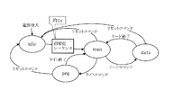
図9は、SDカード7の遷移状態を概略的に示す図である。SDカード7は、電源投入時は「idle」状態にあり、上述したCPU5による初期化(SDカード7による初期設定処理)によりCPU5によるアクセスが可能な「tran」状態に移行する。この場合、「idle」状態から「tran」状態となるまでの初期化シーケンスを実行するまで最大1秒要する。CPU5からリードコマンドを受けたときは「data」状態に移行し、リードが終了したときは「tran」状態に復帰する。CPU5からライトコマンドを受けたときは「prg」状態に移行し、ライトが終了したときは「tran」状態に復帰する。「tran」状態、「data」状態、「prg」状態の何れの状態においてCPU5からリセットコマンドを受けたときは「idle」状態に移行する。
FIG. 9 is a diagram schematically showing the transition state of the
続けてCPU5は、起動処理を実行する。
図4は、CPU5の起動処理を示すフローチャートである。CPU5は、リセットシーケンサ3のBUフラグ3bを読取り、BUフラグ3bがオンしているかを判定する。リセットシーケンサ3が起動した状態ではBUフラグ3bはオフしているので、待機処理を実行する。この待機処理とは、SDカード7が初期設定処理を実行するのに十分な時間待機するもので、例えば2秒が設定されている。待機処理終了後、BUフラグ3bをオンしてから、ブート処理を実行する。
Subsequently, the
FIG. 4 is a flowchart showing the startup process of the
図5はCPU5のブート処理の手順を示している。CPU5のROM5aにはブートローダーとSDドライバが予め記憶されており、まず、ブートローダーを読取ってから、SDカード7にアクセス可能となるようにSDドライバを起動したり、SDカード7との通信を行うためのI/Fを設定したりした後、SDカード7にIPLを読出す読出しコマンドを送信する。この場合、上述したようにSDカード7の初期設定処理が終了していることから、IPLを読取ることができ、そのIPLを実行することによりOSを読取ることができる。
FIG. 5 shows a procedure for boot processing of the
図2に戻って、CPU5をリセットしたリセットシーケンサ3は、CPU5の起動が終了するのを待機し(S6)、タイムアウトした場合は(S6:タイムアウト)、異常であると判定してCPU5をリセットすることによりCPU5を再起動する(S7)。一方、CPU5の起動が終了した場合は(S6:終了)、動作状態に移行し、CPU5が正常に動作しているかを監視しながら(S8)、アクセサリオン信号の受信状態が継続しているかを判定する(S9)。CPU5が正常動作しない場合は(S8:NG)、CPU5を繰り返してリセットする(S7)。
Returning to FIG. 2, the
図3は、リセットシーケンサ3によるCPU5のリセット動作を示している。CPU5は、起動後はタイマによる一定周期でウオッチドッグ用のクリア信号をリセットシーケンサ3に出力する。リセットシーケンサ3は、カウンタによるカウント動作を実行しており、規定時間内にCPU5からクリア信号を受信した場合はカウンタをクリアし、規定時間内にCPU5からクリア信号を受信しない場合はカウント値がFull(FFFF……)になると、異常であるとしてCPU5をリセットする。リセットの動作方式についてはこれに限らない。
FIG. 3 shows the reset operation of the
さて、リセットシーケンサ3は、アクセサリがオフされた場合は(S9:OFF)、終了処理状態に移行する。終了処理状態に移行すると、処理終了タイマを起動し、CPU5に割り込み(バックアップ指令に相当)を掛けてデータをバックアップする(S10)。
図6及び図7は、データバックアップの手順を示すフローチャートであり、2つの手順がある。図6に示す第1の手順では、CPU5に割り込みを掛けると、CPU5は、キャッシュメモリとして機能するRAM5bに記憶されているデータをDRAM6へ書き込み、SDカード7へのバックデータがあるかを判定し、バックアップデータがある場合は、DRAM6の該当するバックアップデータをSDカード7へ転送する。DRAM6にバックアップを要するデータがある(SDカード7にバックアップするのではなくDRAM6内にてバックアップしておくべきデータがある)場合は、DRAM6をセルフリフレッシュする。このセルフリフレッシュとは、DRAM6に内蔵されたリフレッシュ回路で自動的にリフレッシュを行えるようにしたもので、一度リフレッシュの命令を与えれば、DRAM6に電力を供給するだけでデータ保持が可能になるため、電力消費を抑えることができる。
When the accessory is turned off (S9: OFF), the
6 and 7 are flowcharts showing a data backup procedure, and there are two procedures. In the first procedure shown in FIG. 6, when the
一方、図7に示す第2の手順では、CPU5に割り込みを掛けると、CPU5は、RAM5bのデータをDRAM6に書込み、DRAM6にバックアップを要するデータがある場合は、DRAM6をセルフリフレッシュ状態とする。次に、SDカード7へのバックアップデータがある場合は、SDカード7へバックアップデータを書き込む。
以上のような手順により、CPU5のRAM5bに記憶されていたデータがバックアップされると共に、SDカード7にバックアップを要するデータが記憶される。
On the other hand, in the second procedure shown in FIG. 7, when the
Through the above procedure, the data stored in the
図2に戻って、リセットシーケンサ3は、終了処理状態で上述したようにデータのバックアップを試みた後、バックアップが正常に終了したかを判定し(S11)、タイマの時間内にバックアップが正常に終了したときは(S11:OK)、BU Endフラグを1とし(S12)、タイマをクリアしてから、電源4を停止することによりCPU5を停止する(S14)。一方、タイマがタイムオーバとなった場合は(S11:NG)、異常が生じたとして、電源4を停止すると共に電源スイッチ2をオフ・オンすることによりSDカード7をリセットする(S13)。これにより、SDカード7のコントローラ7aが次回のアクセサリオンを待つことなく初期設定処理を行い、異常状態を解消して次の起動(アクセサリオン)時に備えることができる。つまり、次回起動時にはすでに初期設定処理は終了しているため、ブート処理が直ちに実行され、その分迅速に外部の指令にこたえることが可能になる。
なお、このようなバックアップが正常に終了しない原因にはSDカード7の異常状態によるものと、CPU5の異常状態によるものとが想定される。SDカード7のリセットは前者を解消するものである。しかし、CPU5の異常状態によりバックアップが正常に終了しない状況に対してはSDカード7のリセットによる対応だけでは不十分である。
Returning to FIG. 2, after the
It should be noted that the reason why such a backup does not end normally is due to an abnormal state of the
そこで、本実施形態では、リセットシーケンサ3が電源4への給電指令を停止(S14における1.1/1.8/3.3V遮断)して終了処理状態からスタンバイ状態に移行すると、BU Endフラグに基づいてバックアップが完了したかをチェックするのである(S2)。BU Endフラグが1の場合は(S2:BU End=1)、バックアップが正常に完了したとして、起動要因が発生するまで待機する(S3)。当然この場合には、SDカード7はリセットされていないので、SDカード7は「tran」状態にあり、次のアクセサリオン時にはCPU5からの速やかなアクセスが可能となっている。一方、バックアップが正常に終了しなかったときは、BU Endフラグは0であることから(S2:BU End=0)アクセサリオンを待つことなく(ステップS3をスキップし)、ステップS4に移行して電源4を動作させて1.1/1.8/3.3VをCPU5へ投入してから(S4)、CPU5をリセットする(S5)。CPU5をリセットすることにより、CPU5側に発生している異常状態を解消することができる。なお、このステップS5におけるCPU5のリセット起動(再起動)にともない、自動的にSDカード7に対する初期化(SDカード7の初期設定処理)が行われる。
Therefore, in the present embodiment, when the
以下、CPU5の起動が終了(S6)し、CPU5が正常に動作していることを確認(S8:OK)すると、いまはアクセサリオフ状態で動作している(S9:OFF)ので、自動的にS10に移行しデータのバックアップを行う。そしてデータのバックアップが正常に終了した(S11:OK)ときは、BU Endフラグが1となり(S12)、SDカード7の「tran」状態が継続する。
このような動作によれば、アクセサリオフ時にデータバックアップが正常終了しなかった場合、次回アクセサリオンを待つことなく、SDカード7をリセットするので、次のアクセサリオンオンのタイミングまでには初期設定処理が終了し、SDカード7を「tran」状態とすることができる。よってアクセサリオン時にCPU5によるSDカード7に対するアクセスが直ちに可能となり、ソフトの起動が遅れてしまうことを防止できる。
また、SDカード7のリセットに加え、次のアクセサリオンを待つことなく、CPU5もリセット起動(再起動)し、データのバックアップをそれが正常終了するまで繰り返すので、データをSDカード7に正常かつ確実バックアップすることができる。
Hereinafter, when the activation of the
According to such an operation, if the data backup does not end normally when the accessory is turned off, the
In addition to resetting the
なお、上述でデータのバックアップが正常に終了しない場合(S11:NG→S13→S14)では、DRAM6にバックアップを試みたバックアップデータ(DRAM6へのバックアップを要するデータ)が異常となっている(データ自体が破損していたり、不完全となっていたりする)可能性があるため、DRAM6もリセットする必要がある。そこで、本実施形態ではリセットシーケンサ3が電源4への給電指令を停止(S14における1.1/1.8/3.3V遮断)するのに加え、このタイミングでオン状態の電源スイッチ11をオフしてオンすることにより、DRAM6への給電を停止し、再起動(リセット)する。これにより、DRAM(バックアップ用記憶手段)内に存在するバックアップデータの異常状態を確実に解消して初期状態とすることができ、DRAM6へ正常なバックアップを行うための準備を整えることができる。
If the data backup does not end normally (S11: NG → S13 → S14) as described above, the backup data (data that needs to be backed up to the DRAM 6) attempted to be backed up to the
また、SDカード7とCPU5との間のラインであるデータライン、アドレスライン、コマンドラインは、プルアップする必要があるものの、プルアップ抵抗9をBU電源8に接続した場合、CPU5への停止状態であってもBU電源8からの電圧がCPU5に回り込んでCPU5が不安定となる虞がある。
しかしながら、本実施形態では、プルアップ抵抗9をCPU5の電源ライン(3.3V)と接続するようにしたので、CPU5への給電が停止した状態ではプルアップ抵抗9の電圧は0Vとなり、CPU5に電圧が回り込んでしまうことを防止できる。
The data line, address line, and command line, which are lines between the
However, in this embodiment, since the pull-up
さて、車両が使用者に手渡され、使用者がアクセサリオン操作する場合は、SDカード7の初期設定処理が終了した状態でのアクセサリオン操作となる。この場合、SDカード7にはBU電源8からの給電状態が継続しており、リセットシーケンサ3のBUフラグ3bはオンしているので、図4の起動処理に示すように、リセットシーケンサ3により起動されたCPU5は、起動するにしても待機処理を実行することなくブート処理を実行してSDカード7からIPLを読取る。これにより、CPU5は、SDカード7からIPLを読取り、そのIPLの実行によりOSを読取るので、車内LANを通じた要求に確実に応えることができる。
そして、リセットシーケンサ3は、上述したように起動時にタイマがタイムアップした場合は、CPU5をリセットし、CPU5の動作状態では、CPU5が正常に動作しているかを監視し、使用者によりアクセサリオフ操作された場合は、データのバックアップを実行し、正常に終了しない場合は、SDカード7をリセットし、CPU5を強制終了すると同時にDRAMへの給電を停止(DRAM6をリセット)する。
Now, when the vehicle is handed over to the user and the user performs an accessory-on operation, the accessory-on operation is performed after the initial setting process of the
Then, as described above, the
このような実施形態によれば、次のような効果を奏することができる。
リセットシーケンサ3は、データのバックアップが正常に終了しなかったときは、アクセサリオンを待機することなくCPU5を起動してSDカード7を「idle」状態から「tran」状態に移行させるようにしたので、次のアクセサリオン時にCPU5によるSDカード7に対するアクセスが直ちに可能となり、ソフトの起動が遅くなってしまうことを防止できる。
CPU5は、BU電源8に接続されたリセットシーケンサ3が保持するバックアップフラグのオンオフにより待機処理を実行するか否かを判定するので、CPU5への給電が停止するにしても、起動したCPU5は、バックアップフラグのオンオフにより初期設定処理が行われているか否かを確実に判定することができる。
According to such an embodiment, the following effects can be produced.
Since the
Since the
リセットシーケンサ3は、アクセサリオン信号が停止した場合はCPU5に割り込みを掛け、CPU5がデータをバックアップするようにしたので、CPU5のRAM5bに記憶されているバックアップが必要な地図データをSDカード7に記憶することができる。また、地図データをSDカード7に記憶することができない場合は、異常が生じたとして電源スイッチ2、11及び電源4を停止するので、異常状態を解除して初期状態とすることができる。
CPU5への給電が停止した状態では、SDカード7とCPU5とを接続する各ラインはプルアップ抵抗9を通じて0Vとなるので、プルアップ抵抗9をバックアップ電源8に接続する構成に比較して、バックアップ電源8からSDカード7とCPU5とを接続する各ラインの保護カードなどを介してCPU5に電圧が回り込んで不安定となってしまうことを防止できる。
When the accessory on signal stops, the
In the state where the power supply to the
(第2実施形態)
次に、本発明の第2実施形態について図10を参照して説明する。この第2実施形態は、バックアップが正常に終了しなかったときは、CPU5の起動後にデータをバックすることを特徴とする。
図10はリセットシーケンサ3の動作を示しており、図2に示す動作のステップと同一ステップには同一のステップ番号を付し、異なるステップに新たなステップ番号を付して説明する。
リセットシーケンサ3は、アクセサリオンに応じてCPU5の起動が終了したときは(S6:終了)、BU Endフラグ=0かを判定し(S21)、BU Endフラグ=0の場合は(S21:BU End=0)、データのバックアップは正常に終了しなかったと判定してデータをバックアップし(S22)、バックアップが正常終了したときは(S23:OK)、BU Endフラグ=1としてステップS8に移行する。
(Second Embodiment)
Next, a second embodiment of the present invention will be described with reference to FIG. The second embodiment is characterized in that data is backed up after activation of the
FIG. 10 shows the operation of the
The
さて、データのバックアップが正常に終了しなかったとき(S23:NG)は、アクセサリオフを待つことなく(S9などをスキップして)、SDカード7をリセットし、初期設定処理を行ってSDカード7側の異常状態を解消する。つまり、この時点でSDカード7は「tran」状態となる。そしてCPU5を再起動(S14→S2:BU End=0→S4→S5→S6:終了)し、前記「tran」状態となったところでSDカード7に対してデータのバックアップが行われる(S22)である。
この後最終的にアクセサリオフ後のデータバックアップが正常に終了した場合には(S23:OK→S24→S8:OK→S9:OFF→S10→S11:OK→S12)SDカード7の「tran」状態がアクセサリオフでも継続するので、次のアクセサリオン時にはSDカード7が「tran」状態となっており、CPU5によるSDカード7に対するアクセスが直ちに可能となる。
When the data backup is not completed normally (S23: NG), the
After this, if the data backup after the accessory is turned off is completed normally (S23: OK → S24 → S8: OK → S9: OFF → S10 → S11: OK → S12), the “trans” state of the
このような実施形態によれば、データのバックアップが正常に終了しなかった場合であっても、次のアクセサリオンまでにSDカード7を「idle」状態から「tran」状態に移行するようにしたので、第1実施形態と同様に、アクセサリオン時にCPU5によるSDカード7に対するアクセスが直ちに可能となり、ソフトの起動が遅くなってしまうことを防止できる。
また、CPU5の起動直後にデータのバックアップを行うようにしたので、バックアップに失敗したデータを確実にバックアップすることができる。なお、この実施形態2ではデータのバックアップが2段階に行われる(S22、S10)ためよりバックアップを確実にすることができるようになる。
According to such an embodiment, the
In addition, since the data is backed up immediately after the
(その他の実施形態)
本発明は、上記実施形態に限定されることなく、次のように変形または拡張できる。
CPU5は、電源4の起動時にSDカード7が応答しない場合は初期設定処理未終了であると判断して初期設定処理を実行し、起動時にSDカード7が応答した場合は初期設定処理終了であると判断して初期設定処理を実行することなくブート処理を実行するようにしても良い。このような構成によれば、リセットシーケンサ3にバックアップ用フラグを設ける必要がないことから、リセットシーケンサ3の構成を簡単化することができる。
本発明をカーナビ以外の車両用装置に適用するようにしてもよい。
(Other embodiments)
The present invention is not limited to the above embodiment, and can be modified or expanded as follows.
If the
You may make it apply this invention to apparatuses for vehicles other than a car navigation system.
図面中、1は車両用ナビゲーション装置(車両用装置)、2は電源スイッチ、3はリセットシーケンサ(電源制御手段)、4は電源、5はCPU(制御手段に相当)、6はDRAM(バックアップ用記憶手段)、7はSDカード(記憶手段)、7aはコントローラ、7cはNAND型フラッシュメモリ、8はバックアップ電源である。 In the drawings, 1 is a vehicle navigation device (vehicle device), 2 is a power switch, 3 is a reset sequencer (power control means), 4 is a power supply, 5 is a CPU (corresponding to control means), and 6 is a DRAM (for backup) Storage means), 7 is an SD card (storage means), 7a is a controller, 7c is a NAND flash memory, and 8 is a backup power supply.
Claims (7)
車両に搭載されたバッテリの電圧を第1電圧に変圧するバックアップ電源と、
前記バックアップ電源と接続され、オン状態で前記バックアップ電源から前記第1電圧を前記記憶手段に給電する電源スイッチと、
前記バックアップ電源と接続され、給電指令を受けたときは前記第1電圧から第2電圧を生成する電源と、
前記電源と接続され、前記電源から前記第2電圧が給電されると起動し、起動すると前記記憶手段のコントローラによる初期設定処理が終了しているか否かを判定し、初期設定処理未終了であると判定した場合は、初期設定処理が終了するのを待機する待機処理を実行してから前記記憶手段からブートプラグムを読込むブート処理を実行し、初期設定処理終了であると判定した場合は、前記待機処理を実行することなく前記ブート処理を実行すると共に、データのバックアップ指令を受けたときは、バックアップを必要とするデータを前記記憶手段に記憶する制御手段と、
前記バックアップ電源と接続され、前記バックアップ電源から前記第2電圧が給電されると起動し、起動すると前記電源スイッチをオンしてから車両の起動要因が発生するのを待機する起動要因待機状態となり、前記起動要因待機状態となってから、起動要因が発生した場合は前記電源に給電指令を与え、その後前記車両の起動要因が終了した場合は前記制御手段に前記バックアップ指令を与え、前記制御手段がデータのバックアップを正常終了したときは前記電源に対する給電指令を停止してから前記起動要因待機状態となり、正常終了しなかったときは前記オンした電源スイッチをオフしてまたオンするリセットを行うと共に前記電源に対する給電指令を停止してから再び給電指令を与える電源制御手段と、
を備えたことを特徴とする車両用装置。 Search NAND flash memory storing at least bootplum and the program read by executing the bootpragm, and all defective blocks of the NAND flash memory when power is turned on, and exclude the detected defective block Storage means having a controller for executing an initial setting process for managing the correspondence between the logical block and the physical block;
A backup power source for transforming the voltage of the battery mounted on the vehicle to the first voltage;
A power switch connected to the backup power supply and supplying the first voltage from the backup power supply to the storage means in an ON state;
A power source that is connected to the backup power source and generates a second voltage from the first voltage when receiving a power supply command;
When the second voltage is supplied from the power supply, the power supply is activated, and when activated, it is determined whether or not the initial setting process by the controller of the storage means has been completed, and the initial setting process has not been completed. If it is determined that the initial setting process is completed, a standby process that waits for completion of the initial setting process is executed, and then a boot process that reads the bootplum from the storage unit is executed. , Executing the boot process without executing the standby process, and when receiving a data backup command, control means for storing data that requires backup in the storage means;
It is connected to the backup power source and activated when the second voltage is supplied from the backup power source, and when activated, the power switch is turned on to wait for an activation factor of the vehicle to be generated, and an activation factor standby state is established. When the activation factor is generated after entering the activation factor standby state, a power supply command is given to the power source, and when the vehicle activation factor is finished, the backup command is given to the control means. When the backup of data is normally completed, the power supply command to the power supply is stopped and then the activation factor standby state is entered.When the backup is not normally completed, the power switch that is turned on is turned off and the reset is performed to turn it on again. Power supply control means for supplying a power supply command again after stopping the power supply command to the power supply;
A vehicle apparatus comprising:
前記制御手段は、当該制御手段の起動時に前記初期設定処理判定値が前記第1の値の場合は前記記憶手段の初期設定処理未終了であると判断すると共に初期設定処理終了後に前記初期設定処理判定値を第2の値とし、一方当該制御手段の起動時に前記初期設定処理判定値が第2の値の場合は前記記憶手段のコントローラによる初期設定処理終了であると判断することを特徴とする請求項1または2記載の車両用装置。 The power control unit stores a determination value indicating whether or not the initial setting process has been completed, and an initial setting process determination value determined to be a first value when the power control unit is activated. Provided in
The control means determines that the initial setting process of the storage means has not been completed if the initial setting process determination value is the first value when the control means is activated, and the initial setting process after the initial setting process is completed. The determination value is a second value. On the other hand, if the initial setting process determination value is the second value when the control unit is activated, it is determined that the initial setting process by the controller of the storage unit is completed. The apparatus for vehicles of Claim 1 or 2.
前記制御手段は、バックアップが必要なデータを前記バックアップ用記憶手段に記憶し、バックアップを正常に終了できなかった場合は異常が生じたとして前記バックアップ用記憶手段への給電を停止することを特徴とする請求項1ないし4の何れかに記載の車両用装置。 Powered by the backup power source, comprising backup storage means for storing backup data,
The control means stores data that needs to be backed up in the backup storage means, and stops power supply to the backup storage means if an abnormality has occurred if the backup cannot be completed normally. The vehicle apparatus according to any one of claims 1 to 4.
Priority Applications (5)
| Application Number | Priority Date | Filing Date | Title |
|---|---|---|---|
| JP2011222783A JP5382084B2 (en) | 2011-10-07 | 2011-10-07 | Vehicle equipment |
| US13/628,858 US8832359B2 (en) | 2011-10-07 | 2012-09-27 | In-vehicle apparatus |
| CN201210410049.5A CN103034509B (en) | 2011-10-07 | 2012-09-28 | Mobile unit |
| KR1020120109187A KR101333641B1 (en) | 2011-10-07 | 2012-09-28 | In-vehicle apparatus |
| TW101136860A TWI492867B (en) | 2011-10-07 | 2012-10-05 | In-vehicle apparatus |
Applications Claiming Priority (1)
| Application Number | Priority Date | Filing Date | Title |
|---|---|---|---|
| JP2011222783A JP5382084B2 (en) | 2011-10-07 | 2011-10-07 | Vehicle equipment |
Publications (2)
| Publication Number | Publication Date |
|---|---|
| JP2013084089A JP2013084089A (en) | 2013-05-09 |
| JP5382084B2 true JP5382084B2 (en) | 2014-01-08 |
Family
ID=48021435
Family Applications (1)
| Application Number | Title | Priority Date | Filing Date |
|---|---|---|---|
| JP2011222783A Expired - Fee Related JP5382084B2 (en) | 2011-10-07 | 2011-10-07 | Vehicle equipment |
Country Status (5)
| Country | Link |
|---|---|
| US (1) | US8832359B2 (en) |
| JP (1) | JP5382084B2 (en) |
| KR (1) | KR101333641B1 (en) |
| CN (1) | CN103034509B (en) |
| TW (1) | TWI492867B (en) |
Families Citing this family (15)
| Publication number | Priority date | Publication date | Assignee | Title |
|---|---|---|---|---|
| CN104521146B (en) * | 2012-09-06 | 2017-09-22 | 松下知识产权经营株式会社 | Semiconductor integrated circuit |
| CN103744746B (en) * | 2013-12-30 | 2016-08-03 | 北京工业大学 | A kind of intelligent card records backup based on index and restoration methods |
| CN103942130B (en) * | 2014-04-28 | 2015-11-18 | 山东华芯半导体有限公司 | A kind of sequential control method of SD snap gauge type |
| DE102014016842A1 (en) * | 2014-11-13 | 2016-05-19 | Technisat Digital Gmbh | Starting data services of a navigation device of a vehicle |
| JP6430896B2 (en) | 2015-06-05 | 2018-11-28 | アルパイン株式会社 | Standby processing control apparatus and standby processing control method for electronic device |
| DE102015118659A1 (en) * | 2015-10-30 | 2017-05-04 | Minebea Co., Ltd. | Method and system for controlling the operation of a control device |
| CN105956194A (en) * | 2016-06-18 | 2016-09-21 | 张阳康 | Processing method of electric energy network data |
| JP6643210B2 (en) * | 2016-09-09 | 2020-02-12 | 本田技研工業株式会社 | Vehicle data reading device and vehicle data reading method |
| KR102258171B1 (en) | 2017-12-15 | 2021-05-28 | 주식회사 엘지에너지솔루션 | Apparatus and method for diagnosing a watchdog timer |
| CN112078524B (en) * | 2019-06-12 | 2022-03-29 | 北京车和家信息技术有限公司 | Application state control method and device, vehicle and computer readable storage medium |
| WO2020261519A1 (en) * | 2019-06-27 | 2020-12-30 | 三菱電機株式会社 | Electronic control unit and program |
| CN114175004B (en) * | 2019-07-12 | 2024-04-23 | 松下知识产权经营株式会社 | Vehicle-mounted storage system |
| DE102020200203B4 (en) * | 2020-01-09 | 2022-01-20 | Vitesco Technologies GmbH | Device for operating an electronic system, in particular a vehicle |
| JP7097630B2 (en) * | 2020-11-04 | 2022-07-08 | 株式会社ユピテル | unit |
| CN112437134B (en) * | 2020-11-11 | 2022-06-24 | 浙江吉利控股集团有限公司 | Control method and control system for vehicle-mounted double hosts |
Family Cites Families (10)
| Publication number | Priority date | Publication date | Assignee | Title |
|---|---|---|---|---|
| JP3324148B2 (en) * | 1992-08-13 | 2002-09-17 | 株式会社デンソー | Inspection device for backup memory |
| JP3776493B2 (en) | 1995-12-27 | 2006-05-17 | オリンパス株式会社 | Image recording device |
| JP3500919B2 (en) | 1997-07-30 | 2004-02-23 | 株式会社デンソー | Vehicle navigation system |
| JP4079506B2 (en) | 1997-08-08 | 2008-04-23 | 株式会社東芝 | Method for controlling nonvolatile semiconductor memory system |
| US6862651B2 (en) * | 2000-12-20 | 2005-03-01 | Microsoft Corporation | Automotive computing devices with emergency power shut down capabilities |
| JP2002342176A (en) * | 2001-05-21 | 2002-11-29 | Hitachi Ltd | Method for restoring data in semiconductor memory |
| KR100610354B1 (en) * | 2002-03-19 | 2006-08-09 | 삼성전자주식회사 | Controlling apparatus and method for information process system of mobile terminal apparatus using flash memory |
| JP2006178901A (en) | 2004-12-24 | 2006-07-06 | Mitsubishi Electric Corp | Power circuit for on-vehicle information device, and on-vehicle information device using the circuit |
| JP5321438B2 (en) | 2009-12-14 | 2013-10-23 | 株式会社リコー | Electronic device, activation control method, activation control program, and recording medium |
| JP5077385B2 (en) | 2010-04-15 | 2012-11-21 | 株式会社デンソー | Vehicle navigation device |
-
2011
- 2011-10-07 JP JP2011222783A patent/JP5382084B2/en not_active Expired - Fee Related
-
2012
- 2012-09-27 US US13/628,858 patent/US8832359B2/en not_active Expired - Fee Related
- 2012-09-28 KR KR1020120109187A patent/KR101333641B1/en active IP Right Grant
- 2012-09-28 CN CN201210410049.5A patent/CN103034509B/en not_active Expired - Fee Related
- 2012-10-05 TW TW101136860A patent/TWI492867B/en not_active IP Right Cessation
Also Published As
| Publication number | Publication date |
|---|---|
| KR101333641B1 (en) | 2013-11-27 |
| US8832359B2 (en) | 2014-09-09 |
| KR20130038149A (en) | 2013-04-17 |
| CN103034509B (en) | 2015-12-16 |
| JP2013084089A (en) | 2013-05-09 |
| US20130091323A1 (en) | 2013-04-11 |
| CN103034509A (en) | 2013-04-10 |
| TW201345760A (en) | 2013-11-16 |
| TWI492867B (en) | 2015-07-21 |
Similar Documents
| Publication | Publication Date | Title |
|---|---|---|
| JP5382084B2 (en) | Vehicle equipment | |
| US11960877B2 (en) | Updating system, electronic control unit, updating management device, and updating management method | |
| US20180341476A1 (en) | Software updating device, software updating system, and software updating method | |
| JP5229326B2 (en) | Power consumption control method, power consumption control program and information processing system in multi-core CPU | |
| JP6424797B2 (en) | In-vehicle device | |
| WO2012079400A1 (en) | Method and apparatus for upgrading embedded system bootrom | |
| JP5077385B2 (en) | Vehicle navigation device | |
| JP6723941B2 (en) | Control device and control program updating method | |
| JP2007334403A (en) | System and method for supporting trouble of computer system | |
| KR101115149B1 (en) | Apparatus for a fast booting and managing power in a car system with a plurality of peripherals | |
| JP7131481B2 (en) | vehicle equipment | |
| JP2020021506A (en) | Electronic controller and session establishing program | |
| WO2022028350A1 (en) | Electronic device and method for controlling update of data in electronic device | |
| JP6385322B2 (en) | Information processing device | |
| CN113650498B (en) | Power-on method and device of electric vehicle, electric vehicle and storage medium | |
| JP6102692B2 (en) | Electronic control unit | |
| JP7291541B2 (en) | Control device and monitoring method | |
| JP7378445B2 (en) | Electronic control unit, information processing method, and program | |
| US20240211239A1 (en) | Electronic control unit | |
| CN118151986A (en) | Software consistency checking method, device, electronic device and storage medium | |
| CN116476763A (en) | Hierarchical power management system and method for vehicles | |
| JP2003280907A (en) | Information processing system, configuration management method of the same, program for configuration management | |
| JPH05250193A (en) | Start control system |
Legal Events
| Date | Code | Title | Description |
|---|---|---|---|
| A621 | Written request for application examination |
Free format text: JAPANESE INTERMEDIATE CODE: A621 Effective date: 20130306 |
|
| A977 | Report on retrieval |
Free format text: JAPANESE INTERMEDIATE CODE: A971007 Effective date: 20130828 |
|
| TRDD | Decision of grant or rejection written | ||
| A01 | Written decision to grant a patent or to grant a registration (utility model) |
Free format text: JAPANESE INTERMEDIATE CODE: A01 Effective date: 20130903 |
|
| A61 | First payment of annual fees (during grant procedure) |
Free format text: JAPANESE INTERMEDIATE CODE: A61 Effective date: 20130916 |
|
| R151 | Written notification of patent or utility model registration |
Ref document number: 5382084 Country of ref document: JP Free format text: JAPANESE INTERMEDIATE CODE: R151 |
|
| A977 | Report on retrieval |
Free format text: JAPANESE INTERMEDIATE CODE: A971007 Effective date: 20131017 |
|
| R250 | Receipt of annual fees |
Free format text: JAPANESE INTERMEDIATE CODE: R250 |
|
| R250 | Receipt of annual fees |
Free format text: JAPANESE INTERMEDIATE CODE: R250 |
|
| R250 | Receipt of annual fees |
Free format text: JAPANESE INTERMEDIATE CODE: R250 |
|
| R250 | Receipt of annual fees |
Free format text: JAPANESE INTERMEDIATE CODE: R250 |
|
| LAPS | Cancellation because of no payment of annual fees |