JP5380997B2 - Diversity antenna device and electronic device using the same - Google Patents
Diversity antenna device and electronic device using the same Download PDFInfo
- Publication number
- JP5380997B2 JP5380997B2 JP2008265984A JP2008265984A JP5380997B2 JP 5380997 B2 JP5380997 B2 JP 5380997B2 JP 2008265984 A JP2008265984 A JP 2008265984A JP 2008265984 A JP2008265984 A JP 2008265984A JP 5380997 B2 JP5380997 B2 JP 5380997B2
- Authority
- JP
- Japan
- Prior art keywords
- antenna element
- phase shifter
- variable
- variable phase
- antenna
- Prior art date
- Legal status (The legal status is an assumption and is not a legal conclusion. Google has not performed a legal analysis and makes no representation as to the accuracy of the status listed.)
- Expired - Fee Related
Links
Images


Classifications
-
- H—ELECTRICITY
- H01—ELECTRIC ELEMENTS
- H01Q—ANTENNAS, i.e. RADIO AERIALS
- H01Q21/00—Antenna arrays or systems
- H01Q21/24—Combinations of antenna units polarised in different directions for transmitting or receiving circularly and elliptically polarised waves or waves linearly polarised in any direction
-
- H—ELECTRICITY
- H04—ELECTRIC COMMUNICATION TECHNIQUE
- H04B—TRANSMISSION
- H04B7/00—Radio transmission systems, i.e. using radiation field
- H04B7/02—Diversity systems; Multi-antenna system, i.e. transmission or reception using multiple antennas
- H04B7/04—Diversity systems; Multi-antenna system, i.e. transmission or reception using multiple antennas using two or more spaced independent antennas
- H04B7/08—Diversity systems; Multi-antenna system, i.e. transmission or reception using multiple antennas using two or more spaced independent antennas at the receiving station
- H04B7/0837—Diversity systems; Multi-antenna system, i.e. transmission or reception using multiple antennas using two or more spaced independent antennas at the receiving station using pre-detection combining
- H04B7/0842—Weighted combining
- H04B7/0848—Joint weighting
- H04B7/0857—Joint weighting using maximum ratio combining techniques, e.g. signal-to- interference ratio [SIR], received signal strenght indication [RSS]
-
- H—ELECTRICITY
- H04—ELECTRIC COMMUNICATION TECHNIQUE
- H04B—TRANSMISSION
- H04B7/00—Radio transmission systems, i.e. using radiation field
- H04B7/02—Diversity systems; Multi-antenna system, i.e. transmission or reception using multiple antennas
- H04B7/10—Polarisation diversity; Directional diversity
Landscapes
- Engineering & Computer Science (AREA)
- Computer Networks & Wireless Communication (AREA)
- Signal Processing (AREA)
- Radio Transmission System (AREA)
- Variable-Direction Aerials And Aerial Arrays (AREA)
Description
本発明は、例えば、無線通信機器に使用できる最大比合成方式または等利得合成方式のダイバーシティアンテナ装置に関するものである。 The present invention relates to a diversity antenna apparatus of a maximum ratio combining method or an equal gain combining method that can be used for, for example, a wireless communication device.
例えば、無線通信機器に使用可能な従来の等利得合成方式のダイバーシティアンテナ装置について、図28、29を用いて説明する。 For example, a conventional equal gain combining type diversity antenna apparatus usable for a wireless communication device will be described with reference to FIGS.
図28において、従来の等利得合成方式のダイバーシティアンテナ装置のアンテナエレメント部分は、第1ダイポールアンテナ100と第2ダイポールアンテナ101とが直交配置されたクロスダイポールアンテナ102が用いられている。クロスダイポールアンテナ102の特長は、2つのダイポールアンテナの間の相関が低い点である。これは、2つのダイポールアンテナの偏波が直交していることに起因している。
In FIG. 28, a
クロスダイポールアンテナ102のように2つのアンテナエレメントの相関係数の低いアンテナエレメントをダイバーシティアンテナ装置に用いれば、ダイバーシティアンテナ装置の受信特性を良好なものとすることができる。
If an antenna element having a low correlation coefficient between two antenna elements, such as the
図29を用いて、従来のダイバーシティアンテナ装置の回路部111を示す。図28の第1ダイポールアンテナ100の給電部103は、図29の第1バラン105へ接続され、平衡/不平衡変換がなされる。同様に、図28の第2ダイポールアンテナ101の給電部104は、図29の第2バラン106へ接続され、平衡/不平衡変換がなされる。
A circuit unit 111 of a conventional diversity antenna device is shown using FIG. The
第1バラン105の出力信号は第1可変移相器107へ入力されると共に、第2バラン106の出力信号は第2可変移相器108へ入力され、それぞれの入力信号の位相が変化した後、合成器109において、それぞれの信号は足し合わされる。
The output signal of the
合成器109の出力信号は、信号処理部110に入力され、この信号処理部110において、入力信号は復調され、C/N(Carrier/Noise)比やBER(Bit Error Rate)等の受信信号の品質を表す信号品質値が導出される。そして、この導出された信号品質値を基に、信号処理部110は、第1可変移相器107および第2可変移相器108の移相量を、信号品質値が最良となるように制御する。
The output signal of the synthesizer 109 is input to the
尚、本出願の発明に関連する先行技術文献情報としては、例えば、特許文献1が知られている。
上記従来のダイバーシティアンテナ装置において、アンテナ部に用いたクロスダイポールアンテナ102は、アンテナ間の相関係数は低いという長所を有しているが、同時に、アンテナサイズが大きく、形状の保持等を考えると構造が複雑化するという課題を有していた。また、アンテナサイズを小さくし、アンテナ構造を単純化するために、クロスダイポールアンテナ102の代わりに、図29の従来のダイバーシティアンテナ装置の回路部111が実装されたグランド(図示せず)上に2本のモノポールアンテナ配置し、この2本のモノポールアンテナを用いて等利得合成方式のダイバーシティ受信を行う事も考えられる。しかし、この場合には、2本のモノポールアンテナの偏波を直交させることが不可能であるため、2本のモノポールアンテナ間の相関係数を低くする事が困難であり、ダイバーシティアンテナ装置の受信特性が劣化するという課題を有していた。
In the above-described conventional diversity antenna device, the
そこで本発明は、2つのアンテナエレメントのアンテナサイズが小さく、構造が単純であるにも関わらず、2つのアンテナエレメント間の相関係数が低く、受信特性の優れたダイバーシティアンテナ装置を提供することを目的とする。 Accordingly, the present invention provides a diversity antenna device having excellent reception characteristics with a low correlation coefficient between the two antenna elements even though the antenna sizes of the two antenna elements are small and the structure is simple. Objective.
この目的を達成するために、本発明のダイバーシティアンテナ装置は、第1アンテナエレメントと、第2アンテナエレメントと、第1アンテナエレメントに電気的に接続された第1可変移相器と、第2アンテナエレメントに電気的に接続された第2可変移相器と、第1可変移相器の出力信号と第2可変移相器の出力信号とを合成する合成器と、合成器の出力側に電気的に接続される信号処理部とを有し、信号処理部は、前記信号処理部に入力される信号の信号品質値を導出し、この信号品質値に基づいて第1可変移相器と第2可変移相器の移相量を制御すると共に、第1アンテナエレメントの入力インピーダンスと第2アンテナエレメントの入力インピーダンスとは概ね同一値であり、第1アンテナエレメントと第2アンテナエレメントのそれぞれの偏波が交差する点において、それぞれの偏波は所定の角度θを有しており、角度θ≠90度であり、且つ、角度θ≠0度であるダイバーシティアンテナ装置である。 In order to achieve this object, a diversity antenna apparatus of the present invention includes a first antenna element, a second antenna element, a first variable phase shifter electrically connected to the first antenna element, and a second antenna. A second variable phase shifter electrically connected to the element; a synthesizer that combines the output signal of the first variable phase shifter and the output signal of the second variable phase shifter; A signal processing unit connected to the signal processing unit, wherein the signal processing unit derives a signal quality value of the signal input to the signal processing unit, and based on the signal quality value, the first variable phase shifter and the first 2 The phase shift amount of the variable phase shifter is controlled, and the input impedance of the first antenna element and the input impedance of the second antenna element are substantially the same value. In that polarization, respectively intersect each polarization has a predetermined angle theta, the angle theta ≠ 90 degrees, and a diversity antenna apparatus is the angle theta ≠ 0 °.
本発明のダイバーシティアンテナ装置の第1アンテナエレメントの入力インピーダンスと第2アンテナエレメントの入力インピーダンスとは概ね同一値であるので、第1アンテナエレメントと第2アンテナエレメントの出力信号が偶(even)モードである場合と、第1アンテナエレメントと第2アンテナエレメントの出力信号が奇(odd)モードである場合とで、第1アンテナエレメントと第2アンテナエレメントとの合成の放射パターンの偏波が直交することとなる。この動作原理の詳細については、後述する。 Since the input impedance of the first antenna element and the input impedance of the second antenna element of the diversity antenna apparatus of the present invention are substantially the same value, the output signals of the first antenna element and the second antenna element are in even mode. In some cases, and in the case where the output signals of the first antenna element and the second antenna element are in the odd mode, the polarization of the combined radiation pattern of the first antenna element and the second antenna element is orthogonal. It becomes. Details of this operation principle will be described later.
これにより、例えば、2本のモノポールアンテナのような小型なアンテナエレメント(それぞれの放射パターンの偏波は直交していない)を用いても、給電のモード(偶モード及び奇モードの2つの給電方法)により、2つのモノポールアンテナの合成の放射パターンにおいては、直交する2つの偏波を得る事ができ、最大比合成方式および等利得合成方式のダイバーシティ方式において、良好な受信特性を得る事ができる。 Thus, for example, even if a small antenna element such as two monopole antennas (the polarizations of the respective radiation patterns are not orthogonal), two feeding modes (even mode and odd mode) are fed. Method), two orthogonal polarizations can be obtained in the combined radiation pattern of the two monopole antennas, and good reception characteristics can be obtained in the maximum ratio combining method and the equal gain combining diversity method. Can do.
(実施の形態1)
以下、本発明の実施の形態1について、図1を用いて説明する。図1は、本発明のダイバーシティアンテナ装置のブロック図である。
(Embodiment 1)
Hereinafter,
図1において、本発明のダイバーシティアンテナ装置1は、第1アンテナエレメント2と、第2アンテナエレメント3と、第1アンテナエレメント2に電気的に接続された第1可変移相器4と、第2アンテナエレメント3に電気的に接続された第2可変移相器5と、第1可変移相器4の出力信号と第2可変移相器5の出力信号とを合成する合成器6と、合成器6の出力側に電気的に接続される信号処理部7とを有している。
In FIG. 1, a
そして、信号処理部7は、信号処理部7に入力される信号の信号品質値を導出し、この信号品質値に基づいて第1可変移相器4と第2可変移相器5の移相量を制御する。
Then, the
また、第1アンテナエレメント2と第2アンテナエレメント3のそれぞれの偏波が交差する点において、それぞれの偏波は所定の角度θを有しており、角度θ≠0度で且つ、θ≠90度である。
Further, at the point where the respective polarized waves of the
ここで、特許請求の範囲における「第1アンテナエレメントと第2アンテナエレメントのそれぞれの偏波」とは、第1アンテナエレメント2の偏波と第2アンテナエレメント3の偏波とを指している。ここで「第1アンテナエレメント2の偏波」とは、「第1アンテナエレメント2のみに給電した場合(第2アンテナエレメント3には給電せず、第2アンテナエレメント3の直下に負荷抵抗が接続されていると仮定)の偏波を指している。また、「第2アンテナエレメント3の偏波」とは、第2アンテナエレメント3のみに給電した場合(第1アンテナエレメント2には給電せず、第1アンテナエレメント2の直下に負荷抵抗が接続されていると仮定)の偏波とを指している。
Here, the “polarization of each of the first antenna element and the second antenna element” in the claims refers to the polarization of the
また、第1アンテナエレメント2と第2アンテナエレメント3とが、グランド板(図示せず)と共にアンテナ動作するモノポールアンテナのようなアンテナである場合は、グランド板と共にアンテナ動作した結果の偏波を指している。
When the
尚、特許請求の範囲においては、偏波が直線偏波である場合の各直線偏波の配置要件を記載したが、第1アンテナエレメント2と第2アンテナエレメント3の内、少なくとも一方のアンテナエレメントの偏波が楕円偏波又は円偏波の場合は、偏波方向が時間的に変化する事となるため、定常的に角度θ=0度又はθ=90度で維持される事はない。このため、第1アンテナエレメント2と第2アンテナエレメント3の内、少なくとも一方のアンテナエレメントの偏波が楕円偏波又は円偏波の場合は、本発明のダイバーシティアンテナ装置が有する顕著な効果を発揮する事ができる。
In the claims, the arrangement requirement of each linearly polarized wave when the polarized wave is a linearly polarized wave is described, but at least one of the
更に、特許請求の範囲における「それぞれの直線偏波が交差する点」とは、それぞれの直線偏波が直接的に交わる点のみを指しているのではなく、直接的に交わっておらず立体的に交わる点をも含んでいる(つまり、それぞれの直線偏波が平行に配置されていなければ、必ず、それぞれの直線偏波は直接的又は立体的に交わっている事になる)。ここで、それぞれの直線偏波が立体的に交差している場合に、それぞれの直線偏波が交差する点とは、それぞれの直線偏波に対し平行な1つの面を想起し、その面の鉛直方向からそれぞれの直線偏波を見た時の、それぞれの直線偏波が交差する点を指している。同様に、特許請求の範囲における「所定の角度θ」とは、それぞれの直線偏波に対し平行な1つの面を想起し、その面の鉛直方向からそれぞれの直線偏波を見た時の、それぞれの直線偏波が成す角度を指している。 Furthermore, in the claims, “the point where each linearly polarized wave intersects” does not mean only the point where each linearly polarized wave directly intersects, but it does not intersect directly but is three-dimensional. (In other words, if the linearly polarized waves are not arranged in parallel, the linearly polarized waves always intersect directly or three-dimensionally). Here, when each linearly polarized wave intersects three-dimensionally, the point where each linearly polarized wave intersects recalls one plane parallel to each linearly polarized wave, When the respective linearly polarized waves are viewed from the vertical direction, they indicate points where the respective linearly polarized waves intersect. Similarly, “predetermined angle θ” in the claims refers to one plane parallel to each linearly polarized wave, and when each linearly polarized wave is viewed from the vertical direction of the plane, It refers to the angle formed by each linearly polarized wave.
角度θが0度の場合、近接して配置された第1アンテナエレメント2と第2アンテナエレメント3のそれぞれの直線偏波が同一方向に揃ってしまうため、第1アンテナエレメント2と第2アンテナエレメント2とで受信される信号がほぼ同一のものとなってしまう。その結果、ダイバーシティアンテナの効果が無くなり、物理的に2本のアンテナエレメントを用いながら、実質的に1本分のアンテナエレメントを用いた場合と同等性能しか得られないこととなる。よって、角度θ=0度の場合は、本発明のダイバーシティアンテナ装置が有する有利な効果が得られないため、特許請求の範囲からこの部分を除く事とした。
When the angle θ is 0 degree, the
以下、図1を用いて、本発明のダイバーシティアンテナ装置1の動作について説明する。
Hereinafter, the operation of the
第1アンテナエレメント2で受信された信号は、第1可変移相器4に入力される。そして、第1可変移相器4は、入力された信号の位相を所定の移相量だけ回転させた後、第1可変増幅器8へ出力する。第1可変増幅器8は、入力された信号の振幅を所定量だけ増幅させた後、合成器6へ出力する。
A signal received by the
第2アンテナエレメント3で受信された信号は、第2可変移相器5に入力される。そして、第2可変移相器5は、入力された信号の位相を所定の移相量だけ回転させた後、第2可変増幅器9へ出力する。第2可変増幅器9は、入力された信号の振幅を所定量だけ増幅させた後、合成器6へ出力する。
The signal received by the
合成器6は、第1可変増幅器8と第2可変増幅器9とから入力される信号を足し合わせた後、復調回路(図示せず)へ出力される。
The synthesizer 6 adds the signals input from the first
合成器6の出力信号の一部は信号処理部7に入力されると共に、信号処理部7は、入力された信号の信号品質値を導出する。ここで、信号品質値とは、信号の品質を表す指標を指しており、具体的には、BER(Bit Error Rate)やC/N(Carrier/Noise)、S/N(Signal/Noise)等の指標を指している。そして、信号処理部7は、導出された信号品質値が最も良化するように、第1可変移相器4と第2可変移相器5のそれぞれの移相量と、第1可変増幅器8と第2可変増幅器9のそれぞれの利得とを制御する。
A part of the output signal of the combiner 6 is input to the
本発明のダイバーシティアンテナ装置1の構成において、特徴的な構成は、第1アンテナエレメント2の入力インピーダンスと前記第2アンテナエレメントの入力インピーダンスとが概ね同一値である点である。
In the configuration of the
以下、なぜこの構成により良好な受信特性が得られるのかについて、図2を用いて説明する。 The reason why good reception characteristics can be obtained with this configuration will be described below with reference to FIG.
図2に示すダイバーシティアンテナ装置10は、近接して配置された第1アンテナエレメント2と第2アンテナエレメント3と、第1アンテナエレメント2と電気的に接続される第1給電部11と、第2アンテナエレメント3と電気的に接続される第2給電部12と、第1給電部11と第2給電部12とが電気的に接続されるグランド板13とを有している。尚、図2においては、簡略化のため第1給電部11と第2給電部12を用いて表現しているが、実際的には、第1給電部11と第2給電部12は、図1の第1可変移相器4、第2可変移相器5、第1可変増幅器8、第2可変増幅器9等により構成されている。また、簡略化のため、図2においては、合成器6、信号処理部7を標記していない(このことは図2以降の同様の図においても適用される)。
A
図2のように、一般に2本のアンテナエレメントが近接して配置された場合、それぞれのアンテナエレメントが電磁結合し、それによって受信特性が劣化してしまうという課題を有していた。具体的には、一方のアンテナエレメントから輻射された信号の一部が、電磁結合している他方のアンテナエレメントで受信され、他方のアンテナエレメント直下に接続されている負荷抵抗で消費されてしまう現象である。そのため、この電磁結合による損失を減らすため、図28に示したクロスダイポールアンテナのように、アンテナエレメントそのものを直交させ、アンテナエレメント上に発生する放射に寄与する電流を直交させることで、電磁結合による損失を減らすといった手法が、従来、採用されていた。 As shown in FIG. 2, in general, when two antenna elements are arranged close to each other, there is a problem that the respective antenna elements are electromagnetically coupled, thereby deteriorating reception characteristics. Specifically, a phenomenon in which a part of a signal radiated from one antenna element is received by the other antenna element that is electromagnetically coupled and consumed by a load resistor connected immediately below the other antenna element. It is. Therefore, in order to reduce the loss due to the electromagnetic coupling, the antenna element itself is orthogonalized as in the crossed dipole antenna shown in FIG. 28, and the current contributing to the radiation generated on the antenna element is orthogonalized, thereby The technique of reducing loss has been used in the past.
この場合、アンテナエレメント上の放射に寄与する電流が直交していることから、それによってできる二つのアンテナの指向性のピーク方向は直交し、二つの直交する偏波をもつこととなり、良好なダイバーシティ効果が得られていた。 In this case, since the currents contributing to the radiation on the antenna element are orthogonal, the peak directions of the directivity of the two antennas formed thereby are orthogonal and have two orthogonal polarizations. The effect was obtained.
しかし、クロスダイポールアンテナは、2組のダイポールアンテナを直交した状態で保持する必要があり、その構造を実現するのに困難性が伴っていた。 However, the cross dipole antenna needs to hold two pairs of dipole antennas in an orthogonal state, and it is difficult to realize the structure.
また、単純に、アンテナ間隔を離すことで電磁結合の損失を減らすといった手法もよく採用されていた。 In addition, a technique of simply reducing the electromagnetic coupling loss by separating the antennas is often employed.
この場合、それぞれのアンテナエレメント上の放射に寄与する電流は、アンテナエレメント同士が離れていることから互いに影響を及ぼさないこととなる。更に、2つのアンテナエレメントの間隔が離れていることから、それぞれのアンテナエレメントの受信信号は、2つのアンテナエレメントの間隔に起因して生じる信号の通路長差分だけ異なる位相回転項がかけられ、これにより二つのアンテナの受信信号は異なるものが得られることとなる。結果、良好なダイバーシティ効果が得られていた。しかし、上記の従来のダイバーシティアンテナ装置の場合、2つのアンテナエレメントを離間して配置する必要があるため、大型化するという課題を有していた。 In this case, the currents contributing to radiation on the respective antenna elements do not affect each other because the antenna elements are separated from each other. Furthermore, since the two antenna elements are separated from each other, the received signal of each antenna element is subjected to a phase rotation term that is different by the difference in signal path length caused by the distance between the two antenna elements. Thus, different received signals from the two antennas can be obtained. As a result, a good diversity effect was obtained. However, in the case of the above-described conventional diversity antenna device, since it is necessary to dispose the two antenna elements apart from each other, there is a problem of increasing the size.
本発明では、図2のように、それぞれのアンテナエレメントが近接し結合している状態においても、相関の少ない2つの信号を受信でき、良好な受信感度が得られるダイバーシティアンテナ装置を提案する。 In the present invention, as shown in FIG. 2, a diversity antenna apparatus is proposed that can receive two signals with low correlation and obtain good reception sensitivity even when the antenna elements are close to each other and coupled.
図2において、第1アンテナエレメント2に電気的に接続される第1給電ポート14と、第2アンテナエレメント3に電気的に接続される第2給電ポート15との2ポートのSパラメータは、(数1)で表される。
In FIG. 2, the two-port S parameter of the

(数1)において、第1給電ポート14から第1アンテナエレメント2を見たときの入力インピーダンスはS11、第2給電ポート15から第2アンテナエレメント3を見たときの入力インピーダンスはS22、第1アンテナエレメント2と第2アンテナエレメント3との間の結合はS21であり、それぞれのアンテナエレメントがパッシブ回路であることからS21=S12となる。即ち、アンテナエレメント間が結合している状態は、(数2)の場合といえる。
In (Equation 1), the input impedance when the
![]()
![]()
本発明のダイバーシティアンテナ装置においては、(数2)で表されるアンテナエレメント間が電磁結合をしている状態においても良好なダイバーシティ効果を得ることができるように設計される。 The diversity antenna apparatus of the present invention is designed so that a good diversity effect can be obtained even in a state where the antenna elements represented by (Equation 2) are electromagnetically coupled.
図2に示すダイバーシティアンテナ装置10の各アンテナエレメントへの給電の方法においては、アンテナ上に発生する放射に寄与する電流は互いに結合するため直交せず、それによってできる各アンテナエレメントの指向性のピーク方向も直交せず、二つの直交する偏波を発生させる事はできない。
In the method of feeding power to each antenna element of the
そこで、本発明のダイバーシティアンテナ装置においては、、それぞれのアンテナエレメントを同相(偶モード)、逆相(奇モード)で給電することを考えてみた。 Therefore, in the diversity antenna apparatus of the present invention, it has been considered to feed each antenna element in the same phase (even mode) and in the opposite phase (odd mode).
第1給電ポート14と第2給電ポート15とから2つのアンテナエレメントに対して偶モードで給電する場合の入力インピーダンスをSccで表し、第1給電ポート14と第2給電ポート15とから2つのアンテナエレメントに対して奇モードで給電する場合の入力インピーダンスをSddで表し、偶モード、奇モード間の結合をSdc(=Scd)とすると、これは(数3)で表すことができる。
The input impedance when power is supplied to the two antenna elements in the even mode from the first
(数3)において、上述の通り、S21=S12であることから、(数3)は(数4)のようになる。 In (Equation 3), as described above, since S21 = S12, (Equation 3) becomes (Equation 4).
(数4)において、本発明の特長であるS11=S22の条件を考慮すれば、(数5)のようになる。 Considering the condition of S11 = S22, which is a feature of the present invention in (Equation 4), (Equation 5) is obtained.
(数5)より、偶モード、奇モード間の結合を表すSdc(=Scd)の項を0とすることができ、2つの給電モードで給電した場合の給電モード間の電磁結合を概ね無くする事が出来、結果、電磁結合による受信特性の劣化を、原理的にほぼ無くする事ができる。 From (Equation 5), the term of Sdc (= Scd) representing the coupling between the even mode and the odd mode can be set to 0, and the electromagnetic coupling between the feeding modes when feeding in two feeding modes is almost eliminated. As a result, it is possible in principle to substantially eliminate the deterioration of reception characteristics due to electromagnetic coupling.
すなわち、第1給電ポート14と第2給電ポート15とに偶モード給電、奇モード給電することにより、第1アンテナエレメント2、第2アンテナエレメント3、グランド板13等に流れるそれぞれの給電モードに起因した電流は、互いに影響を及ぼさない関係となっている。
That is, by even-mode power supply and odd-mode power supply to the first
次に、この動作原理を物理的に説明する。 Next, this principle of operation will be physically described.
第1アンテナエレメント2と第2アンテナエレメント3に対して、偶モード給電、奇モード給電するということは、図3に示したような給電を行うことを表している。つまり、第1給電部11は、第1給電ポート14と第2給電ポート15に対して奇モード給電を行い、第2給電部12は、第1給電ポート14と第2給電ポート15に対して偶モード給電を行うこととなる。
Even-mode power supply and odd-mode power supply to the
まず、第1アンテナエレメント2と第2アンテナエレメント3に対して、第2給電部12が偶モード給電した場合について、図4を用いて説明する。
First, the case where the
この場合、各アンテナエレメントの各給電ポートからみた入力インピーダンスが概ね同じであることから、第1給電ポート14と、第2給電ポート15とは概ね同電位で給電されることとなる。
In this case, since the input impedance seen from each power feeding port of each antenna element is substantially the same, the first
すなわち、図4中における第1給電部11(奇モード給電側)の給電点のプラス側、マイナス側が常に同電位になり、第1給電部11へは第2給電部12からの信号が流れず、第1給電部11と第2給電部12とはアイソレーションが原理的に取れることとなる。
That is, the positive side and the negative side of the feeding point of the first feeding unit 11 (odd mode feeding side) in FIG. 4 are always at the same potential, and the signal from the
次に、第1給電部11(奇モード給電側)が、第1給電ポート14と第2給電ポート15に対して奇モード給電を行った場合を、図5を用いて説明する。
Next, a case where the first power supply unit 11 (odd mode power supply side) performs odd mode power supply to the first
この場合、各アンテナエレメントの各給電ポートからのみた入力インピーダンスは概ね同じであることから、第1給電ポート14と、第2給電ポート15とでは逆電位で給電されることとなる。
In this case, since the input impedance only from each power feeding port of each antenna element is substantially the same, the first
すなわち、図5における第2給電部12(偶モード給電側)の給電点のプラス側においては、第1給電ポート14と第2給電ポート15とに発生する逆位相の信号が合成されて、常に概ね零電位となる。よって、第2給電部12側へは第1給電部11から信号が流れず、第1給電部11と第2給電部12とはアイソレーションが原理的に取れることとなる。
That is, on the plus side of the feeding point of the second feeding unit 12 (even mode feeding side) in FIG. 5, the signals having opposite phases generated in the
これより、第1給電ポート14と第2給電ポート15に対して偶モード給電、奇モード給電することにより、それぞれの給電方法に係る信号が、互いに影響を及ぼさないようすることができる。
Thus, even-mode power supply and odd-mode power supply are performed on the first
さらに、互いに影響を及ぼしていないということは、放射に寄与する電流は直交することとなる。 Furthermore, the fact that they do not influence each other means that the currents contributing to radiation are orthogonal.
すなわち、それぞれのアンテナが近接し結合している状態においても、このアンテナは放射に寄与する2つの直交する電流を作ることができる。 That is, even when each antenna is in close proximity and coupled, it can produce two orthogonal currents that contribute to radiation.
よって、二つのアンテナの指向性のピーク方向は直交し、二つの直交する偏波をもつこととなり、良好なダイバーシティ効果が得ることができる。 Therefore, the directivity peak directions of the two antennas are orthogonal and have two orthogonal polarizations, and a favorable diversity effect can be obtained.
例えば、2本のモノポールアンテナのような小型なアンテナエレメント(それぞれの放射パターンの偏波は直交していない)を用いても、2つのモノポールアンテナの合成の放射パターンにおいては、給電のモード(偶モード及び奇モード)により、直交する2つの偏波を得る事ができ、最大比合成方式および等利得合成方式のダイバーシティ方式において、良好な受信特性を得る事ができる。 For example, even if a small antenna element such as two monopole antennas (the polarization patterns of each radiation pattern are not orthogonal) is used in the combined radiation pattern of two monopole antennas, By (even mode and odd mode), two orthogonal polarizations can be obtained, and good reception characteristics can be obtained in the diversity method of the maximum ratio combining method and the equal gain combining method.
これにより、近接して配置された第1アンテナエレメント2と第2アンテナエレメント3を用いたとしても、第1給電部11と第2給電部12とにおいて、相関の低い2つの信号を受信する事が可能となり、小型で且つ受信特性の優れたダイバーシティアンテナ装置を実現することができる。
As a result, even if the
本発明のダイバーシティアンテナ装置の構成により、どうして上記のような隅モード給電、奇モード給電が行えているかについて、以下、説明する。 The reason why corner mode power supply and odd mode power supply as described above can be performed by the configuration of the diversity antenna apparatus of the present invention will be described below.
本発明のダイバーシティアンテナ装置は、図6に示す回路ブロックにより実現できる。図6において、第1アンテナエレメント2と第2アンテナエレメント3とは、偶モード奇モード分波回路16に接続される。ここで、偶モード奇モード分波回路16は、図3に示した第1給電ポート14、第2給電ポート15、第1給電部11、第2給電部12等から構成されており、図3の場合と同様に、第1アンテナエレメント2と第1給電ポート14とは電気的に接続されており、第2アンテナエレメント3と第2給電ポート15とは電気的に接続されている。
The diversity antenna apparatus of the present invention can be realized by the circuit block shown in FIG. In FIG. 6, the
また、第1給電部11で受信された信号は図6中の第1チューナ17に入力され、第2給電部12で受信された信号は図6中の第2チューナ18に入力される。そして、第1チューナ17と第2チューナ18とは、ダイバーシティ合成器19に電気的に接続されている。
Further, the signal received by the first
ダイバーシティ合成器19は、第1チューナ17からの信号が入力される第1可変移相器4と、第1可変移相器4からの信号が入力される第1可変増幅器8と、第2チューナ18からの信号が入力される第2可変移相器5と、第2可変移相器5からの信号が入力される第2可変増幅器9と、第1可変増幅器8からの信号と第2可変増幅器9からの信号とが合成される合成器6とを有している。
The
合成器6の出力信号の一部は信号処理部7(図6中には便宜上、図示せず)に入力されると共に、信号処理部7は入力された信号の信号品質値を導出する。そして、導出された信号品質値に基づいて、信号処理部7はこの信号品質値が最良となる様に、第1可変移相器4と第2可変移相器5の移相量と、第1可変増幅器8と第2可変増幅器9の利得とを制御する。
A part of the output signal of the synthesizer 6 is input to a signal processing unit 7 (not shown in FIG. 6 for convenience), and the
図6に示すように、偶モード奇モード分波回路16を介して第1アンテナエレメント2と第2アンテナエレメント3に接続する事で、図3に示した偶モード給電、奇モード給電を行った事と等価となるため、上記の本発明の顕著な効果を得る事ができる。
As shown in FIG. 6, the even mode power supply and the odd mode power supply shown in FIG. 3 were performed by connecting to the
尚、偶モード奇モード分波回路16は、図7に示す位置に配置しても、同様の効果を得る事ができる。
Even if the even-mode odd-
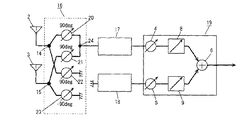
次に、図8を用いて、偶モード奇モード分波回路16の具体的な実現方法を示す。
Next, a specific method for realizing the even-mode odd-
図8において、偶モード奇モード分波回路16は、第1アンテナエレメント2と電気的に接続された第1給電ポート14と、第2アンテナエレメント3と電気的に接続された第2給電ポート15と、第1給電ポート14に電気的に接続されると共に移相量が90度の第1移相器20と、第1給電ポート14に電気的に接続されると共に移相量が90度の第3移相器22と、第2給電ポート15に電気的に接続されると共に移相量が90度の第2移相器21と、第2給電ポート15に電気的に接続されると共に移相量が−90度の第4移相器23と、第1移相器20と第2移相器21とが電気的に接続された第1交点24と、第3移相器22と第4移相器23とが電気的に接続された第2交点25とを備えている。そして、第1交点24は第1チューナ17と電気的に接続されており、第2交点25は第2チューナ18と電気的に接続されている。
In FIG. 8, the even-mode odd-
図8においては、第1交点24から給電した場合、第1給電ポート14と第2給電ポート15とは偶モードで給電され、第2交点25から給電した場合、第1給電ポート14と第2給電ポート15とは奇モードで給電されたこととなる。
In FIG. 8, when power is supplied from the
第1交点24から給電した場合、それぞれ、移相量が90度の第1移相器20と、第2移相器21とを介して、第1給電ポート14と第2給電ポート15とに到達するため、第1給電ポート14と第2給電ポート15の電圧は概ね同電位となる。そのため、第2交点25においては、それぞれ、移相量90度の第3移相器22と、移相量−90度の第4移相器23とを介した後、逆電位で足しあわされることとなる。すなわち、第2交点25は、常に概ね零電位となり、接地されているように見える。
When power is supplied from the
よって、第1交点24から入力された信号は、第2交点25の給電点には影響を及ぼさないと共に、第1給電ポート14と第2給電ポート15とに発生する偶モードの信号は、第2交点25には概ね現れない事となる。
Therefore, the signal input from the
上記の通り、第2交点25が接地されていることと等価であることから、図9のように表せる。図9に示したように、第1給電ポート14と第2給電ポート15とは、それぞれ、90度、−90度の移相器を介してグランドに接地されている事となる。よって、この構成がショートスタブとして動作し、第1給電ポート14から第2交点側と、第2給電ポート15から第2交点側とは開放状態として見え、図10に示す回路と等価と言える。
As described above, since this is equivalent to the
以上より、第1給電ポート14と第2給電ポート15とに偶モードの信号が供給された場合には、第1給電ポート14から第2交点25側と、第2給電ポート15から第2交点25側とは開放状態のように見え、第2交点25側へは信号が入力されないこととなる。
As described above, when an even mode signal is supplied to the first
次に、第2交点25から給電した場合、それぞれ、移相量90度の第3移相器22と、移相量−90度の第4移相器23とを介して、第1給電ポート14と第2給電ポート15とに到達するため、第1給電ポート14と第2給電ポート15の電圧は逆電位になる。そのため、第1交点24においては、それぞれ、移相量90度の第1移相器20と第2移相器21とを介した後、逆電位で足しあわされることとなる。すなわち、第1交点24は、常に概ね零電位となり、接地されているように見える。
Next, when power is supplied from the
よって、第2交点25から入力された信号は、第1交点24の給電点には影響を及ぼさないと共に、第1給電ポート14と第2給電ポート15とに発生する奇モードの信号は、第1交点24には概ね現れない事となる。
Therefore, the signal input from the
上記の通り、第1交点24が接地されていることと等価であることから、図11のように表せる。図11に示したように、第1給電ポート14と第2給電ポート15とは、それぞれ、90度、90度の移相器を介してグランドに接地されている事となる。よって、この構成がショートスタブとして動作し、第1給電ポート14から第1交点側と、第2給電ポート15から第1交点側とは開放状態として見え、図12に示す回路と等価と言える。
As described above, since this is equivalent to the
以上より、第1給電ポート14と第2給電ポート15とに奇モードの信号が供給された場合には、第1給電ポート14から第1交点24側と第2給電ポート15から第1交点24側とは開放状態のように見え、第1交点24側へは信号が入力されないこととなる。
As described above, when an odd mode signal is supplied to the first
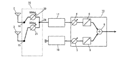
図8における偶モード奇モード分波回路16の位置ではなく、図13に示したように、第1チューナ17、第2チューナ18と、ダイバーシティ合成奇19との間に配置しても、同様の効果が期待できる。
Even if it is arranged between the
図8、又は、図13に示すように、信号処理部7(図示せず)により最適制御される第1可変移相器4、第2可変移相器5とをダイバーシティ合成器19が有するような、最大比合成方式または等利得合成方式のダイバーシティアンテナ装置においては、実質的に、偶モード奇モード分波回路16を削除しても(図14に示した構成としても)、図8や図13で示すダイバーシティアンテナ装置と同様の効果を得ることができる。
As shown in FIG. 8 or FIG. 13, the
以下、何故、このようなことが言えるかについて、図15を用いて説明する。 Hereinafter, why this can be said will be described with reference to FIG.
図15において、第1アンテナエレメント2の受信信号をx1(t)とし、第2アンテナエレメント3の受信信号をx2(t)とすると、x1(t)とx2(t)とは、それぞれ(数6)のように表される。
In FIG. 15, if the received signal of the
![]()
![]()
ここで、s1(t)は第1アンテナエレメント2の受信ベースバンド信号であり、s2(t)は第2アンテナエレメント3の受信ベースバンド信号である。また、fcはキャリア周波数である。
Here, s1 (t) is a reception baseband signal of the
第1チューナ17及び第2チューナ18において、キャリア周波数fcからベースバンドへ周波数変換されるため、第1チューナ17及び第2チューナ18の出力側においては、(数6)のexp(j*2*pi*fc*t)の項がなくなる。更に、偶モード奇モード分波回路16によって、ダイバーシティ合成器19の入力信号は、それぞれ、(数7)のように表される。
Since the frequency conversion from the carrier frequency fc to the baseband is performed in the
![]()
![]()
(数7)に示した二つの信号によって、ダイバーシティ合成が行われる。 Diversity combining is performed by the two signals shown in (Expression 7).
第1可変移相器4と第1可変増幅器8のダイバーシティ最適化後の重み付けの総和がαであったとし、第2可変移相器5と第2可変増幅器9のダイバーシティ最適化後の重み付けの総和がβであったとすると、合成器6からの出力信号は、(数8)のように表される。
Assume that the sum of the weights after the diversity optimization of the first variable phase shifter 4 and the first
ここで、偶モード奇モード分波回路16がない場合の合成器6からの出力信号を、図16を用いて考えてみる。
Here, the output signal from the synthesizer 6 when there is no even-mode odd-
図16において、第1アンテナエレメント2の受信信号をx1(t)とし、第2アンテナエレメント3の受信信号をx2(t)とすると、x1(t)とx2(t)とは、それぞれ(数6)と同様に表される。
In FIG. 16, when the received signal of the
そして、図15の場合と同様に、第1チューナ17及び第2チューナ18において、キャリア周波数fcからベースバンドへ周波数変換されるため、第1チューナ17及び第2チューナ18の出力側においては、(数6)のexp(j*2*pi*fc*t)の項がなくなる。
Similarly to the case of FIG. 15, the
よって、ダイバーシティ合成器19の入力信号は、それぞれs1(t)、s2(t)と表される。この二つの信号によって、ダイバーシティ合成が行われることとなる。
Therefore, the input signals of the
第1可変移相器4と第1可変増幅器8のダイバーシティ最適化後の重み付けの総和がα'であったとし、第2可変移相器5と第2可変増幅器9のダイバーシティ最適化後の重み付けの総和がβ'であったとすると、合成器6からの出力信号は、(数9)のように表される。
Assume that the sum of the weights after diversity optimization of the first variable phase shifter 4 and the first
![]()
![]()
すなわち、ダイバーシティ合成器19において、第1可変移相器8、第2可変移相器9、第1可変増幅器8、第2可変増幅器9の内、少なくとも1つが信号処理部7(図16においては便宜上、図示せず)により最適化されることにより、(数10)のように動作した場合、合成器6からの出力信号は、(数8)と同じものとなることが分かる。
That is, in the
![]()
![]()
故に、偶モード奇モード分波回路(または演算処理により偶モード奇モード分波回路を実現した場合は、その演算処理回路)は、削除しても同様の効果を得ることができる。 Therefore, even if the even-mode odd-mode demultiplexing circuit (or the arithmetic processing circuit when the even-mode odd-mode demultiplexing circuit is realized by arithmetic processing) is deleted, the same effect can be obtained.
なお、上記説明はシングルキャリアの場合で説明したが、OFDM(Orthogonal Frequency Division Multiplexing)のようなマルチキャリア信号の場合でも、同様な処理を行うことができる。 In addition, although the said description demonstrated in the case of a single carrier, the same process can be performed also in the case of a multicarrier signal like OFDM (Orthogonal Frequency Division Multiplexing).
また、特許請求の範囲における「第1アンテナエレメントの入力インピーダンス」とは(数1)、(数3)〜(数5)のS11のことであり、具体的には、第1アンテナエレメント2の給電点からアンテナ側を見た時のインピーダンス、または、偶モード奇モード分波回路16の第1給電ポート14からアンテナ側を見た時のインピーダンス、または、ダイバーシティ合成器19の第1可変移相器8の入力ポート(図示せず)からアンテナ側を見た時のインピーダンス等を表す。
The “input impedance of the first antenna element” in the claims is S11 in (Equation 1), (Equation 3) to (Equation 5). Impedance when viewing the antenna side from the feeding point, impedance when viewing the antenna side from the
同様に、特許請求の範囲における「第2アンテナエレメントの入力インピーダンス」とは(数1)、(数3)、(数4)のS22のことであり、具体的には、第2アンテナエレメント3の給電点からアンテナ側を見た時のインピーダンス、または、偶モード奇モード分波回路16の第2給電ポート15からアンテナ側を見た時のインピーダンス、または、ダイバーシティ合成器19の第2可変移相器9の入力ポート(図示せず)からアンテナ側を見た時のインピーダンス等を表す。
Similarly, the “input impedance of the second antenna element” in the claims refers to S22 of (Equation 1), (Equation 3), and (Equation 4). Specifically, the
なお、本発明に係るダイバーシティアンテナ装置と、このダイバーシティアンテナ装置の出力側に電気的に接続された表示部とを有した電子機器は、第1アンテナエレメント2と第2アンテナエレメント3とが近接した状態でありながら、上述した有利な効果が得られるダイバーシティアンテナを実現できるため、小型で且つ受信性能に優れた電子機器を実現できる。
In the electronic device having the diversity antenna device according to the present invention and a display unit electrically connected to the output side of the diversity antenna device, the
(実施の形態2)
以下、本発明の実施の形態2について、図17〜図26を用いて説明する。
(Embodiment 2)
The second embodiment of the present invention will be described below with reference to FIGS.
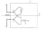
図17は、本発明のダイバーシティアンテナ装置の一例である。図1と同一部分に関しては、同一符号を付記し、説明を割愛する。 FIG. 17 is an example of the diversity antenna apparatus of the present invention. About the same part as FIG. 1, the same code | symbol is attached and description is omitted.
図17において、ダイバーシティアンテナ装置1を構成する第1アンテナエレメント2と第2アンテナエレメント3とは、任意面において概ね面対称、又は任意線において概ね線対称となることを特徴とする。尚、特許請求の範囲における「第1アンテナエレメントと第2アンテナエレメントは任意線において概ね線対称となる、又は、任意面において概ね面対称となり」は、それぞれのアンテナエレメントの電気長において、線対称または面対称であることを含んでいる。
In FIG. 17, the
本発明においては、図17のように、それぞれのアンテナエレメントが近接し、電磁結合している状態においても、良好なダイバーシティアンテナ装置の受信感度が得られる方式を提案する。 In the present invention, as shown in FIG. 17, a method is proposed in which good reception sensitivity of the diversity antenna apparatus can be obtained even when the antenna elements are close to each other and are electromagnetically coupled.
実施の形態1と同様、図18のように、第1アンテナエレメント2と第2アンテナエレメント3とを偶モード給電(図19中の第2給電部12が該当)と、奇モード給電(図19中の第1給電部11が該当)とをすることを考える。
As in the first embodiment, as shown in FIG. 18, the
まず、第1アンテナエレメント2と第2アンテナエレメント3とが、偶モード給電された場合について、図19を用いて説明する。
First, the case where the
図19において、第1アンテナエレメント2と第2アンテナエレメント3とが対称に構成されていることから、第1給電ポート14と第2給電ポート15とは同電位で給電されることとなる。すなわち、第1給電部11のプラス側、マイナス側が常に同電位になり、第2給電部12からの信号が第1給電部11へ流れ込まず、2つの給電部の間のアイソレーションが原理的に取れることが分かる。
In FIG. 19, since the
同様に、奇モード給電した場合を図20に示す。 Similarly, FIG. 20 shows a case where odd mode power feeding is performed.
この場合、第1アンテナエレメント2と第2アンテナエレメント3とが、対称に構成されていることから、第1給電ポート14と第2給電ポート15とは逆電位で給電されることとなる。すなわち、第2給電部12のプラス側は、第1給電ポート14と第2給電ポート15の合成電位となり、常に概ね零電位となる。故に、第1給電部11からの信号は、第2給電部12へは流れ込まず、2つの給電部間のアイソレーションは原理的に取れることが分かる。
In this case, since the
これより、第1アンテナエレメント2と第2アンテナエレメント3とを偶モード給電、奇モード給電することにより、2つの給電部は互いに影響を及ぼさないようすることができる。
As a result, even if the
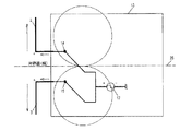
さらに、第1給電ポート14と第2給電ポート15とを偶モード給電した場合、各アンテナエレメント上の電流分布は図21に示したものとなる。つまり、対称面(線)28に概ね直交する電流は打ち消され、対称面(線)28に概ね平行な電流のみが放射に寄与する電流として残る形となる。その結果、放射パターンのピークは、対称面(線)28に概ね直交する方向を向く事となる。
Further, when the first
次に、第1給電ポート14と第2給電ポート15とを奇モード給電した場合、各アンテナエレメント上の電流分布は図22に示したものとなる。つまり、対称面(線)28に概ね平行な電流は打ち消され、対称面(線)28に概ね直交な電流のみが放射に寄与する電流として残る形となる。その結果、放射パターンのピークは、対称面(線)28に概ね平行な方向を向く事となる。
Next, when odd-mode power feeding is performed on the first
故に、これらを組み合わせると、図23のように、偶モード給電時と奇モード給電時のそれぞれの放射パターンのピーク方向は直交し、結果、本発明のダイバーシティアンテナ装置は二つの直交する偏波をもつこととなり、良好なダイバーシティ効果を得ることができる。 Therefore, when these are combined, as shown in FIG. 23, the peak directions of the radiation patterns at the even mode feeding and the odd mode feeding are orthogonal to each other. As a result, the diversity antenna apparatus of the present invention has two orthogonal polarizations. Therefore, a good diversity effect can be obtained.
なお、本発明の場合、実施の形態1と同様、偶モード奇モード分波回路16(または同様の効果を得るための演算処理を実施する演算処理回路)を、第1チューナ17、第2チューナ18の入力側または出力側に接続しても良い(図24、図25参照のこと)。
In the case of the present invention, as in the first embodiment, the even-mode odd-mode branching circuit 16 (or an arithmetic processing circuit that performs arithmetic processing for obtaining the same effect) is connected to the
また、ダイバーシティ合成方式として最大比合成方式または等利得合成方式を用いる場合、実施の形態1で説明した理由により、偶モード奇モード分波回路16(または同様の効果を得るための演算処理を実施する演算処理回路)を削除する事もできる。これにより、簡易にダイバーシティアンテナ装置を実現する事ができる。 Further, when the maximum ratio combining method or the equal gain combining method is used as the diversity combining method, the even-mode odd-mode branching circuit 16 (or arithmetic processing for obtaining the same effect is performed for the reason described in the first embodiment. Arithmetic processing circuit) can be deleted. Thereby, a diversity antenna device can be easily realized.
なお、第1アンテナエレメント2と第2アンテナエレメント3とを任意面に対して概ね面対称、又は任意線に対して概ね線対称とすることにより、図17〜図26に示した各アンテナエレメントの形状以外の形状であったとしても、偶モード給電時は対称面(線)28に概ね平行な偏波が、奇モード給電時は、対称面(線)28に概ね直交する偏波が生まれる。このため、本発明の特徴である「第1アンテナエレメント2と第2アンテナエレメント3とを任意面に対して概ね面対称、又は任意線に対して概ね線対称である」により、ダイバーシティアンテナ装置としては理想的な直交する2つの偏波を生成することができる。
The
なお、特許請求の範囲の「第1アンテナエレメントと第2アンテナエレメントのそれぞれの直線偏波が交差する点において、それぞれの直線偏波は所定の角度θを有しており、角度θ≠0度である」との記載は、互いに偏波が平行である場合には、偶・奇モードで給電しても、2つの偏波が得られないため、特許請求の範囲の請求項1、2から、この部分を削除するために記載した。 It should be noted that in the claims, each linearly polarized wave has a predetermined angle θ at the point where the linearly polarized waves of the first antenna element and the second antenna element intersect, and the angle θ ≠ 0 degrees. In the case where the polarizations are parallel to each other, two polarizations cannot be obtained even if power is supplied in the even / odd mode. Described to remove this part.
この具体的な状況を、図27を用いて説明する。図27において、第1アンテナエレメント2の偏波と第2アンテナエレメント3の偏波とが、共に、対称面(線)28に平行であった場合、奇モード給電しても、対称面(線)28に直交する偏波を生成する事が極めて困難であるため、2つの直交する偏波を生成する事が不可能となる。
This specific situation will be described with reference to FIG. In FIG. 27, when the polarization of the
よって、2つの直交する偏波が得られないため、特許請求の範囲の請求項1、2から、この部分を削除するための記載を追加した。
Therefore, since two orthogonal polarized waves cannot be obtained, a description for deleting this part is added from
なお、特許請求の範囲における「線対称」、「面対称」とは、構造上対称になっていなくても、電気的に対称になっていればその範囲に含まれ、同様な効果を得ることができる。 In addition, “line symmetry” and “plane symmetry” in the claims are included in the scope as long as they are electrically symmetrical, even if they are not symmetrical in structure, and the same effect can be obtained. Can do.
以上のように、本発明のダイバーシティアンテナ装置は、例えば、2本のモノポールアンテナのような小型なアンテナエレメント(それぞれのアンテナエレメントの偏波は直交及び平行ではない)を用いても、2つのモノポールアンテナの合成の放射パターンにおいては、給電のモード(偶モード及び奇モード)により直交する2つの偏波を得る事ができる。故に、最大比合成方式および等利得合成方式のダイバーシティ方式において、良好な受信特性を得る事ができ、小型の通信端末などに利用する事ができる。 As described above, the diversity antenna apparatus according to the present invention can use two small antenna elements such as two monopole antennas (the polarization of each antenna element is not orthogonal and parallel). In the combined radiation pattern of the monopole antenna, two orthogonal polarizations can be obtained depending on the feeding mode (even mode and odd mode). Therefore, in the diversity method of the maximum ratio combining method and the equal gain combining method, good reception characteristics can be obtained, and it can be used for a small communication terminal or the like.
1 ダイバーシティアンテナ装置
2 第1アンテナエレメント
3 第2アンテナエレメント
4 第1可変移相器
5 第2可変移相器
6 合成器
7 信号処理部
8 第1可変増幅器
9 第2可変増幅器
10 従来のダイバーシティアンテナ装置
11 第1給電部
12 第2給電部
13 グランド板
14 第1給電ポート
15 第2給電ポート
16 偶モード奇モード分波回路
17 第1チューナ
18 第2チューナ
19 ダイバーシティ合成器
20 第1移相器
21 第2移相器
22 第3移相器
23 第4位相器
24 第1交点
25 第2交点
28 対称面(線)
DESCRIPTION OF
Claims (5)
前記第1アンテナエレメントに電気的に接続された第1可変移相器と、
前記第2アンテナエレメントに電気的に接続された第2可変移相器と、
前記第1可変移相器の出力信号と前記第2可変移相器の出力信号とを合成する合成器と、
前記合成器の出力側に電気的に接続される信号処理部と、
前記第1可変位相器に直列に接続された第1可変増幅器と、
前記第2可変位相器に直列に接続された第2可変増幅器と、
を有し、
前記信号処理部は、前記信号処理部に入力される信号の信号品質値を導出し、この信号品質値に基づいて前記第1可変移相器と前記第2可変移相器の移相量を制御すると共に、
前記第1アンテナエレメントの入力インピーダンスと前記第2アンテナエレメントの入力インピーダンスとは概ね同一値であり、
前記第1アンテナエレメントと前記第2アンテナエレメントのそれぞれの偏波が共に直線偏波の場合は、
前記第1アンテナエレメントと前記第2アンテナエレメントのそれぞれの直線偏波が交差する点において、それぞれの直線偏波は所定の角度θを有しており、角度θ≠0度で且つ、θ≠90度であって、
前記信号処理部は、前記信号品質値に基づいて前記第1可変移相器の移相量と前記第2可変移相器の移相量と前記第1可変増幅器と前記第2可変増幅器の利得とを制御することにより、
直交する偏波から得られた2つの信号を前記合成器で合成することと同様の効果が得られるダイバーシティアンテナ装置。 A first antenna element; a second antenna element;
A first variable phase shifter electrically connected to the first antenna element;
A second variable phase shifter electrically connected to the second antenna element;
A combiner that combines the output signal of the first variable phase shifter and the output signal of the second variable phase shifter;
A signal processing unit electrically connected to the output side of the combiner ;
A first variable amplifier connected in series to the first variable phase shifter;
A second variable amplifier connected in series with the second variable phase shifter;
Have
The signal processing unit derives a signal quality value of a signal input to the signal processing unit, and calculates a phase shift amount between the first variable phase shifter and the second variable phase shifter based on the signal quality value. Control and
The input impedance of the first antenna element and the input impedance of the second antenna element are substantially the same value,
When the polarizations of the first antenna element and the second antenna element are both linearly polarized waves,
At the point where the linearly polarized waves of the first antenna element and the second antenna element intersect, the linearly polarized waves have a predetermined angle θ, the angle θ ≠ 0 degrees, and θ ≠ 90. What degree der,
The signal processing unit includes a phase shift amount of the first variable phase shifter, a phase shift amount of the second variable phase shifter, and gains of the first variable amplifier and the second variable amplifier based on the signal quality value. By controlling
A diversity antenna apparatus capable of obtaining the same effect as that obtained by combining two signals obtained from orthogonally polarized waves by the combiner .
前記第1アンテナエレメントに電気的に接続された第1可変移相器と、
前記第2アンテナエレメントに電気的に接続された第2可変移相器と、
前記第1可変移相器の出力信号と前記第2可変移相器の出力信号とを合成する合成器と、
前記合成器の出力側に電気的に接続される信号処理部と、
前記第1可変位相器に直列に接続された第1可変増幅器と、
前記第2可変位相器に直列に接続された第2可変増幅器と、
を有し、
前記信号処理部は、前記信号処理部に入力される信号の信号品質値を導出し、この信号品質値に基づいて前記第1可変移相器と前記第2可変移相器の移相量を制御すると共に、
前記第1アンテナエレメントと前記第2アンテナエレメントは任意線において概ね線対称となる、又は、任意面において概ね面対称となり、
前記第1アンテナエレメントと前記第2アンテナエレメントのそれぞれの偏波が共に直線偏波の場合は、
前記第1アンテナエレメントと前記第2アンテナエレメントのそれぞれの直線偏波が交差する点において、それぞれの直線偏波は所定の角度θを有しており、
角度θ≠0度で且つ、θ≠90度であって、
前記信号処理部は、前記信号品質値に基づいて前記第1可変移相器の移相量と前記第2可変移相器の移相量と前記第1可変増幅器と前記第2可変増幅器の利得とを制御することにより、
直交する偏波から得られた2つの信号を前記合成器で合成することと同様の効果が得られるダイバーシティアンテナ装置。 A first antenna element; a second antenna element;
A first variable phase shifter electrically connected to the first antenna element;
A second variable phase shifter electrically connected to the second antenna element;
A combiner that combines the output signal of the first variable phase shifter and the output signal of the second variable phase shifter;
A signal processing unit electrically connected to the output side of the combiner ;
A first variable amplifier connected in series to the first variable phase shifter;
A second variable amplifier connected in series with the second variable phase shifter;
Have
The signal processing unit derives a signal quality value of a signal input to the signal processing unit, and calculates a phase shift amount between the first variable phase shifter and the second variable phase shifter based on the signal quality value. Control and
The first antenna element and the second antenna element are substantially line symmetric in an arbitrary line, or are generally plane symmetric in an arbitrary plane,
When the polarizations of the first antenna element and the second antenna element are both linearly polarized waves,
Each linearly polarized wave has a predetermined angle θ at a point where the linearly polarized waves of the first antenna element and the second antenna element intersect each other.
And at an angle θ ≠ 0 degrees, it θ ≠ 90 degrees der,
The signal processing unit includes a phase shift amount of the first variable phase shifter, a phase shift amount of the second variable phase shifter, and gains of the first variable amplifier and the second variable amplifier based on the signal quality value. By controlling
A diversity antenna apparatus capable of obtaining the same effect as that obtained by combining two signals obtained from orthogonally polarized waves by the combiner .
直交する偏波から得られた2つの信号を前記合成器で合成することと同様の効果が得られる、請求項1又は請求項2のいずれかに記載のダイバーシティアンテナ装置。 The signal processing unit controls the amount of phase shift of the first variable phase shifter and the second variable phase shifter so that the signal quality value is the best ,
The diversity antenna device according to claim 1 , wherein an effect similar to that of combining two signals obtained from orthogonal polarizations by the combiner is obtained .
直交する偏波から得られた2つの信号を前記合成器で合成することと同様の効果が得られる請求項3に記載のダイバーシティアンテナ装置。 The signal processing unit controls the gain of the first variable amplifier and the second variable amplifier so that the signal quality value is the best ,
The diversity antenna device according to claim 3, wherein an effect similar to that obtained by combining two signals obtained from orthogonally polarized waves by the combiner is obtained .
前記ダイバーシティアンテナ装置の出力側に電気的に接続された表示部とを有した電子機器。 The diversity antenna device according to claim 1 or 2,
An electronic apparatus having a display unit electrically connected to an output side of the diversity antenna device.
Priority Applications (3)
| Application Number | Priority Date | Filing Date | Title |
|---|---|---|---|
| JP2008265984A JP5380997B2 (en) | 2008-10-15 | 2008-10-15 | Diversity antenna device and electronic device using the same |
| EP09172540.8A EP2178170B1 (en) | 2008-10-15 | 2009-10-08 | Diversity antenna system and electronic apparatus using the same |
| CN200910207309A CN101728626A (en) | 2008-10-15 | 2009-10-15 | Diversity antenna system and electronic apparatus |
Applications Claiming Priority (1)
| Application Number | Priority Date | Filing Date | Title |
|---|---|---|---|
| JP2008265984A JP5380997B2 (en) | 2008-10-15 | 2008-10-15 | Diversity antenna device and electronic device using the same |
Publications (2)
| Publication Number | Publication Date |
|---|---|
| JP2010098411A JP2010098411A (en) | 2010-04-30 |
| JP5380997B2 true JP5380997B2 (en) | 2014-01-08 |
Family
ID=41728371
Family Applications (1)
| Application Number | Title | Priority Date | Filing Date |
|---|---|---|---|
| JP2008265984A Expired - Fee Related JP5380997B2 (en) | 2008-10-15 | 2008-10-15 | Diversity antenna device and electronic device using the same |
Country Status (3)
| Country | Link |
|---|---|
| EP (1) | EP2178170B1 (en) |
| JP (1) | JP5380997B2 (en) |
| CN (1) | CN101728626A (en) |
Cited By (1)
| Publication number | Priority date | Publication date | Assignee | Title |
|---|---|---|---|---|
| US10218426B1 (en) | 2017-09-11 | 2019-02-26 | Kabushiki Kaisha Toshiba | Antenna device, wireless communication device and signal transmission method |
Families Citing this family (5)
| Publication number | Priority date | Publication date | Assignee | Title |
|---|---|---|---|---|
| JP5423895B2 (en) * | 2010-07-06 | 2014-02-19 | パナソニック株式会社 | Antenna device and display device |
| US20140225805A1 (en) * | 2011-03-15 | 2014-08-14 | Helen K. Pan | Conformal phased array antenna with integrated transceiver |
| US8849217B2 (en) | 2011-06-22 | 2014-09-30 | Broadcom Corporation | Antenna arrangement |
| GB2492122A (en) * | 2011-06-22 | 2012-12-26 | Renesas Mobile Corp | Diversity antenna system with de-correlation apparatus and method |
| KR20160015387A (en) | 2014-04-22 | 2016-02-12 | 후아웨이 디바이스 컴퍼니 리미티드 | Antenna system and terminal |
Family Cites Families (8)
| Publication number | Priority date | Publication date | Assignee | Title |
|---|---|---|---|---|
| GB2291271B (en) * | 1994-07-09 | 1998-05-13 | Northern Telecom Ltd | Communications antenna structure |
| JP2004242159A (en) * | 2003-02-07 | 2004-08-26 | Ngk Spark Plug Co Ltd | High frequency antenna module |
| KR100631668B1 (en) | 2003-05-13 | 2006-10-09 | 엘지전자 주식회사 | Mobile station reception diversity apparatus and method in high speed data transmission method mobile communication system |
| GB0311361D0 (en) | 2003-05-19 | 2003-06-25 | Antenova Ltd | Dual band antenna system with diversity |
| JP4645061B2 (en) * | 2004-05-11 | 2011-03-09 | ブラザー工業株式会社 | Wireless tag communication device |
| JP2005318407A (en) * | 2004-04-30 | 2005-11-10 | Matsushita Electric Ind Co Ltd | Mobile phone with broadcast receiver |
| US8457582B2 (en) * | 2006-03-15 | 2013-06-04 | Panasonic Corporation | Adaptive control apparatus using multiple adaptive control methods |
| WO2009113307A1 (en) * | 2008-03-13 | 2009-09-17 | パナソニック株式会社 | Signal branching filter, electronic device using the same, antenna apparatus, and signal transmission system used in all of the above |
-
2008
- 2008-10-15 JP JP2008265984A patent/JP5380997B2/en not_active Expired - Fee Related
-
2009
- 2009-10-08 EP EP09172540.8A patent/EP2178170B1/en not_active Not-in-force
- 2009-10-15 CN CN200910207309A patent/CN101728626A/en active Pending
Cited By (1)
| Publication number | Priority date | Publication date | Assignee | Title |
|---|---|---|---|---|
| US10218426B1 (en) | 2017-09-11 | 2019-02-26 | Kabushiki Kaisha Toshiba | Antenna device, wireless communication device and signal transmission method |
Also Published As
| Publication number | Publication date |
|---|---|
| EP2178170A1 (en) | 2010-04-21 |
| EP2178170B1 (en) | 2014-10-01 |
| CN101728626A (en) | 2010-06-09 |
| JP2010098411A (en) | 2010-04-30 |
Similar Documents
| Publication | Publication Date | Title |
|---|---|---|
| JP4695210B2 (en) | Method and apparatus for coupling elimination of closely spaced antennas | |
| JP5380997B2 (en) | Diversity antenna device and electronic device using the same | |
| JP5381150B2 (en) | Diversity antenna device and electronic device using the same | |
| US7292195B2 (en) | Energy diversity antenna and system | |
| US7460071B2 (en) | Triple polarized patch antenna | |
| CN111987432A (en) | Antenna structures and electronics | |
| WO2008001384A1 (en) | Multi-antenna system for differential wireless communication devices | |
| TWI813371B (en) | Rf receiver and method for receiving rf input signal | |
| JPWO2014061381A1 (en) | Decoupling circuit | |
| CN101091289A (en) | Triple Polarized Slot Antenna | |
| JP2014093767A (en) | Orthogonal polarization sharing and polarization surface variable antenna | |
| Ivrlac et al. | Transmit and receive array gain of uniform linear arrays of isotrops | |
| US9755601B1 (en) | Wireless receiver having improved phase shifting schemes with reduced number of phase shifters | |
| JP5338814B2 (en) | ANTENNA DEVICE AND COMMUNICATION DEVICE USING THE SAME | |
| Ryu et al. | Design and beamforming performance of the compact ESPAR antenna for the beam space MIMO system | |
| JP2005198102A (en) | Antenna device and radio device | |
| JP2011023931A (en) | Antenna device, and electronic apparatus using the same |
Legal Events
| Date | Code | Title | Description |
|---|---|---|---|
| A621 | Written request for application examination |
Free format text: JAPANESE INTERMEDIATE CODE: A621 Effective date: 20111006 |
|
| RD01 | Notification of change of attorney |
Free format text: JAPANESE INTERMEDIATE CODE: A7421 Effective date: 20111114 |
|
| A977 | Report on retrieval |
Free format text: JAPANESE INTERMEDIATE CODE: A971007 Effective date: 20121024 |
|
| RD01 | Notification of change of attorney |
Free format text: JAPANESE INTERMEDIATE CODE: A7421 Effective date: 20121214 |
|
| A131 | Notification of reasons for refusal |
Free format text: JAPANESE INTERMEDIATE CODE: A131 Effective date: 20130402 |
|
| A521 | Written amendment |
Free format text: JAPANESE INTERMEDIATE CODE: A523 Effective date: 20130603 |
|
| TRDD | Decision of grant or rejection written | ||
| A01 | Written decision to grant a patent or to grant a registration (utility model) |
Free format text: JAPANESE INTERMEDIATE CODE: A01 Effective date: 20130903 |
|
| A61 | First payment of annual fees (during grant procedure) |
Free format text: JAPANESE INTERMEDIATE CODE: A61 Effective date: 20130916 |
|
| LAPS | Cancellation because of no payment of annual fees |