JP5369552B2 - Pixel circuit driving method, light emitting device, and electronic apparatus - Google Patents
Pixel circuit driving method, light emitting device, and electronic apparatus Download PDFInfo
- Publication number
- JP5369552B2 JP5369552B2 JP2008226735A JP2008226735A JP5369552B2 JP 5369552 B2 JP5369552 B2 JP 5369552B2 JP 2008226735 A JP2008226735 A JP 2008226735A JP 2008226735 A JP2008226735 A JP 2008226735A JP 5369552 B2 JP5369552 B2 JP 5369552B2
- Authority
- JP
- Japan
- Prior art keywords
- period
- potential
- pixel circuit
- driving transistor
- gate
- Prior art date
- Legal status (The legal status is an assumption and is not a legal conclusion. Google has not performed a legal analysis and makes no representation as to the accuracy of the status listed.)
- Expired - Fee Related
Links
- 238000000034 method Methods 0.000 title claims description 36
- 239000003990 capacitor Substances 0.000 claims abstract description 84
- 230000008859 change Effects 0.000 claims description 19
- 238000013459 approach Methods 0.000 claims description 13
- 238000010586 diagram Methods 0.000 description 16
- 101100351213 Chromobacterium violaceum (strain ATCC 12472 / DSM 30191 / JCM 1249 / NBRC 12614 / NCIMB 9131 / NCTC 9757) pcp gene Proteins 0.000 description 13
- 101100126615 Mus musculus Itpr1 gene Proteins 0.000 description 13
- 101150075058 pcp1 gene Proteins 0.000 description 13
- 101001098880 Homo sapiens Purkinje cell protein 2 homolog Proteins 0.000 description 11
- 102100028516 Receptor-type tyrosine-protein phosphatase U Human genes 0.000 description 11
- 230000008901 benefit Effects 0.000 description 8
- 230000000694 effects Effects 0.000 description 8
- 230000007423 decrease Effects 0.000 description 7
- 230000004048 modification Effects 0.000 description 7
- 238000012986 modification Methods 0.000 description 7
- 230000007704 transition Effects 0.000 description 3
- 230000009471 action Effects 0.000 description 2
- 230000001413 cellular effect Effects 0.000 description 2
- 238000005401 electroluminescence Methods 0.000 description 2
- 239000011159 matrix material Substances 0.000 description 2
- 238000004904 shortening Methods 0.000 description 2
- 230000002123 temporal effect Effects 0.000 description 2
- 239000010409 thin film Substances 0.000 description 2
- 230000000052 comparative effect Effects 0.000 description 1
- 230000003247 decreasing effect Effects 0.000 description 1
- 239000010408 film Substances 0.000 description 1
- 239000000463 material Substances 0.000 description 1
- 230000003287 optical effect Effects 0.000 description 1
- 239000000758 substrate Substances 0.000 description 1
Images


Landscapes
- Electroluminescent Light Sources (AREA)
- Control Of Indicators Other Than Cathode Ray Tubes (AREA)
- Control Of El Displays (AREA)
Abstract
Description
本発明は、有機EL(Electroluminescence)素子などの発光素子を駆動する技術に関する。 The present invention relates to a technique for driving a light emitting element such as an organic EL (Electroluminescence) element.
発光素子に供給される駆動電流の電流量を駆動トランジスタが制御する発光装置においては、駆動トランジスタや発光素子の電気的な特性の誤差(目標値からの相違や各素子間のバラツキ)が問題となる。特許文献1には、駆動トランジスタのゲート−ソース間に介在する保持容量の両端間の電圧を、駆動トランジスタの閾値電圧に設定してから階調値に応じた電圧に変化させることで、駆動トランジスタの閾値電圧および移動度の誤差(ひいては駆動電流の電流量の誤差)を補償する技術が開示されている。
しかし、特許文献1の技術で駆動電流の誤差が有効に補償されるのは特定の階調値が指定された場合に限定され、階調値によっては駆動電流の誤差を解消できない場合がある。以上の事情に鑑みて、本発明は、複数の階調値について駆動電流の誤差を抑制することを目的とする。
However, the error of the drive current is effectively compensated by the technique of
以上の課題を解決するために、本発明の第1の態様に係る画素回路の駆動方法は、相互に直列に接続された発光素子および駆動トランジスタと、発光素子と駆動トランジスタとの間の経路と駆動トランジスタのゲートとの間に介在する保持容量とを含む画素回路を駆動する方法であって、駆動トランジスタを導通させるとともに当該駆動トランジスタのゲートに基準電位(例えば基準電位VREF)を供給することで保持容量の両端間の電圧を駆動トランジスタの閾値電圧に漸近させる第1補償動作を補償期間において実行し、補償期間の経過後の書込期間において、駆動トランジスタのゲートの電位を、当該画素回路に指定された階調値に応じた階調電位に変化させるとともに、保持容量の両端間の電圧を駆動トランジスタの閾値電圧に漸近させる第2補償動作を、当該階調値に応じて可変に設定された時間長(例えば時間長tb)にわたって実行し、書込期間の経過後の駆動期間において、駆動トランジスタのゲートに対する電位の供給を停止することで、保持容量の両端間の電圧に応じた駆動電流を発光素子に供給する。以上の駆動方法においては、第2補償動作の時間長が階調値(あるいは階調電位)に応じて可変に設定されるから、複数の階調値について駆動電流の誤差を有効に抑制することが可能である。 In order to solve the above problems, a driving method of a pixel circuit according to a first aspect of the present invention includes a light emitting element and a driving transistor connected in series with each other, a path between the light emitting element and the driving transistor, and A method of driving a pixel circuit including a storage capacitor interposed between a gate of a driving transistor and supplying a reference potential (for example, a reference potential VREF) to the gate of the driving transistor while making the driving transistor conductive. A first compensation operation for causing the voltage across the storage capacitor to gradually approach the threshold voltage of the driving transistor is executed in the compensation period, and the gate potential of the driving transistor is applied to the pixel circuit in the writing period after the compensation period has elapsed. While changing the gradation potential according to the specified gradation value, the voltage across the storage capacitor is asymptotic to the threshold voltage of the drive transistor. The second compensation operation is performed over a time length (eg, time length tb) variably set according to the gradation value, and the potential is supplied to the gate of the driving transistor in the driving period after the writing period has elapsed. Is stopped, a drive current corresponding to the voltage across the storage capacitor is supplied to the light emitting element. In the above driving method, since the time length of the second compensation operation is variably set according to the gradation value (or gradation potential), it is possible to effectively suppress the drive current error for a plurality of gradation values. Is possible.
さらに詳述すると、書込期間において階調電位を供給したときの保持容量の両端間の電圧の変化量(例えば電圧VIN)が大きいほど、駆動電流の誤差を抑制できる第2補償動作の時間長が短くなるという傾向を前提とすれば、書込期間において階調電位を供給したときの保持容量の両端間の電圧の変化量(例えば電圧VIN)が大きいほど第2補償動作の時間長が短くなるように、当該画素回路に指定された階調値に応じて第2補償動作の時間長を可変に設定する。例えば、書込期間において階調電位を供給したときの保持容量の両端間の電圧の変化量と第2補償動作の時間長との乗算値が所定値に近づくように、当該画素回路に指定された階調値に応じて第2補償動作の時間長を可変に設定する。 More specifically, the time length of the second compensation operation in which the error of the drive current can be suppressed as the amount of change in voltage between the two ends of the storage capacitor when the gradation potential is supplied in the writing period (for example, the voltage VIN) is increased. Assuming the tendency to decrease, the time length of the second compensation operation becomes shorter as the amount of change in voltage across the storage capacitor (for example, voltage VIN) when the gradation potential is supplied in the writing period is larger. As described above, the time length of the second compensation operation is variably set in accordance with the gradation value designated for the pixel circuit. For example, the pixel circuit is designated such that the multiplication value of the amount of change in the voltage across the storage capacitor when the gradation potential is supplied during the writing period and the time length of the second compensation operation approaches a predetermined value. The time length of the second compensation operation is variably set according to the gradation value.
ところで、階調値が小さいほど、駆動電流の誤差が抑制される第2補償動作の時間長が長くなるという傾向のもとで、階調値が小さい場合にも駆動電流の誤差を最小化しようとすれば、過度に長い時間長を第2補償動作のために確保する必要がある。そこで、本発明の好適な態様においては、階調値が所定値を下回る場合に、第2補償動作の時間長を、階調値に依存しない所定値(例えば図10の時間長tmax)に設定する(すなわち、第2補償動作の時間長に上限を設定する)。以上の駆動方法によれば、階調値が小さい場合にも第2補償動作の時間長が適度な長さに抑制されるという利点がある。 By the way, the smaller the gradation value, the longer the time length of the second compensation operation in which the drive current error is suppressed, so that the drive current error is minimized even when the gradation value is small. If so, it is necessary to ensure an excessively long time length for the second compensation operation. Therefore, in a preferred aspect of the present invention, when the gradation value is lower than the predetermined value, the time length of the second compensation operation is set to a predetermined value that does not depend on the gradation value (for example, the time length tmax in FIG. 10). (That is, an upper limit is set for the time length of the second compensation operation). The above driving method has an advantage that the time length of the second compensation operation is suppressed to an appropriate length even when the gradation value is small.
本発明の好適な態様において、補償期間では、保持容量の両端間の電圧を、第1補償動作によって駆動トランジスタの閾値電圧に設定する。以上の態様においては、駆動トランジスタの閾値電圧の誤差が第1補償動作で正確に補償されるという利点がある。以上の態様の具体例は、例えば第1実施形態として後述される。なお、保持容量の両端間の電圧が駆動トランジスタの閾値電圧に完全に合致するためには論理上は無限の時間長が必要となるから、本発明において「保持容量の両端間の電圧を駆動トランジスタの閾値電圧に設定する」とは、保持容量の両端間の電圧が駆動トランジスタの閾値電圧に充分に接近した状態(実質的に閾値電圧に到達した状態)を意味する。 In a preferred aspect of the present invention, in the compensation period, the voltage across the storage capacitor is set to the threshold voltage of the driving transistor by the first compensation operation. In the above aspect, there is an advantage that the error of the threshold voltage of the driving transistor is accurately compensated by the first compensation operation. A specific example of the above aspect will be described later as the first embodiment, for example. Note that in order for the voltage across the storage capacitor to completely match the threshold voltage of the drive transistor, an infinite time length is logically required. "Set to the threshold voltage of" means a state in which the voltage across the storage capacitor is sufficiently close to the threshold voltage of the driving transistor (a state in which the threshold voltage is substantially reached).
本発明の別の態様において、補償期間では、階調値に応じて可変に設定された時間長(例えば図17の時間長t1)にわたって第1補償動作を実行する。以上の態様においては、第1補償動作および第2補償動作の双方の時間長が階調値に応じて可変に設定されるから、第1補償動作の時間長のみを調整する場合と比較して広い範囲にわたる階調値について駆動電流の誤差を抑制することが可能である。なお、以上の態様の具体例は第4実施形態として後述される。 In another aspect of the present invention, in the compensation period, the first compensation operation is performed over a time length that is variably set according to the gradation value (for example, the time length t1 in FIG. 17). In the above aspect, since the time lengths of both the first compensation operation and the second compensation operation are variably set according to the gradation value, compared with the case where only the time length of the first compensation operation is adjusted. It is possible to suppress an error in the drive current for gradation values over a wide range. In addition, the specific example of the above aspect is later mentioned as 4th Embodiment.
本発明の第2の態様に係る画素回路の駆動方法は、複数の画素回路の各々について、当該画素回路に指定された階調値に応じた階調電位を信号線から当該画素回路の駆動トランジスタのゲートに供給することで、保持容量の両端間の電圧を駆動トランジスタの閾値電圧に漸近させる第2補償動作を、第1期間(例えば図14の期間h1)と第2期間(例えば図14の期間h2)とを各々が含む複数の単位期間のうち当該画素回路に対応する単位期間の第2期間において、当該階調値に応じて可変に設定された時間長にわたって実行する一方、駆動トランジスタを導通させるとともに駆動トランジスタのゲートに信号線から基準電位を供給することで保持容量の両端間の電圧を駆動トランジスタの閾値電圧に漸近させる第1補償動作を、当該画素回路に対応する単位期間の第2期間の開始前の2以上の第1期間において間欠的に実行し、当該画素回路に対応する単位期間の第2期間の経過後に、当該画素回路の駆動トランジスタのゲートに対する電位の供給を停止することで、保持容量の両端間の電圧に応じた駆動電流を発光素子に供給する。 In the pixel circuit driving method according to the second aspect of the present invention, for each of the plurality of pixel circuits, a gradation potential corresponding to a gradation value designated for the pixel circuit is supplied from the signal line to the driving transistor of the pixel circuit. Is supplied to the gate of the storage capacitor, the second compensation operation for making the voltage across the storage capacitor asymptotically approach the threshold voltage of the driving transistor is performed in the first period (for example, period h1 in FIG. 14) and the second period (for example, in FIG. 14). Among the plurality of unit periods each including the period h2), the second period of the unit period corresponding to the pixel circuit is executed over a time length variably set according to the gradation value, A first compensation operation for making the pixel asymptotically close to the threshold voltage of the drive transistor by conducting the voltage and supplying a reference potential from the signal line to the gate of the drive transistor as the reference voltage is applied to the pixel of the drive transistor. Intermittently executed in two or more first periods before the start of the second period of the unit period corresponding to the path, and after the second period of the unit period corresponding to the pixel circuit has elapsed, the drive transistor of the pixel circuit By stopping the supply of the potential to the gate, a driving current corresponding to the voltage across the storage capacitor is supplied to the light emitting element.
第2の態様においては、第2補償動作の時間長が階調値(あるいは階調電位)に応じて可変に設定されるから、第1の態様に係る駆動方法と同様に、複数の階調値について駆動電流の誤差を有効に抑制することが可能である。さらに、複数の単位期間の第1期間にわたって第1補償動作が間欠的に実行されるから、保持容量の両端間の電圧を第1補償動作で駆動トランジスタの閾値電圧に充分に接近させることができる。なお、以上の駆動方法の具体例は、例えば第2実施形態として後述される。また、共通の信号線が基準電位の供給と階調電位の供給とに兼用されるから、基準電位と階調電位とが別個の配線で各画素回路に供給される構成と比較して、画素回路の構成が簡素化されるという利点もある。なお、第1期間と第2期間との先後および比率や第1補償動作を実行する単位期間の個数は本発明において任意である。 In the second aspect, since the time length of the second compensation operation is variably set according to the gradation value (or gradation potential), a plurality of gradations are provided as in the driving method according to the first aspect. It is possible to effectively suppress the error of the drive current with respect to the value. Furthermore, since the first compensation operation is intermittently performed over the first period of the plurality of unit periods, the voltage across the storage capacitor can be made sufficiently close to the threshold voltage of the driving transistor by the first compensation operation. . A specific example of the above driving method will be described later as a second embodiment, for example. In addition, since the common signal line is used for both the supply of the reference potential and the supply of the gradation potential, the pixel potential is compared with the configuration in which the reference potential and the gradation potential are supplied to each pixel circuit through separate wirings. There is also an advantage that the configuration of the circuit is simplified. It should be noted that the preceding and following ratios of the first period and the second period and the number of unit periods for executing the first compensation operation are arbitrary in the present invention.
本発明の第3の態様に係る画素回路の駆動方法は、複数の画素回路の各々について、当該画素回路に指定された階調値に応じた階調電位を信号線から当該画素回路の駆動トランジスタのゲートに供給することで、保持容量の両端間の電圧を駆動トランジスタの閾値電圧に漸近させる第2補償動作を、複数の単位期間のうち当該画素回路に対応する単位期間において、当該階調値に応じて可変に設定された時間長にわたって実行する一方、駆動トランジスタを導通させるとともに駆動トランジスタのゲートに給電線(例えば図15の給電線54)から基準電位を供給することで保持容量の両端間の電圧を駆動トランジスタの閾値電圧に漸近させる第1補償動作を、当該画素回路に対応する単位期間の開始前の2以上の単位期間にわたって実行し、当該画素回路に対応する単位期間の経過後に、当該画素回路の駆動トランジスタのゲートに対する電位の供給を停止することで、保持容量の両端間の電圧に応じた駆動電流を発光素子に供給する。
In the pixel circuit driving method according to the third aspect of the present invention, for each of the plurality of pixel circuits, a gradation potential corresponding to a gradation value designated for the pixel circuit is supplied from the signal line to the driving transistor of the pixel circuit. The second compensation operation for gradually bringing the voltage across the storage capacitor close to the threshold voltage of the driving transistor by supplying the voltage to the gate of the storage capacitor in the unit period corresponding to the pixel circuit among the plurality of unit periods While the drive transistor is turned on and the reference potential is supplied to the gate of the drive transistor from a power supply line (for example, the
第3の態様においては、第2補償動作の時間長が階調値(あるいは階調電位)に応じて可変に設定されるから、第1の態様に係る駆動方法と同様に、複数の階調値について駆動電流の誤差を有効に抑制することが可能である。さらに、複数の単位期間の第1期間にわたって第1補償動作が間欠的に実行されるから、保持容量の両端間の電圧を第1補償動作で駆動トランジスタの閾値電圧に充分に接近させることができる。また、第2補償動作の時間長を最長で単位期間の全体の時間長まで設定できる(第2補償動作の時間長の変化幅を充分に確保できる)という利点もある。なお、第1補償動作を実行する単位期間の個数は本発明において任意である。 In the third aspect, since the time length of the second compensation operation is variably set according to the gradation value (or gradation potential), a plurality of gradations are provided as in the driving method according to the first aspect. It is possible to effectively suppress the error of the drive current with respect to the value. Furthermore, since the first compensation operation is intermittently performed over the first period of the plurality of unit periods, the voltage across the storage capacitor can be made sufficiently close to the threshold voltage of the driving transistor by the first compensation operation. . In addition, there is an advantage that the time length of the second compensation operation can be set up to the entire time length of the unit period (a change width of the time length of the second compensation operation can be sufficiently secured). In the present invention, the number of unit periods for executing the first compensation operation is arbitrary.
なお、第1の態様に係る画素回路の駆動方法において、第1補償動作が複数の単位期間にて実行されるか1個の単位期間にて実行されるか(補償期間が複数の単位期間にわたるか1個の単位期間に包含されるか)は不問であるから、第2の態様および第3の態様に係る駆動方法は、第1の態様に係る駆動方法の範囲に包含される。 In the pixel circuit driving method according to the first aspect, whether the first compensation operation is performed in a plurality of unit periods or in one unit period (the compensation period extends over a plurality of unit periods). Therefore, the driving method according to the second aspect and the third aspect is included in the range of the driving method according to the first aspect.
本発明の第1の態様に係る発光装置は、相互に直列に接続された発光素子および駆動トランジスタと、発光素子と駆動トランジスタとの間の経路と駆動トランジスタのゲートとの間に介在する保持容量とを含む画素回路と、本発明の第1の態様に係る駆動方法を実行する駆動回路とを具備する。第1の態様に係る発光装置によれば、第1の態様に係る駆動方法と同様の効果が実現される。 A light emitting device according to a first aspect of the present invention includes a light emitting element and a driving transistor connected in series with each other, and a storage capacitor interposed between a path between the light emitting element and the driving transistor and a gate of the driving transistor. And a driving circuit that executes the driving method according to the first aspect of the present invention. According to the light emitting device according to the first aspect, the same effect as the driving method according to the first aspect is realized.
本発明の第2の態様に係る発光装置は、相互に直列に接続された発光素子および駆動トランジスタと、発光素子と駆動トランジスタとの間の経路と駆動トランジスタのゲートとの間に介在する保持容量とを各々が含む複数の画素回路と、本発明の第2の態様に係る駆動方法を実行する駆動回路とを具備する。第2の態様に係る発光装置によれば、第2の態様に係る駆動方法と同様の効果が実現される。 A light emitting device according to a second aspect of the present invention includes a light emitting element and a driving transistor connected in series with each other, and a storage capacitor interposed between a path between the light emitting element and the driving transistor and a gate of the driving transistor. And a driving circuit that executes the driving method according to the second aspect of the present invention. According to the light emitting device according to the second aspect, an effect similar to that of the driving method according to the second aspect is realized.
第2の態様に係る発光装置の具体例において、複数の画素回路の各々は、駆動トランジスタのゲートと信号線との間に介在する選択スイッチ(例えば図13の選択スイッチTSL)と、駆動トランジスタに流れる電流の経路上に配置された制御スイッチ(例えば図13の制御スイッチTCR1)とを含み、駆動回路は、複数の画素回路の各々について、当該画素回路に対応する単位期間の第2期間の開始前の2以上の第1期間において、選択スイッチおよび制御スイッチをオン状態に制御するとともに信号線に基準電位を供給することで第1補償動作を実行させ、当該画素回路に対応する単位期間の第2期間において、選択スイッチおよび制御スイッチをオン状態に制御するとともに信号線に階調電位を供給することで第2補償動作を実行させ、当該画素回路に対応する単位期間の第2期間以外の各第2期間において、選択スイッチをオフ状態に制御する。 In the specific example of the light emitting device according to the second aspect, each of the plurality of pixel circuits includes a selection switch (for example, selection switch TSL in FIG. 13) interposed between the gate of the driving transistor and the signal line, and a driving transistor. The drive circuit includes a control switch (for example, the control switch TCR1 in FIG. 13) arranged on the path of the flowing current, and the drive circuit starts the second period of the unit period corresponding to the pixel circuit for each of the plurality of pixel circuits. In the previous two or more first periods, the selection switch and the control switch are controlled to be in the on state and the reference potential is supplied to the signal line to execute the first compensation operation, and the first period of the unit period corresponding to the pixel circuit In the second period, the selection switch and the control switch are controlled to be turned on, and the second compensation operation is performed by supplying the gradation potential to the signal line. In each second period other than the second period of the unit period corresponding to the pixel circuits, for controlling the selection switch to the OFF state.
本発明の第3の態様に係る発光装置は、相互に直列に接続された発光素子および駆動トランジスタと、発光素子と駆動トランジスタとの間の経路と駆動トランジスタのゲートとの間に介在する保持容量とを各々が含む複数の画素回路と、本発明の第3の態様に係る駆動方法を実行する駆動回路とを具備する。第3の態様に係る発光装置によれば、第3の態様に係る駆動方法と同様の効果が実現される。 A light emitting device according to a third aspect of the present invention includes a light emitting element and a driving transistor connected in series with each other, and a storage capacitor interposed between a path between the light emitting element and the driving transistor and a gate of the driving transistor. And a driving circuit that executes the driving method according to the third aspect of the present invention. According to the light emitting device according to the third aspect, the same effect as the driving method according to the third aspect is realized.
第3の態様に係る発光装置の具体例において、複数の画素回路の各々は、駆動トランジスタのゲートと信号線との間に介在する選択スイッチ(例えば図15の選択スイッチTSL)と、駆動トランジスタのゲートと給電線との間に介在する制御スイッチ(例えば図15の制御スイッチTCR2)とを含み、駆動回路は、複数の画素回路の各々について、当該画素回路に対応する単位期間の開始前の2以上の単位期間において、制御スイッチをオン状態に制御することで第1補償動作を実行させ、当該画素回路に対応する単位期間において、選択スイッチをオン状態に制御するとともに制御スイッチをオフ状態に制御して信号線に階調電位を供給することで第2補償動作を実行させ、当該画素回路に対応する単位期間以外の各単位期間において、選択スイッチをオフ状態に制御する。
In the specific example of the light emitting device according to the third aspect, each of the plurality of pixel circuits includes a selection switch (for example, the selection switch TSL in FIG. 15) interposed between the gate of the driving transistor and the signal line, Including a control switch (for example, the control switch TCR2 in FIG. 15) interposed between the gate and the power supply line, and the
以上の各態様に係る発光装置は各種の電子機器に利用される。電子機器の典型例は、発光装置を表示装置として利用した機器である。本発明に係る電子機器としてはパーソナルコンピュータや携帯電話機が例示される。もっとも、本発明に係る発光装置の用途は画像の表示に限定されない。例えば、光線の照射によって感光体ドラムなどの像担持体に潜像を形成するための露光装置(光ヘッド)としても本発明の発光装置が適用される。 The light emitting device according to each aspect described above is used in various electronic devices. A typical example of an electronic device is a device that uses a light-emitting device as a display device. Examples of the electronic apparatus according to the present invention include a personal computer and a mobile phone. However, the use of the light emitting device according to the present invention is not limited to image display. For example, the light emitting device of the present invention is also applied as an exposure device (optical head) for forming a latent image on an image carrier such as a photosensitive drum by irradiation of light.
<A:第1実施形態>
図1は、本発明の第1実施形態に係る発光装置のブロック図である。発光装置100は、画像を表示する表示体として電子機器に搭載される。図1に示すように、発光装置100は、複数の画素回路Uが配列された素子部10と、各画素回路Uを駆動する駆動回路30とを具備する。駆動回路30は、走査線駆動回路32と信号線駆動回路34と電位制御回路36とを含んで構成される。駆動回路30は、例えば複数の集積回路に分散して実装される。ただし、駆動回路30の少なくとも一部は、基板上に形成された薄膜トランジスタで構成され得る。
<A: First Embodiment>
FIG. 1 is a block diagram of a light emitting device according to a first embodiment of the present invention. The
素子部10には、X方向に延在するm本の走査線12と、X方向に交差するY方向に延在するn本の信号線14とが形成される(m,nは自然数)。複数の画素回路Uは、各走査線12と各信号線14との交差に配置されて縦m行×横n列の行列状に配列する。また、素子部10には、走査線12とともにX方向に延在するm本の給電線16が形成される。
In the
走査線駆動回路32は、所定の順番で順次にアクティブレベル(ハイレベル)となる走査信号GA(GA[1]〜GA[m])を各走査線12に出力することで各画素回路Uを行単位で順次に選択する。電位制御回路36は、電位VEL(VEL[1]〜VEL[m])を生成して各給電線16に出力する。
The scanning
信号線駆動回路34は、画素回路Uの動作を規定する信号S(S[1]〜S[n])を生成して各信号線14に出力する。図1に示すように、信号線駆動回路34は、各信号線14に対応するn個の単位回路40を具備する。第j番目(j=1〜n)の単位回路40は信号S[j]を第j番目の信号線14に出力する。単位回路40は、信号S[j]を、例えば、走査線駆動回路32による選択行の第j列目の画素回路Uに指定された階調値Dに対応する電位(以下「階調電位」という)VDATAに設定する。
The signal
図2は、画素回路Uの回路図である。図2においては、第i行(i=1〜m)に属する第j列の1個の画素回路Uのみが代表的に図示されている。図2に示すように、画素回路Uは、発光素子Eと駆動トランジスタTDRと選択スイッチTSLと保持容量C1とを含んで構成される。発光素子Eと駆動トランジスタTDRとは、給電線16と給電線18とを結ぶ経路上に直列に接続される。給電線18(接地線)には電源回路(図示略)から所定の電位VCTが供給される。発光素子Eは、相対向する陽極と陰極との間に有機EL(Electroluminescence)材料の発光層を介在させた有機EL素子である。図2に示すように、発光素子Eには容量C2(容量値cp2)が付随する。
FIG. 2 is a circuit diagram of the pixel circuit U. In FIG. 2, only one pixel circuit U in the j-th column belonging to the i-th row (i = 1 to m) is representatively illustrated. As shown in FIG. 2, the pixel circuit U includes a light emitting element E, a driving transistor TDR, a selection switch TSL, and a storage capacitor C1. The light emitting element E and the drive transistor TDR are connected in series on a path connecting the
駆動トランジスタTDRは、給電線16にドレインが接続されるとともにソースが発光素子Eの陽極に接続されたNチャネル型のトランジスタ(例えば薄膜トランジスタ)である。保持容量C1(容量値cp1)は、駆動トランジスタTDRのゲートとソースとの間に介在する。選択スイッチTSLは、信号線14と駆動トランジスタTDRのゲートとの間に介在して両者の電気的な接続(導通/非導通)を制御する。選択スイッチTSLのゲートは走査線12に接続される。
The drive transistor TDR is an N-channel transistor (for example, a thin film transistor) having a drain connected to the
次に、図3を参照して、第i行に属する第j列目の画素回路Uに着目して駆動回路30の動作(画素回路Uを駆動する方法)を説明する。図3に示すように、走査線駆動回路32は、垂直走査期間内の第i番目の単位期間H[i]にて走査信号GA[i]をアクティブレベル(ハイレベル)に設定する。走査信号GA[i]がアクティブレベルに設定されると、第i行に属するn個の画素回路Uの選択スイッチTSLが同時にオン状態に変化する。
Next, the operation of the drive circuit 30 (a method for driving the pixel circuit U) will be described with reference to the pixel circuit U in the j-th column belonging to the i-th row with reference to FIG. As shown in FIG. 3, the scanning
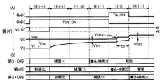
図3に示すように、単位期間H[i]は、初期化期間PRSと補償期間PCPと書込期間PWRとを含む。駆動トランジスタTDRのゲート−ソース間の電圧(すなわち保持容量C1の両端間の電圧)VGSは、初期化期間PRSにて所定の電圧に初期化され、初期化期間PRSの経過後の補償期間PCPにて駆動トランジスタTDRの閾値電圧VTHに漸近する。補償期間PCPの経過後の書込期間PWRにおいて、駆動トランジスタTDRの電圧VGSは、画素回路Uに指定された階調値Dに応じた電圧に設定される。単位期間H[i]の経過後の駆動期間PDRにおいては、駆動トランジスタTDRの電圧VGSに応じた駆動電流IDRが給電線16から駆動トランジスタTDRを経由して発光素子Eに供給される。発光素子Eは、駆動電流IDRに応じた輝度で発光する。以下では、初期化期間PRSと補償期間PCPと書込期間PWRと駆動期間PDRとに区分して、画素回路Uの具体的な動作を説明する。
As shown in FIG. 3, the unit period H [i] includes an initialization period PRS, a compensation period PCP, and a writing period PWR. The voltage VGS between the gate and the source of the driving transistor TDR (that is, the voltage across the holding capacitor C1) VGS is initialized to a predetermined voltage in the initialization period PRS, and in the compensation period PCP after the initialization period PRS has elapsed. Asymptotically approaches the threshold voltage VTH of the driving transistor TDR. In the writing period PWR after the compensation period PCP has elapsed, the voltage VGS of the driving transistor TDR is set to a voltage corresponding to the gradation value D specified in the pixel circuit U. In the driving period PDR after the elapse of the unit period H [i], the driving current IDR corresponding to the voltage VGS of the driving transistor TDR is supplied from the
[1]初期化期間PRS(図4)
図3および図4に示すように、初期化期間PRSにおいては、信号線駆動回路34が信号S[j]を基準電位VREFに設定し、電位制御回路36が電位VEL[i]を電位V2に設定する。選択スイッチTSLはオン状態であるから、駆動トランジスタTDRのゲートの電位VGは、信号線14と選択スイッチTSLとを介して信号S[j]の基準電位VREFに設定される。また、駆動トランジスタTDRのソースの電位VSは電位V2に設定される。すなわち、駆動トランジスタTDRの電圧VGS(保持容量C1の両端間の電圧)は、基準電位VREFと電位V2との差分の電圧VGS1(VGS1=VREF−V2)に初期化される。
[1] Initialization period PRS (Fig. 4)
As shown in FIGS. 3 and 4, in the initialization period PRS, the signal
基準電位VREFおよび電位V2は、以下の数式(1)のように両者の差分の電圧VGS1が駆動トランジスタTDRの閾値電圧VTHを充分に上回り、かつ、数式(2)のように発光素子Eの両端間の電圧(V2−VCT)が発光素子Eの閾値電圧VTH_OLEDを充分に下回るように設定される。したがって、初期化期間PRSにおいては、駆動トランジスタTDRがオン状態となり、発光素子Eがオフ状態(非発光状態)となる。
VGS1=VREF−V2≫VTH ……(1)
V2−VCT≪VTH_OLED……(2)
The reference potential VREF and the potential V2 are such that the difference voltage VGS1 between them is sufficiently higher than the threshold voltage VTH of the driving transistor TDR as shown in the following formula (1), and both ends of the light emitting element E as shown in the formula (2). The voltage (V2-VCT) between them is set to be sufficiently lower than the threshold voltage VTH_OLED of the light emitting element E. Therefore, in the initialization period PRS, the driving transistor TDR is turned on, and the light emitting element E is turned off (non-light emitting state).
VGS1 = VREF-V2 >> VTH (1)
V2−VCT << VTH_OLED …… (2)
[2]補償期間PCP(図5)
図3および図5に示すように、補償期間PCPが開始すると、電位制御回路36は、給電線16の電位VEL[i](駆動トランジスタTDRのドレインの電位)を電位V1に変化させる。図3に示すように、電位V1は、電位V2や基準電位VREFを充分に上回る。一方、信号線駆動回路34は、初期化期間PRSと同様に信号S[j]を基準電位VREFに維持する。選択スイッチTSLは補償期間PCPでもオン状態を維持するから、駆動トランジスタTDRのゲートの電位VGは基準電位VREFに維持される。駆動トランジスタTDRは初期化期間PRSにてオン状態に遷移しているから、以上の状態のもとでは、図5に示すように、以下の数式(3)で表現される電流Idsが駆動トランジスタTDRのドレインとソースとの間に流れる。数式(3)のμは駆動トランジスタTDRの移動度である。また、W/Lは、駆動トランジスタTDRのチャネル長Lに対するチャネル幅Wの相対比であり、Coxは、駆動トランジスタTDRのゲート絶縁膜の単位面積あたりの容量である。
Ids=1/2・μ・W/L・Cox・(VGS−VTH)2 ……(3)
[2] Compensation period PCP (Fig. 5)
As shown in FIGS. 3 and 5, when the compensation period PCP starts, the
Ids = 1/2 ・ μ ・ W / L ・ Cox ・ (VGS−VTH) 2 …… (3)
給電線16から駆動トランジスタTDRを経由して電流Idsが流れることで保持容量C1および容量C2に電荷が充電される。したがって、図3に示すように駆動トランジスタTDRのソースの電位VSは徐々に上昇する。駆動トランジスタTDRのゲートの電位VGは基準電位VREFに固定されるから、駆動トランジスタTDRのゲート−ソース間の電圧VGSはソースの電位VSの上昇とともに低下する。数式(3)から理解されるように電圧VGSが低下して閾値電圧VTHに接近するほど電流Idsは減少する。したがって、補償期間PCPにおいては、駆動トランジスタTDRの電圧VGSを、初期化期間PRSにて設定された電圧VGS1(VGS1=VREF−V2)から閾値電圧VTHに漸近させる動作(以下「第1補償動作」という)が実行される。補償期間PCPの時間長は、駆動トランジスタTDRの電圧VGSが補償期間PCPの終点にて閾値電圧VTHに充分に接近する(理想的には合致する)ように設定される。したがって、駆動トランジスタTDRは、補償期間PCPの終点にて殆どオフ状態となる。
When the current Ids flows from the
[3]書込期間PWR(図6)
図3に示すように、書込期間PWRは待機期間PWR1と動作期間PWR2とに区分される。待機期間PWR1は、書込期間PWRの始点から時間長taが経過するまでの期間であり、動作期間PWR2は、書込期間PWRの残余の期間(待機期間PWR1の終点から書込期間PWRの終点までの時間長tbの期間)である。動作期間PWR2の時間長tbは、画素回路Uに指定された階調値Dに応じて可変に設定される。すなわち、図3に示すように、階調値Dが高階調(高輝度)を指定する場合の時間長tbは、階調値Dが低階調(低輝度)を指定する場合の時間長tbと比較して短い。書込期間PWRの時間長は固定値であるから、待機期間PWR1の時間長taは時間長tb(階調値D)に応じて変化する。なお、動作期間PWR2の時間長tbの設定については後述する。
[3] Write period PWR (FIG. 6)
As shown in FIG. 3, the writing period PWR is divided into a standby period PWR1 and an operation period PWR2. The waiting period PWR1 is a period from the start point of the writing period PWR until the time length ta elapses, and the operation period PWR2 is the remaining period of the writing period PWR (from the end point of the waiting period PWR1 to the end point of the writing period PWR). Period of time length tb). The time length tb of the operation period PWR2 is variably set according to the gradation value D specified for the pixel circuit U. That is, as shown in FIG. 3, the time length tb when the gradation value D designates a high gradation (high luminance) is the time length tb when the gradation value D designates a low gradation (low luminance). Short compared to. Since the time length of the writing period PWR is a fixed value, the time length ta of the standby period PWR1 changes according to the time length tb (tone value D). The setting of the time length tb of the operation period PWR2 will be described later.
図3に示すように、待機期間PWR1では補償期間PCPの状態が維持される。すなわち、駆動トランジスタTDRのゲートに対する基準電位VREFの供給が継続されたまま、駆動トランジスタTDRは、第1補償動作で電圧VGSが閾値電圧VTHに設定された結果としてオフ状態を維持する。 As shown in FIG. 3, in the standby period PWR1, the state of the compensation period PCP is maintained. That is, while the supply of the reference potential VREF to the gate of the drive transistor TDR is continued, the drive transistor TDR maintains the off state as a result of the voltage VGS being set to the threshold voltage VTH in the first compensation operation.
図3および図6に示すように、時間長taが経過して動作期間PWR2の始点が到来すると、信号線駆動回路34は、信号S[j]を階調電位VDATAに変化させる。階調電位VDATAは、画素回路U(発光素子E)に指定された階調値Dに応じて可変に設定される。選択スイッチTSLは動作期間PWR2でもオン状態を維持するから、駆動トランジスタTDRのゲートの電位VGは、待機期間PWR1における基準電位VREFから階調電位VDATAに変化する。駆動トランジスタTDRのゲートとソースとの間には保持容量C1が介在するから、図3に示すように、駆動トランジスタTDRのソースの電位VSはゲートの電位VGに連動して変化(上昇)する。動作期間PWR2の開始の直後における電位VSの変化量は、電位VGの変化量ΔVDATA(ΔVDATA=VDATA−VREF)を保持容量C1と容量C2との容量比に応じて分割した電圧(ΔVDATA・cp1/(cp1+cp2))に相当する。したがって、動作期間PWR2の開始の直後における駆動トランジスタTDRのゲート−ソース間(保持容量C1の両端間)の電圧VGS2は、図6に示すように以下の数式(4)で表現される。数式(4)における電圧VINは、駆動トランジスタTDRのゲートに階調電位VDATAを供給したときのゲート−ソース間の電圧VGSの変化量(ΔVDATA・cp2/(cp1+cp2))に相当する。
VGS2=VTH+ΔVDATA・cp2/(cp1+cp2)
=VIN+VTH ……(4)
As shown in FIGS. 3 and 6, when the time length ta elapses and the start point of the operation period PWR2 arrives, the signal
VGS2 = VTH + ΔVDATA · cp2 / (cp1 + cp2)
= VIN + VTH (4)
以上のように電圧VGS2が階調電位VDATA(さらに詳細には階調電位VDATAと基準電位VREFとの差分)に応じて閾値電圧VTHを上回る電圧に設定されることで、駆動トランジスタTDRはオン状態に変化する。したがって、駆動トランジスタTDRのドレイン−ソース間には数式(3)の電流Idsが流れる。 As described above, the voltage VGS2 is set to a voltage exceeding the threshold voltage VTH according to the gradation potential VDATA (more specifically, the difference between the gradation potential VDATA and the reference potential VREF), so that the driving transistor TDR is turned on. To change. Therefore, the current Ids of Expression (3) flows between the drain and source of the driving transistor TDR.
電流Idsによる保持容量C1や容量C2の充電とともに駆動トランジスタTDRのソースの電位VS(容量C2の両端間の電圧)は徐々に上昇する。一方、駆動トランジスタTDRのゲートの電位VGは動作期間PWR2にて階調電位VDATAに維持される。したがって、駆動トランジスタTDRのゲート−ソース間の電圧VGSは、動作期間PWR2の開始の直後の電圧VGS2から電位VSの上昇とともに低下する。電圧VGSが閾値電圧VTHに接近するほど電流Idsは減少するから、補償期間PCPと同様に、書込期間PWRの動作期間PWR2においては、駆動トランジスタTDRの電圧VGSを、階調電位VDATAの供給で設定された電圧VGS2から閾値電圧VTHに漸近させる動作(以下「第2補償動作」という)が実行される。したがって、動作期間PWR2の終点(書込期間PWRの終点)においては、図3に示すように、駆動トランジスタTDRのゲート−ソース間の電圧VGSが、式(4)の電圧VGS2よりも電圧ΔVだけ低い数式(5)の電圧VGS3に設定される。電圧ΔVは、第2補償動作による駆動トランジスタTDRのソースの電位VSの変化量に相当する。
VGS3=VGS2−ΔV
=VIN+VTH−ΔV ……(5)
電圧VGS3は、階調電位VDATAおよび時間長tbに応じて変化する。したがって、動作期間PWR2の時間長tbを階調値Dに応じて制御する動作は、動作期間PWR2の終点における電圧VGS3を階調値Dに応じて可変に制御する動作としても把握される。
As the holding capacitor C1 and the capacitor C2 are charged by the current Ids, the source potential VS (voltage across the capacitor C2) of the drive transistor TDR gradually increases. On the other hand, the gate potential VG of the driving transistor TDR is maintained at the gradation potential VDATA during the operation period PWR2. Accordingly, the gate-source voltage VGS of the drive transistor TDR decreases from the voltage VGS2 immediately after the start of the operation period PWR2 as the potential VS increases. Since the current Ids decreases as the voltage VGS approaches the threshold voltage VTH, in the operation period PWR2 of the writing period PWR, the voltage VGS of the driving transistor TDR is supplied by the supply of the gradation potential VDATA, as in the compensation period PCP. An operation (hereinafter referred to as “second compensation operation”) for gradually approaching the set voltage VGS2 to the threshold voltage VTH is performed. Therefore, at the end point of the operation period PWR2 (end point of the write period PWR), as shown in FIG. 3, the voltage VGS between the gate and the source of the drive transistor TDR is a voltage ΔV higher than the voltage VGS2 of the equation (4). The voltage VGS3 of the low equation (5) is set. The voltage ΔV corresponds to the amount of change in the source potential VS of the drive transistor TDR due to the second compensation operation.
VGS3 = VGS2-ΔV
= VIN + VTH-ΔV (5)
The voltage VGS3 changes according to the gradation potential VDATA and the time length tb. Therefore, the operation of controlling the time length tb of the operation period PWR2 according to the gradation value D can be understood as an operation of variably controlling the voltage VGS3 at the end point of the operation period PWR2 according to the gradation value D.
動作期間PWR2の始点から駆動トランジスタTDRがオン状態に変化するまでの時間長は充分に短いから、動作期間PWR2の時間長tbは第2補償動作が実行される時間長に相当する。時間長tbは、動作期間PWR2の終点における駆動トランジスタTDRのゲート−ソース間の電圧VGS3が、閾値電圧VTHと同等の電圧(階調値Dが最低階調を指定する場合)または閾値電圧VTHを上回る電圧となる範囲内で設定される。すなわち、階調値Dが最低階調以外の階調を指定する場合には動作期間PWR2の終点にて駆動トランジスタTDRはオン状態を維持する。 Since the time length from the start point of the operation period PWR2 until the drive transistor TDR changes to the ON state is sufficiently short, the time length tb of the operation period PWR2 corresponds to the time length during which the second compensation operation is performed. The time length tb is a voltage VGS3 between the gate and source of the driving transistor TDR at the end of the operation period PWR2 equal to the threshold voltage VTH (when the gradation value D specifies the lowest gradation) or the threshold voltage VTH. It is set within the range where the voltage is higher. That is, when the gradation value D designates a gradation other than the lowest gradation, the drive transistor TDR is kept on at the end point of the operation period PWR2.
[4]駆動期間PDR(図7)
図3および図7に示すように、駆動期間PDRが開始すると、走査線駆動回路32は走査信号GA[i]を非アクティブレベル(ローレベル)に変化させる。したがって、第i行目の各画素回路Uの選択スイッチTSLはオフ状態に変化し、駆動トランジスタTDRのゲートは電気的なフローティング状態となる(すなわち、駆動トランジスタTDRのゲートに対する電位の供給が停止する)。一方、書込期間PWRにてオン状態に設定された駆動トランジスタTDRのドレイン−ソース間に数式(3)の電流Idsが流れることで容量C2が充電される。したがって、図3に示すように、駆動トランジスタTDRの電圧VGSが書込期間PWRの終点での電圧VGS3に維持されたまま、容量C2の両端間の電圧(駆動トランジスタTDRのソースの電位VS)が徐々に増加する。そして、容量C2の両端間の電圧が発光素子Eの閾値電圧VTH_OLEDに到達した時点で電流Idsが駆動電流IDRとして発光素子Eを流れる。したがって、駆動電流IDRは以下の数式(6)で表現される。
IDR=1/2・μ・W/L・Cox・(VGS3−VTH)2
=1/2・μ・W/L・Cox・{(VIN+VTH−ΔV)−VTH}2
=K・(VIN−ΔV)2 ……(6)
K=1/2・μ・W/L・Cox
以上のように駆動電流IDRは、階調電位VDATAを反映した電圧VGS3に応じた電流量に制御されるから、発光素子Eは階調電位VDATA(すなわち階調値D)に応じた輝度で発光する。発光素子Eの発光は、走査信号GA[i]が次にアクティブレベルとなる単位期間H[i]の開始まで継続される。
[4] Driving period PDR (FIG. 7)
As shown in FIGS. 3 and 7, when the driving period PDR starts, the scanning
IDR = 1/2 ・ μ ・ W / L ・ Cox ・ (VGS3−VTH) 2
= 1/2 · μ · W / L · Cox · {(VIN + VTH−ΔV) −VTH} 2
= K ・ (VIN-ΔV) 2 …… (6)
K = 1/2 ・ μ ・ W / L ・ Cox
As described above, since the drive current IDR is controlled by the amount of current corresponding to the voltage VGS3 reflecting the gradation potential VDATA, the light emitting element E emits light with luminance corresponding to the gradation potential VDATA (that is, the gradation value D). To do. The light emission of the light emitting element E is continued until the start of the unit period H [i] when the scanning signal GA [i] becomes the active level next time.
数式(5)の電圧VGS3は、補償期間PCPで設定された閾値電圧VTHを階調電位VDATAに応じて変化させた電圧であるから、数式(6)に示すように駆動電流IDRは閾値電圧VTHに依存しない。したがって、各画素回路Uの駆動トランジスタTDRの閾値電圧VTHに誤差がある場合でも、駆動電流IDRは階調電位VDATAに対応した目標値に設定される。すなわち、各画素回路Uの駆動トランジスタTDRの閾値電圧VTHに起因した駆動電流IDRの誤差は、補償期間PCPにおける第1補償動作で補償される。 Since the voltage VGS3 in the equation (5) is a voltage obtained by changing the threshold voltage VTH set in the compensation period PCP according to the gradation potential VDATA, the drive current IDR is expressed by the threshold voltage VTH as shown in the equation (6). Does not depend on. Therefore, even when there is an error in the threshold voltage VTH of the drive transistor TDR of each pixel circuit U, the drive current IDR is set to a target value corresponding to the gradation potential VDATA. That is, the error of the drive current IDR caused by the threshold voltage VTH of the drive transistor TDR of each pixel circuit U is compensated by the first compensation operation in the compensation period PCP.
また、数式(6)の電圧ΔV(第2補償動作による駆動トランジスタTDRのゲート−ソース間の電圧VGSの変化量)は駆動トランジスタTDRの移動度μに依存する。さらに詳述すると、駆動トランジスタTDRの移動度μが大きいほど電圧ΔVは増加する。以上のように駆動トランジスタTDRの移動度μが第2補償動作で駆動電流IDRに反映されるから、駆動トランジスタTDRの移動度μに起因した駆動電流IDRの誤差を、書込期間PWR(動作期間PWR2)における第2補償動作で補償することが可能である。 In addition, the voltage ΔV (the amount of change in the voltage VGS between the gate and the source of the driving transistor TDR due to the second compensation operation) in Expression (6) depends on the mobility μ of the driving transistor TDR. More specifically, the voltage ΔV increases as the mobility μ of the drive transistor TDR increases. As described above, the mobility μ of the drive transistor TDR is reflected in the drive current IDR in the second compensation operation. Therefore, the error of the drive current IDR caused by the mobility μ of the drive transistor TDR is represented by the writing period PWR (operation period It is possible to compensate by the second compensation operation in PWR2).
しかし、第2補償動作の時間長tbを、階調値Dに依存しない所定値に固定した構成(以下「対比例」という)のもとでは、以下に説明するように、駆動トランジスタTDRの移動度μの誤差を有効に補償できるのが、特定の階調値D(階調電位VDATA)を指定した場合に制限されるという問題がある。 However, under the configuration in which the time length tb of the second compensation operation is fixed to a predetermined value that does not depend on the gradation value D (hereinafter referred to as “proportional”), as described below, the movement of the drive transistor TDR There is a problem that the error of the degree μ can be effectively compensated only when a specific gradation value D (gradation potential VDATA) is designated.
図8は、対比例における階調電位VDATAと駆動電流IDRの電流量の誤差との相関を示すグラフである。図8の横軸は、基準電位VREFを基準値(0.0)とした階調電位VDATAの電圧値を意味し、図8の縦軸は、所定の階調値Dが指定された場合の駆動電流IDRの電流量の最大値と最小値との相対比(最大誤差比)を意味する。図8から理解されるように、第2補償動作の時間長tbを固定値とした場合、階調電位VDATAが所定値VD0に設定された場合には駆動電流IDRの誤差は確かに低減されるが、階調電位VDATAが所定値VD0から離れるほど駆動電流IDRの誤差が増大する。すなわち、対比例においては、駆動トランジスタTDRの移動度μに起因した駆動電流IDRの誤差を階調電位VDATAの広い範囲にわたって抑制することが困難であるという問題がある。 FIG. 8 is a graph showing the correlation between the gradation potential VDATA and the error in the current amount of the driving current IDR in the comparative example. The horizontal axis in FIG. 8 represents the voltage value of the gradation potential VDATA with the reference potential VREF as the reference value (0.0), and the vertical axis in FIG. 8 represents the drive current when the predetermined gradation value D is designated. It means the relative ratio (maximum error ratio) between the maximum value and the minimum value of the current amount of IDR. As understood from FIG. 8, when the time length tb of the second compensation operation is set to a fixed value, the error of the drive current IDR is surely reduced when the gradation potential VDATA is set to the predetermined value VD0. However, the error of the drive current IDR increases as the gradation potential VDATA is separated from the predetermined value VD0. That is, in contrast, there is a problem that it is difficult to suppress the error of the drive current IDR caused by the mobility μ of the drive transistor TDR over a wide range of the gradation potential VDATA.
図9は、動作期間PWR2の時間長tbと駆動電流IDRの誤差(最大誤差比)との関係を、階調電位VDATAを変化させた複数の場合(VD1<VD2<VD3<VD4<VD5)について計算したグラフである。駆動電流IDRの誤差が最小となる時間長tbは階調電位VDATAに応じて相違するという傾向が図9から見出される。すなわち、階調電位VDATAが高いほど、駆動電流IDRの誤差が最小となる時間長tbは短くなる。以上の知見から、本形態においては、動作期間PWR2の時間長tbを階調値D(階調電位VDATA)に応じて可変に設定することで、階調電位VDATAの高低に拘わらず駆動電流IDRの誤差を抑制する。例えば、階調電位VDATAが図9の電位VD1に設定される場合には時間長tbが所定値T1に設定され、階調電位VDATAが電位VD1よりも高い電位VD2に設定される場合には時間長tbが所定値T2(T2<T1)に設定されるといった具合である。 FIG. 9 shows the relationship between the time length tb of the operation period PWR2 and the error (maximum error ratio) of the drive current IDR for a plurality of cases where the gradation potential VDATA is changed (VD1 <VD2 <VD3 <VD4 <VD5). It is the calculated graph. It can be seen from FIG. 9 that the time length tb at which the error of the drive current IDR is minimized differs depending on the gradation potential VDATA. That is, the higher the gradation potential VDATA, the shorter the time length tb at which the drive current IDR error is minimized. From the above knowledge, in this embodiment, the drive current IDR is set regardless of the level of the gradation potential VDATA by variably setting the time length tb of the operation period PWR2 in accordance with the gradation value D (gradation potential VDATA). Suppress errors. For example, when the gradation potential VDATA is set to the potential VD1 in FIG. 9, the time length tb is set to the predetermined value T1, and when the gradation potential VDATA is set to the potential VD2 higher than the potential VD1, the time is set. The length tb is set to a predetermined value T2 (T2 <T1).
次に、動作期間PWR2内の第2補償動作について詳細に検討する。第2補償動作の実行中に駆動トランジスタTDRのドレイン−ソース間に流れる電流Idsと、電流Idsで充電される容量(保持容量C1および容量C2)の容量値との間には、以下の数式(7)の関係が成立する。数式(7)におけるCは、保持容量C1と容量C2との容量値の合計(C=cp1+cp2)である。
Ids=dQ/dt=C・(dVS/dt) ……(7)
また、駆動トランジスタTDRのソースの電位VSの時間的な変化が電圧ΔVの時間的な変化と同等であること(dVS/dt=dΔV/dt)を考慮すると、数式(6)と数式(7)とから以下の数式(8)が導出される。なお、数式(8)における電圧ΔV(t)は、第2補償動作の開始(動作期間PWR2の始点)から経過した時間tに応じて数式(6)の電圧ΔVが変化することを意味する。
C(dΔV/dt)=K(VIN−ΔV(t))2 ……(8)
Next, the second compensation operation within the operation period PWR2 will be examined in detail. Between the current Ids flowing between the drain and source of the drive transistor TDR during execution of the second compensation operation and the capacitance value of the capacitors (holding capacitor C1 and capacitor C2) charged by the current Ids, the following formula ( The relationship of 7) is established. C in Expression (7) is the sum of the capacitance values of the storage capacitor C1 and the capacitor C2 (C = cp1 + cp2).
Ids = dQ / dt = C · (dVS / dt) (7)
Considering that the temporal change of the source potential VS of the driving transistor TDR is equivalent to the temporal change of the voltage ΔV (dVS / dt = dΔV / dt), the equations (6) and (7) From the above, the following formula (8) is derived. The voltage ΔV (t) in the equation (8) means that the voltage ΔV in the equation (6) changes according to the time t that has elapsed since the start of the second compensation operation (the start point of the operation period PWR2).
C (dΔV / dt) = K (VIN−ΔV (t)) 2 (8)
動作期間PWR2の始点(t=0)において電圧ΔV(t)(ΔV(0))がゼロであるという条件のもとで数式(8)を積分すると、動作期間PWR2の終点(t=tb)における駆動トランジスタTDRのドレイン−ソース間の電流Ids(tb)を表す以下の数式(9)が導出される。

When Equation (8) is integrated under the condition that the voltage ΔV (t) (ΔV (0)) is zero at the start point (t = 0) of the operation period PWR2, the end point (t = tb) of the operation period PWR2 The following formula (9) representing the drain-source current Ids (tb) of the driving transistor TDR in FIG.
数式(9)の係数Kは、数式(6)に併記したように駆動トランジスタTDRの移動度μを含むから、移動度μの誤差の程度を表す指標に相当する。駆動期間PDRにて発光素子Eに供給される駆動電流IDRは数式(9)の電流Ids(tb)に依存するから、駆動電流IDRの誤差を最小化するためには、係数K(移動度μ)の変動に対する電流Ids(tb)の誤差を最小化する必要がある。そして、係数Kの変動に対して電流Ids(tb)の誤差が最小となるのは、数式(9)を係数Kで微分した結果がゼロとなる場合である。以上の条件から数式(10)が導出される。
Since the coefficient K in Equation (9) includes the mobility μ of the drive transistor TDR as described in Equation (6), it corresponds to an index representing the degree of error in the mobility μ. Since the drive current IDR supplied to the light emitting element E in the drive period PDR depends on the current Ids (tb) of the equation (9), in order to minimize the error of the drive current IDR, the coefficient K (mobility μ ) To minimize the error in the current Ids (tb). The error of the current Ids (tb) is minimized with respect to the variation of the coefficient K when the result obtained by differentiating the equation (9) by the coefficient K is zero. Equation (10) is derived from the above conditions.
したがって、第2補償動作による駆動電流IDRの補償の効果が最大となる条件は以下の数式(11)で表現される。
C=KVINtb ……(11)
数式(11)の電圧VINは階調電位VDATAに応じて設定されるから、階調電位VDATAと動作期間PWR2の時間長tbとについて、図9を参照して説明したのと同様の条件(階調電位VDATAが高いほど時間長tbを短くする)が数式(11)からも確認される。さらに詳述すると、電圧VINと動作期間PWR2の時間長tbとの乗算値(あるいは階調電位VDATAと時間長tbとの乗算値)が所定値となる場合に、第2補償動作による駆動電流IDRの補償の効果が最大となる。
Accordingly, the condition that maximizes the effect of the compensation of the drive current IDR by the second compensation operation is expressed by the following formula (11).
C = KVINtb (11)
Since the voltage VIN in the equation (11) is set according to the gradation potential VDATA, the same conditions (steps) as those described with reference to FIG. 9 are used for the gradation potential VDATA and the time length tb of the operation period PWR2. The time length tb is shortened as the adjustment potential VDATA is higher). More specifically, when the multiplication value of the voltage VIN and the time length tb of the operation period PWR2 (or the multiplication value of the gradation potential VDATA and the time length tb) becomes a predetermined value, the drive current IDR by the second compensation operation The effect of compensation is maximized.
図9および数式(11)を参照して説明した以上の知見から、本形態においては、階調電位VDATAと時間長tbとの関係を図10のように設定する。図10に示すように、階調電位VDATAが高い(階調電位VDATAの供給による駆動トランジスタTDRのゲート−ソース間の電圧VGSの変化量VINが高い)ほど、動作期間PWR2の時間長tbは短い時間に設定される。さらに詳述すると、数式(11)から理解されるように、階調電位VDATA(電圧VIN)と時間長tbとの乗算値が所定値となる(時間長tbが階調電位VDATAに対して反比例する)ように時間長tbが設定される。例えば、複数種の階調電位VDATAの各々に対応する時間長tbは、当該階調電位VDATAに応じて設定される駆動電流IDRの誤差が例えば1%以下に低減(理想的には最小化)されるように設定される。 From the above knowledge described with reference to FIG. 9 and Equation (11), in this embodiment, the relationship between the gradation potential VDATA and the time length tb is set as shown in FIG. As shown in FIG. 10, the time length tb of the operation period PWR2 is shorter as the gradation potential VDATA is higher (the amount of change VIN of the gate-source voltage VGS of the driving transistor TDR due to the supply of the gradation potential VDATA is higher). Set to time. More specifically, as can be understood from Equation (11), the multiplication value of the gradation potential VDATA (voltage VIN) and the time length tb becomes a predetermined value (the time length tb is inversely proportional to the gradation potential VDATA. Time length tb is set. For example, the time length tb corresponding to each of the plurality of types of gradation potential VDATA reduces the error of the drive current IDR set according to the gradation potential VDATA to, for example, 1% or less (ideally minimized). To be set.
ただし、駆動電流IDRの誤差を最小化するための時間長tbは階調電位VDATAが低いほど長いから、階調電位VDATAが充分に低い場合(例えば最低階調が指定された場合)にも駆動電流IDRの誤差を厳密に最小化しようとすれば、時間長tbを過度に長い時間に設定する必要がある。そこで、本形態の信号線駆動回路34は、図10に示すように、所定値を下回る階調値Dが指定された場合(階調電位VDATAが図10の電位VD_thを下回る場合)、動作期間PWR2の時間長tbを、階調値Dに依存しない所定値tmaxに設定(クリップ)する。最大値tmaxは、駆動トランジスタTDRの電圧VGSが第2補償動作で閾値電圧VTHまで低下するのに必要な時間長よりも短い時間に制限される。以上の構成によれば、書込期間PWR(さらには単位期間H)を短くすることが可能である。
However, since the time length tb for minimizing the error of the driving current IDR is longer as the gradation potential VDATA is lower, the driving is performed even when the gradation potential VDATA is sufficiently low (for example, when the lowest gradation is designated). In order to minimize the error of the current IDR, it is necessary to set the time length tb to an excessively long time. Therefore, as shown in FIG. 10, the signal
図3を参照して説明したように、書込期間PWR内の第2補償動作は、信号S[j](駆動トランジスタTDRのゲートの電位VG)が基準電位VREFから階調電位VDATAに変化することで開始する。そこで、信号線駆動回路34の各単位回路40は、信号S[j]を基準電位VREFから階調電位VDATAに変化させる時点を階調値Dに応じて調整することで、動作期間PWR2の時間長tb(待機期間PWR1の時間長ta)を可変に制御する。
As described with reference to FIG. 3, in the second compensation operation within the writing period PWR, the signal S [j] (the gate potential VG of the driving transistor TDR) changes from the reference potential VREF to the gradation potential VDATA. Start with that. Therefore, each
図11は、信号線駆動回路34の単位回路40のブロック図である。図11においては信号S[j]を生成および出力する1個の単位回路40のみが代表的に図示されている。図11に示すように、単位回路40は、電位生成部42と電位選択部44と時間調整部46とを含んで構成される。第j番目の画素回路Uの階調値Dが電位生成部42と時間調整部46とに供給される。
FIG. 11 is a block diagram of the
電位生成部42は、階調値Dに応じた階調電位VDATAを生成する。例えば、電圧出力型のD/A変換器が電位生成部42として利用される。電位選択部44には、電源回路(図示略)が生成した基準電位VREFと電位生成部42が生成した階調電位VDATAとが供給される。電位選択部44は、基準電位VREFと階調電位VDATAとの何れかを選択的に信号S[j]として信号線14に出力する。さらに詳述すると、電位選択部44は、初期化期間PRSおよび補償期間PCPと書込期間PWRの待機期間PWR1とにおいて基準電位VREFを出力し、書込期間PWRの動作期間PWR2にて階調電位VDATAを出力する。
The
時間調整部46は、電位選択部44が信号S[j]の電位を基準電位VREFから階調電位VDATAに変更する時点(すなわち待機期間PWR1と動作期間PWR2との境界)を階調値Dに応じて可変に制御する。例えば、書込期間PWRの始点にて計数を開始するとともに計数値が階調値Dに応じた数値に到達した時点(計数の開始から時間長taが経過した時点)で電位の切替(VREF→VDATA)の指示を電位選択部44に出力するカウンタ回路が時間調整部46として利用される。時間調整部46が時間長tbを最大値tmaxに制限する点は前述の通りである。
The
図12は、本形態における階調電位VDATAと駆動電流IDRの誤差との関係(実線)を示すグラフである。図12においては、対比例における階調電位VDATAと駆動電流IDRの誤差との相関(図8)が破線で併記されている。図12に示すように、本形態によれば、第2補償動作の時間長tbが階調値Dによらず固定された対比例(例えば特許文献1)と比較して、階調電位VDATAの広い範囲にわたって駆動電流IDRの誤差が1%以下に抑制されるという利点がある。 FIG. 12 is a graph showing a relationship (solid line) between the gradation potential VDATA and the error of the drive current IDR in this embodiment. In FIG. 12, the correlation (FIG. 8) between the gray scale potential VDATA and the error of the drive current IDR in the proportional proportion is also shown by a broken line. As shown in FIG. 12, according to the present embodiment, the time length tb of the second compensation operation is compared with the fixed proportionality (for example, Patent Document 1) regardless of the gradation value D. There is an advantage that the error of the drive current IDR is suppressed to 1% or less over a wide range.
なお、図12において階調電位VDATAの低位側の領域で駆動電流IDRの誤差が僅かに増加しているのは、時間長tbの上限を最大値tmaxに制限した影響と考えられる。もっとも、駆動電流IDRの誤差が低位側で増加しているとは言っても、対比例と比較して駆動電流IDRの誤差が大幅に改善されることは図12から明白である。 In FIG. 12, the slight increase in the error of the drive current IDR in the lower region of the gradation potential VDATA is considered to be the effect of limiting the upper limit of the time length tb to the maximum value tmax. However, it is clear from FIG. 12 that the error of the drive current IDR is greatly improved compared to the proportionality even though the error of the drive current IDR increases on the lower side.
駆動電流IDRの誤差の主要因は駆動トランジスタTDRの閾値電圧VTHおよび移動度μの誤差である。閾値電圧VTHの誤差は、駆動トランジスタTDRの電圧VGSを閾値電圧VTHに設定する第1補償動作で補償されるから、第2補償動作は、駆動トランジスタTDRの移動度μの誤差を補償するための動作として把握される。すなわち、本形態においては、駆動トランジスタTDRの移動度μの誤差が階調電位VDATAの広い範囲にわたって補償されるように、動作期間PWR2の時間長tbが階調値Dに応じて可変に制御される。 The main cause of the error in the drive current IDR is an error in the threshold voltage VTH and mobility μ of the drive transistor TDR. Since the error of the threshold voltage VTH is compensated by the first compensation operation for setting the voltage VGS of the drive transistor TDR to the threshold voltage VTH, the second compensation operation is for compensating the error of the mobility μ of the drive transistor TDR. It is grasped as an operation. That is, in this embodiment, the time length tb of the operation period PWR2 is variably controlled according to the gradation value D so that the error of the mobility μ of the driving transistor TDR is compensated over a wide range of the gradation potential VDATA. The
<B:第2実施形態>
次に、本発明の第2実施形態について説明する。なお、以下の各形態において作用や機能が第1実施形態と同様である要素については、以上と同じ符号を付して各々の詳細な説明を適宜に省略する。
<B: Second Embodiment>
Next, a second embodiment of the present invention will be described. In addition, about the element which an effect | action and function are the same as that of 1st Embodiment in each following form, the same code | symbol as the above is attached | subjected and each detailed description is abbreviate | omitted suitably.
第1実施形態においては、単位期間H[i]内の補償期間PCPにて第i行の各画素回路Uについて第1補償動作を実行した。しかし、駆動トランジスタTDRのゲート−ソース間の電圧VGSが閾値電圧VTHに到達するまでに相当の時間が掛かる場合、単位期間H[i]を長時間に設定する必要がある。そして、単位期間H[i]が長期化するほど画素回路Uの高精細化(行数の増加)が制約されるという問題がある。そこで、本形態においては、複数の単位期間Hにわたって第1補償動作を実行することで、単位期間Hの時間長を短縮しながら駆動トランジスタTDRの電圧VGSを確実に閾値電圧VTHに設定する。 In the first embodiment, the first compensation operation is performed for each pixel circuit U in the i-th row in the compensation period PCP within the unit period H [i]. However, if it takes a considerable time for the gate-source voltage VGS of the drive transistor TDR to reach the threshold voltage VTH, the unit period H [i] needs to be set to a long time. Then, there is a problem that the higher the unit circuit H [i], the more restricted the pixel circuit U is to have higher definition (increase in the number of rows). Therefore, in this embodiment, by executing the first compensation operation over a plurality of unit periods H, the voltage VGS of the drive transistor TDR is reliably set to the threshold voltage VTH while shortening the time length of the unit period H.
図13は、第2実施形態における画素回路Uの回路図である。図13に示すように、本形態の画素回路Uは、第1実施形態の画素回路Uに制御スイッチTCR1を追加した構成である。制御スイッチTCR1は、駆動トランジスタTDRのドレイン−ソース間の電流Ids(駆動電流IDR)の経路上に配置される。例えば、図13に示すように、駆動トランジスタTDRのドレインと給電線16との間に介在するNチャネル型のトランジスタが制御スイッチTCR1として好適である。
FIG. 13 is a circuit diagram of the pixel circuit U in the second embodiment. As shown in FIG. 13, the pixel circuit U of this embodiment has a configuration in which a control switch TCR1 is added to the pixel circuit U of the first embodiment. The control switch TCR1 is disposed on the path of the current Ids (drive current IDR) between the drain and source of the drive transistor TDR. For example, as shown in FIG. 13, an N-channel transistor interposed between the drain of the drive transistor TDR and the
素子部10内には、走査線12とともにX方向に延在するm本の制御線52が形成される。図13に示すように、第i行目の各画素回路Uにおける制御スイッチTCR1のゲートは第i行目の制御線52に接続される。各制御線52には駆動回路30(例えば走査線駆動回路32)から制御信号GB(GB[1]〜GB[m])が供給される。制御スイッチTCR1がオン状態に遷移すると電流Idsの経路が確立し、制御スイッチTCR1がオフ状態に遷移すると電流Idsの経路が遮断される。
In the
第1補償動作および第2補償動作のためには駆動トランジスタTDRに電流Idsを流す必要があるから、第1補償動作や第2補償動作の実行時には制御スイッチTCR1がオン状態に設定される。また、駆動トランジスタTDRのゲート−ソース間の電圧VGSを数式(1)の電圧VGS1に初期化する動作(以下「初期化動作」という)時には駆動トランジスタTDRのソースの電位VSが給電線16の電位V2(電位VEL[i])に設定されるから、制御スイッチTCR1は初期化動作時にもオン状態に設定される。
Since the current Ids needs to flow through the drive transistor TDR for the first compensation operation and the second compensation operation, the control switch TCR1 is set to the on state when the first compensation operation or the second compensation operation is performed. In the operation of initializing the voltage VGS between the gate and source of the drive transistor TDR to the voltage VGS1 of the equation (1) (hereinafter referred to as “initialization operation”), the source potential VS of the drive transistor TDR is the potential of the
図14は、画素回路Uを駆動する方法を説明するためのタイミングチャートである。図14の部分(A)に示すように、複数の単位期間H(……,H[i-3],H[i-2],H[i-1],H[i],H[i+1],……)の各々は期間h1と期間h2とに区分される。期間h1は単位期間Hの前半の期間であり、期間h2は単位期間Hの後半の期間である。駆動回路30は、画素回路Uに対する階調電位VDATAの供給と第2補償動作と(図14の部分(B)の「書込・補償[2]」)を単位期間Hの期間h2毎に行単位で順次に実行する。すなわち、単位期間H[i]の期間h2が第i行の各画素回路Uの書込期間PWRに相当する。
FIG. 14 is a timing chart for explaining a method of driving the pixel circuit U. As shown in part (A) of FIG. 14, a plurality of unit periods H (..., H [i-3], H [i-2], H [i-1], H [i], H [i +1],...) Are divided into periods h1 and h2. The period h1 is the first half of the unit period H, and the period h2 is the second half of the unit period H. The
図14の部分(A)に示すように、走査線駆動回路32は、単位期間H[i]の期間h2にて走査信号GA[i]および制御信号GB[i]をアクティブレベルに設定することで第i行の各画素回路Uにおける選択スイッチTSLおよび制御スイッチTCR1をオン状態に制御する。一方、信号線駆動回路34は、単位期間H[i]の期間h2のうち始点から時間長taが経過した時点(動作期間PWR2の始点)で信号S[j]を基準電位VREFから第i行の画素回路Uの階調電位VDATA[i]に変化させる。したがって、図14の部分(A)に示すように、第i行の各画素回路Uにおいては、単位期間H[i]の期間h2のうち階調値Dに応じた時間長tbにわたって第2補償動作が実行される。
As shown in part (A) of FIG. 14, the scanning
また、駆動回路30は、第i行の各画素回路Uの初期化動作(図14の部分(B)における「初期化」)と第1補償動作(図14の部分(B)における「補償[1]」)とを単位期間H[i]の期間h2の開始前の複数の期間h1にて実行する。まず、単位期間H[i]の3個前の単位期間H[i-3]の期間h1において、走査線駆動回路32は、走査信号GA[i]および制御信号GB[i]をアクティブレベルに設定することで第i行の各画素回路Uの選択スイッチTSLおよび制御スイッチTCR1をオン状態に設定する。また、図14の部分(A)に示すように、信号線駆動回路34は信号S[j]を基準電位VREFに設定し、電位制御回路36は電位VEL[i]を電位V2に設定する。したがって、第i行の各画素回路Uにおける駆動トランジスタTDRのゲート−ソース間の電圧VGSは、単位期間H[i-3]の期間h1を初期化期間PRSとして、数式(1)の電圧VGS1(VGS1=VREF−V2)に設定される。
Further, the
さらに、単位期間H[i]の期間h2の開始前の3個の期間h1(単位期間H[i-2]〜H[i]の各々の期間h1)においても、単位期間H[i-3]の期間h1と同様に、第i行の各画素回路Uの選択スイッチTSLおよび制御スイッチTCR1がオン状態に制御されるとともに信号S[j]が基準電位VREFに設定される。一方、電位制御回路36は、単位期間H[i-3]の期間h1の経過後に、第i行の給電線16の電位VEL[i]を電位V1に変化させる。したがって、第i行の各画素回路Uにおいては、単位期間H[i-2]〜H[i]の各々の期間h1を補償期間PCPとして第1補償動作が実行される。
Further, in the three periods h1 (each period h1 of the unit periods H [i-2] to H [i]) before the start of the period h2 of the unit period H [i], the unit period H [i-3 ], The selection switch TSL and the control switch TCR1 of each pixel circuit U in the i-th row are controlled to be in the ON state and the signal S [j] is set to the reference potential VREF. On the other hand, the
単位期間H[i-3]〜H[i]の各々の期間h2(すなわち、第i行以外の画素回路Uの階調電位VDATAが信号線14に供給されている期間)においては、選択スイッチTSLおよび制御スイッチTCR1がオフ状態に制御されるから、第i行の駆動トランジスタTDRのゲート−ソース間の電圧VGSは変化しない。すなわち、第i行の各画素回路Uにおいては、3個の単位期間H[i-2]〜H[i]の各々の期間h1にわたって間欠的に第1補償動作が実行されることで駆動トランジスタの電圧VGSが閾値電圧VTHに設定される。 In each period h2 of the unit periods H [i-3] to H [i] (that is, the period in which the gradation potential VDATA of the pixel circuit U other than the i-th row is supplied to the signal line 14), the selection switch Since TSL and the control switch TCR1 are controlled to be in the OFF state, the voltage VGS between the gate and the source of the driving transistor TDR in the i-th row does not change. That is, in each pixel circuit U in the i-th row, the first compensation operation is intermittently executed over each period h1 of the three unit periods H [i-2] to H [i], thereby driving transistors. Is set to the threshold voltage VTH.
単位期間H[i]が経過すると、走査線駆動回路32は、走査信号GA[i]を非アクティブレベルに設定することで選択スイッチTSLをオフ状態に変化させる。制御信号GB[i]は単位期間H[i]の経過後もアクティブレベルに維持される。したがって、第1実施形態と同様に、数式(6)の駆動電流IDRが給電線16から制御スイッチTCR1と駆動トランジスタTDRとを経由して発光素子Eに供給される。第i行の画素回路Uについて説明した以上の動作が各行についても同様に反復される。
When the unit period H [i] elapses, the scanning
以上の形態においては、複数の単位期間Hの期間h1にわたって第1補償動作が実行される。したがって、第1補償動作を1個の単位期間H内で実行する第1実施形態と比較すると、単位期間Hの時間長が短い場合であっても、駆動トランジスタTDRの電圧VGSが閾値電圧VTHに到達するのに充分な時間長を第1補償動作のために確保できるという利点がある。 In the above embodiment, the first compensation operation is executed over the period h1 of the plurality of unit periods H. Therefore, when compared with the first embodiment in which the first compensation operation is performed within one unit period H, the voltage VGS of the drive transistor TDR is equal to the threshold voltage VTH even when the time length of the unit period H is short. There is an advantage that a sufficient length of time can be secured for the first compensation operation.
<C:第3実施形態>
図15は、本発明の第3実施形態における画素回路Uの回路図である。図15に示すように、画素回路Uは、第1実施形態の画素回路Uに制御スイッチTCR2を追加した構成である。制御スイッチTCR2は、駆動トランジスタTDRのゲートと給電線54との間に介在して両者の電気的な接続(導通/非導通)を制御するNチャネル型のトランジスタである。給電線54には基準電位VREFが供給される。すなわち、第1実施形態や第2実施形態においては画素回路Uに対する基準電位VREFの供給に信号線14を兼用したのに対し、本形態においては信号線14とは別個の給電線54を利用して各画素回路Uに基準電位VREFを供給する。
<C: Third Embodiment>
FIG. 15 is a circuit diagram of a pixel circuit U in the third embodiment of the present invention. As shown in FIG. 15, the pixel circuit U has a configuration in which a control switch TCR2 is added to the pixel circuit U of the first embodiment. The control switch TCR2 is an N-channel transistor that is interposed between the gate of the driving transistor TDR and the
素子部10内には、走査線12とともにX方向に延在するm本の制御線56が形成される。図15に示すように、第i行目の各画素回路Uにおける制御スイッチTCR2のゲートは第i行目の制御線56に接続される。各制御線56には駆動回路30(例えば走査線駆動回路32)から制御信号GC(GC[1]〜GC[m])が供給される。
In the
図16は、画素回路Uを駆動する方法を説明するためのタイミングチャートである。図16の部分(B)に示すように、駆動回路30は、画素回路Uに対する階調電位VDATAの供給と第2補償動作とを単位期間H毎に行単位で順次に実行する。すなわち、単位期間H[i]が第i行の各画素回路Uの書込期間PWRに相当する。
FIG. 16 is a timing chart for explaining a method of driving the pixel circuit U. As shown in part (B) of FIG. 16, the
図16の部分(A)に示すように、走査線駆動回路32は、単位期間H[i]において、走査信号GA[i]をアクティブレベルに設定するとともに制御信号GC[i]を非アクティブレベルに設定する。したがって、選択スイッチTSLはオン状態となり、制御スイッチTCR2はオフ状態となる。一方、信号線駆動回路34は、単位期間H[i]の始点から時間長taが経過した時点で信号S[j]を基準電位VREFから階調電位VDATA[i]に変化させる。したがって、図16の部分(A)に示すように、第i行の各画素回路Uにおいては、単位期間H[i]内の時間長tbにわたって第2補償動作が実行される。
As shown in part (A) of FIG. 16, the scanning
また、駆動回路30は、第i行の各画素回路Uについて、単位期間H[i-4]を初期化期間PRSとして初期化動作を実行するとともに単位期間H[i-3]〜H[i-1]を補償期間PCPとして第1補償動作を実行する。まず、図16の部分(A)に示すように、単位期間H[i-4]において、走査線駆動回路32は、走査信号GA[i]を非アクティブレベルに設定することで選択スイッチTSLをオフ状態に制御するとともに、制御信号GC[i]をアクティブレベルに設定することで制御スイッチTCR2をオン状態に制御する。したがって、駆動トランジスタTDRのゲートには、給電線54から制御スイッチTCR2を介して基準電位VREFが供給される。一方、電位制御回路36は、単位期間H[i-4]にて電位VEL[i]を電位V2に設定する。したがって、単位期間H[i-4]においては、第1実施形態や第2実施形態と同様に、駆動トランジスタTDRのゲート−ソース間の電圧VGSが数式(1)の電圧VGS1(VGS1=VREF−V2)に初期化される。
In addition, the
単位期間H[i-3]〜H[i-1]の各々においても、単位期間H[i-4]と同様に、制御スイッチTCR2がオン状態に制御され、駆動トランジスタTDRのゲートには給電線54から制御スイッチTCR2を介して基準電位VREFが供給される。一方、電位制御回路36は、単位期間H[i-4]の経過後に電位VEL[i]を電位V1に変化させる。したがって、図16の部分(B)に示すように、第i行の各画素回路Uにおいては、単位期間H[i-3]〜H[i-1]にわたって継続的に第1補償動作が実行される。一方、各信号線14は、単位期間H[i-4]〜H[i-1]にて第i行の画素回路Uから切り離され、第(i-4)行〜第(i-1)行の各画素回路Uに対する階調電位VDATAの供給に利用される。
In each of the unit periods H [i-3] to H [i-1], similarly to the unit period H [i-4], the control switch TCR2 is controlled to be on, and the gate of the drive transistor TDR is supplied. The reference potential VREF is supplied from the
単位期間H[i]が経過すると、走査線駆動回路32は、走査信号GA[i]および制御信号GC[i]の双方を非アクティブレベルに設定することで選択スイッチTSLおよび制御スイッチTCR2をオフ状態に制御する。したがって、第1実施形態と同様に、数式(6)の駆動電流IDRが給電線16から駆動トランジスタTDRを経由して発光素子Eに供給される。第i行の画素回路Uについて説明した以上の動作が各行について同様に反復される。
When the unit period H [i] has elapsed, the scanning
以上の形態においては、複数(3個)の単位期間Hにわたって第1補償動作が実行される。したがって、第2実施形態と同様に、第1補償動作の時間長の確保と単位期間Hの短縮とを両立することが可能である。 In the above embodiment, the first compensation operation is performed over a plurality (three) of unit periods H. Therefore, as in the second embodiment, it is possible to achieve both securing the length of the first compensation operation and shortening the unit period H.
なお、第2実施形態においては、共通の信号線14を利用して基準電位VREFの供給(期間h1)と階調電位VDATAの供給(期間h2)とが単位期間Hにて時分割で実行されるから、書込期間PWRとして利用できるのは単位期間H内の期間h2のみである。したがって、第2補償動作の時間長tbの最大値は期間h2の時間長(例えば単位期間Hの半分)に制約される。一方、本形態においては、信号線14とは別の給電線54が初期化動作や第1補償動作における基準電位VREFの供給に利用されるから、単位期間Hの全体を書込期間PWRとして利用できる。したがって、第2補償動作の時間長tbを最長で単位期間Hの時間長まで設定できる(すなわち時間長tbの変化幅を充分に確保できる)という利点がある。もっとも、第2実施形態においては、基準電位VREFの供給と階調電位VDATAの供給とに共通の信号線14が兼用されるから、第3実施形態と比較して、素子部10内の構成が簡素化される(配線数が削減される)という利点がある。
In the second embodiment, the supply of the reference potential VREF (period h1) and the supply of the gradation potential VDATA (period h2) are performed in a unit period H in a time division manner using the
<D:第4実施形態>
次に、本発明の第4実施形態について説明する。第1実施形態においては、書込期間PWRにおける第2補償動作の時間長tbを階調値Dに応じて可変に制御する構成を例示した。本形態においては、第2補償動作の時間長tbの制御に加えて、補償期間PCPにおける第1補償動作の時間長を階調値Dに応じて可変に制御する。画素回路Uの構成は第1実施形態(図2)と同様である。
<D: Fourth Embodiment>
Next, a fourth embodiment of the present invention will be described. In the first embodiment, the configuration in which the time length tb of the second compensation operation in the writing period PWR is variably controlled according to the gradation value D is exemplified. In this embodiment, in addition to the control of the time length tb of the second compensation operation, the time length of the first compensation operation in the compensation period PCP is variably controlled according to the gradation value D. The configuration of the pixel circuit U is the same as that of the first embodiment (FIG. 2).
図17は、本形態に係る発光装置100(画素回路U)の動作を示すタイミングチャートである。図17に示すように、補償期間PCPは動作期間PCP1と保持期間PCP2とに区分される。動作期間PCP1は、補償期間PCPの始点(初期化期間PRSの終点)から時間長t1が経過するまでの期間であり、保持期間PCP2は補償期間PCPの残余の期間(動作期間PCP1の終点から補償期間PCPの終点までの期間)である。動作期間PCP1の時間長t1は、動作期間PWR2の時間長tbと同様に、画素回路Uに指定された階調値Dに応じて可変に設定される。すなわち、図17に示すように、階調値Dが高階調(高輝度)を指定する場合の時間長t1は、階調値Dが低階調(低輝度)を指定する場合の時間長t1と比較して短い。 FIG. 17 is a timing chart showing the operation of the light emitting device 100 (pixel circuit U) according to this embodiment. As shown in FIG. 17, the compensation period PCP is divided into an operation period PCP1 and a holding period PCP2. The operation period PCP1 is a period from the start point of the compensation period PCP (end point of the initialization period PRS) until the time length t1 elapses, and the holding period PCP2 is the remaining period of the compensation period PCP (compensation from the end point of the operation period PCP1). Period until the end point of the period PCP). Similar to the time length tb of the operation period PWR2, the time length t1 of the operation period PCP1 is variably set according to the gradation value D specified in the pixel circuit U. That is, as shown in FIG. 17, the time length t1 when the gradation value D designates a high gradation (high luminance) is the time length t1 when the gradation value D designates a low gradation (low luminance). Short compared to.
図17に示すように、動作期間PCP1においては、第1実施形態の補償期間PCPと同様に、駆動トランジスタTDRが初期化期間PRSから引続きオン状態を維持したまま電位VEL[i]が電位V1に設定されることで、駆動トランジスタTDRのゲート−ソース間の電圧VGSを閾値電圧VTHに漸近させる第1補償動作が実行される。ただし、第1実施形態においては電圧VGSが閾値電圧VTHに合致するまで第1補償動作を継続したのに対し、本形態においては、電圧VGSが閾値電圧VTHに到達する前の保持期間PCP2の始点(補償期間PCPの始点から時間長t1が経過した時点)にて第1補償動作が停止する。第1補償動作の停止を以下に詳述する。 As shown in FIG. 17, in the operation period PCP1, as in the compensation period PCP of the first embodiment, the potential VEL [i] is kept at the potential V1 while the drive transistor TDR remains on from the initialization period PRS. By being set, the first compensation operation is performed in which the voltage VGS between the gate and the source of the driving transistor TDR gradually approaches the threshold voltage VTH. However, in the first embodiment, the first compensation operation is continued until the voltage VGS matches the threshold voltage VTH. In the present embodiment, the starting point of the holding period PCP2 before the voltage VGS reaches the threshold voltage VTH. The first compensation operation stops at the time point when the time length t1 has elapsed from the start point of the compensation period PCP. The stop of the first compensation operation will be described in detail below.
図17に示すように、保持期間PCP2が開始すると、信号線駆動回路34は信号S[j]を基準電位VREF2に変化させる。基準電位VREF2は基準電位VREFを下回る。選択スイッチTSLは動作期間PCP1に引続きオン状態を維持するから、駆動トランジスタTDRのゲートの電位VGは、動作期間PCP1での基準電位VREFから保持期間PCP2の開始とともに基準電位VREF2に変化(低下)する。
As shown in FIG. 17, when the holding period PCP2 starts, the signal
駆動トランジスタTDRのゲートとソースとの間には保持容量C1が介在するから、図17に示すように、駆動トランジスタTDRのソースの電位VSは、電位VGの変化量ΔVREF(ΔVREF=VREF−VREF2)を保持容量C1と容量C2との容量比に応じて分割した電圧(ΔVREF・cp1/(cp1+cp2))だけ変化(低下)する。したがって、保持期間PCP2の開始の直後における電圧VGSbは、動作期間PCP1の終点における駆動トランジスタTDRのゲート−ソース間の電圧VGSaを利用して、以下の数式(12)のように表現される。
VGSb=VGSa−ΔVREF・cp2/(cp1+cp2) ……(12)
Since the storage capacitor C1 is interposed between the gate and the source of the driving transistor TDR, as shown in FIG. Is changed (decreased) by a voltage (ΔVREF · cp1 / (cp1 + cp2)) divided according to the capacity ratio between the holding capacitor C1 and the capacitor C2. Therefore, the voltage VGSb immediately after the start of the holding period PCP2 is expressed as the following formula (12) using the voltage VGSa between the gate and the source of the driving transistor TDR at the end point of the operation period PCP1.
VGSb = VGSa−ΔVREF · cp2 / (cp1 + cp2) (12)
基準電位VREF2は、数式(12)の電圧VGSbが駆動トランジスタTDRの閾値電圧VTHを下回るように設定される。したがって、保持期間PCP2においては駆動トランジスタTDRはオフ状態に遷移する。すなわち、第1補償動作は保持期間PCP2の開始ととも停止し、駆動トランジスタTDRの電圧VGSは、保持期間PCP2の終点が到来するまで数式(12)の電圧VGSbに保持される。 The reference potential VREF2 is set so that the voltage VGSb of Expression (12) is lower than the threshold voltage VTH of the driving transistor TDR. Therefore, in the holding period PCP2, the driving transistor TDR transitions to the off state. That is, the first compensation operation stops with the start of the holding period PCP2, and the voltage VGS of the drive transistor TDR is held at the voltage VGSb of Expression (12) until the end point of the holding period PCP2 arrives.
書込期間PWR(待機期間PWR1)が開始すると、信号線駆動回路34は、信号S[j]を、補償期間PCPの動作期間PCP1と同様の基準電位VREFに変化させる。したがって、駆動トランジスタTDRのゲート−ソース間の電圧VGSは、動作期間PCP1の終点にて第1補償動作が終了したときの電圧VGSaに復帰する。以後の動作は第1実施形態と同様である。
When the writing period PWR (standby period PWR1) starts, the signal
動作期間PCP1の時間長t1と動作期間PWR2の時間長tbとの合計時間Tと駆動電流IDRの誤差との相関を調査すると、図10に例示した時間長tbと駆動電流IDRの誤差との相関と同様に、駆動電流IDRの誤差が最小となる合計時間Tが階調電位VDATA毎に個別に特定される。例えば、階調電位VDATAが高いほど、駆動電流IDRの誤差が最小となる合計時間Tは短くなる。時間長t1および時間長tbは、以上の手順で階調電位VDATA毎に特定された合計時間Tを分割した数値に設定される。ただし、時間長t1は、駆動トランジスタTDRの電圧VGSが第1補償動作で閾値電圧VTHに到達するまでの時間よりも短い時間長に設定され、時間長tbは、電圧VGSが第2補償動作で閾値電圧VTHに到達するまでの時間よりも短い時間長に設定される。 When the correlation between the total time T of the time length t1 of the operation period PCP1 and the time length tb of the operation period PWR2 and the error of the drive current IDR is investigated, the correlation between the time length tb and the error of the drive current IDR illustrated in FIG. Similarly, the total time T during which the error of the drive current IDR is minimized is individually specified for each gradation potential VDATA. For example, the higher the gradation potential VDATA, the shorter the total time T during which the drive current IDR error is minimized. The time length t1 and the time length tb are set to numerical values obtained by dividing the total time T specified for each gradation potential VDATA by the above procedure. However, the time length t1 is set to a time length shorter than the time until the voltage VGS of the driving transistor TDR reaches the threshold voltage VTH in the first compensation operation, and the time length tb is set to the voltage VGS in the second compensation operation. The time length is set shorter than the time required to reach the threshold voltage VTH.
動作期間PCP1の時間長t1の制御は、図11と同様の構成で実現される。すなわち、電位選択部44が基準電位VREFを基準電位VREF2に変化させる時点を、時間調整部46が階調値Dに応じて可変に設定する。時間長t1に上限値が設定される点も時間長tbと同様である。
The control of the time length t1 of the operation period PCP1 is realized with the same configuration as in FIG. That is, the
以上の形態においては、第2補償動作の時間長tbに加えて第1補償動作の時間長t1も階調値Dに応じて可変に制御されるから、時間長tbのみを制御する第1実施形態と比較して補償動作の時間長の変化幅を広く確保できる。したがって、さらに広い範囲にわたる階調電位VDATAについて駆動電流IDRの誤差を抑制することが可能となる。なお、図17においては、信号S[j]を、書込期間PWRの待機期間PWR1にて基準電位VREFに設定してから動作期間PWR2の始点で階調電位VDATAに変化させたが、直前の保持期間PCP2から引続いて待機期間PWR1でも信号S[j]を基準電位VREF2に維持し、動作期間PWR2の始点にて信号S[j]を基準電位VREF2から階調電位VDATAに変化させる構成も採用される。 In the above embodiment, since the time length t1 of the first compensation operation is variably controlled according to the gradation value D in addition to the time length tb of the second compensation operation, the first embodiment for controlling only the time length tb is performed. Compared to the configuration, a wide variation range of the time length of the compensation operation can be secured. Therefore, it is possible to suppress the error of the drive current IDR for the gradation potential VDATA over a wider range. In FIG. 17, the signal S [j] is changed to the gradation potential VDATA at the start point of the operation period PWR2 after the signal S [j] is set to the reference potential VREF in the standby period PWR1 of the writing period PWR. A configuration in which the signal S [j] is maintained at the reference potential VREF2 also in the standby period PWR1 following the holding period PCP2, and the signal S [j] is changed from the reference potential VREF2 to the gradation potential VDATA at the start point of the operation period PWR2 is also possible. Adopted.
<E:変形例>
以上の各形態は様々に変形される。各形態に対する変形の具体的な態様を以下に例示する。なお、以下の例示から2以上の態様を任意に選択して組合わせてもよい。
<E: Modification>
Each of the above forms is variously modified. Specific modes of deformation for each form are exemplified below. Two or more aspects may be arbitrarily selected from the following examples and combined.
(1)変形例1
画素回路Uを構成する各トランジスタ(駆動トランジスタTDR,選択スイッチTSL,制御スイッチTCR1,制御スイッチTCR2)の導電型は任意である。例えば、図18に示すように、駆動トランジスタTDRや選択スイッチTSLをPチャネル型とした構成も採用される。図18の画素回路Uにおいては、発光素子Eの陽極が給電線18(電位VCT)に接続され、駆動トランジスタTDRのドレインが給電線16(電位VEL[i])に接続されるとともにソースが発光素子Eの陰極に接続される。駆動トランジスタTDRのゲートとソースとの間に保持容量C1が介在する構成や、駆動トランジスタTDRのゲートと信号線14との間に選択スイッチTSLが介在する構成は図2と同様である。以上のようにPチャネル型の駆動トランジスタTDRを採用した場合、Nチャネル型の駆動トランジスタTDRを採用した場合と比較して電圧の関係(高低)は逆転するが、本質的な動作は以上の例示と同様であるから、具体的な動作の説明は省略する。第2実施形態の制御スイッチTCR1や第3実施形態の制御スイッチTCR2を図18の画素回路Uに追加した構成も採用される。
(1)
The conductivity type of each transistor (driving transistor TDR, selection switch TSL, control switch TCR1, control switch TCR2) constituting the pixel circuit U is arbitrary. For example, as shown in FIG. 18, a configuration in which the driving transistor TDR and the selection switch TSL are P-channel type is also employed. In the pixel circuit U of FIG. 18, the anode of the light emitting element E is connected to the power supply line 18 (potential VCT), the drain of the drive transistor TDR is connected to the power supply line 16 (potential VEL [i]), and the source emits light. Connected to the cathode of element E. The configuration in which the storage capacitor C1 is interposed between the gate and the source of the driving transistor TDR and the configuration in which the selection switch TSL is interposed between the gate of the driving transistor TDR and the
(2)変形例2
以上の各形態のように、複数の画素回路Uが行列状に配列された構成のもとで各画素回路Uを行単位で時分割に駆動する場合には各画素回路U内に選択スイッチTSLが必要である。しかし、例えば複数の画素回路UがX方向に沿って1列のみに配列された構成においては、時分割での複数行の選択という動作が不要であるから、画素回路U内の選択スイッチTSLは不要となる。複数の画素回路Uが1列のみに配列された発光装置100は、例えば、電子写真方式の画像形成装置(印刷装置)において感光体ドラムなどの像担持体を露光する露光装置として好適に採用される。
(2)
When each pixel circuit U is driven in a time-division manner in units of rows under a configuration in which a plurality of pixel circuits U are arranged in a matrix as in the above embodiments, the selection switch TSL is provided in each pixel circuit U. is necessary. However, for example, in a configuration in which a plurality of pixel circuits U are arranged in only one column along the X direction, the operation of selecting a plurality of rows in a time division manner is unnecessary, so the selection switch TSL in the pixel circuit U is It becomes unnecessary. The
(3)変形例3
以上の各形態においては発光素子Eに付随する容量C2を利用したが、図19に示すように、発光素子Eとは別個に形成した容量CXを容量C2とともに利用する構成も好適である。容量CXの電極e1は、駆動トランジスタTDRと発光素子Eとを結ぶ経路上(駆動トランジスタTDRのソース)に接続される。容量CXの電極e2は、所定の電位が供給される配線(例えば電位VCTが供給される給電線18や基準電位VREFが供給される図15の給電線54)に接続される。以上の構成においては、数式(4)や数式(12)における容量値cp2が容量CXと発光素子Eの容量C2との合計値となる。したがって、数式(4)の電圧VGS2や数式(12)の電圧VGSbを容量CXに応じて適宜に調整することが可能である。
(3)
In each of the above embodiments, the capacitor C2 associated with the light emitting element E is used. However, as shown in FIG. 19, a configuration in which a capacitor CX formed separately from the light emitting element E is used together with the capacitor C2. The electrode e1 of the capacitor CX is connected to a path connecting the drive transistor TDR and the light emitting element E (source of the drive transistor TDR). The electrode e2 of the capacitor CX is connected to a wiring to which a predetermined potential is supplied (for example, the
(4)変形例4
有機EL素子は発光素子の例示に過ぎない。例えば、無機EL素子やLED(Light Emitting Diode)素子などの発光素子を配列した発光装置にも以上の各態様と同様に本発明が適用される。本発明における発光素子は、電流の供給で駆動される(典型的には階調(輝度)が制御される)電流駆動型の被駆動素子である。
(4) Modification 4
An organic EL element is only an example of a light emitting element. For example, the present invention is applied to a light-emitting device in which light-emitting elements such as inorganic EL elements and LED (Light Emitting Diode) elements are arranged as in the above embodiments. The light-emitting element in the present invention is a current-driven driven element that is driven by supply of current (typically, gradation (brightness) is controlled).
<F:応用例>
次に、以上の各態様に係る発光装置100を利用した電子機器について説明する。図20ないし図22には、発光装置100を表示装置として採用した電子機器の形態が図示されている。
<F: Application example>
Next, an electronic apparatus using the
図20は、発光装置100を採用したモバイル型のパーソナルコンピュータの構成を示す斜視図である。パーソナルコンピュータ2000は、各種の画像を表示する発光装置100と、電源スイッチ2001やキーボード2002が設置された本体部2010とを具備する。発光装置100は有機EL素子を発光素子Eとして使用しているので、視野角が広く見易い画面を表示できる。
FIG. 20 is a perspective view illustrating a configuration of a mobile personal computer that employs the
図21は、発光装置100を適用した携帯電話機の構成を示す斜視図である。携帯電話機3000は、複数の操作ボタン3001およびスクロールボタン3002と、各種の画像を表示する発光装置100とを備える。スクロールボタン3002を操作することによって、発光装置100に表示される画面がスクロールされる。
FIG. 21 is a perspective view illustrating a configuration of a mobile phone to which the
図22は、発光装置100を適用した携帯情報端末(PDA:Personal Digital Assistants)の構成を示す斜視図である。情報携帯端末4000は、複数の操作ボタン4001および電源スイッチ4002と、各種の画像を表示する発光装置100とを備える。電源スイッチ4002を操作すると、住所録やスケジュール帳といった様々な情報が発光装置100に表示される。
FIG. 22 is a perspective view illustrating a configuration of a personal digital assistant (PDA) to which the
なお、本発明に係る発光装置が適用される電子機器としては、図20から図22に例示した機器のほか、デジタルスチルカメラ、テレビ、ビデオカメラ、カーナビゲーション装置、ページャ、電子手帳、電子ペーパー、電卓、ワードプロセッサ、ワークステーション、テレビ電話、POS端末、プリンタ、スキャナ、複写機、ビデオプレーヤ、タッチパネルを備えた機器等などが挙げられる。また、本発明に係る発光装置の用途は画像の表示に限定されない。例えば、電子写真方式の画像形成装置において露光により感光体ドラムに潜像を形成する露光装置としても本発明の発光装置は利用される。 Note that examples of electronic devices to which the light emitting device according to the present invention is applied include the digital still camera, television, video camera, car navigation device, pager, electronic notebook, electronic paper, in addition to the devices illustrated in FIGS. Examples include calculators, word processors, workstations, videophones, POS terminals, printers, scanners, copiers, video players, devices equipped with touch panels, and the like. Further, the use of the light emitting device according to the present invention is not limited to the display of images. For example, the light emitting device of the present invention is also used as an exposure device for forming a latent image on a photosensitive drum by exposure in an electrophotographic image forming device.
100……発光装置、10……素子部、12……走査線、14……信号線、16……給電線、30……駆動回路、32……走査線駆動回路、34……信号線駆動回路、36……電位制御回路、40……単位回路、42……電位生成部、44……電位選択部、46……時間調整部、U……画素回路、TDR……駆動トランジスタ、TSL……選択スイッチ、TCR1,TCR2……制御スイッチ、E……発光素子、H(H[i])……単位期間、PRS……初期化期間、PCP……補償期間、PCP1……動作期間、PCP2……保持期間、PWR……書込期間、PWR1……待機期間、PWR2……動作期間、PDR……駆動期間、VDATA……階調電位。
DESCRIPTION OF
Claims (13)
前記駆動トランジスタを導通させるとともに当該駆動トランジスタのゲートに基準電位を供給することで前記保持容量の両端間の電圧を前記駆動トランジスタの閾値電圧に接近させる第1補償動作を補償期間において実行し、
前記補償期間の経過後の書込期間において、前記基準電位から当該画素回路に指定された階調値に応じた階調電位に切り替える時点を前記階調値に応じて変更することで当該階調値に応じて可変に設定された第1の時間長にわたって前記駆動トランジスタのゲートに前記階調電位を供給するとともに、前記保持容量の両端間の電圧を前記駆動トランジスタの閾値電圧に接近させる第2補償動作を実行し、
前記書込期間の経過後の駆動期間において、前記駆動トランジスタのゲートに対する電位の供給を停止することで、前記保持容量の両端間の電圧に応じた駆動電流を前記発光素子に供給する
画素回路の駆動方法。 A method of driving a pixel circuit including a light emitting element and a driving transistor connected in series with each other, and a storage capacitor interposed between a path between the light emitting element and the driving transistor and a gate of the driving transistor. There,
Performing a first compensation operation in a compensation period to make the drive transistor conductive and supply a reference potential to the gate of the drive transistor so that the voltage across the storage capacitor approaches the threshold voltage of the drive transistor;
In the writing period after the elapse of the compensation period, the gradation level by changing in accordance with the time to switch to the reference potential gradation potential corresponding to gray scale values specified in the pixel circuit from the gray scale value A second potential for supplying the gradation potential to the gate of the driving transistor over a first time length variably set according to the value, and causing the voltage across the storage capacitor to approach the threshold voltage of the driving transistor. Execute compensation operation,
In the driving period after the lapse of the writing period, the driving current corresponding to the voltage across the storage capacitor is supplied to the light emitting element by stopping the supply of the potential to the gate of the driving transistor. Driving method.
請求項1の画素回路の駆動方法。 The first time length is set such that the first time length is shorter as the amount of change in voltage across the storage capacitor when the gradation potential is supplied during the writing period is larger. 2. A driving method of a pixel circuit according to item 1.
請求項1または請求項2の画素回路の駆動方法。 3. The pixel circuit driving method according to claim 1, wherein when the gradation value falls below a predetermined value, the first time length is set to a predetermined value independent of the gradation value. 4.
請求項1の画素回路の駆動方法。 2. The pixel circuit driving method according to claim 1, wherein in the compensation period, a voltage between both ends of the storage capacitor is set to a threshold voltage of the driving transistor by the first compensation operation.
請求項1の画素回路の駆動方法。 The pixel circuit driving method according to claim 1, wherein, in the compensation period, the first compensation operation is performed over a second time length set according to the gradation value.
前記複数の画素回路の各々について、
前記駆動トランジスタを導通させるとともに前記駆動トランジスタのゲートに信号線から基準電位を供給することで前記保持容量の両端間の電圧を前記駆動トランジスタの閾値電圧に接近させる第1補償動作を、第1期間と第2期間とを各々が含む複数の単位期間のうち当該画素回路に対応する単位期間の第2期間の開始前の2以上の第1期間において間欠的に実行する一方、
当該画素回路に指定された階調値に応じた階調電位に切り替える時点を前記階調値に応じて変更して前記信号線から当該画素回路の前記駆動トランジスタのゲートに前記階調電位を当該階調値に応じて可変に設定された第1の時間長にわたって供給することで、前記保持容量の両端間の電圧を前記駆動トランジスタの閾値電圧に接近させる第2補償動作を、当該画素回路に対応する単位期間の第2期間において、前記第1の時間長にわたって実行し、
当該画素回路に対応する単位期間の第2期間の経過後に、当該画素回路の前記駆動トランジスタのゲートに対する電位の供給を停止することで、前記保持容量の両端間の電圧に応じた駆動電流を前記発光素子に供給する
画素回路の駆動方法。 A plurality of pixel circuits each including a light emitting element and a driving transistor connected in series with each other, and a storage capacitor interposed between a path between the light emitting element and the driving transistor and a gate of the driving transistor. A method of driving,
For each of the plurality of pixel circuits,
A first compensation operation for bringing the voltage across the storage capacitor close to the threshold voltage of the drive transistor by conducting the drive transistor and supplying a reference potential from a signal line to the gate of the drive transistor in the first period And the second period are intermittently executed in two or more first periods before the start of the second period of the unit period corresponding to the pixel circuit among the plurality of unit periods each including the second period,
The said gradation potential to the gate of the driving transistor of the pixel circuit of time from said signal lines change according to the gradation value for switching to the gray scale potential corresponding to gray scale values designated in the pixel circuit A second compensation operation for causing the voltage across the storage capacitor to approach the threshold voltage of the driving transistor by supplying the pixel circuit for a first time length variably set according to the gradation value is applied to the pixel circuit. Executing for the first time length in a second period of the corresponding unit period;
After the second period of the unit period corresponding to the pixel circuit has elapsed, the supply of a potential to the gate of the drive transistor of the pixel circuit is stopped, so that the drive current corresponding to the voltage across the storage capacitor is A driving method of a pixel circuit supplied to a light emitting element.
前記複数の画素回路の各々について、
前記駆動トランジスタを導通させるとともに前記駆動トランジスタのゲートに給電線から基準電位を供給することで前記保持容量の両端間の電圧を前記駆動トランジスタの閾値電圧に接近させる第1補償動作を、複数の単位期間のうち当該画素回路に対応する単位期間の開始前の2以上の単位期間において間欠的に実行する一方、
当該画素回路に指定された階調値に応じた階調電位に切り替える時点を前記階調値に応じて変更して信号線から当該画素回路の前記駆動トランジスタのゲートに前記階調電位を当該階調値に応じて可変に設定された第1の時間長にわたって供給することで、前記保持容量の両端間の電圧を前記駆動トランジスタの閾値電圧に接近させる第2補償動作を、当該画素回路に対応する単位期間において、前記第1の時間長にわたって実行し、
当該画素回路に対応する前記単位期間の経過後に、当該画素回路の前記駆動トランジスタのゲートに対する電位の供給を停止することで、前記保持容量の両端間の電圧に応じた駆動電流を前記発光素子に供給する
画素回路の駆動方法。 A plurality of pixel circuits each including a light emitting element and a driving transistor connected in series with each other, and a storage capacitor interposed between a path between the light emitting element and the driving transistor and a gate of the driving transistor. A method of driving,
For each of the plurality of pixel circuits,
A first compensation operation for bringing the voltage between both ends of the storage capacitor close to the threshold voltage of the drive transistor by conducting the drive transistor and supplying a reference potential to the gate of the drive transistor from a power supply line is a plurality of units. While intermittently executing in two or more unit periods before the start of the unit period corresponding to the pixel circuit in the period,
The floor of the gradation potentials to the gate of the driving transistor of the pixel circuit the pixel circuits when to switch to the gray scale potential corresponding to the specified gradation value from the signal line change in accordance with the gradation value Corresponding to the pixel circuit, the second compensation operation for supplying the voltage across the storage capacitor close to the threshold voltage of the driving transistor by supplying the first time length variably set according to the adjustment value Executing over the first time length in a unit period of time,
After the unit period corresponding to the pixel circuit has elapsed, supply of a potential to the gate of the driving transistor of the pixel circuit is stopped, so that a driving current corresponding to a voltage across the storage capacitor is supplied to the light emitting element. Supplying pixel circuit driving method.
前記画素回路を駆動する駆動回路とを具備し、
前記駆動回路は、
当該画素回路に指定された階調値に応じた階調電位を生成する電位生成部と、
基準電位と前記電位生成部が生成した前記階調電位との何れかを選択する電位選択部と、
前記電位選択部において前記基準電位から前記階調電位に変更する時点を前記階調値に応じて可変に制御する時間調整部と、
を備え、
前記駆動回路は、
前記駆動トランジスタを導通させるとともに当該駆動トランジスタのゲートに前記基準電位を供給することで前記保持容量の両端間の電圧を前記駆動トランジスタの閾値電圧に接近させる第1補償動作を補償期間において実行し、
前記補償期間の経過後の書込期間において、前記駆動トランジスタのゲートに前記電位選択部からの電位を供給するとともに、前記保持容量の両端間の電圧を前記駆動トランジスタの閾値電圧に接近させる第2補償動作を、前記階調値に応じた時間長にわたって実行し、
前記書込期間の経過後の駆動期間において、前記駆動トランジスタのゲートに対する電位の供給を停止することで、前記保持容量の両端間の電圧に応じた駆動電流を前記発光素子に供給する
発光装置。 A pixel circuit including a light emitting element and a driving transistor connected in series with each other, and a storage capacitor interposed between a path between the light emitting element and the driving transistor and a gate of the driving transistor;
A drive circuit for driving the pixel circuit,
The drive circuit is
A potential generation unit that generates a gradation potential according to a gradation value designated for the pixel circuit;
A potential selection unit that selects either a reference potential or the gradation potential generated by the potential generation unit;
A time adjustment unit that variably controls a time point when the potential selection unit changes from the reference potential to the gradation potential according to the gradation value;
With
The drive circuit is
Performing a first compensation operation in a compensation period for making the drive transistor conductive and supplying the reference potential to the gate of the drive transistor so that the voltage across the storage capacitor approaches the threshold voltage of the drive transistor;
In a writing period after the compensation period has elapsed, a potential from the potential selection unit is supplied to the gate of the driving transistor, and a voltage across the storage capacitor approaches a threshold voltage of the driving transistor. Compensation operation is performed over a length of time according to the gradation value,
A light-emitting device that supplies a drive current corresponding to a voltage across the storage capacitor to the light-emitting element by stopping the supply of a potential to the gate of the drive transistor in a drive period after the writing period has elapsed.
前記各画素回路を駆動する駆動回路とを具備し、
前記駆動回路は、
当該画素回路に指定された階調値に応じた階調電位を生成する電位生成部と、
基準電位と前記電位生成部が生成した前記階調電位との何れかを選択する電位選択部と、
前記電位選択部において前記基準電位から前記階調電位に変更する時点を前記階調値に応じて可変に制御する時間調整部と、
を備え、
前記駆動回路は、
前記複数の画素回路の各々について、
前記駆動トランジスタを導通させるとともに前記駆動トランジスタのゲートに信号線から基準電位を供給することで前記保持容量の両端間の電圧を前記駆動トランジスタの閾値電圧に接近させる第1補償動作を、第1期間と第2期間とを各々が含む複数の単位期間のうち当該画素回路に対応する単位期間の第2期間の開始前の2以上の第1期間において間欠的に実行する一方、
前記駆動トランジスタのゲートに前記電位選択部からの電位を前記信号線を介して供給することで、前記保持容量の両端間の電圧を前記駆動トランジスタの閾値電圧に接近させる第2補償動作を、当該画素回路に対応する単位期間の第2期間において、前記階調値に応じた時間長にわたって実行し、
当該画素回路に対応する前記単位期間の前記第2期間の経過後に、当該画素回路の前記駆動トランジスタのゲートに対する電位の供給を停止することで、前記保持容量の両端間の電圧に応じた駆動電流を前記発光素子に供給する
発光装置。 A plurality of pixel circuits each including a light emitting element and a driving transistor connected in series with each other, and a storage capacitor interposed between a path between the light emitting element and the driving transistor and a gate of the driving transistor; ,
A drive circuit for driving each of the pixel circuits,
The drive circuit is
A potential generation unit that generates a gradation potential according to a gradation value designated for the pixel circuit;
A potential selection unit that selects either a reference potential or the gradation potential generated by the potential generation unit;
A time adjustment unit that variably controls a time point when the potential selection unit changes from the reference potential to the gradation potential according to the gradation value;
With
The drive circuit is
For each of the plurality of pixel circuits,
A first compensation operation for bringing the voltage across the storage capacitor close to the threshold voltage of the drive transistor by conducting the drive transistor and supplying a reference potential from a signal line to the gate of the drive transistor in the first period And the second period are intermittently executed in two or more first periods before the start of the second period of the unit period corresponding to the pixel circuit among the plurality of unit periods each including the second period,
Supplying a potential from the potential selection unit to the gate of the driving transistor via the signal line, thereby causing a second compensation operation to bring the voltage across the storage capacitor close to the threshold voltage of the driving transistor; In a second period of the unit period corresponding to the pixel circuit, it is executed over a time length corresponding to the gradation value,
After the second period of the unit period corresponding to the pixel circuit has elapsed, the supply of a potential to the gate of the drive transistor of the pixel circuit is stopped, so that the drive current corresponding to the voltage across the storage capacitor A light emitting device for supplying the light emitting element to the light emitting device.
前記駆動トランジスタのゲートと前記信号線との間に介在する選択スイッチと、
前記駆動トランジスタに流れる電流の経路上に配置された制御スイッチとを含み、
前記駆動回路は、前記複数の画素回路の各々について、
当該画素回路に対応する単位期間の第2期間の開始前の2以上の第1期間において、前記選択スイッチおよび前記制御スイッチをオン状態に制御するとともに前記信号線に前記基準電位を供給することで前記第1補償動作を実行させ、
当該画素回路に対応する単位期間の第2期間において、前記選択スイッチおよび前記制御スイッチをオン状態に制御するとともに前記信号線に前記電位選択部からの電位を供給することで前記第2補償動作を実行させ、
当該画素回路に対応する単位期間の第2期間以外の各第2期間において、前記選択スイッチをオフ状態に制御する
請求項9の発光装置。 Each of the plurality of pixel circuits is
A selection switch interposed between the gate of the driving transistor and the signal line;
A control switch disposed on a path of a current flowing through the driving transistor,
The drive circuit is configured for each of the plurality of pixel circuits.
In the two or more first periods before the start of the second period of the unit period corresponding to the pixel circuit, the selection switch and the control switch are controlled to be turned on and the reference potential is supplied to the signal line. Performing the first compensation operation;
In the second period of the unit period corresponding to the pixel circuit, the selection switch and the control switch are controlled to be turned on, and the potential from the potential selection unit is supplied to the signal line to perform the second compensation operation. Let it run
The light-emitting device according to claim 9, wherein the selection switch is controlled to be in an off state in each second period other than the second period of the unit period corresponding to the pixel circuit.
前記各画素回路を駆動する駆動回路とを具備し、
前記駆動回路は、
当該画素回路に指定された階調値に応じた階調電位を生成する電位生成部と、
基準電位と前記電位生成部が生成した前記階調電位との何れかを選択する電位選択部と、
前記電位選択部において前記基準電位から前記階調電位に変更する時点を前記階調値に応じて可変に制御する時間調整部と、
を備え、
前記駆動回路は、
前記複数の画素回路の各々について、
前記駆動トランジスタを導通させるとともに前記駆動トランジスタのゲートに給電線から基準電位を供給することで前記保持容量の両端間の電圧を前記駆動トランジスタの閾値電圧に接近させる第1補償動作を、複数の単位期間のうち当該画素回路に対応する単位期間の開始前の2以上の単位期間において間欠的に実行する一方、
前記電位選択部からの電位を信号線から当該画素回路の前記駆動トランジスタのゲートに供給することで、前記保持容量の両端間の電圧を前記駆動トランジスタの閾値電圧に接近させる第2補償動作を、当該画素回路に対応する単位期間において、前記階調値に応じた時間長にわたって実行し、
当該画素回路に対応する前記単位期間の経過後に、当該画素回路の前記駆動トランジスタのゲートに対する電位の供給を停止することで、前記保持容量の両端間の電圧に応じた駆動電流を前記発光素子に供給する
発光装置。 A plurality of pixel circuits each including a light emitting element and a driving transistor connected in series with each other, and a storage capacitor interposed between a path between the light emitting element and the driving transistor and a gate of the driving transistor; ,
A drive circuit for driving each of the pixel circuits,
The drive circuit is
A potential generation unit that generates a gradation potential according to a gradation value designated for the pixel circuit;
A potential selection unit that selects either a reference potential or the gradation potential generated by the potential generation unit;
A time adjustment unit that variably controls a time point when the potential selection unit changes from the reference potential to the gradation potential according to the gradation value;
With
The drive circuit is
For each of the plurality of pixel circuits,
A first compensation operation for bringing the voltage between both ends of the storage capacitor close to the threshold voltage of the drive transistor by conducting the drive transistor and supplying a reference potential to the gate of the drive transistor from a power supply line is a plurality of units. While intermittently executing in two or more unit periods before the start of the unit period corresponding to the pixel circuit in the period,
Supplying a potential from the potential selection unit to a gate of the driving transistor of the pixel circuit from a signal line, thereby causing a second compensation operation to bring the voltage across the storage capacitor close to the threshold voltage of the driving transistor; In a unit period corresponding to the pixel circuit, it is executed over a time length corresponding to the gradation value,
After the unit period corresponding to the pixel circuit has elapsed, supply of a potential to the gate of the driving transistor of the pixel circuit is stopped, so that a driving current corresponding to a voltage across the storage capacitor is supplied to the light emitting element. Supply light emitting device.
前記駆動トランジスタのゲートと前記信号線との間に介在する選択スイッチと、
前記駆動トランジスタのゲートと前記給電線との間に介在する制御スイッチとを含み、
前記駆動回路は、前記複数の画素回路の各々について、
当該画素回路に対応する単位期間の開始前の2以上の単位期間において、前記制御スイッチをオン状態に制御することで前記第1補償動作を実行させ、
当該画素回路に対応する単位期間において、前記選択スイッチをオン状態に制御するとともに前記制御スイッチをオフ状態に制御して前記信号線に前記階調電位を供給することで前記第2補償動作を実行させ、
当該画素回路に対応する単位期間以外の各単位期間において、前記選択スイッチをオフ状態に制御する
請求項11の発光装置。 Each of the plurality of pixel circuits is
A selection switch interposed between the gate of the driving transistor and the signal line;
A control switch interposed between the gate of the driving transistor and the power supply line,
The drive circuit is configured for each of the plurality of pixel circuits.
In the two or more unit periods before the start of the unit period corresponding to the pixel circuit, the first compensation operation is performed by controlling the control switch to be in an on state,
In the unit period corresponding to the pixel circuit, the second compensation operation is performed by controlling the selection switch to an on state and controlling the control switch to an off state to supply the gradation potential to the signal line. Let
The light emitting device according to claim 11, wherein the selection switch is controlled to be in an off state in each unit period other than the unit period corresponding to the pixel circuit.
Priority Applications (3)
| Application Number | Priority Date | Filing Date | Title |
|---|---|---|---|
| JP2008226735A JP5369552B2 (en) | 2008-09-04 | 2008-09-04 | Pixel circuit driving method, light emitting device, and electronic apparatus |
| US12/544,563 US8599222B2 (en) | 2008-09-04 | 2009-08-20 | Method of driving pixel circuit, light emitting device, and electronic apparatus |
| US14/065,771 US9117399B2 (en) | 2008-09-04 | 2013-10-29 | Method of driving pixel circuit, light emitting device, and electronic apparatus |
Applications Claiming Priority (1)
| Application Number | Priority Date | Filing Date | Title |
|---|---|---|---|
| JP2008226735A JP5369552B2 (en) | 2008-09-04 | 2008-09-04 | Pixel circuit driving method, light emitting device, and electronic apparatus |
Publications (2)
| Publication Number | Publication Date |
|---|---|
| JP2010060867A JP2010060867A (en) | 2010-03-18 |
| JP5369552B2 true JP5369552B2 (en) | 2013-12-18 |
Family
ID=42187733
Family Applications (1)
| Application Number | Title | Priority Date | Filing Date |
|---|---|---|---|
| JP2008226735A Expired - Fee Related JP5369552B2 (en) | 2008-09-04 | 2008-09-04 | Pixel circuit driving method, light emitting device, and electronic apparatus |
Country Status (1)
| Country | Link |
|---|---|
| JP (1) | JP5369552B2 (en) |
Families Citing this family (1)
| Publication number | Priority date | Publication date | Assignee | Title |
|---|---|---|---|---|
| CN105869574B (en) * | 2016-06-07 | 2017-03-29 | 京东方科技集团股份有限公司 | A kind of pixel-driving circuit and its driving method, array base palte and display device |
Family Cites Families (8)
| Publication number | Priority date | Publication date | Assignee | Title |
|---|---|---|---|---|
| JP4923527B2 (en) * | 2005-11-14 | 2012-04-25 | ソニー株式会社 | Display device and driving method thereof |
| JP2007316454A (en) * | 2006-05-29 | 2007-12-06 | Sony Corp | Image display device |
| JP4151714B2 (en) * | 2006-07-19 | 2008-09-17 | ソニー株式会社 | Display device and driving method thereof |
| JP5130667B2 (en) * | 2006-07-27 | 2013-01-30 | ソニー株式会社 | Display device |
| JP4203772B2 (en) * | 2006-08-01 | 2009-01-07 | ソニー株式会社 | Display device and driving method thereof |
| JP2008122647A (en) * | 2006-11-13 | 2008-05-29 | Sony Corp | Display device, driving method of electro-optical element, and electronic apparatus |
| JP2008164796A (en) * | 2006-12-27 | 2008-07-17 | Sony Corp | Pixel circuit, display device and driving method thereof |
| JP2008197516A (en) * | 2007-02-15 | 2008-08-28 | Sony Corp | Display device and driving method thereof |
-
2008
- 2008-09-04 JP JP2008226735A patent/JP5369552B2/en not_active Expired - Fee Related
Also Published As
| Publication number | Publication date |
|---|---|
| JP2010060867A (en) | 2010-03-18 |
Similar Documents
| Publication | Publication Date | Title |
|---|---|---|
| JP5287024B2 (en) | Pixel circuit driving method, light emitting device, and electronic apparatus | |
| US9117399B2 (en) | Method of driving pixel circuit, light emitting device, and electronic apparatus | |
| JP5326850B2 (en) | LIGHT EMITTING DEVICE, LIGHT EMITTING DEVICE DRIVE METHOD, AND ELECTRONIC DEVICE | |
| JP5286992B2 (en) | Electro-optical device and electronic apparatus | |
| JP5720100B2 (en) | LIGHT EMITTING DEVICE, PIXEL CIRCUIT DRIVING METHOD, AND ELECTRONIC DEVICE | |
| JP5458671B2 (en) | LIGHT EMITTING DEVICE, LIGHT EMITTING DEVICE DRIVE METHOD, AND ELECTRONIC DEVICE | |
| JP5458540B2 (en) | Pixel circuit driving method, light emitting device, and electronic apparatus | |
| JP2011039269A (en) | Light emitting device, electronic apparatus and driving method of light emitting device | |
| US8310416B2 (en) | Method of driving pixel circuit, light-emitting apparatus, and electronic apparatus | |
| JP2008083680A (en) | Electro-optical device and electronic apparatus | |
| JP5412770B2 (en) | Pixel circuit driving method, light emitting device, and electronic apparatus | |
| JP2011008161A (en) | Light emitting device and electronic equipment, method of driving pixel circuit | |
| JP2010286541A (en) | LIGHT EMITTING DEVICE, ELECTRONIC DEVICE, AND METHOD FOR DRIVING LIGHT EMITTING DEVICE | |
| JP5374976B2 (en) | Pixel circuit driving method, light emitting device, and electronic apparatus | |
| JP5369578B2 (en) | Pixel circuit driving method, light emitting device, and electronic apparatus | |
| JP5439782B2 (en) | Pixel circuit driving method, light emitting device, and electronic apparatus | |
| JP5392963B2 (en) | Electro-optical device and electronic apparatus | |
| JP5332454B2 (en) | Pixel circuit driving method, light emitting device, and electronic apparatus | |
| JP2010281867A (en) | Electro-optical device, electronic apparatus, and driving method of electro-optical device | |
| JP5401895B2 (en) | Pixel circuit driving method, light emitting device, and electronic apparatus | |
| JP2011033678A (en) | Light-emitting device, electronic equipment, and method for driving light emitting device | |
| JP5369552B2 (en) | Pixel circuit driving method, light emitting device, and electronic apparatus | |
| JP2012113195A (en) | Electro-optic device and electronic apparatus | |
| JP2011170033A (en) | Light emitting device and electronic apparatus, and method of driving pixel circuit | |
| JP2013057701A (en) | Electro-optical device, electronic device, and driving method of electro-optical device |
Legal Events
| Date | Code | Title | Description |
|---|---|---|---|
| A621 | Written request for application examination |
Free format text: JAPANESE INTERMEDIATE CODE: A621 Effective date: 20110819 |
|
| A977 | Report on retrieval |
Free format text: JAPANESE INTERMEDIATE CODE: A971007 Effective date: 20121017 |
|
| A131 | Notification of reasons for refusal |
Free format text: JAPANESE INTERMEDIATE CODE: A131 Effective date: 20121023 |
|
| A521 | Request for written amendment filed |
Free format text: JAPANESE INTERMEDIATE CODE: A523 Effective date: 20121218 |
|
| A131 | Notification of reasons for refusal |
Free format text: JAPANESE INTERMEDIATE CODE: A131 Effective date: 20130709 |
|
| A521 | Request for written amendment filed |
Free format text: JAPANESE INTERMEDIATE CODE: A523 Effective date: 20130730 |
|
| TRDD | Decision of grant or rejection written | ||
| A01 | Written decision to grant a patent or to grant a registration (utility model) |
Free format text: JAPANESE INTERMEDIATE CODE: A01 Effective date: 20130820 |
|
| A61 | First payment of annual fees (during grant procedure) |
Free format text: JAPANESE INTERMEDIATE CODE: A61 Effective date: 20130902 |
|
| R150 | Certificate of patent or registration of utility model |
Ref document number: 5369552 Country of ref document: JP Free format text: JAPANESE INTERMEDIATE CODE: R150 Free format text: JAPANESE INTERMEDIATE CODE: R150 |
|
| S531 | Written request for registration of change of domicile |
Free format text: JAPANESE INTERMEDIATE CODE: R313531 |
|
| R350 | Written notification of registration of transfer |
Free format text: JAPANESE INTERMEDIATE CODE: R350 |
|
| LAPS | Cancellation because of no payment of annual fees |