JP5369362B2 - Physical information acquisition apparatus and manufacturing method thereof - Google Patents
Physical information acquisition apparatus and manufacturing method thereof Download PDFInfo
- Publication number
- JP5369362B2 JP5369362B2 JP2005055483A JP2005055483A JP5369362B2 JP 5369362 B2 JP5369362 B2 JP 5369362B2 JP 2005055483 A JP2005055483 A JP 2005055483A JP 2005055483 A JP2005055483 A JP 2005055483A JP 5369362 B2 JP5369362 B2 JP 5369362B2
- Authority
- JP
- Japan
- Prior art keywords
- layer
- detection
- light
- color
- information acquisition
- Prior art date
- Legal status (The legal status is an assumption and is not a legal conclusion. Google has not performed a legal analysis and makes no representation as to the accuracy of the status listed.)
- Expired - Fee Related
Links
Images


Landscapes
- Light Receiving Elements (AREA)
- Solid State Image Pick-Up Elements (AREA)
Abstract
Description
本発明は、物理情報取得装置に関する。より詳細には、たとえば光や放射線などの外部から入力される電磁波に対して感応性をするバンドギャップを利用した検知領域によって電気信号に変換された物理量分布を電気信号として読出可能な物理量分布検知の半導体装置を利用した固体撮像装置などへの適用に好適な信号取得技術に関する。 The present invention relates to a physical information acquisition apparatus. More specifically, for example, physical quantity distribution detection that can be read as an electric signal from a physical quantity distribution converted into an electric signal by a detection region using a band gap that is sensitive to electromagnetic waves input from outside such as light and radiation. The present invention relates to a signal acquisition technique suitable for application to a solid-state imaging device using such a semiconductor device.
光や放射線などの外部から入力される電磁波などの物理量変化に対して感応性をする単位構成要素(たとえば画素)をライン状もしくはマトリクス状に複数個配列してなる物理量分布検知半導体装置が様々な分野で使われている。 There are various physical quantity distribution detection semiconductor devices in which a plurality of unit components (for example, pixels) that are sensitive to changes in physical quantity such as light and radiation input from the outside such as electromagnetic waves are arranged in a line or matrix form. Used in the field.
たとえば、映像機器の分野では、物理量の一例である光(電磁波の一例)の変化を検知するCCD(Charge Coupled Device )型あるいはMOS(Metal Oxide Semiconductor )やCMOS(Complementary Metal-oxide Semiconductor )型の固体撮像装置が使われている。これらは、単位構成要素(固体撮像装置にあっては画素)によって電気信号に変換された物理量分布を電気信号として読み出す。 For example, in the field of video equipment, a CCD (Charge Coupled Device) type, a MOS (Metal Oxide Semiconductor) type, or a CMOS (Complementary Metal-oxide Semiconductor) type solid that detects changes in light (an example of an electromagnetic wave) that is an example of a physical quantity. An imaging device is used. These read out, as an electrical signal, a physical quantity distribution converted into an electrical signal by a unit component (a pixel in a solid-state imaging device).
たとえば、固体撮像装置は、デバイス部の撮像部(画素部)に設けられている光電変換素子(受光素子;フォトセンサ)であるフォトダイオードにて、光や放射線などの外部から入力される電磁波を検知して信号電荷を生成・蓄積し、この蓄積された信号電荷(光電子)を、画像情報として読み出す。 For example, in a solid-state imaging device, a photodiode that is a photoelectric conversion element (light receiving element; photosensor) provided in an imaging unit (pixel unit) of a device unit receives electromagnetic waves input from outside such as light and radiation. The signal charges are detected and generated and accumulated, and the accumulated signal charges (photoelectrons) are read out as image information.
ここで、従来の単板式カラー画像撮像用の固体撮像装置は、1つの撮像デバイスで色の情報を持つ信号を取得するべく、撮像部の受光面側に色の(識別)選別を行なうためのカラーフィルタ(色分離フィルタ)が設けられているものが主流となっている。 Here, a conventional solid-state imaging device for single-plate color image imaging is for performing color (identification) selection on the light-receiving surface side of the imaging unit in order to obtain a signal having color information with one imaging device. A filter provided with a color filter (color separation filter) has become the mainstream.
減色フィルタを用いることで色を識別するイメージセンサでは、色別の減色フィルタを用いることによって色を識別し、それぞれのフィルタの下に光を検出する光電変換素子用の半導体層を設けることで、フィルタを透過した光をそれぞれ別に検出する。この場合、1画素をなす1つの光電変換素子に対して、それぞれ個別の色成分を割り当てる必要があり、色分離の1単位は、色分離フィルタの繰返周期分となってしまう。 In an image sensor that identifies a color by using a subtractive color filter, by identifying a color by using a subtractive color-specific color filter, and providing a semiconductor layer for a photoelectric conversion element that detects light under each filter, The light transmitted through the filter is detected separately. In this case, it is necessary to assign individual color components to one photoelectric conversion element forming one pixel, and one unit of color separation is equivalent to the repetition period of the color separation filter.
たとえば、カラーフィルタの組合せとしては、赤(R)、緑(G)、および青(B)の3種類を用いる原色系と、イエロー(Y)、シアン(C)、マゼンタ(M)、およびグリーン(G)の4種類を用いる補色系がある。原色系は補色系に比べて色再現性がよく、補色系はカラーフィルタの光透過率が高いことから感度の点で有利となる。映像の再生時には、原色系あるいは補色系のカラーフィルタを用いて得られた色信号(たとえばR,G,Bの原色信号)に対して信号処理が行なわれ、輝度信号および色差信号が合成される。 For example, as a combination of color filters, primary color systems using three types of red (R), green (G), and blue (B), yellow (Y), cyan (C), magenta (M), and green There is a complementary color system using four types of (G). The primary color system has better color reproducibility than the complementary color system, and the complementary color system is advantageous in terms of sensitivity because the light transmittance of the color filter is high. At the time of video reproduction, signal processing is performed on a color signal (for example, R, G, B primary color signals) obtained using a primary color or complementary color filter, and a luminance signal and a color difference signal are synthesized. .
ところで、原色系あるいは補色系のカラーフィルタの組合せは、何れも、特定の波長領域成分のみを透過し光電変換素子に導く一方、その他波長領域成分を遮断(カット)することで、色選択を行なう減色フィルタとなっている。 By the way, any combination of primary color or complementary color filters performs color selection by transmitting only a specific wavelength region component and guiding it to the photoelectric conversion element while blocking (cutting) other wavelength region components. It is a subtractive color filter.
たとえば、色の3原色である赤,緑,青の3色の減色フィルタを用いることによって色を識別し、それぞれのフィルタの下に光を検出する半導体層を光電変換素子として設けることで、各減色フィルタを透過した3原色光をそれぞれ個別に検出する。 For example, by using three subtractive color filters of red, green, and blue, which are the three primary colors, color is identified, and a semiconductor layer that detects light under each filter is provided as a photoelectric conversion element. The three primary color lights transmitted through the subtractive color filter are individually detected.
しかしながら、減色フィルタ方式の場合、カットする光が多いために光の利用効率が悪い。特に、赤,緑,青の3原色のフィルタを用いてそれぞれの色を識別する場合、光量はそれだけで1/3以下に落ちてしまう。 However, in the case of the subtractive color filter system, the amount of light to be cut is large, so the light use efficiency is poor. In particular, when the respective colors are identified using the three primary color filters of red, green, and blue, the amount of light falls to 1/3 or less by itself.
また色別に光電変換素子が必要であるために、色分離の1単位に最低でも3つの光電変換素子が必要となり、高密度画素数のセンサを実現する上で障害となる。その上、色分離フィルタが必要であるためにコストが高くなる。 In addition, since a photoelectric conversion element is required for each color, at least three photoelectric conversion elements are required for one unit of color separation, which is an obstacle to realizing a sensor with a high density of pixels. In addition, the cost is increased due to the need for a color separation filter.
このような減色フィルタが持つ問題に対して最近、光の波長によって半導体の吸収係数が異なることを利用して色を識別するセンサが提案されている(たとえば特許文献1参照)。 Recently, a sensor for identifying a color by utilizing the fact that the absorption coefficient of a semiconductor differs depending on the wavelength of light has been proposed (see, for example, Patent Document 1).
図20は、特許文献1に記載のセンサの仕組みを説明する図であって、図20(A)は半導体層の光吸収スペクトル特性を示す図、図20(B)は、デバイスの断面構造の模式図である。
20A and 20B are diagrams for explaining the mechanism of the sensor described in
この仕組みにおいては、Si(シリコン)半導体の3原色光の吸収係数が図20(A)に示すように青,緑,赤の順に小さくなる、すなわち入射光L1に含まれる青色光、緑色光、および赤色光に関しては、深さ方向において波長による場所依存性を呈することを利用して、図20(B)に示すように、Si半導体の表面から深さ方向に青,緑,赤の各色光を検出するための層を順次設けている。 In this mechanism, the absorption coefficient of the three primary colors of the Si (silicon) semiconductor decreases in the order of blue, green, and red as shown in FIG. 20A, that is, blue light, green light included in the incident light L1, As shown in FIG. 20 (B), the red, blue, and red light is emitted in the depth direction from the surface of the Si semiconductor by utilizing the location dependence due to the wavelength in the depth direction. Are sequentially provided.
しかしながら、波長による吸収係数の違いを利用した特許文献1に記載の仕組みでは、理論上検知できる光量が低下しないが、青色光を検知する層では赤色光や緑色光が通過するときにある程度吸収を受けるためにそれらの光が青色光として検知されてしまう。このために、青の信号が本来ない場合でも緑や赤の信号が入ることで青にも信号が入り偽信号が生じてしまうことになるので、十分な色再現性を得られない。
However, the mechanism described in
これを避けるためには、3原色全体で計算による信号処理で補正を行なう必要があり、計算に必要な回路を別途必要となるので、その分だけ回路構成が複雑・大規模になり、またコスト的に高くなる。さらに、たとえば3原色のうちどれか1色が飽和するとその飽和した光の本来の値が判らなくなることで計算に狂いが生じ、結果として本来の色とは異なるように信号を処理することになる。 In order to avoid this, it is necessary to perform correction by signal processing by calculation for all three primary colors, and a circuit necessary for the calculation is separately required. Therefore, the circuit configuration is complicated and large in size, and the cost is increased. Become expensive. Further, for example, when one of the three primary colors is saturated, the original value of the saturated light is not known, resulting in a calculation error. As a result, the signal is processed differently from the original color. .
また、図20(A)に示すように、殆どの半導体は赤外光に対して吸収感度を有する。したがって、たとえばSi半導体を用いた固体撮像装置(イメージセンサ)などにおいては通常、減色フィルタの一例として赤外線カットフィルタをセンサの前に入れる必要がある。 As shown in FIG. 20A, most semiconductors have absorption sensitivity to infrared light. Therefore, for example, in a solid-state imaging device (image sensor) using a Si semiconductor, for example, it is usually necessary to put an infrared cut filter as an example of a color reduction filter in front of the sensor.
このような、波長による吸収係数の違いを利用した仕組みが持つ問題に対して、減色フィルタを使わずにバンドギャップを利用することで、光量変換の効率がよく、かつ色の分別もよく、かつ1つのセンサで3原色のそれぞれの光を検知できるセンサが提案されている(たとえば特許文献2〜4を参照)。これらに開示されているものは、バンドギャップを深さ方向に変化させた構造を持つイメージセンサとなっている。
In response to the problem of the mechanism using the difference in absorption coefficient depending on the wavelength, the band gap is used without using the subtractive filter, so that the light quantity conversion is efficient and the color separation is good. There has been proposed a sensor that can detect the light of each of the three primary colors with one sensor (see, for example,
しかしながら、特許文献2に記載の仕組みでは、ガラス基板上にバンドギャップEgが異なる材料を順次半導体層の深さ方向に積層させることで色分別させるとはいうものの、たとえば、青(B),緑(G),赤(R)の色分別ではEg(B)>Eg(G)>Eg(R)となるように積層することが述べられているに過ぎず、具体的な材料についての記載はない。
However, in the mechanism described in
これに対して、特許文献3ではSiC材料を用いた色分別について述べられており、また特許文献4ではAlGaInAsやAlGaAs材料についての記載がある。しかしながら、特許文献3,4では、異なる材料のヘテロ接合での結晶性についての記載がない。
In contrast,
異なる結晶構造の材料を接合させた場合には、格子定数の違いによってミスフィット転位が発生して結晶性が悪化する。その結果、バンドギャップ中に形成された欠陥準位にトラップされた電子が吐き出されることで暗電流の発生を招くことになる。 When materials having different crystal structures are joined, misfit dislocations occur due to the difference in lattice constants, and crystallinity deteriorates. As a result, electrons trapped in the defect level formed in the band gap are discharged, thereby causing dark current.
本発明は、上記事情に鑑みてなされたものであり、バンドギャップを利用することで減色フィルタを使わずにセンサを構成するに際して、結晶性の問題を解消することのできる仕組みを提供することを目的とする。 The present invention has been made in view of the above circumstances, and provides a mechanism that can solve the problem of crystallinity when a sensor is configured without using a subtractive color filter by using a band gap. Objective.
本発明に係る物理情報取得装置(典型的には撮像装置)においては、検知領域を、格子整合系で構成するか、もしくは所定の元素を添加することで格子整合条件に適合するように構成することとした。 In the physical information acquisition apparatus (typically, an imaging apparatus) according to the present invention, the detection region is configured by a lattice matching system or configured to meet the lattice matching conditions by adding a predetermined element. It was decided.
また従属項に記載された発明は、本発明に係る物理情報取得装置のさらなる有利な具体例を規定する。 Further, the invention described in the dependent claims defines a further advantageous specific example of the physical information acquisition apparatus according to the present invention.
本発明によれば、所定の基板上に、前記基板と対向する光の入射面から深さ方向に積層された複数の検知領域を備え、各検知領域で電磁波を波長分離して検知することにより、前記電磁波の各波長に対応する単位信号を出力する物理量分布検知のための物理情報取得装置であって、前記複数の検知領域は、前記光の入射面から深さ方向に、複数の光をそれぞれ選択的に吸収可能に前記光の波長に応じて、バンドギャップが異なる複数の検知領域として形成されており、前記複数の検知領域のバンドギャップは、前記光の入射面の入射面から遠ざかるにつれて狭くなっており、前記各検知領域は、Siを含む三元以上の混晶系の組成比を変化させて前記各検知領域のバンドギャップを制御することにより、前記基板と格子整合条件に適合するように構成され、量子井戸構造を有する、ことを特徴とする、物理情報取得装置が提供される。
また本発明によれば、上記物理情報取得装置を製造する方法が提供される。
According to the present invention, a plurality of detection regions stacked in a depth direction from a light incident surface facing the substrate are provided on a predetermined substrate, and electromagnetic waves are separated by wavelength in each detection region and detected. A physical information acquisition device for detecting a physical quantity distribution that outputs a unit signal corresponding to each wavelength of the electromagnetic wave, wherein the plurality of detection regions output a plurality of lights in a depth direction from the light incident surface. Each of the plurality of detection regions is formed as a plurality of detection regions having different band gaps depending on the wavelength of the light so as to be selectively absorbable, and the band gaps of the plurality of detection regions are separated from the incident surface of the light incident surface. is narrower, the respective detection region, by controlling the bandgap of the respective detection regions by changing the composition ratio of the ternary or higher mixed crystal containing Si, adapted to the substrate and the lattice matching condition I will do it It is configured to have a quantum well structure, characterized in that, the physical information obtaining device is provided.
Moreover, according to this invention, the method of manufacturing the said physical information acquisition apparatus is provided.
前述のような物理情報取得装置を製造する仕組みとしては、たとえば、所定の基板上にバンドギャップエネルギを利用し、電磁波を波長分離して検知する複数の検知領域を設け、検知領域は、格子整合系で、もしくは所定の元素を添加することで格子整合条件に適合するように構成するのがよい。 As a mechanism for manufacturing the physical information acquisition device as described above, for example, a plurality of detection regions for detecting electromagnetic waves by wavelength separation using a band gap energy are provided on a predetermined substrate, and the detection regions are lattice-matched. It is preferable to configure the system so as to meet the lattice matching condition by adding a predetermined element.
ここで、複数の検知領域は、イオン注入を繰り返すことにより形成してもよいし、熱拡散を繰り返すことにより形成してもいし、複数回のCVD法で結晶成長を行なうことにより形成してもよいし、複数回のMBE法あるいはMOCVD法を行なうことにより形成してもよい。 Here, the plurality of detection regions may be formed by repeating ion implantation, may be formed by repeating thermal diffusion, or may be formed by performing crystal growth by a plurality of CVD methods. Alternatively, it may be formed by performing a plurality of MBE methods or MOCVD methods.
本発明によれば、検知領域を、格子整合系で構成するか、もしくは所定の元素を添加することで格子整合条件に適合するように構成するようにしたので、バンドギャップを深さ方向に変化させた構造を持たせる場合に、各検知領域間の結晶性の問題を解消することができる。 According to the present invention, since the detection region is configured by a lattice matching system or by adding a predetermined element so as to meet the lattice matching condition, the band gap is changed in the depth direction. In the case of providing the above structure, the crystallinity problem between the detection regions can be solved.
以下、図面を参照して本発明の実施形態について詳細に説明する。 Hereinafter, embodiments of the present invention will be described in detail with reference to the drawings.
<基本構成>
図1は、本発明に係る物理情報取得装置の一例であって、バンドギャップを制御することで色分別をする撮像装置(イメージセンサ)の概念を説明する図である。
<Basic configuration>
FIG. 1 is an example of a physical information acquisition apparatus according to the present invention, and is a diagram for explaining the concept of an imaging apparatus (image sensor) that performs color separation by controlling a band gap.
図示するように、ガラス基板上にバンドギャップEgが異なる材料を順次積層させることで色分別させる。本例では、青色光(B)、緑色光(G)、および赤色光(R)を分別して検知するべく、Eg(B)>Eg(G)>Eg(R)となるように積層する、つまり各検知層のそれぞれのバンドギャップを順次小さくするようにしている。すなわち、青色光の検知層では青色光だけが吸収して緑色光と赤色光が透過できるようなバンドギャップEgにする。この点は、特許文献2に記載の仕組みと同じである。
As shown in the drawing, materials having different band gaps Eg are sequentially laminated on a glass substrate to separate colors. In this example, blue light (B), green light (G), and red light (R) are stacked so that Eg (B)> Eg (G)> Eg (R) so as to be detected separately. That is, the respective band gaps of the detection layers are sequentially reduced. That is, the band gap Eg is such that the blue light detection layer can absorb only blue light and transmit green light and red light. This point is the same as the mechanism described in
青色光の検知層では、その層のバンドギャップEg(B)を、たとえば、Eg(B)=2.38〜2.53eVで、望ましくはEg(B)=2.45〜2.49eVになるようにする。このようにすることで青色光の検知層では青色光だけを検知し、緑色光や赤色光を検知しない。 In the blue light detection layer, the band gap Eg (B) of the layer is, for example, Eg (B) = 2.38 to 2.53 eV, and preferably Eg (B) = 2.45 to 2.49 eV. Like that. By doing so, the blue light detection layer detects only blue light and does not detect green light or red light.
また、緑色光の検知層では赤色光を検知しないように、その層のバンドギャップEg(G)を、たとえばEg(G)=1.98〜2.20eVで、望ましくはEg(G)=2.07〜2.12eVになるようにする。こうすることで青色光と緑色光の検知ができるようになる。 In order to prevent red light from being detected in the green light detection layer, the band gap Eg (G) of the layer is, for example, Eg (G) = 1.98-2.20 eV, and preferably Eg (G) = 2. 0.07 to 2.12 eV. In this way, blue light and green light can be detected.
なお、ここで青色光の検知層において青色光が十分に吸収されるような厚さになっていれば青色光が緑色光の層まで到達しないので、緑色光の検知層では緑色光だけを検知できることになる。たとえばそれは青色光の吸収係数をαB(cm^−1;“^”はべき乗を示す;以下同様)とすると、青色光の強度が緑色光検知層との界面で1/e以下になるような青色光の検知層の厚み、すなわち1/αB×10^−4(μm)以上に厚くする。さらに望ましくは、強度が1/e2以下になるように2/αB×10^−4(μm)以上に厚くする。 Note that if the blue light detection layer is thick enough to absorb blue light, the blue light will not reach the green light layer, so the green light detection layer will only detect green light. It will be possible. For example, when the absorption coefficient of blue light is αB (cm ^ -1; "^" indicates power; the same applies hereinafter), the intensity of blue light is 1 / e or less at the interface with the green light detection layer. The blue light detection layer is made thicker than 1 / αB × 10 ^ −4 (μm). More desirably, the thickness is increased to 2 / αB × 10 ^ −4 (μm) or more so that the strength is 1 / e2 or less.
最後に、赤色の検知層では、赤色光を検知できるように、その層のバンドギャップEg(R)を、たとえばEg(R)=2.20eV以下にする。望ましくはEg(R)=1.90eV以下になるようにする。こうすることで赤色光を検知できる。 Finally, in the red detection layer, the band gap Eg (R) of the layer is set to, for example, Eg (R) = 2.20 eV or less so that red light can be detected. Desirably, Eg (R) = 1.90 eV or less. In this way, red light can be detected.
ここで、緑色光が赤色光の検知層に入射しないように緑色光の検知層の吸収係数をαG(cm^−1)とすると、緑色光の強度が1/e以下になるように緑色光の検知層の厚みを1/αG×10^−4(μm)以上に厚くする。望ましくは、強度が1/e2以下になるように2/αB×10^−4(μm)以上に厚くする。 Here, when the absorption coefficient of the green light detection layer is αG (cm ^ −1) so that the green light does not enter the red light detection layer, the green light has a green light intensity of 1 / e or less. The thickness of the detection layer is increased to 1 / αG × 10 ^ −4 (μm) or more. Desirably, the thickness is increased to 2 / αB × 10 ^ −4 (μm) or more so that the strength becomes 1 / e2 or less.
<バンドギャップを得る第1の方法;第1例>
図2は、バンドギャップを得る第1の方法の一例(第1の方法の第1例という)を説明する図である。
<First Method for Obtaining Band Gap; First Example>
FIG. 2 is a diagram for explaining an example of a first method for obtaining a band gap (referred to as a first example of the first method).
上述のようなバンドギャップを得る方法としては、先ず第1の方法として、化合物半導体である混晶系の組成比を変えることでバンドギャップを制御する第1の方法を採用することができる。たとえばAlGaInP系混晶やSiGeC系混晶やZnCdSe系混晶やAlGaInN系混晶が挙げられる。 As a method for obtaining the band gap as described above, first, as a first method, a first method for controlling the band gap by changing the composition ratio of a mixed crystal system which is a compound semiconductor can be employed. For example, an AlGaInP mixed crystal, a SiGeC mixed crystal, a ZnCdSe mixed crystal, or an AlGaInN mixed crystal can be used.
特に、図2に示す第1の方法の第1例は、SiC系に同じVI族元素Geを入れる、つまり、Geを入れてSiGeC系の混晶とする態様である。図2に示すように、SiC系においては同じVI族元素である上に、一般的に多く使われているSi基板との相性が良好である。よって、SiとCの組成比によってバンドギャップを効率よく制御することができる。 In particular, the first example of the first method shown in FIG. 2 is an aspect in which the same group VI element Ge is put into the SiC system, that is, Ge is put into a SiGeC mixed crystal. As shown in FIG. 2, the SiC group is the same group VI element and has good compatibility with a Si substrate that is generally used. Therefore, the band gap can be efficiently controlled by the composition ratio of Si and C.
仮にベガード則が成り立つとした場合、青色光の検知層では、たとえばSiXC1−Xの組成をX=0.68とすると、Eg(B)=2.48eV、また緑色光の検知層では、X=0.76とするとEg(G)=2.1eVとなり、上述の範囲を満たすことになる。ここで赤の検知層はSi基板をそのまま用いてもよい。 Assuming that the Vegard law is established, if the composition of SiXC1-X is X = 0.68 in the blue light detection layer, for example, Eg (B) = 2.48 eV, and in the green light detection layer, X = If 0.76, Eg (G) = 2.1 eV, which satisfies the above range. Here, the Si detection substrate may be used as it is for the red detection layer.
このように、バンドギャップを制御することで、色分別をすることができる。減色フィルタを用いないので、光−電気信号の変換効率が高くなり、高い感度特性が得られる。また色別にセンサが必要でないために1つの画素に1つのセンサで済むようになる。そのために高密度画素数のイメージセンサを実現できるようになる。 Thus, color separation can be performed by controlling the band gap. Since no subtractive filter is used, the conversion efficiency of the optical-electrical signal is increased, and high sensitivity characteristics can be obtained. In addition, since no sensor is required for each color, only one sensor is required for each pixel. Therefore, an image sensor having a high density of pixels can be realized.
<バンドギャップを得る第1の方法;第2例>
図3は、混晶系の組成比を変える第1の方法の他の例(第1の方法の第2例という)を説明する、量子井戸型構造を示す図である。この第1の方法の第2例は、Geを入れてSiGeC系混晶にすることで格子不整Δaの絶対値を小さくする点に特徴を有する。
<First Method for Obtaining Bandgap; Second Example>
FIG. 3 is a diagram showing a quantum well structure for explaining another example of the first method for changing the composition ratio of the mixed crystal system (referred to as a second example of the first method). The second example of the first method is characterized in that the absolute value of the lattice mismatch Δa is reduced by introducing Ge into a SiGeC mixed crystal.
すなわち、Si基板を用いた場合、SiC系だけでバンドギャップを制御すると図3に示すように、Cの格子定数がSiのそれより小さいために格子不整の絶対値が大きくなる。そのためにSi/SiC界面の所でミスフィット転位が導入されて結晶性が劣化することがある。そこで、Siの格子定数より大きいGeをSiCに混ぜることによって、格子不整の絶対値を小さくし、結晶性を高くする。 That is, when the Si substrate is used, when the band gap is controlled only by the SiC system, the lattice constant of C is smaller than that of Si, as shown in FIG. For this reason, misfit dislocations may be introduced at the Si / SiC interface and the crystallinity may deteriorate. Therefore, by mixing Ge, which is larger than the lattice constant of Si, with SiC, the absolute value of lattice irregularity is reduced and the crystallinity is increased.
ここで述べている格子不整を次式(1)で定義する。なお、aSiはSiの格子定数で、aSiC はSiC混晶の格子定数である。 The lattice irregularity described here is defined by the following equation (1). Here, a Si is the lattice constant of Si, and a SiC is the lattice constant of SiC mixed crystal.

<バンドギャップを得る第1の方法;その他の変形例>
上述した第1の方法のそれぞれは、化合物半導体である混晶系の組成比を変えることでバンドギャップを制御する手法であり、特に、Geを入れてSiGeC系の混晶とすることで結晶性を高めるようにしている。
<First Method for Obtaining Band Gap; Other Modifications>
Each of the first methods described above is a method of controlling the band gap by changing the composition ratio of a mixed crystal system which is a compound semiconductor. In particular, the crystallinity is obtained by adding Ge to form a SiGeC based mixed crystal. To increase.
しかしながら、混晶系の組成比を変えることでバンドギャップを制御する第1例においては、これに限らず、たとえば、SiとSiCまたはSiGeC系層の界面に、所定の厚さ(たとえば厚み10nm程度以下の薄膜)の超格子層を1層以上入れてもよい。 However, the first example in which the band gap is controlled by changing the composition ratio of the mixed crystal system is not limited to this. For example, a predetermined thickness (for example, a thickness of about 10 nm) is formed at the interface between Si and SiC or SiGeC system layer. One or more superlattice layers of the following thin films may be added.
なお、この場合、超格子の薄膜は、Siと格子定数の異なるものであればよい。すなわち、SiGeC系で組成比の異なる層を多層に積層してもよい。 In this case, the superlattice thin film only needs to have a lattice constant different from that of Si. That is, SiGeC-based layers having different composition ratios may be stacked in multiple layers.
こうすることで、追加した超格子層での歪みが緩和されたり、転位が横方向に抜けたりするようになり、このことによって結晶性を高くすることができる。 By doing so, the strain in the added superlattice layer is relieved, and dislocations are released in the lateral direction, which can increase the crystallinity.
以上のように、バンドギャップを得る第1の方法においては、超格子層の結晶欠陥の発生を抑えることができる。これにより、超格子層でトラップされる電子の発生を抑制することができるので暗電流を抑えることができる。また、このことと同時に、結晶欠陥による光散乱を抑えることもできるので、結果として、高いS/N比を得ることができる。 As described above, in the first method for obtaining the band gap, the generation of crystal defects in the superlattice layer can be suppressed. Thereby, since generation | occurrence | production of the electron trapped by a superlattice layer can be suppressed, dark current can be suppressed. At the same time, light scattering due to crystal defects can be suppressed, and as a result, a high S / N ratio can be obtained.
<バンドギャップを得る第2の方法;第1例>
図4および図5は、バンドギャップを得る第2の方法の一例(第2の方法の第1例という)を説明する図である。ここで、図4は、SiGeC中にSiの量子井戸を作製した場合の計算結果を示す図である。また、図5は、量子井戸の積層構造例を示す図である。
<Second Method of Obtaining Bandgap; First Example>
4 and 5 are diagrams for explaining an example of a second method for obtaining a band gap (referred to as a first example of the second method). Here, FIG. 4 is a figure which shows the calculation result at the time of producing the quantum well of Si in SiGeC. FIG. 5 is a diagram showing an example of a quantum well stacked structure.
この第2の方法は、量子サイズ効果を用いることでバンドギャップを制御する点に特徴を有する。第2の方法において量子サイズ効果を用いるには、その1つの方法として、3元以上の混晶と量子井戸層の組合せた量子井戸型構造にする方法を採用するとよい。 This second method is characterized in that the band gap is controlled by using the quantum size effect. In order to use the quantum size effect in the second method, it is preferable to employ a method of forming a quantum well structure in which a mixed crystal of three or more elements and a quantum well layer are combined as one method.
たとえば、第2の方法の第1例では、図3に示したように、SiGeC中にSiの量子井戸を形成することで、Si/SiGeC/Si基板の構造とした点に特徴を有している。なお、ここでのSiGeCのSiとGeとCの組成比は1:0.2:1としている。 For example, the first example of the second method is characterized in that, as shown in FIG. 3, a Si / SiGeC / Si substrate structure is formed by forming a Si quantum well in SiGeC. Yes. Here, the composition ratio of Si, Ge, and C of SiGeC is 1: 0.2: 1.
図4においては、井戸であるSi層の厚みLを横軸にして、さらに図3に示すように伝導帯の下端から量子準位までのエネルギ増分ΔECn(ただし基底準位をn=1とする)と同様に、荷電子帯の上端から量子準位までのエネルギ増分ΔEVn(ただし基底準位n=1)を足したトータルなエネルギ増分ΔE1 _totalを縦軸にプロットして示している。 In FIG. 4, the thickness L of the Si layer, which is a well, is plotted on the horizontal axis, and as shown in FIG. 3, the energy increment ΔE Cn from the bottom of the conduction band to the quantum level (where the ground level is n = 1) Similarly, the total energy increment ΔE 1 _total obtained by adding the energy increment ΔE Vn (where the ground level n = 1) from the upper end of the valence band to the quantum level is plotted on the vertical axis. .
この場合、計算は次式(2−1)に従う。なお、式(2−1)中のm* は、キャリアの実効質量を表し、電子と重い正孔の実効質量me ,mhhは、それぞれ式(2−2)、式(2−3)とした。式(2−2)および式(2−3)中のm0 は自由電子の質量を表す。 In this case, the calculation follows the following equation (2-1). In addition, m * in Formula (2-1) represents the effective mass of carriers, and the effective masses m e and m hh of electrons and heavy holes are expressed by Formula (2-2) and Formula (2-3), respectively. It was. M 0 in Formula (2-2) and Formula (2-3) represents the mass of free electrons.
この結果から、Si層の厚みLを4nm以下にすることで、エネルギ増分を大きくすることができることが判る。特にSi層を厚み0.95nmの超格子構造にすることでEg=2.4〜2.5eVとなり、青色検知に対応する。さらにSi層の厚みを1.10nmの超格子構造にすることでEg=2.0〜2.1eVとなり、緑色検知に対応する。 From this result, it can be seen that the energy increment can be increased by setting the thickness L of the Si layer to 4 nm or less. In particular, when the Si layer has a superlattice structure with a thickness of 0.95 nm, Eg = 2.4 to 2.5 eV, which corresponds to blue detection. Furthermore, by making the thickness of the Si layer a superlattice structure of 1.10 nm, Eg = 2.0 to 2.1 eV, which corresponds to green color detection.
なお、超格子層を多層にして、量子井戸の積層構造を形成するようにしてもよい。たとえば、図5のように、Eg=1.1eVのSi基板11を赤色検知領域12とし、このSi基板11の上に、SiGeC層(図中のハッチングなし部)とSi層(図中の斜線ハッチング部)を交互に繰り返して積層することで、厚み1.10nmの井戸層(Si層)をSiGeC層の中に多層形成させる。この厚み1.10nmの井戸層(Si層)を有するEg=2.0〜2.1eVの領域を緑色検知領域14とする。
Note that the superlattice layer may be multilayered to form a quantum well stacked structure. For example, as shown in FIG. 5, a
さらに、緑色検知領域14の上に、SiGeC層(図中のハッチングなし部)とSi層(図中の斜線ハッチング部)を交互に繰り返して積層することで、厚み0.95nmの井戸層(Si層)をSiGeC層の中に多層形成させる。この厚み0.95nmの井戸層(Si層)を有するEg=2.4〜2.5eVの領域を青色検知領域16とする。
Furthermore, a SiGeC layer (a hatched portion in the figure) and a Si layer (a hatched portion in the figure) are alternately and repeatedly laminated on the
このような構造にすることで、バンドギャップEgを深さ方向に変化させ、バンドギャップEgの異なる領域を作ることができ、これによって、効率良く色分離ができるようになる。 By adopting such a structure, the band gap Eg can be changed in the depth direction, and regions with different band gaps Eg can be created, thereby enabling efficient color separation.
もちろん、バンドギャップを得る第2の方法の第1例においても、超格子層の結晶欠陥の発生を抑えることができる。これにより、超格子層でトラップされる電子の発生を抑制することができるので暗電流を抑えることができるし、これと同時に、結晶欠陥による光散乱を抑えることもできるので、結果として、高いS/N比を得ることができる。 Of course, also in the first example of the second method for obtaining the band gap, the occurrence of crystal defects in the superlattice layer can be suppressed. Accordingly, generation of electrons trapped in the superlattice layer can be suppressed, so that dark current can be suppressed. At the same time, light scattering due to crystal defects can also be suppressed. As a result, high S / N ratio can be obtained.
<信号の取出方法>
図6および図7は、信号の取出方法を説明する図である。図6および図7では、COMS構造への適用例で示している。なお、図6および図7では、1つのフォトダイオード群を示している。
<Signal retrieval method>
6 and 7 are diagrams for explaining a signal extraction method. In FIG. 6 and FIG. 7, it has shown by the example applied to a COMS structure. 6 and 7 show one photodiode group.
図6に示す第1例のように、COMS構造の固体撮像素子20は、R,G,Bの3原色のそれぞれの光の吸収領域(信号電荷生成部;検知層22,24,26;纏めてフォトダイオード群)に対応してPN接合を配置した構造を持ち、半導体層に対して、縦方向にPN接合が繰り返して存在している。 As in the first example illustrated in FIG. 6, the solid-state imaging device 20 having a COMS structure includes light absorption regions (signal charge generation units; detection layers 22, 24, and 26; each of R, G, and B primary colors). The PN junction is arranged corresponding to the photodiode group), and the PN junction is repeatedly present in the vertical direction with respect to the semiconductor layer.
より具体的には、P型のSi基板21内において、それぞれのフォトダイオード群ごとに、深さ方向(図中のZ方向)の各対応位置にn型の不純物をドープすることでそれぞれ独立したn型Si領域22Nを形成することで、赤色光を検出する赤色検知層(赤色検知領域)22を設ける。
More specifically, in the P-
また、それぞれのフォトダイオード群ごとに対応するn型Si領域22Nにおいて、緑色光に対応する深さ方向(図中のZ方向)の検出位置に、先ずp型の不純物をドープしてp型Si領域24Pを形成し、さらにそのp型Si領域24Pにおいて緑色光に対応する深さ方向(図中のZ方向)の検出位置にn型Si領域24Nを形成して、緑色光を検出する緑色検知層(緑色検知領域)24を設ける。
Further, in the n-
さらに、それぞれのフォトダイオード群ごとに対応するn型Si領域24Nにおいて、青色光に対応する深さ方向(図中のZ方向)の検出位置に先ずp型の不純物をドープしてp型Si領域26Pを形成し、さらにそのp型Si領域26Pにおいて青色光に対応する深さ方向(図中のZ方向)の検出位置にn型の不純物をドープしてn型Si領域26Nを形成することで、青色光を検出する青色検知層(青色検知領域)26を設ける。
Further, in the n-
必要に応じて、暗電流を低減することで低ノイズ化を図るべく、n型Si領域26Nの表面に、濃度の濃いp型の不純物をドープしてp型Si領域26P+を形成する。つまり、N+ 型不純物領域からなるNPダイオードの表面側の電荷蓄積層上にさらに、P+型不純物領域からなる正孔蓄積層が積層された、いわゆるHAD(Hole Accumulated Diode)構造とする(たとえば特開平5−335548号公報、特開2003−78125号公報を参照)。
If necessary, the p-
これにより、図示するように、n型Si領域22N、p型Si領域24P、n型Si領域24N、p型Si領域26P、およびn型Si領域26Nを、順次湾曲に積層させてバームクーヘン状の構造を持つようにしている。
As a result, as shown in the figure, the n-
このような構造を持つ固体撮像素子20において、各フォトダイオード群(赤色検知層22、緑色検知層24、および青色検知層26)は、それぞれの画素のP型層(p型Si領域)とそれに対応したN型層(n型Si領域)で形成される光電変換素子の層間に発生する電荷によって、所定色の光を検知する。 In the solid-state imaging device 20 having such a structure, each photodiode group (the red detection layer 22, the green detection layer 24, and the blue detection layer 26) includes a P-type layer (p-type Si region) of each pixel and the photodiode group. The light of a predetermined color is detected by the electric charge which generate | occur | produces between the layers of the photoelectric conversion element formed with a corresponding N type layer (n type Si area | region).
こうすることで、固体撮像素子20においては、フォトダイオード(光電変換素子)をなす赤色検知層22、緑色検知層24、および青色検知層26が、画素ごとに独立して設けられるようになる。各検知層22,24,26は、半導体層の深さ方向に並ぶので、事実上、色別に画素を設ける必要がなく、1つの画素で、3色の検知に対応することができる。こうすることで、面方向にR,G,B各色の画素を並べる従来の構造に比べて、事実上、画素サイズを3倍にすることができる。単位面積当たりに入射する光量を多くすることができ、光−電気信号の変換効率を高くでき、高い感度特性が得られるようになる。 By doing so, in the solid-state imaging device 20, the red detection layer 22, the green detection layer 24, and the blue detection layer 26 that form photodiodes (photoelectric conversion elements) are provided independently for each pixel. Since the detection layers 22, 24, and 26 are arranged in the depth direction of the semiconductor layer, it is practically unnecessary to provide pixels for each color, and one pixel can correspond to detection of three colors. By doing so, the pixel size can be effectively tripled compared to the conventional structure in which pixels of R, G, and B colors are arranged in the plane direction. The amount of light incident per unit area can be increased, the photoelectric-electrical signal conversion efficiency can be increased, and high sensitivity characteristics can be obtained.
このような構造の固体撮像素子20では、青、緑、赤色のそれぞれに対応したN型層(n型Si領域22N,24N,26N;図中の斜線ハッチング部)に信号電荷が溜まる。そこで、この信号電荷を、電気信号に変換するべく、電荷−電圧信号変換部105で電気信号に変換するとともに増幅して読み出す。この電荷−電圧信号変換部105の構成は、公知のCMOSセンサにおけるフローティングディフュージョンを利用した画素内アンプなどと同様のものでよい。
In the solid-state imaging device 20 having such a structure, signal charges are accumulated in N-type layers (n-
たとえば、図6に示すように、電荷−電圧信号変換部105は、光を受光して電荷に変換する光電変換機能とともに、その電荷を蓄積する電荷蓄積機能の各機能を兼ね備えた電荷生成部(フォトダイオード群)132に対して、リセットゲート部の一例であるリセットトランジスタ136、読出線選択用トランジスタ140、およびフローティングディフュージョン138の電位変化を検知する検知素子の一例であるソースフォロア構成の増幅用トランジスタ142を、R,G,Bのそれぞれについて備えている。つまり、転送ゲートは存在せず、色分離用の各検知層22,24,26に対応する各光電変換素子132B,132G,132Rから直接電気的に電荷−電圧信号変換部105に接続される構成を採っている。
For example, as shown in FIG. 6, the charge-voltage
電荷−電圧信号変換部105は、電荷蓄積部の機能を備えた電荷注入部の一例であるフローティングディフュージョン138を有するFDA(Floating Diffusion Amp)構成の画素信号生成部を有するものとなっている。フローティングディフュージョン138は寄生容量を持った拡散層である。
The charge-voltage
リセットトランジスタ136は、リセット配線(RST)156を介して図示しないリセット駆動バッファにより駆動されるようになっている。読出線選択用トランジスタ140は、読出選択線(SEL)152を介して図示しない選択駆動バッファにより駆動されるようになっている。各駆動バッファは、それぞれ独立に駆動可能になっている。
The
電荷−電圧信号変換部105におけるリセットトランジスタ136は、ソースがフローティングディフュージョン138や増幅用トランジスタ142のゲートに、ドレインが電源VNにそれぞれ接続され、ゲート(リセットゲートRG)にはリセットパルスRSTがリセット駆動バッファから入力される。このリセットトランジスタ136は、フローティングディフュージョン138の電位をリセットする機能を持つ。
In the
読出線選択用トランジスタ140は、一例として、ドレインが増幅用トランジスタ142のソースに、ソースが画素線151にそれぞれ接続され、ゲート(特に読出選択ゲートSELVという)は読出選択線152に接続されている。なおこのような接続構成に限らず、読出線選択用トランジスタ140は、ドレインが電源VCC、ソースが増幅用トランジスタ142のドレインにそれぞれ接続され、ゲートが読出選択線152に接続されるようにしてもよい。
For example, in the read
読出選択線152には、読出選択信号SEL(Row)が印加される。増幅用トランジスタ142は、ゲートがフローティングディフュージョン138に接続され、ドレインが電源VCCに、ソースは読出線選択用トランジスタ140のドレインを介して画素線151に接続され、さらに読出信号線153に接続されるようになっている。
A read selection signal SEL (Row) is applied to the
このような構成の電荷−電圧信号変換部105では、フローティングディフュージョン138は増幅用トランジスタ142のゲートに接続されているので、増幅用トランジスタ142はフローティングディフュージョン138の電位(以下FD電位という)に対応した信号を電圧モードで、画素線151を介して読出信号線153に出力する。
In the charge-
リセットトランジスタ136は、フローティングディフュージョン138をリセットする。読出選択用トランジスタ(転送トランジスタ)を設ける場合は、電荷生成部132にて生成された信号電荷をフローティングディフュージョン138に転送する。
The
読出信号線153には多数の画素が接続されることになるが、画素を選択するのには、選択画素のみ読出線選択用トランジスタ140をオンする。すると選択画素のみが読出信号線153と接続され、読出信号線153には選択画素の信号が出力される。
Many pixels are connected to the
ここで、図6に示す回路構成では、R,G,Bのそれぞれについて個別に電荷−電圧信号変換部105を設けている。このため、回路規模が大きくなるものの、同一画素位置のR,G,Bの各色信号を独立かつ同時に取得することができる。
Here, in the circuit configuration shown in FIG. 6, the charge-voltage
一方、図7(A)に示す第2例の回路構成では、一群のR,G,Bについて1つの電荷−電圧信号変換部105を設けている。このため、R,G,Bの各色信号を時分割で取得する必要がある。
On the other hand, in the circuit configuration of the second example shown in FIG. 7A, one charge-
このため、図6に示す第1例の回路構成との対比においては、電荷生成部(フォトダイオード群)132をなす各色用の光電変換素子132B,132G,132Rとフローティングディフュージョン138との間の接続構成が異なる。
Therefore, in comparison with the circuit configuration of the first example shown in FIG. 6, the connection between the
具体的には、電荷生成部132と増幅用トランジスタ142のゲートとの間に、電荷読出部(転送ゲート部/読出ゲート部)の一例である読出選択用トランジスタ(転送トランジスタ)を設ける。この場合、読出選択用トランジスタは、転送配線(読出選択線TX)を介して転送駆動バッファにより駆動されるようにする。つまり、光電変換素子132B,132G,132Rのそれぞれに対して、色別に転送ゲート134B,134G,134Rを設けた構造である。各転送ゲート134B,134G,134Rは、図示しない制御部によって制御される。なお、図7(A)では、読出線選択用トランジスタ140を割愛して示している。
Specifically, a read selection transistor (transfer transistor) which is an example of a charge read unit (transfer gate unit / read gate unit) is provided between the charge generation unit 132 and the gate of the
このような構成例の構造においては、色分離用の各検知層22,24,26に対応する各光電変換素子132B,132G,132Rはそれぞれに対応する転送ゲート134B,134G,134Rを通じて、増幅用トランジスタ140とリセットトランジスタ136などを有する電荷−電圧信号変換部105へ接続されて、リセット状態と信号読出し状態を示した図7(B)に示す各タイミングに応じて画素信号を垂直信号線153に出力する。それぞれの信号電荷を読み出す前にフローティングディフュージョン138をリセットさせることで、R→G→Bの順(順序を入れ替えてもよい)に、画素信号R,G,Bを独立に読み出すことができる。同一画素位置のR,G,Bの各色信号を同時に取得することはできないが、回路規模を小さくすることができる。
In the structure of such a configuration example, the
なお、各光電変換素子132B,132G,132Rから信号を取り出す回路例は、ここで示した方式に限らず、色分離された各光電変換素子132B,132G,132Rにて得られる信号電荷を読み出す各種の公知の回路方式を適宜適用することができる。
In addition, the circuit example which takes out a signal from each
<バンドギャップを得る第2の方法;第2例>
図8〜図11は、バンドギャップを得る第2の方法の一例(第2の方法の第2例という)を説明する図である。ここで、図8は図3に対応し量子井戸型構造を示す図であり、図9は図4に対応しZnSSe(SとSeの組成比はx:1−x)中にCdSeの量子井戸を作製した場合の計算結果を示す図である。また、図10は図5に対応するもので量子井戸の積層構造例を示す図であり、図11はそれぞれの格子定数を示す図である。
<Second Method of Obtaining Bandgap; Second Example>
8 to 11 are diagrams illustrating an example of a second method for obtaining a band gap (referred to as a second example of the second method). 8 corresponds to FIG. 3, and FIG. 9 corresponds to FIG. 4. FIG. 9 corresponds to FIG. 4, and CsSe quantum well in ZnSSe (composition ratio of S and Se is x: 1-x). It is a figure which shows the calculation result at the time of producing. FIG. 10 corresponds to FIG. 5 and is a diagram showing an example of a quantum well stacked structure, and FIG. 11 is a diagram showing respective lattice constants.
この第2の方法の第2例では、量子サイズ効果を用いることでバンドギャップを制御して基板と完全に格子整合させる点に特徴を有する。量子サイズ効果を用いるには、その1つの方法として、量子井戸型構造を用いた方法を採用するとよい。 The second example of the second method has a feature in that the band gap is controlled by using the quantum size effect to completely lattice match with the substrate. In order to use the quantum size effect, as one of the methods, a method using a quantum well structure may be employed.
たとえば、第2の方法の第2例では、図8に示すように、ZnSSe中にCdSeの量子井戸を形成することで、ZnCdSe/ZnSSe/GaAs基板の構造とした点に特徴を有している。なお本例では、ZnSSe層のSの組成xを0.06、Seの組成“1−x”を0.94とする。 For example, the second example of the second method is characterized in that a structure of a ZnCdSe / ZnSSe / GaAs substrate is formed by forming a CdSe quantum well in ZnSSe as shown in FIG. . In this example, the S composition x of the ZnSSe layer is 0.06, and the Se composition “1-x” is 0.94.
図9においては、井戸であるCdSe層の厚みLを横軸にして、さらに図8に示すように伝導帯の下端から量子準位までのエネルギ増分ΔECn(ただし基底準位をn=1とする)に対応するもので、荷電子帯の上端から量子準位までのエネルギ増分ΔEVn(ただし基底準位n=1)を足したトータルなエネルギ増分ΔE1 _totalを縦軸にプロットして示している。ここで、CdSe層のバンドギャップは1.15eVである。 In FIG. 9, the horizontal axis is the thickness L of the CdSe layer, which is a well, and the energy increment ΔE Cn from the lower end of the conduction band to the quantum level as shown in FIG. The total energy increment ΔE 1 _total with the energy increment ΔE Vn (where the ground level n = 1) from the top of the valence band to the quantum level is plotted on the vertical axis. ing. Here, the band gap of the CdSe layer is 1.15 eV.
この場合、計算は次式(3−1)に従う。なお、式(3−1)中のm* は、キャリアの実効質量を表し、電子と重い正孔の実効質量me ,mhhは、CdSeの場合、それぞれ式(3−2)、式(3−3)となる。式(3−2)および式(3−3)中のm0 は自由電子の質量を表す。 In this case, the calculation follows the following equation (3-1). Note that m * in the formula (3-1) represents the effective mass of the carriers, and the effective masses m e and m hh of the electrons and heavy holes are the formulas (3-2) and ( 3-3). M 0 in formula (3-2) and formula (3-3) represents the mass of free electrons.
この結果から、CdSe層の厚みLを8nm以下にすることで、エネルギ増分を大きくすることができることが判る。特にCdSe層を厚み2.3nmを中心に±0.1nmまでの範囲の厚みの超格子構造にすることで、Eg=2.4〜2.5eVとなり、青色検知に対応する。さらにCdSe層の厚みを3.5nmを中心に±0.3nmまでの範囲の厚みの超格子構造にすることで、Eg=2.0〜2.1eVとなり、緑色検知に対応する。 From this result, it can be seen that the energy increment can be increased by setting the thickness L of the CdSe layer to 8 nm or less. In particular, when the CdSe layer has a superlattice structure with a thickness in the range of ± 0.1 nm centering on a thickness of 2.3 nm, Eg = 2.4 to 2.5 eV, which corresponds to blue detection. Furthermore, by setting the thickness of the CdSe layer to a superlattice structure with a thickness in the range of ± 0.3 nm centered on 3.5 nm, Eg = 2.0 to 2.1 eV, which corresponds to green color detection.
また、CdSe層の厚みを、4.0nm以上の超格子構造にすることで、Eg≦2.0eVとなり、赤色検知に対応する。 Further, by setting the thickness of the CdSe layer to a superlattice structure of 4.0 nm or more, Eg ≦ 2.0 eV, which corresponds to red detection.
なお、この第2の方法の第2例においても、第2の方法の第1例と同様に、超格子層を多層にして、量子井戸の積層構造を形成するようにしてもよい。たとえば、図10のように、GaAs基板31(図中の格子ハッチング部)の上に、ZnSSe層(図中のハッチングなし部)とCdSe層(図中の斜線ハッチング部)を交互に繰り返して積層することで、厚み6.0nmの井戸層(CdSe層)をZnSSe層の中に多層形成させる。この厚み6.0nmnmの井戸層(CdSe層)を有するEg≦2.0eVの領域を赤色検知領域32とする。
Also in the second example of the second method, similarly to the first example of the second method, a multilayer structure of quantum wells may be formed by forming a superlattice layer in multiple layers. For example, as shown in FIG. 10, a ZnSSe layer (the hatched portion in the figure) and a CdSe layer (the hatched portion in the figure) are alternately stacked on the GaAs substrate 31 (the lattice hatched part in the figure). Thus, a well layer (CdSe layer) having a thickness of 6.0 nm is formed in a multilayer in the ZnSSe layer. A region of Eg ≦ 2.0 eV having a well layer (CdSe layer) having a thickness of 6.0 nm is defined as a
また、赤色検知領域32の上に、ZnSSe層(図中のハッチングなし部)とCdSe層(図中の斜線ハッチング部)を交互に繰り返して積層することで、厚み3.5nmの井戸層(CdSe層)をZnSSe層の中に多層形成させる。この厚み3.5nmの井戸層(CdSe層)を有するEg=2.0〜2.1eVの領域を緑色検知領域34とする。
Further, a ZnSSe layer (a hatched portion in the drawing) and a CdSe layer (a hatched portion in the drawing) are alternately and repeatedly stacked on the
さらに、緑色検知領域34の上に、ZnSSe層(図中のハッチングなし部)とCdSe層(図中の斜線ハッチング部)を交互に繰り返して積層することで、厚み2.3nmの井戸層(CdSe層)をZnSSe層の中に多層形成させる。この厚み2.3nmの井戸層(CdSe層)を有するEg=2.4〜2.5eVの領域を青色検知領域36とする。
Further, a ZnSSe layer (a hatched portion in the drawing) and a CdSe layer (a hatched portion in the drawing) are alternately and repeatedly laminated on the
このような構造にすることで、バンドギャップEgを深さ方向に変化させ、バンドギャップEgの異なる領域を作ることができ、これによって、効率良く色分離ができるようになる。 By adopting such a structure, the band gap Eg can be changed in the depth direction, and regions with different band gaps Eg can be created, thereby enabling efficient color separation.
ところで、それぞれの格子定数は図11に示された通りであるが、この図11から、ZnSSe層のSの組成xを0.06、Seの組成“1−x”を0.94とするなど、ZnSSe層のSの組成xよりもSeの組成“1−x”の方が遙かに大きく、Sの組成xが微小であるときに、GaAs基板31と格子整合することがベガード則から判る。このように、GaAs基板31と格子整合させることで、ミスフィット転位などの欠陥の発生が抑えられる。
By the way, the respective lattice constants are as shown in FIG. 11. From FIG. 11, the S composition x of the ZnSSe layer is set to 0.06, the Se composition “1-x” is set to 0.94, and the like. It can be seen from the Begard rule that the Se composition “1-x” is much larger than the S composition x of the ZnSSe layer, and lattice matching with the
さらに、CdSe層の格子定数(a=6.07A)はGaAs基板31の格子定数(a=5.654A)と大きく異なるが、本例ではCdSe層を極めて薄い極薄層(薄い超格子層)にしており、こうすることで、ミスフィット転位などの欠陥の発生を抑えることができる。
Further, the lattice constant (a = 6.07A) of the CdSe layer is greatly different from the lattice constant (a = 5.654A) of the
以上のように、バンドギャップを得る第2の方法の第2例においても、超格子層の結晶欠陥の発生を抑えることができる。これにより、超格子層でトラップされる電子の発生を抑制することができるので暗電流を抑えることができる。また、このことと同時に、結晶欠陥による光散乱を抑えることもできるので、結果として、高いS/N比を得ることができる。 As described above, also in the second example of the second method for obtaining the band gap, the generation of crystal defects in the superlattice layer can be suppressed. Thereby, since generation | occurrence | production of the electron trapped by a superlattice layer can be suppressed, dark current can be suppressed. At the same time, light scattering due to crystal defects can be suppressed, and as a result, a high S / N ratio can be obtained.
ところで、上述の説明では、CdSeの井戸層について述べたが、ZnCdSeの井戸層としてもよい。この場合、Znの組成xとCdの組成“1−x”の組成比によって量子効果を考慮に入れていないバルクのバンドギャップが変化するので、量子効果を考慮した最適な井戸層の厚みが変化する。 In the above description, the CdSe well layer has been described. However, a ZnCdSe well layer may be used. In this case, since the bulk band gap not considering the quantum effect changes depending on the composition ratio of the Zn composition x and the Cd composition “1-x”, the optimum well layer thickness considering the quantum effect changes. To do.
その量子効果を考慮に入れていないバルクのバンドギャップEgは、ベガード則が成り立つとしたとき、下記式(4)のように示すことができる。 The bulk band gap Eg that does not take the quantum effect into consideration can be expressed as the following formula (4), assuming that the Vegard law holds.
したがって、3原色の分光としてZnCdSeの井戸層の組成“Zn:Cd=1:1−x”を一定にして井戸層の厚みを変化させてもよいし、または井戸層の厚みを変化させずにZnの組成xだけを変化させて所定のバンドギャップを得てもよいし、両者ともに変化させてもよい。 Accordingly, the composition of the ZnCdSe well layer “Zn: Cd = 1: 1−x” may be constant as the three primary color spectroscopy, and the thickness of the well layer may be changed, or the thickness of the well layer may be changed. Only a Zn composition x may be changed to obtain a predetermined band gap, or both may be changed.
<製法に関して>
ところで、上述のような化合物系材料の結晶成長は、たとえば、ウエハ上に薄膜を形成するCVD(Chemical Vapor Deposition;化学気相成長法)あるいはMOCVD(Metal Organic Chemical Vapor Deposition ;有機金属気相成長法)や、イオン注入法や、MBE(Molecular Beam Epitaxy ;分子線エピタキシ)や、レーザアブレーションや、スパッタ法などの各種方法を用いることでも可能である。以下、バンドギャップを深さ方向に変化させた構造を持つイメージセンサを製造する手法について説明する。
<About manufacturing method>
By the way, the crystal growth of the compound material as described above is performed, for example, by CVD (Chemical Vapor Deposition) or MOCVD (Metal Organic Chemical Vapor Deposition) for forming a thin film on a wafer. ), Ion implantation, MBE (Molecular Beam Epitaxy), laser ablation, sputtering, and other various methods. Hereinafter, a method for manufacturing an image sensor having a structure in which the band gap is changed in the depth direction will be described.
<イオン注入法>
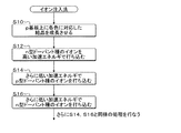
図12は、イオン注入法の適用事例を説明する図である。ここでは、図6に示した固体撮像素子20を製造する場合への適用事例で示す。イオン注入を利用する場合、そのイオン注入を繰り返し行なうことで固体撮像素子20に示す構造を作製できる。
<Ion implantation method>
FIG. 12 is a diagram for explaining an application example of the ion implantation method. Here, an example of application to the case of manufacturing the solid-state imaging device 20 shown in FIG. When ion implantation is used, the structure shown in the solid-state imaging device 20 can be manufactured by repeatedly performing the ion implantation.
たとえばp基板上に各色に対応した結晶を成長させた後に(S10)、n型ドーパント種のイオンを高い加速エネルギで打ち込む(S12)。さらに、それより低い加速エネルギでp型ドーパント種のイオンを打ち込み(S14)、さらにそれより低い加速エネルギでn型ドーパント種のイオンを打ち込む(S16)。さらに、S14,S16と同様の処理を行なう。このように、加速エネルギが順次低くなるように変化させることで、イオンの打ち込みの深さを変えることができ、結果的に、図6に示した固体撮像素子20のような構造ができる。 For example, after growing a crystal corresponding to each color on a p-substrate (S10), ions of n-type dopant species are implanted with high acceleration energy (S12). Further, ions of p-type dopant species are implanted at a lower acceleration energy (S14), and ions of n-type dopant species are implanted at a lower acceleration energy (S16). Further, processing similar to S14 and S16 is performed. In this way, by changing the acceleration energy so as to decrease sequentially, the depth of ion implantation can be changed, and as a result, a structure like the solid-state imaging device 20 shown in FIG. 6 can be obtained.
<熱拡散法>
図13は、熱拡散法の適用事例を説明する図である。ここでは、図6に示した固体撮像素子20を製造する製造プロセス(特に不純物拡散プロセス)への適用事例で示す。熱拡散を利用する場合にも、イオン注入法と同様に、熱拡散を繰り返し行なうことで固体撮像素子20に示す構造を作製できる。
<Thermal diffusion method>
FIG. 13 is a diagram for explaining an application example of the thermal diffusion method. Here, an example of application to a manufacturing process (particularly an impurity diffusion process) for manufacturing the solid-state imaging device 20 shown in FIG. 6 is shown. Even when thermal diffusion is used, the structure shown in the solid-state imaging device 20 can be manufactured by repeatedly performing thermal diffusion, as in the ion implantation method.
不純物を熱拡散させてn型層やp型層を得る場合、拡散領域を同じマスクを用いて順次p型とn型不純物を拡散させるプロセス工程を経ることで製造してもよい。このようなプロセス工程にすれば、プロセス上簡便であり、コストの低減を図ることができる。 When an n-type layer or a p-type layer is obtained by thermally diffusing impurities, the diffusion region may be manufactured through a process step of sequentially diffusing p-type and n-type impurities using the same mask. With such a process step, the process is simple and the cost can be reduced.
たとえば、図13に示すように、同じ酸化膜マスクを用いて、p型ドーパントとn型ドーパントとを順次熱拡散させることでも複数(多層)のフォトダイオード領域の形成が可能となる。したがってプロセス上簡便であり、コストの低減が図られる。 For example, as shown in FIG. 13, a plurality (multilayer) of photodiode regions can be formed by sequentially thermally diffusing a p-type dopant and an n-type dopant using the same oxide film mask. Therefore, the process is simple and the cost can be reduced.
特に、図6に示した固体撮像素子20のようなバームクーヘン状の層構造を持つ場合には、3原色の光電変換素子(フォトダイオード)用の各検知層22,24,26の全てを形成するためのマスクを1つにして共通にすることができる。 In particular, in the case of a Baumkuchen-like layer structure like the solid-state imaging device 20 shown in FIG. 6, all the detection layers 22, 24 and 26 for the three primary color photoelectric conversion elements (photodiodes) are formed. Therefore, a single mask can be used in common.
<CVD法>
図14〜図16は、CVD法の適用事例を説明する図である。ここで、図14は、CVD法の処理手順を示すフローチャートであり、図15は、製造される固体撮像素子の層構造を示す模式図であり、図16は、固体撮像素子の層構造の最終形態を示す模式図である。なお、ここでは、Si/SiGeC系量子井戸を持つ図6に示したような固体撮像素子20への適用事例で示す。
<CVD method>
14-16 is a figure explaining the application example of CVD method. Here, FIG. 14 is a flowchart showing the processing procedure of the CVD method, FIG. 15 is a schematic diagram showing the layer structure of the solid-state image sensor to be manufactured, and FIG. 16 is the final layer structure of the solid-state image sensor. It is a schematic diagram which shows a form. Here, an application example to the solid-state imaging device 20 as shown in FIG. 6 having a Si / SiGeC quantum well is shown.
図14に示すように、n型のSi基板上にCVD法を用いてSiGeC層(組成比1:0.2:1)の結晶を成長させる(S20)。たとえば、先ず、Si基板をNH4 OH,H 2 O2 ,H2 O(1:1:5)混合液に10分間浸すことで表面洗浄した後に(S21)、HF(HF:H2 O=1:50)処理を10秒行なうことで自然酸化膜を除去する(S22)。このような工程を経ることで、表面を清浄化することができ、その後の結晶成長の結晶性を向上させることができる。 As shown in FIG. 14, a SiGeC layer (composition ratio 1: 0.2: 1) crystal is grown on an n-type Si substrate by CVD (S20). For example, first, after cleaning the surface by immersing the Si substrate in a mixed solution of NH 4 OH, H 2 O 2 , H 2 O (1: 1: 5) for 10 minutes (S21), HF (HF: H 2 O = 1:50) The natural oxide film is removed by performing the process for 10 seconds (S22). Through such a process, the surface can be cleaned and the crystallinity of subsequent crystal growth can be improved.
次に、このSi基板を用意して基板ホルダーに設置する(S23)。さらに、圧力1×10⁴ Paで基板温度を1150℃でH2 ガスを1リットル/minの条件でモノシランSiH4 とC3 H8 とGeH4 をそれぞれ36μmol/minと59μmol/minと5μmol/minの条件で同時供給することでSiGeC結晶をSi基板に10nmの厚みで成長させる(S24)。 Next, this Si substrate is prepared and placed on the substrate holder (S23). Further, monosilane SiH 4 , C 3 H 8, and GeH 4 were mixed at 36 μmol / min, 59 μmol / min, and 5 μmol / min, respectively, under the conditions of a pressure of 1 × 10 4 Pa, a substrate temperature of 1150 ° C., and H 2 gas of 1 liter / min. The SiGeC crystal is grown on the Si substrate with a thickness of 10 nm by simultaneously supplying under the conditions (S24).
その後に、SiH4 のみを供給することでSi量子井戸層を1.1nmほど成長させる(S26)。 Thereafter, by supplying only SiH 4 , the Si quantum well layer is grown by about 1.1 nm (S26).
これを繰り返して、トータルの厚みが3μmになるようにすることで、緑色検知量子井戸領域を作製する(S28)。 This process is repeated so that the total thickness becomes 3 μm, thereby producing a green color detection quantum well region (S28).
さらに同様の手順により、SiGeC層(組成比1:0.2:1)を10nmとSi量子井戸層が0.95nmの厚みになるように繰り返してトータルな厚みが2μmになるように青色検知量子井戸領域を作製する(S34〜S38)。 Further, by the same procedure, the blue detection quantum is changed so that the total thickness becomes 2 μm by repeating the SiGeC layer (composition ratio 1: 0.2: 1) so that the thickness is 10 nm and the Si quantum well layer is 0.95 nm. A well region is formed (S34 to S38).
これにより、図15に示すような量子井戸の積層構造を製造することができる。なお、図15は、図5に示した量子井戸の積層構造を簡略して示したものである。 As a result, a multilayer structure of quantum wells as shown in FIG. 15 can be manufactured. FIG. 15 is a simplified illustration of the quantum well stack structure shown in FIG.
この後、たとえば熱拡散法を適用して、p型とn型のドーパントであるボロンPとリンPを所定の深さで、交互に拡散させる(S40)。また、必要に応じて、最後の最表面に、ボロンBをドーピングして、p型Si領域26P+を形成することで、暗電流を低減化させる構造にするとよい(S42)。
Thereafter, for example, by applying a thermal diffusion method, boron P and phosphorus P, which are p-type and n-type dopants, are alternately diffused at a predetermined depth (S40). Further, if necessary, it is preferable to form a p-
こうすることで、図16に示すように、緑色検知層24と青色検知層26については、Si/SiGeC系の多層量子井戸構造中に、n型Si領域24N,26Nとp型Si領域24P,26Pを形成することができる。なお、図6に示したものとの対比では、Si基板21をp型からn型に変更しているため、赤色検知層22内に、p型Si領域22Pを形成している。
As a result, as shown in FIG. 16, the green detection layer 24 and the blue detection layer 26 have n-
なお、ここではCVD法を用いたが、たとえばレーザアブレーション法では、ターゲット材料にSiGeCを用いて結晶成長させることも可能である。 Although the CVD method is used here, for example, in the laser ablation method, it is also possible to grow a crystal using SiGeC as a target material.
<MBE法>
図17〜図19は、MBE法の適用事例を説明する図である。ここで、図17は、MBE法の処理手順を示すフローチャートであり、図18は、製造される固体撮像素子の層構造を示す模式図であり、図19は、固体撮像素子の層構造の最終形態を示す模式図である。なお、ここでは、ZnCdSe/ZnSSe系量子井戸を持つ図6に示したような固体撮像素子20への適用事例で示す。
<MBE method>
17 to 19 are diagrams illustrating application examples of the MBE method. Here, FIG. 17 is a flowchart showing the processing procedure of the MBE method, FIG. 18 is a schematic diagram showing the layer structure of the solid-state imaging device to be manufactured, and FIG. 19 shows the final layer structure of the solid-state imaging device. It is a schematic diagram which shows a form. Here, an example of application to the solid-state imaging device 20 as shown in FIG. 6 having a ZnCdSe / ZnSSe quantum well is shown.
図17に示すように、n型のGaAs基板31上にMBE法を用いて、Zn0.94S0.06Se層とZn0.1 Cd0.9 Se層をそれぞれ10nmと6.0nmの厚みになるようにシャッタを用いて交互に成長させる(S50R)。このときのバンドギャップEgは1.99eVに対応する。これを繰り返して、この量子井戸構造全体の厚みが3μmになるようにすることで、赤色検知量子井戸領域(赤色検知領域32)を作製する(S52R)。
As shown in FIG. 17, an MBE method is used on an n-
さらに同様の手順により、緑色検知量子井戸領域(緑色検知領域34)と青色検知量子井戸領域(青色検知領域36)とを順次作製する。たとえば、同じくMBE法を用いて、Zn0.94S0.06Se層とZn0.1 Cd0.9 Se層をそれぞれ10nmと3.2nmの厚みになるようにシャッタを用いて交互に成長させる(S50G)。このときのバンドギャップEgは2.21eVに対応する。これを繰り返して、この量子井戸構造全体の厚みが2μmになるようにすることで、緑色検知量子井戸領域を作製する(S52G)。 Further, a green detection quantum well region (green detection region 34) and a blue detection quantum well region (blue detection region 36) are sequentially manufactured by the same procedure. For example, using the MBE method, a Zn 0.94 S 0.06 Se layer and a Zn 0.1 Cd 0.9 Se layer are alternately grown using a shutter so as to have thicknesses of 10 nm and 3.2 nm, respectively (S50G). The band gap Eg at this time corresponds to 2.21 eV. This process is repeated so that the total thickness of the quantum well structure is 2 μm, thereby producing a green color detection quantum well region (S52G).
また、同じくMBE法を用いて、Zn0.94S0.06Se層とZn0.1 Cd0.9 Se層をそれぞれ10nmと2.4nmの厚みになるようにシャッタを用いて交互に成長させる(S50B)。このときのバンドギャップEgは2.49eVに対応する。これを繰り返して、この量子井戸構造全体の厚みが1.5μmになるようにすることで、青色検知量子井戸領域を作製する(S52B)。 Similarly, using the MBE method, a Zn 0.94 S 0.06 Se layer and a Zn 0.1 Cd 0.9 Se layer are alternately grown using a shutter so as to have thicknesses of 10 nm and 2.4 nm, respectively (S50B). The band gap Eg at this time corresponds to 2.49 eV. The blue detection quantum well region is fabricated by repeating this so that the thickness of the entire quantum well structure becomes 1.5 μm (S52B).
これにより、図18に示すような量子井戸の積層構造を製造することができる。なお、図18は、図10に示した量子井戸の積層構造を簡略して示したものである。 As a result, a stacked structure of quantum wells as shown in FIG. 18 can be manufactured. FIG. 18 is a simplified illustration of the quantum well stack structure shown in FIG.
この後、たとえば熱拡散法を適用して、p型とn型のドーパントであるリンPと塩素CLを所定の深さで、交互に拡散させる(S54)。また、必要に応じて、最後の最表面に、リンPをドーピングして、p型Si領域36P+を形成することで、暗電流を低減化させる構造にするとよい(S56)。
Thereafter, for example, by applying a thermal diffusion method, phosphorus P and chlorine CL, which are p-type and n-type dopants, are alternately diffused at a predetermined depth (S54). Further, if necessary, it is preferable to form a p-
こうすることで、図19に示すように、赤色検知層22と緑色検知層24と青色検知層26について、ZnCdSe/ZnSSe系の多層量子井戸構造中に、n型Si領域22N,24N,26Nとp型Si領域22P,24P,26Pを形成することができる。なお、図16に示したものとの対比では、図16のSi基板21をn型のGaAs基板21に変更した構造であり、結果的には、赤色検知層22の下部に、GaAs基板21が設けられた構造となっている。
By doing so, as shown in FIG. 19, the red detection layer 22, the green detection layer 24, and the blue detection layer 26 have n-
なお、ここではMBE法を用いたが、たとえばMOCVD法を用いても、同様な構造が作製可能である。 Note that although the MBE method is used here, a similar structure can be produced even by using, for example, the MOCVD method.
また、何れの製法においても、最後に、図6などに示した読出回路のように、CMOS構造を通常のプロセスで作製して固体撮像素子とする。 In any of the manufacturing methods, finally, as in the readout circuit shown in FIG. 6 and the like, a CMOS structure is manufactured by a normal process to form a solid-state imaging device.
これらの固体撮像素子は、半導体層に対して深さ方向にR,G,Bの色分離用の層を持つ縦型構造のイメージセンサとなり、色フィルタなしで3原色の分離が可能になる。 These solid-state imaging devices are image sensors having a vertical structure having R, G, and B color separation layers in the depth direction with respect to the semiconductor layer, and can separate the three primary colors without color filters.
以上説明したように、本実施形態によれば、バンドギャップを制御することで色分別をする層を形成するようにした。また、特に、結晶性を考慮して素子構造を規定するようにした。このため、超格子層の結晶欠陥の発生を抑えることができるようになり、結晶欠陥に起因した様々な問題、たとえば、暗電流や光散乱を抑えることができるようになり、ノイズの少ない画像を得ることができるようになる。 As described above, according to the present embodiment, the layer for color separation is formed by controlling the band gap. In particular, the element structure is defined in consideration of crystallinity. As a result, the occurrence of crystal defects in the superlattice layer can be suppressed, and various problems caused by the crystal defects, such as dark current and light scattering, can be suppressed. Be able to get.
もちろん、バンドギャップを制御することで色分別をする層を備えるイメージセンサとしたことによる効果を享受できる。たとえば、減色フィルタを使うことなく波長分離(色分離)が実現できる。この結果、各波長に対応した検知層を、半導体層の縦方向(深さ方向)に並べることができ、面方向に波長別(色別)の画素を並べる従来の構造に比べて、事実上、画素サイズを大きくすることができ、単位面積当たりに入射する光量を多くすることができるようになり、光−電気信号の変換効率を高くでき、高い感度特性が得られるようになる。 Of course, the effect of having an image sensor provided with a layer for color separation by controlling the band gap can be enjoyed. For example, wavelength separation (color separation) can be realized without using a subtractive color filter. As a result, the detection layer corresponding to each wavelength can be arranged in the vertical direction (depth direction) of the semiconductor layer, which is practically compared to the conventional structure in which pixels by wavelength (by color) are arranged in the plane direction. The pixel size can be increased, the amount of incident light per unit area can be increased, the conversion efficiency of the optical-electrical signal can be increased, and high sensitivity characteristics can be obtained.
また、検知層を半導体層の縦方向(深さ方向)に並べることができるので、事実上、波長別に画素を設ける必要がなく、1つの画素で、複数の波長を分離して検知することができるようになる。この結果、高密度画素数のセンサを実現するのが容易になる。もちろん、色フィルタが不要であるために、低コストになる。 In addition, since the detection layer can be arranged in the vertical direction (depth direction) of the semiconductor layer, it is virtually unnecessary to provide a pixel for each wavelength, and a single pixel can be detected by separating a plurality of wavelengths. become able to. As a result, it becomes easy to realize a sensor having a high density of pixels. Of course, since no color filter is required, the cost is reduced.
また、波長による吸収係数の違いを利用したセンサでは、たとえば青色光を検知する層では赤色光や緑色光が通過するときにある程度吸収を受けるために混色が生じ色の識別能が低下するが、バンドギャップを利用した構造の場合には、この混色の問題を解消することができ十分な色再現性を得ることができる。これにより、信号処理で混色の補正を行なう必要がなく、その分の回路を省くことができ、低コストになる。 In addition, in a sensor that uses the difference in absorption coefficient depending on the wavelength, for example, in a layer that detects blue light, when red light or green light passes, it is absorbed to some extent, resulting in color mixing and a decrease in color discrimination ability. In the case of the structure using the band gap, this color mixing problem can be solved and sufficient color reproducibility can be obtained. As a result, it is not necessary to correct the color mixture by signal processing, the corresponding circuit can be omitted, and the cost is reduced.
以上、本発明を実施形態を用いて説明したが、本発明の技術的範囲は上記実施形態に記載の範囲には限定されない。発明の要旨を逸脱しない範囲で上記実施形態に多様な変更または改良を加えることができ、そのような変更または改良を加えた形態も本発明の技術的範囲に含まれる。 As mentioned above, although this invention was demonstrated using embodiment, the technical scope of this invention is not limited to the range as described in the said embodiment. Various changes or improvements can be added to the above-described embodiment without departing from the gist of the invention, and embodiments to which such changes or improvements are added are also included in the technical scope of the present invention.
また、上記の実施形態は、クレーム(請求項)にかかる発明を限定するものではなく、また実施形態の中で説明されている特徴の組合せの全てが発明の解決手段に必須であるとは限らない。前述した実施形態には種々の段階の発明が含まれており、開示される複数の構成要件における適宜の組合せにより種々の発明を抽出できる。実施形態に示される全構成要件から幾つかの構成要件が削除されても、効果が得られる限りにおいて、この幾つかの構成要件が削除された構成が発明として抽出され得る。 Further, the above embodiments do not limit the invention according to the claims (claims), and all combinations of features described in the embodiments are not necessarily essential to the solution means of the invention. Absent. The embodiments described above include inventions at various stages, and various inventions can be extracted by appropriately combining a plurality of disclosed constituent elements. Even if some constituent requirements are deleted from all the constituent requirements shown in the embodiment, as long as an effect is obtained, a configuration from which these some constituent requirements are deleted can be extracted as an invention.
<<4色以上の分光>>
たとえば、上記実施形態では、可視光帯をB,G,Rの3原色の波長成分に分けることについて述べたが、実際には1画素内で半導体層の縦方向に形成されるフォトダイオード群に設ける色別の検知層(事実上の光電変換素子)をさらに分別することで、さらに細かく分光できるようになるから、4色以上の多色の検知が可能となる。この場合、従来の3原色方式の撮像ではできなかった正確な色の情報を検知できるようになる。すなわち、4色以上の多色に分けて検知することも可能であり、赤、緑、および青以外の分光色の成分を増やすほど、より正確な情報を得ることができるようになる。
<< Spectra of four or more colors >>
For example, in the above-described embodiment, the visible light band is divided into the wavelength components of the three primary colors B, G, and R. Actually, however, in the photodiode group formed in the vertical direction of the semiconductor layer in one pixel. By further separating the detection layers (virtual photoelectric conversion elements) for each color to be provided, it becomes possible to perform finer spectroscopic analysis, so that it is possible to detect four or more colors. In this case, it is possible to detect accurate color information that could not be obtained by conventional three-primary-color imaging. That is, it is also possible to detect separately in four or more colors, and more accurate information can be obtained as the spectral color components other than red, green, and blue are increased.
3原色だけの撮像方式では色度図上で3原色のそれぞれの原点で構成される三角形より外側のところを検出することができない。これに対して、三角形の外側の色成分を検知する第4色(あるいはそれ以上)用の検知層を配してフォトダイオード群内において色を細かく分光することで、三角形の外側での正確な色を検知できることになる。したがってディスプレイ側でその信号を再生した場合、色再現もより正確に行なわれることになる。さらにディスプレイ側にも4色以上の多色表示システムを用いるとさらに正確でかつ色度図上の色再現範囲の広い映像が得られることになる。 In an imaging method using only the three primary colors, it is impossible to detect a portion outside the triangle formed by the origins of the three primary colors on the chromaticity diagram. On the other hand, by disposing a detection layer for the fourth color (or higher) that detects the color component outside the triangle and finely dispersing the color within the photodiode group, it is possible to accurately detect the color component outside the triangle. Color can be detected. Therefore, when the signal is reproduced on the display side, color reproduction is performed more accurately. Furthermore, if a multi-color display system of four or more colors is used on the display side, a more accurate image with a wide color reproduction range on the chromaticity diagram can be obtained.
たとえば、赤(R),緑(G),青(B)の3色を感知するため各検知層に加えて、第4色としてエメラルド(E)を感知するため検知層を配して、4色の分光を行なう構成とすることもできる。エメラルドは、波長的には青色と緑色との間に位置し、青色光と緑色光との間に分光されるので、フォトダイオード群内において、青色光を検知する検知層と緑色光を検知する検知層との間に、エメラルド光を検知する検知層を配置するようにすればよい。 For example, in addition to each detection layer to detect three colors of red (R), green (G), and blue (B), a detection layer is provided to detect emerald (E) as a fourth color. It can also be configured to perform color spectroscopy. The emerald is located between blue and green in terms of wavelength and is split between blue light and green light. Therefore, in the photodiode group, a detection layer that detects blue light and green light is detected. What is necessary is just to arrange | position the detection layer which detects emerald light between a detection layer.
この場合、カラー画素に色再現性を高めるために第4のカラー画素Eが加わったものであり、全体の動作は、上記説明と全く同様にすることができ、上記で述べたと同様の効果を享受することができる。この4色の場合、より正確な情報を得ることができ、このセンサを用いて検出したイメージ像を信号に変換して、さらにディスプレイ側でその信号を再生した場合、色再現も正確に行なわれる。さらにディスプレイ側にも4色以上の多色表示システムを用いると正確でかつ色再現範囲の広い映像が得られる。 In this case, the fourth color pixel E is added to the color pixel in order to improve the color reproducibility, and the overall operation can be made exactly the same as described above, and the same effect as described above can be obtained. You can enjoy it. In the case of these four colors, more accurate information can be obtained. When an image image detected using this sensor is converted into a signal and the signal is reproduced on the display side, color reproduction is also performed accurately. . Furthermore, if a multi-color display system of four or more colors is used on the display side, an accurate video with a wide color reproduction range can be obtained.
色信号処理についての詳細な説明は割愛するが、4色分の検知層に対応して、4色で撮影された各色の画素信号から、人間の目に近いRGBの3色を作り出すためのマトリックス演算を行なう画像処理プロセッサを設ける。赤(R),緑(G),青(B)に加えてエメラルド(E)をも検知するようにすれば、R,G,Bの3色での検知よりも色再現の差を低減させることができ、たとえば青緑色や赤色の再現性を向上させることができる。 Although a detailed description of the color signal processing is omitted, a matrix for generating three colors of RGB close to the human eye from pixel signals of each color photographed in four colors corresponding to the detection layers for four colors. An image processor for performing the calculation is provided. If emerald (E) is detected in addition to red (R), green (G), and blue (B), the difference in color reproduction is reduced as compared with detection with three colors of R, G, and B. For example, the reproducibility of blue-green or red can be improved.
<<可視光帯以外の分光>>
さらに上述の技術は必ずしも可視光帯内での複数の波長成分への分光に限った技術ではない。構造を最適化すれば、減色フィルタを用いずに、赤外光や紫外光の分光や検知も可能となる。この場合、たとえば可視光とともに赤外光や紫外光も同時に検出してイメージ化できる。また、同時に検出する可視光については、分光せずにモノクロ画像を検知することに限らず、上述のようにして可視光帯内をたとえば3原色成分に分光することでカラー画像を検知することもできる。これによって眼で見ることができる可視光のイメージ像(モノクロ画像あるいはカラー画像)と対応して、眼で見ることのできない赤外光や紫外光の像情報を同時に取得することができる。これによって暗視カメラや光合成監視カメラなどの新しい情報システムのキーデバイスとして応用が広がる。
<< Spectra other than visible light band >>
Furthermore, the above-described technique is not necessarily limited to the spectroscopy to a plurality of wavelength components in the visible light band. If the structure is optimized, infrared light and ultraviolet light can be separated and detected without using a subtractive color filter. In this case, for example, infrared light and ultraviolet light can be detected and imaged together with visible light. For visible light detected at the same time, it is not limited to detecting a monochrome image without splitting, but a color image can also be detected by splitting the visible light band into, for example, three primary color components as described above. it can. Accordingly, image information of infrared light and ultraviolet light that cannot be seen by the eyes can be simultaneously acquired in correspondence with an image image (monochrome image or color image) of visible light that can be seen by the eyes. This expands the application as a key device for new information systems such as night vision cameras and photosynthetic surveillance cameras.
11,21…Si基板、12,32…赤色検知領域、14,34…緑色検知領域、16,36…青色検知領域、20…固体撮像素子、22…赤色検知層、24…緑色検知層、6…青色検知層、31…GaAs基板、105…電荷−電圧信号変換部、132…電荷生成部、136…リセットトランジスタ、138…フローティングディフュージョン、140…読出線選択用トランジスタ、142…増幅用トランジスタ 11, 21 ... Si substrate, 12, 32 ... red detection area, 14, 34 ... green detection area, 16, 36 ... blue detection area, 20 ... solid-state image sensor, 22 ... red detection layer, 24 ... green detection layer, 6 DESCRIPTION OF SYMBOLS ... Blue detection layer, 31 ... GaAs substrate, 105 ... Charge-voltage signal conversion part, 132 ... Charge generation part, 136 ... Reset transistor, 138 ... Floating diffusion, 140 ... Read-out line selection transistor, 142 ... Amplification transistor
Claims (6)
前記複数の検知領域は、前記光の入射面から深さ方向に、複数の光をそれぞれ選択的に吸収可能に前記光の波長に応じて、バンドギャップが異なる複数の検知領域として形成されており、
前記複数の検知領域のバンドギャップは、前記光の入射面の入射面から遠ざかるにつれて狭くなっており、
前記各検知領域は、
Siを含む三元以上の混晶系の組成比を変化させて前記各検知領域のバンドギャップを制御することにより、前記基板と格子整合条件に適合するように構成され、
量子井戸構造を有する、
ことを特徴とする、
物理情報取得装置。 Each of the wavelengths of the electromagnetic wave includes a plurality of detection regions stacked in a depth direction from a light incident surface facing the substrate on a predetermined substrate, and the electromagnetic waves are separated and detected in each detection region. A physical information acquisition device for detecting a physical quantity distribution that outputs a unit signal corresponding to
The plurality of detection regions are formed as a plurality of detection regions having different band gaps depending on the wavelength of the light so that the plurality of light can be selectively absorbed in the depth direction from the light incident surface. ,
The band gaps of the plurality of detection regions are narrowed away from the incident surface of the light incident surface,
Each detection area is
By controlling the bandgap of the respective detection regions by changing the composition ratio of the ternary or higher mixed crystal containing Si, it is configured to fit the substrate lattice matching condition,
Having a quantum well structure,
It is characterized by
Physical information acquisition device.
ことを特徴とする、
請求項1に記載の物理情報取得装置。 The detection region has a superlattice structure,
The physical information acquisition apparatus according to claim 1.
請求項1に記載の物理情報取得装置。 The detection region is configured to meet the lattice matching condition by a mixed crystal of SiC mixed with Ge, and has a quantum well structure.
The physical information acquisition apparatus according to claim 1.
請求項3に記載の物理情報取得装置。 The detection region has a thin film of a superlattice layer having a lattice constant different from that of Si at an interface between Si and SiC or a SiGeC-based layer.
The physical information acquisition apparatus according to claim 3.
前記複数の検知領域は、前記光の入射面から深さ方向に、複数の光をそれぞれ選択的に吸収可能に前記光の波長に応じて、バンドギャップが異なる複数の検知領域として形成され、
前記複数の検知領域のバンドギャップは、前記光の入射面の入射面から遠ざかるにつれて狭くなっており、
前記各検知領域は、
Siを含む三元以上の混晶系の組成比を変化させて前記各検知領域のバンドギャップを制御することにより、前記基板と格子整合条件に適合するように構成され、
量子井戸構造を有する
ように形成した、
ことを特徴とする、物理情報取得装置の製造方法。 Each of the wavelengths of the electromagnetic wave includes a plurality of detection regions stacked in a depth direction from a light incident surface facing the substrate on a predetermined substrate, and the electromagnetic waves are separated and detected in each detection region. A method for manufacturing a physical information acquisition device for detecting a physical quantity distribution that outputs a unit signal corresponding to
The plurality of detection regions are formed as a plurality of detection regions having different band gaps depending on the wavelength of the light so that the plurality of light can be selectively absorbed in the depth direction from the light incident surface, respectively.
The band gaps of the plurality of detection regions are narrowed away from the incident surface of the light incident surface,
Each detection area is
By controlling the bandgap of the respective detection regions by changing the composition ratio of the ternary or higher mixed crystal containing Si, it is configured to fit the substrate lattice matching condition,
Formed to have a quantum well structure,
A method for manufacturing a physical information acquisition apparatus, characterized in that:
イオン注入を繰り返すことにより形成する、
熱拡散を繰り返すことにより形成する、
複数回のCVD法で結晶成長を行なうことにより形成する、
複数回のMBE法あるいはMOCVD法を行なうことにより形成する
ことを特徴とする、
請求項5に記載の物理情報取得装置の製造方法。 The plurality of detection regions are formed by any of the following methods:
Formed by repeating ion implantation,
Formed by repeating thermal diffusion,
It is formed by performing crystal growth by a plurality of CVD methods.
It is formed by performing MBE method or MOCVD method multiple times.
The manufacturing method of the physical information acquisition apparatus of Claim 5.
Priority Applications (1)
| Application Number | Priority Date | Filing Date | Title |
|---|---|---|---|
| JP2005055483A JP5369362B2 (en) | 2005-03-01 | 2005-03-01 | Physical information acquisition apparatus and manufacturing method thereof |
Applications Claiming Priority (1)
| Application Number | Priority Date | Filing Date | Title |
|---|---|---|---|
| JP2005055483A JP5369362B2 (en) | 2005-03-01 | 2005-03-01 | Physical information acquisition apparatus and manufacturing method thereof |
Publications (3)
| Publication Number | Publication Date |
|---|---|
| JP2006245088A JP2006245088A (en) | 2006-09-14 |
| JP2006245088A5 JP2006245088A5 (en) | 2007-12-27 |
| JP5369362B2 true JP5369362B2 (en) | 2013-12-18 |
Family
ID=37051232
Family Applications (1)
| Application Number | Title | Priority Date | Filing Date |
|---|---|---|---|
| JP2005055483A Expired - Fee Related JP5369362B2 (en) | 2005-03-01 | 2005-03-01 | Physical information acquisition apparatus and manufacturing method thereof |
Country Status (1)
| Country | Link |
|---|---|
| JP (1) | JP5369362B2 (en) |
Families Citing this family (8)
| Publication number | Priority date | Publication date | Assignee | Title |
|---|---|---|---|---|
| JP2008172020A (en) * | 2007-01-11 | 2008-07-24 | Rohm Co Ltd | Semiconductor photodetector |
| JP5444899B2 (en) | 2008-09-10 | 2014-03-19 | ソニー株式会社 | Solid-state imaging device manufacturing method and solid-state imaging device manufacturing substrate |
| US8665363B2 (en) | 2009-01-21 | 2014-03-04 | Sony Corporation | Solid-state image device, method for producing the same, and image pickup apparatus |
| JP5509962B2 (en) | 2010-03-19 | 2014-06-04 | ソニー株式会社 | Solid-state imaging device, manufacturing method thereof, and electronic apparatus |
| JP5585232B2 (en) | 2010-06-18 | 2014-09-10 | ソニー株式会社 | Solid-state imaging device, electronic equipment |
| CN104583760A (en) * | 2012-02-21 | 2015-04-29 | 麻省理工学院 | Spectrometer device |
| US11411039B2 (en) * | 2020-05-19 | 2022-08-09 | Applied Materials, Inc. | Stacked pixel structure formed using epitaxy |
| JPWO2021261093A1 (en) * | 2020-06-24 | 2021-12-30 |
Family Cites Families (5)
| Publication number | Priority date | Publication date | Assignee | Title |
|---|---|---|---|---|
| JP2995744B2 (en) * | 1989-03-23 | 1999-12-27 | 日本電気株式会社 | Photo detector |
| JPH04280678A (en) * | 1991-03-08 | 1992-10-06 | Nec Corp | Solid-state image pickly element |
| JP3987364B2 (en) * | 2002-04-02 | 2007-10-10 | 日本放送協会 | Stacked solid-state imaging device and signal readout method thereof |
| JP4154165B2 (en) * | 2002-04-05 | 2008-09-24 | キヤノン株式会社 | PHOTOELECTRIC CONVERSION ELEMENT, SOLID-STATE IMAGING DEVICE, CAMERA, AND IMAGE READING DEVICE USING THE SAME |
| JP2006066456A (en) * | 2004-08-24 | 2006-03-09 | Fuji Photo Film Co Ltd | Solid-state image sensor |
-
2005
- 2005-03-01 JP JP2005055483A patent/JP5369362B2/en not_active Expired - Fee Related
Also Published As
| Publication number | Publication date |
|---|---|
| JP2006245088A (en) | 2006-09-14 |
Similar Documents
| Publication | Publication Date | Title |
|---|---|---|
| JP5609119B2 (en) | Solid-state imaging device, manufacturing method thereof, and imaging device | |
| US8101901B2 (en) | Method and apparatus for acquiring physical information, method for manufacturing semiconductor device including array of a plurality of unit components for detecting physical quantity distribution, light-receiving device and manufacturing method therefor, and solid-state imaging device and manufacturing method therefor | |
| US9142584B2 (en) | Solid-state imaging device with pixel isolation portion, method for manufacturing solid-state imaging device, and electronic apparatus | |
| TWI596747B (en) | Solid-state imaging device and electronic equipment | |
| US8665363B2 (en) | Solid-state image device, method for producing the same, and image pickup apparatus | |
| JP2010093229A (en) | Method for manufacturing solid-state imaging apparatus, solid-state imaging apparatus, and manufacturing substrate for solid-state imaging apparatus | |
| JP2014127519A (en) | Solid-state imaging element and electronic device | |
| KR101579548B1 (en) | Passivated upstanding nanostructures and methods of making the same | |
| JP2015119018A (en) | Solid-state imaging device and electronic device | |
| JP2015220339A (en) | Solid-state imaging device | |
| JP5369362B2 (en) | Physical information acquisition apparatus and manufacturing method thereof | |
| TWI455296B (en) | Solid-state imaging device, manufacturing method thereof, and electronic device | |
| US20150255501A1 (en) | Solid state imaging device and method of fabricating the same | |
| CN101794836B (en) | Solid-state image device, method for producing the same, and image pickup apparatus | |
| JP2006032670A (en) | Semiconductor light receiving element and manufacturing method thereof | |
| CN1943042A (en) | Vertical color filter sensor group with carrier-collector elements | |
| JP6520326B2 (en) | Imaging device and imaging device | |
| JP2012094714A (en) | Solid-state imaging device and method of manufacturing the same | |
| CN1943041A (en) | Vertical color filter sensor group | |
| Rehm et al. | Advanced III/V quantum-structure devices for high performance infrared focal plane arrays |
Legal Events
| Date | Code | Title | Description |
|---|---|---|---|
| A521 | Request for written amendment filed |
Free format text: JAPANESE INTERMEDIATE CODE: A523 Effective date: 20071113 |
|
| A621 | Written request for application examination |
Free format text: JAPANESE INTERMEDIATE CODE: A621 Effective date: 20071113 |
|
| RD02 | Notification of acceptance of power of attorney |
Free format text: JAPANESE INTERMEDIATE CODE: A7422 Effective date: 20091007 |
|
| RD04 | Notification of resignation of power of attorney |
Free format text: JAPANESE INTERMEDIATE CODE: A7424 Effective date: 20091016 |
|
| A977 | Report on retrieval |
Free format text: JAPANESE INTERMEDIATE CODE: A971007 Effective date: 20100730 |
|
| A131 | Notification of reasons for refusal |
Free format text: JAPANESE INTERMEDIATE CODE: A131 Effective date: 20110830 |
|
| A521 | Request for written amendment filed |
Free format text: JAPANESE INTERMEDIATE CODE: A523 Effective date: 20111031 |
|
| A131 | Notification of reasons for refusal |
Free format text: JAPANESE INTERMEDIATE CODE: A131 Effective date: 20120724 |
|
| A521 | Request for written amendment filed |
Free format text: JAPANESE INTERMEDIATE CODE: A523 Effective date: 20120921 |
|
| A131 | Notification of reasons for refusal |
Free format text: JAPANESE INTERMEDIATE CODE: A131 Effective date: 20130205 |
|
| A521 | Request for written amendment filed |
Free format text: JAPANESE INTERMEDIATE CODE: A523 Effective date: 20130401 |
|
| A131 | Notification of reasons for refusal |
Free format text: JAPANESE INTERMEDIATE CODE: A131 Effective date: 20130604 |
|
| A521 | Request for written amendment filed |
Free format text: JAPANESE INTERMEDIATE CODE: A523 Effective date: 20130729 |
|
| TRDD | Decision of grant or rejection written | ||
| A01 | Written decision to grant a patent or to grant a registration (utility model) |
Free format text: JAPANESE INTERMEDIATE CODE: A01 Effective date: 20130820 |
|
| A61 | First payment of annual fees (during grant procedure) |
Free format text: JAPANESE INTERMEDIATE CODE: A61 Effective date: 20130902 |
|
| LAPS | Cancellation because of no payment of annual fees |