JP5362985B2 - Method for forming semiconductor device having void and structure formed by the method - Google Patents
Method for forming semiconductor device having void and structure formed by the method Download PDFInfo
- Publication number
- JP5362985B2 JP5362985B2 JP2007515228A JP2007515228A JP5362985B2 JP 5362985 B2 JP5362985 B2 JP 5362985B2 JP 2007515228 A JP2007515228 A JP 2007515228A JP 2007515228 A JP2007515228 A JP 2007515228A JP 5362985 B2 JP5362985 B2 JP 5362985B2
- Authority
- JP
- Japan
- Prior art keywords
- metal wiring
- wiring level
- trench
- dielectric material
- conductive material
- Prior art date
- Legal status (The legal status is an assumption and is not a legal conclusion. Google has not performed a legal analysis and makes no representation as to the accuracy of the status listed.)
- Expired - Fee Related
Links
Images


Classifications
-
- H—ELECTRICITY
- H01—ELECTRIC ELEMENTS
- H01L—SEMICONDUCTOR DEVICES NOT COVERED BY CLASS H10
- H01L21/00—Processes or apparatus adapted for the manufacture or treatment of semiconductor or solid state devices or of parts thereof
- H01L21/02—Manufacture or treatment of semiconductor devices or of parts thereof
- H01L21/04—Manufacture or treatment of semiconductor devices or of parts thereof the devices having at least one potential-jump barrier or surface barrier, e.g. PN junction, depletion layer or carrier concentration layer
- H01L21/18—Manufacture or treatment of semiconductor devices or of parts thereof the devices having at least one potential-jump barrier or surface barrier, e.g. PN junction, depletion layer or carrier concentration layer the devices having semiconductor bodies comprising elements of Group IV of the Periodic System or AIIIBV compounds with or without impurities, e.g. doping materials
- H01L21/30—Treatment of semiconductor bodies using processes or apparatus not provided for in groups H01L21/20 - H01L21/26
- H01L21/31—Treatment of semiconductor bodies using processes or apparatus not provided for in groups H01L21/20 - H01L21/26 to form insulating layers thereon, e.g. for masking or by using photolithographic techniques; After treatment of these layers; Selection of materials for these layers
- H01L21/3105—After-treatment
- H01L21/311—Etching the insulating layers by chemical or physical means
-
- H—ELECTRICITY
- H01—ELECTRIC ELEMENTS
- H01L—SEMICONDUCTOR DEVICES NOT COVERED BY CLASS H10
- H01L21/00—Processes or apparatus adapted for the manufacture or treatment of semiconductor or solid state devices or of parts thereof
- H01L21/70—Manufacture or treatment of devices consisting of a plurality of solid state components formed in or on a common substrate or of parts thereof; Manufacture of integrated circuit devices or of parts thereof
- H01L21/71—Manufacture of specific parts of devices defined in group H01L21/70
- H01L21/768—Applying interconnections to be used for carrying current between separate components within a device comprising conductors and dielectrics
- H01L21/76801—Applying interconnections to be used for carrying current between separate components within a device comprising conductors and dielectrics characterised by the formation and the after-treatment of the dielectrics, e.g. smoothing
- H01L21/7682—Applying interconnections to be used for carrying current between separate components within a device comprising conductors and dielectrics characterised by the formation and the after-treatment of the dielectrics, e.g. smoothing the dielectric comprising air gaps
-
- H—ELECTRICITY
- H01—ELECTRIC ELEMENTS
- H01L—SEMICONDUCTOR DEVICES NOT COVERED BY CLASS H10
- H01L21/00—Processes or apparatus adapted for the manufacture or treatment of semiconductor or solid state devices or of parts thereof
- H01L21/02—Manufacture or treatment of semiconductor devices or of parts thereof
- H01L21/04—Manufacture or treatment of semiconductor devices or of parts thereof the devices having at least one potential-jump barrier or surface barrier, e.g. PN junction, depletion layer or carrier concentration layer
- H01L21/18—Manufacture or treatment of semiconductor devices or of parts thereof the devices having at least one potential-jump barrier or surface barrier, e.g. PN junction, depletion layer or carrier concentration layer the devices having semiconductor bodies comprising elements of Group IV of the Periodic System or AIIIBV compounds with or without impurities, e.g. doping materials
- H01L21/28—Manufacture of electrodes on semiconductor bodies using processes or apparatus not provided for in groups H01L21/20 - H01L21/268
-
- H—ELECTRICITY
- H01—ELECTRIC ELEMENTS
- H01L—SEMICONDUCTOR DEVICES NOT COVERED BY CLASS H10
- H01L21/00—Processes or apparatus adapted for the manufacture or treatment of semiconductor or solid state devices or of parts thereof
- H01L21/02—Manufacture or treatment of semiconductor devices or of parts thereof
- H01L21/04—Manufacture or treatment of semiconductor devices or of parts thereof the devices having at least one potential-jump barrier or surface barrier, e.g. PN junction, depletion layer or carrier concentration layer
- H01L21/18—Manufacture or treatment of semiconductor devices or of parts thereof the devices having at least one potential-jump barrier or surface barrier, e.g. PN junction, depletion layer or carrier concentration layer the devices having semiconductor bodies comprising elements of Group IV of the Periodic System or AIIIBV compounds with or without impurities, e.g. doping materials
- H01L21/30—Treatment of semiconductor bodies using processes or apparatus not provided for in groups H01L21/20 - H01L21/26
- H01L21/31—Treatment of semiconductor bodies using processes or apparatus not provided for in groups H01L21/20 - H01L21/26 to form insulating layers thereon, e.g. for masking or by using photolithographic techniques; After treatment of these layers; Selection of materials for these layers
- H01L21/3105—After-treatment
- H01L21/311—Etching the insulating layers by chemical or physical means
- H01L21/31105—Etching inorganic layers
- H01L21/31111—Etching inorganic layers by chemical means
- H01L21/31116—Etching inorganic layers by chemical means by dry-etching
-
- H—ELECTRICITY
- H01—ELECTRIC ELEMENTS
- H01L—SEMICONDUCTOR DEVICES NOT COVERED BY CLASS H10
- H01L21/00—Processes or apparatus adapted for the manufacture or treatment of semiconductor or solid state devices or of parts thereof
- H01L21/02—Manufacture or treatment of semiconductor devices or of parts thereof
- H01L21/04—Manufacture or treatment of semiconductor devices or of parts thereof the devices having at least one potential-jump barrier or surface barrier, e.g. PN junction, depletion layer or carrier concentration layer
- H01L21/18—Manufacture or treatment of semiconductor devices or of parts thereof the devices having at least one potential-jump barrier or surface barrier, e.g. PN junction, depletion layer or carrier concentration layer the devices having semiconductor bodies comprising elements of Group IV of the Periodic System or AIIIBV compounds with or without impurities, e.g. doping materials
- H01L21/30—Treatment of semiconductor bodies using processes or apparatus not provided for in groups H01L21/20 - H01L21/26
- H01L21/31—Treatment of semiconductor bodies using processes or apparatus not provided for in groups H01L21/20 - H01L21/26 to form insulating layers thereon, e.g. for masking or by using photolithographic techniques; After treatment of these layers; Selection of materials for these layers
- H01L21/3205—Deposition of non-insulating-, e.g. conductive- or resistive-, layers on insulating layers; After-treatment of these layers
-
- H—ELECTRICITY
- H01—ELECTRIC ELEMENTS
- H01L—SEMICONDUCTOR DEVICES NOT COVERED BY CLASS H10
- H01L21/00—Processes or apparatus adapted for the manufacture or treatment of semiconductor or solid state devices or of parts thereof
- H01L21/70—Manufacture or treatment of devices consisting of a plurality of solid state components formed in or on a common substrate or of parts thereof; Manufacture of integrated circuit devices or of parts thereof
- H01L21/71—Manufacture of specific parts of devices defined in group H01L21/70
- H01L21/768—Applying interconnections to be used for carrying current between separate components within a device comprising conductors and dielectrics
- H01L21/76801—Applying interconnections to be used for carrying current between separate components within a device comprising conductors and dielectrics characterised by the formation and the after-treatment of the dielectrics, e.g. smoothing
- H01L21/76802—Applying interconnections to be used for carrying current between separate components within a device comprising conductors and dielectrics characterised by the formation and the after-treatment of the dielectrics, e.g. smoothing by forming openings in dielectrics
- H01L21/76807—Applying interconnections to be used for carrying current between separate components within a device comprising conductors and dielectrics characterised by the formation and the after-treatment of the dielectrics, e.g. smoothing by forming openings in dielectrics for dual damascene structures
-
- H—ELECTRICITY
- H01—ELECTRIC ELEMENTS
- H01L—SEMICONDUCTOR DEVICES NOT COVERED BY CLASS H10
- H01L23/00—Details of semiconductor or other solid state devices
- H01L23/52—Arrangements for conducting electric current within the device in operation from one component to another, i.e. interconnections, e.g. wires, lead frames
- H01L23/522—Arrangements for conducting electric current within the device in operation from one component to another, i.e. interconnections, e.g. wires, lead frames including external interconnections consisting of a multilayer structure of conductive and insulating layers inseparably formed on the semiconductor body
- H01L23/5222—Capacitive arrangements or effects of, or between wiring layers
-
- H—ELECTRICITY
- H01—ELECTRIC ELEMENTS
- H01L—SEMICONDUCTOR DEVICES NOT COVERED BY CLASS H10
- H01L23/00—Details of semiconductor or other solid state devices
- H01L23/52—Arrangements for conducting electric current within the device in operation from one component to another, i.e. interconnections, e.g. wires, lead frames
- H01L23/522—Arrangements for conducting electric current within the device in operation from one component to another, i.e. interconnections, e.g. wires, lead frames including external interconnections consisting of a multilayer structure of conductive and insulating layers inseparably formed on the semiconductor body
- H01L23/532—Arrangements for conducting electric current within the device in operation from one component to another, i.e. interconnections, e.g. wires, lead frames including external interconnections consisting of a multilayer structure of conductive and insulating layers inseparably formed on the semiconductor body characterised by the materials
- H01L23/5329—Insulating materials
- H01L23/53295—Stacked insulating layers
-
- H—ELECTRICITY
- H01—ELECTRIC ELEMENTS
- H01L—SEMICONDUCTOR DEVICES NOT COVERED BY CLASS H10
- H01L28/00—Passive two-terminal components without a potential-jump or surface barrier for integrated circuits; Details thereof; Multistep manufacturing processes therefor
- H01L28/40—Capacitors
- H01L28/60—Electrodes
- H01L28/82—Electrodes with an enlarged surface, e.g. formed by texturisation
- H01L28/86—Electrodes with an enlarged surface, e.g. formed by texturisation having horizontal extensions
- H01L28/87—Electrodes with an enlarged surface, e.g. formed by texturisation having horizontal extensions made by depositing layers, e.g. by depositing alternating conductive and insulating layers
Landscapes
- Engineering & Computer Science (AREA)
- Power Engineering (AREA)
- Computer Hardware Design (AREA)
- Microelectronics & Electronic Packaging (AREA)
- General Physics & Mathematics (AREA)
- Physics & Mathematics (AREA)
- Condensed Matter Physics & Semiconductors (AREA)
- Manufacturing & Machinery (AREA)
- Chemical & Material Sciences (AREA)
- Chemical Kinetics & Catalysis (AREA)
- General Chemical & Material Sciences (AREA)
- Inorganic Chemistry (AREA)
- Internal Circuitry In Semiconductor Integrated Circuit Devices (AREA)
- Drying Of Semiconductors (AREA)
- Formation Of Insulating Films (AREA)
Description
本発明は一般に半導体デバイスに関し、詳細には、配線レベル(配線高さ)内に空隙を有する半導体デバイスの形成方法および該方法によって形成された構造に関する。 The present invention generally relates to semiconductor devices, and more particularly to a method of forming a semiconductor device having a void in a wiring level (wiring height) and a structure formed by the method.
半導体デバイスが縮小し続けるにつれデバイス・フィーチャ間の距離は短くなる。金属配線層内においてフィーチャ間の距離が短くなると静電容量が増大する。したがって半導体デバイス業界では、デバイス・フィーチャ間の距離を短くしても低い静電容量を維持することができ、上記の問題およびその他の問題を解決する、半導体デバイスの形成方法が求められている。 As semiconductor devices continue to shrink, the distance between device features decreases. As the distance between features decreases in the metal wiring layer, the capacitance increases. Accordingly, there is a need in the semiconductor device industry for a method of forming a semiconductor device that can maintain a low capacitance even when the distance between device features is reduced and solves the above and other problems.
本発明は、金属配線レベル内に空隙を有し上述の問題を解決する半導体デバイスの形成方法および該方法によって形成された構造に関する。 The present invention relates to a method of forming a semiconductor device having a void in a metal wiring level and solving the above-mentioned problems, and a structure formed by the method.
本発明の第1の態様は、第1の誘電材料と第2の誘電材料の交互層を付着させるステップであって、第1の誘電材料と第2の誘電材料が異なる速度で選択的にエッチング可能であるステップと、誘電材料の交互層内に第1のフィーチャを形成するステップと、誘電材料の交互層を選択的にエッチングして、第1の誘電材料を有するそれぞれの層内の第1の誘電材料の全部でない少なくとも一部分を除去し、第2の誘電材料を本質的にエッチングされていないままにしておくステップとを含む、半導体デバイスの形成方法を提供する。 A first aspect of the invention is the step of depositing alternating layers of a first dielectric material and a second dielectric material, wherein the first dielectric material and the second dielectric material are selectively etched at different rates. Possible steps, forming first features in alternating layers of dielectric material, and selectively etching the alternating layers of dielectric material to provide a first in each layer having the first dielectric material. Removing at least a portion of all of the dielectric material, and leaving the second dielectric material essentially unetched.
本発明の第2の態様は、第1の絶縁材料と第2の絶縁材料の交互層を付着させるステップと、ダマシン・フィーチャを形成するステップと、第1の絶縁材料の層内に開口を形成するステップとを含む、半導体デバイスの形成方法を提供する。 A second aspect of the invention includes depositing alternating layers of first and second insulating materials, forming damascene features, and forming openings in the first layer of insulating material. And a method for forming a semiconductor device.
本発明の第3の態様は、第1の誘電材料と第2の誘電材料の交互層を有し、第1の誘電材料と第2の誘電材料の交互層内に形成された第1のフィーチャを有する金属配線レベルと、第1の誘電材料内の複数の開口とを含む半導体デバイスを提供する。 According to a third aspect of the present invention, there is provided a first feature having alternating layers of a first dielectric material and a second dielectric material, and formed in the alternating layers of the first dielectric material and the second dielectric material. A semiconductor device is provided that includes a metal interconnect level having a plurality of openings in a first dielectric material.
本発明の第4の態様は、交互層をなす複数の第1および第2の絶縁層であって、第1の絶縁層と第2の絶縁層のエッチング速度が異なる複数の絶縁層と、第1および第2の絶縁層内に形成された第1のフィーチャと、選択エッチング中に形成された複数の第1の絶縁層内の複数の開口とを含む半導体デバイスを提供する。 According to a fourth aspect of the present invention, there are provided a plurality of first and second insulating layers forming alternating layers, wherein the first insulating layer and the second insulating layer have different etching rates, and A semiconductor device is provided that includes first features formed in first and second insulating layers and a plurality of openings in the plurality of first insulating layers formed during selective etching.
本発明の上記の特徴および利点ならびに他の特徴および利点は、本発明の実施形態の以下のより詳細な説明から明白となろう。 The above features and advantages of the invention, as well as other features and advantages, will be apparent from the following more detailed description of embodiments of the invention.
次に、図面を参照して本発明の実施形態を詳細に説明する。それらの図面では同様の符号が同様の要素を指示する。 Next, embodiments of the present invention will be described in detail with reference to the drawings. In the drawings, like numerals indicate like elements.
次に、本発明のあるいくつかの実施形態を示し詳細に説明するが、それらの実施形態には、添付の請求項の範囲を逸脱しないさまざまな変更および修正を加えることができることを理解されたい。本発明の範囲は、本明細書に記載された構成要素の数、構成要素の材料、構成要素の形状、構成要素の相対的な配置等に限定されない。図面は本発明を例示することを目的としているが、それらの図面は一様な尺度で描かれているわけではない。 Next, certain embodiments of the present invention will be shown and described in detail, but it should be understood that various changes and modifications can be made to the embodiments without departing from the scope of the appended claims. . The scope of the invention is not limited to the number of components described herein, the material of the components, the shape of the components, the relative arrangement of the components, and the like. Although the drawings are intended to illustrate the present invention, the drawings are not drawn to scale.
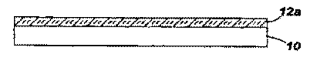
図1に、その上に第1の絶縁層12aが形成されたプリメタル誘電体(pre−metal dielectric:PMD)10の断面図を示す。PMD10はSiO2ベースの材料などの1種または数種の誘電材料、すなわちSiO2、PSG、BPSG、SiCOH(OSG)、SiLK(商標)(ダウ・ケミカル社(Dow Chemical Corp.))、SiN、SiC、SiCN、C−H等を含む。第1の絶縁層12aは誘電材料を含み、この例ではポリアリーレンエーテル(SiLK(商標))、パリレン(NまたはF)、Teflon、これらの膜の多孔質膜などの有機誘電材料を含む。使用する有機誘電材料のタイプは、使用する付着技法に応じて決定することができる。例えば、化学蒸着(CVD)またはプラズマ化学蒸着(PECVD)を使用して第1の絶縁層12aを形成する場合には、パリレン(NまたはF)、Teflonまたはこれらの膜の多孔質膜を使用することができる。しかし、スピンオン付着を使用して第1の絶縁層12aを形成する場合には、SiLK(商標)を使用することができる。第1の絶縁層12aは5〜10nmの厚さに形成することができる。
FIG. 1 shows a cross-sectional view of a pre-metal dielectric (PMD) 10 having a first
次いで、図2に示すように、第1の絶縁層12a上に第2の絶縁層14aを形成する。第2の絶縁層14aは誘電材料を含み、この例ではSiCOH(OSG)、SiO2、フッ素化SiO2(FSG)、メチルシルセスキオキサン(MSQ)、これらの材料の多孔質膜などの無機誘電材料を含む。第1の絶縁層12aと同様に、第2の絶縁層14aは、CVD、PECVD、スピンオン付着または他の同様の付着技法を使用して形成することができる。第2の絶縁層14aは5〜10nmの厚さに形成することができる。
Next, as shown in FIG. 2, a second
図3に示すように、第2の絶縁層14a上に第3の絶縁層12bを形成する。第3の絶縁層12bは第1の絶縁層12aと同様の有機誘電材料を含む。第3の絶縁層12bは第1の絶縁層12aと同様の技法を使用して形成され、第1の絶縁層12aと同様の厚さを有する。
As shown in FIG. 3, a third insulating
図4に示すように、第3の絶縁層12b上に第4の絶縁層14bを形成する。第4の絶縁層14bは第2の絶縁層14aと同様の無機誘電材料を含む。第4の絶縁層14bは第2の絶縁層14aと同様の技法を使用して形成され、第2の絶縁層14aと同様の厚さを有する。
As shown in FIG. 4, a fourth
このようにして、基板10上に、図5に示すような有機誘電材料と無機誘電材料の交互層を、第1の金属配線レベル20として望ましい厚さに形成することができる。この例では層12c〜12fが、第1および第3の絶縁層12a、12bと同様の有機誘電材料を含む。同様に層14c〜14fは、第2および第4の絶縁層14a、14bと同様の無機誘電材料を含む。本発明において描かれる層の数は単に例示のためのものであって、限定を意図したものではなく、少なくとも1つの有機層と少なくとも1つの無機層が存在すればよい。同様に、この例において有機誘電材料を最初に付着させたのは単に例示のためであることに留意されたい。最初に付着させるのは無機誘電材料でもまたは有機誘電材料でもよい。
In this way, an alternating layer of an organic dielectric material and an inorganic dielectric material as shown in FIG. 5 can be formed on the
また、この有機絶縁材料と無機絶縁材料の交互層をin−situで付着させることが望ましい場合があることにも留意されたい。例えば、単一のPECVD室を使用し、この室から外に出すことなく、無機層と有機層の両方を付着させることができる。また、スピン塗布トラックを使用し、この交互層の付着と硬化の両方を同じ室内で実施することもできる。あるいは、いずれかの技法を使用して、所望の厚さの2倍の厚さを有する第1の絶縁層12aを付着させることもできる。その後、第1の絶縁層12aをプラズマ処理または熱処理にかけ、第1の絶縁層12aの上部を、第2の絶縁層14aにおいて必要な材料に転化させる。これらの方法は、有機絶縁層と無機絶縁層の間の厚さの不ぞろいを低下させるのに役立ち、有機絶縁層と無機絶縁層の間の付着力を増大させることができる。
It should also be noted that it may be desirable to deposit the alternating layers of organic and inorganic insulating materials in-situ. For example, a single PECVD chamber can be used and both inorganic and organic layers can be deposited without leaving the chamber. It is also possible to use a spin coating track to perform both alternating layer deposition and curing in the same chamber. Alternatively, any technique can be used to deposit the first
第1の配線レベル20として望ましい厚さを達成した後、図6に示すように、第1の配線レベル20内に、第1のフィーチャ22およびこの例では第2のフィーチャ24を形成する。第1および第2のフィーチャ22、24は配線ライン用のワイヤ・トレンチであり、従来のパターン形成技法および従来のエッチング技法を使用して形成することができる。
After achieving the desired thickness for the
第1および第2のフィーチャ22、24の形成に続いて、第1の配線レベル20内の有機誘電材料の少なくとも一部分、この例では層12a〜12f内の有機誘電材料の少なくとも一部分を除去するための選択エッチングを実行する(図7)。有機誘電材料がp−SiLK(商標)を含み、無機誘電材料がp−OSGを含むこの例では、N2プラズマ、H2プラズマまたは他の同様のプラズマ・エッチングを使用して、この有機誘電材料を選択的に除去することができる。このN2またはH2エッチングは、約3〜200mTの圧力範囲において、平行プレートまたは高密度プラズマの一般的なパワーおよびフロー条件で実施することができる。あるいは、100:1DHFなどの湿式エッチング剤を使用して無機誘電材料(p−OSG)の部分をエッチングし、層12a〜12f内のSiLK(商標)材料を残してもよい。
Following formation of the first and
層12a〜12f内の有機誘電材料の選択エッチングの結果、図7に示すように開口ないし空隙26が形成される。層12a〜12fの有機誘電材料のエッチング速度は層14a〜14fの無機誘電材料のエッチング速度よりも大きいため、空隙26は、層12a〜12fの有機誘電材料内に形成され、層14a〜14fの無機誘電材料内には形成されない。第1の配線レベル20内の空隙26はデバイス全体の静電容量を低減させる。空隙26のサイズは、有機誘電材料の全部でない一部分を除去するようにこの選択エッチングを調整することによって決定する。デバイスの機械的破損、例えば無機誘電層14a〜14fの崩壊を防ぐため、この選択エッチング後に少なくとも一部の有機誘電材料が残っていなければならない。
As a result of selective etching of the organic dielectric material in
下表1に、さまざまな有機および無機材料を使用したデバイスの、空隙26がある場合とない場合の静電容量値の推定による比較を示す。具体的にはこれらのデータは、ワイヤ幅が約100nm、ワイヤ間隔が約100nmであり、このワイヤ間隔内の100nmの有機誘電体のうち約33nmが除去された第1の配線レベル20を有するサンプルからモデル化したものである。この比較によればKeff(デバイスの有効誘電率)は約20%低減し、Keffはデバイスの静電容量に比例するため、この値はデバイスの静電容量の約20%の低減に相当する。
Table 1 below shows a comparison of devices using various organic and inorganic materials with and without

空隙26を形成した後、次のステップで付着させる金属が空隙26内へ漏れることを防ぐため、第1の金属配線層20の表面28を密封する。これは異なるいくつかの方法で実施することができる。例えば、低誘電率を有する誘電体などの共形ライナ30、すなわちSiCOH、SiO2、SiN、SiC、およびSiCNなどを付着させて第1の金属配線レベル20の表面28を覆う(図8)。ライナ30は、PECVD、HDPCVD、SACVD、APCVD、THCVDまたは他の同様の付着技法を使用して、約1〜10nmの厚さに付着させることができる。
After the
あるいは、空隙26が小さい場合、例えば空隙26が約1〜10nmである場合、空隙26を密封する目的には、次のステップで付着させる金属で十分である。物理蒸着(PVD)、化学蒸着(CVD)、原子層付着(ALD)、または他の同様の付着技法を使用して、空隙26に実際に侵入する金属イオンがごくわずかとなるように金属を付着させることもできる。
Alternatively, if the
上記のとおりに別個の密封プロセスを使用した場合には、空隙26を密封した後に、第1の配線レベル20の表面28を覆う導電材料32を付着させて、第1および第2のフィーチャ22、24を埋める(図9)。導電材料32は、当技術分野で知られているタンタルなどの薄い耐熱性金属ライナで内張りされた銅、または同様に使用される他の材料を含むことができる。従来の技法を使用して第1の配線レベル20の表面28を研磨して、第1および第2のフィーチャ22、24内の導電材料32を残し余分な導電材料32を除去し、第1のワイヤ34および第2のワイヤ36を形成する(図10)。
If a separate sealing process was used as described above, after sealing the
この例に示された第1の金属配線レベル20はシングル・ダマシン配線レベルである。図11〜17に示すように、本発明は、デュアル・ダマシン配線レベルと共に使用するようにも設計される。図11に示すように、第1の配線レベル20の表面28を覆う絶縁層38を付着させることができる。絶縁層38は、(後に形成する)空隙を形成するために使用する後続のエッチング・プロセス中に除去されにくい低誘電率の1種または数種の誘電材料を含むことができる。例えば絶縁層38は、多孔質SiCOH(p−OSG)、SiO2、フッ素化SiO2(FSG)、SiCOH(OSG)、メチルシルセスキオキサン(MSQ)、またはこれらの全ての材料の多孔質膜を含む。絶縁層38は、CVD、PECVD、スピンオン付着または他の同様の付着技法を使用して形成することができ、SiN、SiC、FSGなどの複数の層からなることができる。絶縁層38は、最終的なバイアの高さにほぼ等しい厚さ、例えば0.1から1.0ミクロンの厚さに形成することができる。
The first
絶縁層38の表面40に、有機誘電材料40a〜40fと無機誘電材料42a〜42fの交互層を図12に示すように付着させて、第2の配線レベル50を形成する。この交互層は、第1の金属配線レベル20内に形成された交互層と同様の交互層(すなわち有機誘電材料、無機誘電材料、有機誘電材料、無機誘電材料等)であり、同様の方法で形成される。
Alternating layers of organic
第2の配線レベル50を形成した後、有機誘電材料40a〜40fと無機誘電材料42a〜42fの交互層および絶縁層38内に、第1のデュアル・ダマシン・フィーチャ44を形成する。図13に示すように、第1のデュアル・ダマシン・フィーチャ44はバイア・トレンチである。バイア・トレンチ44は、従来のパターン形成技法および従来のエッチング技法を使用して、第1の金属配線レベル20まで形成する。
After forming the
図14に示すように、有機誘電材料40a〜40fと無機誘電材料42a〜42fの交互層内に、第2のデュアル・ダマシン・フィーチャ46および第2のトレンチ48を形成する。第2のデュアル・ダマシン・フィーチャ46もワイヤ・トレンチであり、従来のパターン形成技法および従来のエッチング技法を使用して絶縁層38の表面40まで形成する。あるいは、当技術分野で知られているトレンチ・ファースト・バイア・セカンド・プロセス(trench first−via second process)を使用してもよい。同様に、上部ハードマスク内に第1のダマシン・フィーチャをパターン形成しこれをエッチングする、当技術分野で知られている多層ハードマスクを使用してもよい。
As shown in FIG. 14, second dual damascene features 46 and second trenches 48 are formed in alternating layers of organic
第1および第2のデュアル・ダマシン・フィーチャ44、46、48を形成した後、第2の配線レベル50内の有機誘電材料40a〜40fの少なくとも一部分を除去する選択エッチングを実行する。前述のとおり、有機誘電材料がp−SiLK(商標)を含み、無機誘電材料がp−OSGを含む場合には、N2プラズマ、H2プラズマまたは他の同様のプラズマ・エッチングを使用して、この有機誘電材料を選択的に除去することができる。このN2またはH2エッチングは、約3〜200mTの圧力範囲において、平行プレートまたは高密度プラズマの一般的なパワーおよびフロー条件で実施することができる。
After forming the first and second dual damascene features 44, 46, 48, a selective etch is performed to remove at least a portion of the
この選択エッチングの結果、図15に示すように、第2の配線レベル50内に開口ないし空隙52が形成される。デバイス全体に機械強度および安定性を追加するため、この例の絶縁層38内には空隙52が形成されないことに留意されたい。次いで、次のステップで付着させる金属が空隙52内へ漏れることを防ぐため、第2の金属配線レベル50の表面に共形ライナ53を形成して、第2の金属配線レベル50を密封する。
As a result of this selective etching, openings or
第2の配線レベル50の表面を覆う導電材料54を付着させて、バイア・トレンチ44およびトレンチ46、48を埋める(図16)。導電材料54は、薄い耐熱性金属ライナ、例えばタンタルで内張りされた銅、または同様に使用される他の材料を含むことができる。従来の技法を使用して第2の配線レベル50の表面を研磨して、バイア・トレンチ44およびワイヤ・トレンチ46、48内の導電材料54を残し余分な導電材料54を除去し、導電性デュアル・ダマシン・フィーチャ60および導電性シングル・ダマシン・フィーチャ62を形成する(図17)。
A conductive material 54 covering the surface of the
金属配線レベル内に空隙を形成する本発明の方法はデバイスの全体的な静電容量を低減させる。デバイスはますます小型化し、デバイス・フィーチャ間の距離は短くなり続けているため、このことは特に有用である。 The inventive method of forming voids in the metal wiring level reduces the overall capacitance of the device. This is particularly useful as devices become increasingly smaller and the distance between device features continues to decrease.
Claims (5)
前記第1の金属配線レベルに、当該第1の金属配線レベルの上面から前記基板の上面に至る、第1のトレンチおよび第2のトレンチを形成するステップと、
前記第1の金属配線レベルを選択的にエッチングして、前記第1のトレンチおよび前記第2のトレンチ内に露出する前記第1の交互層のうち前記第1の誘電材料を有する各層内の前記第1の誘電材料の全部でない少なくとも一部分を除去して当該各層に第1の空隙を形成し、前記第2の誘電材料を本質的にエッチングされていないままにしておくステップと、
前記第1の空隙の形成後の前記第1の金属配線レベルの表面を覆う第1の共形ライナを付着させて、前記第1の金属配線レベルの表面を密封するステップと、
前記第1の共形ライナの付着後の前記第1の金属配線レベルの表面を覆う導電材料を付着させて、前記第1のトレンチおよび前記第2のトレンチを当該導電材料で埋めるステップと、
前記第1の金属配線レベルの表面を研磨して、前記第1のトレンチおよび前記第2のトレンチ内の前記導電材料を残し、前記第1の金属配線レベルの表面の余分な導電材料を除去するステップと、
前記研磨後の第1の金属配線レベルの表面を覆う絶縁層を付着させるステップと、
前記絶縁層上に第2の金属配線レベルを提供するステップであって、当該第2の金属配線レベルは、第3の誘電材料と第4の誘電材料とを交互に積層した第2の交互層を含むステップと、
前記第2の金属配線レベルに、当該第2の金属配線レベルの上面から前記第1のトレンチ内の前記導電材料の上面に至る、第3のトレンチを形成するステップであって、当該第3のトレンチは、前記第2の交互層内の開口が前記絶縁層内の開口よりも大きいデュアル・ダマシン構造を有するステップと、
前記第2の金属配線レベルを選択的にエッチングして、前記第3のトレンチ内に露出する前記第2の交互層のうち前記第3の誘電材料を有するそれぞれの層内の前記第3の誘電材料の全部でない少なくとも一部分を除去して当該それぞれの層に第2の空隙を形成し、前記第4の誘電材料を本質的にエッチングされていないままにしておくステップと、
前記第2の空隙の形成後の前記第2の金属配線レベルの表面を覆う第2の共形ライナを付着させて、前記第2の金属配線レベルの表面を密封するステップと、
前記第2の共形ライナの付着後の前記第2の金属配線レベルの表面を覆う導電材料を付着させて、前記第3のトレンチを当該導電材料で埋めるステップと、
前記第2の金属配線レベルの表面を研磨して、前記第3のトレンチ内の前記導電材料を残し前記第2の金属配線レベルの表面の余分な導電材料を除去するステップと、を含み、
前記第1の金属配線レベルの表面を覆う絶縁層を付着させるステップは、前記第2の金属配線レベルを選択的にエッチングするステップ中にエッチングされにくい、前記第1および第2の金属配線レベル間のバイアの高さを定める0.1〜1.0ミクロンの厚さの多孔質層のみを付着させる、
半導体デバイスの形成方法。 Providing a first metal wiring level on a substrate, the first metal wiring level including first alternating layers of alternating stacks of first dielectric material and second dielectric material; Steps,
Forming a first trench and a second trench in the first metal wiring level from the upper surface of the first metal wiring level to the upper surface of the substrate;
The first metal wiring level is selectively etched, and the first alternating layer exposed in the first trench and the second trench is included in each of the layers having the first dielectric material in the first alternating layer. Removing at least a portion of the first dielectric material to form a first void in each of the layers, leaving the second dielectric material essentially unetched;
Depositing a first conformal liner covering the surface of the first metal wiring level after formation of the first gap to seal the surface of the first metal wiring level;
Depositing a conductive material covering the surface of the first metal wiring level after deposition of the first conformal liner and filling the first trench and the second trench with the conductive material;
The surface of the first metal wiring level is polished to leave the conductive material in the first trench and the second trench, and excess conductive material on the surface of the first metal wiring level is removed. Steps,
Depositing an insulating layer covering the surface of the first metal wiring level after polishing;
Providing a second metal wiring level on the insulating layer, wherein the second metal wiring level is a second alternating layer in which a third dielectric material and a fourth dielectric material are alternately stacked; Including steps,
Forming a third trench in the second metal wiring level from the upper surface of the second metal wiring level to the upper surface of the conductive material in the first trench, The trench has a dual damascene structure in which openings in the second alternating layers are larger than openings in the insulating layers;
The third dielectric in each layer having the third dielectric material of the second alternating layer exposed in the third trench by selectively etching the second metal wiring level. Removing at least a portion of the material to form a second void in the respective layer, leaving the fourth dielectric material essentially unetched;
Depositing a second conformal liner covering the surface of the second metal wiring level after formation of the second air gap to seal the surface of the second metal wiring level;
Depositing a conductive material covering the surface of the second metal wiring level after deposition of the second conformal liner and filling the third trench with the conductive material;
Polishing the surface of the second metal wiring level to leave the conductive material in the third trench and to remove excess conductive material on the surface of the second metal wiring level;
The step of depositing an insulating layer covering the surface of the first metal wiring level is less likely to be etched during the step of selectively etching the second metal wiring level, between the first and second metal wiring levels. Deposit only a porous layer with a thickness of 0.1 to 1.0 microns, which defines the via height of
Method for forming a semiconductor device.
前記第2の金属配線レベルに、当該第2の金属配線レベルの上面から前記絶縁層の上面に至る、第4のトレンチを形成するステップと、
前記第2の金属配線レベルを選択的にエッチングして、前記第3のトレンチおよび前記第4のトレンチ内に露出する前記第2の交互層のうち前記第3の誘電材料を有するそれぞれの層内の前記第3の誘電材料の全部でない少なくとも一部分を除去して当該それぞれの層に第2の空隙を形成し、前記第4の誘電材料を本質的にエッチングされていないままにしておくステップと、
前記第2の空隙の形成後の前記第2の金属配線レベルの表面を覆う第2の共形ライナを付着させて、前記第2の金属配線レベルの表面を密封するステップと、
前記第2の共形ライナの付着後の前記第2の金属配線レベルの表面を覆う導電材料を付着させて、前記第3のトレンチおよび前記第4のトレンチを当該導電材料で埋めるステップと、
前記第2の金属配線レベルの表面を研磨して、前記第3のトレンチおよび前記第4のトレンチ内の前記導電材料を残し、前記第2の金属配線レベルの表面の余分な導電材料を除去するステップと、を含む請求項1に記載の方法。 Instead of selectively etching the second metal wiring level to polishing the surface of the second metal wiring level,
Forming a fourth trench in the second metal wiring level from the upper surface of the second metal wiring level to the upper surface of the insulating layer;
In each layer having the third dielectric material of the second alternating layer exposed in the third trench and the fourth trench by selectively etching the second metal wiring level. Removing at least a portion of said third dielectric material to form a second void in said respective layer, leaving said fourth dielectric material essentially unetched;
Depositing a second conformal liner covering the surface of the second metal wiring level after formation of the second air gap to seal the surface of the second metal wiring level;
Depositing a conductive material covering the surface of the second metal wiring level after deposition of the second conformal liner and filling the third trench and the fourth trench with the conductive material;
The surface of the second metal wiring level is polished to leave the conductive material in the third trench and the fourth trench, and excess conductive material on the surface of the second metal wiring level is removed. The method of claim 1 comprising the steps of:
前記第2および前記第4の誘電材料が、OSG、SiO2、FSG、MSQ、多孔質OSG、多孔質SiO2、多孔質FSGおよび多孔質MSQからなるグループから選択された無機誘電材料を含む、請求項1、2または4のいずれか1項に記載の方法。 The first and third dielectric materials are polyarylene ether (SiLK ™), parylene (N), parylene (F), Teflon, porous polyarylene ether (SiLK ™), porous parylene ( N), an organic dielectric material selected from the group consisting of porous parylene (F) and porous Teflon;
The second and fourth dielectric materials comprise an inorganic dielectric material selected from the group consisting of OSG, SiO 2 , FSG, MSQ, porous OSG, porous SiO 2 , porous FSG, and porous MSQ; The method according to claim 1, 2 or 4.
Applications Claiming Priority (3)
| Application Number | Priority Date | Filing Date | Title |
|---|---|---|---|
| US10/709,722 US7078814B2 (en) | 2004-05-25 | 2004-05-25 | Method of forming a semiconductor device having air gaps and the structure so formed |
| US10/709722 | 2004-05-25 | ||
| PCT/US2005/018050 WO2005117085A2 (en) | 2004-05-25 | 2005-05-23 | Gap-type conductive interconnect structures in semiconductor device |
Publications (3)
| Publication Number | Publication Date |
|---|---|
| JP2008502140A JP2008502140A (en) | 2008-01-24 |
| JP2008502140A5 JP2008502140A5 (en) | 2008-05-15 |
| JP5362985B2 true JP5362985B2 (en) | 2013-12-11 |
Family
ID=35451549
Family Applications (1)
| Application Number | Title | Priority Date | Filing Date |
|---|---|---|---|
| JP2007515228A Expired - Fee Related JP5362985B2 (en) | 2004-05-25 | 2005-05-23 | Method for forming semiconductor device having void and structure formed by the method |
Country Status (7)
| Country | Link |
|---|---|
| US (3) | US7078814B2 (en) |
| EP (1) | EP1766670A4 (en) |
| JP (1) | JP5362985B2 (en) |
| KR (1) | KR100956718B1 (en) |
| CN (1) | CN1954414A (en) |
| TW (1) | TW200539382A (en) |
| WO (1) | WO2005117085A2 (en) |
Families Citing this family (27)
| Publication number | Priority date | Publication date | Assignee | Title |
|---|---|---|---|---|
| US6291298B1 (en) * | 1999-05-25 | 2001-09-18 | Advanced Analogic Technologies, Inc. | Process of manufacturing Trench gate semiconductor device having gate oxide layer with multiple thicknesses |
| US7229499B2 (en) * | 2003-08-22 | 2007-06-12 | Matsushita Electric Industrial Co., Ltd. | Manufacturing method for semiconductor device, semiconductor device and semiconductor wafer |
| US7071091B2 (en) * | 2004-04-20 | 2006-07-04 | Intel Corporation | Method of forming air gaps in a dielectric material using a sacrificial film |
| US7629225B2 (en) * | 2005-06-13 | 2009-12-08 | Infineon Technologies Ag | Methods of manufacturing semiconductor devices and structures thereof |
| US7732322B2 (en) * | 2006-02-23 | 2010-06-08 | International Business Machines Corporation | Dielectric material with reduced dielectric constant and methods of manufacturing the same |
| JP4827639B2 (en) * | 2006-07-12 | 2011-11-30 | ルネサスエレクトロニクス株式会社 | Semiconductor device and manufacturing method thereof |
| US7482261B2 (en) * | 2006-07-26 | 2009-01-27 | International Business Machines Corporation | Interconnect structure for BEOL applications |
| TWI321819B (en) * | 2006-11-27 | 2010-03-11 | Innolux Display Corp | Metal line damascene structure and fabricating method for the same |
| US7485567B2 (en) * | 2007-02-02 | 2009-02-03 | International Business Machines Corporation | Microelectronic circuit structure with layered low dielectric constant regions and method of forming same |
| US20080185722A1 (en) * | 2007-02-05 | 2008-08-07 | Chung-Shi Liu | Formation process of interconnect structures with air-gaps and sidewall spacers |
| JP2008205283A (en) * | 2007-02-21 | 2008-09-04 | Matsushita Electric Ind Co Ltd | Wiring structure for semiconductor integrated circuit device, designing method and designing apparatus thereof |
| US7544602B2 (en) * | 2007-03-29 | 2009-06-09 | International Business Machines Corporation | Method and structure for ultra narrow crack stop for multilevel semiconductor device |
| JP5342189B2 (en) * | 2008-08-06 | 2013-11-13 | 株式会社日立製作所 | Nonvolatile memory device and manufacturing method thereof |
| US8138036B2 (en) * | 2008-08-08 | 2012-03-20 | International Business Machines Corporation | Through silicon via and method of fabricating same |
| US8298911B2 (en) * | 2009-03-26 | 2012-10-30 | Samsung Electronics Co., Ltd. | Methods of forming wiring structures |
| KR101536333B1 (en) * | 2009-03-26 | 2015-07-14 | 삼성전자주식회사 | Wiring structure and Method of forming the same |
| WO2011021244A1 (en) * | 2009-08-20 | 2011-02-24 | 富士通セミコンダクター株式会社 | Semiconductor device manufacturing method |
| US8003516B2 (en) * | 2009-08-26 | 2011-08-23 | International Business Machines Corporation | BEOL interconnect structures and related fabrication methods |
| US8456009B2 (en) * | 2010-02-18 | 2013-06-04 | Taiwan Semiconductor Manufacturing Company, Ltd. | Semiconductor structure having an air-gap region and a method of manufacturing the same |
| KR20120048991A (en) * | 2010-11-08 | 2012-05-16 | 삼성전자주식회사 | Semiconductor devices and methods of fabricating the same |
| CN103021929A (en) * | 2011-09-22 | 2013-04-03 | 中芯国际集成电路制造(北京)有限公司 | Manufacturing method of semiconductor device |
| KR101827893B1 (en) * | 2012-02-22 | 2018-02-09 | 삼성전자주식회사 | Wiring line structure and method of forming the same |
| US8900989B2 (en) | 2013-03-06 | 2014-12-02 | Taiwan Semiconductor Manufacturing Company, Ltd. | Method of fabricating an air gap using a damascene process and structure of same |
| US9666451B2 (en) * | 2013-09-27 | 2017-05-30 | Intel Corporation | Self-aligned via and plug patterning for back end of line (BEOL) interconnects |
| US9853025B1 (en) * | 2016-10-14 | 2017-12-26 | International Business Machines Corporation | Thin film metallic resistors formed by surface treatment of insulating layer |
| US11004612B2 (en) * | 2019-03-14 | 2021-05-11 | MicroSol Technologies Inc. | Low temperature sub-nanometer periodic stack dielectrics |
| CN113785382B (en) * | 2020-04-10 | 2023-10-27 | 株式会社日立高新技术 | Etching method |
Family Cites Families (32)
| Publication number | Priority date | Publication date | Assignee | Title |
|---|---|---|---|---|
| JPH05283542A (en) * | 1992-03-31 | 1993-10-29 | Mitsubishi Electric Corp | Semiconductor integrated circuit device and manufacture thereof |
| US5470801A (en) * | 1993-06-28 | 1995-11-28 | Lsi Logic Corporation | Low dielectric constant insulation layer for integrated circuit structure and method of making same |
| US5461003A (en) * | 1994-05-27 | 1995-10-24 | Texas Instruments Incorporated | Multilevel interconnect structure with air gaps formed between metal leads |
| US5548159A (en) * | 1994-05-27 | 1996-08-20 | Texas Instruments Incorporated | Porous insulator for line-to-line capacitance reduction |
| JPH09275142A (en) * | 1995-12-12 | 1997-10-21 | Texas Instr Inc <Ti> | Method for filling cavity of semiconductor at low temperature and low pressure |
| US5994776A (en) * | 1996-01-11 | 1999-11-30 | Advanced Micro Devices, Inc. | Interlevel dielectric with multiple air gaps between conductive lines of an integrated circuit |
| US5965202A (en) * | 1996-05-02 | 1999-10-12 | Lucent Technologies, Inc. | Hybrid inorganic-organic composite for use as an interlayer dielectric |
| WO2004074355A1 (en) * | 1997-05-28 | 2004-09-02 | Noriko Yamada | Low-permittivity material, and production and use thereof |
| US6577011B1 (en) * | 1997-07-10 | 2003-06-10 | International Business Machines Corporation | Chip interconnect wiring structure with low dielectric constant insulator and methods for fabricating the same |
| JP3571522B2 (en) * | 1998-02-12 | 2004-09-29 | 松下電器産業株式会社 | Method for forming porous film and material for forming porous film |
| JP4521992B2 (en) * | 1998-04-01 | 2010-08-11 | 旭化成株式会社 | Manufacturing method of wiring structure |
| US6265780B1 (en) * | 1998-12-01 | 2001-07-24 | United Microelectronics Corp. | Dual damascene structure for the wiring-line structures of multi-level interconnects in integrated circuit |
| US6245662B1 (en) * | 1998-07-23 | 2001-06-12 | Applied Materials, Inc. | Method of producing an interconnect structure for an integrated circuit |
| JP3888794B2 (en) * | 1999-01-27 | 2007-03-07 | 松下電器産業株式会社 | Method for forming porous film, wiring structure and method for forming the same |
| US6177329B1 (en) * | 1999-04-15 | 2001-01-23 | Kurt Pang | Integrated circuit structures having gas pockets and method for forming integrated circuit structures having gas pockets |
| US6090698A (en) * | 1999-07-23 | 2000-07-18 | United Microelectronics Corp | Fabrication method for an insulation structure having a low dielectric constant |
| US6596624B1 (en) * | 1999-07-31 | 2003-07-22 | International Business Machines Corporation | Process for making low dielectric constant hollow chip structures by removing sacrificial dielectric material after the chip is joined to a chip carrier |
| US6103619A (en) * | 1999-10-08 | 2000-08-15 | United Microelectronics Corp. | Method of forming a dual damascene structure on a semiconductor wafer |
| JP2001118842A (en) * | 1999-10-15 | 2001-04-27 | Nec Corp | Semiconductor device and its manufacturing method |
| US6815329B2 (en) * | 2000-02-08 | 2004-11-09 | International Business Machines Corporation | Multilayer interconnect structure containing air gaps and method for making |
| US6297554B1 (en) * | 2000-03-10 | 2001-10-02 | United Microelectronics Corp. | Dual damascene interconnect structure with reduced parasitic capacitance |
| US6362091B1 (en) * | 2000-03-14 | 2002-03-26 | Intel Corporation | Method for making a semiconductor device having a low-k dielectric layer |
| US6265321B1 (en) * | 2000-04-17 | 2001-07-24 | Chartered Semiconductor Manufacturing Ltd. | Air bridge process for forming air gaps |
| US6287979B1 (en) * | 2000-04-17 | 2001-09-11 | Chartered Semiconductor Manufacturing Ltd. | Method for forming an air gap as low dielectric constant material using buckminsterfullerene as a porogen in an air bridge or a sacrificial layer |
| US6413852B1 (en) * | 2000-08-31 | 2002-07-02 | International Business Machines Corporation | Method of forming multilevel interconnect structure containing air gaps including utilizing both sacrificial and placeholder material |
| AU2001288954A1 (en) * | 2000-09-13 | 2002-03-26 | Shipley Company, L.L.C. | Electronic device manufacture |
| TW465039B (en) * | 2000-11-06 | 2001-11-21 | United Microelectronics Corp | Void-type metal interconnect and method for making the same |
| US6603204B2 (en) * | 2001-02-28 | 2003-08-05 | International Business Machines Corporation | Low-k interconnect structure comprised of a multilayer of spin-on porous dielectrics |
| US6448177B1 (en) * | 2001-03-27 | 2002-09-10 | Intle Corporation | Method of making a semiconductor device having a dual damascene interconnect spaced from a support structure |
| US6783862B2 (en) * | 2001-12-13 | 2004-08-31 | International Business Machines Corporation | Toughness, adhesion and smooth metal lines of porous low k dielectric interconnect structures |
| JP2003289099A (en) * | 2002-03-27 | 2003-10-10 | Toshiba Corp | Semiconductor device and its manufacturing method |
| FR2851373B1 (en) * | 2003-02-18 | 2006-01-13 | St Microelectronics Sa | METHOD FOR MANUFACTURING AN INTEGRATED ELECTRONIC CIRCUIT INCORPORATING CAVITIES |
-
2004
- 2004-05-25 US US10/709,722 patent/US7078814B2/en active Active
-
2005
- 2005-05-04 TW TW094114443A patent/TW200539382A/en unknown
- 2005-05-23 JP JP2007515228A patent/JP5362985B2/en not_active Expired - Fee Related
- 2005-05-23 KR KR1020067022307A patent/KR100956718B1/en not_active IP Right Cessation
- 2005-05-23 WO PCT/US2005/018050 patent/WO2005117085A2/en active Application Filing
- 2005-05-23 CN CNA2005800153631A patent/CN1954414A/en active Pending
- 2005-05-23 EP EP05751777A patent/EP1766670A4/en not_active Withdrawn
-
2006
- 2006-03-28 US US11/391,050 patent/US7459389B2/en not_active Expired - Fee Related
-
2008
- 2008-08-29 US US12/201,266 patent/US7674705B2/en not_active Expired - Fee Related
Also Published As
| Publication number | Publication date |
|---|---|
| EP1766670A2 (en) | 2007-03-28 |
| US7674705B2 (en) | 2010-03-09 |
| US20060166486A1 (en) | 2006-07-27 |
| WO2005117085A3 (en) | 2006-10-12 |
| US7459389B2 (en) | 2008-12-02 |
| US20050275104A1 (en) | 2005-12-15 |
| US20090008788A1 (en) | 2009-01-08 |
| EP1766670A4 (en) | 2011-03-02 |
| KR100956718B1 (en) | 2010-05-06 |
| JP2008502140A (en) | 2008-01-24 |
| CN1954414A (en) | 2007-04-25 |
| TW200539382A (en) | 2005-12-01 |
| WO2005117085A2 (en) | 2005-12-08 |
| US7078814B2 (en) | 2006-07-18 |
| KR20070021191A (en) | 2007-02-22 |
Similar Documents
| Publication | Publication Date | Title |
|---|---|---|
| JP5362985B2 (en) | Method for forming semiconductor device having void and structure formed by the method | |
| US20160181144A1 (en) | Method for manufacturing interconnect structures incorporating air gap spacers | |
| US7301107B2 (en) | Semiconductor device having reduced intra-level and inter-level capacitance | |
| EP1521301A1 (en) | Method of formation of airgaps around interconnecting line | |
| US20110237075A1 (en) | Method for Manufacturing Interconnect Structures Incorporating Air-Gap Spacers | |
| US6040628A (en) | Interconnect structure using a combination of hard dielectric and polymer as interlayer dielectrics | |
| US9870944B2 (en) | Back-end-of-line (BEOL) interconnect structure | |
| US9786551B2 (en) | Trench structure for high performance interconnection lines of different resistivity and method of making same | |
| JPH1074755A (en) | Microelectronic structure and its forming method | |
| KR100772835B1 (en) | A semiconductor device comprising air gap and the manufacturing method thereof | |
| KR100706380B1 (en) | Lithographic method for creating damascene metallization layers | |
| US6774031B2 (en) | Method of forming dual-damascene structure | |
| US8293638B2 (en) | Method of fabricating damascene structures | |
| US8421239B2 (en) | Crenulated wiring structure and method for integrated circuit interconnects | |
| JP3910973B2 (en) | Manufacturing method of semiconductor device | |
| US6894364B2 (en) | Capacitor in an interconnect system and method of manufacturing thereof | |
| JP2006216964A (en) | Method for manufacturing dual damascene wiring of semiconductor element using via capping protection film | |
| US10453794B2 (en) | Interconnect structure for semiconductor devices | |
| JP2004040109A (en) | Method of forming both high and low dielectric constant materials on the same dielectric region and application method of these material to mixed mode circuit | |
| JP2010165864A (en) | Semiconductor device manufacturing method | |
| JP2005129937A (en) | Low k integrated circuit interconnection structure | |
| JP2010165760A (en) | Semiconductor device and method for manufacturing the semiconductor device | |
| CN105226005B (en) | The forming method of dual-damascene structure | |
| JP2003289074A (en) | Method of forming metal wiring of semiconductor element | |
| TW506072B (en) | Dual damascene process of using metal hard mask |
Legal Events
| Date | Code | Title | Description |
|---|---|---|---|
| A521 | Request for written amendment filed |
Free format text: JAPANESE INTERMEDIATE CODE: A523 Effective date: 20080331 |
|
| A621 | Written request for application examination |
Free format text: JAPANESE INTERMEDIATE CODE: A621 Effective date: 20080331 |
|
| A977 | Report on retrieval |
Free format text: JAPANESE INTERMEDIATE CODE: A971007 Effective date: 20110624 |
|
| A131 | Notification of reasons for refusal |
Free format text: JAPANESE INTERMEDIATE CODE: A131 Effective date: 20110628 |
|
| A521 | Request for written amendment filed |
Free format text: JAPANESE INTERMEDIATE CODE: A523 Effective date: 20110719 |
|
| RD12 | Notification of acceptance of power of sub attorney |
Free format text: JAPANESE INTERMEDIATE CODE: A7432 Effective date: 20110719 |
|
| A521 | Request for written amendment filed |
Free format text: JAPANESE INTERMEDIATE CODE: A821 Effective date: 20110719 |
|
| A02 | Decision of refusal |
Free format text: JAPANESE INTERMEDIATE CODE: A02 Effective date: 20111101 |
|
| A521 | Request for written amendment filed |
Free format text: JAPANESE INTERMEDIATE CODE: A523 Effective date: 20130227 |
|
| A521 | Request for written amendment filed |
Free format text: JAPANESE INTERMEDIATE CODE: A523 Effective date: 20130422 |
|
| A521 | Request for written amendment filed |
Free format text: JAPANESE INTERMEDIATE CODE: A523 Effective date: 20130507 |
|
| RD14 | Notification of resignation of power of sub attorney |
Free format text: JAPANESE INTERMEDIATE CODE: A7434 Effective date: 20130820 |
|
| A61 | First payment of annual fees (during grant procedure) |
Free format text: JAPANESE INTERMEDIATE CODE: A61 Effective date: 20130905 |
|
| R150 | Certificate of patent or registration of utility model |
Free format text: JAPANESE INTERMEDIATE CODE: R150 |
|
| R250 | Receipt of annual fees |
Free format text: JAPANESE INTERMEDIATE CODE: R250 |
|
| R250 | Receipt of annual fees |
Free format text: JAPANESE INTERMEDIATE CODE: R250 |
|
| LAPS | Cancellation because of no payment of annual fees |