CN1954414A - Gap type conductive interconnecting structure in semiconductor device - Google Patents
Gap type conductive interconnecting structure in semiconductor device Download PDFInfo
- Publication number
- CN1954414A CN1954414A CNA2005800153631A CN200580015363A CN1954414A CN 1954414 A CN1954414 A CN 1954414A CN A2005800153631 A CNA2005800153631 A CN A2005800153631A CN 200580015363 A CN200580015363 A CN 200580015363A CN 1954414 A CN1954414 A CN 1954414A
- Authority
- CN
- China
- Prior art keywords
- dielectric material
- porous
- parts
- semiconductor device
- parylene
- Prior art date
- Legal status (The legal status is an assumption and is not a legal conclusion. Google has not performed a legal analysis and makes no representation as to the accuracy of the status listed.)
- Pending
Links
Images


Classifications
-
- H—ELECTRICITY
- H01—ELECTRIC ELEMENTS
- H01L—SEMICONDUCTOR DEVICES NOT COVERED BY CLASS H10
- H01L21/00—Processes or apparatus adapted for the manufacture or treatment of semiconductor or solid state devices or of parts thereof
- H01L21/02—Manufacture or treatment of semiconductor devices or of parts thereof
- H01L21/04—Manufacture or treatment of semiconductor devices or of parts thereof the devices having at least one potential-jump barrier or surface barrier, e.g. PN junction, depletion layer or carrier concentration layer
- H01L21/18—Manufacture or treatment of semiconductor devices or of parts thereof the devices having at least one potential-jump barrier or surface barrier, e.g. PN junction, depletion layer or carrier concentration layer the devices having semiconductor bodies comprising elements of Group IV of the Periodic System or AIIIBV compounds with or without impurities, e.g. doping materials
- H01L21/30—Treatment of semiconductor bodies using processes or apparatus not provided for in groups H01L21/20 - H01L21/26
- H01L21/31—Treatment of semiconductor bodies using processes or apparatus not provided for in groups H01L21/20 - H01L21/26 to form insulating layers thereon, e.g. for masking or by using photolithographic techniques; After treatment of these layers; Selection of materials for these layers
- H01L21/3105—After-treatment
- H01L21/311—Etching the insulating layers by chemical or physical means
-
- H—ELECTRICITY
- H01—ELECTRIC ELEMENTS
- H01L—SEMICONDUCTOR DEVICES NOT COVERED BY CLASS H10
- H01L21/00—Processes or apparatus adapted for the manufacture or treatment of semiconductor or solid state devices or of parts thereof
- H01L21/70—Manufacture or treatment of devices consisting of a plurality of solid state components formed in or on a common substrate or of parts thereof; Manufacture of integrated circuit devices or of parts thereof
- H01L21/71—Manufacture of specific parts of devices defined in group H01L21/70
- H01L21/768—Applying interconnections to be used for carrying current between separate components within a device comprising conductors and dielectrics
- H01L21/76801—Applying interconnections to be used for carrying current between separate components within a device comprising conductors and dielectrics characterised by the formation and the after-treatment of the dielectrics, e.g. smoothing
- H01L21/7682—Applying interconnections to be used for carrying current between separate components within a device comprising conductors and dielectrics characterised by the formation and the after-treatment of the dielectrics, e.g. smoothing the dielectric comprising air gaps
-
- H—ELECTRICITY
- H01—ELECTRIC ELEMENTS
- H01L—SEMICONDUCTOR DEVICES NOT COVERED BY CLASS H10
- H01L21/00—Processes or apparatus adapted for the manufacture or treatment of semiconductor or solid state devices or of parts thereof
- H01L21/02—Manufacture or treatment of semiconductor devices or of parts thereof
- H01L21/04—Manufacture or treatment of semiconductor devices or of parts thereof the devices having at least one potential-jump barrier or surface barrier, e.g. PN junction, depletion layer or carrier concentration layer
- H01L21/18—Manufacture or treatment of semiconductor devices or of parts thereof the devices having at least one potential-jump barrier or surface barrier, e.g. PN junction, depletion layer or carrier concentration layer the devices having semiconductor bodies comprising elements of Group IV of the Periodic System or AIIIBV compounds with or without impurities, e.g. doping materials
- H01L21/28—Manufacture of electrodes on semiconductor bodies using processes or apparatus not provided for in groups H01L21/20 - H01L21/268
-
- H—ELECTRICITY
- H01—ELECTRIC ELEMENTS
- H01L—SEMICONDUCTOR DEVICES NOT COVERED BY CLASS H10
- H01L21/00—Processes or apparatus adapted for the manufacture or treatment of semiconductor or solid state devices or of parts thereof
- H01L21/02—Manufacture or treatment of semiconductor devices or of parts thereof
- H01L21/04—Manufacture or treatment of semiconductor devices or of parts thereof the devices having at least one potential-jump barrier or surface barrier, e.g. PN junction, depletion layer or carrier concentration layer
- H01L21/18—Manufacture or treatment of semiconductor devices or of parts thereof the devices having at least one potential-jump barrier or surface barrier, e.g. PN junction, depletion layer or carrier concentration layer the devices having semiconductor bodies comprising elements of Group IV of the Periodic System or AIIIBV compounds with or without impurities, e.g. doping materials
- H01L21/30—Treatment of semiconductor bodies using processes or apparatus not provided for in groups H01L21/20 - H01L21/26
- H01L21/31—Treatment of semiconductor bodies using processes or apparatus not provided for in groups H01L21/20 - H01L21/26 to form insulating layers thereon, e.g. for masking or by using photolithographic techniques; After treatment of these layers; Selection of materials for these layers
- H01L21/3105—After-treatment
- H01L21/311—Etching the insulating layers by chemical or physical means
- H01L21/31105—Etching inorganic layers
- H01L21/31111—Etching inorganic layers by chemical means
- H01L21/31116—Etching inorganic layers by chemical means by dry-etching
-
- H—ELECTRICITY
- H01—ELECTRIC ELEMENTS
- H01L—SEMICONDUCTOR DEVICES NOT COVERED BY CLASS H10
- H01L21/00—Processes or apparatus adapted for the manufacture or treatment of semiconductor or solid state devices or of parts thereof
- H01L21/02—Manufacture or treatment of semiconductor devices or of parts thereof
- H01L21/04—Manufacture or treatment of semiconductor devices or of parts thereof the devices having at least one potential-jump barrier or surface barrier, e.g. PN junction, depletion layer or carrier concentration layer
- H01L21/18—Manufacture or treatment of semiconductor devices or of parts thereof the devices having at least one potential-jump barrier or surface barrier, e.g. PN junction, depletion layer or carrier concentration layer the devices having semiconductor bodies comprising elements of Group IV of the Periodic System or AIIIBV compounds with or without impurities, e.g. doping materials
- H01L21/30—Treatment of semiconductor bodies using processes or apparatus not provided for in groups H01L21/20 - H01L21/26
- H01L21/31—Treatment of semiconductor bodies using processes or apparatus not provided for in groups H01L21/20 - H01L21/26 to form insulating layers thereon, e.g. for masking or by using photolithographic techniques; After treatment of these layers; Selection of materials for these layers
- H01L21/3205—Deposition of non-insulating-, e.g. conductive- or resistive-, layers on insulating layers; After-treatment of these layers
-
- H—ELECTRICITY
- H01—ELECTRIC ELEMENTS
- H01L—SEMICONDUCTOR DEVICES NOT COVERED BY CLASS H10
- H01L21/00—Processes or apparatus adapted for the manufacture or treatment of semiconductor or solid state devices or of parts thereof
- H01L21/70—Manufacture or treatment of devices consisting of a plurality of solid state components formed in or on a common substrate or of parts thereof; Manufacture of integrated circuit devices or of parts thereof
- H01L21/71—Manufacture of specific parts of devices defined in group H01L21/70
- H01L21/768—Applying interconnections to be used for carrying current between separate components within a device comprising conductors and dielectrics
- H01L21/76801—Applying interconnections to be used for carrying current between separate components within a device comprising conductors and dielectrics characterised by the formation and the after-treatment of the dielectrics, e.g. smoothing
- H01L21/76802—Applying interconnections to be used for carrying current between separate components within a device comprising conductors and dielectrics characterised by the formation and the after-treatment of the dielectrics, e.g. smoothing by forming openings in dielectrics
- H01L21/76807—Applying interconnections to be used for carrying current between separate components within a device comprising conductors and dielectrics characterised by the formation and the after-treatment of the dielectrics, e.g. smoothing by forming openings in dielectrics for dual damascene structures
-
- H—ELECTRICITY
- H01—ELECTRIC ELEMENTS
- H01L—SEMICONDUCTOR DEVICES NOT COVERED BY CLASS H10
- H01L23/00—Details of semiconductor or other solid state devices
- H01L23/52—Arrangements for conducting electric current within the device in operation from one component to another, i.e. interconnections, e.g. wires, lead frames
- H01L23/522—Arrangements for conducting electric current within the device in operation from one component to another, i.e. interconnections, e.g. wires, lead frames including external interconnections consisting of a multilayer structure of conductive and insulating layers inseparably formed on the semiconductor body
- H01L23/5222—Capacitive arrangements or effects of, or between wiring layers
-
- H—ELECTRICITY
- H01—ELECTRIC ELEMENTS
- H01L—SEMICONDUCTOR DEVICES NOT COVERED BY CLASS H10
- H01L23/00—Details of semiconductor or other solid state devices
- H01L23/52—Arrangements for conducting electric current within the device in operation from one component to another, i.e. interconnections, e.g. wires, lead frames
- H01L23/522—Arrangements for conducting electric current within the device in operation from one component to another, i.e. interconnections, e.g. wires, lead frames including external interconnections consisting of a multilayer structure of conductive and insulating layers inseparably formed on the semiconductor body
- H01L23/532—Arrangements for conducting electric current within the device in operation from one component to another, i.e. interconnections, e.g. wires, lead frames including external interconnections consisting of a multilayer structure of conductive and insulating layers inseparably formed on the semiconductor body characterised by the materials
- H01L23/5329—Insulating materials
- H01L23/53295—Stacked insulating layers
-
- H—ELECTRICITY
- H01—ELECTRIC ELEMENTS
- H01L—SEMICONDUCTOR DEVICES NOT COVERED BY CLASS H10
- H01L28/00—Passive two-terminal components without a potential-jump or surface barrier for integrated circuits; Details thereof; Multistep manufacturing processes therefor
- H01L28/40—Capacitors
- H01L28/60—Electrodes
- H01L28/82—Electrodes with an enlarged surface, e.g. formed by texturisation
- H01L28/86—Electrodes with an enlarged surface, e.g. formed by texturisation having horizontal extensions
- H01L28/87—Electrodes with an enlarged surface, e.g. formed by texturisation having horizontal extensions made by depositing layers, e.g. by depositing alternating conductive and insulating layers
Abstract
A method of forming a semiconductor device, and the device so formed. Depositing alternating layers of a first dielectric material (12a-f) and a second dielectric material (14a-f), wherein the first and second dielectric materials are selectively etchable at different rates. Forming a first feature (22, 24) within the alternating layers of dielectric material. Selectively etching the alternating layers of dielectric material to remove at least a portion (26) of the first dielectric material in each layer having the first dielectric material and leaving the second dielectric material as essentially unetched.
Description
Technical field
The present invention relates generally to semiconductor device, more particularly, relate to the method that is formed on the semiconductor device that has air gap in the wire level, and the structure that forms like this.
Background technology
Along with semiconductor device continue dwindle, the distance between the device component reduces continuously.In metal wiring layer, the increase that reduces to have caused electric capacity of distance between the parts.Therefore, a kind of method of industrial needs when being used to form distance between device component and reducing, can keep the method for the semiconductor device of low electric capacity, to overcome above-mentioned and other problem.
Summary of the invention
The invention provides a kind of method that has the semiconductor device of air gap in the metal line level that is formed on, and the structure that forms like this, it has solved the problems referred to above.
A first aspect of the present invention provides a kind of method that forms semiconductor device, comprises the steps: to deposit the alternating layer of first and second dielectric materials, the rate selection etching that wherein said first and second dielectric materials can be different; In the alternating layer of described dielectric material, form first parts; And the alternating layer of selecting the described dielectric material of etching, with in having every layer of described first dielectric material, remove described first dielectric material to small part but non-all, and stay the not etching basically of described second dielectric material.
A second aspect of the present invention provides a kind of method that forms semiconductor device, comprises the steps: to deposit the alternating layer of first and second insulating material; Form mosaic component; And in described first insulation material layer, form opening.
A third aspect of the present invention provides a kind of semiconductor device, comprise: semiconductor device, comprise: the metal line level has the alternating layer of first dielectric material and second dielectric material and have first parts that form in the alternating layer of first and second dielectric materials; And a plurality of openings in described first dielectric material.
A fourth aspect of the present invention provides a kind of semiconductor device, comprising: a plurality of first and second insulating barriers that replace, and wherein said first and second insulating barriers have different etch-rates; First parts form in described first and second insulating barriers; A plurality of openings in a plurality of first insulating barriers, form during the selection etching.
Aforementioned and further feature of the present invention and advantage will be more obvious in the more specifically description to embodiments of the invention subsequently.
Description of drawings
Embodiments of the present invention is described in detail with reference to the figure of back, the wherein similar similar element of label mark, wherein:
Fig. 1 shows the device sectional view that comprises pre-metal dielectric layer and first insulating barrier thereon according to embodiments of the invention;
Fig. 2 shows the device of Fig. 1, has second insulating barrier thereon;
Fig. 3 shows the device of Fig. 2, has the 3rd insulating barrier thereon;
Fig. 4 shows the device of Fig. 3, has the 4th insulating barrier thereon;
Fig. 5 shows the device of Fig. 4, has a plurality of insulating barriers that form the first metal line level thereon;
Fig. 6 shows the device of Fig. 5, forms a pair of mosaic component therein;
Fig. 7 shows the device of Fig. 6, has a plurality of air gaps that form in selected insulating barrier;
Fig. 8 shows the device of Fig. 7, has the conformal lining thereon;
Fig. 9 shows the device of Fig. 8, has the conductor layer of deposition thereon;
Figure 10 shows the device of polishing back Fig. 9;
Figure 11 shows the device of Figure 10, has the insulating barrier that forms on the first metal line level;
Figure 12 shows the device of Figure 11, has a plurality of insulating barriers that form the second metal line level;
Figure 13 shows the device of Figure 12, has first mosaic component that forms therein;
Figure 14 shows the device of Figure 13, has second mosaic component that forms therein;
Figure 15 shows the device of Figure 14, has a plurality of air gaps that form in selected insulating barrier;
Figure 16 shows the device of Figure 15, has the conductor layer of deposition thereon; And
Figure 17 shows the device of polishing back Figure 16.
Embodiment
Though illustrate and describe specific embodiment of the present invention from details, should be understood that in the scope of accessory claim and can carry out various changes and modifications.Scope of the present invention is not subjected to the number of part, its material, and its profile, it is the restriction of arrangement or the like relatively.Though the accompanying drawing intention illustrates the present invention, accompanying drawing need not draw in proportion.
Fig. 1 shows pre-metal dielectric layer (PMD) 10 sectional views that are formed with the first insulating barrier 12a thereon.PMD10 comprises one or more dielectric materials, for example SiO
2Sill is SiO
2, PSG, BPSG, SiCOH (OSG), SiLK
TM(Dow Chemical Corp.), SiN, SiC, SiCN, C-H etc.The first insulating barrier 12a comprises dielectric material, in this example, is the organic media material, as poly (arylene ether) (SILK
TM), Parylene (N or F), polytetrafluoroethylene, or other porous form of these films.The organic media type of material depends on the deposition technique of use.For example, if use chemical vapor deposition (CVD) or plasma enhanced chemical vapor deposition (PECVD) to form the first insulating barrier 12a, can use Parylene (N or F), polytetrafluoroethylene, or other porous form of these films.If yet use spin-on deposition to form the first insulating barrier 12a, can use SILK
TMThe first insulating barrier 12a that forms can have the thickness in the 5-10nm scope.
On the first insulating barrier 12a, form the second insulating barrier 14a subsequently, as shown in Figure 2.The second insulating barrier 14a comprises dielectric material, in this example, is inorganic dielectric material, as SiCOH (OSG), SiO
2, fluoridize SiO
2(FSG) as methyl silsesquioxane (MSQ), or the porous form of these materials.As the first insulating barrier 12a, can use CVD, PECVD, spin-on deposition or other similar deposition technique form the second insulating barrier 14a.The second insulating barrier 14a that forms can have the thickness in the 5-10nm scope.
Shown in Fig. 3, on the second insulating barrier 14a, form the 3rd insulating barrier 12b.The 3rd insulating barrier 12b comprises the organic media material that is similar to the first insulating barrier 12a.Use with the first insulating barrier 12a similar techniques and form the 3rd insulating barrier 12b, and have similar thickness with the first insulating barrier 12a.
As shown in Figure 4, on the 3rd insulating barrier 12b, form the 4th insulating barrier 14b.The 4th insulating barrier 14b comprises the organic media material that is similar to the second insulating barrier 14a.Use with the second insulating barrier 14a similar techniques and form the 4th insulating barrier 14b, and have similar thickness with the second insulating barrier 14a.
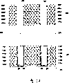
Can on substrate 10, form the alternating layer of organic and inorganic dielectric material by this way, as shown in Figure 5, up to the thickness of the first metal line level, 20 expectations.In this example, a layer 12c-12f comprises and is similar to the first and the 3rd insulating barrier 12a, the organic media material of 12b.Equally, a layer 14c-14f comprises and is similar to the second and the 4th insulating barrier 14a, the inorganic dielectric material of 14b.The number of the layer that illustrates in the present invention only is used for illustration purpose, and not intention restriction by any way, as long as have an organic layer and an inorganic layer at least.Equally, should be noted that at first depositing organic dielectric material in this example only is used for illustration purpose.Inorganic or organic media material can at first deposit.
Should be noted that equally and can deposit organic in position and alternating layer inorganic insulating material.For example, can use single PECVD chamber inorganic and organic two kinds of floor of deposition and not leave the chamber.Equally, can use rotation to apply track, wherein can and solidify alternating layer in identical indoor deposition.Use arbitrary technology, can deposit the first insulating barrier 12a alternatively with twice expectation thickness.Thereafter, the first insulating barrier 12a is exposed to plasma or heat treatment, wherein the upper part of the first insulating barrier 12a is converted into the material that needs among the second insulating barrier 14a.These methods can help to reduce the unbalanced of thickness between organic and the inorganic insulation layer, and can increase the adhesiveness between organic and the inorganic insulation layer.
As shown in Figure 6, behind the expectation thickness that reaches first wire level 20, in first wire level 20, form first parts 22 and second parts 24 in this example.First and second parts 22,24th, wire laying slot is used for the wiring that can use conventional composition and etching technique to form.
After first and second parts 22,24 form, select to be etched with and in first wire level 20, remove, in this example, in layer 12a-12f (Fig. 7) to small part organic media material.In this example, comprise p-SILK at the organic media material
TMComprise with inorganic dielectric material and can use N under the situation of p-OSG
2Plasma, H
2Plasma or other similar plasma etching are to select to remove the organic media material.Can in the pressure limit of about 3-200mT, under typical parallel-plate or high-density plasma power and current condition, carry out N
2Or H
2Etching.Alternatively, can use wet etchant etching inorganic dielectric material (p-OSG) part, in layer 14a-14f, stay SiLK as 100: 1 DHF
TMMaterial.
As shown in Figure 7, form opening or air gap 26 behind the organic media material in selecting etch layer 12a-12f.In the organic media material of layer 12a-12f rather than in the inorganic dielectric material of layer 14a-14f, form air gap 26, because the etch-rate of the organic media material of layer 12a-12f is faster than the etch-rate of the inorganic dielectric material of layer 14a-14f.Air gap 26 in first wire level 20 has reduced the electric capacity of entire device.Select to be etched with a part of removing the organic media material but the non-size of all coming to determine air gap 26 by calibration.After selecting etching, should keep at least some organic media materials collapsing with the mechanical breakdown that prevents device such as inorganic medium layer 14a-14f.
The table 1 that illustrates has compared roughly and has used different inorganic and organic materials below, has and do not have the capacitance of the device of air gap 26.More particularly, these data are that simulation has at interval about 100nm of the about 100nm of width of first wire level 20 and wiring, and wherein the sample that is removed of about 33nm of the organic media of the 100nm in the interval of connecting up obtains.Have an appointment in Keff (effective dielectric constant of device) 20% reduce of this result, this can be converted into the reducing of electric capacity about 20% of device, because the electric capacity of Keff and device is proportional.
Table 1: have the Keff of air gap and do not have the comparison of the Keff of air gap
| Inorganic medium | Organic media | Keff does not have air gap | Keff has air gap | The % of Keff reduces |
| SiO 2(K=4) | SiLK(K=2.6) | 3.30 | 2.70 | 18% |
| SiCOH(K=3) | SiLK(K=2.6) | 2.80 | 2.24 | 20% |
| p-SiCOH *(K=2.5) | SiLK(K=2.6) | 2.55 | 1.99 | 22% |
| p-SiO 2 *(K=2) | p-SiLK *(K=2.2) | 2.10 | 1.68 | 20% |
(
*" p-" expression medium is a porous media)
After forming air gap 26, the surface 28 that seals first metal wiring layer 20 leaks in the air gap 26 with the metal that prevents to deposit in next step.This can finish with several diverse ways.For example, deposition as have the medium of low-k on the surface 28 of first metal wiring layer 20, i.e. SiCOH, SiO
2, SiN, the conformal lining 30 (Fig. 8) of SiC and SiCN etc.Use PECVD, HDPCVD, SACVD, APCVD, THCVD, or the lining 30 of other similar techniques of deposition can have the thickness in about 1-10nm scope.
Alternatively, if air gap 26 is very little, for example, in the scope of about 1-10nm, the metal that deposits in later step can seal air gap 26 effectively.Can also use plasma gas phase deposition (PVD), chemical vapor deposition (CVD), ald (ALD), or other similar techniques of deposition metal is so that metal ion seldom infiltrates air gap 26.
Behind sealing air gap 26, if use sealing technology separately as described previously, deposited conductor material 32 is filled first and second parts 22,24 (Fig. 9) on the surface 28 of first wire level 20 so.Conductor material 32 can comprise copper, adds to be lined with thin clad lining hard to tolerate, as the material of technical known titanium or other similar application.Use routine techniques to polish the surface 28 of first wire level 20,, stay conductor material 32 in first and second parts 22,24 to form first wiring, 34 and second wiring, 36 (Figure 10) to remove unnecessary conductor material 32.
The first metal line level 20 that illustrates in this example is single mosaic wiring level.As shown in Figure 11-17, design the present invention is in order to be used in combination with the dual-damascene wiring level.As shown in Figure 11, deposition the 3rd insulating barrier 38 on the surface 28 of first wire level 20.The 3rd insulating barrier 38 can comprise one or more dielectric materials, has low-k, and it is difficult for removing in the etch process that is used to form air gap (below formation) subsequently.For example, the 3rd insulating barrier 38 can comprise porous SiC OH (p-OSG), SiO
2, fluoridize SiO
2(FSG), SiCOH (OSG) is as the porous form of methyl silsesquioxane (MSQ) or all these materials.The 3rd insulating barrier 38 can use CVD, PECVD, and spin-on deposition or other similar deposition technique form, and can comprise multilayer, as SiN, SiC, FSG etc.The 3rd insulating barrier 38 that forms can have the thickness that approximates final via height, as 0.1 to 1.0 micron.
The alternating layer of organic dielectric material 40a-40f of deposition and inorganic dielectric material 42a-42f on the surface 40 of the 3rd insulating barrier 38, as shown in figure 12, to form second wire level 50.Alternating layer with in the first metal line level 20, form similar (that is, and the organic media material, inorganic dielectric material, the organic media material, inorganic dielectric material, or the like), and form in a similar fashion.
After forming second wire level 50,, form the first dual damascene parts 44 in the alternating layer of inorganic dielectric material 42a-42f and the 3rd insulating barrier 38 at organic media material 40a-40f.As shown in figure 13, the first dual damascene parts 44 are via hole grooves.Use conventional composition and etching technique to form via hole groove 44 downwards up to the first metal line level 20.
As shown in Figure 14, at organic media material 40a-40f, form the second dual damascene parts 46 and second groove 48 in the alternating layer of inorganic dielectric material 42a-42f.The wire laying slot that the second dual damascene parts 46 are to use conventional composition and etching technique to form equally is down to the surface of the 3rd insulating barrier 38.Alternatively, as technical known, can use groove first via hole second technology.Equally, can use the hard mask of multilayer, wherein composition and etching first mosaic component in the hard mask in top are as technical known.
After forming the first and second dual damascene parts 44,46,48, select to be etched with remove in second wire level 50 to small part organic media material 40a-40f.As mentioned above, comprise p-SILK at the organic media material
TMComprise with inorganic dielectric material and can use N under the situation of p-OSG
2Plasma, H
2Plasma or other similar plasma etching are to select to remove the organic media material.Can in the pressure limit of about 3-200mT, under typical parallel-plate or high-density plasma power and current condition, carry out N
2Or H
2Etching.
As shown in figure 15, after selecting etching, in second wire level 50, form opening or air gap 52.Should be noted that and in the 3rd insulating barrier 38 of this example, do not form air gap 52 to increase mechanical strength and to make entire device stable.On the surface of second wire level 50, form conformal lining 53 then, seal second wire level 50 and leak in the air gap 52 with the metal that prevents to deposit in next step.
Deposited conductor material 54 on the surface of second wire level 50, filled vias groove 44 and groove 46,48 (Figure 16).Conductor material 54 can comprise copper, adds to be lined with thin clad lining hard to tolerate, as the material of technical known titanium or other similar application.Use routine techniques to polish the surface of second wire level 50,, stay conductor material 54 in via hole groove 44 and groove 46,48 to form conductor dual damascene parts 60 and conductor list mosaic component 62 (Figure 17) to remove unnecessary conductor material 54.
The formation of air gap has reduced the electric capacity of entire device in the metal line level in the present invention.This is more helpful when the distance between the more and more littler and device component reduces continuously at device.
Claims (30)
1. a method that forms semiconductor device comprises the steps:
Deposit the alternating layer of first and second dielectric materials, the rate selection etching that wherein said first and second dielectric materials can be different;
In the alternating layer of described dielectric material, form first parts; And
Select the alternating layer of the described dielectric material of etching, with in having every layer of described first dielectric material, remove described first dielectric material to small part but non-all, and stay the not etching basically of described second dielectric material.
2. according to the process of claim 1 wherein that described first dielectric material comprises that described second dielectric material is had optionally etched material.
3. according to the process of claim 1 wherein that described first dielectric material comprises that organic dielectric material and described second dielectric material comprise inorganic dielectric material.
4. according to the process of claim 1 wherein that described first dielectric material comprises organic dielectric material, is selected from: poly (arylene ether) (SILK
TM), Parylene (N), Parylene (F), polytetrafluoroethylene, porous poly (arylene ether) (SILK
TM), porous Parylene (N), porous Parylene (F) and porous Teflon, and wherein said second dielectric material comprises inorganic dielectric material, is selected from OSG, SiO
2, FSG, MSQ, porous OSG, porous SiO
2, porous FSG and porous MSQ.
5. according to the process of claim 1 wherein that described first parts comprise single mosaic component or dual damascene parts.
6. according to the method for claim 5, the part of not removing described first dielectric material wherein from the via hole trench portions of described dual damascene parts from the wire laying slot part of described dual damascene parts.
7. also comprise after the step of the alternating layer of the described dielectric material of described selection etching according to the process of claim 1 wherein:
Deposition conformal lining is to seal described alternating layer on the surface of the alternating layer of described dielectric material.
8. according to the method for claim 7, wherein said conformal lining comprises and is selected from SiCOH, SiO
2, SiN, the material of SiC and SiCN.
9. according to the method for claim 7, wherein after the step of described deposition conformal lining, also comprise:
Deposited conductor material layer on the surface of described device is filled described first parts; And
Polish the described surface of described device,, stay the described conductor material in described first parts to remove described lip-deep unnecessary conductor material at described device.
10. a method that forms semiconductor device comprises the steps:
Deposit the alternating layer of first and second insulating material;
In the alternating layer of described first and second insulating material, form first parts; And
In described first insulation material layer, form opening.
11. according to the method for claim 10, wherein said first insulating material comprises that described second insulating material is had optionally etched material.
12. according to the method for claim 10, wherein said first insulating material comprises organic dielectric material, is selected from: poly (arylene ether) (SILK
TM), Parylene (N), Parylene (F), polytetrafluoroethylene, porous poly (arylene ether) (SILK
TM), porous Parylene (N), porous Parylene (F) and porous Teflon, and wherein said second insulating material comprises inorganic dielectric material, is selected from OSG, SiO
2, FSG, MSQ, porous OSG, porous SiO
2, porous FSG and porous MSQ.
13. according to the method for claim 10, wherein said first parts comprise single mosaic component or dual damascene parts.
14., wherein partly do not remove described first insulating material from the via hole trench portions from the wire laying slot of described dual damascene parts according to the method for claim 13.
15., wherein after the described step that in described first insulation material layer, forms opening, also comprise according to the method for claim 10:
Deposition conformal lining to be sealing described alternating layer on the surface of the alternating layer of dielectric material, and wherein said conformal lining comprises and is selected from SiCOH, SiO
2, SiN, the material of SiC and SiCN.
16. a semiconductor device comprises:
The metal line level has the alternating layer of first dielectric material and second dielectric material and have first parts that form in the alternating layer of first and second dielectric materials; And
A plurality of openings in described first dielectric material.
17. according to the semiconductor device of claim 16, wherein said first dielectric material comprises that described second dielectric material is had optionally etched material.
18. according to the semiconductor device of claim 16, wherein said first dielectric material comprises organic dielectric material, is selected from: poly (arylene ether) (SILK
TM), Parylene (N), Parylene (F), polytetrafluoroethylene, porous poly (arylene ether) (SILK
TM), porous Parylene (N), porous Parylene (F) and porous Teflon, and wherein said second dielectric material comprises inorganic dielectric material, is selected from OSG, SiO
2, FSG, MSQ, porous OSG, porous SiO
2, porous FSG and porous MSQ.
19., wherein partly do not remove described first dielectric material from the via hole trench portions from the wire laying slot of described dual damascene parts according to the semiconductor device of claim 18.
20. the semiconductor device according to claim 16 also comprises:
With the sealing alternating layer, wherein said conformal lining comprises and is selected from SiCOH, SiO at the lip-deep conformal lining of the alternating layer of dielectric material
2, SiN, the material of SiC and SiCN.
21. the semiconductor device according to claim 16 also comprises:
Conductor material in described first parts.
22. the semiconductor device according to claim 16 also comprises:
The second metal line level has the alternating layer of first dielectric material and second dielectric material, forms on described metal line level, has opening in described first dielectric material of the described second metal line level;
Second parts form in the described alternating layer of first and second dielectric materials of the described second metal line level; And
A plurality of openings are in described first dielectric material of the described second metal line level.
23. a semiconductor device comprises:
A plurality of first and second insulating barriers that replace, wherein said first and second insulating barriers have different etch-rates;
First parts form in described first and second insulating barriers;
A plurality of openings in a plurality of first insulating barriers, form during the selection etching.
24. according to the semiconductor device of claim 23, wherein said first insulating barrier comprises that described second insulating barrier is had optionally etched material.
25. according to the semiconductor device of claim 23, wherein said first insulating barrier comprises that organic dielectric material and described second insulating barrier comprise inorganic dielectric material.
26. according to the semiconductor device of claim 23, wherein said first insulating barrier comprises organic dielectric material, is selected from: poly (arylene ether) (SILK
TM), Parylene (N), Parylene (F), polytetrafluoroethylene, porous poly (arylene ether) (SILK
TM), porous Parylene (N), porous Parylene (F) and porous Teflon, and wherein said second insulating barrier comprises inorganic dielectric material, is selected from OSG, SiO
2, FSG, MSQ, porous OSG, porous SiO
2, porous FSG and porous MSQ.
27. according to the semiconductor device of claim 23, wherein said first parts comprise single mosaic component or dual damascene parts.
28. according to the semiconductor device of claim 27, wherein said opening is not in the wire laying slot part of described dual damascene parts and in the via hole trench portions.
29. the semiconductor device according to claim 23 also comprises:
With the sealing alternating layer, wherein said conformal lining comprises and is selected from SiCOH, SiO at the lip-deep conformal lining of the alternating layer of dielectric material
2, SiN, the material of SiC and SiCN.
30. the semiconductor device according to claim 23 also comprises:
Conductor material in described first parts.
Applications Claiming Priority (2)
| Application Number | Priority Date | Filing Date | Title |
|---|---|---|---|
| US10/709,722 US7078814B2 (en) | 2004-05-25 | 2004-05-25 | Method of forming a semiconductor device having air gaps and the structure so formed |
| US10/709,722 | 2004-05-25 |
Publications (1)
| Publication Number | Publication Date |
|---|---|
| CN1954414A true CN1954414A (en) | 2007-04-25 |
Family
ID=35451549
Family Applications (1)
| Application Number | Title | Priority Date | Filing Date |
|---|---|---|---|
| CNA2005800153631A Pending CN1954414A (en) | 2004-05-25 | 2005-05-23 | Gap type conductive interconnecting structure in semiconductor device |
Country Status (7)
| Country | Link |
|---|---|
| US (3) | US7078814B2 (en) |
| EP (1) | EP1766670A4 (en) |
| JP (1) | JP5362985B2 (en) |
| KR (1) | KR100956718B1 (en) |
| CN (1) | CN1954414A (en) |
| TW (1) | TW200539382A (en) |
| WO (1) | WO2005117085A2 (en) |
Cited By (1)
| Publication number | Priority date | Publication date | Assignee | Title |
|---|---|---|---|---|
| CN101645453B (en) * | 2008-08-06 | 2011-07-27 | 株式会社日立制作所 | Nonvolatile memory device and method of manufacturing the same |
Families Citing this family (26)
| Publication number | Priority date | Publication date | Assignee | Title |
|---|---|---|---|---|
| US6291298B1 (en) * | 1999-05-25 | 2001-09-18 | Advanced Analogic Technologies, Inc. | Process of manufacturing Trench gate semiconductor device having gate oxide layer with multiple thicknesses |
| US7229499B2 (en) * | 2003-08-22 | 2007-06-12 | Matsushita Electric Industrial Co., Ltd. | Manufacturing method for semiconductor device, semiconductor device and semiconductor wafer |
| US7071091B2 (en) * | 2004-04-20 | 2006-07-04 | Intel Corporation | Method of forming air gaps in a dielectric material using a sacrificial film |
| US7629225B2 (en) * | 2005-06-13 | 2009-12-08 | Infineon Technologies Ag | Methods of manufacturing semiconductor devices and structures thereof |
| US7732322B2 (en) * | 2006-02-23 | 2010-06-08 | International Business Machines Corporation | Dielectric material with reduced dielectric constant and methods of manufacturing the same |
| JP4827639B2 (en) * | 2006-07-12 | 2011-11-30 | ルネサスエレクトロニクス株式会社 | Semiconductor device and manufacturing method thereof |
| US7482261B2 (en) * | 2006-07-26 | 2009-01-27 | International Business Machines Corporation | Interconnect structure for BEOL applications |
| TWI321819B (en) * | 2006-11-27 | 2010-03-11 | Innolux Display Corp | Metal line damascene structure and fabricating method for the same |
| US7485567B2 (en) * | 2007-02-02 | 2009-02-03 | International Business Machines Corporation | Microelectronic circuit structure with layered low dielectric constant regions and method of forming same |
| US20080185722A1 (en) * | 2007-02-05 | 2008-08-07 | Chung-Shi Liu | Formation process of interconnect structures with air-gaps and sidewall spacers |
| JP2008205283A (en) * | 2007-02-21 | 2008-09-04 | Matsushita Electric Ind Co Ltd | Wiring structure for semiconductor integrated circuit device, designing method and designing apparatus thereof |
| US7544602B2 (en) * | 2007-03-29 | 2009-06-09 | International Business Machines Corporation | Method and structure for ultra narrow crack stop for multilevel semiconductor device |
| US8138036B2 (en) | 2008-08-08 | 2012-03-20 | International Business Machines Corporation | Through silicon via and method of fabricating same |
| US8298911B2 (en) * | 2009-03-26 | 2012-10-30 | Samsung Electronics Co., Ltd. | Methods of forming wiring structures |
| KR101536333B1 (en) * | 2009-03-26 | 2015-07-14 | 삼성전자주식회사 | Wiring structure and Method of forming the same |
| WO2011021244A1 (en) * | 2009-08-20 | 2011-02-24 | 富士通セミコンダクター株式会社 | Semiconductor device manufacturing method |
| US8003516B2 (en) * | 2009-08-26 | 2011-08-23 | International Business Machines Corporation | BEOL interconnect structures and related fabrication methods |
| US8456009B2 (en) * | 2010-02-18 | 2013-06-04 | Taiwan Semiconductor Manufacturing Company, Ltd. | Semiconductor structure having an air-gap region and a method of manufacturing the same |
| KR20120048991A (en) * | 2010-11-08 | 2012-05-16 | 삼성전자주식회사 | Semiconductor devices and methods of fabricating the same |
| CN103021929A (en) * | 2011-09-22 | 2013-04-03 | 中芯国际集成电路制造(北京)有限公司 | Manufacturing method of semiconductor device |
| KR101827893B1 (en) | 2012-02-22 | 2018-02-09 | 삼성전자주식회사 | Wiring line structure and method of forming the same |
| US8900989B2 (en) | 2013-03-06 | 2014-12-02 | Taiwan Semiconductor Manufacturing Company, Ltd. | Method of fabricating an air gap using a damascene process and structure of same |
| EP3796371A3 (en) * | 2013-09-27 | 2021-10-06 | INTEL Corporation | Self-aligned via and plug patterning for back end of line (beol) interconnects |
| US9853025B1 (en) * | 2016-10-14 | 2017-12-26 | International Business Machines Corporation | Thin film metallic resistors formed by surface treatment of insulating layer |
| US11004612B2 (en) * | 2019-03-14 | 2021-05-11 | MicroSol Technologies Inc. | Low temperature sub-nanometer periodic stack dielectrics |
| US20220115239A1 (en) * | 2020-04-10 | 2022-04-14 | Hitachi High-Tech Corporation | Etching method |
Family Cites Families (32)
| Publication number | Priority date | Publication date | Assignee | Title |
|---|---|---|---|---|
| JPH05283542A (en) | 1992-03-31 | 1993-10-29 | Mitsubishi Electric Corp | Semiconductor integrated circuit device and manufacture thereof |
| US5470801A (en) | 1993-06-28 | 1995-11-28 | Lsi Logic Corporation | Low dielectric constant insulation layer for integrated circuit structure and method of making same |
| US5461003A (en) | 1994-05-27 | 1995-10-24 | Texas Instruments Incorporated | Multilevel interconnect structure with air gaps formed between metal leads |
| US5548159A (en) | 1994-05-27 | 1996-08-20 | Texas Instruments Incorporated | Porous insulator for line-to-line capacitance reduction |
| KR100440418B1 (en) * | 1995-12-12 | 2004-10-20 | 텍사스 인스트루먼츠 인코포레이티드 | Low pressure, low temperature semiconductor gap filling treatment |
| US5994776A (en) | 1996-01-11 | 1999-11-30 | Advanced Micro Devices, Inc. | Interlevel dielectric with multiple air gaps between conductive lines of an integrated circuit |
| US5965202A (en) | 1996-05-02 | 1999-10-12 | Lucent Technologies, Inc. | Hybrid inorganic-organic composite for use as an interlayer dielectric |
| WO2004074355A1 (en) | 1997-05-28 | 2004-09-02 | Noriko Yamada | Low-permittivity material, and production and use thereof |
| US6577011B1 (en) | 1997-07-10 | 2003-06-10 | International Business Machines Corporation | Chip interconnect wiring structure with low dielectric constant insulator and methods for fabricating the same |
| JP3571522B2 (en) | 1998-02-12 | 2004-09-29 | 松下電器産業株式会社 | Method for forming porous film and material for forming porous film |
| US6479374B1 (en) | 1998-04-01 | 2002-11-12 | Asahi Kasei Kabushiki Kaisha | Method of manufacturing interconnection structural body |
| US6265780B1 (en) | 1998-12-01 | 2001-07-24 | United Microelectronics Corp. | Dual damascene structure for the wiring-line structures of multi-level interconnects in integrated circuit |
| US6245662B1 (en) * | 1998-07-23 | 2001-06-12 | Applied Materials, Inc. | Method of producing an interconnect structure for an integrated circuit |
| JP3888794B2 (en) | 1999-01-27 | 2007-03-07 | 松下電器産業株式会社 | Method for forming porous film, wiring structure and method for forming the same |
| US6177329B1 (en) * | 1999-04-15 | 2001-01-23 | Kurt Pang | Integrated circuit structures having gas pockets and method for forming integrated circuit structures having gas pockets |
| US6090698A (en) * | 1999-07-23 | 2000-07-18 | United Microelectronics Corp | Fabrication method for an insulation structure having a low dielectric constant |
| US6596624B1 (en) | 1999-07-31 | 2003-07-22 | International Business Machines Corporation | Process for making low dielectric constant hollow chip structures by removing sacrificial dielectric material after the chip is joined to a chip carrier |
| US6103619A (en) * | 1999-10-08 | 2000-08-15 | United Microelectronics Corp. | Method of forming a dual damascene structure on a semiconductor wafer |
| JP2001118842A (en) * | 1999-10-15 | 2001-04-27 | Nec Corp | Semiconductor device and its manufacturing method |
| US6815329B2 (en) * | 2000-02-08 | 2004-11-09 | International Business Machines Corporation | Multilayer interconnect structure containing air gaps and method for making |
| US6297554B1 (en) * | 2000-03-10 | 2001-10-02 | United Microelectronics Corp. | Dual damascene interconnect structure with reduced parasitic capacitance |
| US6362091B1 (en) | 2000-03-14 | 2002-03-26 | Intel Corporation | Method for making a semiconductor device having a low-k dielectric layer |
| US6265321B1 (en) * | 2000-04-17 | 2001-07-24 | Chartered Semiconductor Manufacturing Ltd. | Air bridge process for forming air gaps |
| US6287979B1 (en) | 2000-04-17 | 2001-09-11 | Chartered Semiconductor Manufacturing Ltd. | Method for forming an air gap as low dielectric constant material using buckminsterfullerene as a porogen in an air bridge or a sacrificial layer |
| US6413852B1 (en) | 2000-08-31 | 2002-07-02 | International Business Machines Corporation | Method of forming multilevel interconnect structure containing air gaps including utilizing both sacrificial and placeholder material |
| KR100841597B1 (en) | 2000-09-13 | 2008-06-26 | 롬 앤드 하스 일렉트로닉 머트어리얼즈, 엘.엘.씨 | Electronic device manufacture |
| TW465039B (en) * | 2000-11-06 | 2001-11-21 | United Microelectronics Corp | Void-type metal interconnect and method for making the same |
| US6603204B2 (en) | 2001-02-28 | 2003-08-05 | International Business Machines Corporation | Low-k interconnect structure comprised of a multilayer of spin-on porous dielectrics |
| US6448177B1 (en) * | 2001-03-27 | 2002-09-10 | Intle Corporation | Method of making a semiconductor device having a dual damascene interconnect spaced from a support structure |
| US6933586B2 (en) | 2001-12-13 | 2005-08-23 | International Business Machines Corporation | Porous low-k dielectric interconnects with improved adhesion produced by partial burnout of surface porogens |
| JP2003289099A (en) * | 2002-03-27 | 2003-10-10 | Toshiba Corp | Semiconductor device and its manufacturing method |
| FR2851373B1 (en) * | 2003-02-18 | 2006-01-13 | St Microelectronics Sa | METHOD FOR MANUFACTURING AN INTEGRATED ELECTRONIC CIRCUIT INCORPORATING CAVITIES |
-
2004
- 2004-05-25 US US10/709,722 patent/US7078814B2/en active Active
-
2005
- 2005-05-04 TW TW094114443A patent/TW200539382A/en unknown
- 2005-05-23 KR KR1020067022307A patent/KR100956718B1/en not_active IP Right Cessation
- 2005-05-23 EP EP05751777A patent/EP1766670A4/en not_active Withdrawn
- 2005-05-23 JP JP2007515228A patent/JP5362985B2/en not_active Expired - Fee Related
- 2005-05-23 WO PCT/US2005/018050 patent/WO2005117085A2/en active Application Filing
- 2005-05-23 CN CNA2005800153631A patent/CN1954414A/en active Pending
-
2006
- 2006-03-28 US US11/391,050 patent/US7459389B2/en not_active Expired - Fee Related
-
2008
- 2008-08-29 US US12/201,266 patent/US7674705B2/en not_active Expired - Fee Related
Cited By (1)
| Publication number | Priority date | Publication date | Assignee | Title |
|---|---|---|---|---|
| CN101645453B (en) * | 2008-08-06 | 2011-07-27 | 株式会社日立制作所 | Nonvolatile memory device and method of manufacturing the same |
Also Published As
| Publication number | Publication date |
|---|---|
| US20050275104A1 (en) | 2005-12-15 |
| JP2008502140A (en) | 2008-01-24 |
| KR20070021191A (en) | 2007-02-22 |
| US7674705B2 (en) | 2010-03-09 |
| WO2005117085A3 (en) | 2006-10-12 |
| US7078814B2 (en) | 2006-07-18 |
| TW200539382A (en) | 2005-12-01 |
| US20090008788A1 (en) | 2009-01-08 |
| US7459389B2 (en) | 2008-12-02 |
| JP5362985B2 (en) | 2013-12-11 |
| WO2005117085A2 (en) | 2005-12-08 |
| EP1766670A2 (en) | 2007-03-28 |
| EP1766670A4 (en) | 2011-03-02 |
| KR100956718B1 (en) | 2010-05-06 |
| US20060166486A1 (en) | 2006-07-27 |
Similar Documents
| Publication | Publication Date | Title |
|---|---|---|
| CN1954414A (en) | Gap type conductive interconnecting structure in semiconductor device | |
| US5792706A (en) | Interlevel dielectric with air gaps to reduce permitivity | |
| US7037851B2 (en) | Methods for selective integration of airgaps and devices made by such methods | |
| US6043145A (en) | Method for making multilayer wiring structure | |
| US6211561B1 (en) | Interconnect structure and method employing air gaps between metal lines and between metal layers | |
| US20040232552A1 (en) | Air gap dual damascene process and structure | |
| CN100541760C (en) | The cross direction profiles control of the air gap in the interconnection | |
| US20060019485A1 (en) | Multi-layer wiring structure, semiconductor apparatus having multi-layer wiring structure, and methods of manufacturing them | |
| KR100307490B1 (en) | Method for reducing prostitute capacitance | |
| US20070120263A1 (en) | Conductor track arrangement and associated production method | |
| CN100405574C (en) | Dual damascene interconnect structures having different materials for line and via conductors | |
| US7056826B2 (en) | Method of forming copper interconnects | |
| KR100706380B1 (en) | Lithographic method for creating damascene metallization layers | |
| US20020145201A1 (en) | Method and apparatus for making air gap insulation for semiconductor devices | |
| US7510959B2 (en) | Method of manufacturing a semiconductor device having damascene structures with air gaps | |
| US8421239B2 (en) | Crenulated wiring structure and method for integrated circuit interconnects | |
| EP1378935A2 (en) | A method to form both high and low-K materials in one plane on a substrate, and their application in mixed mode circuits | |
| CN1103496C (en) | Method of forming shielding wire adjacement to signal wire | |
| CN104851835A (en) | Metal interconnection structure and forming method thereof | |
| CN103904024B (en) | The method forming the dual-damascene structure of semiconductor devices and the semiconductor devices being produced from | |
| CN102044471B (en) | Interconnecting structure and forming method thereof | |
| JP2005129937A (en) | Low k integrated circuit interconnection structure | |
| EP1577940B1 (en) | Method of manufacturing a semiconductor device having damascene structures with air gaps | |
| KR100641498B1 (en) | Method for manufacturing metal line with dual damascene structure | |
| CN105226005A (en) | The formation method of dual-damascene structure |
Legal Events
| Date | Code | Title | Description |
|---|---|---|---|
| C06 | Publication | ||
| PB01 | Publication | ||
| C10 | Entry into substantive examination | ||
| SE01 | Entry into force of request for substantive examination | ||
| C12 | Rejection of a patent application after its publication | ||
| RJ01 | Rejection of invention patent application after publication |