JP5361258B2 - Image forming apparatus and image forming apparatus control method - Google Patents
Image forming apparatus and image forming apparatus control method Download PDFInfo
- Publication number
- JP5361258B2 JP5361258B2 JP2008157860A JP2008157860A JP5361258B2 JP 5361258 B2 JP5361258 B2 JP 5361258B2 JP 2008157860 A JP2008157860 A JP 2008157860A JP 2008157860 A JP2008157860 A JP 2008157860A JP 5361258 B2 JP5361258 B2 JP 5361258B2
- Authority
- JP
- Japan
- Prior art keywords
- image
- voltage
- carrier
- developer
- developing
- Prior art date
- Legal status (The legal status is an assumption and is not a legal conclusion. Google has not performed a legal analysis and makes no representation as to the accuracy of the status listed.)
- Expired - Fee Related
Links
Images


Classifications
-
- G—PHYSICS
- G03—PHOTOGRAPHY; CINEMATOGRAPHY; ANALOGOUS TECHNIQUES USING WAVES OTHER THAN OPTICAL WAVES; ELECTROGRAPHY; HOLOGRAPHY
- G03G—ELECTROGRAPHY; ELECTROPHOTOGRAPHY; MAGNETOGRAPHY
- G03G15/00—Apparatus for electrographic processes using a charge pattern
- G03G15/06—Apparatus for electrographic processes using a charge pattern for developing
- G03G15/065—Arrangements for controlling the potential of the developing electrode
-
- G—PHYSICS
- G03—PHOTOGRAPHY; CINEMATOGRAPHY; ANALOGOUS TECHNIQUES USING WAVES OTHER THAN OPTICAL WAVES; ELECTROGRAPHY; HOLOGRAPHY
- G03G—ELECTROGRAPHY; ELECTROPHOTOGRAPHY; MAGNETOGRAPHY
- G03G2215/00—Apparatus for electrophotographic processes
- G03G2215/06—Developing structures, details
- G03G2215/0634—Developing device
Abstract
Description
本発明は、現像により画像を形成する画像形成装置及び画像形成装置の制御方法に関する。 The present invention relates to an image forming apparatus that forms an image by development and a method for controlling the image forming apparatus .
従来、電子写真方式で画像形成を行う画像形成装置や静電記録方式で画像形成を行う画像形成装置では、静電潜像を担持した像担持体(感光ドラム)に、現像剤を担持した現像器の現像剤担持体(現像スリーブ)を対応させて現像を行うことが一般的である。現像を行う際は、感光ドラムと現像スリーブの間に現像電界を形成するために、現像スリーブに現像バイアス電圧を印加する。 2. Description of the Related Art Conventionally, in an image forming apparatus that forms an image using an electrophotographic method or an image forming apparatus that forms an image using an electrostatic recording method, development with a developer carried on an image carrier (photosensitive drum) carrying an electrostatic latent image. In general, development is performed in correspondence with the developer carrier (developing sleeve) of the container. When developing, a developing bias voltage is applied to the developing sleeve in order to form a developing electric field between the photosensitive drum and the developing sleeve.
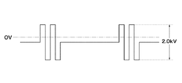
現像バイアス電圧としては、例えば図18に示すようにDC(直流)成分にAC(交流)成分を重畳した現像バイアス電圧が用いられている。即ち、図18に示す現像バイアス電圧(本明細書では矩形バイアス電圧と称する)のAC成分の矩形波としては、従来、周波数が2kHz(1/2周期=250μ秒)程度、ピークツーピーク電圧(Vp−p)が2kV程度のものが用いられている。 As the developing bias voltage, for example, as shown in FIG. 18, a developing bias voltage in which an AC (alternating current) component is superimposed on a DC (direct current) component is used. That is, as a rectangular wave of the AC component of the developing bias voltage (referred to as a rectangular bias voltage in this specification) shown in FIG. 18, conventionally, the frequency is about 2 kHz (1/2 period = 250 μsec), and the peak-to-peak voltage ( Vp-p) of about 2 kV is used.
また、トナーとキャリアからなる2成分現像剤を用いた現像(2成分現像)に関しては、図19に示すようにDC成分にAC成分を断続的に重畳した現像バイアス電圧を用いる技術が提案されている。図19に示す現像バイアス電圧(本明細書ではブランクパルスバイアス電圧(BPバイアス電圧)と称する)は、パルス部と休止部(ブランク部)から構成されている。 As for development using a two-component developer composed of a toner and a carrier (two-component development), a technique using a development bias voltage in which an AC component is intermittently superimposed on a DC component is proposed as shown in FIG. Yes. The developing bias voltage (referred to as a blank pulse bias voltage (BP bias voltage) in this specification) shown in FIG. 19 includes a pulse portion and a pause portion (blank portion).
現像バイアス電圧のAC成分であるACバイアス電圧の波形に関する技術については各種の技術が提案されている(例えば、特許文献1、特許文献2、特許文献3参照)。尚、各特許文献では、画像形成装置の感光ドラムと現像スリーブの間に設けられる所定のギャップ(S−Dギャップ)のばらつきに対する対策については開示されていない。
しかしながら、従来技術においては以下のような問題がある。 However, the prior art has the following problems.
図19の現像バイアス電圧を用いた場合は、図18の現像バイアス電圧を用いた場合に比べて現像性が良いが、現像で得られた画像のハイライト部のがさつきをなくすためには現像バイアス電圧のパルス部の周波数を4kHz以上に上げることが必要である。また、画像の濃度を出す条件として、現像バイアス電圧のパルス部のVp−pを矩形バイアス電圧と同様に約2kV以上に設定することが必要である。図18、図19のようにDC成分に重畳したAC成分(ACバイアス電圧)は現像性の向上に役立っているが、ACバイアス電圧が過大であると、現像器の内部に異物が混入した際にリングマークが発生する等の画像不良を生ずる。 When the development bias voltage of FIG. 19 is used, developability is better than when the development bias voltage of FIG. 18 is used. However, in order to eliminate the roughness of the highlight portion of the image obtained by development, development is performed. It is necessary to increase the frequency of the pulse part of the bias voltage to 4 kHz or more. Further, as a condition for obtaining the image density, it is necessary to set Vp-p of the pulse portion of the developing bias voltage to about 2 kV or more like the rectangular bias voltage. As shown in FIGS. 18 and 19, the AC component (AC bias voltage) superimposed on the DC component is useful for improving the developability. However, if the AC bias voltage is excessive, foreign matter is mixed inside the developing device. This causes image defects such as ring marks.
一方、画像形成装置では感光ドラムと現像スリーブの間に所定のギャップ(以下S−Dギャップと表記)を設けている。S−Dギャップを維持するため、現像スリーブの端部に設けた突き当てコロを感光ドラムの表面に突き当てる構成、もしくは現像スリーブの回転軸と感光ドラムの回転軸の間にスペーサを固定する構成をとっている。S−Dギャップが狭いと現像性は向上するものの、上述したACバイアス電圧が過大な時のように画像不良が生じる。また、S−Dギャップが広いと現像性が低下する。 On the other hand, in the image forming apparatus, a predetermined gap (hereinafter referred to as SD gap) is provided between the photosensitive drum and the developing sleeve. In order to maintain the SD gap, a configuration in which an abutting roller provided at an end of the developing sleeve is abutted against the surface of the photosensitive drum, or a configuration in which a spacer is fixed between the rotating shaft of the developing sleeve and the rotating shaft of the photosensitive drum Have taken. When the SD gap is narrow, developability is improved, but an image defect occurs as in the case where the AC bias voltage is excessive. In addition, when the SD gap is wide, developability deteriorates.
しかし、突き当てコロの径のばらつきやスペーサの寸法のばらつき等により、S−Dギャップは画像形成装置毎にばらつくという問題がある。元々、設計上の中心値である、S−Dギャップの称呼値は、例えば300umといった非常に狭いものであるため、部品の公差等によるばらつきにより±20%程度変わる場合がある。S−Dギャップが狭い側にばらついて300umの称呼値に対して例えば240umになった場合、高電圧(以下高圧)の現像バイアス電圧が狭くなったS−Dギャップに印加される結果、S−Dギャップの電界は非常に大きなものになる。 However, there is a problem that the SD gap varies from one image forming apparatus to another due to variations in the diameter of the abutting rollers and variations in the dimensions of the spacers. Originally, the nominal value of the SD gap, which is the design center value, is very narrow, for example, 300 μm, and may vary by about ± 20% due to variations due to component tolerances. When the SD gap varies to the narrow side and reaches a nominal value of 300 μm, for example, 240 μm, a high-voltage (hereinafter high-voltage) developing bias voltage is applied to the narrowed SD gap. The electric field in the D gap is very large.
また、現像器の内部に導電性の異物が混入した場合、現像スリーブにおける感光ドラムと対向する側の導電性の異物が存在する部分では更にS−Dギャップが狭くなり、その部分で異常放電が発生する。その結果、画像にリング状の斑点が形成され著しく画像品位を落とすという問題が発生する。また、逆にS−Dギャップが広くなった場合、上述したように現像性が低下するという問題が発生する。 Further, when conductive foreign matter is mixed inside the developing device, the SD gap is further narrowed in the portion where the conductive foreign matter on the side facing the photosensitive drum in the developing sleeve is present, and abnormal discharge occurs in that portion. Occur. As a result, a ring-shaped spot is formed on the image, which causes a problem that the image quality is remarkably deteriorated. On the other hand, when the SD gap is widened, there arises a problem that developability deteriorates as described above.
他方、磁性体を含むトナーからなる1成分現像剤を用いた1成分ジャンピング現像では、現像スリーブと感光ドラムの間の電界により現像剤が飛翔する現象を利用して現像を行う。1成分ジャンピング現像では、S−Dギャップが広いか狭いかに応じて画像の濃度が変わるという問題がある。この場合、1成分ジャンピング現像では、矩形波のAC成分とDC成分を重畳した現像バイアス電圧が主に用いられる。現像を行う際は、現像スリーブの現像剤の穂が感光ドラムに接触せず、感光ドラムの潜像を形成するための電位と現像スリーブの電位との間の電位差によって生じた電界により、現像剤を飛翔させて現像を行う。 On the other hand, in one-component jumping development using a one-component developer made of toner containing a magnetic material, development is performed using a phenomenon in which the developer flies by an electric field between the developing sleeve and the photosensitive drum. In the one-component jumping development, there is a problem that the image density changes depending on whether the SD gap is wide or narrow. In this case, in the one-component jumping development, a development bias voltage in which a rectangular wave AC component and a DC component are superimposed is mainly used. During development, the developer sleeve on the developing sleeve does not contact the photosensitive drum, and the developer is generated by an electric field generated by a potential difference between the potential for forming the latent image on the photosensitive drum and the potential of the developing sleeve. Develop by flying.
しかし、1成分ジャンピング現像では、S−Dギャップの広さにより電界が異なる結果、画像の濃度まで変化するという問題がある。そのため、S−Dギャップの動的変動があると、S−Dギャップの広いところでは画像濃度が薄く、S−Dギャップの狭いところでは画像濃度が濃くなり、画像に帯状の濃淡が発生するという問題がある。 However, in the one-component jumping development, there is a problem that the electric field varies depending on the width of the SD gap, and as a result, the density of the image changes. Therefore, if there is a dynamic variation of the SD gap, the image density is low where the SD gap is wide, the image density is high where the SD gap is narrow, and band-like shading occurs in the image. There's a problem.
本発明の目的は、現像性を向上させた上で、画像不良の発生を抑制すると共に画像濃度を一定に保つことを可能とした画像形成装置及び画像形成装置の制御方法を提供することにある。 SUMMARY OF THE INVENTION An object of the present invention is to provide an image forming apparatus and an image forming apparatus control method capable of suppressing the occurrence of image defects and keeping the image density constant while improving developability. .
上述の目的を達成するために、本発明に係る画像形成装置は、静電潜像を担持する像担持体と、前記像担持体に対向して配置され前記像担持体に担持された静電潜像の現像に用いる現像剤を担持する現像剤担持体とを備え、前記静電潜像を前記現像剤を用いて現像することで画像形成を行う画像形成装置において、前記像担持体と前記現像剤担持体の間に現像電界を形成するための現像バイアス電圧を前記現像剤担持体に印加する印加手段と、前記像担持体と前記現像剤担持体の間の容量を検出する検出手段と、前記像担持体が回転している間に前記検出手段により検出された容量に従って、前記像担持体の外周の複数個所における前記像担持体と前記現像剤担持体との間のギャップについてのプロファイルであって、前記現像剤担持体の偏芯成分を除去したプロファイルを、画像形成動作に先立って作成する作成手段と、前記作成手段により作成された前記現像剤担持体の偏芯成分を除去したプロファイルに基づいて、前記像担持体と前記現像剤担持体との間のギャップの変動が画像に及ぼす影響を解消するように、画像形成を行う条件を変更する制御手段と、を備えることを特徴とする。 In order to achieve the above-described object, an image forming apparatus according to the present invention includes an image carrier that carries an electrostatic latent image, and an electrostatic that is disposed opposite to the image carrier and is carried on the image carrier. In an image forming apparatus comprising: a developer carrying member that carries a developer used for developing a latent image; and performing image formation by developing the electrostatic latent image using the developer. An applying means for applying a developing bias voltage for forming a developing electric field between the developer carrying bodies to the developer carrying body, and a detecting means for detecting a capacity between the image carrying body and the developer carrying body. The profile of the gap between the image carrier and the developer carrier at a plurality of locations on the outer periphery of the image carrier according to the capacity detected by the detection means while the image carrier is rotating The bias of the developer carrying member The profile obtained by removing the component, and creating means for creating, prior to the image forming operation, based on the profile obtained by removing the eccentricity component of the created the developer carrier by said forming means, the developing and the image bearing member Control means for changing the conditions for image formation so as to eliminate the influence of the fluctuation of the gap with the agent carrier on the image.
本発明によれば、像担持体と現像剤担持体の間の検出した容量に基づいて、画像形成を行う条件を変更するので、像担持体と現像剤担持体の間の間隔のばらつきに対応することが可能となる。これにより、現像性を向上させた上で、画像不良の発生を抑制することが可能となると共に画像濃度を一定に保つことが可能となる。 According to the present invention, since the conditions for image formation are changed based on the detected capacity between the image carrier and the developer carrier, it is possible to cope with variations in the distance between the image carrier and the developer carrier. It becomes possible to do. As a result, it is possible to improve the developability, suppress the occurrence of image defects, and keep the image density constant.
以下、本発明の実施の形態を図面に基づいて説明する。 Hereinafter, embodiments of the present invention will be described with reference to the drawings.
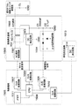
〔第1の実施の形態〕
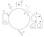
図1は、本発明の第1の実施の形態に係る画像形成装置の感光ドラムと現像器を中心とした構成を示す構成図である。
[First Embodiment]
FIG. 1 is a configuration diagram showing a configuration centering on a photosensitive drum and a developing unit of an image forming apparatus according to a first embodiment of the present invention.
図1において、画像形成装置は、感光ドラム1の周囲に、一次帯電器2、現像器4、転写帯電器5、クリーニング部6、前露光部11を配置した構造を有する。画像形成装置は、感光ドラム1に形成した静電潜像を現像したトナー像を用紙に転写する電子写真方式の画像形成を行う。感光ドラム1は、静電潜像を担持する像担持体であり、駆動機構(不図示)により矢印R方向に回転駆動される。帯電工程では、感光ドラム1の表面は一次帯電器2により均一に帯電される。露光工程では、形成対象の画像に応じたレーザ光Lがレーザ駆動部(不図示)により感光ドラム1の表面に露光され、静電潜像が形成される。
In FIG. 1, the image forming apparatus has a structure in which a
現像器4は、現像スリーブ4a、現像スクリュー4b、現像スクリュー4cを備えると共に、トナーとキャリアとからなる2成分現像剤を収容しており、感光ドラム表面の静電潜像の現像を行う。現像スリーブ4aは、現像剤を担持する現像剤担持体であり、感光ドラム1に対向して配置される。現像工程では、感光ドラム1と現像スリーブ4aの間に現像電界を形成するために、現像高圧基板(図3参照)から現像スリーブ4aに現像バイアスを印加する。これに伴い、感光ドラム1の表面に形成された静電潜像は、現像器4により現像されトナー像として可視化される。本実施の形態では、トナーはマイナス極性に帯電されている。
The developing
転写工程では、紙搬送機構(不図示)により搬送されてくる用紙に感光ドラム上のトナー像が転写帯電器5により転写される。感光ドラム上の転写残りトナーは、感光ドラム1に押圧されたクリーニングブレードを有するクリーニング部6により除去される。トナー像が転写された用紙は、定着器(不図示)に搬送される。定着工程では、定着器により用紙上のトナー像が定着される。トナー像が定着された用紙は、機外に排出される。その後、感光ドラム1は、前露光部11により除電され再度の画像形成に供される。
In the transfer process, the toner image on the photosensitive drum is transferred by the
図2は、感光ドラムの回転軸と現像スリーブの回転軸がスペーサにより位置決めされている状態を示す構成図である。 FIG. 2 is a configuration diagram showing a state in which the rotating shaft of the photosensitive drum and the rotating shaft of the developing sleeve are positioned by the spacer.
図2において、感光ドラム1の中心部には、感光ドラム1を回転可能に支持する回転軸1aと軸受1bが設けられている。また、現像スリーブ4aの中心部には、現像スリーブ4aを回転可能に支持する回転軸4dと軸受4eが設けられている。また、感光ドラム1の軸受1bの外周部と現像スリーブ4aの軸受4eの外周部との間には、スペーサ201が固定されている。これにより、感光ドラム1の回転軸1aと現像スリーブ4aの回転軸4dとの間は、スペーサ201によって位置決めされている。
In FIG. 2, a rotating shaft 1 a and a bearing 1 b that rotatably support the
本実施の形態では、スペーサ201によって位置決めされた感光ドラム1と現像スリーブ4aとの間の距離(S−Dギャップ:間隔)は、称呼値で300umに設定されている。この場合、S−Dギャップは公差により±60umずれる可能性があり、S−Dギャップの最小値は240um、S−Dギャップの最大値は360umである。
In the present embodiment, the distance (SD gap: interval) between the
上記の帯電工程では、感光ドラム1の表面は一次帯電器2により例えば−600Vに帯電される。感光ドラム1の表面にレーザ光により形成される静電潜像(潜像部)の電位は−150Vとなっている。現像バイアス電圧のDC成分(現像DCバイアス電圧)として−400Vが現像スリーブ4aに印加されることで、画像濃度を決定するためのコントラスト電位Vcont(感光ドラム1の潜像部と現像スリーブ4aの間の電位)が250Vになる。また、かぶり(潜像部でない箇所にトナーが飛散する現象)を防ぐためのかぶり取り電位Vbackが200Vになる。
In the charging step, the surface of the
本実施の形態では、現像バイアスとして、図19に示したDC成分にAC成分を断続的に重畳したBPバイアスを使用している。DC成分(現像DCバイアス電圧)にAC成分(現像ACバイアス電圧)を加えることで、画像のがさつきを抑制することが可能となると共に画像濃度を十分に得ることが可能となる。S−Dギャップが称呼値300umの場合、現像バイアス電圧のAC成分(現像ACバイアス電圧)のパルス部のVp−pは2kVである。また、S−Dギャップが称呼値300umの場合、感光ドラム1と現像スリーブ4aの間における静電容量の容量性負荷は350pFである。
In this embodiment, a BP bias in which an AC component is intermittently superimposed on the DC component shown in FIG. 19 is used as the developing bias. By adding the AC component (development AC bias voltage) to the DC component (development DC bias voltage), it becomes possible to suppress the image roughness and to obtain a sufficient image density. When the SD gap is a nominal value of 300 μm, the Vp-p of the pulse part of the AC component (development AC bias voltage) of the development bias voltage is 2 kV. When the SD gap is a nominal value of 300 μm, the capacitive load between the
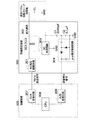
図3は、画像形成装置の現像高圧基板と制御基板の構成を示すブロック図である。尚、図3に示す構成は、本発明の印加手段、検出手段、制御手段を実現するための一例である。 FIG. 3 is a block diagram illustrating the configuration of the development high-voltage substrate and the control substrate of the image forming apparatus. The configuration shown in FIG. 3 is an example for realizing the applying means, detecting means, and controlling means of the present invention.
図3において、画像形成装置には、現像高圧基板300、制御基板305が装備されている。現像高圧基板300には、AC高圧駆動回路301(印加手段)、ACトランス302、DC高圧回路303(印加手段)、p−p電圧検出回路304(検出手段)、コンデンサC1、コンデンサC2、出力抵抗が実装されている。制御基板305には、A/D変換回路306、D/A変換回路307、CPU308(制御手段)が実装されている。
In FIG. 3, the image forming apparatus is equipped with a development high-
現像高圧基板300において、AC高圧駆動回路301は、現像ACバイアス電圧を生成し、現像スリーブ4aに供給する。DC高圧回路303は、現像DCバイアス電圧を生成し、現像スリーブ4aに供給する。p−p電圧検出回路304は、コンデンサC2の両端のピークツーピーク電圧(p−p電圧)をDC電圧に変換し、容量検出信号として取り出す。
In the development
制御基板305において、A/D変換回路306は、p−p電圧検出回路304から出力される容量検出信号をアナログ信号からデジタル信号に変換する。CPU308は、上記各部の制御を司るものであり、プログラムに基づき図6のフローチャートに示す処理を実行する。
In the
また、CPU308は、p−p電圧検出回路304の容量検出信号に基づき、換言すれば感光ドラム−現像スリーブ間容量(現像容量)に基づき、現像を含む画像形成を行う条件を変更する。画像形成を行う条件には、現像ACバイアス電圧のピークツーピーク値(p−p値)、現像DCバイアス電圧の電圧値、帯電DCバイアス電圧の電圧値(第5の実施の形態)、感光ドラム1を露光するレーザ光の光量(第6の実施の形態)を含む。D/A変換回路307は、CPU308から出力されるVp−p設定信号をデジタル信号からアナログ信号に変換する。
The
現像バイアス生成回路は、現像高圧基板300において、現像DCバイアス生成部(DC高圧回路303)と、現像ACバイアス生成部(AC高圧駆動回路301、ACトランス302)に大別される。ACトランス302の一次側には、AC高圧駆動回路301が並列に接続されている。これにより、ACトランス302の一次側は、AC高圧駆動回路301により駆動される。ACトランス302の二次側には、DC高圧回路303が直列に接続されると共に、容量検出のためにコンデンサC1、コンデンサC2が接続されている。
The development bias generation circuit is roughly divided into a development DC bias generation unit (DC high voltage circuit 303) and a development AC bias generation unit (AC high
ACトランス302の二次側は、感光ドラム1と現像スリーブ4aの間の容量である負荷容量CLと、コンデンサC1、C2の容量とに分割された容量分圧回路となっている。負荷容量CLが称呼値350pFの場合、CL、C1、C2の合成直列容量は297pFである。コンデンサのインピーダンスは容量の逆数であるから、現像ACバイアス電圧のうちコンデンサC2の両端に印加されるピークツーピーク電圧(p−p電圧):Vp−pは、計算上、2kV×297pF/0.1uF=5.94Vとなる。
The secondary side of the
本出願の発明者は、上記コンデンサC2の両端のp−p電圧:Vp−pについて次の測定を行った。即ち、Vp−pの測定値もほぼ上記計算値に近い6.02Vという結果が得られた。但し、感光ドラム1や現像スリーブ4aの各々の偏芯成分によりコンデンサC2の両端電圧も影響を受ける(動的S−Dギャップ変動)。そのため、Vp−pを測定する際は、感光ドラム1と現像スリーブ4aの回転を停止させ、S−Dギャップが所定値になるようにした状態で測定している。
The inventor of the present application performed the following measurement on the pp voltage Vp-p across the capacitor C2. That is, the measured value of Vp-p was 6.02 V, which was almost close to the calculated value. However, the voltage across the capacitor C2 is also affected by the eccentric components of the
また、本出願の発明者は、感光ドラム1と現像スリーブ4aの間に配置するスペーサとして、長さの異なるスペーサを用意して交換することで次の測定を行った。即ち、S−Dギャップを称呼値の300umから±20%変更し、S−Dギャップを240umと360umに各々設定した場合のコンデンサC2の両端の電圧を測定したところ、Vp−pで以下の結果が得られた。
In addition, the inventors of the present application prepared the following measurements by preparing and replacing spacers having different lengths as spacers arranged between the
S−Dギャップが240umの場合・・・C2両端電圧=7.2V
S−Dギャップが360umの場合・・・C2両端電圧=5.15V
上記S−DギャップとコンデンサC2の両端電圧の関係をグラフにしたものを図4に示す。図4において、黒点はコンデンサC2の両端電圧であり、黒点を結んだ実線はコンデンサC2の両端電圧を多項式で示したものである。S−Dギャップに反比例して感光ドラム−現像スリーブ間容量が変化し、その結果、S−Dギャップが広がるとコンデンサC2の両端電圧が小さくなることが分かる。つまり、コンデンサC2の両端のp−p電圧を測定することで、S−Dギャップの距離を検出することが可能である。
When the SD gap is 240 um, the voltage across C2 is 7.2V.
When the SD gap is 360 um ... the voltage across C2 = 5.15V
FIG. 4 is a graph showing the relationship between the SD gap and the voltage across the capacitor C2. In FIG. 4, the black dot is the voltage across the capacitor C2, and the solid line connecting the black dots represents the voltage across the capacitor C2 as a polynomial. It can be seen that the capacitance between the photosensitive drum and the developing sleeve changes in inverse proportion to the SD gap, and as a result, the voltage across the capacitor C2 decreases as the SD gap widens. That is, the distance of the SD gap can be detected by measuring the pp voltage across the capacitor C2.
そこで、本実施の形態では、図3に示したようにコンデンサC2の両端にp−p電圧検出回路304を接続する構成とすることで、p−p電圧検出回路304によりコンデンサC2の両端のp−p電圧をDC電圧に変換し、容量検出信号として取り出している。
Therefore, in the present embodiment, the pp
感光ドラム1が回転軸1aを介して回転すると共に現像スリーブ4aが回転軸4dを介して回転した状態では、感光ドラム1及び現像スリーブ4aの各々の偏芯成分により、S−Dギャップが変動(動的S−D変動)する。そのため、動的S−D変動分を平均化する必要がある。
In the state where the
動的S−D変動によりコンデンサC2の両端のp−p電圧が変動している例を図5に示す。図5において、細い実線はp−p電圧検出回路304によるp−p電圧の検出波形であり、黒点はコンデンサC2の両端のp−p電圧をサンプリングしたものであり、太い実線は平均値である。また、矢印で示す範囲は感光ドラム一周分である。動的S−D変動への影響度は感光ドラム1の偏芯によるものが大きい。現像スリーブ4aの偏芯によるものは振幅が小さく周期も短い。
FIG. 5 shows an example in which the pp voltage across the capacitor C2 varies due to dynamic SD variation. In FIG. 5, a thin solid line is a detection waveform of the pp voltage by the pp
そこで、本実施の形態では、動的S−D変動による影響を取り除くため、S−Dギャップの検出は次のように平均化する。即ち、感光ドラム1及び現像スリーブ4aを回転駆動した状態で、感光ドラム一周分の時間(感光ドラム1が1回転する時間)に感光ドラム1を例えば8等分した8箇所の点のサンプリングを行って平均化する。本実施の形態では、感光ドラム一周分の時間が500msであるため、62.5ms間隔のサンプリングとなり、図5の例で言えば、平均化したコンデンサC2の両端のp−p電圧は6.2Vである。
Therefore, in the present embodiment, detection of the SD gap is averaged as follows in order to remove the influence of the dynamic SD fluctuation. That is, in a state where the
現像高圧基板300のp−p電圧検出回路304は、コンデンサC2の両端のp−p電圧をDC電圧に変換して容量検出信号として取り出し、制御基板305のA/D変換回路306に入力する。A/D変換回路306は、容量検出信号をアナログ信号からデジタル信号に変換する。CPU308は、A/D変換回路306から入力された容量検出信号に基づき、感光ドラム−現像スリーブ間容量を検出すると共に、Vp−p設定値を決定する。
The pp
図6は、本実施の形態に係る画像形成装置の感光ドラム−現像スリーブ間容量の検出とコンデンサC2の両端のp−p電圧の設定値の決定に関わる処理を示すフローチャートである。 FIG. 6 is a flowchart showing processing related to the detection of the capacitance between the photosensitive drum and the developing sleeve and the determination of the set value of the pp voltage across the capacitor C2 of the image forming apparatus according to the present embodiment.
図6において、制御基板305のCPU308は、コンデンサC2の両端のp−p電圧:Vp−pを初期値である2kVに設定する(ステップS601)。次に、CPU308は、一次帯電器2に高圧を供給する帯電高圧回路(不図示)の出力と、現像スリーブ4aに高圧を供給するAC高圧駆動回路301の出力と、DC高圧回路303の出力をそれぞれON状態とする(ステップS602)。これにより、CPU308は、感光ドラム1と現像スリーブ4aを回転駆動した状態で、容量検出信号をA/D変換回路306を介して読み取る。
In FIG. 6, the
次に、CPU308は、感光ドラム一周分を例えば8等分した8箇所の点について容量検出信号のサンプリングを行い、サンプリングした容量検出信号の値を平均化する処理を行うことで動的S−D変動を平均化する(ステップS603)。次に、CPU308は、下記の表1に示すように容量検出信号の平均値に応じて、現像ACバイアス電圧のVp−p設定値を決定する(ステップS604)。
Next, the
即ち、表1において、容量検出信号(容量検出電圧)を3段階(〜5.34、5.35〜6.53、6.54〜)に分ける。容量検出電圧の称呼値5.94Vの±10%以内に相当する容量検出電圧の場合は、現像ACバイアス電圧を基準値の2.0kVp−pに設定するための信号をD/A変換回路307を介してVp−p設定信号として出力する。
That is, in Table 1, the capacitance detection signal (capacitance detection voltage) is divided into three stages (up to 5.34, 5.35 to 6.53, and 6.54 to). In the case of a capacitance detection voltage corresponding to within ± 10% of the nominal value of the capacitance detection voltage 5.94 V, a signal for setting the development AC bias voltage to a reference value of 2.0 kVp-p is a D /
また、称呼値5.94Vの+10%以上に相当する容量検出電圧の場合は、Vp−pを10%減じる。また、称呼値5.94Vの−10%以下に相当する容量検出電圧の場合は、Vp−pを10%増やす。 In the case of a capacitance detection voltage corresponding to + 10% or more of the nominal value of 5.94 V, Vp-p is reduced by 10%. In the case of a capacitance detection voltage corresponding to −10% or less of the nominal value of 5.94V, Vp−p is increased by 10%.

図5の例で言えば、平均化した容量検出電圧が6.2Vであったので、現像ACバイアス電圧の設定値は2.0kVp−pとなる。 In the example of FIG. 5, since the averaged capacitance detection voltage is 6.2 V, the set value of the development AC bias voltage is 2.0 kVp-p.
感光ドラム−現像スリーブ間容量(現像容量)のサンプリングは、画像形成装置の立上げ時(例えば当日の朝の最初の立上げ時)に行うようにしてもよい。また、前記サンプリングは、S−Dギャップが画像形成装置の機内温度によって変動する場合には、画像形成を行った用紙の枚数が所定枚数に達する毎にもしくは画像形成装置の稼動時間が所定時間に達する毎に行うようにしてもよい。 Sampling of the capacity between the photosensitive drum and the developing sleeve (developing capacity) may be performed when the image forming apparatus is started up (for example, at the first start-up in the morning of the day). In the sampling, when the SD gap varies depending on the temperature inside the image forming apparatus, every time the number of sheets on which the image is formed reaches a predetermined number or the operation time of the image forming apparatus is set to a predetermined time. It may be performed every time it reaches.
尚、本実施の形態では、現像ACバイアス電圧を切り替えるための容量検出信号のランクを3つに分けて制御したが、これに限定されるものではない。感光ドラム−現像スリーブ間容量の測定値に応じて現像ACバイアス電圧を無段階に設定するようにしてもよい。 In this embodiment, the rank of the capacitance detection signal for switching the development AC bias voltage is divided into three levels, but the present invention is not limited to this. The developing AC bias voltage may be set steplessly according to the measured value of the capacitance between the photosensitive drum and the developing sleeve.
以上説明したように本実施の形態によれば、上記制御を行うことにより、実際のS−Dギャップに対応した現像ACバイアス電圧のVp−p設定値を決定することが可能となる。これに伴い、現像バイアス電圧を適正に設定することが可能となると共にそれに合わせた帯電バイアス電圧の設定が可能となる。これにより、現像性を向上させた上で、画像不良の発生を抑制することが可能となると共に画像濃度を一定に保つことが可能となる。 As described above, according to the present embodiment, it is possible to determine the Vp-p set value of the development AC bias voltage corresponding to the actual SD gap by performing the above control. As a result, the development bias voltage can be set appropriately and the charging bias voltage can be set accordingly. As a result, it is possible to improve the developability, suppress the occurrence of image defects, and keep the image density constant.
〔第2の実施の形態〕
本発明の第2の実施の形態は、上記第1の実施の形態に対して、現像ACバイアス電圧の設定を制御基板のCPUからの指令ではなく現像高圧基板内でフィードバック制御により行う点において相違する。本実施の形態のその他の要素は、上記第1の実施の形態(図1、図2)の対応するものと同一なので説明を省略する。
[Second Embodiment]
The second embodiment of the present invention is different from the first embodiment in that the setting of the development AC bias voltage is performed by feedback control in the development high voltage substrate instead of a command from the CPU of the control substrate. To do. Since the other elements of the present embodiment are the same as the corresponding ones of the first embodiment (FIGS. 1 and 2), description thereof is omitted.
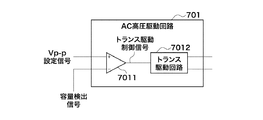
図7は、本実施の形態に係る画像形成装置の現像高圧基板と制御基板の構成を示すブロック図である。図8は、図7のAC高圧駆動回路の詳細構成を示すブロック図である。尚、図7に示す構成は、本発明の印加手段、検出手段、制御手段を実現するための一例である。 FIG. 7 is a block diagram showing the configuration of the development high-voltage board and the control board of the image forming apparatus according to the present embodiment. FIG. 8 is a block diagram showing a detailed configuration of the AC high voltage drive circuit of FIG. The configuration shown in FIG. 7 is an example for realizing the application means, detection means, and control means of the present invention.
図7、図8において、画像形成装置には、現像高圧基板700、制御基板705が装備されている。現像高圧基板700には、AC高圧駆動回路701(印加手段)、ACトランス702、DC高圧回路703(印加手段)、p−p電圧検出回路704(検出手段、制御手段)、コンデンサC1、コンデンサC2、出力抵抗が実装されている。更に、AC高圧駆動回路701は、誤差増幅器7011、トランス駆動回路7012から構成されている。制御基板705には、D/A変換回路707、CPU708(制御手段)が実装されている。
7 and 8, the image forming apparatus is equipped with a development high-
図7の構成では、図3の構成とは異なり、現像高圧基板700において感光ドラム−現像スリーブ間容量の検出値がAC高圧駆動回路701に入力される。即ち、AC高圧駆動回路701の誤差増幅器7011には、p−p電圧検出回路704から容量検出信号が入力される。また、誤差増幅器7011には、制御基板705のD/A変換回路707からVp−p設定信号が入力される。誤差増幅器7011は、Vp−p設定信号と容量検出信号に基づき、トランス駆動制御信号をトランス駆動回路7012に出力する。
In the configuration of FIG. 7, unlike the configuration of FIG. 3, the detected value of the capacitance between the photosensitive drum and the developing sleeve in the developing high-
トランス駆動回路7012は、トランス駆動制御信号が設定値より小さい場合はACトランス702の一次側駆動電圧を小さくし、トランス駆動制御信号が設定値より大きい場合はACトランス702の一次側駆動電圧を大きくする。その結果、次のフィードバック制御が行われる。
The
Vp−p設定信号に比較して容量検出信号が小さい場合は、トランス駆動回路7012は、Vp−pを大きくするトランス駆動制御電圧をACトランス702に出力する。他方、Vp−p設定信号に比較して容量検出信号が大きい場合は、トランス駆動回路7012は、Vp−pを小さくするトランス駆動制御電圧をACトランス702に出力する。
When the capacitance detection signal is smaller than the Vp-p setting signal, the
図4から分かるように、S−Dギャップが小さい場合は感光ドラム−現像スリーブ間容量の検出値が大きくなるため、検出値が所定値になるようにトランス駆動制御電圧を出力する。これにより、S−Dギャップが小さい場合はAC高圧駆動回路301のVp−p出力が小さくなり、S−Dギャップが大きい場合はAC高圧駆動回路301のVp−p出力が大きくなる。
As can be seen from FIG. 4, when the SD gap is small, the detected value of the capacitance between the photosensitive drum and the developing sleeve is large, so that the transformer drive control voltage is output so that the detected value becomes a predetermined value. As a result, when the SD gap is small, the Vp-p output of the AC high
本実施の形態では、Vp−pを制御することでリングマークの発生を抑制し、現像性を安定化させることが可能となる。尚、S−Dギャップの変動で画像濃度が変動する場合は、感光ドラム−現像スリーブ間容量の検出値に応じて現像DCバイアス電圧の値を制御することで、画像濃度を一定に保ち画像濃度の帯ムラ等の画像不良を抑制することが可能となる。 In the present embodiment, by controlling Vp-p, it is possible to suppress the generation of ring marks and to stabilize developability. When the image density changes due to the change in the SD gap, the image density is kept constant by controlling the value of the development DC bias voltage according to the detected value of the capacitance between the photosensitive drum and the developing sleeve. It is possible to suppress image defects such as band unevenness.
以上説明したように本実施の形態によれば、現像性を向上させた上で、画像不良の発生を抑制することが可能となると共に画像濃度を一定に保つことが可能となる。 As described above, according to the present embodiment, it is possible to suppress the occurrence of image defects and maintain a constant image density while improving developability.
〔第3の実施の形態〕
本発明の第3の実施の形態は、上記第1の実施の形態に対して、現像ACバイアス電圧のVp−p設定値の変更をユーザ或いはサービス員が操作部を操作することで行う点において相違する。本実施の形態のその他の要素は、上記第1の実施の形態(図1、図2)の対応するものと同一なので説明を省略する。
[Third Embodiment]
The third embodiment of the present invention is different from the first embodiment in that the Vp-p set value of the development AC bias voltage is changed by the user or service staff operating the operation unit. Is different. Since the other elements of the present embodiment are the same as the corresponding ones of the first embodiment (FIGS. 1 and 2), description thereof is omitted.
図9は、本実施の形態に係る画像形成装置の現像高圧基板と制御基板の構成を示すブロック図である。尚、図9に示す構成は、本発明の印加手段、検出手段、制御手段、表示手段、設定手段を実現するための一例である。 FIG. 9 is a block diagram illustrating the configuration of the development high-voltage board and the control board of the image forming apparatus according to the present embodiment. The configuration shown in FIG. 9 is an example for realizing the application means, detection means, control means, display means, and setting means of the present invention.
図9において、画像形成装置には、現像高圧基板900、制御基板905が装備されている。現像高圧基板900には、AC高圧駆動回路901(印加手段)、ACトランス902、DC高圧回路903(印加手段)、p−p電圧検出回路904(検出手段)、コンデンサC1、コンデンサC2、出力抵抗が実装されている。制御基板905には、A/D変換回路906、D/A変換回路907、CPU908(制御手段)が実装されている。更に、制御基板905のCPU908には、操作部909(表示手段、設定手段)が信号線により接続されている。
In FIG. 9, the image forming apparatus is equipped with a development high-
操作部909は、図10に示すように表示パネル1001、キーボード1002を備えている。p−p電圧検出回路904により検出されCPU908によりサンプリングされた感光ドラム−現像スリーブ間容量の検出値(容量を示す情報)は、操作部909の表示パネル1001に電圧値で表示される。
The
サービス員(操作者)はS−Dギャップの変動につながると判断した感光ドラム1または現像器4のメンテナンス或いは交換を行った後で、表示パネル1001に表示された感光ドラム−現像スリーブ間容量の検出値(電圧値)を確認する。更に、サービス員は表示パネル1001の表示内容の確認に基づき、Vp−p設定値が適正な値になるようにキーボード1002のキー操作により設定値を変更する。この処理を図11で詳細に説明する。
The service staff (operator) performs maintenance or replacement of the
図11は、画像形成装置の感光ドラム−現像スリーブ間容量の検出とコンデンサC2の両端のp−p電圧の設定値の変更に関わる処理を示すフローチャートである。 FIG. 11 is a flowchart showing processing relating to detection of the capacitance between the photosensitive drum and the developing sleeve of the image forming apparatus and change of the set value of the pp voltage across the capacitor C2.
図11において、制御基板905のCPU908は、感光ドラム−現像スリーブ間容量を検出する現像容量検出モードによる処理を開始する(ステップS1101)。まず、CPU908は、コンデンサC2の両端のp−p電圧:Vp−pを初期値である2kVに設定する(ステップS1111)。次に、CPU908は、一次帯電器2に高圧を供給する帯電高圧回路(不図示)の出力と、現像スリーブ4aに高圧を供給するAC高圧駆動回路901の出力をそれぞれON状態とする(ステップS1112)。これにより、CPU908は、感光ドラム1と現像スリーブ4aを回転駆動した状態で、容量検出信号をA/D変換回路906を介して読み取る。
In FIG. 11, the
次に、CPU908は、感光ドラム一周分を例えば8等分した8箇所の点について容量検出信号のサンプリングを行い、サンプリングした容量検出信号の値を平均化する処理を行う(ステップS1113)。次に、CPU908は、操作部909の表示パネル1001に容量検出信号に相当する容量検出電圧値を表示する(ステップS1114)。サービス員は表示に基づき操作部909を介して、容量検出電圧値が大きい場合はVp−p設定値を小さくし、容量検出電圧値が小さい場合はVp−p設定値を大きくする。CPU908は、入力されたVp−p設定値に応じた制御を行う(ステップS1102)。
Next, the
以上説明したように本実施の形態によれば、現像性を向上させた上で、画像不良の発生を抑制することが可能となると共に画像濃度を一定に保つことが可能となる。 As described above, according to the present embodiment, it is possible to suppress the occurrence of image defects and maintain a constant image density while improving developability.
〔第4の実施の形態〕
本発明の第4の実施の形態は、上記第1の実施の形態に対して、現像器4で1成分現像剤(磁性体を含むトナーからなる現像剤)を用いる点において相違する。更に、現像ACバイアスを用いて感光ドラム−現像スリーブ間容量を検出する点は上記第1の実施の形態と同様であるが、検出結果により現像DCバイアス電圧の条件(画像形成を行う条件)を変更する点において相違する。本実施の形態のその他の要素は、上記第1の実施の形態(図1〜図3)の対応するものと同一なので説明を省略する。
[Fourth Embodiment]
The fourth embodiment of the present invention is different from the first embodiment in that the developing
本実施の形態では1成分現像剤を用いる。即ち、1成分現像剤を用いて感光ドラム1の静電潜像を現像する際は、現像スリーブ4aの現像剤の穂が感光ドラム1と接触せず、現像スリーブ4aと感光ドラム1の間の電界により現像剤が飛翔する現象(ジャンピング現像)を利用して現像を行う。
In this embodiment, a one-component developer is used. That is, when the electrostatic latent image on the
図12は、本実施の形態に係る画像形成装置の感光ドラム−現像スリーブ間容量の検出と現像DCバイアス電圧設定値の決定に関わる処理を示すフローチャートである。 FIG. 12 is a flowchart showing processing relating to detection of the capacitance between the photosensitive drum and the developing sleeve and determination of the development DC bias voltage setting value of the image forming apparatus according to the present embodiment.
図12において、制御基板305のCPU308は、コンデンサC2の両端のp−p電圧:Vp−pを初期値である2kVに設定する(ステップS1201)。次に、CPU308は、一次帯電器2に高圧を供給する帯電高圧回路(不図示)の出力と、現像スリーブ4aに高圧を供給するAC高圧駆動回路301の出力と、DC高圧回路303の出力をそれぞれON状態とする(ステップS1202)。これにより、CPU308は、感光ドラム1と現像スリーブ4aを回転駆動した状態で、容量検出信号をA/D変換回路306を介して読み取る。
In FIG. 12, the
次に、CPU308は、感光ドラム一周分を例えば8等分した8箇所の点について容量検出信号のサンプリングを行い、サンプリングした容量検出信号の値を平均化する処理を行うことで動的S−D変動を平均化する(ステップS1203)。次に、CPU308は、下記の表2に示すように容量検出信号の平均値に応じて現像DCバイアス電圧の設定値を決定する(ステップS1204)。
Next, the
即ち、表2において、容量検出信号(容量検出電圧)を3段階(〜5.34、5.35〜6.53、6.54〜)に分ける。容量検出電圧の称呼値5.94Vの±10%以内に相当する容量検出電圧の場合は、現像DCバイアス電圧を基準値の−400Vに設定するための信号をD/A変換回路307を介してDC高圧設定信号として出力する。現像DCバイアス電圧の設定値が−400Vの時の帯電バイアス電圧の設定値は−600Vである。
That is, in Table 2, the capacitance detection signal (capacitance detection voltage) is divided into three stages (up to 5.34, 5.35 to 6.53, and 6.54 to). In the case of a capacitance detection voltage corresponding to a nominal value of the capacitance detection voltage of 5.94 V within ± 10%, a signal for setting the development DC bias voltage to the reference value of −400 V is passed through the D /
また、称呼値5.94Vの+10%以上に相当する容量検出電圧の場合は、コントラスト電位Vcontを25V小さくするために現像DCバイアス電圧を−375Vに設定する。現像DCバイアス電圧の設定値が−375Vの時の帯電バイアス電圧の設定値は−575Vである。また、称呼値5.94Vの−10%以下に相当する容量検出電圧の場合は、コントラスト電位Vcontを25V大きくするために現像DCバイアス電圧を−425Vに設定する。現像DCバイアス電圧の設定値が−425Vの時の帯電バイアス電圧の設定値は−625Vである。 In the case of a capacitance detection voltage corresponding to + 10% or more of the nominal value 5.94V, the development DC bias voltage is set to -375V in order to reduce the contrast potential Vcont by 25V. When the setting value of the development DC bias voltage is −375V, the setting value of the charging bias voltage is −575V. In the case of the capacitance detection voltage corresponding to −10% or less of the nominal value 5.94V, the development DC bias voltage is set to −425V in order to increase the contrast potential Vcont by 25V. When the setting value of the development DC bias voltage is −425V, the setting value of the charging bias voltage is −625V.
現像DCバイアス電圧の設定値は、称呼値のS−Dギャップ=300umの時に、画像に所定の濃度を出すためのコントラスト電位VcontがVcont=250Vとなるように、上記の−400Vを基準値としている。 The set value of the development DC bias voltage is set to the above--400 V as a reference value so that the contrast potential Vcont for giving a predetermined density to the image becomes Vcont = 250 V when the nominal SD gap is 300 μm. Yes.
容量検出信号が大きく検出された(容量検出電圧が大きい)場合は、S−Dギャップが小さくなっているため、その分、コントラスト電位Vcontが小さくなるように制御する。逆に、容量検出信号が小さく検出された(容量検出電圧が小さい)場合は、S−Dギャップが大きくなっているため、その分、コントラスト電位Vcontが大きくなるように制御する。これにより、S−Dギャップの違い(大小)による画像濃度への影響を減らしている。 When the capacitance detection signal is detected large (capacity detection voltage is large), since the SD gap is small, control is performed so that the contrast potential Vcont is reduced accordingly. Conversely, when the capacitance detection signal is detected to be small (capacitance detection voltage is small), the SD gap is large, so that the control is performed so that the contrast potential Vcont increases accordingly. Thereby, the influence on the image density due to the difference (large or small) in the SD gap is reduced.
また、コントラスト電位Vcontの変更により、かぶり取り電位Vbackが変化するため、かぶり取り電位Vbackが一定になるように更に帯電電位を変更することも効果がある。 Further, since the fog removal potential Vback is changed by changing the contrast potential Vcont, it is also effective to further change the charging potential so that the fog removal potential Vback becomes constant.
図5の例で言えば、平均化した容量検出電圧が6.2Vであったので、現像DCバイアス電圧の設定値は−400Vとなる。 In the example of FIG. 5, since the averaged capacitance detection voltage is 6.2V, the setting value of the development DC bias voltage is −400V.
感光ドラム−現像スリーブ間容量(現像容量)のサンプリングは、画像形成装置の立上げ時(例えば当日の朝の最初の立上げ時)に行うようにしてもよい。また、前記サンプリングは、S−Dギャップが画像形成装置の機内温度によって変動する場合には、画像形成を行った用紙の枚数が所定枚数に達する毎にもしくは画像形成装置の稼動時間が所定時間に達する毎に行うようにしてもよい。 Sampling of the capacity between the photosensitive drum and the developing sleeve (developing capacity) may be performed when the image forming apparatus is started up (for example, at the first start-up in the morning of the day). In the sampling, when the SD gap varies depending on the temperature inside the image forming apparatus, every time the number of sheets on which the image is formed reaches a predetermined number or the operation time of the image forming apparatus is set to a predetermined time. It may be performed every time it reaches.
尚、本実施の形態では、現像DCバイアス電圧を切り替えるための容量検出信号のランクを3つに分けて制御したが、これに限定されるものではない。感光ドラム−現像スリーブ間容量の測定値に応じて現像DCバイアス電圧を無段階に設定するようにしてもよい。 In this embodiment, the rank of the capacitance detection signal for switching the development DC bias voltage is controlled by dividing the rank into three. However, the present invention is not limited to this. The development DC bias voltage may be set steplessly according to the measured value of the capacitance between the photosensitive drum and the development sleeve.
以上説明したように本実施の形態によれば、現像性を向上させた上で、画像不良の発生を抑制することが可能となると共に画像濃度を一定に保つことが可能となる。 As described above, according to the present embodiment, it is possible to suppress the occurrence of image defects and maintain a constant image density while improving developability.
[第5の実施の形態]
本発明の第5の実施の形態は、上記第1の実施の形態に対して、現像DCバイアス電圧の設定値の変更をユーザ或いはサービス員が操作部を操作することで行う点において相違する。本実施の形態のその他の要素は、上記第1の実施の形態(図1、図2)、上記第3の実施の形態(図9)の対応するものと同一なので説明を省略する。
[Fifth Embodiment]
The fifth embodiment of the present invention is different from the first embodiment in that the setting value of the development DC bias voltage is changed by the user or a service person operating the operation unit. The other elements of the present embodiment are the same as the corresponding ones of the first embodiment (FIGS. 1 and 2) and the third embodiment (FIG. 9), and thus description thereof is omitted.
図13は、本実施の形態に係る画像形成装置の感光ドラム−現像スリーブ間容量の検出と現像DCバイアス電圧の設定値の変更に関わる処理を示すフローチャートである。 FIG. 13 is a flowchart showing processing relating to the detection of the capacitance between the photosensitive drum and the developing sleeve and the change of the setting value of the developing DC bias voltage in the image forming apparatus according to the present embodiment.
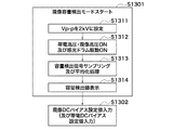
図13において、制御基板905のCPU908は、感光ドラム−現像スリーブ間容量を検出する現像容量検出モードによる処理を開始する(ステップS1301)。まず、CPU908は、コンデンサC2の両端のp−p電圧:Vp−pを初期値である2kVに設定する(ステップS1311)。次に、CPU908は、一次帯電器2に高圧を供給する帯電高圧回路(不図示)の出力と、現像スリーブ4aに高圧を供給するAC高圧駆動回路901の出力と、DC高圧回路903の出力をそれぞれON状態とする(ステップS1312)。これにより、CPU908は、感光ドラム1と現像スリーブ4aを回転駆動した状態で、容量検出信号をA/D変換回路906を介して読み取る。
In FIG. 13, the
次に、CPU908は、感光ドラム一周分を例えば8等分した8箇所の点について容量検出信号のサンプリングを行い、サンプリングした容量検出信号の値を平均化する処理を行う(ステップS1313)。次に、CPU908は、操作部909の表示パネル1001に容量検出信号に相当する容量検出電圧値を表示する(ステップS1314)。サービス員は表示に基づき操作部909を介して、容量検出電圧値が大きい場合は現像DCバイアス電圧の設定値を小さくし、容量検出電圧値が小さい場合は現像DCバイアス電圧の設定値を大きくする。CPU908は、入力された現像DCバイアス電圧の設定値に応じた制御を行う(ステップS1302)。
Next, the
現像DCバイアス電圧の設定は現像DCバイアス電圧の電圧を入力するようにしてもよいし、コントラスト電位Vcontの値を調整するようにしてもよい。また、上記第4の実施の形態で説明したように現像DCバイアス電圧の設定を変更することでかぶり取り電位Vbackも影響を受けるため、現像DCバイアス電圧の設定に応じて帯電バイアス電圧の設定値も変更されるようにした方が好適である。 The development DC bias voltage may be set by inputting the development DC bias voltage or adjusting the contrast potential Vcont. Further, since the fog removal potential Vback is also affected by changing the setting of the development DC bias voltage as described in the fourth embodiment, the setting value of the charging bias voltage according to the setting of the development DC bias voltage. It is preferable to change the above.
以上説明したように本実施の形態によれば、現像性を向上させた上で、画像不良の発生を抑制することが可能となると共に画像濃度を一定に保つことが可能となる。 As described above, according to the present embodiment, it is possible to suppress the occurrence of image defects and maintain a constant image density while improving developability.
[第6の実施の形態]
本発明の第6の実施の形態は、上記第1の実施の形態に対して、現像器4で2成分現像剤ではなく1成分現像剤を用いる点において相違する。更に、現像ACバイアス電圧を用いて感光ドラム−現像スリーブ間容量を検出する点は上記第1の実施の形態と同様であるが、検出結果により現像バイアス電圧の条件(画像形成を行う条件)を変更する点において相違する。
[Sixth Embodiment]
The sixth embodiment of the present invention is different from the first embodiment in that the developing
図14は、本実施の形態に係る画像形成装置の感光ドラムの回転軸と現像スリーブの回転軸がスペーサにより位置決めされている状態を示す構成図である。 FIG. 14 is a configuration diagram showing a state in which the rotating shaft of the photosensitive drum and the rotating shaft of the developing sleeve of the image forming apparatus according to the present embodiment are positioned by the spacer.
図14において、感光ドラム1の端部には、ホームポジション(以下HP)フラグ1401が設けられている。また、感光ドラム1の近傍には、HPセンサ1402が配置されている。HPセンサ1402は、HPフラグ1401を読み取り、感光ドラム1のHPを検出したことを示すHP信号をCPU(図15)に出力する。HPフラグ1401をHPセンサ1402で読み取る構成以外は、図2の構成と同様であり同様箇所の説明は省略する。
In FIG. 14, a home position (hereinafter HP)
本実施の形態では、スペーサ201によって位置決めされた感光ドラム1と現像スリーブ4aとの間の距離(S−Dギャップ)は、称呼値で300umに設定されている。この場合、S−Dギャップは感光ドラム1の偏芯により±30umずれる可能性があり、S−Dギャップの平均距離が300umの場合でも感光ドラム1の回転により、S−Dギャップの最小値は270um、S−Dギャップの最大値は330umとなる。
In the present embodiment, the distance (SD gap) between the
感光ドラム1の表面は一次帯電器2により例えば−600Vに帯電される。感光ドラム1の表面にレーザ光により形成される静電潜像(潜像部)の電位は−150Vとなっている。現像DCバイアスとして−400Vが現像スリーブ4aに印加されることで、画像濃度を決定するためのコントラスト電位Vcontが250V、かぶりを防ぐためのかぶり取り電位Vbackが200Vになる。
The surface of the
本実施の形態では、現像バイアス電圧として、図18に示した矩形波のバイアス電圧を使用している。DC成分(DCバイアス)にAC成分(ACバイアス)を加えることで、画像のがさつきを抑制することが可能となると共に画像濃度を十分に得ることが可能となる。S−Dギャップが称呼値の場合、現像ACバイアス電圧のパルス部のVp−pは2kVである。また、S−Dギャップが称呼値の場合、感光ドラム1と現像スリーブ4aの間の容量性負荷は350pFである。
In this embodiment, the rectangular bias voltage shown in FIG. 18 is used as the developing bias voltage. By adding an AC component (AC bias) to a DC component (DC bias), it becomes possible to suppress the roughness of the image and to obtain a sufficient image density. When the SD gap is a nominal value, Vp-p of the pulse part of the development AC bias voltage is 2 kV. When the SD gap is a nominal value, the capacitive load between the
図15は、画像形成装置の現像高圧基板と制御基板の構成を示すブロック図である。尚、図15に示す構成は、本発明の印加手段、検出手段、制御手段、記憶手段を実現するための一例である。 FIG. 15 is a block diagram illustrating the configuration of the development high-voltage board and the control board of the image forming apparatus. The configuration shown in FIG. 15 is an example for realizing the applying means, detecting means, control means, and storage means of the present invention.
図15において、画像形成装置には、現像高圧基板1500、制御基板1505、帯電高圧基板1513が装備されている。現像高圧基板1500には、AC高圧駆動回路1501(印加手段)、ACトランス1502、DC高圧回路1503(印加手段)、p−p電圧検出回路1504(検出手段)、コンデンサC1、コンデンサC2、出力抵抗が実装されている。制御基板1505には、A/D変換回路1506、D/A変換回路1507、CPU1508(制御手段)、D/A変換回路1509、D/A変換回路1510、メモリ1511(記憶手段)が実装されている。帯電高圧基板1513には、DC高圧回路1514が実装されている。
In FIG. 15, the image forming apparatus is equipped with a development high-
図15における図3との相違点を中心に説明する。p−p電圧検出回路1504によりコンデンサC2の両端の電圧をDC電圧(容量検出信号)に変換し、A/D変換回路1506により容量検出信号をアナログ信号からデジタル信号に変換し、CPU1508により読み取る。メモリ1511は、CPU1508に接続されており、CPU1508で読み取ったデジタルの容量検出信号の変動を記憶する。D/A変換回路1509は、DC高圧回路1503の出力電圧を制御する。D/A変換回路1510は、DC高圧回路1514の出力電圧を制御する。
The description will focus on the differences in FIG. 15 from FIG. The voltage at both ends of the capacitor C2 is converted into a DC voltage (capacitance detection signal) by the pp
本出願の発明者は、感光ドラム1と現像スリーブ4aの間に配置するスペーサとして、長さの異なるスペーサを用意して交換することで次の測定を行った。即ち、S−Dギャップを称呼値の300umから動的に変動する可能性のある増減分として±10%変更し、S−Dギャップを270umと330umに各々設定した場合のコンデンサC2の両端電圧を測定したところ、Vp−pで以下の結果が得られた。
The inventor of the present application made the following measurement by preparing and replacing a spacer having a different length as a spacer disposed between the
S−Dギャップが270umの場合・・・C2両端電圧=6.60V
S−Dギャップが330umの場合・・・C2両端電圧=5.61V
図4で示したようにS−Dギャップに反比例して感光ドラム−現像スリーブ間容量が変化し、その結果、S−Dギャップが広がるとコンデンサC2の両端電圧が小さくなることが分かる。つまり、コンデンサC2の両端のp−p電圧を測定することで、S−Dギャップの距離を検出することが可能である。
When the SD gap is 270 um, the voltage across C2 is 6.60V.
When SD gap is 330 um: Voltage across C2 = 5.61V
As shown in FIG. 4, it can be seen that the capacitance between the photosensitive drum and the developing sleeve changes in inverse proportion to the SD gap, and as a result, the voltage across the capacitor C2 decreases as the SD gap widens. That is, the distance of the SD gap can be detected by measuring the pp voltage across the capacitor C2.
そこで、本実施の形態では、コンデンサC2の両端にp−p電圧検出回路1504を接続する構成とすることで、p−p電圧検出回路1504によりコンデンサC2の両端のp−p電圧をDC電圧に変換し、容量検出信号として取り出している。
Therefore, in the present embodiment, the pp
感光ドラム1が回転軸1aを介して回転すると共に現像スリーブ4aが回転軸4dを介して回転した状態では、感光ドラム1及び現像スリーブ4aの各々の偏芯成分により、S−Dギャップが変動(動的S−D変動)する。
In the state where the
動的S−D変動によりコンデンサC2の両端のp−p電圧が変動している例を図16に示す。図16において、細い実線はp−p電圧検出回路1504によるp−p電圧の検出波形であり、黒点はコンデンサC2の両端のp−p電圧をサンプリングしたものであり、太い実線は平均値であり、パルス波形はHP信号である。動的S−D変動への影響度は感光ドラム1の偏芯によるものが大きい。現像スリーブ4aの偏芯によるものは振幅が小さく周期も短い。
FIG. 16 shows an example in which the pp voltage across the capacitor C2 varies due to dynamic SD variation. In FIG. 16, a thin solid line is a detection waveform of the pp voltage by the pp
そこで、本実施の形態では、動的S−D変動の影響を取り除くため、S−Dギャップの検出は次のように平均化する。即ち、感光ドラム1及び現像スリーブ4aを回転駆動した状態で、HPセンサ1402から出力されるHP信号を基準として、感光ドラム一周あたり例えば8等分した8箇所の点のサンプリングを行って平均化する。本実施の形態では、感光ドラム一周分の時間が500msであるため、62.5ms間隔のサンプリングとなる。
Therefore, in this embodiment, in order to remove the influence of the dynamic SD fluctuation, the detection of the SD gap is averaged as follows. In other words, with the
現像高圧基板1500のp−p電圧検出回路1504は、コンデンサC2の両端のp−p電圧をDC電圧に変換して容量検出信号として取り出し、制御基板1505のA/D変換回路1506に入力する。CPU1508は、A/D変換回路1506から入力された容量検出信号に基づき、感光ドラム−現像スリーブ間容量を検出すると共に、S−Dギャッププロファイルを取得する。
The pp
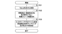
図17は、画像形成装置のS−Dギャッププロファイルの取得に関わる処理を示すフローチャートである。 FIG. 17 is a flowchart illustrating processing relating to acquisition of the SD gap profile of the image forming apparatus.
図17において、制御基板1505のCPU1508は、コンデンサC2の両端のp−p電圧:Vp−pを初期値である2kVに設定する(ステップS1711)。次に、CPU1508は、一次帯電器2に高圧を供給するDC高圧回路1514の出力と、現像スリーブ4aに高圧を供給するAC高圧駆動回路1501の出力と、DC高圧回路1503の出力をそれぞれON状態とする(ステップS1702)。これにより、CPU1508は、感光ドラム1と現像スリーブ4aを回転駆動した状態で、容量検出信号をA/D変換回路1506を介して読み取る。
In FIG. 17, the
次に、CPU1508は、感光ドラム一周あたり例えば8等分した8箇所の点について且つ感光ドラム四周分について容量検出信号のサンプリングを行い、サンプリングした容量検出信号の値を平均化する処理を行い、処理結果をメモリ1511に記憶する。このように感光ドラム一周あたり8箇所の点を感光ドラム四周分について平均する。これにより、CPU1508は、感光ドラム1の偏芯以外(例えば現像スリーブ4aの偏芯)が原因となって発生する微小な振れを除去することで、動的S−D変動のプロファイル(S−Dギャッププロファイル)を取得する(ステップS1703)。
Next, the
p−p電圧検出回路1504の出力である容量検出信号(容量検出電圧)とS−Dギャップの関係から、上記の各測定点のS−Dギャップを算出し、S−Dギャップの変動による濃度変動を打ち消すように現像DCバイアス電圧を決定し制御する。これにより、動的S−D変動による濃度ムラの無い画像を得ることができる。
The SD gap at each measurement point is calculated from the relationship between the capacitance detection signal (capacitance detection voltage), which is the output of the pp
上述したように、本実施の形態では、S−Dギャップが中央値の300umの場合、コントラスト電位Vcontを250Vに設定している。S−Dギャップが10%狭くなって270umになった時の濃度をS−Dギャップの中央値と同じようにする場合は、Vcontを30V小さくする必要がある。S−Dギャップが10%広くなった場合は、Vcontを30V大きくして濃度を補ってやる必要がある。また、現像バイアスを変化させた場合は、かぶり取り電位Vbackが変動するため、帯電DCバイアス電圧を同時に制御して、Vbackを一定にすることが好ましい。 As described above, in the present embodiment, the contrast potential Vcont is set to 250 V when the SD gap has a median value of 300 μm. In order to make the concentration when the SD gap becomes 10% narrower and 270 μm the same as the median value of the SD gap, Vcont needs to be reduced by 30V. When the SD gap becomes 10% wider, it is necessary to compensate for the concentration by increasing Vcont by 30V. Further, when the developing bias is changed, the fog removal potential Vback fluctuates. Therefore, it is preferable to control the charging DC bias voltage at the same time to make Vback constant.
図17に示した処理で取得したS−Dギャッププロファイルを用いて、現像DCバイアス電圧と帯電DCバイアス電圧を求めたものを下記の表3に示す。 Table 3 below shows the development DC bias voltage and the charging DC bias voltage obtained using the SD gap profile obtained by the processing shown in FIG.
感光ドラム−現像スリーブ間容量(現像容量)のサンプリングは、画像形成装置の立上げ時(例えば当日の朝の最初の立上げ時)に行うようにしてもよい。また、前記サンプリングは、S−Dギャップが画像形成装置の機内温度によって変動する場合には、画像形成を行った用紙の枚数が所定枚数に達する毎にもしくは画像形成装置の稼動時間が所定時間に達する毎に行うようにしてもよい。 Sampling of the capacity between the photosensitive drum and the developing sleeve (developing capacity) may be performed when the image forming apparatus is started up (for example, at the first start-up in the morning of the day). In the sampling, when the SD gap varies depending on the temperature inside the image forming apparatus, every time the number of sheets on which the image is formed reaches a predetermined number or the operation time of the image forming apparatus is set to a predetermined time. It may be performed every time it reaches.
尚、本実施の形態では、濃度安定化のためにVcontを制御するにあたり、S−Dギャップ変動に合わせて現像DCバイアス電圧を変更するようにしたが、これに限定されるものではない。感光ドラム1の潜像部の電位を変化させるために感光ドラム1を露光するレーザ光の光量を変更してもよい。
In this embodiment, when controlling Vcont for density stabilization, the development DC bias voltage is changed in accordance with the SD gap fluctuation, but the present invention is not limited to this. In order to change the potential of the latent image portion of the
また、本実施の形態では、上記第1の実施の形態と同様、動的S−D変動により感光ドラム−現像スリーブ間の現像ACバイアス電圧による電界が過大/過少になることで、リングマークの発生や現像性の低下が起きる可能性がある。そこで、取得したS−Dギャッププロファイルに応じて、現像ACバイアス電圧のVp−pを制御することも有効である。 Further, in the present embodiment, as in the first embodiment, the electric field due to the development AC bias voltage between the photosensitive drum and the developing sleeve is excessively / decreased due to the dynamic SD fluctuation, and thus the ring mark is changed. Occurrence and deterioration of developability may occur. Therefore, it is also effective to control the development AC bias voltage Vp-p according to the acquired SD gap profile.
以上説明したように本実施の形態によれば、実際のS−Dギャップに合った現像DCバイアスを設定することが可能となる。これにより、現像性を向上させた上で、画像不良の発生を抑制することが可能となると共に画像濃度を一定に保つことが可能となる。更に、無駄なトナー消費を抑制することも可能となる。 As described above, according to the present embodiment, it is possible to set the development DC bias that matches the actual SD gap. As a result, it is possible to improve the developability, suppress the occurrence of image defects, and keep the image density constant. Furthermore, wasteful toner consumption can be suppressed.
〔他の実施の形態〕
第1乃至第6の実施の形態では、電子写真方式で画像形成を行う画像形成装置を例に挙げたが、本発明は、これに限定されるものではなく、静電記録方式で画像形成を行う画像形成装置にも適用が可能である。
[Other Embodiments]
In the first to sixth embodiments, an image forming apparatus that forms an image by an electrophotographic method has been described as an example. However, the present invention is not limited to this, and an image is formed by an electrostatic recording method. The present invention can also be applied to an image forming apparatus.
第1乃至第6の実施の形態では、画像形成装置の種類については言及しなかったが、本発明は、複写機やプリンタを含む各種の画像形成装置に適用が可能である。 In the first to sixth embodiments, the type of the image forming apparatus is not mentioned, but the present invention can be applied to various image forming apparatuses including a copying machine and a printer.
第1乃至第6の実施の形態では、上述したように各種の具体例について説明したが、本発明は、これらの実施の形態に限定されるものではなく、本発明の技術思想の範囲内であらゆる変形が可能である。 Although various specific examples have been described in the first to sixth embodiments as described above, the present invention is not limited to these embodiments, and is within the scope of the technical idea of the present invention. Any deformation is possible.
1 感光ドラム
4 現像器
4a 現像スリーブ
201 スペーサ
300、700、900、1500 現像高圧基板
301、701、901 AC高圧駆動回路
302、702、902、1502 ACトランス
303、703、903、1503 DC高圧回路
304、704、904、1504 p−p電圧検出回路
305、705、905、1505 制御基板
308、708、908、1508 CPU
909 操作部
1401 HPフラグ
1402 HPセンサ
DESCRIPTION OF
909
Claims (4)
前記像担持体と前記現像剤担持体の間に現像電界を形成するための現像バイアス電圧を前記現像剤担持体に印加する印加手段と、
前記像担持体と前記現像剤担持体の間の容量を検出する検出手段と、
前記像担持体が回転している間に前記検出手段により検出された容量に従って、前記像担持体の外周の複数個所における前記像担持体と前記現像剤担持体との間のギャップについてのプロファイルであって、前記現像剤担持体の偏芯成分を除去したプロファイルを、画像形成動作に先立って作成する作成手段と、
前記作成手段により作成された前記現像剤担持体の偏芯成分を除去したプロファイルに基づいて、前記像担持体と前記現像剤担持体との間のギャップの変動が画像に及ぼす影響を解消するように、画像形成を行う条件を変更する制御手段と、を備えることを特徴とする画像形成装置。 An image carrier that carries an electrostatic latent image; and a developer carrier that carries a developer that is disposed opposite to the image carrier and that is used to develop the electrostatic latent image carried on the image carrier. In the image forming apparatus for forming an image by developing the electrostatic latent image using the developer,
Applying means for applying a developing bias voltage for forming a developing electric field between the image carrier and the developer carrier to the developer carrier;
Detection means for detecting a capacity between the image carrier and the developer carrier;
A profile of the gap between the image carrier and the developer carrier at a plurality of locations on the outer periphery of the image carrier according to the capacitance detected by the detection means while the image carrier is rotating. A creation unit for creating a profile from which an eccentric component of the developer carrier is removed prior to an image forming operation;
Based on the profile obtained by removing the eccentric component of the developer carrying member created by the creating unit, the influence of the variation in the gap between the image carrying member and the developer carrying member on the image is eliminated. An image forming apparatus comprising: a control unit that changes a condition for image formation.
前記像担持体と前記現像剤担持体の間に現像電界を形成するための現像バイアス電圧を印加手段により前記現像剤担持体に印加する印加工程と、
前記像担持体と前記現像剤担持体の間の容量を検出手段により検出する検出工程と、
前記像担持体が回転している間に前記検出工程で検出された容量に従って、前記像担持体の外周の複数個所における前記像担持体と前記現像剤担持体との間のギャップについてのプロファイルであって、前記現像剤担持体の偏芯成分を除去したプロファイルを、画像形成動作に先立って作成手段により作成する作成工程と、
前記作成工程で作成された前記現像剤担持体の偏芯成分を除去したプロファイルに基づいて、前記像担持体と前記現像剤担持体との間のギャップの変動が画像に及ぼす影響を解消するように、前記静電潜像の現像を含む画像形成を行う条件を制御手段により変更する制御工程と、を有することを特徴とする画像形成装置の制御方法。 An image carrier that carries an electrostatic latent image; and a developer carrier that carries a developer that is disposed opposite to the image carrier and that is used to develop the electrostatic latent image carried on the image carrier. In the control method of an image forming apparatus that forms an image by developing the electrostatic latent image using the developer,
An applying step of applying a developing bias voltage for forming a developing electric field between the image carrier and the developer carrier to the developer carrier by an application unit;
A detection step of detecting a volume between the image carrier and the developer carrier by a detection means;
A profile of the gap between the image carrier and the developer carrier at a plurality of locations on the outer periphery of the image carrier according to the capacity detected in the detection step while the image carrier is rotating. A creation step of creating a profile from which the eccentric component of the developer carrying member is removed by a creation unit prior to an image forming operation;
Based on the profile obtained by removing the eccentric component of the developer carrying member created in the creating step, the influence of the variation in the gap between the image carrying member and the developer carrying member on the image is eliminated. And a control step of changing a condition for performing image formation including development of the electrostatic latent image by a control means.
Priority Applications (2)
| Application Number | Priority Date | Filing Date | Title |
|---|---|---|---|
| JP2008157860A JP5361258B2 (en) | 2008-06-17 | 2008-06-17 | Image forming apparatus and image forming apparatus control method |
| US12/483,895 US8107841B2 (en) | 2008-06-17 | 2009-06-12 | Image forming apparatus and control method therefor |
Applications Claiming Priority (1)
| Application Number | Priority Date | Filing Date | Title |
|---|---|---|---|
| JP2008157860A JP5361258B2 (en) | 2008-06-17 | 2008-06-17 | Image forming apparatus and image forming apparatus control method |
Publications (3)
| Publication Number | Publication Date |
|---|---|
| JP2009300932A JP2009300932A (en) | 2009-12-24 |
| JP2009300932A5 JP2009300932A5 (en) | 2011-08-04 |
| JP5361258B2 true JP5361258B2 (en) | 2013-12-04 |
Family
ID=41414920
Family Applications (1)
| Application Number | Title | Priority Date | Filing Date |
|---|---|---|---|
| JP2008157860A Expired - Fee Related JP5361258B2 (en) | 2008-06-17 | 2008-06-17 | Image forming apparatus and image forming apparatus control method |
Country Status (2)
| Country | Link |
|---|---|
| US (1) | US8107841B2 (en) |
| JP (1) | JP5361258B2 (en) |
Families Citing this family (4)
| Publication number | Priority date | Publication date | Assignee | Title |
|---|---|---|---|---|
| JP2013250302A (en) * | 2012-05-30 | 2013-12-12 | Kyocera Document Solutions Inc | High voltage power supply device and image forming apparatus |
| CN104216251B (en) | 2013-05-29 | 2018-11-09 | 京瓷办公信息系统株式会社 | Image forming apparatus and image forming method |
| JP6579753B2 (en) * | 2015-01-23 | 2019-09-25 | キヤノン株式会社 | Image forming apparatus |
| JP2017173499A (en) | 2016-03-23 | 2017-09-28 | 富士ゼロックス株式会社 | Image forming apparatus |
Family Cites Families (31)
| Publication number | Priority date | Publication date | Assignee | Title |
|---|---|---|---|---|
| JP2766020B2 (en) * | 1990-01-24 | 1998-06-18 | 株式会社日立製作所 | Electrostatic recording device |
| JPH04186382A (en) * | 1990-11-21 | 1992-07-03 | Japan Steel Works Ltd:The | Development method and device for electrophotography |
| JPH04208957A (en) * | 1990-11-30 | 1992-07-30 | Matsushita Electric Ind Co Ltd | Developing device |
| US5521693A (en) * | 1991-05-14 | 1996-05-28 | Canon Kabushiki Kaisha | Image forming apparatus and process cartridge detachably mountable to same |
| JP3082960B2 (en) * | 1991-06-06 | 2000-09-04 | キヤノン株式会社 | Developing device |
| JPH06161228A (en) * | 1992-11-16 | 1994-06-07 | Mita Ind Co Ltd | Photosensitive body and developing sleeve interval adjusting device |
| JPH07175282A (en) * | 1992-12-21 | 1995-07-14 | Canon Inc | Image forming device |
| JPH07199652A (en) * | 1994-01-10 | 1995-08-04 | Konica Corp | Image-forming method |
| JPH08220888A (en) * | 1995-02-13 | 1996-08-30 | Hitachi Koki Co Ltd | Electrostatic recording control method and electrostatic recorder |
| JPH0954487A (en) * | 1995-08-16 | 1997-02-25 | Canon Inc | Developing device |
| JP3376199B2 (en) * | 1996-01-19 | 2003-02-10 | キヤノン株式会社 | Image forming device |
| JPH10186841A (en) * | 1996-12-24 | 1998-07-14 | Canon Inc | Image forming device |
| JP2000147891A (en) * | 1998-09-04 | 2000-05-26 | Canon Inc | Developing device, process cartridge, electrophotographic image forming device and agitating member |
| JP2001022169A (en) * | 1999-07-09 | 2001-01-26 | Ricoh Co Ltd | Two-component developing device |
| JP3715856B2 (en) | 2000-01-13 | 2005-11-16 | キヤノン株式会社 | Image forming apparatus |
| US6459862B1 (en) | 1999-10-18 | 2002-10-01 | Canon Kabushiki Kaisha | Developing apparatus |
| JP3450761B2 (en) | 1999-10-18 | 2003-09-29 | キヤノン株式会社 | Image forming device |
| JP3450764B2 (en) | 1999-10-28 | 2003-09-29 | キヤノン株式会社 | Image forming device |
| JP2001290349A (en) * | 2000-04-04 | 2001-10-19 | Minolta Co Ltd | Image forming device |
| JP2002072603A (en) * | 2000-09-05 | 2002-03-12 | Fujitsu Ltd | Electrophotographic recorder |
| US6947678B2 (en) * | 2002-03-01 | 2005-09-20 | Canon Kabushiki Kaisha | Image forming apparatus and cartridge, method of sensing remaining amount of developer in an image forming apparatus, and memory device mounted on said cartridge |
| JP2004078173A (en) * | 2002-06-17 | 2004-03-11 | Ricoh Co Ltd | Image forming apparatus and full color image forming apparatus |
| US6792221B1 (en) * | 2003-03-14 | 2004-09-14 | Kabushiki Kaisha Toshiba | Image forming apparatus and method for revising image density |
| JP2006162894A (en) * | 2004-12-06 | 2006-06-22 | Canon Inc | Image forming apparatus, its high voltage circuit, and its control method |
| JP4735102B2 (en) * | 2005-07-27 | 2011-07-27 | 富士ゼロックス株式会社 | Image forming apparatus and connector state monitoring apparatus |
| JP2007086659A (en) * | 2005-09-26 | 2007-04-05 | Canon Inc | Image forming apparatus |
| JP4736688B2 (en) * | 2005-10-07 | 2011-07-27 | 富士ゼロックス株式会社 | Development device |
| JP2007121931A (en) * | 2005-10-31 | 2007-05-17 | Canon Inc | Developing device and image forming apparatus |
| JP2007163602A (en) * | 2005-12-09 | 2007-06-28 | Canon Inc | Image forming apparatus, control method, cartridge and storing medium |
| JP2007322911A (en) * | 2006-06-02 | 2007-12-13 | Canon Inc | Image forming apparatus |
| JP2008083474A (en) * | 2006-09-28 | 2008-04-10 | Fuji Xerox Co Ltd | Image forming apparatus |
-
2008
- 2008-06-17 JP JP2008157860A patent/JP5361258B2/en not_active Expired - Fee Related
-
2009
- 2009-06-12 US US12/483,895 patent/US8107841B2/en not_active Expired - Fee Related
Also Published As
| Publication number | Publication date |
|---|---|
| JP2009300932A (en) | 2009-12-24 |
| US8107841B2 (en) | 2012-01-31 |
| US20090310993A1 (en) | 2009-12-17 |
Similar Documents
| Publication | Publication Date | Title |
|---|---|---|
| JP4994650B2 (en) | Charging device | |
| JP2006126801A (en) | Image forming apparatus and method of detecting amount of residual developer | |
| JP5361258B2 (en) | Image forming apparatus and image forming apparatus control method | |
| EP2568341A2 (en) | Image forming apparatus | |
| KR100437163B1 (en) | Development device capable of detecting a developing gap | |
| JP2011053346A (en) | Image forming apparatus | |
| JP3278389B2 (en) | Charging device | |
| JPH06175514A (en) | Image recording and forming devices | |
| JP4266787B2 (en) | Charging voltage control circuit and image forming apparatus | |
| JPH06138784A (en) | Image forming device | |
| JP2009251127A (en) | Image forming apparatus | |
| JP5081768B2 (en) | Image forming apparatus | |
| JP2010054744A (en) | Image forming apparatus | |
| JP2017049498A (en) | Image forming apparatus | |
| JP2009205110A (en) | Image forming apparatus | |
| US20130039669A1 (en) | Image forming apparatus | |
| JP2008191620A (en) | Process cartridge and image forming apparatus | |
| JP2007011094A (en) | Image forming apparatus | |
| US10663879B2 (en) | Image forming apparatus with plural corona chargers | |
| JP5533567B2 (en) | Transfer device and image forming apparatus | |
| JP2010204370A (en) | Image forming apparatus | |
| JP2002229306A (en) | Electrifying device, image forming device and processing cartridge | |
| JP6950265B2 (en) | Image forming device, program and abnormality detection method | |
| JP2007052125A (en) | Potential measuring device | |
| JP2002072634A (en) | Image forming apparatus |
Legal Events
| Date | Code | Title | Description |
|---|---|---|---|
| A521 | Request for written amendment filed |
Free format text: JAPANESE INTERMEDIATE CODE: A523 Effective date: 20110616 |
|
| A621 | Written request for application examination |
Free format text: JAPANESE INTERMEDIATE CODE: A621 Effective date: 20110616 |
|
| A977 | Report on retrieval |
Free format text: JAPANESE INTERMEDIATE CODE: A971007 Effective date: 20120830 |
|
| A131 | Notification of reasons for refusal |
Free format text: JAPANESE INTERMEDIATE CODE: A131 Effective date: 20120904 |
|
| A521 | Request for written amendment filed |
Free format text: JAPANESE INTERMEDIATE CODE: A523 Effective date: 20121105 |
|
| A131 | Notification of reasons for refusal |
Free format text: JAPANESE INTERMEDIATE CODE: A131 Effective date: 20121127 |
|
| A521 | Request for written amendment filed |
Free format text: JAPANESE INTERMEDIATE CODE: A523 Effective date: 20130128 |
|
| A131 | Notification of reasons for refusal |
Free format text: JAPANESE INTERMEDIATE CODE: A131 Effective date: 20130219 |
|
| A521 | Request for written amendment filed |
Free format text: JAPANESE INTERMEDIATE CODE: A523 Effective date: 20130418 |
|
| TRDD | Decision of grant or rejection written | ||
| A01 | Written decision to grant a patent or to grant a registration (utility model) |
Free format text: JAPANESE INTERMEDIATE CODE: A01 Effective date: 20130806 |
|
| A61 | First payment of annual fees (during grant procedure) |
Free format text: JAPANESE INTERMEDIATE CODE: A61 Effective date: 20130903 |
|
| R151 | Written notification of patent or utility model registration |
Ref document number: 5361258 Country of ref document: JP Free format text: JAPANESE INTERMEDIATE CODE: R151 |
|
| LAPS | Cancellation because of no payment of annual fees |