JP5324744B2 - Adhesion apparatus and method - Google Patents
Adhesion apparatus and method Download PDFInfo
- Publication number
- JP5324744B2 JP5324744B2 JP2006533061A JP2006533061A JP5324744B2 JP 5324744 B2 JP5324744 B2 JP 5324744B2 JP 2006533061 A JP2006533061 A JP 2006533061A JP 2006533061 A JP2006533061 A JP 2006533061A JP 5324744 B2 JP5324744 B2 JP 5324744B2
- Authority
- JP
- Japan
- Prior art keywords
- voltage
- targets
- target
- substrate
- frequency
- Prior art date
- Legal status (The legal status is an assumption and is not a legal conclusion. Google has not performed a legal analysis and makes no representation as to the accuracy of the status listed.)
- Expired - Fee Related
Links
Images


Classifications
-
- H—ELECTRICITY
- H01—ELECTRIC ELEMENTS
- H01J—ELECTRIC DISCHARGE TUBES OR DISCHARGE LAMPS
- H01J37/00—Discharge tubes with provision for introducing objects or material to be exposed to the discharge, e.g. for the purpose of examination or processing thereof
- H01J37/32—Gas-filled discharge tubes
- H01J37/34—Gas-filled discharge tubes operating with cathodic sputtering
- H01J37/3402—Gas-filled discharge tubes operating with cathodic sputtering using supplementary magnetic fields
- H01J37/3405—Magnetron sputtering
-
- C—CHEMISTRY; METALLURGY
- C23—COATING METALLIC MATERIAL; COATING MATERIAL WITH METALLIC MATERIAL; CHEMICAL SURFACE TREATMENT; DIFFUSION TREATMENT OF METALLIC MATERIAL; COATING BY VACUUM EVAPORATION, BY SPUTTERING, BY ION IMPLANTATION OR BY CHEMICAL VAPOUR DEPOSITION, IN GENERAL; INHIBITING CORROSION OF METALLIC MATERIAL OR INCRUSTATION IN GENERAL
- C23C—COATING METALLIC MATERIAL; COATING MATERIAL WITH METALLIC MATERIAL; SURFACE TREATMENT OF METALLIC MATERIAL BY DIFFUSION INTO THE SURFACE, BY CHEMICAL CONVERSION OR SUBSTITUTION; COATING BY VACUUM EVAPORATION, BY SPUTTERING, BY ION IMPLANTATION OR BY CHEMICAL VAPOUR DEPOSITION, IN GENERAL
- C23C14/00—Coating by vacuum evaporation, by sputtering or by ion implantation of the coating forming material
- C23C14/22—Coating by vacuum evaporation, by sputtering or by ion implantation of the coating forming material characterised by the process of coating
- C23C14/34—Sputtering
- C23C14/35—Sputtering by application of a magnetic field, e.g. magnetron sputtering
- C23C14/352—Sputtering by application of a magnetic field, e.g. magnetron sputtering using more than one target
-
- H—ELECTRICITY
- H01—ELECTRIC ELEMENTS
- H01J—ELECTRIC DISCHARGE TUBES OR DISCHARGE LAMPS
- H01J37/00—Discharge tubes with provision for introducing objects or material to be exposed to the discharge, e.g. for the purpose of examination or processing thereof
- H01J37/32—Gas-filled discharge tubes
- H01J37/34—Gas-filled discharge tubes operating with cathodic sputtering
- H01J37/3411—Constructional aspects of the reactor
- H01J37/3444—Associated circuits
Landscapes
- Chemical & Material Sciences (AREA)
- Engineering & Computer Science (AREA)
- Physics & Mathematics (AREA)
- Plasma & Fusion (AREA)
- Analytical Chemistry (AREA)
- Chemical Kinetics & Catalysis (AREA)
- Materials Engineering (AREA)
- Mechanical Engineering (AREA)
- Metallurgy (AREA)
- Organic Chemistry (AREA)
- Physical Vapour Deposition (AREA)
Description
この発明は、基板上に金属の付着物を形成するための装置及び方法に関する。より詳細には、本発明は、基板上に、均一な被膜をもたらす付着物を形成するための装置及び方法に関する。 The present invention relates to an apparatus and method for forming a metal deposit on a substrate. More particularly, the present invention relates to an apparatus and method for forming deposits on a substrate that provide a uniform coating.
(発明の背景)
いま、集積回路チップが、ビジネス、教育、化学、及び他の多くの分野で、異なる作動を制御するための、或いは、データ及び数学的計算をなすための、複雑な電子回路を提供するのにあらゆる種類の装置で使用されている。これまでの漸進的な進歩で、集積回路チップサイズは、次第に縮小した。さらに、チップのサイズが縮小したら、チップの回路は、次第に複雑になった。
(Background of the Invention)
Now, integrated circuit chips provide complex electronic circuits to control different operations or to make data and mathematical calculations in business, education, chemistry and many other fields. Used in all types of equipment. With the progress made so far, the size of the integrated circuit chip has been gradually reduced. Furthermore, as the size of the chip was reduced, the circuit of the chip became increasingly complex.
集積回路上の各層の製作は、アノードを含む装置内に、一つ又は複数のターゲット及び基板を配置することによってなされる。ターゲット及びアノードは、キャビティを構成する。ターゲット及びアノードの電位により、キャビティ内で、第1の方向に、アノードとターゲットの間に電界を生じさせる。磁界も、キャビティ内に、第1の方向と交差し、好ましくは、実質的に垂直な第2の方向に生じさせる。 Fabrication of each layer on the integrated circuit is done by placing one or more targets and a substrate in a device containing the anode. The target and the anode constitute a cavity. An electric field is generated between the anode and the target in the first direction in the cavity by the potential of the target and the anode. A magnetic field is also generated in the cavity in a second direction that intersects the first direction and is preferably substantially perpendicular.
電界と磁界の組合せにより、キャビティ内の電子を、螺旋進路に移動させる。これらの電子は、キャビティの中を流れる不活性ガス(例えば、アルゴン)の分子をイオン化する。 イオンは、ターゲットに引き寄せられ、原子をターゲットから放出させる。原子は、基板上に付着して、基板上に層を形成する。層は、導電性材料であってもよいし、或いは、誘電体(即ち、電気的に絶縁性)材料でもよい。 The combination of the electric and magnetic fields moves the electrons in the cavity to the spiral path. These electrons ionize inert gas (eg, argon) molecules flowing through the cavity. The ions are attracted to the target, causing atoms to be ejected from the target. The atoms attach on the substrate and form a layer on the substrate. The layer may be a conductive material or a dielectric (ie, electrically insulating) material.
層が導電性材料から形成される場合には、その材料を、エッチングして電気導線を形成する。集積回路チップは、複数の連続した層から形成され、そのうちの幾つかは、導電性であり、そのうちの他の層は電気的に絶縁性である。電気ペグ又はビアが、異なる導電性層の間に設けられ。電気ペグ又はビアは、チップの絶縁層に設けられたソケットに配置される。集積チップは、ウエハに形成され、ウエハの各々は、複数の、あるときは数百の、さらに数千の集積回路チップを保持する。 If the layer is formed from a conductive material, the material is etched to form an electrical lead. An integrated circuit chip is formed from a plurality of successive layers, some of which are electrically conductive and some of which are electrically insulating. Electrical pegs or vias are provided between the different conductive layers. Electrical pegs or vias are placed in sockets provided in the insulating layer of the chip. Integrated chips are formed on a wafer, and each wafer holds a plurality, sometimes hundreds, and even thousands of integrated circuit chips.
集積回路の異なる層の製作は、精密でなければならない。例えば、異なる層の回路導線の厚さ及び幅は、回路の異なる構成部品にとって適当なインピーダンス値を維持するために、精密でなければならない。適当なインピーダンス値が維持されなければ、集積回路チップ内の電気回路の作動が損なわれる。ときどき、二つのターゲットが、キャビティ内に配置されることがある。ターゲットは、好ましくは、同じ材料で作られるが、それらは、異なる材料で作られてもよい。ターゲットは、同軸の(好ましくは、さい頭円錐形(円錐台形)の)関係に配置される。ターゲットの各々からの物質が基板上に付着されて、層を形成する。ターゲットの各々が、他方のターゲットよりも、基板層に異なる寄与をもたらすから、層は基板上の異なる位置に異なる厚さを有する。 The fabrication of the different layers of the integrated circuit must be precise. For example, the thickness and width of different layers of circuit conductors must be precise in order to maintain appropriate impedance values for different components of the circuit. If the proper impedance value is not maintained, the operation of the electrical circuits in the integrated circuit chip is impaired. Sometimes two targets are placed in the cavity. The targets are preferably made of the same material, but they may be made of different materials. The targets are arranged in a coaxial (preferably frustoconical) relationship. Material from each of the targets is deposited on the substrate to form a layer. Since each target contributes a different contribution to the substrate layer than the other target, the layers have different thicknesses at different locations on the substrate.
キャビティ内に存在するガスは、酸素(O2)、窒素(N2)及びメタン(CH4)である。これらのガスは、ターゲットを形成する材料の原子と結合して、化合物を生成し、化合物は、ターゲット上に、及び付着装置を形成する他の部材上に沈積する。例えば、アルミニウム(Al)は、酸素(O2)と結合して、酸化アルミニウム(Al2O3)を形成し、シリコン(Si)は、メタンと結合して、シリコンカーバイド(SiC)を形成し、タンタル(Ta)は、酸素(O2)及び窒素(N2)と結合して、(TaOxNy)を形成する。 The gases present in the cavity are oxygen (O 2 ), nitrogen (N 2 ), and methane (CH 4 ). These gases combine with the atoms of the material forming the target to produce a compound, which deposits on the target and other members that form the deposition device. For example, aluminum (Al) combines with oxygen (O 2 ) to form aluminum oxide (Al 2 O 3 ), and silicon (Si) combines with methane to form silicon carbide (SiC). Tantalum (Ta) combines with oxygen (O 2 ) and nitrogen (N 2 ) to form (TaOxNy).
できたこれらの物質の全ては、固体誘電体を構成する。電圧を受ける部材上に付着させたとき、それらは、部材が、受けた電圧の利益を受けないようにする。例えば、これらの誘電体化合物の一つがターゲット上に付着されたときには、その誘電体化合物は、電界がアノードとターゲットとの間に生じさせないようにし、それによって、ターゲット上の材料の原子がターゲットから放出されなくする。 All of these resulting materials constitute a solid dielectric. When deposited on a member that receives a voltage, they prevent the member from receiving the benefits of the received voltage. For example, when one of these dielectric compounds is deposited on the target, the dielectric compound prevents an electric field from being generated between the anode and the target, so that the atoms of the material on the target are removed from the target. It is not released.
二つのターゲットが、キャビティ内に配置される場合には、二つのターゲットは、交流電圧を受け、それにより、二つのターゲットの一方を、交互の半サイクルで活性化させ、二つのターゲットの他方を、他の半サイクルで活性化させる。このようにして、各ターゲットは、他方のターゲットが活性化される間、アノードの役割を演じる。活性化されるとき、各ターゲットは、ターゲット材料の原子を基板上に付着させ、かつ、前の半サイクル中に基板の表面に成長した薄い誘電体物質を除去する。かくして、セルフクリーニング工程が起こる。ターゲットの一つが活性化されるたびに、ターゲットは、電圧スパイクを生じさせる。この電圧スパイクは、ターゲット材料の円滑且つ均一な付着物を、基板上に作らせないようにする。円滑且つ均一な付着物が、基板に形成される電気回路の作動を向上させるから、円滑且つ均一な付着が望ましい。その上、スパイクは、基板上に付着した薄膜中に、粒子及び欠陥を生じさせる。 When two targets are placed in the cavity, the two targets receive an alternating voltage, thereby activating one of the two targets in alternating half cycles and the other of the two targets. Activate in the other half cycle. In this way, each target plays the role of an anode while the other target is activated. When activated, each target deposits atoms of the target material on the substrate and removes the thin dielectric material that has grown on the surface of the substrate during the previous half cycle. Thus, a self-cleaning process occurs. Each time one of the targets is activated, it causes a voltage spike. This voltage spike prevents a smooth and uniform deposit of the target material from being created on the substrate. Since smooth and uniform deposits improve the operation of the electrical circuit formed on the substrate, smooth and uniform deposits are desirable. In addition, spikes cause particles and defects in the thin film deposited on the substrate.
装置は、RF(例えば、13.56MHz)電力によって変調された非対称の交流電圧(好ましくは、40kHz)を、同軸関係を有する一対のターゲット間に印加し、そして、
1.付着工程中に、ターゲットの表面から誘電体物質を除去し、
ターゲット表面上のこの誘電体物質の付着より以前に生じたアークを除去するために、
2.非対称のレベルを調節することによって、均一な被膜を作るために、
(異なる電力レベルをターゲットの個々のものに印加して)
3.RF放電から生ずる、ターゲット付近の永久的なイオン化によりターゲットの円滑な点弧を行わせるために、
4.ターゲット点弧中、いかなる電圧スパイクをも除去することによって、付着被膜中の欠陥及び異物を除去するために、
5.プラズマ放電の低エネルギー(「コールド」)電子が基板に達しないようにすることによって、基板の温度を減ずるために、
6.基板の表面上の異なる位置に、実質的に均一な付着速度を提供するために、
7.帯電粒子による基板のボンバートを減ずることによって、付着した薄膜の固有応力を減ずるために、
追加のダイオード回路を使用する。
The apparatus applies an asymmetrical alternating voltage (preferably 40 kHz) modulated by RF (eg, 13.56 MHz) power between a pair of targets having a coaxial relationship, and
1. During the deposition process, the dielectric material is removed from the target surface,
To remove arcs that occurred prior to the deposition of this dielectric material on the target surface,
2. To make a uniform film by adjusting the level of asymmetry,
(Applying different power levels to individual targets)
3. To make the target ignite smoothly by permanent ionization near the target resulting from the RF discharge,
4). In order to remove defects and foreign objects in the deposited coating by removing any voltage spikes during target firing,
5. By plasma discharge electric low-energy ( "cold") electrons to prevent reaching the substrate, in order to reduce the temperature of the substrate,
6). To provide a substantially uniform deposition rate at different locations on the surface of the substrate,
7). In order to reduce the intrinsic stress of the attached thin film by reducing the substrate bombardment by charged particles,
Use an additional diode circuit.
(本発明の好ましい実施形態の詳細な説明)
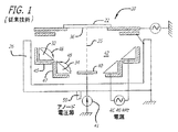
図1は、基板22上に付着物を形成するための、全体的に20で指示した、先行技術の装置の実施形態の一部分を簡単化した概略基本原理で示す。装置10は、接地シールド26から間隔を隔てられた一対のターゲット32及び34を含む。ターゲット32及び34の各々は、中空のせん頭円錐形状のような、適当な形状を備えるのがよい。ターゲット32及び34は、共通軸線35に同軸であるのがよく、ターゲット32は、ターゲット34から軸線方向にずらされ、かつ、ターゲット34より大きな直径を有する。ターゲット32及び34は、基板22の表面36上に層に付着される材料から作られるのがよい。例えば、銅の層を基板38上に付着する場合、ターゲット32及び34は、銅から作られるのがよい。しかしながら、ターゲット32は、ターゲット34の材料と異なる材料から作られてもよい。
Detailed Description of Preferred Embodiments of the Invention
FIG. 1 shows, in simplified schematic basic form, a portion of an embodiment of a prior art apparatus, indicated generally at 20, for forming deposits on a
アノード40が、ターゲット32及び34と間隔を隔てた、好ましくは、同軸の関係に配置される。正のバイアスが、電源41によってアノード40に印加されて、アノード40とターゲット32及び34の間に電界を生成じさせる。正のバイアスをアノード40に印加することは、プラズマの性質を変え、また、基板22の表面36上に付着した薄膜の特性について追加の制御を行うのに使用される。アノード40は、ターゲット32によりもターゲット34に近い。アノード40とターゲット32及び34は、キャビティを構成する。アノード40とターゲット32及び34の間の電界により、キャビティ42内に電子を生じさせる。磁石45及び47が、ターゲットの表面と平行な磁界48を生じさせるために、アノード32及び34に対してそれぞれ配置される。磁界48は、電界の方向と交差する方向に、好ましくは、磁化の方向と実質的に垂直な方向に配置される。
アルゴンのような不活性ガスの分子が、50のところで、キャビティ42の中へ導入される。これらの分子は、キャビティ42内の電子によってイオン化され、陽イオンを生じさせる。磁界と電界の間の交差関係、好ましくは実質的に垂直な関係の結果として、電子がキャビティ42内を螺旋進路で移動するので、キャビティ内のアルゴン分子のイオン化が促進される。アルゴンの陽イオンは、ターゲット32及び34まで移動し、ターゲットの傾斜面から、原子を放出させる。これらの原子は、基板22の露出面36に移動し、その露出面に付着することになる。
Inert gas molecules such as argon are introduced at 50 into the
AC電圧の二極の性質により、ターゲット32及び34の各々は、電圧の正の半サイクルがターゲットに印加されるとき、アノードとして作動し、一方、他方のターゲットは、カソードとして作動し、交流電圧の負の半サイクルでは、逆になる。二重マグネトロン装置が採用されるとき、重要な利点が達成される。二極モードでは、二つのターゲットは、放電のアノード及びカソードとして交互に働き、別のアノードを必要としない。しかしながら、二重カソードマグネトロン適用の領域は、薄膜付着中、基板が過熱されることになるため、及び、付着基板22上に配置された電子デバイスのあり得る照射損傷により、制限される。
Due to the bipolar nature of the AC voltage, each of the
中間周波数(例えば、40kHz)での放電の「パルス(pulsed)」特性により、プラズマは、電気信号の半周期ごとに点弧されなければならない。プラズマをターゲット付近に効果的に閉じ込めることができず、かくして、プラズマが、基板方向へも及ぶから、頻繁なプラズマ点弧(40kHz放電に対して、毎秒80000回)が、マグネトロンに、非平衡状態を作り出す。帯電粒子による過度の基板ボンバートは、成長薄膜の形成の構造的欠陥をもたらし、かつ、デバイスの損傷をもたらす。その上、ターゲットの一つが負の電位を有し、放電のカソードとして電子を放出するとき、もう一つのターゲットは、正の電位であり、電子を集める。しかし、強い磁界が、電子をターゲット表面から偏向させるから、正のターゲットは、電子の効果的なコレクターにはならない。その結果、付着工程中、著しい量の電子が、基板22の表面36に達し、それによって、基板に高温を発生させる。
Due to the “pulsed” nature of the discharge at an intermediate frequency (eg, 40 kHz), the plasma must be ignited every half cycle of the electrical signal. Since the plasma cannot be effectively confined in the vicinity of the target, and thus the plasma extends in the direction of the substrate, frequent plasma ignition (80,000 times per second for a 40 kHz discharge) is not balanced in the magnetron. To produce. Excessive substrate bombardment with charged particles results in structural defects in the formation of the grown thin film and device damage. Moreover, when one of the targets has a negative potential and emits electrons as a cathode for discharge, the other target is at a positive potential and collects electrons. However, since a strong magnetic field deflects electrons from the target surface, a positive target is not an effective collector of electrons. As a result, a significant amount of electrons reaches the
図10は、ターゲット32及び34への交流電圧の印加に応答して、装置20の作動を示す。交互の半サイクルでは、ターゲット32及び34の一方が、62のところで、スパッタリング状態にされることになり、64のところで、非活性化されることになる。
FIG. 10 illustrates the operation of the
上述した付着装置20には、未解決の問題がある。一つの問題は、ターゲット34から基板22の露出面に付着した材料の量が、ターゲット32から基板の表面に付着した材料の量より多いという事実から生じる。これは印加されるAC電力が対称であり、そのため、両方のターゲットが等しい量の電力を受けるが、ターゲットの幾何学的寸法及び位置が等しくないから起こる。この結果、基板の周囲におけるより、基板22の中央における付着速度がより高くなる。
There are unsolved problems with the
別の未解決の問題は、ターゲット34の表面上の電界から生ずる。電力の半サイクルでは、ターゲット34が、アノードとして作動するとき、ターゲット34は、電子を集める。しかし、ターゲット34の表面上の磁界が、ターゲットへの電子の流れに抵抗する。かくして、ターゲット34がアノードとして働くとき、ターゲット34の効率は低い。その結果、「コールド(cold)」電子が、基板22の表面36に達し、熱を発生させ、基板の表面上の成分を破壊することすらある。同じ問題が、ターゲット32がアノードとして働くとき、ターゲットに印加される交流電圧の他の半サイクルに存在する。
Another open problem arises from the electric field on the surface of the
この出願で開示され、請求され、且つ、図2及び図3に76で全体的に示された装置及び方法は、前の段落で説明した問題を解決する。本装置は、図1に示す、ターゲット32及び34と、アノード40と、を有する。しかしながら、交流電圧が、好ましくはほぼ20kHz乃至80kHzである中間範囲の周波数で、ターゲット32と34の間に印加される。
The apparatus and method disclosed, claimed in this application and generally indicated at 76 in FIGS. 2 and 3 solves the problems described in the previous paragraph. The apparatus includes
図9は、水平軸にそって連続的な周波数を示し、垂直軸に沿って、基板22上での、ターゲット32及び34からの材料の付着速度を示す、曲線74である。図9から分かるように、付着速度は、ゼロ周波数で1.0として指示された速度から徐々に減少し、周波数は、約20kHzから80kHzの中間範囲に徐々に増加する。
FIG. 9 is a
図9から分かるように、ターゲット32及びターゲット34に印加されるDC電圧について、付着速度は1.0である。交流電圧が、約40kHzの周波数でターゲット32とターゲット34の間に印加されるとき、付着速度は、約0.7の値まで減少する。交流電圧が、約80kHzの周波数でターゲット32とターゲット34の間に印加されるとき、付着速度は、約0.5の値まで減少する。
As can be seen from FIG. 9, for the DC voltage applied to the
図2は、本発明の好ましい実施形態の一つを構成する、76で全体的に指示した、装置を概略的に示す。装置は、ターゲット32及びターゲット34、キャビティ42、及び基板22を有する。図1中の磁石45及び47に相当する磁石45及び47が、装置に含まれるのがよい。シールド78、80及び82が、装置内に設けられ、接地のような適当な基準電位に電気的に接続されるのがよい。基板22は、電圧源83からのメガヘルツ範囲(例えば、13.66MHz)の無線周波数で交流電圧を受けるウエハーランド(waferland)84に配置されるのがよい。この段落で説明したような装置は、先行技術において知られている。
FIG. 2 schematically illustrates an apparatus, indicated generally at 76, that constitutes one of the preferred embodiments of the present invention. The apparatus has a
約20kHzから約80kHzの中間周波数範囲の交流電圧が、電圧源86によって提供される。電圧源86からの交流電圧の交互の半サイクルは、インダクタンス88を介してターゲット32に印加され、電圧源86からの他の半サイクルが、インダクタンス89を介してターゲット34に印加される。インダクタンス88及び89は、ローパスフィルタを構成し、かつ、交流電圧源86を、無線周波数(13.66MHz)の交流電圧を提供する交流電圧源92から隔離する。電圧源83及び92は、約13.66MHzのような、適当な無線周波数で作動する単一の電圧源に組み合わされるのがよい。
An alternating voltage in the intermediate frequency range of about 20 kHz to about 80 kHz is provided by
キャパシタ96及び97は、交流電圧源92と内側のターゲット34の間に、電圧源と外側のターゲット32の間に、それぞれ、接続される。ブロック形態に98で指示した非対称の回路は、その両端に、端子98a及び98bを有する。端子98a及び98bは、ローパスフィルタを構成し、かつ、非対称の回路を交流電圧源92によって提供されるRF電力から保護する、インダクタンス100及び102とキャパシタ140にそれぞれ接続される。
中間周波数(例えば、40kHz)の交流電圧は、電圧源86から、ターゲット32及び34に印加される。インダクタンス88及び89のインピーダンスが中間周波数で比較的低いから、電圧をターゲット32及び34に印加することができる。同時に、インダクタンス88及び89は、無線周波数(例えば、13.66MHz)で高いインピーダンスを有する。これにより、交流電圧源92からの電圧が交流電圧源86の作動に影響を及ぼすのを防止する。それはまた、交流電圧源92からの交流電圧が、ターゲット32及び34に加えられることを保障する。
An AC voltage having an intermediate frequency (for example, 40 kHz) is applied from the
キャパシタ96及び97はまた、交流電圧源92からターゲット32及び34に印加された無線周波数電力を分割する。分割の割合は、キャパシタ96及び97の相対値に依存する。無線周波数(13.66MHz)では、キャパシタ96及び97は、低いインピーダンスを有する。これにより、交流電圧源92からの電圧を、ターゲット32及び34に加えることができる。中間周波数では、キャパシタ96及び97は、高いインピーダンスを有する。これは、電圧源86からの電圧が、交流電圧源92に加えられるのを防止し、かつ、交流電圧源92からの電圧が、電圧源86に加えられるのを防止する。
電圧源86は、図11に100で示す交流電圧を生じさせる。交流電圧源92からの交流電圧は、電圧源86によって作り出された電圧100を変調する。この変調を、図11に102で示する。分かるように、電圧源86からの電圧の振幅は、交流電圧源92からの電圧の振幅よりもかなり大きい。先行技術におけるように、電圧電圧源86だけが設けられたならば、正のトリガ電圧70を、図11に示したように、交流電圧の交互の半サイクルでターゲット32に生じさせる。同様に、正のトリガ電圧76を、図11に示したように、交流電圧の他の半サイクルでターゲット34に生じさせる。
The
中間周波数(40kHz)の交流電圧を無線周波数(例えば13.66MHz)の交流電圧で変調することによって、電圧源86からの交流電圧の最初の半サイクルでのみトリガ信号を生じさせる。これを、図12に108で示す。引き続く交互の半サイクルのいずれにおいても、トリガ信号108に対応する非トリガ信号を生じさせない。これは、円滑な付着が、ターゲット32から基板22に行われることを保証する。同様に、正の電圧がターゲット34に加えられるとき、トリガ信号108に対応する単一のトリガ信号だけを、半サイクルの最初の一つで、ターゲット34に生じさせる。その後、トリガ信号を、ターゲット34に生じさせない。これは、先行技術で(電圧源86に対応する)ソースからの交流電圧の各半サイクルでプラズマ放電に作られる異物の、基板22上でのいかなる付着をも除去する。
By modulating an alternating voltage at an intermediate frequency (40 kHz) with an alternating voltage at a radio frequency (eg, 13.66 MHz), a trigger signal is generated only in the first half cycle of the alternating voltage from the
電圧源86からの交流電圧が、交流電圧源92からの交流電圧によって変調されるときも、基板の中央領域におけるターゲットからの材料の付着速度は、基板の周囲におけるターゲット32からの材料の付着速度より大きい。これは、何が先行技術において起きるかである。各事例において、劣悪な品質の基板が作り出される。
Even when the AC voltage from
図2に示す本装置72は、基板の中央部分と周辺部分での基板22の厚さの違いを補償する。これは、非対称回路98を設けることによって達成される。非対称回路98は、その両端に、端子98a及び98bを有する。非対称回路98は、ターゲット34によりもターゲット32にもっと電力を与えて、ターゲットによって基板に生じさせる付着速度を等しくする。これは、交流電圧110がターゲット34に加えられ、かつ、交流電圧112がターゲット32に加えられる場合、図8から分かる。交流電圧110及び112は、軸線114に対して配置される。普通は、先行技術におけるように、交流電圧は、交流電圧110及び112のピーク間の中間の軸線115に対して配置される。
The apparatus 72 shown in FIG. 2 compensates for the difference in thickness of the
図8に示すように、ターゲット32に加えられた交流電圧112の大きさは、軸線が図8の114にあるとき、ターゲット34に加えられる電圧110の大きさより大きい。これは、基板22にターゲット32から与えられる付着の速度を増加させ、かつ、基板にターゲット34から与えられる付着の速度を減少させる。ターゲット32及び34に印加される電圧の相対振幅を、基板の全ての位置における付着速度が実質的に均一であるように調節することができる。その結果、基板22上の付着物の厚さは、基板の全ての位置で実質的に均一である。
As shown in FIG. 8, the magnitude of the alternating voltage 112 applied to the
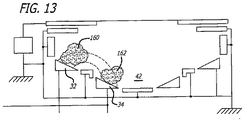
図3は、非対称回路98の端子の個々の一つから、アノード40に、及び、プロセスチャンバー内の(シールド78及び80を含む)他のシールドに各々接続された二つの追加のダイオード202及び203を示す。上述したように、磁界は、「コールド(cold)」電子が、図13のプラズマ160及び162を出ることを妨げる。その結果、これらの電子は、先行技術では、基板22に移動し、基板に移動するイオンによって、基板の熱を作り、基板のボンバートを生じさせる。この熱及びボンバートは、先行技術の装置では基板上のデバイス(チップ)を損傷させる。
FIG. 3 shows two
この発明の装置にダイオード202及び203を含めることによって、「コールド(cold)」電子は、先行技術より遙かに容易に、プラズマ160及び102を出て、シールド(例えば78及び80)に移動する。例えば、電圧の負の半サイクルが、ターゲット32に印加されると仮定する。この場合、ダイオード202は、高いインピーダンスを有する。非対称回路98の反対側の端子は、この時、正の電位を有する。これにより、ダイオード203は、低インピーダンスを有し、非対称回路98から正の電圧をターゲット34、アノード40及びシールド78及び80に印加させる。プラズマ162を出るために、「コールド(cold)」電子は、ターゲット34をパスし、かつ、シールド78及び80及びアノード40をパスしなければならない。最も好ましいパスは、シールド80及び78、及びアノード40を通ることである、というのは、プロセスチャンバーのこれらの構成要素は、電子に対して低抵抗を有し、ターゲット34がその表面に、電子がターゲット34に達するのを抑制する磁界を有するからである。その結果、「コールド(cold)」電子は、プラズマ放電162を出て、アノード40及びシールド(例えば、78及び80)に通り、電子のエネルギーを、基板22、又はプロセスチャンバーの他の部分の熱として放散しない。負の電圧がターゲット34に印加されるとき、回路は、先の段落で説明したのと同じように働くが、正の電圧は、今や、ダイオード202を介して印加される。同時に、ダイオード203は、高インピーダンスを有する。
By including
「コールド(cold)」電子が基板22に通るのを防止することは、基板の温度を減じ、典型的には、数百MPaの高圧縮応力を有する酸化物フィルム及び窒化物フィルムの圧縮応力を減ずる。
Preventing “cold” electrons from passing through the
図5は、図3に示す非対称発生器98の、全体的に120で示した、好ましい実施形態を、簡単化した基本原理で示す。実施形態120は、非対称回路98の両端に、端子98a及び98bを有する。実施形態120はまた、概略的な基本原理で、中間周波数(例えば、40kHz)の交流電圧を、非対称回路98に加えるための交流電源86を有する。 キャパシタ122及びダイオード124は、互いに並列であり、端子98aと端子98bとの間で、電圧源86と直列である。
FIG. 5 shows, in simplified basic principle, a preferred embodiment, generally designated 120, of the
ダイオード124の順方向では、ダイオードは、低インピーダンスを有する。交互の半サイクルで、電流が、電圧源86からダイオード124を通ってターゲット32に流れる。これは、図8に112で示す大きな信号を生じさせる。電圧源86からの交流電圧の他の半サイクルでは、ダイオード124は高インピーダンスを有し、電流の流れを阻止する。しかしながら、電流は、キャパシタ122を通って流れるが、その流れは、キャパシタの大きさに依存する量によって制限される。これにより、作り出されるべき図8中の交流電流信号110を生じさせる。
In the forward direction of the
キャパシタ122は、ターゲット34に印加される電圧の振幅が、図8に110で示したようであるように選択される。図8の交流電圧110及び112のピーク振幅の間の差は、キャパシタ122の大きさとに依存し、かつ、電圧源86によって与えられる交流電圧の周波数に依存する。この差は、基板22上に、ターゲット32及び34によって与えられる付着物の厚さの差を保証するように選択される。
図6は、図2及び図3の非対称回路98の、全体的に130で示す、別の好ましい実施形態を、概略的な基本原理で示す。実施形態130は、図5にも示す、ダイオード124及びキャパシタ122を有する。実施形態130はまた、(a)電圧源86の両端に接続された一次巻線132と、(b)一次巻線132と磁気的に結合した二次巻線134と、を有する。二次巻線134の一方の端子は、端子98bに接続され、二次巻線の他方の端子は、キャパシタ122及びダイオード124に接続される。
FIG. 6 illustrates, in schematic basic principles, another preferred embodiment, generally designated 130, of the
電流が、電圧源86からの交流電圧の半サイクル毎にで、一次巻線132に流れる。交互の半サイクルでは、ターゲット32が、基板22上に付着物を形成するとき、電流が、ダイオード124によって与えられた低インピーダンスパスを通って流れる。これにより、巻線132と巻線134の間の磁気構造に蓄積されたエネルギーの全てをダイオード124を通して分配する。しかしながら、電圧源86からの交流電圧の別の半サイクルでは、ダイオード124は高インピーダンスを有し、一次巻線によってもたらされるエネルギーの一部分だけが、キャパシタ22を通る電流によって分配される。これにより、エネルギーのいくらかを、巻線の間の磁気構造にとどめさせる。このエネルギーは、交流電圧の次に半サイクルで、ダイオード124を通る電流の流れによって分配される。これにより、図8の電圧112のピーク振幅を、電圧110のピーク振幅に対して増加させる。
Current flows through the primary winding 132 every half cycle of the AC voltage from the
図7は、図2及び図3における非対称回路98の、全体的に136で示す、他の好ましい実施形態を概略的な基本原理で示す。この実施形態では、電圧源138からの直流電圧が、端子98aと端子98bの間に印加される。直流電圧は、図8の電圧112のピーク振幅を増加させ、かつ、電圧110のピーク振幅を減少させる方向に印加される。電圧112のピーク振幅の増加量、及び、電圧110のピーク振幅の減少量は、電圧源138によって与えられる流電圧の振幅に依存する。
FIG. 7 shows, in schematic basic principles, another preferred embodiment, generally designated 136, of the
図4は、図2及び図3にも示す回路の部分を示す。図4に示す回路部分は、非対称回路98、ターゲット32及び34、及びインダクタンス100及び102を含む。回路のこの部分は、インダクタンス100及び102が、交流電源92からの約13.66MHzの無線周波数エネルギーが非対称回路98を通るのを防止するフィルタとして作用する。
FIG. 4 shows the portion of the circuit also shown in FIGS. The circuit portion shown in FIG. 4 includes an
先に示したように、誘電体材料が、付着装置76内のターゲット32及び34、及び、その他の構成要素の表面に蓄積する。酸素、窒素及びメタンのようなガスの分子が、ターゲット32及び34の表面から放出された分子又は原子と反応するとき、誘電体層が蓄積する。放出された原子又は分子は、例示として、シリコン、アルミニウム又はタンタルであり、それらは、例示として、酸素、窒素及びメタン分子と反応して、例示として、二酸化珪素、酸化アルミニウム、酸素と窒素を含むタンタル化合物を形成する。これらの化合物は、ターゲット32及び34の表面に付着し、ターゲット32及び34を形成する材料の原子又は分子が、ターゲットから放出されないようにする。
As indicated above, dielectric material accumulates on the surfaces of
前段落で説明した誘電体材料のうちの一つの層が、ターゲット32に付着されたと仮定する。また、ターゲット32が、電圧源86から負の電圧を受けていると仮定する。このとき、正のイオンから形成されたプラズマ160が、ターゲット32に隣接してキャビティ42内に蓄積されている。プラズマ160を、図13に雲として示す。プラズマ160は、負のターゲット32に隣接して形成される、というのは、プラズマは比較的ゆっくりと移動する正のイオンから作られ、プラズマがターゲットに隣接して蓄積するからである。
Assume that one layer of the dielectric material described in the previous paragraph has been deposited on the
ターゲット32に隣接して正のイオンによって形成されたプラズマ160は、比較的強く、ターゲット32の表面に付着された誘電体材料の層は、比較的薄い。その結果、電界が、プラズマ160からのイオンを加速し、ターゲット32のボンバートを生じさせる。ボンバートにより、ターゲット34の表面の誘電体材料を、ターゲットから除去させる。このようにして、ターゲット32及び34の表面は、電圧源86からの交流電圧の次々の半サイクルで、誘電体材料が交互に掃除される。
The
誘電体材料がターゲット32の表面から除去される半サイクル中、上述したように、誘電体材料の層がターゲット34に形成される。電圧源86からの交流電圧の次の半サイクルでは、誘電体層は、上述した方法で、プラズマ162の作用によって、ターゲット34の表面から除去される。このように、ターゲット32及び34の表面は、電圧源86からの交流電圧の次々の半サイクルで、誘電体材料が交互に掃除される。
During the half cycle in which the dielectric material is removed from the surface of the
この発明は、特定の実施形態を参照して、説明し、図示したが、含まれる原理は、当業者にとって明らかな他の多数の実施形態に使用することができる。したがって、本発明は、添付の特許請求の範囲によって指示されるようにのみ限定されるべきである。 Although the invention has been described and illustrated with reference to specific embodiments, the principles involved can be used in many other embodiments that will be apparent to those skilled in the art. Accordingly, the invention should be limited only as indicated by the appended claims.
Claims (18)
第1ターゲットと、
前記第1ターゲットからずらされ、かつ、前記第1ターゲットと同軸関係に配置された第2ターゲットと、
交流電圧を第1周波数で前記第1及び第2ターゲットに与える、前記第1及び第2ターゲットに作動的に接続された第1電気回路と、
前記基板上に前記第1及び第2ターゲットから付着される材料の相対量を調節して、前記基板の表面に実質的に均一な付着物を形成するために、前記第1及び第2ターゲットに印加される交流電圧を調節する、前記第1電気回路と作動的に関連した第2電気回路と、の組合せであって、
前記第1電気回路は、前記第1及び第2ターゲットに印加するための対称の交流電圧を提供し、
前記第2電気回路は、前記基板上の、前記第1及び第2ターゲットからの付着の速度の差を補償するために、ターゲットの一方に、ターゲットの他方におけるよりも交流電圧の大きい振幅を与える、組合せ。 A combination for use with a substrate,
A first target;
A second target displaced from the first target and arranged in a coaxial relationship with the first target;
A first electrical circuit operatively connected to the first and second targets for applying an alternating voltage to the first and second targets at a first frequency;
Adjusting the relative amount of material deposited on the substrate from the first and second targets to form a substantially uniform deposit on the surface of the substrate to the first and second targets. A combination of a second electrical circuit operatively associated with the first electrical circuit that regulates an applied alternating voltage;
The first electrical circuit provides a symmetrical alternating voltage for application to the first and second targets;
The second electrical circuit provides one of the targets with a greater amplitude of the AC voltage than on the other of the targets to compensate for the difference in the rate of deposition from the first and second targets on the substrate. ,combination.
第1ターゲットと、
第1ターゲットと間隔を隔てたせん頭円錐形の関係に配置された第2ターゲットと、
第1ターゲットと第2ターゲットとの間に、中間の周波数範囲内の特定周波数の交流電圧を印加するための第1電気回路と、
前記基板上に前記第1及び第2ターゲットから付着される材料の相対量を調節して、前記基板の表面上に前記第1及び第2ターゲットから材料の付着物を前記基板の前記表面の全体にわたって実質的に均一な厚さに形成するために、第1及び第2ターゲットへの特定周波数の電力の印加を調節するための前記第1電気回路と作動的に関連した第2電気回路と、
無線周波数の交流電圧信号で、特定周波数の信号を変調するための第3電気回路と、
の組合せであって、
前記第1及び第2ターゲットは、前記第1ターゲットからの前記基板上の材料の、前記第2ターゲットからよりも、大きい付着速度をもたらすように、前記基板に対して配置され、
前記第2電気回路の調節は、特定周波数の交流電圧を、前記第1及び第2ターゲットからの前記基板上の材料の付着速度の差を補償するために、前記第1ターゲットに印加されるよりも大きい振幅で前記第2ターゲットに印加することを含む、組合せ。 A combination for depositing material on a substrate,
A first target;
A second target arranged in a frustoconical relationship spaced from the first target;
A first electric circuit for applying an alternating voltage of a specific frequency within an intermediate frequency range between the first target and the second target;
The relative amount of material deposited from the first and second targets on the substrate is adjusted to deposit material deposits from the first and second targets on the surface of the substrate over the entire surface of the substrate. A second electrical circuit operatively associated with the first electrical circuit for adjusting the application of power at a particular frequency to the first and second targets to form a substantially uniform thickness over the first and second targets;
A third electrical circuit for modulating a signal of a specific frequency with a radio frequency AC voltage signal;
A combination of
The first and second targets are positioned relative to the substrate to provide a higher deposition rate of material on the substrate from the first target than from the second target;
The adjustment of the second electrical circuit is such that an alternating voltage of a specific frequency is applied to the first target to compensate for the difference in the deposition rate of the material on the substrate from the first and second targets. And applying to the second target with a greater amplitude.
請求項2記載の組合せ。 The specific frequency is in a range of 20 kHz to 80 kHz.
The combination according to claim 2.
前記第2電気回路は、交流電圧の負の半サイクルで、特定周波数の交流電圧を前記第2ターゲットに通すために、前記ダイオードの両端に接続されたキャパシタを更に含む、
請求項2記載の組合せ。 The second electrical circuit passes an AC voltage of a specific frequency through the second target in a positive half cycle of an AC voltage, and an AC of a specific frequency to the first target in a negative half cycle of the AC voltage. Including a diode connected to block the passage of voltage;
The second electrical circuit further includes a capacitor connected across the diode to pass an AC voltage of a specific frequency through the second target in a negative half cycle of an AC voltage.
The combination according to claim 2.
請求項2記載の組合せ。 The second electric circuit stores energy in a negative half cycle of an AC voltage having a specific frequency, and releases the stored energy to the first target in a positive half cycle of the AC voltage having a specific frequency. Including transformers connected in the circuit, such as
The combination according to claim 2.
各々互いに同軸関係に配置され、かつ、前記基板上に材料を付着させるために前記基板に対して配置された第1及び第2ターゲットと、
反対極の交流電圧を前記第1及び第2ターゲットにそれぞれ加えるための、前記第1及び第2ターゲットに接続された交流電圧源と、
前記第1及び第2ターゲットに印加される交流電圧に非対称を与える、交流電圧源、及び前記第1及び第2ターゲットに接続された電気回路と、の組合せであって、
この非対称は、前記基板の表面に実質的に均一な付着物を形成する方向にあり、前記電気回路は、ターゲットの一方からの前記基板上の材料の高い付着速度を、他方のターゲットからの前記基板上の材料の付着速度に対して、補償するために、交流電圧の交互の半サイクルで、ターゲットの一方に、他の半サイクルで、ターゲットの他方に加えられた交流電圧の振幅に対して、限定された振幅の電圧を加える、組合せ。 A combination for use with a substrate,
First and second targets, each disposed coaxially with each other and disposed with respect to the substrate to deposit material on the substrate;
An AC voltage source connected to the first and second targets for applying opposite polarity AC voltages to the first and second targets, respectively;
A combination of an alternating voltage source that provides asymmetry to the alternating voltage applied to the first and second targets, and an electrical circuit connected to the first and second targets,
This asymmetry is in the direction of forming a substantially uniform deposit on the surface of the substrate, and the electrical circuit causes a high deposition rate of material on the substrate from one of the targets to increase the deposition rate from the other target. To compensate for the deposition rate of the material on the substrate, in alternating half cycles of alternating voltage, on one side of the target, on the other half cycle, on the other side of the target Apply a limited amplitude voltage, combination.
請求項7記載の組合せ。 The electric circuit is connected to both ends of the AC voltage source, and in the other half cycle, the amplitude of the voltage applied to one of the first and second targets in alternate half cycles of the AC voltage is determined in the other half cycle. A DC voltage source connected to the first and second targets to limit the amplitude of the AC voltage applied to the other of the first and second targets;
The combination according to claim 7.
(a)交流電圧の交互の半サイクルで前記第1及び第2ターゲットの一方に加えられる交流電圧を、交流電圧の他方の半サイクルで、前記第1及び第2ターゲットの他方に加えられる交流電圧の振幅に対して、制限する、ダイオード及び、前記ダイオードの両端に接続されたキャパシタ、
(b)一次巻線及び二次巻線を備え、前記一次巻線は、交流電圧源に接続され、前記二次巻線は、前記電気回路に含まれ、交流電圧の交互の半サイクルで、前記第1及び第2ターゲットの一方に加えられる電圧の振幅を、他方の半サイクルで、前記第1及び第2ターゲットの他方に加えられる交流電圧の振幅に対して、制限する際に、前記ダイオード及び前記キャパシタと協同する変圧器、及び、
(c)前記交流電圧源に接続され、かつ、前記第1及び第2ターゲットに接続され、交流電圧の交互の半サイクルで、前記第1及び第2ターゲットの一方に加えられる電圧の振幅を、交流電圧の他方の半サイクルで、前記第1及び第2ターゲットの他方に加えられる交流電圧の振幅に対して、制限する直流電圧源、
の一つを含む、請求項7記載の組合せ。 The electrical circuit is
(A) An alternating voltage applied to one of the first and second targets in alternating half cycles of alternating voltage, and an alternating voltage applied to the other of the first and second targets in the other half cycle of alternating voltage. A diode, and a capacitor connected across the diode, for limiting the amplitude of
(B) comprising a primary winding and a secondary winding, wherein the primary winding is connected to an AC voltage source, the secondary winding is included in the electrical circuit, and in alternating half cycles of the AC voltage; In limiting the amplitude of the voltage applied to one of the first and second targets to the amplitude of the alternating voltage applied to the other of the first and second targets in the other half cycle, the diode And a transformer cooperating with the capacitor, and
(C) connected to the AC voltage source and connected to the first and second targets, and the amplitude of the voltage applied to one of the first and second targets in alternating half cycles of the AC voltage, A DC voltage source that limits the amplitude of the AC voltage applied to the other of the first and second targets in the other half cycle of the AC voltage;
8. The combination of claim 7, comprising one of the following:
前記基板上に、一対のターゲットの表面からの材料を付着させるために、前記一対のターゲットを同軸関係に配置するステップと、
非対称の特性を有する交流電圧を与えて、前記基板上の異なる位置での前記一対のターゲットからの材料の付着速度の差を補償するステップと、
前記基板上の、前記一対のターゲットからの材料の付着速度において、非対称交流電圧をターゲットに加えて、基板表面上の異なる位置での第1及び第2ターゲットからの材料の付着速度の差を補償するステップと、の方法であって、
交流電圧の非対称により、交流電圧の交互の半サイクルで前記一対のターゲットの一方に印加される交流電圧の振幅を、交流電圧の他の半サイクルで前記一対のターゲットの他方に印加された交流電圧の振幅と異ならせて、前記基板上の異なる位置での、前記一対のターゲットの各々からの材料の付着速度の差を補償する、方法。 A method of forming a deposit on a substrate,
Arranging the pair of targets in a coaxial relationship to deposit material from the surface of the pair of targets on the substrate;
Providing an alternating voltage having an asymmetric characteristic to compensate for differences in material deposition rates from the pair of targets at different locations on the substrate;
At the deposition rate of material from the pair of targets on the substrate, an asymmetrical alternating voltage is applied to the target to compensate for the difference in deposition rate of material from the first and second targets at different locations on the substrate surface. And a step of:
Due to the asymmetry of the alternating voltage, the amplitude of the alternating voltage applied to one of the pair of targets in alternating half cycles of the alternating voltage, and the alternating voltage applied to the other of the pair of targets in the other half cycle of the alternating voltage. Different from the amplitude of the substrate to compensate for differences in the deposition rate of material from each of the pair of targets at different locations on the substrate.
請求項10記載の方法。 The alternating voltage has a first frequency, and an alternating voltage having a second frequency higher than the first frequency modulates the alternating voltage at the first frequency, and in the first cycle of the alternating voltage at the first frequency. Only triggering each of the pair of targets.
The method of claim 10.
請求項11記載の方法。 The alternating voltage having the first frequency has an intermediate frequency in the range of 20 kilohertz (20 kHz) to 80 kilohertz (80 kHz), and the alternating voltage having the second frequency has a frequency in the radio frequency range. Yes,
The method of claim 11.
電界を、前記キャビティ内で、第1の方向に、前記アノードと前記一対のターゲットの間に生じさせ、
磁界を、前記キャビティ内で、第1の方向と実質的に垂直な第2の方向に生じさせる、請求項10記載の方法。 An anode is disposed with respect to the pair of targets to form a cavity together with the pair of targets,
An electric field is generated in the cavity in the first direction between the anode and the pair of targets;
The method of claim 10, wherein a magnetic field is generated in the cavity in a second direction substantially perpendicular to the first direction.
交流電圧は第1周波数を有し、前記第1周波数より高い第2周波数を有する交流電圧が、前記第1周波数の交流電圧を変調して、前記第1周波数でターゲットに印加される交流電圧の最初の一サイクルでのみ、前記一対のターゲットの各々のトリガリング(triggering)を行わせる、請求項10記載の方法。 Due to the asymmetry of the AC voltage, the amplitude of the AC voltage applied to one of the pair of targets in alternating half cycles of the AC voltage, and the AC voltage applied to the other of the pair of targets in the other half cycle of the AC voltage. To compensate for the difference in the deposition rate of the material from each of the pair of targets at different locations on the substrate,
The AC voltage has a first frequency, and an AC voltage having a second frequency higher than the first frequency modulates the AC voltage of the first frequency and is applied to the target at the first frequency. The method according to claim 10, wherein triggering of each of the pair of targets is performed only in the first cycle.
前記基板上に一対のターゲットの表面から材料を付着させるために、前記一対のターゲットを同軸関係に配置するステップと、
前記一対のターゲットの間に、第1周波数を有する第1交流電圧を印加して、交流電圧の交互の半サイクルで前記基板上に一方のターゲットからの材料の付着物を得、交流電圧の他の半サイクルで前記基板上に他方のターゲットからの材料の付着物を得るステップであって、前記基板上の、前記一方のターゲットからの材料の付着速度に対する、前記基板上の、前記他方のターゲットからの材料の付着速度の差を補償するために、前記交互の半サイクルでの前記第1交流電圧の振幅が、他の半サイクルでの前記第1交流電圧の振幅より大きいステップと、
前記第1周波数でターゲットに印加される交流電圧の最初の一つのサイクルでのみ、前記一対のターゲットの各々のトリガリング(triggering)を行わせるように、前記第1周波数より高い第2周波数を有する第2交流電圧で、前記第1交流電圧を変調するステップと、の方法。 A method of forming a deposit on a substrate,
Arranging the pair of targets in a coaxial relationship to deposit material from the surface of the pair of targets on the substrate;
A first AC voltage having a first frequency is applied between the pair of targets to obtain a deposit of material from one target on the substrate in alternating half cycles of the AC voltage. Obtaining a deposit of material from the other target on the substrate in a half cycle of the other target on the substrate relative to the deposition rate of the material from the one target on the substrate. The amplitude of the first AC voltage in the alternate half cycle is greater than the amplitude of the first AC voltage in the other half cycle to compensate for the difference in material deposition rate from
Having a second frequency higher than the first frequency so as to trigger each of the pair of targets only in the first cycle of an alternating voltage applied to the target at the first frequency. Modulating the first AC voltage with a second AC voltage.
前記第2周波数は、メガヘルツの範囲内の無線周波数である、
請求項15記載の方法。 The first frequency is between 20 kHz and 80 kHz;
The second frequency is a radio frequency in the megahertz range;
The method of claim 15.
請求項15記載の方法。 The difference between the amplitude of the second AC voltage in the alternate half cycle and the amplitude of the second AC voltage in the other half cycle is the difference between the second AC voltage and the capacitor of the first value in the alternate half cycle. And by passing the second alternating voltage through a second value capacitor different from the first value in another half cycle,
The method of claim 15.
請求項15記載の方法。 The first frequency is 20 kilohertz (20 kHz) to 80 kilohertz (80 kHz), and the second frequency is 13.66 megahertz (13.66 MHz).
The method of claim 15.
Applications Claiming Priority (3)
| Application Number | Priority Date | Filing Date | Title |
|---|---|---|---|
| US10/446,005 | 2003-05-23 | ||
| US10/446,005 US7179350B2 (en) | 2003-05-23 | 2003-05-23 | Reactive sputtering of silicon nitride films by RF supported DC magnetron |
| PCT/US2004/015115 WO2004107411A2 (en) | 2003-05-23 | 2004-05-12 | Deposition apparatus and method |
Publications (3)
| Publication Number | Publication Date |
|---|---|
| JP2007501333A JP2007501333A (en) | 2007-01-25 |
| JP2007501333A5 JP2007501333A5 (en) | 2007-08-02 |
| JP5324744B2 true JP5324744B2 (en) | 2013-10-23 |
Family
ID=33450968
Family Applications (1)
| Application Number | Title | Priority Date | Filing Date |
|---|---|---|---|
| JP2006533061A Expired - Fee Related JP5324744B2 (en) | 2003-05-23 | 2004-05-12 | Adhesion apparatus and method |
Country Status (5)
| Country | Link |
|---|---|
| US (1) | US7179350B2 (en) |
| EP (1) | EP1634317A2 (en) |
| JP (1) | JP5324744B2 (en) |
| TW (1) | TW200502426A (en) |
| WO (1) | WO2004107411A2 (en) |
Families Citing this family (13)
| Publication number | Priority date | Publication date | Assignee | Title |
|---|---|---|---|---|
| US7758982B2 (en) * | 2005-09-02 | 2010-07-20 | Hitachi Global Storage Technologies Netherlands B.V. | SiN overcoat for perpendicular magnetic recording media |
| US7517437B2 (en) * | 2006-03-29 | 2009-04-14 | Applied Materials, Inc. | RF powered target for increasing deposition uniformity in sputtering systems |
| US20080083611A1 (en) * | 2006-10-06 | 2008-04-10 | Tegal Corporation | High-adhesive backside metallization |
| US20090246385A1 (en) * | 2008-03-25 | 2009-10-01 | Tegal Corporation | Control of crystal orientation and stress in sputter deposited thin films |
| US8691057B2 (en) * | 2008-03-25 | 2014-04-08 | Oem Group | Stress adjustment in reactive sputtering |
| US8482375B2 (en) * | 2009-05-24 | 2013-07-09 | Oem Group, Inc. | Sputter deposition of cermet resistor films with low temperature coefficient of resistance |
| GB2473655A (en) * | 2009-09-21 | 2011-03-23 | Mantis Deposition Ltd | Magnetron sputtering techiques and apparatus |
| WO2012095961A1 (en) * | 2011-01-12 | 2012-07-19 | 日新電機株式会社 | Plasma apparatus |
| US20170178878A1 (en) | 2015-12-21 | 2017-06-22 | IonQuest LLC | Electrically and Magnetically Enhanced Ionized Physical Vapor Deposition Unbalanced Sputtering Source |
| US11359274B2 (en) | 2015-12-21 | 2022-06-14 | IonQuestCorp. | Electrically and magnetically enhanced ionized physical vapor deposition unbalanced sputtering source |
| US11823859B2 (en) * | 2016-09-09 | 2023-11-21 | Ionquest Corp. | Sputtering a layer on a substrate using a high-energy density plasma magnetron |
| US20210230739A1 (en) * | 2020-01-27 | 2021-07-29 | Applied Materials, Inc. | Physical Vapor Deposition Apparatus And Methods With Gradient Thickness Target |
| CN116155231A (en) * | 2023-02-28 | 2023-05-23 | 苏州敏声新技术有限公司 | Bulk acoustic wave resonator and preparation method thereof |
Family Cites Families (11)
| Publication number | Priority date | Publication date | Assignee | Title |
|---|---|---|---|---|
| JPS63230872A (en) * | 1984-05-17 | 1988-09-27 | バリアン・アソシエイツ・インコ−ポレイテツド | target and magnetically enhanced R. F. Magnetron sputter device with separate limiting magnetic field to separate bias |
| US4661228A (en) * | 1984-05-17 | 1987-04-28 | Varian Associates, Inc. | Apparatus and method for manufacturing planarized aluminum films |
| JPH01116068A (en) * | 1987-10-28 | 1989-05-09 | Hitachi Ltd | Bias sputtering device |
| US4810347A (en) | 1988-03-21 | 1989-03-07 | Eaton Corporation | Penning type cathode for sputter coating |
| JPH02225662A (en) * | 1989-02-27 | 1990-09-07 | Tokuda Seisakusho Ltd | Sputtering device |
| DE4127262C1 (en) | 1991-08-17 | 1992-06-04 | Forschungsges Elektronenstrahl | Sputtering equipment for coating large substrates with (non)ferromagnetic material - consisting of two sub-targets electrically isolated and cooling plates whose gap in between is that in region of pole units |
| US5415757A (en) * | 1991-11-26 | 1995-05-16 | Leybold Aktiengesellschaft | Apparatus for coating a substrate with electrically nonconductive coatings |
| DE19848636C2 (en) * | 1998-10-22 | 2001-07-26 | Fraunhofer Ges Forschung | Method for monitoring an AC voltage discharge on a double electrode |
| JP2001003166A (en) | 1999-04-23 | 2001-01-09 | Nippon Sheet Glass Co Ltd | Method for coating surface of substrate with coating film and substrate by using the method |
| EP1235947A4 (en) | 1999-10-15 | 2009-04-15 | Advanced Energy Ind Inc | Method and apparatus for substrate biasing in multiple electrode sputtering systems |
| US6824653B2 (en) * | 2003-02-21 | 2004-11-30 | Agilent Technologies, Inc | Magnetron with controlled DC power |
-
2003
- 2003-05-23 US US10/446,005 patent/US7179350B2/en active Active - Reinstated
-
2004
- 2004-05-12 EP EP04752195A patent/EP1634317A2/en not_active Withdrawn
- 2004-05-12 WO PCT/US2004/015115 patent/WO2004107411A2/en active Application Filing
- 2004-05-12 JP JP2006533061A patent/JP5324744B2/en not_active Expired - Fee Related
- 2004-05-20 TW TW093114246A patent/TW200502426A/en unknown
Also Published As
| Publication number | Publication date |
|---|---|
| JP2007501333A (en) | 2007-01-25 |
| EP1634317A2 (en) | 2006-03-15 |
| WO2004107411A2 (en) | 2004-12-09 |
| US7179350B2 (en) | 2007-02-20 |
| WO2004107411A3 (en) | 2005-12-29 |
| US20040231972A1 (en) | 2004-11-25 |
| TW200502426A (en) | 2005-01-16 |
Similar Documents
| Publication | Publication Date | Title |
|---|---|---|
| US20190368030A1 (en) | Apparatus for generating high-current electrical discharges | |
| JP4461253B2 (en) | Plasma generation method | |
| KR100485034B1 (en) | Plasma processing system and method | |
| JP6042048B2 (en) | High power pulsed magnetron sputtering method and high power electrical energy source | |
| KR100372385B1 (en) | Thin film fabrication method and thin film fabrication apparatus | |
| JP5324744B2 (en) | Adhesion apparatus and method | |
| US20070034498A1 (en) | Pulsed magnetron sputtering deposition with preionization | |
| KR20010040132A (en) | A plasma processing system and a method of depositing material on a substrate | |
| JPH02298024A (en) | Reactive ion etching apparatus | |
| JP2009057637A (en) | Ionized physical vapor deposition apparatus using helical magnetic resonance coil | |
| JPH07188917A (en) | Collimation device | |
| WO2002037529A2 (en) | Pulsed sputtering with a small rotating magnetron | |
| JP2010512458A (en) | RF substrate bias using high power impulse magnetron sputtering (HIPIMS) | |
| JPH06212421A (en) | Device for coating substrate | |
| JP2001279436A (en) | Method and apparatus for physical growing of deposited film in vapor phase using modulated power source | |
| JP4588212B2 (en) | Sputtering apparatus comprising a coil having overlapping ends | |
| JP3319285B2 (en) | Plasma processing apparatus and plasma processing method | |
| US20080286496A1 (en) | Method for depositing electrically insulating layers | |
| JP2005248322A (en) | Process for depositing composite coating on surface | |
| JP2007501333A5 (en) | ||
| US6471831B2 (en) | Apparatus and method for improving film uniformity in a physical vapor deposition system | |
| JP2001512887A (en) | Modulated power for ionized metal plasma deposition | |
| KR100641956B1 (en) | Sputter target for physical vapor deposition | |
| JPH06502892A (en) | Method for carrying out sputter coating treatment and sputter coating apparatus | |
| KR20180019201A (en) | Vacuum arc deposition apparatus and deposition method |
Legal Events
| Date | Code | Title | Description |
|---|---|---|---|
| A521 | Request for written amendment filed |
Free format text: JAPANESE INTERMEDIATE CODE: A523 Effective date: 20070514 |
|
| A621 | Written request for application examination |
Free format text: JAPANESE INTERMEDIATE CODE: A621 Effective date: 20070514 |
|
| A131 | Notification of reasons for refusal |
Free format text: JAPANESE INTERMEDIATE CODE: A131 Effective date: 20100906 |
|
| A601 | Written request for extension of time |
Free format text: JAPANESE INTERMEDIATE CODE: A601 Effective date: 20101206 |
|
| A602 | Written permission of extension of time |
Free format text: JAPANESE INTERMEDIATE CODE: A602 Effective date: 20101213 |
|
| A521 | Request for written amendment filed |
Free format text: JAPANESE INTERMEDIATE CODE: A523 Effective date: 20110307 |
|
| A131 | Notification of reasons for refusal |
Free format text: JAPANESE INTERMEDIATE CODE: A131 Effective date: 20110627 |
|
| A601 | Written request for extension of time |
Free format text: JAPANESE INTERMEDIATE CODE: A601 Effective date: 20110927 |
|
| A602 | Written permission of extension of time |
Free format text: JAPANESE INTERMEDIATE CODE: A602 Effective date: 20111004 |
|
| A521 | Request for written amendment filed |
Free format text: JAPANESE INTERMEDIATE CODE: A523 Effective date: 20111227 |
|
| A131 | Notification of reasons for refusal |
Free format text: JAPANESE INTERMEDIATE CODE: A131 Effective date: 20120416 |
|
| A601 | Written request for extension of time |
Free format text: JAPANESE INTERMEDIATE CODE: A601 Effective date: 20120717 |
|
| A602 | Written permission of extension of time |
Free format text: JAPANESE INTERMEDIATE CODE: A602 Effective date: 20120724 |
|
| A521 | Request for written amendment filed |
Free format text: JAPANESE INTERMEDIATE CODE: A523 Effective date: 20121016 |
|
| A131 | Notification of reasons for refusal |
Free format text: JAPANESE INTERMEDIATE CODE: A131 Effective date: 20121203 |
|
| A711 | Notification of change in applicant |
Free format text: JAPANESE INTERMEDIATE CODE: A711 Effective date: 20130220 |
|
| A521 | Request for written amendment filed |
Free format text: JAPANESE INTERMEDIATE CODE: A523 Effective date: 20130301 |
|
| TRDD | Decision of grant or rejection written | ||
| A01 | Written decision to grant a patent or to grant a registration (utility model) |
Free format text: JAPANESE INTERMEDIATE CODE: A01 Effective date: 20130619 |
|
| A61 | First payment of annual fees (during grant procedure) |
Free format text: JAPANESE INTERMEDIATE CODE: A61 Effective date: 20130719 |
|
| R150 | Certificate of patent or registration of utility model |
Free format text: JAPANESE INTERMEDIATE CODE: R150 |
|
| R250 | Receipt of annual fees |
Free format text: JAPANESE INTERMEDIATE CODE: R250 |
|
| LAPS | Cancellation because of no payment of annual fees |