JP5322523B2 - Light emitting device and manufacturing method thereof - Google Patents
Light emitting device and manufacturing method thereof Download PDFInfo
- Publication number
- JP5322523B2 JP5322523B2 JP2008183787A JP2008183787A JP5322523B2 JP 5322523 B2 JP5322523 B2 JP 5322523B2 JP 2008183787 A JP2008183787 A JP 2008183787A JP 2008183787 A JP2008183787 A JP 2008183787A JP 5322523 B2 JP5322523 B2 JP 5322523B2
- Authority
- JP
- Japan
- Prior art keywords
- layer
- aln
- gan
- source gas
- type
- Prior art date
- Legal status (The legal status is an assumption and is not a legal conclusion. Google has not performed a legal analysis and makes no representation as to the accuracy of the status listed.)
- Expired - Fee Related
Links
Images


Classifications
-
- H—ELECTRICITY
- H01—ELECTRIC ELEMENTS
- H01L—SEMICONDUCTOR DEVICES NOT COVERED BY CLASS H10
- H01L33/00—Semiconductor devices with at least one potential-jump barrier or surface barrier specially adapted for light emission; Processes or apparatus specially adapted for the manufacture or treatment thereof or of parts thereof; Details thereof
- H01L33/02—Semiconductor devices with at least one potential-jump barrier or surface barrier specially adapted for light emission; Processes or apparatus specially adapted for the manufacture or treatment thereof or of parts thereof; Details thereof characterised by the semiconductor bodies
- H01L33/04—Semiconductor devices with at least one potential-jump barrier or surface barrier specially adapted for light emission; Processes or apparatus specially adapted for the manufacture or treatment thereof or of parts thereof; Details thereof characterised by the semiconductor bodies with a quantum effect structure or superlattice, e.g. tunnel junction
-
- B—PERFORMING OPERATIONS; TRANSPORTING
- B82—NANOTECHNOLOGY
- B82Y—SPECIFIC USES OR APPLICATIONS OF NANOSTRUCTURES; MEASUREMENT OR ANALYSIS OF NANOSTRUCTURES; MANUFACTURE OR TREATMENT OF NANOSTRUCTURES
- B82Y20/00—Nanooptics, e.g. quantum optics or photonic crystals
-
- H—ELECTRICITY
- H01—ELECTRIC ELEMENTS
- H01L—SEMICONDUCTOR DEVICES NOT COVERED BY CLASS H10
- H01L33/00—Semiconductor devices with at least one potential-jump barrier or surface barrier specially adapted for light emission; Processes or apparatus specially adapted for the manufacture or treatment thereof or of parts thereof; Details thereof
- H01L33/02—Semiconductor devices with at least one potential-jump barrier or surface barrier specially adapted for light emission; Processes or apparatus specially adapted for the manufacture or treatment thereof or of parts thereof; Details thereof characterised by the semiconductor bodies
- H01L33/26—Materials of the light emitting region
- H01L33/30—Materials of the light emitting region containing only elements of group III and group V of the periodic system
- H01L33/32—Materials of the light emitting region containing only elements of group III and group V of the periodic system containing nitrogen
-
- H—ELECTRICITY
- H01—ELECTRIC ELEMENTS
- H01S—DEVICES USING THE PROCESS OF LIGHT AMPLIFICATION BY STIMULATED EMISSION OF RADIATION [LASER] TO AMPLIFY OR GENERATE LIGHT; DEVICES USING STIMULATED EMISSION OF ELECTROMAGNETIC RADIATION IN WAVE RANGES OTHER THAN OPTICAL
- H01S2304/00—Special growth methods for semiconductor lasers
- H01S2304/04—MOCVD or MOVPE
-
- H—ELECTRICITY
- H01—ELECTRIC ELEMENTS
- H01S—DEVICES USING THE PROCESS OF LIGHT AMPLIFICATION BY STIMULATED EMISSION OF RADIATION [LASER] TO AMPLIFY OR GENERATE LIGHT; DEVICES USING STIMULATED EMISSION OF ELECTROMAGNETIC RADIATION IN WAVE RANGES OTHER THAN OPTICAL
- H01S5/00—Semiconductor lasers
- H01S5/30—Structure or shape of the active region; Materials used for the active region
- H01S5/305—Structure or shape of the active region; Materials used for the active region characterised by the doping materials used in the laser structure
- H01S5/3054—Structure or shape of the active region; Materials used for the active region characterised by the doping materials used in the laser structure p-doping
- H01S5/3063—Structure or shape of the active region; Materials used for the active region characterised by the doping materials used in the laser structure p-doping using Mg
-
- H—ELECTRICITY
- H01—ELECTRIC ELEMENTS
- H01S—DEVICES USING THE PROCESS OF LIGHT AMPLIFICATION BY STIMULATED EMISSION OF RADIATION [LASER] TO AMPLIFY OR GENERATE LIGHT; DEVICES USING STIMULATED EMISSION OF ELECTROMAGNETIC RADIATION IN WAVE RANGES OTHER THAN OPTICAL
- H01S5/00—Semiconductor lasers
- H01S5/30—Structure or shape of the active region; Materials used for the active region
- H01S5/32—Structure or shape of the active region; Materials used for the active region comprising PN junctions, e.g. hetero- or double- heterostructures
- H01S5/3211—Structure or shape of the active region; Materials used for the active region comprising PN junctions, e.g. hetero- or double- heterostructures characterised by special cladding layers, e.g. details on band-discontinuities
- H01S5/3216—Structure or shape of the active region; Materials used for the active region comprising PN junctions, e.g. hetero- or double- heterostructures characterised by special cladding layers, e.g. details on band-discontinuities quantum well or superlattice cladding layers
-
- H—ELECTRICITY
- H01—ELECTRIC ELEMENTS
- H01S—DEVICES USING THE PROCESS OF LIGHT AMPLIFICATION BY STIMULATED EMISSION OF RADIATION [LASER] TO AMPLIFY OR GENERATE LIGHT; DEVICES USING STIMULATED EMISSION OF ELECTROMAGNETIC RADIATION IN WAVE RANGES OTHER THAN OPTICAL
- H01S5/00—Semiconductor lasers
- H01S5/30—Structure or shape of the active region; Materials used for the active region
- H01S5/34—Structure or shape of the active region; Materials used for the active region comprising quantum well or superlattice structures, e.g. single quantum well [SQW] lasers, multiple quantum well [MQW] lasers or graded index separate confinement heterostructure [GRINSCH] lasers
- H01S5/343—Structure or shape of the active region; Materials used for the active region comprising quantum well or superlattice structures, e.g. single quantum well [SQW] lasers, multiple quantum well [MQW] lasers or graded index separate confinement heterostructure [GRINSCH] lasers in AIIIBV compounds, e.g. AlGaAs-laser, InP-based laser
- H01S5/34333—Structure or shape of the active region; Materials used for the active region comprising quantum well or superlattice structures, e.g. single quantum well [SQW] lasers, multiple quantum well [MQW] lasers or graded index separate confinement heterostructure [GRINSCH] lasers in AIIIBV compounds, e.g. AlGaAs-laser, InP-based laser with a well layer based on Ga(In)N or Ga(In)P, e.g. blue laser
Landscapes
- Engineering & Computer Science (AREA)
- Chemical & Material Sciences (AREA)
- Computer Hardware Design (AREA)
- Microelectronics & Electronic Packaging (AREA)
- Power Engineering (AREA)
- Manufacturing & Machinery (AREA)
- Nanotechnology (AREA)
- Physics & Mathematics (AREA)
- Life Sciences & Earth Sciences (AREA)
- Biophysics (AREA)
- Optics & Photonics (AREA)
- Crystallography & Structural Chemistry (AREA)
- Led Devices (AREA)
Description
本発明は、発光素子及びその製造方法に関するもので、より詳細には、p型窒化物半導体層と活性層との間に超格子構造のp型AlN/GaN層を有する発光素子及びその製造方法に関するものである。 The present invention relates to a light emitting device and a method for manufacturing the same, and more particularly, a light emitting device having a p-type AlN / GaN layer having a superlattice structure between a p-type nitride semiconductor layer and an active layer, and a method for manufacturing the same. It is about.
一般的に、窒化物系半導体は、フルカラーディスプレイ、交通信号灯、一般照明及び光通信機器の光源として青/緑色発光ダイオードまたはレーザーダイオードに広く用いられている。このような窒化物系発光素子は、n型及びp型窒化物半導体層の間に位置した多重量子井戸構造の活性層を含み、前記活性層で電子と正孔の再結合によって光を発生させる。 In general, nitride-based semiconductors are widely used in blue / green light emitting diodes or laser diodes as light sources for full-color displays, traffic signal lights, general lighting and optical communication equipment. Such a nitride-based light emitting device includes an active layer having a multiple quantum well structure positioned between an n-type and p-type nitride semiconductor layer, and generates light by recombination of electrons and holes in the active layer. .
主に、このような窒化物半導体層は、反応器内に基板を配置した後、III族金属の有機
物ソースを用いた各ソースガスを反応器内に供給することで、前記基板上に窒化物半導体層を成長させる金属有機化学気相成長法を使用して成長される。
Mainly, such a nitride semiconductor layer is formed on the substrate by supplying each source gas using an organic source of a group III metal into the reactor after the substrate is arranged in the reactor. The semiconductor layer is grown using metal organic chemical vapor deposition.
一方、p型窒化物半導体層は、EBL(electronic blocking layer)としてp-AlGaNを使用し、主にMgをドーパントとして使用して形成さ
れるが、このとき、Mgは、水素と結合してp型窒化物半導体層の結晶性を悪化させると同時に、p型窒化物半導体層の電気伝導性に寄与しない憂いがある。このようなMgのドーピングによる問題点は、発光素子の漏洩電流増加、逆電圧特性劣化及び不良な電流拡散をもたらし、発光素子の発光効率及び輝度を減少させる。
On the other hand, the p-type nitride semiconductor layer uses p-AlGaN as an EBL (Electronic Blocking Layer) and is mainly formed using Mg as a dopant. At this time, Mg combines with p to form p. There is a concern that the crystallinity of the p-type nitride semiconductor layer is deteriorated and the electrical conductivity of the p-type nitride semiconductor layer is not contributed. Such problems due to Mg doping cause an increase in leakage current of the light emitting device, reverse voltage characteristic deterioration and poor current diffusion, and reduce the light emission efficiency and luminance of the light emitting device.
一方、窒化ガリウム系半導体発光素子の駆動電圧を低下させ、その出力を向上させるためには、p型窒化物半導体層の電気伝導性を改善する必要がある。しかしながら、Mgのドーピング濃度を増加させる場合、キャリア濃度が減少する現象、いわゆる自発補償(self-compensation)が発生する。 On the other hand, in order to reduce the driving voltage of the gallium nitride based semiconductor light emitting device and improve its output, it is necessary to improve the electrical conductivity of the p-type nitride semiconductor layer. However, when the Mg doping concentration is increased, a phenomenon in which the carrier concentration decreases, so-called self-compensation occurs.
したがって、Mgドーピング濃度を充分に増加させ、p型窒化物半導体層の電気伝導性を向上させる必要があるとともに、p型窒化物半導体層の結晶性を向上させる必要がある。 Therefore, it is necessary to sufficiently increase the Mg doping concentration to improve the electrical conductivity of the p-type nitride semiconductor layer and to improve the crystallinity of the p-type nitride semiconductor layer.
本発明が解決しようとする課題は、電気伝導性及び/または結晶性が向上したp型窒化物半導体層を有する発光素子及びその製造方法を提供することにある。 The problem to be solved by the present invention is to provide a light emitting device having a p-type nitride semiconductor layer with improved electrical conductivity and / or crystallinity and a method for manufacturing the same.
上記のような課題を解決するための本発明の一側面によると、n型窒化物半導体層と、前記n型窒化物半導体層上に形成された活性層と、前記活性層上にAlNとGaNが交互に反復的に成長されて形成された超格子構造のAlN/GaN層と、前記超格子構造のAlN/GaN層上に形成されたp型窒化物半導体層と、を含み、前記超格子構造のAlNは、p型ドーパントがドーピングされたp型であり、前記GaNはu−GaNであることを特徴とする発光素子が提供される。 According to one aspect of the present invention for solving the above problems, an n-type nitride semiconductor layer, an active layer formed on the n-type nitride semiconductor layer, and AlN and GaN on the active layer There includes a AlN / GaN layer of the super lattice structure formed by alternately growing the p-type nitride semiconductor layer formed on the AlN / GaN layer of the super lattice structure, wherein the superlattice Al N structures, p-type der p-type dopant is doped is, the GaN light emitting device is provided, wherein u-GaN der Rukoto.
前記p型窒化物半導体層は、p-GaNであることが好ましい。 The p-type nitride semiconductor layer is preferably p-GaN.
前記超格子構造のAlN/GaN層は、前記交互に反復的に成長された前記AlNと前記GaNからなる各対ごとにドーピングされるp型ドーパントの量が可変的であることが好ましい。 In the superlattice AlN / GaN layer, the amount of p-type dopant doped for each pair of the AlN and GaN grown alternately and repeatedly is variable.
前記p型ドーパントは、MgまたはZnであることが好ましい。 The p-type dopant is preferably Mg or Zn.
前記超格子構造のAlN/GaN層は、 前記GaNが前記AlNより厚く形成された
ことが好ましい。
The AlN / GaN layer having the superlattice structure is preferably formed such that the GaN is thicker than the AlN.
本発明の他の側面によると、基板上にn型窒化物半導体層を形成する段階と;前記n型窒化物半導体層上に活性層を形成する段階と;前記活性層上にAlNとGaNを交互に反復的に成長させて超格子構造のAlN/GaN層を形成する段階と;前記超格子構造のAlN/GaN層上にp型窒化物半導体層を形成する段階と;を含み、前記AlN及び前記GaNのうち少なくとも一つは、p型ドーパントがドーピングされたp型であることを特徴とする発光素子の製造方法が提供される。 According to another aspect of the present invention, forming an n-type nitride semiconductor layer on a substrate; forming an active layer on the n-type nitride semiconductor layer; and forming AlN and GaN on the active layer Alternately and repeatedly forming a superlattice AlN / GaN layer; and forming a p-type nitride semiconductor layer on the superlattice AlN / GaN layer, the AlN comprising: And at least one of the GaN is p-type doped with a p-type dopant.
前記p型窒化物半導体層は、p-GaNであることが好ましい。 The p-type nitride semiconductor layer is preferably p-GaN.
前記超格子構造のAlN/GaN層は、前記GaNが前記AlNより厚く形成されたことが好ましい。 In the AlN / GaN layer having the superlattice structure, the GaN is preferably thicker than the AlN.
前記超格子構造のAlN/GaN層の形成段階は、反応器内で行われ、前記反応器内にp型ドーパントソースガス、Nソースガス、Alソースガスを含む各ソースガスを供給し、前記活性層上にp型ドーパントがドーピングされたp型AlN層を成長させ、前記反応器内に供給されるp型ドーパントソースガス、Alソースガスの供給を中断して前記p型AlN層の成長を中断させ、NH3ガスを供給し、前記反応器内にGaソースガス及びNH3ガスを供給し、p型AlN層上にu-GaN層を成長させ、前記反応器内に供給され
るGaソースガスの供給を中断してu-GaN層の成長を中断させ、NH3ガスを供給し
、前記過程を反復的に行うことができる。
The formation of the superlattice AlN / GaN layer is performed in a reactor, and each source gas including a p-type dopant source gas, an N source gas, and an Al source gas is supplied into the reactor, A p-type AlN layer doped with a p-type dopant is grown on the layer, and the supply of the p-type dopant source gas and Al source gas supplied to the reactor is interrupted to interrupt the growth of the p-type AlN layer. Then, NH 3 gas is supplied, Ga source gas and NH 3 gas are supplied into the reactor, a u-GaN layer is grown on the p-type AlN layer, and Ga source gas supplied into the reactor , The growth of the u-GaN layer is interrupted, NH 3 gas is supplied, and the above process can be repeated.
前記方法は、前記超格子構造のAlN/GaN層の形成段階を行った後、前記反応器内にGaソースガス、Nソースガス、p型ドーパントソースガスを含む各ソースガスを供給し、前記基板上にp型ドーパントがドーピングされた前記p型窒化物半導体層を成長させることを含むことが好ましい。 In the method, after the formation of the AlN / GaN layer having the superlattice structure, each source gas including a Ga source gas, an N source gas, and a p-type dopant source gas is supplied into the reactor, Preferably, the method includes growing the p-type nitride semiconductor layer doped with a p-type dopant.
前記過程の反復時、各反復時ごとに前記供給される前記p型ドーパントソースガスを同一の流量で供給することが好ましい。 When the process is repeated, it is preferable that the supplied p-type dopant source gas is supplied at the same flow rate at each repetition.
前記過程の反復時、各反復時ごとに前記供給される前記p型ドーパントソースを互いに異なる流量で供給することが好ましい。 When the process is repeated, it is preferable that the supplied p-type dopant source is supplied at a different flow rate at each repetition.
前記超格子構造のAlN/GaN層の形成段階は、反応器内で行われ、前記反応器内にp型ドーパントソースガス、Nソースガス、Alソースガスを含む各ソースガスを供給し、前記活性層上にp型ドーパントがドーピングされたp型AlN層を成長させ、前記反応
器内に供給されるp型ドーパントソースガス、Alソースガスの供給を中断して前記p型AlN層の成長を中断させ、NH3ガスを供給し、前記反応器内にp型ドーパントソースガス、Gaソースガス及びNH3ガスを供給してp型AlN層上にp-GaN層を成長さ
せ、前記反応器内に供給されるp型ドーパントソースガス、Gaソースガスの供給を中断してp-GaN層の成長を中断させ、NH3ガスを供給し、前記過程を反復的に行うこと
ができる。
The formation of the superlattice AlN / GaN layer is performed in a reactor, and each source gas including a p-type dopant source gas, an N source gas, and an Al source gas is supplied into the reactor, A p-type AlN layer doped with a p-type dopant is grown on the layer, and the supply of the p-type dopant source gas and Al source gas supplied to the reactor is interrupted to interrupt the growth of the p-type AlN layer. NH 3 gas is supplied, and a p-type dopant source gas, Ga source gas and NH 3 gas are supplied into the reactor to grow a p-GaN layer on the p-type AlN layer. The supply of p-type dopant source gas and Ga source gas to be supplied is interrupted to stop the growth of the p-GaN layer, and NH 3 gas is supplied to repeat the above process.
前記超格子構造のAlN/GaN層の形成段階は、反応器内で行われ、前記反応器内にNソースガス、Alソースガスを含む各ソースガスを供給して前記活性層上にAlN層を成長させ、前記反応器内に供給されるAlソースガスの供給を中断して前記AlN層の成長を中断させ、NH3ガスを供給し、前記反応器内にp型ドーパントソースガス、Gaソースガス及びNH3ガスを供給してAlN層上にp-GaN層を成長させ、前記反応器内
に供給されるp型ドーパントソースガス、Gaソースガスの供給を中断してp-GaN層
の成長を中断させ、NH3ガスを供給し、前記過程を反復的に行うことが好ましい。
The step of forming the superlattice AlN / GaN layer is performed in a reactor, and each source gas including N source gas and Al source gas is supplied into the reactor to form an AlN layer on the active layer. And the supply of the Al source gas supplied into the reactor is interrupted to stop the growth of the AlN layer, NH 3 gas is supplied, and a p-type dopant source gas and a Ga source gas are supplied into the reactor. And NH 3 gas is supplied to grow a p-GaN layer on the AlN layer, and the supply of the p-type dopant source gas and Ga source gas supplied to the reactor is interrupted to grow the p-GaN layer. It is preferable to interrupt and supply NH 3 gas and to repeat the process.
前記p型ドーパントは、MgまたはZnであり、前記p型ドーパントソースガスは、CP2MgまたはDMZnである。 The p-type dopant is Mg or Zn, and the p-type dopant source gas is CP 2 Mg or DMZn.
本発明の各実施例によると、p型窒化物半導体層と活性層との間に超格子構造のAlN/GaN層を形成することで、結晶欠陥密度(例えば電位密度)を減少させ、p型窒化物半導体層の結晶性を向上させることができる。これによって、駆動電圧が低く、発光効率及び発光出力が向上した発光素子を提供することができる。併せて、超格子構造のAlN/GaN層を通してMgをドーピングすることで、Mgの拡散を防止し、所望の部分に適切にドーピングすることが可能になり、発光効率を増加させることもできる。 According to each embodiment of the present invention, by forming an AlN / GaN layer having a superlattice structure between a p-type nitride semiconductor layer and an active layer, the crystal defect density (for example, potential density) is reduced, and p-type is formed. The crystallinity of the nitride semiconductor layer can be improved. Accordingly, a light-emitting element with low driving voltage and improved light emission efficiency and light emission output can be provided. In addition, by doping Mg through the AlN / GaN layer having a superlattice structure, diffusion of Mg can be prevented, a desired portion can be appropriately doped, and luminous efficiency can be increased.
以下、添付された図面を参照して本発明の実施例を説明する。 Hereinafter, embodiments of the present invention will be described with reference to the accompanying drawings.
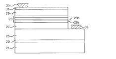
図1は、本発明の一実施例に係る発光素子を説明するための断面図である。図1を参照すると、前記発光素子は、n型窒化物半導体層25、活性層27、超格子構造のAlN/GaN層28、p型窒化物半導体層29を含む。また、前記発光素子は、基板21、バッファ層23、透明電極層31、n-電極33及びp-電極35を含むことができる。
FIG. 1 is a cross-sectional view illustrating a light emitting device according to an embodiment of the present invention. Referring to FIG. 1, the light emitting device includes an n-type
前記基板21は、窒化物系発光素子を製作するためのウェハーをいうもので、主にサファイア(Al2O3)またはシリコンカーバイド(SiC)であるが、これに限定されるものでなく、窒化物半導体層を成長させるのに適した異種基板、例えば、シリコン(Si)、ガリウム砒素(GaAs)、スピネルなどの異種基板、またはGaNなどの同種基板でもある。
The
バッファ層23は、基板21上に窒化物半導体層を成長させるとき、基板21と窒化物半導体層との間の格子不整合を緩和するためのもので、InAlGaN系列や、SiCまたはZnO系列の材料で形成される。
The
一方、n型窒化物半導体層25は、主にGaNで形成されるが、これに限定されるものでなく、(Al、In、Ga)N系列の2元系乃至4元系窒化物半導体で形成されることもある。また、n型窒化物半導体層25は、単一層または多重層で形成され、超格子層を含むことができる。
On the other hand, the n-type
活性層27は、単一量子井戸構造または多重量子井戸構造で形成され、多重量子井戸構
造の場合、量子障壁層と量子井戸層が交互に2回以上20回以下に反復形成される。前記活性層27は、要求される発光波長によって組成が決定され、青色及び緑色系列の可視光線を放出するためにはInGaNが活性層(量子井戸層)に適している。量子障壁層は、
前記量子井戸層に比べてバンドギャップの大きい窒化物、例えば、GaNまたはInGa
Nで形成される。
The
Nitride having a larger band gap than the quantum well layer, for example, GaN or InGa
N.
超格子構造のAlN/GaN層28は、活性層27とp型窒化物半導体層29との間にAlN28aとGaN28bが交互に反復的に成長されて形成された超格子構造を有する。超格子構造のAlN/GaN層28は、その上に成長されるp型窒化物半導体層29に電位が成長されることを遮断することができ、p型窒化物半導体層29の結晶性を高め、ホール濃度を高めることができ、AlN/GaN層28内へのMgの拡散も妨害し、所望の部分に適切にドーピングすることができる。このとき、AlN/GaN層28において、AlN及びGaNのうち少なくとも一つは、p型ドーパントがドーピングされたp型でなければならない。例えば、Mgがドーピングされたp型のAlNとu-GaN、Mgが
ドーピングされていないAlNとMgがドーピングされたp-GaN、Mgがドーピング
されたp型のAlNとMgがドーピングされたp-GaNである。ここでは、p型ドーパ
ントとしてMgを使用する場合を説明したが、本発明がこれに制限されることなく、その他にZnを使用することもできる。
The AlN / GaN layer 28 having a superlattice structure has a superlattice structure formed by alternately and repeatedly growing
併せて、前記超格子構造のAlN/GaN層28においては、GaN28bがAlN28aより厚く形成されることが好ましい。このようにすることで、Vfが高くなり、結晶質が低下する現象を防止することができる。
In addition, in the AlN / GaN layer 28 having the superlattice structure, the GaN 28b is preferably formed thicker than the
p型窒化物半導体層29は、主にGaNで形成されるが、これに限定されるものでなく、(AI、In、Ga)N系列の2元系乃至4元系窒化物半導体で形成される。また、p型窒化物半導体層29は、Mgをドーパントとして使用して形成される。
The p-type
前記p型窒化物半導体層29上に透明電極層31が位置し、透明電極層31は、Ni/Auなどの透明金属層またはITOなどの伝導性酸化物で形成される。
A
一方、n型窒化物半導体層25にn-電極33が形成され、透明電極層31上にp-電極が形成される。n-電極及びp-電極は、Ti/Alなどの多様な金属材料で形成される。
On the other hand, an n −
前記バッファ層、n型窒化物半導体層及び活性層は、金属有機化学気相成長法(Metal Organic Chemical Vapor Deposition;MOCVD)、分子線成長法(Molecular Beam Epitaxy;MBE)、水素化物気相成長法(Hydride Vapor Phase Epitaxy;HVPE)などの多様な技術を使用して形成されるが、現在には金属有機化学気相成長法が主に使用されている。したがって、以下では、金属有機化学気相成長法を使用して前記p型窒化物半導体層を形成する方法を説明する。 The buffer layer, the n-type nitride semiconductor layer, and the active layer may be formed by metal organic chemical vapor deposition (MOCVD), molecular beam epitaxy (MBE), hydride vapor deposition. Although formed using various techniques such as (Hydride Vapor Phase Epitaxy; HVPE), metal organic chemical vapor deposition is mainly used at present. Therefore, hereinafter, a method of forming the p-type nitride semiconductor layer using metal organic chemical vapor deposition will be described.
図2は、本発明の一実施例に係る発光素子を製造する方法を説明するためのフローチャートで、図3は、本発明の一実施例に係る発光素子を製造する方法を説明するためのタイミングダイアグラムである。 FIG. 2 is a flowchart for explaining a method of manufacturing a light emitting device according to an embodiment of the present invention, and FIG. 3 is a timing for explaining a method of manufacturing a light emitting device according to an embodiment of the present invention. It is a diagram.
図2を参照すると、まず、基板21が準備される(S0l)。前記基板21は、その上にバッファ層23、n型窒化物半導体層25及び活性層27を有する。このような基板21は、反応器内に基板21をローディングし、前記反応器内に各ソースガスを供給してバッファ層23、n型窒化物半導体層25及び活性層27を蒸着させることで準備される。
Referring to FIG. 2, first, a
前記バッファ層23は、窒化物で形成され、バッファ層の形成方法及び材料は既によく知られているので、それに対する詳細な説明は省略する。
The
前記n型窒化物半導体層25は、一般的にSiをドーパントとして使用して形成され、前記SiのソースとしてSiH4やSi2H4などの不活性ガスまたはDTBSiなどの金属有機物ソースを使用することができる。前記Si濃度は、1×10¹⁷/cm3〜5×1019/cm3の範囲であり、n型窒化物半導体層は、1.0〜5.0μmの厚さで形成される。
The n-type
前記活性層27は、単一量子井戸構造、またはInxGa11−xN(0.1<x<1)量子井戸層とInyGa1−yN(0<y<0.5)量子障壁層が2回以上20回以下に反復積層された多重量子井戸構造で形成される。各量子井戸層は、1〜5nmの厚さ及びIn含量(0.1<x<0.4)で形成され、各量子障壁層は、5〜40nmの厚さ及びIn含量(0<y<0.2)で形成されることが好ましい。
The
図2及び図3を参照すると、反応器内にp型ドーパントソース、Nソースガス、Alソースガスを供給してp型AlN層28aを成長させる(S03)。各ソースガスの供給は
、T1時間の間に行われる。
Referring to FIGS. 2 and 3, a p-
p型ドーパントソースとしては、CP2MgまたはDMZnを使用することができ、Nソースガスとしては、アンモニア(NH3)またはジメチルヒドラジン(DMHy)を使用することができ、Alソースガスとしては、トリメチルアルミニウム(trimethyl aluminum;TMAl、Al(CH3)3)を使用することができる。ここでは、p型ドーパントソースガスとしてMgソースガスであるCP2Mgを使用する場合を説明するが、本発明がこれに限定されることはない。 CP 2 Mg or DMZn can be used as the p-type dopant source, ammonia (NH 3 ) or dimethylhydrazine (DMHy) can be used as the N source gas, and trimethyl as the Al source gas. Aluminum (trimethyl aluminum; TMAl, Al (CH 3 ) 3 ) can be used. Here, a case where CP 2 Mg, which is an Mg source gas, is used as the p-type dopant source gas will be described, but the present invention is not limited to this.
前記T1時間は、要求される厚さのAlN層28aを形成するのに必要な時間に設定される。
The T1 time is set to a time necessary for forming the
その後、前記反応器内に供給されるMgソースガス及びAlソースガスの供給を中断し、p型AlN層の成長を中断させる(S05)。前記成長中断は、T2時間の間に行われる。 Thereafter, the supply of Mg source gas and Al source gas supplied to the reactor is interrupted, and the growth of the p-type AlN layer is interrupted (S05). The growth interruption is performed during T2.
反応器に排気ポンプが装着され、これによって反応器内のガスを排出させることで、前記各ソースガスの供給が中断された後、所定時間の経過とともに前記反応器内に残留するMgソースガス及びAlソースガスがほとんど外部に排出される。前記T2時間は、前記Mgソースガス及びAlソースガスを排出するための時間で、1乃至60秒である。 An exhaust pump is attached to the reactor, thereby exhausting the gas in the reactor, and after the supply of each source gas is interrupted, the Mg source gas remaining in the reactor with the passage of a predetermined time and Al source gas is almost discharged outside. The T2 time is 1 to 60 seconds for discharging the Mg source gas and the Al source gas.
相対的に高温状態で成長を中断させると、基板上に成長された窒化物半導体層で各窒素原子が解離されることで、各窒素空孔を形成することができる。したがって、窒素物半導体層の成長中断の間にNH3ガスを供給し、各N原子を供給することができる。本実施例において、前記NソースガスがNH3を含む場合、Mgソースガス及びAlソースガスの供給を中断し、NH3を継続的に供給することができる。これと異なり、前記NソースバスがNH3を含まない場合、前記成長中断段階(S05)でNH3を別途に供給することができる。 When the growth is interrupted at a relatively high temperature, each nitrogen vacancy can be formed by dissociating each nitrogen atom in the nitride semiconductor layer grown on the substrate. Therefore, NH 3 gas can be supplied during the interruption of the growth of the nitride semiconductor layer to supply each N atom. In this embodiment, when the N source gas contains NH 3 , the supply of the Mg source gas and the Al source gas can be interrupted, and NH 3 can be continuously supplied. Unlike this, the case of N source bus contains no NH 3, it is possible to supply NH 3 separately the growth interruption phase (S05).
その後、前記反応器内にGaソースガス及びNH3ガスを供給し、前記p型AlN層28a上にu-GaN層28bを成長させる(S07)。Gaソースとしては、トリメチル
ガリウム(TMGa)またはトリエチルガリウム(TEGa)を使用することができる。
Thereafter, Ga source gas and NH 3 gas are supplied into the reactor to grow a u-GaN layer 28b on the p-
前記u-GaN層28bの成長はT3時間の間行われ、T3は、1乃至60秒の範囲内
にある。
The growth of the u-GaN layer 28b is performed for T3 time, and T3 is in the range of 1 to 60 seconds.
その後、前記反応器内に供給されるGaソースガスの供給を中断し、u-GaN層28
bの成長を中断させる(S09)。前記成長中断は、T4時間の間行われる。
Thereafter, the supply of Ga source gas supplied into the reactor is interrupted, and the u-GaN layer 28
The growth of b is interrupted (S09). The growth interruption is performed for T4 time.
反応器に排気ポンプが装着され、これによって反応器内のガスを排出させることで、前記Gaソースガスの供給が中断された後、所定時間の経過とともに前記反応器内に残留するGaソースガスがほとんど外部に排出される。前記T4時間は、前記Gaソースガスを排出するための時間で、1乃至60秒である。 An exhaust pump is attached to the reactor, thereby discharging the gas in the reactor, so that the Ga source gas remaining in the reactor with the passage of a predetermined time after the supply of the Ga source gas is interrupted. Almost discharged outside. The T4 time is 1 to 60 seconds for discharging the Ga source gas.
以上説明したp型AlN層28aの成長、成長中断、u-GaN層28bの成長、成長
中断段階を複数回反復的に実施する(S11)。このとき、成長されるp型AlN層28a及びu-GaN層28bは、積層された全体厚さが300〜400Åで形成される。超
格子構造のAlN/GaN層28は、10乃至100対をなすことができる。これによって、超格子構造をなすp型AlN層28a及びu-GaN層28bのそれぞれの厚さは、
前記全体厚さを具現するための厚さに決定される。
The above-described growth, growth interruption of the p-
The thickness is determined to realize the total thickness.
MOCVDを使用して窒化物半導体層を成長させる場合、同一の反応器内でn型窒化物半導体層25、活性層27、超格子構造のAlN/GaN層28及びp型質貨物半導体層29が成長される。
When the nitride semiconductor layer is grown using MOCVD, the n-type
再び反応器内にGaソースガス、Nソースガス及びMgソースガスを供給し、Mgドーピングされたp型窒化物半導体層29を成長させる(S13)。 Again, Ga source gas, N source gas, and Mg source gas are supplied into the reactor to grow the Mg-doped p-type nitride semiconductor layer 29 (S13).
その後、前記基板21上に形成されたp型窒化物半導体層29及び活性層27をパターニングし、透明電極層31、n-電極33及びp-電極35を形成することで、図1の発光素子が完成される。
Thereafter, the p-type
本発明の各実施例によると、p型窒化物半導体層29と活性層27との間にp型AlN層28a及びu-GaN層28bが交互に積層された超格子構造のAlN/GaN層28
を形成することで、その上に成長される窒化物半導体層に電位が成長されることを遮断することができ、p型窒化物半導体層29の結晶性を高め、ホール濃度を高めることができ、AlN/GaN層28内へのMgの拡散も妨害し、所望の部分に適切にドーピングすることができる。
According to each embodiment of the present invention, an AlN / GaN layer 28 having a superlattice structure in which p-type AlN layers 28 a and u-GaN layers 28 b are alternately stacked between a p-type
By forming the layer, it is possible to block the potential from being grown on the nitride semiconductor layer grown thereon, increase the crystallinity of the p-type
<実験1> <Experiment 1>
実験1では、超格子構造のp型AlN/u-GaN層の成長時、Mgの流量変化による
光放出効果を測定した。
In Experiment 1, the light emission effect due to the change in the Mg flow rate was measured during the growth of the p-type AlN / u-GaN layer having a superlattice structure.
-温度:980℃ -Temperature: 980 ° C
-Mg 120sccm、180sccm、240sccm、300sccm、360sccm、480sccm -Mg 120sccm, 180sccm, 240sccm, 300sccm, 360sccm, 480sccm
-p型AlN/u-GaN層 60対、時間0.1分/0.1分 -p-type AlN / u-GaN layer 60 pairs, time 0.1 min / 0.1 min
図4は、Mgの流量変化による光放出量を示したグラフである。図4に示すように、超格子構造のAlN/GaN層を使用することで、全体的に光放出量が増加したことを確認することができる。AlN/GaN層の成長時、Mgの流量によって光放出量に差があっ
たし、Mgの流量が180sccm付近であるときに最上の光放出量が確認された。
FIG. 4 is a graph showing the light emission amount due to the change in the Mg flow rate. As shown in FIG. 4, it can be confirmed that the amount of light emission has increased as a whole by using the AlN / GaN layer having a superlattice structure. During the growth of the AlN / GaN layer, there was a difference in light emission amount depending on the Mg flow rate, and the highest light emission amount was confirmed when the Mg flow rate was around 180 sccm.
<実験2> <Experiment 2>
実験2では、超格子構造のp型AlN/u-GaN層の成長時、Alの流量変化による
光放出効果を測定した。
In Experiment 2, the light emission effect due to the change in the Al flow rate was measured during the growth of the p-type AlN / u-GaN layer having a superlattice structure.
-温度:980℃ -Temperature: 980 ° C
-Al;32/40/31(−10%);40/40/31;49/40/31(+1
0%)
-Al; 32/40/31 (-10%); 40/40/31; 49/40/31 (+1
0%)
-p型AlN/u-GaN層 60対、時間0.1分/0.1分 -p-type AlN / u-GaN layer 60 pairs, time 0.1 min / 0.1 min
図5は、Alの流量変化による光放出量を示したグラフである。図5に示すように、超格子構造のAlN/GaN層を使用することで、全体的に光放出量が増加したことを確認することができる。AlN/GaN層の成長時、Alの流量によって光放出量に差があったし、Alの流量が40sccm付近であるときに最上の光放出量が確認された。 FIG. 5 is a graph showing the light emission amount due to the change in the Al flow rate. As shown in FIG. 5, it can be confirmed that the amount of light emission has increased as a whole by using an AlN / GaN layer having a superlattice structure. During the growth of the AlN / GaN layer, there was a difference in the light emission amount depending on the Al flow rate, and the highest light emission amount was confirmed when the Al flow rate was around 40 sccm.
本実施例のp型窒化物半導体層形成方法は、発光ダイオードだけでなく、他の窒化物系光素子、例えば、レーザーダイオードを製造するために使用される。 The p-type nitride semiconductor layer forming method of the present embodiment is used for manufacturing not only a light-emitting diode but also other nitride-based optical elements such as a laser diode.
本発明を好ましい実施例を通して詳細に説明したが、本発明の範囲は、特定の実施例に限定されるものでなく、添付された特許請求の範囲によって解析されるべきである。また、この技術分野で通常の知識を習得した者であれば、本発明の範囲から逸脱することなく多くの修正と変形が可能であることを理解できるだろう。 Although the present invention has been described in detail through preferred embodiments, the scope of the present invention should not be limited to the specific embodiments, but should be analyzed by the appended claims. In addition, those skilled in the art will understand that many modifications and variations are possible without departing from the scope of the present invention.
例えば、本実施例では、超格子構造のAlN/GaN層を説明するとき、AlN層を先に成長させ、その後にGaN層を成長させる場合を説明したが、本発明は、これに制限されるものでなく、GaN層を先に成長させる工程を行い、その後にAlN層を成長させる工程を行うこともできる。 For example, in the present embodiment, when an AlN / GaN layer having a superlattice structure is described, the case where the AlN layer is grown first and then the GaN layer is grown is described. However, the present invention is limited to this. Instead, the step of growing the GaN layer first and the step of growing the AlN layer can be performed.
また、本実施例では、AlNとGaNを交互に積層して多数の対からなる超格子構造のAlN/GaN層を形成するとき、各対ごとにMgの量を一定にする場合を説明したが、本発明は、これに制限されるものでなく、AlN/GaN層の各対ごとにMgの量を漸次的に減少または増加させることで変化させることも可能である。 Further, in this embodiment, when AlN and GaN are alternately stacked to form an AlN / GaN layer having a superlattice structure composed of a large number of pairs, the amount of Mg is made constant for each pair. The present invention is not limited to this, but can be changed by gradually decreasing or increasing the amount of Mg for each pair of AlN / GaN layers.
また、本実施例では、p型AlNとu-GaNからなるAlN/GaNに対して説明し
たが、本発明は、これに制限されるものでない。
In this embodiment, AlN / GaN composed of p-type AlN and u-GaN has been described. However, the present invention is not limited to this.
例えば、前記超格子構造のAlN/GaN層の形成段階を行うとき、前記反応器内にMgソースガス、Nソースガス、Alソースガスを含む各ソースガスを供給し、前記活性層上にMgがドーピングされたp型AlN層を成長させ、前記反応器内に供給されるMgソースガス、Alソースガスの供給を中断して前記p型AlN層の成長を中断させ、NH3ガスを供給し、前記反応器内にMgソースガス、Gaソースガス及びNH3ガスを供給してp型AlN層上にp-GaN層を成長させ、前記反応器内に供給されるMgソースガス
、Gaソースガスの供給を中断してp-GaN層の成長を中断させ、NH3ガスを供給し
、前記過程を反復的に行うことで、Mgドーピングされたp型AlNとMgドーピングされたp-GaNからなる超格子構造のAlN/GaN層を形成することができる。
For example, when performing the step of forming the AlN / GaN layer having the superlattice structure, each source gas including Mg source gas, N source gas, and Al source gas is supplied into the reactor, and Mg is formed on the active layer. Growing a doped p-type AlN layer, interrupting the supply of Mg source gas and Al source gas supplied into the reactor to interrupt the growth of the p-type AlN layer, and supplying NH 3 gas; Mg source gas, Ga source gas and NH 3 gas are supplied into the reactor to grow a p-GaN layer on the p-type AlN layer, and Mg source gas and Ga source gas supplied into the reactor are grown. The supply is interrupted, the growth of the p-GaN layer is interrupted, NH 3 gas is supplied, and the above process is repeated, so that a superconducting layer composed of Mg-doped p-type AlN and Mg-doped p-GaN is formed. Lattice structure It can be formed of AlN / GaN layer.
また、前記超格子構造のAlN/GaN層の形成段階を行うとき、前記反応器内にNソースガス、Alソースガスを含む各ソースガスを供給して前記活性層上にAlN層を成長させ、前記反応器内に供給されるAlソースガスの供給を中断して前記AlN層の成長を中断させ、NH3ガスを供給し、前記反応器内にMgソースガス、Gaソースガス及びNH3ガスを供給してAlN層上にp-GaN層を成長させ、前記反応器内に供給されるM
gソースガス、Gaソースガスの供給を中断してp−GaN層の成長を中断させ、NH3ガスを供給し、前記過程を反復的に行うことで、MgドーピングされていないAlNとMgドーピングされたp-GaNからなる超格子構造のAlN/GaN層を形成することが
できる。
Further, when performing the formation step of the AlN / GaN layer having the superlattice structure, an NN gas is supplied into the reactor, and an AlN layer is grown on the active layer by supplying each source gas including an Al source gas, The supply of Al source gas supplied into the reactor is interrupted to stop the growth of the AlN layer, NH 3 gas is supplied, and Mg source gas, Ga source gas and NH 3 gas are supplied into the reactor. M is supplied to grow a p-GaN layer on the AlN layer and supplied into the reactor.
The supply of the g source gas and the Ga source gas is interrupted to stop the growth of the p-GaN layer, the NH 3 gas is supplied, and the above process is repeated, so that the MgN-doped AlN and the Mg-doped gas are doped. In addition, an AlN / GaN layer having a superlattice structure made of p-GaN can be formed.
併せて、本発明の一実施例では、p型ドーパントとしてMgを使用し、p型ドーパントソースガスとしてCp2Mgを使用した場合を説明したが、p型ドーパントとしてZnを使用し、p型ドーパントソースガスとしてDMZnを使用して具現することも可能である。 In addition, in the embodiment of the present invention, the case where Mg is used as the p-type dopant and Cp 2 Mg is used as the p-type dopant source gas has been described. However, Zn is used as the p-type dopant, and the p-type dopant is used. It is also possible to implement using DMZn as a source gas.
21 基板
23 バッファ層
25 n型窒化物半導体層
27 活性層
28 Aln/GaN層
29 p型窒化物半導体層
31 透明電極層
33 n-電極
35 p-電極
21
Claims (13)
前記n型窒化物半導体層上に形成された活性層と、
前記活性層上にAlNとGaNが交互に反復的に成長されて形成された超格子構造のAlN/GaN層と、
前記超格子構造のAlN/GaN層上に形成されたp型窒化物半導体層と、を含み、
前記超格子構造のAlNは、p型ドーパントがドーピングされたp型であり、前記GaNはu−GaNであることを特徴とする発光素子。 an n-type nitride semiconductor layer;
An active layer formed on the n-type nitride semiconductor layer;
An AlN / GaN layer having a superlattice structure formed by alternately and repeatedly growing AlN and GaN on the active layer;
A p-type nitride semiconductor layer formed on the AlN / GaN layer having the superlattice structure,
The Al N super lattice structure, p-type Der p-type dopant is doped is, the GaN light emitting device characterized u-GaN der Rukoto.
前記交互に反復的に成長された前記AlNと前記GaNからなる各対ごとにドーピングされるp型ドーパントの量が可変的であることを特徴とする請求項1に記載の発光素子。 The superlattice AlN / GaN layer is
The light emitting device according to claim 1, wherein the amount of p-type dopant doped for each pair of the AlN and the GaN grown alternately and repeatedly is variable.
前記n型窒化物半導体層上に活性層を形成する段階と、
前記活性層上にAlNとGaNを交互に反復的に成長させて超格子構造のAlN/GaN層を形成する段階と、
前記超格子構造のAlN/GaN層上にp型窒化物半導体層を形成する段階と、を含み、
前記超格子構造のAlNは、p型ドーパントがドーピングされたp型であり、前記GaNはu−GaNであることを特徴とする発光素子の製造方法。 Forming an n-type nitride semiconductor layer on the substrate;
Forming an active layer on the n-type nitride semiconductor layer;
AlN and GaN are alternately and repeatedly grown on the active layer to form a superlattice AlN / GaN layer;
Forming a p-type nitride semiconductor layer on the AlN / GaN layer having the superlattice structure,
The Al N super lattice structure, p-type Der p-type dopant is doped is, the GaN manufacturing method of the light emitting device characterized u-GaN der Rukoto.
反応器内で行われ、
前記反応器内にp型ドーパントソースガス、Nソースガス、Alソースガスを含む各ソースガスを供給し、前記活性層上にp型ドーパントがドーピングされたp型AlN層を成長させ、
前記反応器内に供給されるp型ドーパントソースガス、Alソースガスの 中断して前記p型AlN層の成長を中断させ、NH3ガスを供給し、
前記反応器内にGaソースガス及びNH3ガスを供給し、p型AlN層上にu-GaN層を成長させ、
前記反応器内に供給されるGaソースガスの供給を中断してu-GaN層の成長を中断させ、NH3ガスを供給し、
前記過程を反復的に行うことを特徴とする請求項6に記載の発光素子の製造方法。 The step of forming the superlattice AlN / GaN layer includes:
Performed in the reactor,
Each source gas including a p-type dopant source gas, an N source gas, and an Al source gas is supplied into the reactor, and a p-type AlN layer doped with a p-type dopant is grown on the active layer.
Interruption of the p-type dopant source gas and Al source gas supplied into the reactor to interrupt the growth of the p-type AlN layer, and supply NH 3 gas;
Ga source gas and NH 3 gas are supplied into the reactor, and a u-GaN layer is grown on the p-type AlN layer,
Interrupting the supply of the Ga source gas supplied into the reactor to interrupt the growth of the u-GaN layer, supplying NH 3 gas,
The method according to claim 6 , wherein the process is repeated.
前記反応器内にGaソースガス、Nソースガス、p型ドーパントソースガスを含む各ソースガスを供給し、前記基板上にp型ドーパントがドーピングされた前記p型窒化物半導体層を成長させることを含む請求項9に記載の発光素子の製造方法。 After performing the step of forming the superlattice AlN / GaN layer,
Each source gas including a Ga source gas, an N source gas, and a p-type dopant source gas is supplied into the reactor, and the p-type nitride semiconductor layer doped with the p-type dopant is grown on the substrate. The manufacturing method of the light emitting element of Claim 9 containing.
Applications Claiming Priority (2)
| Application Number | Priority Date | Filing Date | Title |
|---|---|---|---|
| KR10-2008-0027494 | 2008-03-25 | ||
| KR1020080027494A KR101308130B1 (en) | 2008-03-25 | 2008-03-25 | Light emitting device and method for fabricating the same |
Publications (2)
| Publication Number | Publication Date |
|---|---|
| JP2009239243A JP2009239243A (en) | 2009-10-15 |
| JP5322523B2 true JP5322523B2 (en) | 2013-10-23 |
Family
ID=40790902
Family Applications (1)
| Application Number | Title | Priority Date | Filing Date |
|---|---|---|---|
| JP2008183787A Expired - Fee Related JP5322523B2 (en) | 2008-03-25 | 2008-07-15 | Light emitting device and manufacturing method thereof |
Country Status (4)
| Country | Link |
|---|---|
| US (3) | US20090242870A1 (en) |
| EP (1) | EP2105974B1 (en) |
| JP (1) | JP5322523B2 (en) |
| KR (1) | KR101308130B1 (en) |
Families Citing this family (12)
| Publication number | Priority date | Publication date | Assignee | Title |
|---|---|---|---|---|
| US7902545B2 (en) * | 2008-05-14 | 2011-03-08 | Baker Hughes Incorporated | Semiconductor for use in harsh environments |
| WO2012058386A1 (en) * | 2010-10-27 | 2012-05-03 | The Regents Of The University Of California | METHOD FOR REDUCTION OF EFFICIENCY DROOP USING AN (A1,In,Ga)N/A1(x)In(1-x)N SUPERLATTICE ELECTRON BLOCKING LAYER IN NITRIDE BASED LIGHT EMITTING DIODES |
| KR20130129683A (en) * | 2012-05-21 | 2013-11-29 | 포항공과대학교 산학협력단 | Semiconductor light emitting device having graded superlattice electron blocking layer |
| KR101952437B1 (en) * | 2012-07-13 | 2019-04-25 | 엘지이노텍 주식회사 | Light emitting device, and method for fabricating the same |
| JP5874592B2 (en) * | 2012-09-21 | 2016-03-02 | 豊田合成株式会社 | Group III nitride semiconductor light emitting device manufacturing method |
| US20150243845A1 (en) * | 2014-02-26 | 2015-08-27 | Epistar Corporation | Light-emitting device |
| US9773889B2 (en) | 2014-07-18 | 2017-09-26 | Taiwan Semiconductor Manufacturing Company Limited | Method of semiconductor arrangement formation |
| CN106299051A (en) * | 2016-08-05 | 2017-01-04 | 华灿光电(浙江)有限公司 | A kind of LED epitaxial slice and preparation method thereof |
| US10516076B2 (en) | 2018-02-01 | 2019-12-24 | Silanna UV Technologies Pte Ltd | Dislocation filter for semiconductor devices |
| CN109166910B (en) * | 2018-09-06 | 2020-07-14 | 中山大学 | P-type AlGaN semiconductor material and epitaxial preparation method thereof |
| CN113471060B (en) * | 2021-05-27 | 2022-09-09 | 南昌大学 | Preparation method for reducing AlN film micro-holes on silicon substrate |
| CN115986014B (en) * | 2022-11-17 | 2024-04-12 | 淮安澳洋顺昌光电技术有限公司 | Epitaxial wafer provided with connecting layer and light-emitting diode comprising epitaxial wafer |
Family Cites Families (20)
| Publication number | Priority date | Publication date | Assignee | Title |
|---|---|---|---|---|
| US5270247A (en) * | 1991-07-12 | 1993-12-14 | Fujitsu Limited | Atomic layer epitaxy of compound semiconductor |
| JP2795294B2 (en) * | 1991-10-12 | 1998-09-10 | 日亜化学工業株式会社 | A method for growing a gallium aluminum nitride semiconductor crystal. |
| JPH09213641A (en) * | 1996-02-06 | 1997-08-15 | Oki Electric Ind Co Ltd | Method for forming hetero interface by organic metal vapor phase growth |
| US6677619B1 (en) * | 1997-01-09 | 2004-01-13 | Nichia Chemical Industries, Ltd. | Nitride semiconductor device |
| US6266355B1 (en) * | 1997-09-12 | 2001-07-24 | Sdl, Inc. | Group III-V nitride laser devices with cladding layers to suppress defects such as cracking |
| US6599133B2 (en) * | 1997-11-18 | 2003-07-29 | Technologies And Devices International, Inc. | Method for growing III-V compound semiconductor structures with an integral non-continuous quantum dot layer utilizing HVPE techniques |
| JP3497790B2 (en) * | 1999-11-29 | 2004-02-16 | 星和電機株式会社 | Method for manufacturing p-type gallium nitride based semiconductor and light emitting device using p-type gallium nitride based semiconductor |
| JP2001223429A (en) * | 2000-02-09 | 2001-08-17 | Fuji Photo Film Co Ltd | Semiconductor laser device |
| JP3453558B2 (en) * | 2000-12-25 | 2003-10-06 | 松下電器産業株式会社 | Nitride semiconductor device |
| JP4389723B2 (en) * | 2004-02-17 | 2009-12-24 | 住友電気工業株式会社 | Method for forming a semiconductor device |
| US7332365B2 (en) * | 2004-05-18 | 2008-02-19 | Cree, Inc. | Method for fabricating group-III nitride devices and devices fabricated using method |
| TWI266436B (en) * | 2004-07-30 | 2006-11-11 | Fujikura Ltd | Light-emitting device and method for manufacturing the same |
| JP2006128527A (en) * | 2004-11-01 | 2006-05-18 | Osaka Gas Co Ltd | Method of manufacturing garium nitride system compound semiconductor |
| US7910937B2 (en) * | 2005-02-02 | 2011-03-22 | Agency For Science, Technology And Research | Method and structure for fabricating III-V nitride layers on silicon substrates |
| JP2006245066A (en) * | 2005-02-28 | 2006-09-14 | Seiwa Electric Mfg Co Ltd | Light emitting diode and method of manufacturing light emitting diode |
| US7342261B2 (en) * | 2005-05-16 | 2008-03-11 | Dong-Sing Wuu | Light emitting device |
| JP5025168B2 (en) * | 2006-06-08 | 2012-09-12 | 昭和電工株式会社 | Method for producing group III nitride semiconductor multilayer structure |
| US7691757B2 (en) * | 2006-06-22 | 2010-04-06 | Asm International N.V. | Deposition of complex nitride films |
| EP1883140B1 (en) * | 2006-07-27 | 2013-02-27 | OSRAM Opto Semiconductors GmbH | LD or LED with superlattice clad layer and graded doping |
| US7723719B2 (en) * | 2007-12-14 | 2010-05-25 | Palo Alto Research Center Incorporated | Light emitting devices with inhomogeneous quantum well active regions |
-
2008
- 2008-03-25 KR KR1020080027494A patent/KR101308130B1/en active IP Right Grant
- 2008-07-14 EP EP08012675.8A patent/EP2105974B1/en not_active Not-in-force
- 2008-07-15 JP JP2008183787A patent/JP5322523B2/en not_active Expired - Fee Related
- 2008-08-18 US US12/193,588 patent/US20090242870A1/en not_active Abandoned
-
2009
- 2009-08-04 US US12/535,244 patent/US8716046B2/en active Active
-
2010
- 2010-05-06 US US12/775,119 patent/US8716048B2/en active Active
Also Published As
| Publication number | Publication date |
|---|---|
| US20090242870A1 (en) | 2009-10-01 |
| KR20090102203A (en) | 2009-09-30 |
| US8716046B2 (en) | 2014-05-06 |
| KR101308130B1 (en) | 2013-09-12 |
| US20090291519A1 (en) | 2009-11-26 |
| US8716048B2 (en) | 2014-05-06 |
| EP2105974A2 (en) | 2009-09-30 |
| US20100216272A1 (en) | 2010-08-26 |
| EP2105974B1 (en) | 2017-11-01 |
| EP2105974A3 (en) | 2012-08-22 |
| JP2009239243A (en) | 2009-10-15 |
Similar Documents
| Publication | Publication Date | Title |
|---|---|---|
| JP5322523B2 (en) | Light emitting device and manufacturing method thereof | |
| US8513694B2 (en) | Nitride semiconductor device and manufacturing method of the device | |
| US9911898B2 (en) | Ultraviolet light-emitting device | |
| JP5634368B2 (en) | Semiconductor device | |
| KR100784065B1 (en) | Nitride semiconductor led and fabrication method thereof | |
| US20060169990A1 (en) | Group III nitride-based compound semiconductor light-emitting device and method for producing the same | |
| JP6587673B2 (en) | Light emitting element | |
| US20210328099A1 (en) | Method of manufacturing nitride semiconductor light-emitting element | |
| KR20070081862A (en) | Nitride semiconductor light-emitting device and manufacturing method thereof | |
| KR20130102210A (en) | Nitride semiconductor light emitting device and manufacturing method thereof | |
| JP2007200933A (en) | Method of manufacturing nitride-based semiconductor element | |
| KR100925164B1 (en) | Method of forming p-type nitride semiconductor layer and light emitting device having the same | |
| KR100728132B1 (en) | Light-emitting diode using current spreading layer | |
| JP2009076864A (en) | Nitride-based light emitting device | |
| JP2007214378A (en) | Nitride-based semiconductor element | |
| KR100881053B1 (en) | Nitride based light emitting device | |
| JP2008227103A (en) | GaN-BASED SEMICONDUCTOR LIGHT EMITTING ELEMENT | |
| KR100906972B1 (en) | Nitride based light emitting device | |
| KR20120131147A (en) | Light emitting device and method for fabricating the same | |
| KR101423719B1 (en) | Light emitting device and method for fabricating the same | |
| KR100972974B1 (en) | Surface reformation method of Group ? nitride substrate, Group ? nitride substrate prepared therefrom, and nitride semiconductor light emitting device with the same | |
| JP2004158893A (en) | 3 group nitride semiconductor light emitting device | |
| JP2004274083A (en) | Group iii nitride semiconductor light-emitting element | |
| JP2004260219A (en) | 3 group nitride semiconductor luminous element | |
| KR100723177B1 (en) | FORMATION METHODS OF InGaN NITRIDE LAYER AND MULTI-QUANTUM WELL STRUCTURE ACTIVE LAYER |
Legal Events
| Date | Code | Title | Description |
|---|---|---|---|
| RD03 | Notification of appointment of power of attorney |
Free format text: JAPANESE INTERMEDIATE CODE: A7423 Effective date: 20091020 |
|
| RD04 | Notification of resignation of power of attorney |
Free format text: JAPANESE INTERMEDIATE CODE: A7424 Effective date: 20091021 |
|
| A621 | Written request for application examination |
Free format text: JAPANESE INTERMEDIATE CODE: A621 Effective date: 20110705 |
|
| A977 | Report on retrieval |
Free format text: JAPANESE INTERMEDIATE CODE: A971007 Effective date: 20120926 |
|
| A131 | Notification of reasons for refusal |
Free format text: JAPANESE INTERMEDIATE CODE: A131 Effective date: 20121002 |
|
| A601 | Written request for extension of time |
Free format text: JAPANESE INTERMEDIATE CODE: A601 Effective date: 20121226 |
|
| A602 | Written permission of extension of time |
Free format text: JAPANESE INTERMEDIATE CODE: A602 Effective date: 20130104 |
|
| A521 | Request for written amendment filed |
Free format text: JAPANESE INTERMEDIATE CODE: A523 Effective date: 20130125 |
|
| TRDD | Decision of grant or rejection written | ||
| A01 | Written decision to grant a patent or to grant a registration (utility model) |
Free format text: JAPANESE INTERMEDIATE CODE: A01 Effective date: 20130702 |
|
| A61 | First payment of annual fees (during grant procedure) |
Free format text: JAPANESE INTERMEDIATE CODE: A61 Effective date: 20130716 |
|
| R150 | Certificate of patent or registration of utility model |
Ref document number: 5322523 Country of ref document: JP Free format text: JAPANESE INTERMEDIATE CODE: R150 Free format text: JAPANESE INTERMEDIATE CODE: R150 |
|
| S531 | Written request for registration of change of domicile |
Free format text: JAPANESE INTERMEDIATE CODE: R313531 |
|
| S533 | Written request for registration of change of name |
Free format text: JAPANESE INTERMEDIATE CODE: R313533 |
|
| R350 | Written notification of registration of transfer |
Free format text: JAPANESE INTERMEDIATE CODE: R350 |
|
| R250 | Receipt of annual fees |
Free format text: JAPANESE INTERMEDIATE CODE: R250 |
|
| R250 | Receipt of annual fees |
Free format text: JAPANESE INTERMEDIATE CODE: R250 |
|
| R250 | Receipt of annual fees |
Free format text: JAPANESE INTERMEDIATE CODE: R250 |
|
| R250 | Receipt of annual fees |
Free format text: JAPANESE INTERMEDIATE CODE: R250 |
|
| R250 | Receipt of annual fees |
Free format text: JAPANESE INTERMEDIATE CODE: R250 |
|
| R250 | Receipt of annual fees |
Free format text: JAPANESE INTERMEDIATE CODE: R250 |
|
| LAPS | Cancellation because of no payment of annual fees |