JP5321832B2 - Liquid ejecting head, liquid ejecting apparatus, and actuator device - Google Patents

Liquid ejecting head, liquid ejecting apparatus, and actuator device Download PDF

Info

Publication number
JP5321832B2
JP5321832B2 JP2009183904A JP2009183904A JP5321832B2 JP 5321832 B2 JP5321832 B2 JP 5321832B2 JP 2009183904 A JP2009183904 A JP 2009183904A JP 2009183904 A JP2009183904 A JP 2009183904A JP 5321832 B2 JP5321832 B2 JP 5321832B2
Authority
JP
Japan
Prior art keywords
electrode
piezoelectric element
liquid ejecting
width direction
piezoelectric
Prior art date
Legal status (The legal status is an assumption and is not a legal conclusion. Google has not performed a legal analysis and makes no representation as to the accuracy of the status listed.)
Expired - Fee Related
Application number
JP2009183904A
Other languages
Japanese (ja)
Other versions
JP2010247511A (en
JP2010247511A5 (en
Inventor
宏行 亀井
Current Assignee (The listed assignees may be inaccurate. Google has not performed a legal analysis and makes no representation or warranty as to the accuracy of the list.)
Seiko Epson Corp
Original Assignee
Seiko Epson Corp
Priority date (The priority date is an assumption and is not a legal conclusion. Google has not performed a legal analysis and makes no representation as to the accuracy of the date listed.)
Filing date
Publication date
Application filed by Seiko Epson Corp filed Critical Seiko Epson Corp
Priority to JP2009183904A priority Critical patent/JP5321832B2/en
Publication of JP2010247511A publication Critical patent/JP2010247511A/en
Publication of JP2010247511A5 publication Critical patent/JP2010247511A5/ja
Application granted granted Critical
Publication of JP5321832B2 publication Critical patent/JP5321832B2/en
Expired - Fee Related legal-status Critical Current
Anticipated expiration legal-status Critical

Links

Images

Abstract

<P>PROBLEM TO BE SOLVED: To provide a liquid jetting head having improved drive durability, liquid jetting device, and actuator device. <P>SOLUTION: Reinforcing portions 65 composed of a material harder than the film forming a first electrode 60 are provided in the regions on the first electrode 60, wherein the regions correspond to both-end portions of a piezoelectric layer 70 in the width-direction of a piezoelectric element 300. The thickness of the reinforcing portions 65 is gradually reduced toward the inside of the width direction of the piezoelectric element 300. <P>COPYRIGHT: (C)2011,JPO&amp;INPIT

Description

本発明は、基板上に変位可能に設けられた圧電素子を有する液体噴射ヘッド及び液体噴射装置、並びにアクチュエーター装置に関する。   The present invention relates to a liquid ejecting head, a liquid ejecting apparatus, and an actuator device having a piezoelectric element displaceably provided on a substrate.

液体噴射ヘッド等に用いられる圧電素子は、電気機械変換機能を呈する圧電材料からなる圧電体層を2つの電極で挟んだ構成となっている。なお、液体噴射ヘッドの代表例としては、例えば、インク滴を吐出するノズル開口と連通する圧力発生室の一部を振動板で構成し、この振動板を圧電素子により変形させて圧力発生室のインクを加圧してノズル開口からインク滴を吐出させるインクジェット式記録ヘッド等がある。また、インクジェット式記録ヘッドに搭載される圧電素子としては、例えば、振動板の表面全体に亘って成膜技術により均一な圧電材料層を形成し、この圧電材料層をリソグラフィー法により圧力発生室に対応する形状に切り分けて圧力発生室毎に独立するように圧電素子を形成したものがある(例えば、特許文献1参照)。   A piezoelectric element used for a liquid ejecting head or the like has a configuration in which a piezoelectric layer made of a piezoelectric material exhibiting an electromechanical conversion function is sandwiched between two electrodes. As a typical example of the liquid ejecting head, for example, a part of the pressure generating chamber communicating with the nozzle opening for ejecting ink droplets is configured by a diaphragm, and the diaphragm is deformed by a piezoelectric element to There are ink jet recording heads that pressurize ink and eject ink droplets from nozzle openings. In addition, as a piezoelectric element mounted on the ink jet recording head, for example, a uniform piezoelectric material layer is formed over the entire surface of the diaphragm by a film forming technique, and this piezoelectric material layer is formed into a pressure generating chamber by a lithography method. There is one in which a piezoelectric element is formed so as to be separated into a corresponding shape and independent for each pressure generation chamber (for example, see Patent Document 1).

特開2003−163387号公報JP 2003-163387 A

しかしながら、駆動時には、振動板の圧電素子の幅方向両端部付近に応力が集中し、振動板が破壊されて、駆動耐久性が低下してしまうということがあった。   However, at the time of driving, stress concentrates in the vicinity of both ends in the width direction of the piezoelectric element of the diaphragm, and the diaphragm is broken, resulting in a decrease in driving durability.

なお、このような問題は、インクジェット式記録ヘッドに代表される液体噴射ヘッドに限定されず、他の装置に搭載されるアクチュエーター装置においても同様に存在する。   Such a problem is not limited to a liquid jet head typified by an ink jet recording head, and similarly exists in an actuator device mounted in another device.

本発明はこのような事情に鑑み、駆動耐久性を向上した液体噴射ヘッド及び液体噴射装置、並びにアクチュエーター装置を提供することを目的とする。   In view of such circumstances, it is an object of the present invention to provide a liquid ejecting head, a liquid ejecting apparatus, and an actuator device that have improved driving durability.

上記課題を解決する本発明の態様は、液体を噴射するノズル開口に連通する圧力発生室が並設された流路形成基板と、前記流路形成基板上に設けられた第1電極前記第1電極上に設けられた圧電体層及び前記圧電体層上に設けられた第2電極具備し、各圧力発生室に対応する圧電素子と、を備え、前記圧電素子は、前記圧力発生室の並設方向に沿った幅を持ち、前記第1電極上であって、前記圧電素子の幅方向における前記圧電体層の両端部に対応する領域、前記第1電極を形成する膜よりも硬い材料からなる補強部を有し、前記補強部は、前記圧電素子の幅方向内側に向かって厚さが漸小することを特徴とする液体噴射ヘッドにある。
かかる態様では、圧電体層の両端部に対応する領域に第1電極を形成する膜よりも硬い材料からなる補強部を設けることにより、圧電素子の幅方向端部における応力集中に対する第1電極の剛性が高まり、圧電素子の駆動耐久性を向上させることができる。また、補強部は、圧電素子の幅方向内側に向かって厚さが漸小することにより、圧電素子の幅方向端部における応力を分散させて、応力集中を抑制することができる。

Aspect of the present invention for solving the above-mentioned problems, and the flow path forming substrate pressure generating chambers are arranged communicating with nozzle openings for ejecting a liquid, a first electrode provided on the passage forming substrate, said first comprising a second electrode provided on the first piezoelectric layer provided on the electrode and the piezoelectric layer, and a piezoelectric element corresponding to each pressure generating chamber, the piezoelectric element, the pressure generating chamber has a width along the arrangement direction, the first a on the electrode, the at the region corresponding to both ends of the piezoelectric layer in the width direction of the piezoelectric element, than the membrane that forms the first electrode The liquid ejecting head includes a reinforcing portion made of a hard material , and the thickness of the reinforcing portion gradually decreases toward the inner side in the width direction of the piezoelectric element.
In such an aspect, by providing a reinforcing portion made of a material harder than the film forming the first electrode in a region corresponding to both ends of the piezoelectric layer, the first electrode has a resistance against stress concentration at the widthwise end portion of the piezoelectric element. The rigidity is increased, and the driving durability of the piezoelectric element can be improved. Further, the reinforcing portion is gradually reduced in thickness toward the inner side in the width direction of the piezoelectric element, whereby the stress at the end portion in the width direction of the piezoelectric element can be dispersed to suppress stress concentration.

前記補強部は、ビッカース硬度Hvが1000以上の材料からなるのが好ましい。これによれば、効果的に圧電素子の駆動耐久性を向上させることができる。   The reinforcing portion is preferably made of a material having a Vickers hardness Hv of 1000 or more. According to this, it is possible to effectively improve the driving durability of the piezoelectric element.

前記補強部から連続して前記圧電素子の幅方向外側に延設される腕部を具備するのが好ましい。これによれば、腕部がエッチングストップ層として機能し、第1電極の膜厚のばらつきを抑制することができる。これにより、圧電素子の共振周波数および変位量のばらつきを抑制したものとすることができる。   It is preferable that an arm portion extending continuously outward from the reinforcing portion in the width direction of the piezoelectric element is provided. According to this, an arm part functions as an etching stop layer, and can suppress the dispersion | variation in the film thickness of a 1st electrode. Thereby, the dispersion | variation in the resonant frequency and displacement amount of a piezoelectric element can be suppressed.

前記腕部は、前記補強部よりも厚さが薄いのが好ましい。これによれば、第1電極の高い変位量を確保しつつ、圧電素子の駆動耐久性を向上させることができる。   The arm portion is preferably thinner than the reinforcing portion. According to this, it is possible to improve the driving durability of the piezoelectric element while securing a high displacement amount of the first electrode.

前記補強部と前記腕部の境界部分には凹部が設けられており、且つ該凹部の内面が曲面状となっているのが好ましい。これによれば、圧電素子の幅方向端部における第1電極にかかる応力をより効果的に分散させることができる。   It is preferable that a concave portion is provided at a boundary portion between the reinforcing portion and the arm portion, and an inner surface of the concave portion is curved. According to this, the stress applied to the first electrode at the end in the width direction of the piezoelectric element can be more effectively dispersed.

前記第1電極上であって前記圧電素子の幅方向中央部には、前記第1電極を形成する膜よりも硬い材料からなる第2の補強部が前記圧力発生室の長手方向に亘って設けられているのが好ましい。これによれば、圧電素子の長手方向の駆動耐久性を向上させることができる。   A second reinforcing portion made of a material harder than the film forming the first electrode is provided in the longitudinal direction of the pressure generating chamber on the first electrode and in the center in the width direction of the piezoelectric element. It is preferred that According to this, the driving durability in the longitudinal direction of the piezoelectric element can be improved.

前記第2の補強部は、前記圧電素子の幅方向外側に向かって厚さが漸小するのが好ましい。これによれば、第2の補強部に対する応力を分散させて、応力集中を抑制することができる。   It is preferable that the thickness of the second reinforcing portion gradually decreases toward the outer side in the width direction of the piezoelectric element. According to this, the stress with respect to the 2nd reinforcement part can be disperse | distributed, and stress concentration can be suppressed.

少なくとも前記圧電体層の側面を覆う絶縁体からなる被覆膜が設けられているのが好ましい。これによれば、大気中の水分に起因する圧電素子の破壊を抑制することができる。   It is preferable that a coating film made of an insulator covering at least the side surface of the piezoelectric layer is provided. According to this, destruction of the piezoelectric element due to moisture in the atmosphere can be suppressed.

さらに本発明の他の態様は、上記態様の液体噴射ヘッドを具備することを特徴とする液体噴射装置にある。
かかる態様では、信頼性を向上した液体噴射装置を実現できる。
According to still another aspect of the invention, there is provided a liquid ejecting apparatus including the liquid ejecting head according to the above aspect.
In this aspect, a liquid ejecting apparatus with improved reliability can be realized.

さらに本発明の他の態様は、基板上に設けられた第1電極と、前記第1電極上に設けられた圧電体層と、前記圧電体層上に設けられた第2電極とを具備する圧電素子を備え、前記第1電極上であって、前記圧電素子の幅方向における前記圧電体層の両端部に対応する領域には、前記第1電極を形成する膜よりも硬い材料からなる補強部が設けられ、前記補強部は、前記圧電素子の幅方向内側に向かって厚さが漸小することを特徴とするアクチュエーター装置にある。
かかる態様では、圧電体層の両端部に対応する領域に第1電極を形成する膜よりも硬い材料からなる補強部を設けることにより、圧電素子の幅方向端部における応力集中に対する第1電極の剛性が高まり、圧電素子の駆動耐久性を向上させることができる。また、補強部は、圧電素子の幅方向内側に向かって厚さが漸小することにより、圧電素子の幅方向端部における応力を分散させて、応力集中を抑制することができる。
Furthermore, another aspect of the present invention includes a first electrode provided on a substrate, a piezoelectric layer provided on the first electrode, and a second electrode provided on the piezoelectric layer. Reinforcement made of a material harder than the film forming the first electrode in a region corresponding to both end portions of the piezoelectric layer in the width direction of the piezoelectric element on the first electrode. The actuator device is characterized in that a thickness is gradually reduced toward the inner side in the width direction of the piezoelectric element.
In such an aspect, by providing a reinforcing portion made of a material harder than the film forming the first electrode in a region corresponding to both ends of the piezoelectric layer, the first electrode has a resistance against stress concentration at the widthwise end portion of the piezoelectric element. The rigidity is increased, and the driving durability of the piezoelectric element can be improved. Further, the reinforcing portion is gradually reduced in thickness toward the inner side in the width direction of the piezoelectric element, whereby the stress at the end portion in the width direction of the piezoelectric element can be dispersed to suppress stress concentration.

実施形態1に係る記録ヘッドの概略構成を示す分解斜視図。FIG. 3 is an exploded perspective view illustrating a schematic configuration of the recording head according to the first embodiment. 実施形態1に係る記録ヘッドの平面図及び断面図。2A and 2B are a plan view and a cross-sectional view of the recording head according to the first embodiment. 実施形態1に係る記録ヘッドの要部断面図。FIG. 3 is a cross-sectional view of a main part of the recording head according to the first embodiment. 実施形態1に係る記録ヘッドの要部平面図。FIG. 3 is a plan view of a main part of the recording head according to the first embodiment. 実施形態1に係る記録ヘッドの製造方法を示す断面図。FIG. 3 is a cross-sectional view illustrating the method for manufacturing the recording head according to the first embodiment. 実施形態1に係る記録ヘッドの製造方法を示す断面図。FIG. 3 is a cross-sectional view illustrating the method for manufacturing the recording head according to the first embodiment. 実施形態1に係る記録ヘッドの製造方法を示す断面図。FIG. 3 is a cross-sectional view illustrating the method for manufacturing the recording head according to the first embodiment. 実施形態1に係る記録装置の概略構成を示す斜視図。FIG. 2 is a perspective view illustrating a schematic configuration of the recording apparatus according to the first embodiment. 実施形態2に係る記録ヘッドの圧電素子及び圧力発生室の要部断面図。FIG. 6 is a cross-sectional view of a main part of a piezoelectric element and a pressure generation chamber of a recording head according to a second embodiment. 実施形態3に係る記録ヘッドの圧電素子及び圧力発生室の要部断面図。FIG. 9 is a cross-sectional view of a main part of a piezoelectric element and a pressure generation chamber of a recording head according to a third embodiment. 実施形態4に係る記録ヘッドの圧電素子及び圧力発生室の要部断面図。FIG. 6 is a cross-sectional view of main parts of a piezoelectric element and a pressure generation chamber of a recording head according to a fourth embodiment.

以下に本発明を実施形態に基づいて詳細に説明する。
(実施形態1)
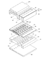
図1は、本発明の実施形態1に係る液体噴射ヘッドの一例であるインクジェット式記録ヘッドの概略構成を示す分解斜視図であり、図2は、流路形成基板の平面図及びそのA−A′断面図であり、図3は、図2(b)のB−B’断面図である。
Hereinafter, the present invention will be described in detail based on embodiments.
(Embodiment 1)
FIG. 1 is an exploded perspective view showing a schematic configuration of an ink jet recording head which is an example of a liquid jet head according to Embodiment 1 of the present invention. FIG. 2 is a plan view of a flow path forming substrate and its AA. 'Is a sectional view, and FIG. 3 is a sectional view taken along the line BB ′ of FIG.

図示するように、流路形成基板10は、本実施形態ではシリコン単結晶基板からなり、その一方の面には酸化膜からなる弾性膜50が形成されている。   As shown in the drawing, the flow path forming substrate 10 is made of a silicon single crystal substrate in the present embodiment, and an elastic film 50 made of an oxide film is formed on one surface thereof.

流路形成基板10には、複数の圧力発生室12がその幅方向に並設されている。また、流路形成基板10の圧力発生室12の長手方向外側の領域には連通部13が形成され、連通部13と各圧力発生室12とが、各圧力発生室12毎に設けられたインク供給路14及び連通路15を介して連通されている。連通部13は、後述する保護基板のリザーバー部31と連通して各圧力発生室12の共通のインク室となるリザーバーの一部を構成する。インク供給路14は、圧力発生室12よりも狭い幅で形成されており、連通部13から圧力発生室12に流入するインクの流路抵抗を一定に保持している。なお、本実施形態では、流路の幅を片側から絞ることでインク供給路14を形成したが、流路の幅を両側から絞ることでインク供給路を形成してもよい。また、流路の幅を絞るのではなく、厚さ方向から絞ることでインク供給路を形成してもよい。   A plurality of pressure generating chambers 12 are arranged in parallel in the width direction of the flow path forming substrate 10. In addition, a communication portion 13 is formed in a region outside the longitudinal direction of the pressure generation chamber 12 of the flow path forming substrate 10, and the communication portion 13 and each pressure generation chamber 12 are provided for each pressure generation chamber 12. Communication is made via a supply path 14 and a communication path 15. The communication part 13 communicates with a reservoir part 31 of a protective substrate, which will be described later, and constitutes a part of a reservoir that becomes a common ink chamber of each pressure generating chamber 12. The ink supply path 14 is formed with a narrower width than the pressure generation chamber 12, and maintains a constant flow path resistance of ink flowing into the pressure generation chamber 12 from the communication portion 13. In this embodiment, the ink supply path 14 is formed by narrowing the width of the flow path from one side. However, the ink supply path may be formed by narrowing the width of the flow path from both sides. Further, the ink supply path may be formed by narrowing from the thickness direction instead of narrowing the width of the flow path.

また、流路形成基板10の開口面側には、各圧力発生室12のインク供給路14とは反対側の端部近傍に連通するノズル開口21が穿設されたノズルプレート20が、接着剤や熱溶着フィルム等によって固着されている。なお、ノズルプレート20は、例えばガラスセラミックス、シリコン単結晶基板又はステンレス鋼などからなる。   Further, on the opening surface side of the flow path forming substrate 10, a nozzle plate 20 having a nozzle opening 21 communicating with the vicinity of the end of each pressure generating chamber 12 on the side opposite to the ink supply path 14 is provided with an adhesive. Or a heat-welded film or the like. The nozzle plate 20 is made of, for example, glass ceramics, a silicon single crystal substrate, or stainless steel.

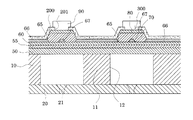
一方、このような流路形成基板10の開口面とは反対側には、上述したように、弾性膜50が形成され、この弾性膜50上には、絶縁体膜55が形成されている。さらに、この絶縁体膜55上には、第1電極60と圧電体層70と第2電極80とが、後述するプロセスで積層形成されて、圧電素子300を構成している。ここで、圧電素子300は、第1電極60、圧電体層70及び第2電極80を含む部分をいう。一般的には、圧電素子300の何れか一方の電極を共通電極とし、他方の電極及び圧電体層70を各圧力発生室12毎にパターニングして構成する。そして、ここではパターニングされた何れか一方の電極及び圧電体層70から構成され、両電極への電圧の印加により圧電歪みが生じる部分を圧電体能動部という。本実施形態では、第1電極60を圧電素子300の共通電極とし、第2電極80を圧電素子300の個別電極としているが、駆動回路や配線の都合でこれを逆にしても支障はない。   On the other hand, the elastic film 50 is formed on the side opposite to the opening surface of the flow path forming substrate 10 as described above, and the insulator film 55 is formed on the elastic film 50. Further, the first electrode 60, the piezoelectric layer 70, and the second electrode 80 are laminated on the insulator film 55 by a process described later to constitute the piezoelectric element 300. Here, the piezoelectric element 300 refers to a portion including the first electrode 60, the piezoelectric layer 70, and the second electrode 80. In general, one electrode of the piezoelectric element 300 is used as a common electrode, and the other electrode and the piezoelectric layer 70 are patterned for each pressure generating chamber 12. In addition, here, a portion that is configured by any one of the patterned electrodes and the piezoelectric layer 70 and in which piezoelectric distortion is generated by applying a voltage to both electrodes is referred to as a piezoelectric active portion. In the present embodiment, the first electrode 60 is a common electrode of the piezoelectric element 300, and the second electrode 80 is an individual electrode of the piezoelectric element 300. However, there is no problem even if this is reversed for the convenience of the drive circuit and wiring.

圧電体層70は、第1電極60上に形成される電気機械変換作用を示す圧電材料、特に圧電材料の中でもペロブスカイト構造の強誘電体材料からなる。圧電体層70は、ペロブスカイト構造の結晶膜を用いるのが好ましく、例えば、チタン酸ジルコン酸鉛(PZT)等の強誘電体材料や、これに酸化ニオブ、酸化ニッケル又は酸化マグネシウム等の金属酸化物を添加したもの等が好適である。   The piezoelectric layer 70 is made of a piezoelectric material that is formed on the first electrode 60 and has an electromechanical conversion effect, and in particular, a ferroelectric material having a perovskite structure among the piezoelectric materials. The piezoelectric layer 70 is preferably a crystal film having a perovskite structure. For example, a ferroelectric material such as lead zirconate titanate (PZT) or a metal oxide such as niobium oxide, nickel oxide, or magnesium oxide is used. Those to which is added are suitable.

図2及び3に示すように、本実施形態では、第1電極60の圧力発生室12の長手方向の端部(圧電素子300の長手方向の端部)を圧力発生室12に相対向する領域内に設けることで、圧電素子300の実質的な駆動部となる圧電体能動部の長手方向の端部(長さ)を規定している。また、第2電極80の圧力発生室12の短手方向の端部(圧電素子300の短手方向の端部)を圧力発生室12に相対向する領域内に設けることで、圧電体能動部の短手方向の端部(幅)を規定している。すなわち、圧電体能動部は、パターニングされた第1電極60及び第2電極80によって、圧力発生室12に相対向する領域にのみ設けられていることになる。さらに、本実施形態では、圧電体層70及び第2電極80が、図3に示すように、第2電極80側の幅が狭くなるようにパターニングされ、その側面は傾斜面となっている。   As shown in FIGS. 2 and 3, in the present embodiment, a region in which the end portion in the longitudinal direction of the pressure generation chamber 12 of the first electrode 60 (the end portion in the longitudinal direction of the piezoelectric element 300) is opposed to the pressure generation chamber 12. By providing the inside, the end portion (length) in the longitudinal direction of the piezoelectric active portion serving as a substantial driving portion of the piezoelectric element 300 is defined. Further, by providing an end in the short direction of the pressure generation chamber 12 of the second electrode 80 (an end in the short direction of the piezoelectric element 300) in a region facing the pressure generation chamber 12, the piezoelectric active portion The end portion (width) in the short direction is defined. That is, the piezoelectric active part is provided only in a region opposite to the pressure generating chamber 12 by the patterned first electrode 60 and second electrode 80. Furthermore, in this embodiment, as shown in FIG. 3, the piezoelectric layer 70 and the second electrode 80 are patterned so that the width on the second electrode 80 side is narrow, and the side surfaces thereof are inclined surfaces.

ここで、圧電素子300を所定の基板上に設け、当該圧電素子300を駆動させる装置をアクチュエーター装置と称する。本実施形態では、弾性膜50、絶縁体膜55及び第1電極60が振動板として作用するが、勿論これに限定されるものではなく、例えば、弾性膜50及び絶縁体膜55を設けずに、第1電極60のみが振動板として作用するようにしてもよい。   Here, a device for providing the piezoelectric element 300 on a predetermined substrate and driving the piezoelectric element 300 is referred to as an actuator device. In the present embodiment, the elastic film 50, the insulator film 55, and the first electrode 60 function as a diaphragm, but of course not limited to this, for example, without providing the elastic film 50 and the insulator film 55. Only the first electrode 60 may act as a diaphragm.

また、図3に示すように、第1電極60上であって、圧電素子300の幅方向における圧電体層70の両端部に対応する領域には、第1電極60を形成する膜よりも硬い材料からなる補強部65が設けられている。この補強部65は、第1電極60上であって圧電素子300の幅方向における圧電体層70の両端部に対応する領域、具体的には、第1電極60と圧電体層70との間に設けられている。そして、この補強部65から連続して圧電素子300の幅方向外側に腕部66が延設されている。このように補強部65と腕部66は一体であり、補強膜を構成している。   Further, as shown in FIG. 3, the region on the first electrode 60 and corresponding to both ends of the piezoelectric layer 70 in the width direction of the piezoelectric element 300 is harder than the film forming the first electrode 60. A reinforcing portion 65 made of a material is provided. The reinforcing portion 65 is a region on the first electrode 60 corresponding to both end portions of the piezoelectric layer 70 in the width direction of the piezoelectric element 300, specifically, between the first electrode 60 and the piezoelectric layer 70. Is provided. An arm portion 66 extends continuously from the reinforcing portion 65 to the outside in the width direction of the piezoelectric element 300. Thus, the reinforcement part 65 and the arm part 66 are integral, and comprise the reinforcement film | membrane.

言い換えれば、補強膜は、第1電極60と圧電体層70との間に設けられている補強部65と、補強部65から連続して圧電素子300の幅方向外側に延設する腕部66とからなり、圧電素子300に対向する領域に開口しており、端部が圧電体層70に入り込むように設けられている。   In other words, the reinforcing film includes a reinforcing portion 65 provided between the first electrode 60 and the piezoelectric layer 70, and an arm portion 66 extending continuously from the reinforcing portion 65 to the outside in the width direction of the piezoelectric element 300. And has an opening in a region facing the piezoelectric element 300, and an end portion is provided so as to enter the piezoelectric layer 70.

上述した補強部65は、圧電素子300の幅方向内側に向かって厚さが漸小している。すなわち、補強膜の端部は、圧力発生室12側に向かって厚さが漸小するテーパー状となっている。   The reinforcing portion 65 described above gradually decreases in thickness toward the inner side in the width direction of the piezoelectric element 300. That is, the end portion of the reinforcing film has a tapered shape whose thickness gradually decreases toward the pressure generating chamber 12 side.

なお、本実施形態では、腕部66は、圧力発生室12を並設方向に区画する隔壁11に対応する領域まで延設されている。   In the present embodiment, the arm portion 66 extends to a region corresponding to the partition wall 11 that partitions the pressure generation chamber 12 in the juxtaposition direction.

この補強部65は、少なくとも圧電体層70の両端部に対応する領域に設ければよく、圧電素子300(圧電体能動部)の変位を阻害しない範囲であれば、圧電体能動部に対向する領域まで設けられていてもよい。   The reinforcing portion 65 may be provided in a region corresponding to at least both ends of the piezoelectric layer 70, and is opposed to the piezoelectric active portion as long as the displacement of the piezoelectric element 300 (piezoelectric active portion) is not hindered. It may be provided up to the area.

ここで、図4は、流路形成基板上の補強部65、腕部66、及び後述する第2の補強部67の平面図である。   Here, FIG. 4 is a plan view of the reinforcing portion 65, the arm portion 66, and the second reinforcing portion 67 described later on the flow path forming substrate.

図3及び図4に示すように、第1電極60上であって圧電素子300の幅方向中央部には、第1電極60を形成する膜よりも硬い材料からなる第2の補強部67が圧力発生室12の長手方向に亘って設けられている。本実施形態では、第2の補強部67は、端部が圧力発生室12の長手方向端部よりも外側となるように設けた。また、第2の補強部67の両端部は、圧電素子300の幅方向外側に向かって厚さが漸小している。なお、本実施形態では、第2の補強部67は、端部が圧力発生室12の長手方向端部よりも外側となるように設けたが、第2の補強部67は、長手方向に亘って設けられていればよい。例えば、第2の補強部67は、端部が圧力発生室12の長手方向端部より外側であっても内側であってもよく、間欠的に設けられていてもよい。   As shown in FIGS. 3 and 4, a second reinforcing portion 67 made of a material harder than the film forming the first electrode 60 is provided on the first electrode 60 and in the center in the width direction of the piezoelectric element 300. It is provided over the longitudinal direction of the pressure generating chamber 12. In the present embodiment, the second reinforcing portion 67 is provided so that the end portion is outside the longitudinal end portion of the pressure generating chamber 12. In addition, both end portions of the second reinforcing portion 67 are gradually reduced in thickness toward the outer side in the width direction of the piezoelectric element 300. In the present embodiment, the second reinforcing portion 67 is provided so that the end portion is outside the longitudinal end portion of the pressure generating chamber 12, but the second reinforcing portion 67 extends in the longitudinal direction. As long as it is provided. For example, the end of the second reinforcing portion 67 may be outside or inside the longitudinal end of the pressure generating chamber 12 or may be provided intermittently.

ここで、補強膜(補強部65及び腕部66)及び第2の補強部67は、第1電極60を形成する膜よりも硬い材料からなる。補強部65、腕部66及び第2の補強部67の材料は、ビッカース硬度Hvが1000以上であるのが好ましく、例えば、ダイヤモンドライクカーボン(DLC)、炭窒化チタン(TiCN)、窒化チタンアルミ(TiAlN)、酸化アルミニウム(Al)、二ホウ化チタン(TiB)、炭化バナジウム(VC)、炭化チタン(TiC)、五ホウ化二タングステン(W)、二ホウ化ニオブ(NbB)、炭化ジルコニウム(ZrC)、六ホウ化ランタン(LaB)、炭化タングステン(WC)、五ホウ化二モリブデン(Mo)、二ホウ化ジルコニウム(ZrB)、二ホウ化クロム(CrB)、二炭化三クロム(Cr)、二ホウ化バナジウム(VB)、二ホウ化タンタル(TaB)、窒化チタン(TiN)、炭化ニオブ(NbC)、炭化二モリブデン(MoC)、窒化ジルコニウム(ZrN)、窒化バナジウム(VN)、炭化タンタル(TaC)、窒化ニオブ(NbN)、窒化クロム(CrN)が挙げられる。補強部65及び腕部66と、第2の補強部67の材料は、後述するように同時に成形することができるという点から同一のものからなるのが好ましいが、異なるものであってもよい。また、補強部65、腕部66、及び第2の補強部67の厚さは、特に限定されるものではなく、振動板の変位量を大きく低下させない程度であればよい。本実施形態では、厚さ50nmのダイヤモンドライクカーボン(DLC)を用いた。 Here, the reinforcing film (the reinforcing part 65 and the arm part 66) and the second reinforcing part 67 are made of a material harder than the film forming the first electrode 60. The material of the reinforcing portion 65, the arm portion 66, and the second reinforcing portion 67 preferably has a Vickers hardness Hv of 1000 or more. For example, diamond-like carbon (DLC), titanium carbonitride (TiCN), titanium nitride aluminum ( TiAlN), aluminum oxide (Al 2 O 3 ), titanium diboride (TiB 2 ), vanadium carbide (VC), titanium carbide (TiC), ditungsten pentaboride (W 2 B 5 ), niobium diboride ( NbB 2 ), zirconium carbide (ZrC), lanthanum hexaboride (LaB 6 ), tungsten carbide (WC), dimolybdenum pentaboride (Mo 2 B 5 ), zirconium diboride (ZrB 2 ), chromium diboride (CrB 2), two carbide three chromium (Cr 3 C 2), diboride, vanadium (VB 2), diboride, tantalum (TaB 2) Titanium nitride (TiN), niobium carbide (NbC), carbide Molybdenum (Mo 2 C), zirconium nitride (ZrN), vanadium nitride (VN), tantalum carbide (TaC), niobium nitride (NbN), chromium nitride (CrN) Is mentioned. The materials of the reinforcing portion 65 and the arm portion 66 and the second reinforcing portion 67 are preferably made of the same material from the viewpoint that they can be molded simultaneously as described later, but may be different. Moreover, the thickness of the reinforcement part 65, the arm part 66, and the 2nd reinforcement part 67 is not specifically limited, What is necessary is just a grade which does not reduce the displacement amount of a diaphragm significantly. In this embodiment, diamond-like carbon (DLC) having a thickness of 50 nm is used.

このように、圧電体層70の幅方向両端部に対応する領域に、第1電極60よりも硬い材料からなる補強部65を設けることにより、圧電素子300の幅方向端部における応力集中に対する第1電極60の剛性が高まり、圧電素子300の駆動耐久性を向上させることができる。言い換えれば、圧電素子300の駆動を繰り返しても第1電極60を含む振動板が破壊される虞がなくなる。   As described above, by providing the reinforcing portions 65 made of a material harder than the first electrode 60 in the regions corresponding to the both ends in the width direction of the piezoelectric layer 70, the stress concentration at the end portions in the width direction of the piezoelectric element 300 is reduced. The rigidity of one electrode 60 is increased, and the driving durability of the piezoelectric element 300 can be improved. In other words, there is no possibility that the diaphragm including the first electrode 60 is broken even if the driving of the piezoelectric element 300 is repeated.

また、補強部65は、圧電素子300の幅方向内側に向かって厚さが漸小していることにより、圧電素子300の幅方向端部における応力を分散させて、第1電極60への応力集中を抑制することができる。これにより、第1電極60を含む振動板の破壊が抑制されて、圧電素子300の駆動耐久性を向上させることができる。また、圧電体層70との接触面積が小さくても第1電極60との接触面積を確保することができるため、圧電素子300の変位特性を低下させることなく、圧電素子300の駆動耐久性を向上させることができる。   Further, since the reinforcing portion 65 gradually decreases in thickness toward the inner side in the width direction of the piezoelectric element 300, the stress at the end portion in the width direction of the piezoelectric element 300 is dispersed and the stress on the first electrode 60 is reduced. Concentration can be suppressed. Thereby, destruction of the diaphragm including the first electrode 60 is suppressed, and the driving durability of the piezoelectric element 300 can be improved. Further, since the contact area with the first electrode 60 can be ensured even if the contact area with the piezoelectric layer 70 is small, the driving durability of the piezoelectric element 300 can be improved without deteriorating the displacement characteristics of the piezoelectric element 300. Can be improved.

また、腕部66が圧力発生室12を並設方向に区画する隔壁に対応する領域まで延設されていることにより、圧電体層70や第2電極80をエッチングにより形成する際に、腕部66がエッチングストップ層として作用する。圧電体層70を腕部66が露出するまでエッチングすることにより実質的にエッチングが停止する。これにより、第1電極60がエッチングされることがなく、第1電極60の膜厚のばらつきを抑制することができる。したがって、流路形成基板10の面内での圧電素子300の共振周波数および変位量のばらつきを抑制することができる。これにより、各圧電素子300毎の液体の吐出量のばらつきがないものとなる。   In addition, since the arm portion 66 extends to a region corresponding to the partition wall that divides the pressure generating chamber 12 in the juxtaposed direction, the arm portion is formed when the piezoelectric layer 70 and the second electrode 80 are formed by etching. 66 acts as an etching stop layer. Etching is substantially stopped by etching the piezoelectric layer 70 until the arm portion 66 is exposed. Thereby, the 1st electrode 60 is not etched and the dispersion | variation in the film thickness of the 1st electrode 60 can be suppressed. Therefore, variations in the resonance frequency and displacement of the piezoelectric element 300 in the plane of the flow path forming substrate 10 can be suppressed. As a result, there is no variation in the liquid discharge amount for each piezoelectric element 300.

圧電素子300の幅方向中央部には、第1電極60を形成する膜よりも硬い材料からなる第2の補強部67を設け、第2の補強部67が圧力発生室の長手方向に亘って設けられていることにより、圧電素子の長手方向の駆動耐久性を向上させることができる。言い換えれば、圧電素子300の駆動を繰り返しても第1電極60を含む振動板が破壊される虞がなくなる。   A second reinforcing portion 67 made of a material harder than the film forming the first electrode 60 is provided at the center in the width direction of the piezoelectric element 300, and the second reinforcing portion 67 extends in the longitudinal direction of the pressure generating chamber. By being provided, the driving durability in the longitudinal direction of the piezoelectric element can be improved. In other words, there is no possibility that the diaphragm including the first electrode 60 is broken even if the driving of the piezoelectric element 300 is repeated.

また、第2の補強部67は、圧電素子300の幅方向外側に向かって厚さが漸小していることにより、第2の補強部67端部における応力を分散させて、第1電極60への応力集中を抑制することができる。これにより、第1電極60を含む振動板の破壊が抑制されて、駆動耐久性を向上させることができる。また、圧電体層70との接触面積が小さくても第1電極60との接触面積を確保することができるため、圧電素子300の変位特性を低下させることなく、圧電素子の駆動耐久性を向上させることができる。   Further, the second reinforcing portion 67 gradually decreases in thickness toward the outer side in the width direction of the piezoelectric element 300, thereby dispersing the stress at the end of the second reinforcing portion 67, and thereby the first electrode 60. It is possible to suppress stress concentration on the surface. Thereby, destruction of the diaphragm including the first electrode 60 is suppressed, and driving durability can be improved. Further, since the contact area with the first electrode 60 can be secured even if the contact area with the piezoelectric layer 70 is small, the driving durability of the piezoelectric element is improved without degrading the displacement characteristics of the piezoelectric element 300. Can be made.

また、圧電素子300の少なくとも圧電体層70の側面が、耐湿性を有する絶縁材料からなる被覆膜200によって覆われている。本実施形態では、被覆膜200で圧電体層70の側面並びに第2電極80の側面及び上面の周縁部を覆い、被覆膜200は腕部66上面まで延設するようにした。すなわち、第2電極80の上面の略中心領域である主要部は、被覆膜200が設けられておらず、第2電極80の上面の主要部を開口する開口部201が設けられている。   In addition, at least the side surface of the piezoelectric layer 70 of the piezoelectric element 300 is covered with a coating film 200 made of an insulating material having moisture resistance. In the present embodiment, the coating film 200 covers the side surface of the piezoelectric layer 70 and the peripheral surfaces of the side surface and the upper surface of the second electrode 80, and the coating film 200 extends to the upper surface of the arm portion 66. That is, the main portion, which is a substantially central region on the upper surface of the second electrode 80, is not provided with the coating film 200, and is provided with the opening 201 that opens the main portion of the upper surface of the second electrode 80.

開口部201は、被覆膜200を厚さ方向に貫通して圧電素子300の長手方向に沿って矩形状に開口するものであり、例えば、流路形成基板10上の全面に亘って被覆膜200を形成した後、選択的にパターニングすることで形成することができる。   The opening 201 penetrates the coating film 200 in the thickness direction and opens in a rectangular shape along the longitudinal direction of the piezoelectric element 300. For example, the opening 201 covers the entire surface of the flow path forming substrate 10. After the film 200 is formed, it can be formed by selective patterning.

このように圧電素子300を被覆膜200で覆うことにより、大気中の水分等に起因する圧電素子300の破壊を抑制することができる。ここで、このような被覆膜200の材料としては、耐湿性を有する材料であればよいが、例えば、酸化シリコン(SiO)、酸化タンタル(TaO)、酸化アルミニウム(AlO)等の無機絶縁材料を用いるのが好ましく、特に、無機アモルファス材料である酸化アルミニウム(AlO)、例えば、アルミナ(Al)を用いるのが好ましい。被覆膜200の材料として酸化アルミニウムを用いた場合、被覆膜200の膜厚を100nm程度と比較的薄くしても、高湿度環境下での水分透過を十分に防ぐことができる。本実施形態では、被覆膜200としてアルミナ(Al)を用いた。 By covering the piezoelectric element 300 with the coating film 200 in this way, it is possible to suppress the destruction of the piezoelectric element 300 due to moisture in the atmosphere. Here, the material of the coating film 200 may be any material having moisture resistance. For example, silicon oxide (SiO x ), tantalum oxide (TaO x ), aluminum oxide (AlO x ), etc. It is preferable to use an inorganic insulating material, and in particular, it is preferable to use an inorganic amorphous material such as aluminum oxide (AlO x ), for example, alumina (Al 2 O 3 ). When aluminum oxide is used as the material of the coating film 200, moisture permeation in a high humidity environment can be sufficiently prevented even if the film thickness of the coating film 200 is relatively thin, about 100 nm. In the present embodiment, alumina (Al 2 O 3 ) is used as the coating film 200.

また、被覆膜200に開口部201を設けることにより、圧電素子300(圧電体能動部)の変位を阻害することなく、インク吐出特性を良好に保持することができる。   Further, by providing the opening 201 in the coating film 200, it is possible to satisfactorily maintain the ink ejection characteristics without hindering the displacement of the piezoelectric element 300 (piezoelectric active portion).

この被覆膜200上には、例えば、金(Au)等からなるリード電極90が設けられている。リード電極90は、被覆膜200に設けられた連通孔202を介して一端部が第2電極80に接続されると共に、他端部が流路形成基板10のインク供給路14側まで延設され、延設された先端部は、後述する圧電素子300を駆動する駆動回路120と接続配線121を介して接続されている。   On the coating film 200, for example, a lead electrode 90 made of gold (Au) or the like is provided. One end of the lead electrode 90 is connected to the second electrode 80 through a communication hole 202 provided in the coating film 200, and the other end extends to the ink supply path 14 side of the flow path forming substrate 10. The extended tip is connected to a drive circuit 120 for driving a piezoelectric element 300 described later via a connection wiring 121.

このような圧電素子300が形成された流路形成基板10上には、リザーバー100の少なくとも一部を構成するリザーバー部31を有する保護基板30が接着剤35を介して接合されている。このリザーバー部31は、本実施形態では、保護基板30を厚さ方向に貫通して圧力発生室12の幅方向に亘って形成されており、上述のように流路形成基板10の連通部13と連通されて各圧力発生室12の共通のインク室となるリザーバー100を構成している。   On the flow path forming substrate 10 on which such a piezoelectric element 300 is formed, a protective substrate 30 having a reservoir portion 31 constituting at least a part of the reservoir 100 is bonded via an adhesive 35. In the present embodiment, the reservoir portion 31 is formed across the protective substrate 30 in the thickness direction and across the width direction of the pressure generating chamber 12, and as described above, the communication portion 13 of the flow path forming substrate 10 is formed. The reservoir 100 is configured as a common ink chamber for the pressure generating chambers 12.

また、保護基板30の圧電素子300に対向する領域には、圧電素子300の運動を阻害しない程度の空間を有する圧電素子保持部32が設けられている。圧電素子保持部32は、圧電素子300の運動を阻害しない程度の空間を有していればよく、当該空間は密封されていても、密封されていなくてもよい。   A piezoelectric element holding portion 32 having a space that does not hinder the movement of the piezoelectric element 300 is provided in a region of the protective substrate 30 that faces the piezoelectric element 300. The piezoelectric element holding part 32 only needs to have a space that does not hinder the movement of the piezoelectric element 300, and the space may be sealed or unsealed.

このような保護基板30としては、流路形成基板10の熱膨張率と略同一の材料、例えば、ガラス、セラミック材料等を用いることが好ましく、本実施形態では、流路形成基板10と同一材料のシリコン単結晶基板を用いて形成した。   As such a protective substrate 30, it is preferable to use substantially the same material as the coefficient of thermal expansion of the flow path forming substrate 10, for example, glass, ceramic material, etc. In this embodiment, the same material as the flow path forming substrate 10 is used. The silicon single crystal substrate was used.

また、保護基板30には、保護基板30を厚さ方向に貫通する貫通孔33が設けられている。そして、各圧電素子300から引き出されたリード電極90の端部近傍は、貫通孔33内に露出するように設けられている。   The protective substrate 30 is provided with a through hole 33 that penetrates the protective substrate 30 in the thickness direction. The vicinity of the end portion of the lead electrode 90 drawn from each piezoelectric element 300 is provided so as to be exposed in the through hole 33.

また、保護基板30上には、並設された圧電素子300を駆動するための駆動回路120が固定されている。この駆動回路120としては、例えば、回路基板や半導体集積回路(IC)等を用いることができる。そして、駆動回路120とリード電極90とは、ボンディングワイヤー等の導電性ワイヤーからなる接続配線121を介して電気的に接続されている。   A drive circuit 120 for driving the piezoelectric elements 300 arranged in parallel is fixed on the protective substrate 30. For example, a circuit board or a semiconductor integrated circuit (IC) can be used as the drive circuit 120. The drive circuit 120 and the lead electrode 90 are electrically connected via a connection wiring 121 made of a conductive wire such as a bonding wire.

また、このような保護基板30上には、封止膜41及び固定板42とからなるコンプライアンス基板40が接合されている。ここで、封止膜41は、剛性が低く可撓性を有する材料からなり、この封止膜41によってリザーバー部31の一方面が封止されている。また、固定板42は、比較的硬質の材料で形成されている。この固定板42のリザーバー100に対向する領域は、厚さ方向に完全に除去された開口部43となっているため、リザーバー100の一方面は可撓性を有する封止膜41のみで封止されている。   In addition, a compliance substrate 40 including a sealing film 41 and a fixing plate 42 is bonded onto the protective substrate 30. Here, the sealing film 41 is made of a material having low rigidity and flexibility, and one surface of the reservoir portion 31 is sealed by the sealing film 41. The fixing plate 42 is formed of a relatively hard material. Since the region of the fixing plate 42 facing the reservoir 100 is an opening 43 that is completely removed in the thickness direction, one surface of the reservoir 100 is sealed only with a flexible sealing film 41. Has been.

このような本実施形態のインクジェット式記録ヘッドでは、図示しない外部インク供給手段と接続したインク導入口からインクを取り込み、リザーバー100からノズル開口21に至るまで内部をインクで満たした後、駆動回路120からの記録信号に従い、圧力発生室12に対応するそれぞれの第1電極60と第2電極80との間に電圧を印加し、弾性膜50、絶縁体膜55、第1電極60及び圧電体層70をたわみ変形させることにより、各圧力発生室12内の圧力が高まりノズル開口21からインク滴が吐出する。   In such an ink jet recording head of this embodiment, ink is taken in from an ink introduction port connected to an external ink supply unit (not shown), and the interior from the reservoir 100 to the nozzle opening 21 is filled with ink, and then the drive circuit 120 is filled. In accordance with the recording signal from the first electrode 60 and the second electrode 80 corresponding to the pressure generating chamber 12, the elastic film 50, the insulator film 55, the first electrode 60, and the piezoelectric layer. By bending and deforming 70, the pressure in each pressure generating chamber 12 is increased, and ink droplets are ejected from the nozzle openings 21.

ここで、インクジェット式記録ヘッドの製造方法について、図5〜図7を参照して説明する。なお、図5〜図7は、インクジェット式記録ヘッドの製造方法を示す断面図である。   Here, a manufacturing method of the ink jet recording head will be described with reference to FIGS. 5 to 7 are cross-sectional views showing a method for manufacturing the ink jet recording head.

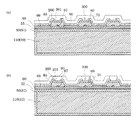
まず、図5(a)に示すように、流路形成基板10が複数一体的に形成されるシリコンウェハーである流路形成基板用ウェハー110の表面に弾性膜50を構成する二酸化シリコン(SiO)からなる二酸化シリコン膜51を形成する。次いで、図5(b)に示すように、弾性膜50(二酸化シリコン膜51)上に、例えば、酸化ジルコニウムからなる絶縁体膜55を形成する。 First, as shown in FIG. 5A, silicon dioxide (SiO 2) constituting an elastic film 50 on the surface of a flow path forming substrate wafer 110, which is a silicon wafer in which a plurality of flow path forming substrates 10 are integrally formed. ) Is formed. Next, as shown in FIG. 5B, an insulator film 55 made of, for example, zirconium oxide is formed on the elastic film 50 (silicon dioxide film 51).

次いで、図5(c)に示すように、白金からなる第1電極60を絶縁体膜55上に形成する。第1電極60の形成方法は特に限定されないが、例えば、スパッタリング法、化学蒸着法(CVD法)、物理蒸着法(PVD法)などが挙げられる。この第1電極60の材料は、特に限定されず、白金、イリジウム、これらの材料以外の金属又は金属酸化物を用いることができる。本実施形態のように圧電体層70としてチタン酸ジルコン酸鉛(PZT)を用いる場合には、酸化鉛の拡散による導電性の変化が少ない材料であることが望ましいため、第1電極60の材料としては白金、イリジウム等が好適に用いられる。   Next, as shown in FIG. 5C, a first electrode 60 made of platinum is formed on the insulator film 55. Although the formation method of the 1st electrode 60 is not specifically limited, For example, sputtering method, chemical vapor deposition method (CVD method), physical vapor deposition method (PVD method) etc. are mentioned. The material of the first electrode 60 is not particularly limited, and platinum, iridium, metals other than these materials, or metal oxides can be used. When lead zirconate titanate (PZT) is used as the piezoelectric layer 70 as in the present embodiment, it is desirable that the material has little change in conductivity due to diffusion of lead oxide. As platinum, iridium or the like is preferably used.

次に、図5(d)に示すように、補強部65、腕部66、及び第2の補強部67を構成するダイヤモンドライクカーボン(DLC)膜68を第1電極60上に形成する。ダイヤモンドライクカーボン膜68の成膜方法は特に限定されないが、例えば、真空蒸着、スパッタリング法、イオンプレーティング等の化学蒸着法(CVD法)、物理蒸着法(PVD法)などが挙げられる。なお、ダイヤモンドライクカーボン膜68の厚さは、本実施形態では50nmとした。   Next, as illustrated in FIG. 5D, a diamond-like carbon (DLC) film 68 that forms the reinforcing portion 65, the arm portion 66, and the second reinforcing portion 67 is formed on the first electrode 60. The method for forming the diamond-like carbon film 68 is not particularly limited, and examples thereof include chemical vapor deposition (CVD) such as vacuum vapor deposition, sputtering, and ion plating, and physical vapor deposition (PVD). Note that the thickness of the diamond-like carbon film 68 is 50 nm in the present embodiment.

そして、図6(a)に示すように、ダイヤモンドライクカーボン膜68をパターニングして、補強部65、腕部66、及び第2の補強部67を形成する。具体的には、圧電素子(図示なし)の幅方向中央部を残して、圧電素子に対向する領域を除去する。このとき、補強部65の圧力発生室(図示なし)側、及び第2の補強部67の端面が傾斜するようにする。ダイヤモンドライクカーボン膜68のパターニングは、ダイヤモンドライクカーボン膜68上にフォトリソグラフィー法により所定形状に形成したレジストを介してイオンミリング等のドライエッチングにより行う。   Then, as shown in FIG. 6A, the diamond-like carbon film 68 is patterned to form the reinforcing portion 65, the arm portion 66, and the second reinforcing portion 67. Specifically, the region facing the piezoelectric element is removed leaving the central portion in the width direction of the piezoelectric element (not shown). At this time, the pressure generating chamber (not shown) side of the reinforcing portion 65 and the end surface of the second reinforcing portion 67 are inclined. The diamond-like carbon film 68 is patterned by dry etching such as ion milling through a resist formed in a predetermined shape on the diamond-like carbon film 68 by a photolithography method.

次に、図6(b)に示すように、例えば、チタン酸ジルコン酸鉛(PZT)等からなる圧電体層70と、例えば、イリジウムからなる第2電極80とを流路形成基板用ウェハー110の全面に形成する。   Next, as shown in FIG. 6B, for example, a piezoelectric layer 70 made of lead zirconate titanate (PZT) or the like and a second electrode 80 made of iridium, for example, are used. On the entire surface.

なお、圧電素子300を構成する圧電体層70の材料としては、例えば、チタン酸ジルコン酸鉛(PZT)等の強誘電性圧電性材料や、これにニオブ、ニッケル、マグネシウム、ビスマス又はイットリウム等の金属を添加したリラクサ強誘電体等が用いられる。その組成は、圧電素子300の特性、用途等を考慮して適宜選択すればよい。また、圧電体層70の形成方法は、特に限定されないが、例えば、本実施形態では、金属有機物を溶媒に溶解・分散したいわゆるゾルを塗布乾燥してゲル化し、さらに高温で焼成することで金属酸化物からなる圧電体層70を得る、いわゆるゾル−ゲル法を用いて圧電体層70を形成した。なお、圧電体層70の形成方法は、ゾル−ゲル法に限定されず、例えば、MOD法やスパッタリング法などの薄膜形成方法を利用して圧電体層70を形成するようにしてもよい。実際には、圧電体層70は、上述したゾル−ゲル法により厚さの薄い圧電体膜を形成する工程を複数回繰り返し行って、複数層の圧電体膜からなる厚さ1300nmの圧電体層70を形成する。   The material of the piezoelectric layer 70 constituting the piezoelectric element 300 is, for example, a ferroelectric piezoelectric material such as lead zirconate titanate (PZT), or niobium, nickel, magnesium, bismuth, yttrium, or the like. A relaxor ferroelectric or the like to which a metal is added is used. The composition may be appropriately selected in consideration of the characteristics, usage, etc. of the piezoelectric element 300. The method for forming the piezoelectric layer 70 is not particularly limited. For example, in this embodiment, a so-called sol in which a metal organic material is dissolved and dispersed in a solvent is applied, dried, gelled, and further fired at a high temperature. The piezoelectric layer 70 was formed by using a so-called sol-gel method for obtaining a piezoelectric layer 70 made of an oxide. The method for forming the piezoelectric layer 70 is not limited to the sol-gel method. For example, the piezoelectric layer 70 may be formed using a thin film forming method such as a MOD method or a sputtering method. Actually, the piezoelectric layer 70 is formed by repeating the above-described process of forming a thin piezoelectric film by the sol-gel method a plurality of times, and a piezoelectric layer having a thickness of 1300 nm made up of a plurality of piezoelectric films. 70 is formed.

次に、図6(c)に示すように、圧電体層70及び第2電極80を、各圧力発生室12に対向する領域にパターニングして圧電素子300を形成する。圧電体層70及び第2電極80のパターニングは、フォトリソグラフィー法により第2電極80上に所定形状に形成したレジストを介してドライエッチングすることにより、一括して行うことができる。なお、圧電体層70を補強膜が露出されるまでエッチングすることにより実質的にエッチングが停止する。本実施形態では、補強膜が圧力発生室を並設方向に区画する隔壁に対応する領域にも設けられている、すなわち、第1電極60を覆うように設けられていることにより、第1電極60がオーバーエッチングされることがなく、第1電極60の膜厚のばらつきを抑制することができる。   Next, as shown in FIG. 6C, the piezoelectric layer 300 is formed by patterning the piezoelectric layer 70 and the second electrode 80 in regions facing the pressure generating chambers 12. Patterning of the piezoelectric layer 70 and the second electrode 80 can be performed collectively by dry etching through a resist formed in a predetermined shape on the second electrode 80 by photolithography. The etching is substantially stopped by etching the piezoelectric layer 70 until the reinforcing film is exposed. In the present embodiment, the reinforcing film is also provided in a region corresponding to the partition that partitions the pressure generating chambers in the juxtaposed direction, that is, the first electrode 60 is provided so as to cover the first electrode 60. 60 is not over-etched, and variations in the film thickness of the first electrode 60 can be suppressed.

次に、レジストを除去した後、図6(d)に示すように、流路形成基板用ウェハー110の全面に亘って被覆膜200を形成した後、被覆膜200を所定形状にパターニングすることにより、開口部201を形成する。このとき、図2に示す連通孔202を同時に形成する。   Next, after removing the resist, as shown in FIG. 6D, after forming the coating film 200 over the entire surface of the flow path forming substrate wafer 110, the coating film 200 is patterned into a predetermined shape. Thus, the opening 201 is formed. At this time, the communication hole 202 shown in FIG. 2 is formed at the same time.

次に、リード電極90を形成する。具体的には、図7(a)に示すように、流路形成基板用ウェハー110の全面に亘って、例えば、金(Au)等からなる金属膜を形成後、図7(b)に示すように、例えば、レジスト等からなるマスクパターン(図示なし)を介して各圧電素子300毎に金属膜をパターニングすることでリード電極90が形成される。   Next, the lead electrode 90 is formed. Specifically, as shown in FIG. 7A, a metal film made of, for example, gold (Au) or the like is formed over the entire surface of the flow path forming substrate wafer 110, and then shown in FIG. 7B. Thus, for example, the lead electrode 90 is formed by patterning the metal film for each piezoelectric element 300 through a mask pattern (not shown) made of a resist or the like.

そして、図示しないが、流路形成基板用ウェハー110の圧電素子300側に、シリコンウェハーであり複数の保護基板30となる保護基板用ウェハーを接着剤35によって接合する。なお、保護基板30には、リザーバー部31、圧電素子保持部32等が予め形成されている。また、保護基板30は、例えば、400μm程度の厚さを有するシリコン単結晶基板からなり、保護基板30を接合することで流路形成基板10の剛性は著しく向上することになる。その後、流路形成基板用ウェハー110を所定の厚さにする。   Although not shown, a protective substrate wafer that is a silicon wafer and serves as a plurality of protective substrates 30 is bonded to the piezoelectric element 300 side of the flow path forming substrate wafer 110 by an adhesive 35. The protective substrate 30 is preliminarily formed with a reservoir portion 31, a piezoelectric element holding portion 32, and the like. Further, the protective substrate 30 is made of, for example, a silicon single crystal substrate having a thickness of about 400 μm, and the rigidity of the flow path forming substrate 10 is remarkably improved by bonding the protective substrate 30. Thereafter, the flow path forming substrate wafer 110 is set to a predetermined thickness.

次いで、流路形成基板用ウェハー110にマスク膜を新たに形成し、所定形状にパターニングする。そして、流路形成基板用ウェハー110をマスク膜を介してKOH等のアルカリ溶液を用いた異方性エッチング(ウェットエッチング)することにより、圧電素子300に対応する圧力発生室12、連通部13、インク供給路14及び連通路15等を形成する。   Next, a mask film is newly formed on the flow path forming substrate wafer 110 and patterned into a predetermined shape. Then, by performing anisotropic etching (wet etching) using an alkaline solution such as KOH on the flow path forming substrate wafer 110 through the mask film, the pressure generating chamber 12 corresponding to the piezoelectric element 300, the communication portion 13, An ink supply path 14 and a communication path 15 are formed.

その後は、流路形成基板用ウェハー110の圧力発生室12が開口する面側のマスク膜を除去し、流路形成基板用ウェハー110及び保護基板用ウェハーの外周縁部の不要部分を、例えば、ダイシング等により切断することによって除去する。そして、流路形成基板用ウェハー110の保護基板用ウェハーとは反対側の面にノズル開口21が穿設されたノズルプレート20を接合すると共に、保護基板用ウェハーにコンプライアンス基板40を接合し、これら流路形成基板用ウェハー110等を、図1に示すような一つのチップサイズの流路形成基板10等に分割することによって上述した構造のインクジェット式記録ヘッドが製造される。   Thereafter, the mask film on the surface side where the pressure generation chamber 12 of the flow path forming substrate wafer 110 is opened is removed, and unnecessary portions of the outer peripheral edge portions of the flow path forming substrate wafer 110 and the protective substrate wafer are, for example, It is removed by cutting by dicing or the like. Then, the nozzle plate 20 having the nozzle openings 21 formed on the surface of the flow path forming substrate wafer 110 opposite to the protective substrate wafer is bonded, and the compliance substrate 40 is bonded to the protective substrate wafer. The ink jet recording head having the above-described structure is manufactured by dividing the flow path forming substrate wafer 110 and the like into a single chip size flow path forming substrate 10 as shown in FIG.

また、これらのインクジェット式記録ヘッド1は、インクカートリッジ等と連通するインク流路を具備する記録ヘッドユニットの一部を構成して、インクジェット式記録装置に搭載される。図8は、そのインクジェット式記録装置の概略構成を示す斜視図である。   Further, these ink jet recording heads 1 constitute a part of a recording head unit having an ink flow path communicating with an ink cartridge or the like, and are mounted on an ink jet recording apparatus. FIG. 8 is a perspective view showing a schematic configuration of the ink jet recording apparatus.

図8に示すように、本実施形態の液体噴射装置であるインクジェット式記録装置Iは、例えば、ブラック(B)、シアン(C)、マゼンダ(M)、イエロー(Y)等の複数の異なる色のインクが貯留される貯留室を有するインクカートリッジ(液体貯留手段)2が装着されたインクジェット式記録ヘッド1(以下、記録ヘッド)を具備する。記録ヘッド1はキャリッジ3に搭載されており、記録ヘッド1が搭載されたキャリッジ3は、装置本体4に取り付けられたキャリッジ軸5に軸方向移動自在に設けられている。そして、駆動モーター6の駆動力が図示しない複数の歯車およびタイミングベルト7を介してキャリッジ3に伝達されることで、キャリッジ3はキャリッジ軸5に沿って移動される。一方、装置本体4にはキャリッジ軸5に沿ってプラテン8が設けられており、図示しない給紙装置等により給紙された紙等の被記録媒体Sがプラテン8上を搬送されるようになっている。   As shown in FIG. 8, the ink jet recording apparatus I which is the liquid ejecting apparatus of the present embodiment has a plurality of different colors such as black (B), cyan (C), magenta (M), yellow (Y), and the like. An ink jet recording head 1 (hereinafter referred to as a recording head) to which an ink cartridge (liquid storing means) 2 having a storage chamber for storing the ink is mounted. The recording head 1 is mounted on a carriage 3, and the carriage 3 on which the recording head 1 is mounted is provided on a carriage shaft 5 attached to the apparatus body 4 so as to be movable in the axial direction. Then, the driving force of the driving motor 6 is transmitted to the carriage 3 through a plurality of gears and a timing belt 7 (not shown), so that the carriage 3 is moved along the carriage shaft 5. On the other hand, the apparatus body 4 is provided with a platen 8 along the carriage shaft 5, so that a recording medium S such as paper fed by a paper feeding device (not shown) is conveyed on the platen 8. ing.

(実施形態2)
図9は、実施形態2に係る記録ヘッドの圧電素子及び圧力発生室の要部断面図である。本実施形態は、補強膜の形状以外は、実施形態1と同様であるので、同一作用を示す部分には同一符号を付して重複する説明は省略する。
(Embodiment 2)
FIG. 9 is a cross-sectional view of main parts of the piezoelectric element and the pressure generation chamber of the recording head according to the second embodiment. Since the present embodiment is the same as the first embodiment except for the shape of the reinforcing membrane, the same reference numerals are given to the portions showing the same action, and redundant description is omitted.

図9に示すように、第1電極60上であって、圧電素子300の幅方向における圧電体層70の両端部に対応する領域には、第1電極60を形成する膜よりも硬い材料からなる補強部65Aが設けられている。そして、この補強部65Aから連続して圧電素子300の幅方向外側に腕部66Aが延設されている。このように補強部65Aと腕部66Aは一体であり、補強膜を構成している。また、補強部65Aは、圧電素子300の幅方向内側に向かって厚さが漸小している。そして、腕部66Aは、補強部65Aよりも厚さが薄くなっている。   As shown in FIG. 9, the region on the first electrode 60 corresponding to both end portions of the piezoelectric layer 70 in the width direction of the piezoelectric element 300 is made of a material harder than the film forming the first electrode 60. A reinforcing portion 65A is provided. An arm portion 66A extends continuously from the reinforcing portion 65A to the outer side in the width direction of the piezoelectric element 300. In this way, the reinforcing portion 65A and the arm portion 66A are integrated to constitute a reinforcing film. Further, the thickness of the reinforcing portion 65A gradually decreases toward the inner side in the width direction of the piezoelectric element 300. The arm portion 66A is thinner than the reinforcing portion 65A.

また、第1電極60上であって圧電素子300の幅方向中央部には、第1電極60を形成する膜よりも硬い材料からなる第2の補強部67が圧力発生室12の長手方向に亘って設けられている。   Further, a second reinforcing portion 67 made of a material harder than the film forming the first electrode 60 is provided in the longitudinal direction of the pressure generating chamber 12 on the first electrode 60 and in the central portion in the width direction of the piezoelectric element 300. It is provided over.

このように、補強膜の腕部66Aを薄くすることにより、実施形態1よりも振動板の拘束力を減少させることができ、実施形態1と比較して振動板の変位量を向上させることができる。   Thus, by making the arm portion 66A of the reinforcing film thinner, the restraining force of the diaphragm can be reduced than in the first embodiment, and the displacement amount of the diaphragm can be improved as compared with the first embodiment. it can.

補強部65Aを設けることにより、圧電素子300の幅方向端部における応力集中に対する第1電極60の剛性が高くなり駆動耐久性を向上させることができると共に、変位特性に優れたものとすることができる。また、圧電素子300の幅方向端部における応力を分散させて、第1電極60への応力集中を抑制することができる。また、第2の補強部67を設けることにより、圧電素子300の長手方向の駆動耐久性を向上させることができる。また、補強膜の腕部66Aがエッチングストップ層として機能し、第1電極60がエッチングされることがない。したがって、第1電極60の膜厚のばらつきを抑制することができる。   By providing the reinforcing portion 65A, the rigidity of the first electrode 60 with respect to the stress concentration at the end in the width direction of the piezoelectric element 300 can be increased, driving durability can be improved, and displacement characteristics can be improved. it can. In addition, the stress concentration at the first electrode 60 can be suppressed by dispersing the stress at the end in the width direction of the piezoelectric element 300. Further, by providing the second reinforcing portion 67, the driving durability in the longitudinal direction of the piezoelectric element 300 can be improved. Further, the arm portion 66A of the reinforcing film functions as an etching stop layer, and the first electrode 60 is not etched. Therefore, variations in the film thickness of the first electrode 60 can be suppressed.

本実施形態の補強膜の製造方法は特に限定されないが、例えば、圧電体層70及び第2電極80をパターニングする際に、補強膜の厚さが半分になるまでエッチングを行うことにより、腕部66Aを形成することができる。   The method of manufacturing the reinforcing film according to the present embodiment is not particularly limited. For example, when patterning the piezoelectric layer 70 and the second electrode 80, etching is performed until the thickness of the reinforcing film is reduced to half. 66A can be formed.

(実施形態3)
図10は、実施形態3に係る記録ヘッドの圧電素子及び圧力発生室の要部断面図である。本実施形態は、補強膜の形状以外は、実施形態1と同様であるので、同一作用を示す部分には同一符号を付して重複する説明は省略する。
(Embodiment 3)
FIG. 10 is a cross-sectional view of main parts of the piezoelectric element and the pressure generation chamber of the recording head according to the third embodiment. Since the present embodiment is the same as the first embodiment except for the shape of the reinforcing membrane, the same reference numerals are given to the portions showing the same action, and redundant description is omitted.

図10に示すように、第1電極60上であって、圧電素子300の幅方向における圧電体層70の両端部に対応する領域には、第1電極60を形成する膜よりも硬い材料からなる補強部65Bが設けられている。本実施形態では、圧電素子300の幅方向における圧電体層70の両端部に対応する領域に補強部65Bを設け、腕部を設けていない。補強部65Bは、第1電極60と圧電体層70との間に設けられて、圧電素子300の幅方向内側に向かって厚さが漸小している。また、かかる補強部65Bは、圧電素子300の幅方向外側に向かって厚さが漸小している。このような構成とすることにより、振動板の拘束力を実施形態2よりもさらに減少させることができ、変位量を向上させることができる。すなわち、変位特性がさらに優れたものとすることができる。   As shown in FIG. 10, the region on the first electrode 60 corresponding to both end portions of the piezoelectric layer 70 in the width direction of the piezoelectric element 300 is made of a material harder than the film forming the first electrode 60. The reinforcement part 65B which becomes is provided. In the present embodiment, the reinforcing portion 65B is provided in a region corresponding to both ends of the piezoelectric layer 70 in the width direction of the piezoelectric element 300, and no arm portion is provided. The reinforcing portion 65 </ b> B is provided between the first electrode 60 and the piezoelectric layer 70, and the thickness gradually decreases toward the inner side in the width direction of the piezoelectric element 300. In addition, the thickness of the reinforcing portion 65 </ b> B gradually decreases toward the outer side in the width direction of the piezoelectric element 300. By setting it as such a structure, the restraining force of a diaphragm can further be reduced rather than Embodiment 2, and the amount of displacement can be improved. That is, the displacement characteristics can be further improved.

また、第1電極60上であって圧電素子300の幅方向中央部には、第1電極60を形成する膜よりも硬い材料からなる第2の補強部67が圧力発生室12の長手方向に亘って設けられている。   Further, a second reinforcing portion 67 made of a material harder than the film forming the first electrode 60 is provided in the longitudinal direction of the pressure generating chamber 12 on the first electrode 60 and in the central portion in the width direction of the piezoelectric element 300. It is provided over.

補強部65Bを設けることにより、圧電素子300の幅方向端部における応力集中に対する第1電極60の剛性が高くなり、圧電素子300の駆動耐久性を向上させることができる。また、圧電素子300の幅方向端部における応力を分散させて、第1電極60への応力集中を抑制することができる。また、第2の補強部67を設けることにより、圧電素子300の長手方向の駆動耐久性を向上させることができる。   By providing the reinforcing portion 65B, the rigidity of the first electrode 60 with respect to the stress concentration at the end in the width direction of the piezoelectric element 300 is increased, and the driving durability of the piezoelectric element 300 can be improved. In addition, the stress concentration at the first electrode 60 can be suppressed by dispersing the stress at the end in the width direction of the piezoelectric element 300. Further, by providing the second reinforcing portion 67, the driving durability in the longitudinal direction of the piezoelectric element 300 can be improved.

本実施形態の補強部65Bの製造方法は特に限定されないが、例えば、圧電体層70及び第2電極80をパターニングする際に、同時に補強部65Bを構成するダイヤモンドライクカーボン膜もパターニングして、第1電極60が露出するようにすればよい。   The manufacturing method of the reinforcing portion 65B of the present embodiment is not particularly limited. For example, when the piezoelectric layer 70 and the second electrode 80 are patterned, the diamond-like carbon film constituting the reinforcing portion 65B is also patterned, One electrode 60 may be exposed.

(実施形態4)
図11は、実施形態4に係る記録ヘッドの圧電素子及び圧力発生室の要部断面図である。本実施形態は、補強膜の形状以外は、実施形態1と同様であるので、同一作用を示す部分には同一符号を付して重複する説明は省略する。
(Embodiment 4)
FIG. 11 is a cross-sectional view of main parts of the piezoelectric element and the pressure generation chamber of the recording head according to the fourth embodiment. Since the present embodiment is the same as the first embodiment except for the shape of the reinforcing membrane, the same reference numerals are given to the portions showing the same action, and redundant description is omitted.

図11に示すように、第1電極60上であって、圧電素子300の幅方向における圧電体層70の両端部に対応する領域には、第1電極60を形成する膜よりも硬い材料からなる補強部65Cが設けられている。そして、この補強部65Cから連続して圧電素子300の幅方向外側に腕部66Cが延設されている。このように補強部65Cと腕部66Cは一体であり、補強膜を構成している。すなわち、補強膜は、第1電極60と圧電体層70との間に設けられている補強部65Cと、補強部から連続して圧電素子300の幅方向外側に延設する腕部66Cとからなる。また、補強部65Cは、圧電素子300の幅方向内側に向かって厚さが漸小している。そして、補強膜は、補強部65Cと腕部66Cの境界部分に凹部が設けられている。この凹部は、その内面が曲面状に設けられている。   As shown in FIG. 11, the region on the first electrode 60 corresponding to both end portions of the piezoelectric layer 70 in the width direction of the piezoelectric element 300 is made of a material harder than the film forming the first electrode 60. A reinforcing portion 65C is provided. And the arm part 66C is continuously extended from the reinforcement part 65C on the width direction outer side of the piezoelectric element 300. In this way, the reinforcing portion 65C and the arm portion 66C are integrated to form a reinforcing film. That is, the reinforcing film is composed of a reinforcing portion 65C provided between the first electrode 60 and the piezoelectric layer 70, and an arm portion 66C that extends continuously outward from the piezoelectric element 300 in the width direction. Become. Further, the thickness of the reinforcing portion 65C gradually decreases toward the inner side in the width direction of the piezoelectric element 300. The reinforcing film is provided with a recess at a boundary portion between the reinforcing portion 65C and the arm portion 66C. The recess has a curved inner surface.

また、第1電極60上であって圧電素子300の幅方向中央部には、第1電極60を形成する膜よりも硬い材料からなる第2の補強部67が圧力発生室12の長手方向に亘って設けられている。   Further, a second reinforcing portion 67 made of a material harder than the film forming the first electrode 60 is provided in the longitudinal direction of the pressure generating chamber 12 on the first electrode 60 and in the central portion in the width direction of the piezoelectric element 300. It is provided over.

このように、圧電体層70に対応する領域との境界部分に凹部が設けられており、且つ該凹部の内面が曲面状となっていることにより、圧電素子300の幅方向端部における振動板への応力をさらに効果的に分散させることができる。これにより、第1電極60を含む振動板の破壊がさらに抑制されて、圧電素子300の駆動耐久性をより向上させることができる。   As described above, the concave portion is provided at the boundary portion with the region corresponding to the piezoelectric layer 70, and the inner surface of the concave portion has a curved surface, so that the diaphragm at the end portion in the width direction of the piezoelectric element 300 is provided. Can be more effectively dispersed. Thereby, destruction of the diaphragm including the first electrode 60 is further suppressed, and the driving durability of the piezoelectric element 300 can be further improved.

さらに、本実施形態では、凹部の内面を曲面状に形成したため、被覆膜200の補強膜上への付きまわりを向上して、被覆膜200によって圧電素子300を確実に保護して、圧電素子300が破壊されるのを確実に防止することができる。   Furthermore, in this embodiment, since the inner surface of the concave portion is formed in a curved surface shape, the covering of the coating film 200 on the reinforcing film is improved, and the piezoelectric element 300 is reliably protected by the coating film 200, so It is possible to reliably prevent the element 300 from being destroyed.

補強部65Cを設けることにより、圧電素子300の幅方向端部における応力集中に対する第1電極60の剛性が高くなり、駆動耐久性を向上させることができる。また、第2の補強部67を設けることにより、圧電素子300の長手方向の駆動耐久性を向上させることができる。また、補強膜の腕部66Cがエッチングストップ層として機能し、第1電極60がエッチングされることがない。したがって、第1電極60の膜厚のばらつきを抑制することができる。   By providing the reinforcing portion 65C, the rigidity of the first electrode 60 with respect to the stress concentration at the end portion in the width direction of the piezoelectric element 300 is increased, and driving durability can be improved. Further, by providing the second reinforcing portion 67, the driving durability in the longitudinal direction of the piezoelectric element 300 can be improved. Further, the arm portion 66C of the reinforcing film functions as an etching stop layer, and the first electrode 60 is not etched. Therefore, variations in the film thickness of the first electrode 60 can be suppressed.

さらに、本実施形態では、凹部の内面を曲面状に設けるようにしたため、また、圧電素子300の幅方向端部における応力をさらに効果的に分散させて、第1電極60への応力集中をさらに抑制することができる。これにより、駆動耐久性をさらに向上させることができる。   Furthermore, in the present embodiment, the inner surface of the concave portion is provided in a curved shape, and moreover, stress at the end in the width direction of the piezoelectric element 300 is further effectively distributed, and stress concentration on the first electrode 60 is further increased. Can be suppressed. Thereby, driving durability can be further improved.

本実施形態の補強膜の製造方法は特に限定されないが、例えば、圧電体層70及び第2電極80をパターニングする際に、同時に補強膜に至るまでドライエッチングすることで、補強膜の補強部65Cと腕部66Cとの境界部分に凹部を形成する。このような凹部は、ドライエッチングする際の電圧、温度等を適宜変更することで積極的に形成することができる。   The method for manufacturing the reinforcing film of the present embodiment is not particularly limited. For example, when patterning the piezoelectric layer 70 and the second electrode 80, dry etching is performed until the reinforcing film reaches the reinforcing film at the same time, thereby reinforcing the reinforcing part 65C of the reinforcing film. A recess is formed at the boundary between the arm portion 66C and the arm portion 66C. Such a recess can be positively formed by appropriately changing the voltage, temperature, etc. during dry etching.

(他の実施形態)
以上、本発明の実施形態について説明したが、本発明は、上述の実施形態に限定されるものではない。例えば、上述した実施形態では、流路形成基板10としてシリコン単結晶基板を例示したが、特にこれに限定されず、例えば、SOI基板、ガラス基板、MgO基板等においても本発明は有効である。また、振動板の最下層に二酸化シリコンからなる弾性膜50を設けるようにしたが、振動板の構成は、特にこれに限定されるものではない。
上述した実施形態では、被覆膜200を設けたが、設けなくてもよい。
また、実施形態1〜4では、第2の補強部67を設けたがいずれも設けなくてもよい。
(Other embodiments)
As mentioned above, although embodiment of this invention was described, this invention is not limited to the above-mentioned embodiment. For example, in the above-described embodiment, a silicon single crystal substrate is exemplified as the flow path forming substrate 10, but the present invention is not limited to this, and the present invention is also effective for an SOI substrate, a glass substrate, an MgO substrate, and the like. Further, the elastic film 50 made of silicon dioxide is provided in the lowermost layer of the diaphragm, but the structure of the diaphragm is not particularly limited to this.
In the embodiment described above, the coating film 200 is provided, but it may not be provided.
In the first to fourth embodiments, the second reinforcing portion 67 is provided, but none of them may be provided.

また、上述したインクジェット式記録装置Iでは、インクジェット式記録ヘッド1がキャリッジ3に搭載されて主走査方向に移動するものを例示したが、特にこれに限定されず、例えば、インクジェット式記録ヘッド1が固定されて、紙等の記録シートSを副走査方向に移動させるだけで印刷を行う、所謂ライン式記録装置にも本発明を適用することができる。   In the ink jet recording apparatus I described above, the ink jet recording head 1 is mounted on the carriage 3 and moves in the main scanning direction. However, the present invention is not particularly limited thereto. The present invention can also be applied to a so-called line type recording apparatus in which printing is performed simply by moving a recording sheet S such as paper in the sub-scanning direction.

なお、上述の実施形態では、液体噴射ヘッドの一例としてインクジェット式記録ヘッドを挙げて説明したが、本発明は広く液体噴射ヘッド全般を対象としたものであり、インク以外の液体を噴射する液体噴射ヘッドにも勿論適用することができる。その他の液体噴射ヘッドとしては、例えば、プリンター等の画像記録装置に用いられる各種の記録ヘッド、液晶ディスプレー等のカラーフィルターの製造に用いられる色材噴射ヘッド、有機ELディスプレー、FED(電界放出ディスプレー)等の電極形成に用いられる電極材料噴射ヘッド、バイオchip製造に用いられる生体有機物噴射ヘッド等が挙げられる。   In the above-described embodiment, the ink jet recording head has been described as an example of the liquid ejecting head. However, the present invention is widely applied to all liquid ejecting heads, and the liquid ejecting ejects liquids other than ink. Of course, it can also be applied to the head. Other liquid ejecting heads include, for example, various recording heads used in image recording apparatuses such as printers, color material ejecting heads used in the manufacture of color filters such as liquid crystal displays, organic EL displays, and FEDs (field emission displays). Examples thereof include an electrode material ejection head used for electrode formation, a bioorganic matter ejection head used for biochip production, and the like.

また、本発明は、インクジェット式記録ヘッドに代表される液体噴射ヘッドに搭載される圧電素子に限られず、他の装置に搭載される圧電素子にも適用することができる。   The present invention is not limited to a piezoelectric element mounted on a liquid jet head typified by an ink jet recording head, and can also be applied to a piezoelectric element mounted on another apparatus.

1 インクジェット式記録ヘッド(液体噴射ヘッド)、 10 流路形成基板、 12 圧力発生室、 13 連通部、 14 インク供給路、 15 連通路、 20 ノズルプレート、 21 ノズル開口、 30 保護基板、 31 リザーバー部、 32 圧電素子保持部、 40 コンプライアンス基板、 60 第1電極、 65 補強部、 66 腕部、 67 第2の補強部、 70 圧電体層、 80 第2電極、 90 リード電極、 100 リザーバー、 120 駆動回路、 121 接続配線、 300 圧電素子 DESCRIPTION OF SYMBOLS 1 Inkjet recording head (liquid ejecting head), 10 Flow path formation board | substrate, 12 Pressure generation chamber, 13 Communication part, 14 Ink supply path, 15 Communication path, 20 Nozzle plate, 21 Nozzle opening, 30 Protection board, 31 Reservoir part , 32 piezoelectric element holding part, 40 compliance substrate, 60 first electrode, 65 reinforcing part, 66 arm part, 67 second reinforcing part, 70 piezoelectric layer, 80 second electrode, 90 lead electrode, 100 reservoir, 120 driving Circuit, 121 connection wiring, 300 piezoelectric element

Claims (10)

液体を噴射するノズル開口に連通する圧力発生室が並設された流路形成基板と、
前記流路形成基板上に設けられた第1電極前記第1電極上に設けられた圧電体層及び前記圧電体層上に設けられた第2電極具備し、各圧力発生室に対応する圧電素子と、
を備え、
前記圧電素子は、前記圧力発生室の並設方向に沿った幅を持ち、前記第1電極上であって、前記圧電素子の幅方向における前記圧電体層の両端部に対応する領域、前記第1電極を形成する膜よりも硬い材料からなる補強部を有し、
前記補強部は、前記圧電素子の幅方向内側に向かって厚さが漸小することを特徴とする液体噴射ヘッド。
A flow path forming substrate in which pressure generation chambers communicating with nozzle openings for ejecting liquid are arranged in parallel ;
Comprising a second electrode provided on the channel forming a first electrode provided on the substrate, a piezoelectric layer provided on the first electrode and the piezoelectric layer, corresponding to the pressure generating chambers A piezoelectric element;
With
The piezoelectric element has a width along the arrangement direction of the pressure generating chamber, a on the first electrode, in a region corresponding to both end portions of the piezoelectric layer in the width direction of the piezoelectric element, wherein Having a reinforcing part made of a material harder than the film forming the first electrode ;
The liquid ejecting head according to claim 1, wherein the reinforcing portion gradually decreases in thickness toward an inner side in the width direction of the piezoelectric element.
前記補強部は、ビッカース硬度Hvが1000以上の材料からなることを特徴とする請求項1に記載の液体噴射ヘッド。   The liquid ejecting head according to claim 1, wherein the reinforcing portion is made of a material having a Vickers hardness Hv of 1000 or more. 前記補強部から連続して前記圧電素子の幅方向外側に延設される腕部を具備することを特徴とする請求項1又は2に記載の液体噴射ヘッド。   3. The liquid ejecting head according to claim 1, further comprising an arm portion extending continuously outward from the reinforcing portion in the width direction of the piezoelectric element. 前記腕部は、前記補強部よりも厚さが薄いことを特徴とする請求項3に記載の液体噴射ヘッド。   The liquid ejecting head according to claim 3, wherein the arm portion is thinner than the reinforcing portion. 前記補強部と前記腕部の境界部分には凹部が設けられており、且つ該凹部の内面が曲面状となっていることを特徴とする請求項3又は4に記載の液体噴射ヘッド。   The liquid ejecting head according to claim 3, wherein a concave portion is provided at a boundary portion between the reinforcing portion and the arm portion, and an inner surface of the concave portion is curved. 前記第1電極上であって前記圧電素子の幅方向中央部には、前記第1電極を形成する膜よりも硬い材料からなる第2の補強部が前記圧力発生室の長手方向に亘って設けられていることを特徴とする請求項1〜5のいずれか一項に記載の液体噴射ヘッド。   A second reinforcing portion made of a material harder than the film forming the first electrode is provided in the longitudinal direction of the pressure generating chamber on the first electrode and in the center in the width direction of the piezoelectric element. The liquid ejecting head according to claim 1, wherein the liquid ejecting head is provided. 前記第2の補強部は、前記圧電素子の幅方向外側に向かって厚さが漸小することを特徴とする請求項6に記載の液体噴射ヘッド。 The liquid ejecting head according to claim 6, wherein the thickness of the second reinforcing portion gradually decreases toward the outer side in the width direction of the piezoelectric element. 少なくとも前記圧電体層の側面を覆う絶縁体からなる被覆膜が設けられていることを特徴とする請求項1〜7のいずれか一項に記載の液体噴射ヘッド。   The liquid ejecting head according to claim 1, wherein a coating film made of an insulator that covers at least a side surface of the piezoelectric layer is provided. 請求項1〜8のいずれか一項に記載の液体噴射ヘッドを具備することを特徴とする液体噴射装置。   A liquid ejecting apparatus comprising the liquid ejecting head according to claim 1. 基板上に設けられた第1電極と、前記第1電極上に設けられた圧電体層と、前記圧電体層上に設けられた第2電極とを具備する圧電素子を備え、
前記第1電極上であって、前記圧電素子の幅方向における前記圧電体層の両端部に対応する領域には、前記第1電極を形成する膜よりも硬い材料からなる補強部が設けられ、
前記補強部は、前記圧電素子の幅方向内側に向かって厚さが漸小することを特徴とするアクチュエーター装置。
A piezoelectric element comprising: a first electrode provided on a substrate; a piezoelectric layer provided on the first electrode; and a second electrode provided on the piezoelectric layer;
On the first electrode, a region corresponding to both end portions of the piezoelectric layer in the width direction of the piezoelectric element is provided with a reinforcing portion made of a material harder than the film forming the first electrode,
The said reinforcement part is an actuator apparatus characterized by the thickness decreasing gradually toward the width direction inner side of the said piezoelectric element.
JP2009183904A 2009-03-26 2009-08-06 Liquid ejecting head, liquid ejecting apparatus, and actuator device Expired - Fee Related JP5321832B2 (en)

Priority Applications (1)

Application Number Priority Date Filing Date Title
JP2009183904A JP5321832B2 (en) 2009-03-26 2009-08-06 Liquid ejecting head, liquid ejecting apparatus, and actuator device

Applications Claiming Priority (3)

Application Number Priority Date Filing Date Title
JP2009077863 2009-03-26
JP2009183904A JP5321832B2 (en) 2009-03-26 2009-08-06 Liquid ejecting head, liquid ejecting apparatus, and actuator device

Publications (3)

Publication Number Publication Date
JP2010247511A JP2010247511A (en) 2010-11-04
JP2010247511A5 JP2010247511A5 (en) 2012-09-20
JP5321832B2 true JP5321832B2 (en) 2013-10-23

Family

ID=43310419

Family Applications (1)

Application Number Title Priority Date Filing Date
JP2009183904A Expired - Fee Related JP5321832B2 (en) 2009-03-26 2009-08-06 Liquid ejecting head, liquid ejecting apparatus, and actuator device

Country Status (1)

Country Link
JP (1) JP5321832B2 (en)

Families Citing this family (3)

* Cited by examiner, † Cited by third party
Publication number Priority date Publication date Assignee Title
JP5644581B2 (en) * 2011-02-22 2014-12-24 株式会社リコー Inkjet head and inkjet recording apparatus
US8585183B2 (en) * 2011-03-22 2013-11-19 Xerox Corporation High density multilayer interconnect for print head
JP2013146882A (en) * 2012-01-18 2013-08-01 Seiko Epson Corp Liquid ejection head and liquid ejecting apparatus

Family Cites Families (3)

* Cited by examiner, † Cited by third party
Publication number Priority date Publication date Assignee Title
JP4265576B2 (en) * 2004-06-29 2009-05-20 ブラザー工業株式会社 Liquid transfer device
JP2007195316A (en) * 2006-01-18 2007-08-02 Seiko Epson Corp Actuator device, manufacturing method therefor, and liquid injection head
JP2009029012A (en) * 2007-07-26 2009-02-12 Seiko Epson Corp Liquid jetting head and liquid jet apparatus

Also Published As

Publication number Publication date
JP2010247511A (en) 2010-11-04

Similar Documents

Publication Publication Date Title
JP3726909B2 (en) Method for manufacturing liquid jet head
JP4450238B2 (en) Liquid ejecting head and liquid ejecting apparatus
JP2008010528A (en) Actuator device, liquid injection head, and liquid injection apparatus
US20090289999A1 (en) Liquid ejecting head and liquid ejecting apparatus including the same
JP2006231909A (en) Liquid jetting head and liquid jetting apparatus
US8579417B2 (en) Liquid ejecting head, liquid ejecting apparatus, actuator device, and manufacturing method of liquid ejecting head
JP4614068B2 (en) Liquid ejecting head, manufacturing method thereof, and liquid ejecting apparatus
JP5737535B2 (en) Liquid ejecting head and liquid ejecting apparatus
JP2006255972A (en) Liquid jetting head, and liquid jetting device
JP5999301B2 (en) Piezoelectric element, liquid ejecting head, and liquid ejecting apparatus
JP4848919B2 (en) Liquid ejecting head and liquid ejecting apparatus
JP5321832B2 (en) Liquid ejecting head, liquid ejecting apparatus, and actuator device
JP2010131881A (en) Actuator device, liquid jet head, and liquid jet device
JP5382323B2 (en) Liquid ejecting head and liquid ejecting apparatus
JP4068784B2 (en) Inkjet recording head and inkjet recording apparatus
US7591544B2 (en) Liquid ejecting head, method of producing the same, and liquid ejecting apparatus
JP4457649B2 (en) Liquid ejecting head and liquid ejecting apparatus
JP2010253786A (en) Liquid ejection head, liquid ejector, and actuator device
JP2005178293A (en) Liquid jet head and liquid jet device
JP5447786B2 (en) Liquid ejecting head, liquid ejecting apparatus, and actuator device
JP2012218188A (en) Manufacturing method of liquid jet head
JP2005119199A (en) Liquid jetting head and liquid jetting apparatus
JP2010228274A (en) Liquid jetting head and liquid jetting device
JP3882915B2 (en) Liquid ejecting head, manufacturing method thereof, and liquid ejecting apparatus
JP5382324B2 (en) Liquid ejecting head and liquid ejecting apparatus

Legal Events

Date Code Title Description
A521 Written amendment

Free format text: JAPANESE INTERMEDIATE CODE: A523

Effective date: 20120806

A621 Written request for application examination

Free format text: JAPANESE INTERMEDIATE CODE: A621

Effective date: 20120806

TRDD Decision of grant or rejection written
A01 Written decision to grant a patent or to grant a registration (utility model)

Free format text: JAPANESE INTERMEDIATE CODE: A01

Effective date: 20130619

A61 First payment of annual fees (during grant procedure)

Free format text: JAPANESE INTERMEDIATE CODE: A61

Effective date: 20130702

R150 Certificate of patent or registration of utility model

Free format text: JAPANESE INTERMEDIATE CODE: R150

S531 Written request for registration of change of domicile

Free format text: JAPANESE INTERMEDIATE CODE: R313531

R350 Written notification of registration of transfer

Free format text: JAPANESE INTERMEDIATE CODE: R350

LAPS Cancellation because of no payment of annual fees