JP5313771B2 - Output circuit including pre-emphasis function - Google Patents
Output circuit including pre-emphasis function Download PDFInfo
- Publication number
- JP5313771B2 JP5313771B2 JP2009133225A JP2009133225A JP5313771B2 JP 5313771 B2 JP5313771 B2 JP 5313771B2 JP 2009133225 A JP2009133225 A JP 2009133225A JP 2009133225 A JP2009133225 A JP 2009133225A JP 5313771 B2 JP5313771 B2 JP 5313771B2
- Authority
- JP
- Japan
- Prior art keywords
- differential
- output
- output terminal
- turned
- emphasis
- Prior art date
- Legal status (The legal status is an assumption and is not a legal conclusion. Google has not performed a legal analysis and makes no representation as to the accuracy of the status listed.)
- Expired - Fee Related
Links
Images


Classifications
-
- H—ELECTRICITY
- H03—ELECTRONIC CIRCUITRY
- H03K—PULSE TECHNIQUE
- H03K19/00—Logic circuits, i.e. having at least two inputs acting on one output; Inverting circuits
- H03K19/01—Modifications for accelerating switching
- H03K19/017—Modifications for accelerating switching in field-effect transistor circuits
- H03K19/01707—Modifications for accelerating switching in field-effect transistor circuits in asynchronous circuits
- H03K19/01721—Modifications for accelerating switching in field-effect transistor circuits in asynchronous circuits by means of a pull-up or down element
-
- H—ELECTRICITY
- H03—ELECTRONIC CIRCUITRY
- H03K—PULSE TECHNIQUE
- H03K19/00—Logic circuits, i.e. having at least two inputs acting on one output; Inverting circuits
- H03K19/0175—Coupling arrangements; Interface arrangements
- H03K19/0185—Coupling arrangements; Interface arrangements using field effect transistors only
- H03K19/018557—Coupling arrangements; Impedance matching circuits
- H03K19/018564—Coupling arrangements; Impedance matching circuits with at least one differential stage
-
- H—ELECTRICITY
- H04—ELECTRIC COMMUNICATION TECHNIQUE
- H04L—TRANSMISSION OF DIGITAL INFORMATION, e.g. TELEGRAPHIC COMMUNICATION
- H04L25/00—Baseband systems
- H04L25/02—Details ; arrangements for supplying electrical power along data transmission lines
- H04L25/0264—Arrangements for coupling to transmission lines
- H04L25/0272—Arrangements for coupling to multiple lines, e.g. for differential transmission
-
- H—ELECTRICITY
- H04—ELECTRIC COMMUNICATION TECHNIQUE
- H04L—TRANSMISSION OF DIGITAL INFORMATION, e.g. TELEGRAPHIC COMMUNICATION
- H04L25/00—Baseband systems
- H04L25/02—Details ; arrangements for supplying electrical power along data transmission lines
- H04L25/03—Shaping networks in transmitter or receiver, e.g. adaptive shaping networks
- H04L25/03006—Arrangements for removing intersymbol interference
- H04L25/03343—Arrangements at the transmitter end
-
- H—ELECTRICITY
- H04—ELECTRIC COMMUNICATION TECHNIQUE
- H04L—TRANSMISSION OF DIGITAL INFORMATION, e.g. TELEGRAPHIC COMMUNICATION
- H04L25/00—Baseband systems
- H04L25/02—Details ; arrangements for supplying electrical power along data transmission lines
- H04L25/03—Shaping networks in transmitter or receiver, e.g. adaptive shaping networks
- H04L25/03878—Line equalisers; line build-out devices
Description
本発明は、プリエンファシス機能を含む出力回路に関する。 The present invention relates to an output circuit including a pre-emphasis function.
自集積回路の信号を他集積回路へ差動伝送路を介して送信する差動の出力回路において、伝送路での損失等を考慮してプリエンファシス(Pre−Emphasis)をかけて伝送するのが一般的である。プリエンファシス機能を有する出力回路では出力する現在のビットデータが直前に出力したビットデータから変化した時に、プリエンファシスをかけ、変化無しのときはプリエンファシスをかけない。 In a differential output circuit that transmits a signal of a self-integrated circuit to another integrated circuit via a differential transmission path, transmission is performed with pre-emphasis in consideration of a loss in the transmission path. It is common. In an output circuit having a pre-emphasis function, pre-emphasis is applied when the current bit data to be output changes from the bit data output immediately before, and pre-emphasis is not applied when there is no change.
プリエンファシス機能を有する差動出力回路において、直前のビットデータの値から遷移しプリエンファシスがかかったビットであるトランジション・ビット(Transition bit)と、プリエンファシスがかかっていないビットであるデエンファシス・ビット(De−emphasis bit)間で、差動出力信号の中点電圧であるコモンモード電圧(VCM)に不一致が生じる場合がある。トランジション・ビットとデエンファシス・ビット間でコモンモード電圧(VCM)の変動が大きいと、例えばPCI−Express/Serial−ATA/CEI等の標準インターフェース規格を逸脱する可能性がある。図11に、標準インターフェース規格のACコモンモード電圧(Vcmac;AC coupled common mode voltage(AC結合コモンモード電圧))の仕様の一例を示す。これらの標準インターフェース規格に対応した出力回路は、低消費電力化のために低電源電圧での動作が要求される。低電源電圧でPCI−Expressのように大きな差動出力振幅(800mV以上、1200mV以下)を実現しようとしたとき、トランジション・ビットとデエンファシス・ビット間でのコモンモード電圧(VCM)の不一致によるコモンモード電圧(VCM)の変動が大きくなる傾向にある。このため、コモンモード電圧(VCM)の変動の低減、抑制の必要性が増してくる。以下では、プリエンファシス機能を備えた出力回路(VCMの変動抑制機能無し)と、VCMの変動抑制機能を備えた出力回路の関連技術について順次説明を行う。 In a differential output circuit having a pre-emphasis function, a transition bit (Transition bit) that is a bit that has undergone pre-emphasis after a transition from the previous bit data value, and a de-emphasis bit that is a bit that has not been pre-emphasized There may be a mismatch in the common mode voltage (VCM), which is the midpoint voltage of the differential output signal, between (De-emphasis bits). If the variation of the common mode voltage (VCM) between the transition bit and the de-emphasis bit is large, there is a possibility of deviating from a standard interface standard such as PCI-Express / Serial-ATA / CEI. FIG. 11 shows an example of the specification of the AC common mode voltage (Vcmac; AC coupled common mode voltage) of the standard interface standard. An output circuit corresponding to these standard interface standards is required to operate at a low power supply voltage in order to reduce power consumption. Common due to mismatch of common mode voltage (VCM) between transition bit and de-emphasis bit when trying to realize large differential output amplitude (800mV or more, 1200mV or less) like PCI-Express with low power supply voltage There is a tendency for fluctuations in the mode voltage (VCM) to increase. For this reason, it is necessary to reduce and suppress the variation of the common mode voltage (VCM). In the following, related technologies of an output circuit having a pre-emphasis function (without a VCM fluctuation suppression function) and an output circuit having a VCM fluctuation suppression function will be sequentially described.
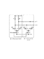
図6は、プリエンファシス機能を備えた出力回路の構成を示す図である(特許文献1参照)。図6を参照すると、出力回路は、ドライバメインバッファ10と、プリエンファシスバッファ20を備えている。ドライバメインバッファ10は、ソースが低位側電源VSSに接続され、ゲートにバイアス電圧BIASを受けるNMOSトランジスタ(電流源トランジスタ)N11と、共通接続されたソースが電流源トランジスタN11のドレインに接続され、ゲートが差動入力端子INT、INBにそれぞれ接続され、ドレインが差動出力端子のOUTB(逆相出力端子あるいは反転出力端子ともいう)、OUTT(正相出力端子あるいは正転出力端子ともいう)にそれぞれ接続されたNMOSトランジスタN1、N2と、差動出力端子OUTB、OUTT(すなわちNMOSトランジスタN1、N2のドレイン)と高位側電源VDD間にそれぞれ接続された抵抗R1、R2と、を備えている。
FIG. 6 is a diagram showing a configuration of an output circuit having a pre-emphasis function (see Patent Document 1). Referring to FIG. 6, the output circuit includes a driver
プリエンファシスバッファ20は、ソースがVSSに接続され、ゲートにバイアス電圧BIASを受けるNMOSトランジスタ(電流源トランジスタ)N12と、共通接続されたソースが電流源トランジスタN12のドレインに接続され、制御信号(エンファシス信号)を差動で入力する端子EMT、EMBにゲートがそれぞれ接続され、ドレインが差動出力端子OUTB、OUTTにそれぞれ接続されたNMOSトランジスタN3、N4と、を備えている。なお、OUTT、OUTB、EMT、EMB等において、端子名、信号名の末尾のTは正相(True)、Bは逆相(Bar)を表す。
The
図7は、図6の回路の動作を説明するタイミングチャートである。図7のタイミングチャートは、図6の回路動作を説明するために、本願発明者により新たに作成されたものである。図7には、図6の端子INT、INB、端子EMT、EMB、端子OUTB、コモンモード電圧(VCM)、端子OUTT、NMOSトランジスタN12のドレインノードVS2、NMOSトランジスタN11のドレインノードVS1の電圧波形と、NMOSトランジスタN1、N2、N3、N4のON(オン)、OFF(オフ)の状態が示されている。図7において、INTの上の(1)〜(11)はタイミング期間を表している。図6の回路動作の詳細を図7のタイミングチャートを参照して説明する。なお、以下では、端子名と該端子の信号名を共通に用いる。 FIG. 7 is a timing chart for explaining the operation of the circuit of FIG. The timing chart of FIG. 7 is newly created by the inventor of the present application in order to explain the circuit operation of FIG. FIG. 7 shows the voltage waveforms of the terminals INT, INB, terminals EMT, EMB, terminal OUTB, common mode voltage (VCM), the terminal OUTT, the drain node VS2 of the NMOS transistor N12, and the drain node VS1 of the NMOS transistor N11 in FIG. , NMOS transistors N1, N2, N3, and N4 are shown in an ON state and an OFF state. In FIG. 7, (1) to (11) above INT represent timing periods. Details of the circuit operation of FIG. 6 will be described with reference to the timing chart of FIG. In the following, the terminal name and the signal name of the terminal are used in common.
<期間(1)>
(INT、INB)は直前の(Low、High)から(High、Low)に遷移し、(EMT、EMB)=(High、Low)とされる。このとき、NMOSトランジスタN1、N3がONし、NMOSトランジスタN2、N4がOFFし、差動出力信号OUTT、OUTBはそれぞれHigh、Low側にプリエンファシスがかかったレベルとなる。このときの出力Lowレベル(VOLP:プリエンファシスのかかったLowレベル出力電圧)は低く、電流源トランジスタN11、N12のドレインノードVS1、VS2の電圧も低くなる。すなわち、出力回路の差動入力端子(INT、INB)に入力される信号(相補信号)が、(Low、High)から(High、Low)に変化する場合に、(EMT、EMB)は(High、Low)に設定され、(OUTT、OUTB)は(VOHP、VOLP)に設定される。
<Period (1)>
(INT, INB) changes from (Low, High) to (High, Low) immediately before, and (EMT, EMB) = (High, Low). At this time, the NMOS transistors N1 and N3 are turned on, the NMOS transistors N2 and N4 are turned off, and the differential output signals OUTT and OUTB are at levels at which pre-emphasis is applied to the High and Low sides, respectively. At this time, the output low level (VOLP: low-level output voltage subjected to pre-emphasis) is low, and the voltages of the drain nodes VS1 and VS2 of the current source transistors N11 and N12 are also low. That is, when the signals (complementary signals) input to the differential input terminals (INT, INB) of the output circuit change from (Low, High) to (High, Low), (EMT, EMB) is (High). , Low) and (OUTT, OUTB) are set to (VOHP, VOLP).
<期間(2)>
(INT、INB)=(High、Low)、(EMT、EMB)=(Low、High)とされる。出力回路の差動入力端子(INT、INB)に入力される信号(相補信号)が(High、Low)のまま変化しない場合に、(EMT、EMB)は(Low、High)に設定される。OUTT、OUTBはそれぞれVOHPよりも低いレベル、VOLPよりも高いレベル、すなわち、デエンファシスレベルに設定される。期間(2)において、NMOSトランジスタN1はONのままであるが、NMOSトランジスタN3がOFFし、NMOSトランジスタN4がONし、(OUTT、OUTB)は、デエンファシスがかかった波形となる。OUTBのLow電位はNMOSトランジスタN3がOFFのため、NMOSトランジスタN1とN3がともにONとされた期間(1)の電圧VOLPよりも高くなる。また、OUTTのHigh電位はNMOSトランジスタN4がONのため、NMOSトランジスタN2とN4がともにOFFとされた期間(1)の電圧VOHPよりも低くなる。すなわち、プリエンファシスバッファ20において、期間(1)では低い出力レベルVOLPを出力しているOUTBに接続されたNMOSトランジスタN3がONしているのに対し、期間(2)では、出力レベルVOHPを出力しているOUTTに接続されたNMOSトランジスタN4がONする。このため、電流源トランジスタN12のドレイン電圧VS2のレベルがVaからVbに上がる。
<Period (2)>
(INT, INB) = (High, Low), (EMT, EMB) = (Low, High). When signals (complementary signals) input to the differential input terminals (INT, INB) of the output circuit remain unchanged (High, Low), (EMT, EMB) is set to (Low, High). OUTT and OUTB are set to a level lower than VOHP and a level higher than VOLP, that is, a de-emphasis level, respectively. In the period (2), the NMOS transistor N1 remains ON, but the NMOS transistor N3 is turned OFF, the NMOS transistor N4 is turned ON, and (OUTT, OUTB) has a waveform subjected to de-emphasis. Since the NMOS transistor N3 is OFF, the low potential of OUTB is higher than the voltage VOLP during the period (1) when both the NMOS transistors N1 and N3 are ON. Further, the High potential of OUTT is lower than the voltage VOHP during the period (1) in which both the NMOS transistors N2 and N4 are OFF because the NMOS transistor N4 is ON. That is, in the
図8は、図6の回路のプリエンファシスバッファの電流源トランジスタN12のドレイン・ソース間電圧Vds(x軸)とドレイン電流Id(y軸)の特性を示している。図8のVds−Id特性から、電流源トランジスタN12のドレインノードVS2の電圧がVaからVbに上がることによって、NMOSトランジスタN12のドレイン電流値IdはIaからIbにdI分増加する。このため、期間(2)におけるコモンモード電圧(VCM)は、期間(1)におけるコモンモード電圧(VCM)よりも低下する。 FIG. 8 shows the characteristics of the drain-source voltage Vds (x axis) and the drain current Id (y axis) of the current source transistor N12 of the pre-emphasis buffer of the circuit of FIG. From the Vds-Id characteristic of FIG. 8, when the voltage of the drain node VS2 of the current source transistor N12 increases from Va to Vb, the drain current value Id of the NMOS transistor N12 increases by dI from Ia to Ib. For this reason, the common mode voltage (VCM) in the period (2) is lower than the common mode voltage (VCM) in the period (1).
<期間(3)>
(INT、INB)=(Low、High)、(EMT、EMB)=(Low、High)とされる。INTがHighからLowに遷移するため、EMBをHighとしてNMOSトランジスタN4をONとし、EMTをLowとしてNMOSトランジスタN3をOFFとしてプリエンファシスが行われる。ただし、(EMT、EMB)の値は期間(2)と同一の値とされる。NMOSトランジスタN2、N4がONし、NMOSトランジスタN1、N3がOFFし、差動出力端子OUTT、OUTBはそれぞれLow、High側にプリエンファシスがかかったレベルVOLP、VOHPとなる。電流源トランジスタN11、N12のドレイン電圧VS1、VS2も低くなる。
<Period (3)>
(INT, INB) = (Low, High), (EMT, EMB) = (Low, High). Since INT transitions from High to Low, pre-emphasis is performed by setting EMB to High and the NMOS transistor N4 to ON, and EMT to Low and the NMOS transistor N3 to OFF. However, the values of (EMT, EMB) are the same as those in the period (2). The NMOS transistors N2 and N4 are turned on, the NMOS transistors N1 and N3 are turned off, and the differential output terminals OUTT and OUTB are at levels VOLP and VOHP, respectively, on which pre-emphasis is applied on the Low and High sides. The drain voltages VS1 and VS2 of the current source transistors N11 and N12 are also lowered.
<期間(4)>
(INT、INB)=(Low、High)、(EMT、EMB)=(High、Low)とされる。期間(4)では、期間(3)の状態から(EMT、EMB)の値が反転し、NMOSトランジスタN4がOFFし、NMOSトランジスタN3がONし、差動出力端子OUTT、OUTBは、デエンファシスがかかったレベルとなる。
<Period (4)>
(INT, INB) = (Low, High), (EMT, EMB) = (High, Low). In the period (4), the values of (EMT, EMB) are inverted from the state of the period (3), the NMOS transistor N4 is turned off, the NMOS transistor N3 is turned on, and the differential output terminals OUTT, OUTB are de-emphasized. It becomes the level that took.
プリエンファシスバッファ20において、期間(3)では、プリエンファシスがかかったLowレベルVOLPを出力しているOUTTに接続されたNMOSトランジスタN4がONしているのに対し、期間(4)では、期間(3)にプリエンファシスがかかったHighレベルVOHDを出力していたOUTBに接続されたNMOSトランジスタN3がONする。このため、電流源トランジスタN12のドレインノードVS2の電圧レベルがVaからVbに上がる。期間(2)と同様の理由で、電流源トランジスタN12のドレイン電流がdI増加し、コモンモード電圧(VCM)は、期間(3)のコモンモード電圧(VCM)よりも低下する。
In the
<期間(5)〜(11)>においても、期間(1)から(4)の繰り返しとなる。 Also in <periods (5) to (11)>, the periods (1) to (4) are repeated.
なお、プリエンファシスを制御する信号EMT、EMBを入力信号INT、INBから生成する論理回路はよく知られており、各種実装がある。例えば、EMTは、INTに入力する現在ビットとその直前のビット(フリップフロップに保持される)に関して、
(現在ビット、直前ビット)=(High、Low)のとき、High、
(現在ビット、直前ビット)=(High、High)のとき、Low、
(現在ビット、直前ビット)=(Low、High)のとき、Low、
(現在ビット、直前ビット)=(Low、Low)のとき、High、
となる。EMBはETMの相補信号である。
A logic circuit that generates signals EMT and EMB for controlling pre-emphasis from input signals INT and INB is well known, and there are various implementations. For example, the EMT has the current bit input to the INT and the bit immediately preceding it (held in the flip-flop).
When (current bit, previous bit) = (High, Low), High,
When (current bit, previous bit) = (High, High), Low,
When (current bit, previous bit) = (Low, High), Low,
When (current bit, previous bit) = (Low, Low), High,
It becomes. EMB is a complementary signal of ETM.
図6に示した出力回路は、VCM変動を抑制する機能を具備していないため、上記したように、トランジション・ビットとデエンファシス・ビット間でコモンモード電圧(VCM)に不一致が生じ、VCMの変動が大きくなる(劣化する)場合がある。すなわち、高電源電圧化、小出力振幅化等の仕様の変更を行わないと、標準インターフェース規格(PCI−Express/Serial−ATA/CEI)を逸脱する可能性がある。図11に示したように、SATA(Serial−Advanced Technology Attachment)では、ACコモンモード電圧変動(Vcmac)仕様は50mVppとされる。 Since the output circuit shown in FIG. 6 does not have a function of suppressing the VCM fluctuation, as described above, a mismatch occurs in the common mode voltage (VCM) between the transition bit and the de-emphasis bit, and the VCM The fluctuation may become large (deteriorate). That is, there is a possibility of deviating from the standard interface standard (PCI-Express / Serial-ATA / CEI) unless specifications are changed such as higher power supply voltage and lower output amplitude. As shown in FIG. 11, in the SATA (Serial-Advanced Technology Attachment), the AC common mode voltage fluctuation (Vcmac) specification is 50 mVpp.
標準インターフェース規格に対応した出力回路は、低消費電力化のために、低電源電圧で動作することが要求される。図6の回路において、低い電源電圧で、PCI−Expressのように大きな差動出力振幅(800mV以上、1200mV以下)を実現しようとしたとき、トランジション・ビットとデエンファシス・ビット間のコモンモード電圧(VCM)の変動が大きくなる。VCMの変動が大となると、差動出力端子OUTT、OUTBからの差動信号を受信する受信回路(差動受信回路)の入力における遅延が変動し、この遅延変動はジッタとなり、受信回路が受信可能な時間区間が減少し、ジッタ耐性が低くなる。 An output circuit corresponding to the standard interface standard is required to operate at a low power supply voltage in order to reduce power consumption. In the circuit of FIG. 6, when a large differential output amplitude (800 mV or more and 1200 mV or less) is achieved with a low power supply voltage as in PCI-Express, the common mode voltage between the transition bit and the de-emphasis bit ( VCM) fluctuates. When the fluctuation of VCM becomes large, the delay at the input of the receiving circuit (differential receiving circuit) that receives the differential signal from the differential output terminals OUTT and OUTB fluctuates, and this delay fluctuation becomes jitter, and the receiving circuit receives it. The possible time interval is reduced and jitter tolerance is reduced.
図9は、帰還回路を用いVCMを安定化させる一般的な回路構成を示す図である。図9を参照すると、ドライバメインバッファ10’、プリエンファシスバッファ20’、VCM帰還部21を備えている。ドライバメインバッファ10’は、図6の構成において、NMOSトランジスタN1、N2のドレインに一端が接続された負荷抵抗素子R1、R2の他端を共通接続し、その共通接続点と高位側電源VDD間に、PMOSトランジスタP1を備えている。VCM帰還部21は、プリエンファシスドライバ20’において、OUTTとOUTBの中点電圧COM(OUTTとOUTB間の抵抗R3とR4の接続点電圧)を非反転入力に入力し、コモンモード基準電圧(VCMREF)を反転入力に入力し、出力をPMOSトランジスタP1のゲートに接続したオペアンプ(OPAMP)を備えている。オペアンプ(OPAMP)は中点電圧(コモンモード電圧)(COM)がVCMREFと一致するように、PMOSトランジスタP1のゲート電圧を制御し、PMOSトランジスタP1のドレイン電圧VD1(負荷抵抗素子R1、R2の接続点の電圧)を調整することで、コモンモード電圧(COM)に帰還がかかる。このVCMの安定化方法では、その追従スピードは、オペアンプ(OPAMP)とPMOSトランジスタP1を含む帰還回路の追従スピードに依存する。このため、図9の回路は、例えば数十MHz程度以下のVCM変動に対しては、有効であるが、PCI−Express/Serial−ATA/CEIなどの標準インターフェースにおける、トランジション・ビットとデエンファシス・ビット間のVCM変動のような、1GHzを超える高速なVCM変動には追従できず、対応不可能である。
FIG. 9 is a diagram showing a general circuit configuration for stabilizing the VCM using a feedback circuit. Referring to FIG. 9, a driver
特許文献1では、そのFig.4に示すように、図6の回路のプリエンファシスバッファのNMOSトランジスタN3、N4のドレインに、ドレインがそれぞれ接続された二つのPMOSトランジスタを備え、これら二つのPMOSトランジスタの共通接続されたソースと電源VDD間に第3のPMOSトランジスタを備え、デエンファシス・ビットのコモンモードの変動を補償している。この場合、トランジスタが縦積み4段となり、低電源電圧には不向きである。またPMOSトランジスタが抵抗R1、R2と並列接続となるため、DCインピーダンスが低下する。
In
図10に、特許文献2に開示されている出力回路(電流モード論理ドライバ)の構成を示す。なお、図10は、特許文献2の図5の構成に基づいて作成したものである。図10において、ドライバメインバッファ10、プリエンファシスバッファ20は、図6の構成と同一である。図10に示すように、高位側電源VDDとOUTT間にVCMプルアップ機構の電流源Ipu、OUTTと低位側電源VSS間にVCMプルダウン機構の電流源Ipdを備え、高位側電源VDDとOUTB間にVCMプルアップ機構の電流源Ipu、OUTBと低位側電源VSS間にVCMプルダウン機構のIpdを備えたレベルシフト機構を備えている。出力回路の差動出力端子OUTT、OUTB間に接続された抵抗R3は、負荷抵抗である。
FIG. 10 shows the configuration of the output circuit (current mode logic driver) disclosed in
以下では、考察を簡単にするため、プリエンファシスバッファ20が動作していない状態(したがってNMOSトランジスタN3とNMOSトランジスタN4はともにOFF)であるものとする。NMOSトランジスタN1がON、NMOSトランジスタN2がOFFしているものとする。回路の電流経路はI1とI2の2系統あり、電流値は抵抗素子R1、R2、R3の比によって決定される。このとき、出力端子OUTTは、Highレベル(VOH)を出力しており、そのレベルは、
VOH=VDD−I2×R2
である。
In the following, in order to simplify the discussion, it is assumed that the
VOH = VDD−I2 × R2
It is.
一方、出力端子OUTBはLowレベル(VOL)を出力しており、
VOL=VDD−I1×R1
である。
On the other hand, the output terminal OUTB outputs a low level (VOL),
VOL = VDD−I1 × R1
It is.
コモンモード電圧(VCM)は、
VCM=(VOH+VOL)/2
=VDD−(I1×R1+I2×R2)/2
で表される。
The common mode voltage (VCM) is
VCM = (VOH + VOL) / 2
= VDD- (I1 * R1 + I2 * R2) / 2
It is represented by
コモンモード電圧(VCM)を上昇させたいときには、差動出力端子(OUTT、OUTB)と電源VDD間に接続されたVCMプルアップ機構の二つの定電流源IpuをともにONさせ、差動出力端子(OUTT、OUTB)とGND(VSS)間に接続されたVCMプルダウン機構の二つの定電流源IpdをOFFさせる。 When it is desired to increase the common mode voltage (VCM), the two constant current sources Ipu of the VCM pull-up mechanism connected between the differential output terminals (OUTT, OUTB) and the power supply VDD are both turned on, and the differential output terminal ( The two constant current sources Ipd of the VCM pull-down mechanism connected between OUTT, OUTB) and GND (VSS) are turned off.
このとき、出力Highレベルは、
VOH=VDD−(I2−Ipu)×R2、
出力Lowレベルは、
VOL=VDD−(I1−Ipu)×R1
である。
At this time, the output high level is
VOH = VDD− (I2−Ipu) × R2,
The output low level is
VOL = VDD- (I1-Ipu) * R1
It is.
コモンモード電圧(VCM)は、
VCM=(VOH+VOL)/2
=VDD−(I1×R1+I2×R2)/2+Ipu×(R1+R2)/2
であり、Ipu×(R1+R2)/2分、VCMの電位が上昇する。
The common mode voltage (VCM) is
VCM = (VOH + VOL) / 2
= VDD- (I1 * R1 + I2 * R2) / 2 + Ipu * (R1 + R2) / 2
And the potential of the VCM increases by Ipu × (R1 + R2) / 2 minutes.
コモンモード電圧(VCM)を低下させたいときには、差動出力端子(OUTT、OUTB)と電源(VDD)間に接続されたVCMプルアップ機構の二つの定電流源IpuをOFFさせ、差動出力端子(OUTT、OUTB)とGND(VSS)間に接続されたVCMプルダウン機構の二つの定電流源IpdをONさせる。このとき、出力Highレベルは、
VOH=VDD−(I2+Ipd)×R2、
出力Lowレベルは、
VOL=VDD−(I1+Ipd)×R1
である。
When it is desired to lower the common mode voltage (VCM), the two constant current sources Ipu of the VCM pull-up mechanism connected between the differential output terminals (OUTT, OUTB) and the power supply (VDD) are turned off, and the differential output terminal Two constant current sources Ipd of the VCM pull-down mechanism connected between (OUTT, OUTB) and GND (VSS) are turned ON. At this time, the output high level is
VOH = VDD− (I2 + Ipd) × R2,
The output low level is
VOL = VDD− (I1 + Ipd) × R1
It is.
コモンモード電圧(VCM)は、
VCM=(VOH+VOL)/2
=VDD−(I1×R1+I1×R2)/2−Ipd×(R1+R2)/2
であり、Ipd×(R1+R2)/2分、VCMの電位は低下する。
The common mode voltage (VCM) is
VCM = (VOH + VOL) / 2
= VDD- (I1 * R1 + I1 * R2) / 2-Ipd * (R1 + R2) / 2
And the potential of the VCM decreases by Ipd × (R1 + R2) / 2 minutes.
このように、出力端子(OUTT、OUTB)と電源(VDD)間に接続されたVCMプルアップ機構の定電流源Ipuと出力端子(OUTT、OUTB)とGND(VSS)間に接続されたVCMプルダウン機構の定電流源Ipdの電流値を制御することで、VCMを調整できる。 Thus, the VCM pull-down connected between the constant current source Ipu of the VCM pull-up mechanism connected between the output terminals (OUTT, OUTB) and the power supply (VDD), and between the output terminals (OUTT, OUTB) and GND (VSS). The VCM can be adjusted by controlling the current value of the constant current source Ipd of the mechanism.
以下に本発明による関連技術の分析を与える。 The following is an analysis of the related art according to the present invention.
図10に示した回路においては、プリエンファシスがかかったトランジション・ビットの出力波形とデエンファシス・ビットの出力波形の両方のコモンモード電圧(VCM)を調整するものである。また図10に示した出力回路においては、差動出力OUTT/OUTBにそれぞれVCMプルアップ機構の二つの定電流源Ipuを構成するPMOSトランジスタと、VCMプルダウン機構の定電流源トランジスタが接続されている。低消費電力化を実現するために、電源電圧VDDが低くなった場合、図10の構成のように、コモンモード電圧(VCM)を単純に引き上げるだけでは、限界が生じ、トランジション・ビットとデエンファシス・ビット間のコモンモード電圧(VCM)のずれは解消されない。このため、デエンファシス・ビット時にだけ、コモンモード電圧(VCM)を調整できる機能が必要となる(本発明者による分析結果)。 In the circuit shown in FIG. 10, the common mode voltage (VCM) of both the output waveform of the transition bit subjected to pre-emphasis and the output waveform of the de-emphasis bit is adjusted. In the output circuit shown in FIG. 10, a PMOS transistor constituting two constant current sources Ipu of the VCM pull-up mechanism and a constant current source transistor of the VCM pull-down mechanism are connected to the differential outputs OUTT / OUTB, respectively. . When the power supply voltage VDD is lowered to achieve low power consumption, simply raising the common mode voltage (VCM) as shown in the configuration of FIG. 10 causes a limit, and the transition bit and de-emphasis・ Difference in common mode voltage (VCM) between bits cannot be resolved. Therefore, a function capable of adjusting the common mode voltage (VCM) is required only at the time of de-emphasis bit (analysis result by the present inventor).
定電流源トランジスタは、理想的には出力インピーダンスは無限大であるが、実際にはインピーダンスは低くなり、さらに電源電圧が低くなると、高いインピーダンスを保つのは困難である。図10の回路において、出力端子OUTT、OUTBに接続された定電流源の出力インピーダンスが低くなると、出力回路のインピーダンスが低くなり、標準インターフェース規格(PCI−Express/Serial−ATA/CEI)を逸脱する可能性がある。 The constant current source transistor ideally has an infinite output impedance. However, in practice, the impedance is low, and when the power supply voltage is low, it is difficult to maintain a high impedance. In the circuit of FIG. 10, when the output impedance of the constant current source connected to the output terminals OUTT and OUTB becomes low, the impedance of the output circuit becomes low and deviates from the standard interface standard (PCI-Express / Serial-ATA / CEI). there is a possibility.
また、図10の回路においては、出力端子OUTT、OUTBにそれぞれ定電流源を接続しており、出力端子OUTT、OUTBに大きな拡散層容量が付くことによって、高速動作への対応ができなくなる。 In the circuit of FIG. 10, constant current sources are connected to the output terminals OUTT and OUTB, respectively, and a large diffusion layer capacitance is added to the output terminals OUTT and OUTB, so that it is impossible to cope with high-speed operation.
前記問題の1つ又は複数を解消するため、本発明は概略以下の構成とされる。 In order to solve one or more of the above problems, the present invention is roughly configured as follows.
本発明によれば、入力信号を差動入力して差動出力し、前記入力信号の遷移時に差動出力信号にプリエンファシスをかける出力回路であって、プリエンファシス時には、前記差動出力信号のプリエンファシス作用を補強し、デエンファシス時には、前記差動出力信号のプリエンファシスを行っていたパスをオフし、高位側電源と低位側電源間の電流パスをオンする回路を備えている。 According to the present invention, there is provided an output circuit that differentially inputs and outputs an input signal and applies pre-emphasis to the differential output signal at the time of transition of the input signal. A pre-emphasis function is reinforced, and a circuit that turns off the path that pre-emphasized the differential output signal and turns on the current path between the high-order power supply and the low-order power supply during de-emphasis.
本発明によれば、第1の電流源で駆動され、入力信号を差動入力し、出力対が差動出力端子に接続された第1の差動トランジスタ対と、
第2の電流源で駆動され、第1の制御信号を差動入力し、出力対が前記差動出力端子に接続された第2の差動トランジスタ対と、
を備え、前記差動出力端子と電源間に負荷抵抗素子対が接続され、
第3の電流源で駆動され、第2の制御信号を差動入力し、出力対が前記差動出力端子の一方の出力端子と前記電源とに接続された第3の差動トランジスタ対と、
第4の電流源で駆動され、第3の制御信号を差動入力し、出力対が前記電源と前記差動出力端子の他方の出力端子とに接続された第4の差動トランジスタ対と、
を備えている出力回路が提供される。本発明によれば、上記出力回路を備えた半導体装置が提供される。
According to the present invention, a first differential transistor pair driven by a first current source, differentially input an input signal, and an output pair connected to a differential output terminal;
A second differential transistor pair driven by a second current source, differentially inputted with a first control signal, and having an output pair connected to the differential output terminal;
A load resistance element pair is connected between the differential output terminal and the power source,
A third differential transistor pair driven by a third current source, differentially inputted with a second control signal, and an output pair connected to one output terminal of the differential output terminal and the power source;
A fourth differential transistor pair driven by a fourth current source, differentially input a third control signal, and an output pair connected to the power source and the other output terminal of the differential output terminal;
An output circuit is provided. According to the present invention, a semiconductor device including the output circuit is provided.
本発明によれば、プリエンファシス時とデエンファシス時の差動出力信号のコモンモード電圧の変化を抑えることができる。また、本発明によれば、高速なコモンモード電圧変動に追従することができる。 According to the present invention, it is possible to suppress a change in the common mode voltage of the differential output signal during pre-emphasis and de-emphasis. Further, according to the present invention, it is possible to follow high-speed common mode voltage fluctuations.
本発明の実施形態について以下に説明する。本発明は、一態様(モード)において、第1の電流源(N11)で駆動され、入力信号(INT、INB)を差動入力し、出力対が差動出力端子(OUTB、OUTT)に接続された第1の差動トランジスタ対(N1、N2)と、第2の電流源(N12)で駆動され、第1の制御信号(EMT、EMB)を差動入力し、出力対が前記差動出力端子(OUTB、OUTT)に接続された第2の差動トランジスタ対(N3、N4)と、を備え、前記差動出力端子(OUTB、OUTT)と電源(VDD)間に負荷抵抗素子対(R1、R2)が接続されている。本発明においては、さらに、デエンファシスレベル制御バッファ(30)を備えている。デエンファシスレベル制御バッファ(30)は、第3の電流源(N13)で駆動され、第2の制御信号(DET、OFT)を差動入力し、出力対が前記差動出力端子の一方の出力端子(OUTT)と前記電源(VDD)とに接続された第3の差動トランジスタ対(N5、N6)と、第4の電流源(N14)で駆動され、第3の制御信号(OFB、DEB)を差動入力し、出力対が前記電源(VDD)と前記差動出力端子の他方の出力端子(OUTB)とに接続された第4の差動トランジスタ対(N7、N8)とを備えている。 Embodiments of the present invention will be described below. In one aspect (mode), the present invention is driven by the first current source (N11), differentially inputs the input signals (INT, INB), and the output pair is connected to the differential output terminals (OUTB, OUTT). Driven by the first differential transistor pair (N1, N2) and the second current source (N12), the first control signal (EMT, EMB) is differentially input, and the output pair is the differential A second differential transistor pair (N3, N4) connected to the output terminals (OUTB, OUTT), and a load resistive element pair (between the differential output terminals (OUTB, OUTT) and the power source (VDD)). R1, R2) are connected. The present invention further includes a de-emphasis level control buffer (30). The de-emphasis level control buffer (30) is driven by the third current source (N13), differentially inputs the second control signals (DET, OFT), and the output pair is one output of the differential output terminal. The third differential transistor pair (N5, N6) connected to the terminal (OUTT) and the power source (VDD) and the fourth current source (N14) are driven, and the third control signal (OFB, DEB). ) And a fourth differential transistor pair (N7, N8) connected to the power supply (VDD) and the other output terminal (OUTB) of the differential output terminal. Yes.
本発明においては、自集積回路(半導体装置)の信号を他集積回路(半導体装置)へ伝送路を介して送信するための差動出力回路において、デエンファシス時における差動出力信号のコモンモード電圧(VCM)の変化を補償し、コモンモード電圧(VCM)の変動の劣化を改善している。また、低電源電圧で出力回路を構成した場合、大振幅出力時に、High出力時とLow出力時のプリエンファシス波形に不均衡、すなわちプリエンファシスがかかったトランジション・ビットとプリエンファシスがかかっていないデエンファシス・ビット間のコモンモード電圧(VCM)変動を改善・調整する。以下、実施例に即して説明する。 In the present invention, in a differential output circuit for transmitting a signal of its own integrated circuit (semiconductor device) to another integrated circuit (semiconductor device) via a transmission line, the common mode voltage of the differential output signal at the time of de-emphasis (VCM) change is compensated for, and deterioration of common mode voltage (VCM) fluctuation is improved. Also, when the output circuit is configured with a low power supply voltage, the pre-emphasis waveform at high output and low output is unbalanced at the time of large amplitude output, that is, the pre-emphasis transition bit and the pre-emphasis are not applied. Improve and adjust common mode voltage (VCM) fluctuation between emphasis bits. In the following, description will be made in accordance with examples.
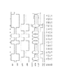
図1は、本発明の一実施例の構成を示す図である。図1を参照すると、この出力回路は、ドライバメインバッファ10と、プリエンファシスバッファ20と、デエンファシスレベル制御バッファ30と、を備えている。ドライバメインバッファ10は、ソースが低位側電源VSSに接続され、ゲートにバイアス電圧BIASを受けるNMOSトランジスタ(電流源トランジスタ)N11と、共通接続されたソースが電流源トランジスタN11のドレインに接続され、ゲートが差動入力端子INT、INBにそれぞれ接続され、ドレインが差動出力端子OUTB、OUTTにそれぞれ接続されたNMOSトランジスタN1、N2(第1の差動トランジスタ対)と、NMOSトランジスタN1、N2のドレインと高位側電源VDD間に接続された負荷抵抗素子R1、R2とを備えている。プリエンファシスバッファ20は、ソースが低位側電源VSSに接続され、ゲートにバイアス電圧BIASを受けるNMOSトランジスタ(電流源トランジスタ)N12と、共通接続されたソースが電流源トランジスタN12のドレインに接続され、ゲートが端子EMT、EMBにそれぞれ接続され、ドレインが差動出力端子OUTB、OUTTにそれぞれ接続されたNMOSトランジスタN3、N4(第2の差動トランジスタ対)と、を備えている。
FIG. 1 is a diagram showing the configuration of an embodiment of the present invention. Referring to FIG. 1, the output circuit includes a driver
デエンファシスレベル制御バッファ30は、ソースが低位側電源VSSに接続され、ゲートにバイアス電圧BIASを受けるNMOSトランジスタ(電流源トランジスタ)N13と、共通接続されたソースが電流源トランジスタN13のドレインに接続され、ゲートが端子DET、OFTにそれぞれ接続され、ドレインがOUTTと電源VDDにそれぞれ接続されたNMOSトランジスタN5、N6(第3の差動トランジスタ対)と、ソースがVSSに接続され、ゲートにバイアス電圧BIASを受けるNMOSトランジスタ(電流源トランジスタ)N14と、共通接続されたソースが電流源トランジスタN14のドレインに接続され、ゲートが端子OFB、DEBにそれぞれ接続され、ドレインが電源VDDとOUTBにそれぞれ接続されたNMOSトランジスタN7、N8(第4の差動トランジスタ対)とを備えている。第3の差動トランジスタ対(N5、N6)のゲートに接続する端子DET、OFTには相補の制御信号が入力され、第4の差動トランジスタ対(N7、N8)のゲートに接続する端子OFB、DEBには相補の制御信号が入力される。
The de-emphasis
前述した関連技術の回路においては、低電源電圧構成の出力回路で大振幅を出力するとき、出力Lowレベルの低下に伴い、電流源トランジスタ(図6のN11、N12)のドレインノード(VS1、VS2)の電圧が低下する。このとき、図7のように、プリエンファシスバッファ(図6の20)の定電流源トランジスタN12のドレインノードVS2において、トランジション・ビット(例えば期間(1))よりもデエンファシス・ビット(例えば期間(2)で大きく上昇する。プリエンファシスバッファ(図6の20)の定電流源トランジスタN12のドレインノードVS2における、デエンファシス時とプリエンファシス時の電圧差(Vb−Va)によって、プリエンファシスバッファ(図6の20)の電流源トランジスタN12の電流値は、図8のVds−Id特性からわかるように、差電流(dI)分、上昇する。デエンファシス・ビットにおいて、電流源トランジスタN12のドレイン電流がdI増加することで、デエンファシス時のコモンモード電圧(VCM)は、プリエンファシス時のトランジション・ビットのコモンモードVCMよりも低下し、コモンモード電圧(VCM)の変動を劣化させる。 In the circuit of the related art described above, when a large amplitude is output by the output circuit having a low power supply voltage configuration, the drain nodes (VS1, VS2) of the current source transistors (N11, N12 in FIG. 6) are accompanied with a decrease in the output Low level. ) Voltage decreases. At this time, as shown in FIG. 7, in the drain node VS2 of the constant current source transistor N12 of the pre-emphasis buffer (20 in FIG. 6), the de-emphasis bit (for example, the period (1)) rather than the transition bit (for example, the period (1)). 2), the pre-emphasis buffer (FIG. 6) depends on the voltage difference (Vb−Va) between the de-emphasis and the pre-emphasis at the drain node VS2 of the constant current source transistor N12 of the pre-emphasis buffer (20 in FIG. 6). 6), the current value of the current source transistor N12 rises by the difference current (dI) as can be seen from the Vds-Id characteristic of Fig. 8. In the de-emphasis bit, the drain current of the current source transistor N12 is By increasing dI, the common mode voltage during de-emphasis ( CM) is lower than the common mode VCM Transition bit when pre-emphasis, degrade the variation in the common mode voltage (VCM).
これに対して、本実施例においては、図1に示すように、2組の差動トランジスタ対(N5、N6)、(N7、N8)を備えたデエンファシスレベル制御バッファ30において、デエンファシス・ビット時のみ、電流値を小さくすることで、コモンモード電圧(VCM)を上昇させる。これにより、デエンファシス時のコモンモード電圧(VCM)は、プリエンファシス時のトランジション・ビットのコモンモードVCMよりも大幅に低下することを抑制することができる。
On the other hand, in this embodiment, as shown in FIG. 1, in the de-emphasis
デエンファシス・ビット時に電流値を縮減するための信号(DET、DEB、OFT、OFB)は、図3に示した回路によって、信号(INPT、INPB、EMPT、EMPB)から作られる。INPT、INPB、EMPT、EMPBから、それぞれ、インバータ(INV)2段(正転バッファ)を介して、INT、INB、EMT、EMBが出力される。DETは、INPBとEMPBとを受ける2入力NAND回路の出力をインバータで反転した信号であり、OFTは、該NAND回路の出力であり、DETとOFTは相補信号である。DEBは、INPTとEMPTとを受ける2入力NAND回路の出力をインバータで反転した信号であり、OFBは該NAND回路の出力であり、DEBとOFBは相補信号である。 Signals (DET, DEB, OFT, OFB) for reducing the current value during the de-emphasis bit are generated from the signals (INPT, INPB, EMPT, EMPB) by the circuit shown in FIG. INT, INB, EMT, and EMB are output from INPT, INPB, EMPT, and EMPB, respectively, via two stages of inverters (INV) (forward rotation buffers). DET is a signal obtained by inverting the output of a two-input NAND circuit that receives INPB and EMPB by an inverter, OFT is an output of the NAND circuit, and DET and OFT are complementary signals. DEB is a signal obtained by inverting the output of a two-input NAND circuit receiving INPT and EMPT by an inverter, OFB is an output of the NAND circuit, and DEB and OFB are complementary signals.
図4に示すように、(INPB、EMPB)が(High、High)のときだけ、OFTはLow、DETはHighとなり、(INPB、EMPB)が(High、High)以外の値のとき、OFTはHigh、DETはLowである。すなわち、(INT、INB)が(High、Low)から(Low、High)へ遷移するプリエンファシス時(EMB=High)に、OFTがLow、DETがHighとなり、図1のNMOSトランジスタN5をONさせ、それ以外の場合、NMOSトランジスタN5はOFF、NMOSトランジスタN6はONとされる。 As shown in FIG. 4, only when (INPB, EMPB) is (High, High), OFT is Low, DET is High, and when (INPB, EMPB) is a value other than (High, High), OFT is High and DET are Low. That is, at the time of pre-emphasis (EMB = High) in which (INT, INB) transitions from (High, Low) to (Low, High), OFT is Low and DET is High, and the NMOS transistor N5 in FIG. 1 is turned on. In other cases, the NMOS transistor N5 is turned off and the NMOS transistor N6 is turned on.
また、(INPT、EMPT)が(High、High)のときだけ、OFBはLow、DEBはHigh、(INPT、EMPT)が(High、High)以外の値のとき、OFBはHigh、DEBはLowである。すなわち、(INT、INB)が(Low、High)から(High、Low)へ遷移するプリエンファシス時(EMT=High)に、OFBがLow、DEBがHighとなり、図1のNMOSトランジスタN8をONさせ、それ以外の場合、NMOSトランジスタN8をOFF、NMOSトランジスタN7をONさせる。 Only when (INPT, EMPT) is (High, High), OFB is Low, DEB is High, and (INPT, EMPT) is a value other than (High, High), OFB is High, DEB is Low. is there. That is, at the time of pre-emphasis (EMT = High) in which (INT, INB) transitions from (Low, High) to (High, Low), OFB is Low, DEB is High, and the NMOS transistor N8 in FIG. 1 is turned on. In other cases, the NMOS transistor N8 is turned off and the NMOS transistor N7 is turned on.
デエンファシスレベル制御バッファ30における電流源トランジスタN13、N14のW(ゲート幅)サイズを変えることにより、デエンファシス・ビットのコモンモード電圧(VCM)レベルを調整することが可能となる。例えば電流源トランジスタN13、N14のサイズを大きくすることとで、バイアス電圧BIASに対して、出力電流が大となる。
The common mode voltage (VCM) level of the de-emphasis bit can be adjusted by changing the W (gate width) size of the current source transistors N13 and N14 in the de-emphasis
図2は、図1、図3、図4を参照して説明した本実施例の全体の動作を説明するためのタイミングチャートである。図2には、端子INT、INB、EMT、EMB、DET、OFT、OFB、DEB、OUTB、VCM(コモンモード電圧)、端子OUTTの電圧波形と、NMOSトランジスタN1乃至N8のON、OFFの状態が示されている。また、図2において、INTの上の(1)〜(11)はタイミング期間を表している。 FIG. 2 is a timing chart for explaining the overall operation of the present embodiment described with reference to FIGS. 1, 3, and 4. FIG. 2 shows the voltage waveforms of the terminals INT, INB, EMT, EMB, DET, OFT, OFB, DEB, OUTB, VCM (common mode voltage), the terminal OUTT, and the ON / OFF states of the NMOS transistors N1 to N8. It is shown. In FIG. 2, (1) to (11) above INT represent timing periods.
前述したように、OFTは、(INB、EMB)が(High、High)のときだけLow(OFTの相補信号DEBはHigh)となる。OFBは(INT、EMT)が(High、High)のときだけ、Low(OFBの相補信号DEBはHigh)となる。 As described above, OFT is Low (the complementary signal DEB of OFT is High) only when (INB, EMB) is (High, High). OFB is Low (OFB complementary signal DEB is High) only when (INT, EMT) is (High, High).
<期間(1)>
(INT、INB)は(Low、High)から(High、Low)に遷移し、(EMT、EMB)=(High、Low)、(DET、OFT、OFB、DEB)=(Low、High、Low、High)とされる。このとき、NMOSトランジスタN1、N3がONし、NMOSトランジスタN2、N4はOFFし、差動出力OUTT、OUTBはプリエンファシスがかかった波形となる。OUTTはHigh(VDD)、OUTBはLow(VSS)となる。このとき、プリエンファシス作用を強め合うように、NMOSトランジスタN8がONし、NMOSトランジスタN5がOFFしている。NMOSトランジスタN6はON、NMOSトランジスタN7はOFFである。
<Period (1)>
(INT, INB) transitions from (Low, High) to (High, Low), (EMT, EMB) = (High, Low), (DET, OFT, OFB, DEB) = (Low, High, Low, High). At this time, the NMOS transistors N1 and N3 are turned on, the NMOS transistors N2 and N4 are turned off, and the differential outputs OUTT and OUTB have waveforms with pre-emphasis applied. OUTT is High (VDD) and OUTB is Low (VSS). At this time, the NMOS transistor N8 is turned on and the NMOS transistor N5 is turned off so as to strengthen the pre-emphasis action. The NMOS transistor N6 is ON and the NMOS transistor N7 is OFF.
<期間(2)>
(INT、INB)=(High、Low)、(EMT、EMB)=(Low、High)、(DET、OFT、OFB、DEB)=(Low、High、High、Low)とされる。このとき、NMOSトランジスタN1はON状態を保ち、プリエンファシスを弱めるようにNMOSトランジスタN3がOFFする。NMOSトランジスタN2はOFF状態を保ち、NMOSトランジスタN4がONし、差動出力OUTT、OUTBはデエンファシスがかかった波形となる。NMOSトランジスタN5とNMOSトランジスタN8はともにOFFし、NMOSトランジスタN6とNMOSトランジスタN7のドレインは、差動出力OUTT、OUTBではなく、電源VDDに接続されており、OFTがHigh、OFBがHighのため、ともにONすることで、電源側に電流を流し、デエンファシス時の回路側に流れる電流値を小さくし、コモンモード電圧(VCM)の低下を抑制している。
<Period (2)>
(INT, INB) = (High, Low), (EMT, EMB) = (Low, High), (DET, OFT, OFB, DEB) = (Low, High, High, Low). At this time, the NMOS transistor N1 is kept on, and the NMOS transistor N3 is turned off to weaken pre-emphasis. The NMOS transistor N2 is kept in the OFF state, the NMOS transistor N4 is turned on, and the differential outputs OUTT and OUTB have a waveform subjected to de-emphasis. Both the NMOS transistor N5 and the NMOS transistor N8 are turned off, and the drains of the NMOS transistor N6 and the NMOS transistor N7 are connected to the power supply VDD instead of the differential outputs OUTT and OUTB, because OFT is High and OFB is High. When both are turned ON, a current flows to the power supply side, a current value flowing to the circuit side during de-emphasis is reduced, and a decrease in common mode voltage (VCM) is suppressed.
<期間(3)>
(INT、INB)=(Low、High)、(EMT、EMB)=(Low、High)、(DET、OFT、OFB、DEB)=(High、Low、High、Low)とされる。NMOSトランジスタN2がONし、NMOSトランジスタN4がONし、NMOSトランジスタN1がOFF、NMOSトランジスタN3がOFFし、差動出力OUTT、OUTBはプリエンファシスがかかった波形となる。このとき、プリエンファシス作用を強め合うようにNMOSトランジスタN5がONし、NMOSトランジスタN8はOFFしている。NMOSトランジスタN6はOFF、NMOSトランジスタN7はONしている。
<Period (3)>
(INT, INB) = (Low, High), (EMT, EMB) = (Low, High), (DET, OFT, OFB, DEB) = (High, Low, High, Low). The NMOS transistor N2 is turned on, the NMOS transistor N4 is turned on, the NMOS transistor N1 is turned off, the NMOS transistor N3 is turned off, and the differential outputs OUTT and OUTB have waveforms with pre-emphasis applied. At this time, the NMOS transistor N5 is turned on and the NMOS transistor N8 is turned off so as to strengthen the pre-emphasis action. The NMOS transistor N6 is OFF and the NMOS transistor N7 is ON.
<期間(4)>
(INT、INB)=(Low、High)、(EMT、EMB)=(High、Low)、(DET、OFT、OFB、DEB)=(Low、High、High、Low)とされる。NMOSトランジスタN2はONを保ち、プリエンファシスを弱めるようにNMOSトランジスタN4がOFFする。NMOSトランジスタN1はOFF状態を保ち、NMOSトランジスタN3がONし、差動出力OUTT/OUTBはデエンファシスがかかった波形となる。このとき、NMOSトランジスタN5とNMOSトランジスタN8はともにOFFし、NMOSトランジスタN6とNMOSトランジスタN7はドレインがともに電源VDDに接続されており、OFT、OFBがHighのため、ともにONすることで、電源側に電流を流し、デエンファシス時の回路側に流れる電流値を小さくし、VCMの低下を抑制している。
<Period (4)>
(INT, INB) = (Low, High), (EMT, EMB) = (High, Low), (DET, OFT, OFB, DEB) = (Low, High, High, Low). The NMOS transistor N2 is kept on, and the NMOS transistor N4 is turned off to weaken pre-emphasis. The NMOS transistor N1 is kept OFF, the NMOS transistor N3 is turned ON, and the differential output OUTT / OUTB has a waveform with de-emphasis applied. At this time, both the NMOS transistor N5 and the NMOS transistor N8 are turned off, and the drains of the NMOS transistor N6 and the NMOS transistor N7 are both connected to the power supply VDD, and since both OFT and OFB are High, the both are turned on. The current value flowing in the circuit side at the time of de-emphasis is reduced to suppress the decrease in VCM.
<期間(5)〜(11)>
上記(1)乃至(4)の繰り返しとなる。
<Period (5) to (11)>
The above (1) to (4) are repeated.
ここで、仮に、差動対を構成するNMOSトランジスタN5、N6と、差動対を構成するNMOSトランジスタN7、N8を配設するかわりに、NMOSトランジスタN5とN8のソースを共通接続して電流源トランジスタN13のドレインに接続し、NMOSトランジスタN6、N7を削除した場合、デエンファシス時にNMOSトランジスタN5とN8のゲート電圧がともにLowとなりともにオフ状態となる場合が生じる。この場合、図6、図7を参照して説明した関連技術の問題点であるコモンモード電圧(VCM)のずれを解消することはできない。 Here, instead of providing the NMOS transistors N5 and N6 constituting the differential pair and the NMOS transistors N7 and N8 constituting the differential pair, the sources of the NMOS transistors N5 and N8 are connected in common to each other. If the NMOS transistors N6 and N7 are deleted by connecting to the drain of the transistor N13, the gate voltages of the NMOS transistors N5 and N8 are both low during the de-emphasis, and may be turned off. In this case, the common mode voltage (VCM) shift, which is a problem of the related art described with reference to FIGS. 6 and 7, cannot be eliminated.
本実施例によれば、デエンファシス時のコモンモード電圧(VCM)のレベルを、トランジション・ビット時のVCMと同等となるように最適化することで、VCM変動を低減し、標準インターフェース規格(PCI−Express/Serial−ATA/CEI)のVCMの変動仕様に対応できる。 According to this embodiment, by optimizing the level of the common mode voltage (VCM) at the time of de-emphasis so as to be equivalent to the VCM at the time of transition bit, the VCM fluctuation is reduced and the standard interface standard (PCI -Express / Serial-ATA / CEI) VCM variation specifications can be supported.
本実施例によれば、デエンファシス時のコモンモード電圧(VCM)レベルを外部から調整可能としておくことで、設計と実機でVCM変動に差が生じた場合でも、再設計することなく改善が可能である。 According to the present embodiment, the common mode voltage (VCM) level at the time of de-emphasis can be adjusted from the outside, so that even if there is a difference in the VCM fluctuation between the design and the actual machine, it can be improved without redesign. It is.
高速標準インターフェース(PCI−Express/Serial−ATA/CEI)のトランジション・ビットとデエンファシス・ビット間の高速なVCM変動に追従するためには、出力回路の出力データと同じスピードでコモンモード電圧(VCM)変動を抑制できる必要がある。 In order to follow the high-speed VCM fluctuation between the transition bit and de-emphasis bit of the high-speed standard interface (PCI-Express / Serial-ATA / CEI), the common mode voltage (VCM) at the same speed as the output data of the output circuit. ) It must be possible to suppress fluctuations.
図5は、本実施例によるシミュレーション結果を示す図である。プリエンファシス時のトランジション・ビットとデエンファシス・ビット間でコモンモード電圧(VCM)の変動が抑制されていることがわかる。また、図1の電流源トランジスタN13、N14の電流値を増加させると、デエンファシス・ビットのコモンモード電圧(VCM)が上昇していることがわかる。電流源トランジスタN13、N14は、電流源トランジスタN11、N12と同一のバイアス電圧BIASを受ける構成とされており、この構成で、電流源トランジスタN13、N14の電流値を増加させる場合、例えば電流源トランジスタN13、N14のサイズ(W/L:ゲート幅/ゲート長)を大きく設定することで対処する。 FIG. 5 is a diagram showing a simulation result according to the present embodiment. It can be seen that the variation of the common mode voltage (VCM) is suppressed between the transition bit and the de-emphasis bit during pre-emphasis. Further, it can be seen that when the current values of the current source transistors N13 and N14 in FIG. 1 are increased, the common mode voltage (VCM) of the de-emphasis bit is increased. The current source transistors N13 and N14 are configured to receive the same bias voltage BIAS as the current source transistors N11 and N12. In this configuration, when increasing the current value of the current source transistors N13 and N14, for example, the current source transistors This is dealt with by increasing the size of N13 and N14 (W / L: gate width / gate length).
本実施例においては、例えば図9に示した追従スピードが遅い帰還回路(OPAMPを含む)でVCMを安定化させる構成とは異なり、出力ビットデータの伝送スピードと同じスピードで動作可能な2組の差動対(N5、N6)、(N7、N8)を追加する構成としており、高速なVCM変動に追従することができる。 In this embodiment, for example, unlike the configuration in which the VCM is stabilized by a feedback circuit (including OPAMP) having a slow follow-up speed shown in FIG. 9, two sets that can operate at the same speed as the transmission speed of the output bit data. A differential pair (N5, N6), (N7, N8) is added, and high-speed VCM fluctuation can be followed.
また2組の差動対(N5、N6)、(N7、N8)は、前段論理回路(図3参照)による制御によって、デエンファシス・ビット時にのみ、電流を低減するように動作し、トランジション・ビットと同等のVCMとなるように最適化することで、VCM変動値を低減することが可能である。なお、かかる効果は、例えば、低電源電圧で大振幅のプリエンファシス波形を出力させた場合のように、トランジション・ビットとデエンファシス・ビット間でコモンモード電圧(VCM)が変動する出力回路に特に有効である。 The two differential pairs (N5, N6) and (N7, N8) operate so as to reduce the current only at the time of the de-emphasis bit under the control of the preceding logic circuit (see FIG. 3). It is possible to reduce the VCM fluctuation value by optimizing the VCM to be equivalent to the bit. This effect is particularly effective in an output circuit in which the common mode voltage (VCM) varies between the transition bit and the de-emphasis bit, for example, when a large-amplitude pre-emphasis waveform is output with a low power supply voltage. It is valid.
なお、図1に示した例では、差動対(N1、N2)、(N3、N4)、(N5、N6)、(N7、N8)をNMOSトランジスタで構成した例について説明したが、極性をかえてPMOSトランジスタで構成してもよいことは勿論である。この場合、定電流源トランジスタN11、N12、N13、N14はPMOSトランジスタで構成される。また負荷抵抗R1、R2は能動素子で構成してもよいことは勿論である。本発明は、高速シリアル伝送を行うSerDes(シリアライザ/デシリアライザ)インタフェース等のシリアライザ側の出力ドライバ回路等、半導体装置間の差動伝送を行う出力回路に適用して好適とされる。
なお、上記した実施形態は以下のように付記される(ただし、以下に限定されない)。
(形態1)
入力信号を差動入力して差動出力し、前記入力信号の遷移時に差動出力信号にプリエンファシスをかける出力回路であって、
プリエンファシス時には、前記差動出力信号のプリエンファシス作用を補い、
デエンファシス時には、前記プリエンファシス時に前記差動出力信号のプリエンファシスを行っていたパスをオフし、電源間の電流パスをオンする差動回路を備えている出力回路。
(形態2)
第1の電流源で駆動され、入力信号を差動入力し、出力対が差動出力端子に接続された第1の差動トランジスタ対と、
第2の電流源で駆動され、第1の制御信号を差動入力し、出力対が前記差動出力端子に接続された第2の差動トランジスタ対と、
を備え、前記差動出力端子と電源間に負荷抵抗素子対が接続された、前記出力回路であって、
前記差動回路が、
第3の電流源で駆動され、第2の制御信号を差動入力し、出力対が前記差動出力端子の一方の出力端子と前記電源とに接続された第3の差動トランジスタ対と、
第4の電流源で駆動され、第3の制御信号を差動入力し、出力対が前記電源と前記差動出力端子の他方の出力端子とに接続された第4の差動トランジスタ対と、
を備えている、形態1記載の出力回路。
(形態3)
第1の電流源で駆動され、入力信号を差動入力し、出力対が差動出力端子に接続された第1の差動トランジスタ対と、
第2の電流源で駆動され、第1の制御信号を差動入力し、出力対が前記差動出力端子に接続された第2の差動トランジスタ対と、
を備え、前記差動出力端子と電源間に負荷抵抗素子対が接続され、
第3の電流源で駆動され、第2の制御信号を差動入力し、出力対が前記差動出力端子の一方の出力端子と前記電源とに接続された第3の差動トランジスタ対と、
第4の電流源で駆動され、第3の制御信号を差動入力し、出力対が前記電源と前記差動出力端子の他方の出力端子とに接続された第4の差動トランジスタ対と、
を備えている、出力回路。
(形態4)
前記第3の差動トランジスタ対に差動入力される前記第2の制御信号として、
前記入力信号の正相信号が第1の値から第2の値へ遷移する時に、前記第3の差動トランジスタ対のうち前記一方の出力端子に出力が接続されたトランジスタをオン、前記電源に出力が接続されたトランジスタをオフさせ、それ以外は、前記第3の差動トランジスタ対の前記一方の出力端子に出力が接続されたトランジスタはオフ、前記電源に出力が接続されたトランジスタをオンとする、前記第2の制御信号を生成し、
前記第4の差動トランジスタ対に差動入力される前記第3の制御信号として、
前記入力信号の正相信号が第2の値から第1の値へ遷移する時に、前記第4の差動トランジスタ対の前記他方の出力端子に出力が接続されたトランジスタをオン、前記電源に出力が接続されたトランジスタをオフさせ、それ以外は、前記第4の差動トランジスタ対の前記第1の負荷素子に出力が接続されたトランジスタはオフ、前記電源に出力が接続されたトランジスタをオンとする前記第3の制御信号を生成する回路を備えた、形態2又は3記載の出力回路。
(形態5)
前記第1の制御信号は、出力対象の現在ビットデータとその直前のビットデータに関して、
現在ビットデータ、直前ビットデータが第1の値、第2の値のとき、第1の値、
現在ビットデータ、直前ビットデータが第1の値、第1の値のとき、第2の値、
現在ビットデータ、直前ビットデータが第2の値、第1の値のとき、第2の値、
現在ビットデータ、直前ビットデータが第2の値、第2の値のとき、第1の値とされる正相信号と、前記正相信号の相補信号である逆相信号からなる、形態4記載の出力回路。
(形態6)
前記第1の差動トランジスタ対が、ゲートに前記入力信号の正相信号と逆相信号をそれぞれ受け、ドレインが前記差動出力端子の逆相出力端子と正相出力端子にそれぞれ接続され、共通接続されたソースが、前記第1の電流源をなす第9のMOSトランジスタのドレインに接続された第1、第2のMOSトランジスタを備え、
前記2の差動トランジスタ対が、ゲートに前記第1の制御信号の正相信号と逆相信号をそれぞれ受け、ドレインが前記差動出力端子の逆相出力端子と正相出力端子にそれぞれ接続され、共通接続されたソースが、前記第2の電流源をなす第10のMOSトランジスタのドレインに接続された第3、第4のMOSトランジスタを備え、
前記3の差動トランジスタ対が、ゲートに前記第2の制御信号の正相信号と逆相信号をそれぞれ受け、ドレインが前記差動出力端子の正相出力端子と前記電源にそれぞれ接続され、共通接続されたソースが、前記第3の電流源をなす第11のMOSトランジスタのドレインに接続された第5、第6のMOSトランジスタを備え、
前記4の差動トランジスタ対が、ゲートに前記第3の制御信号の正相信号と逆相信号をそれぞれ受け、ドレインが前記電源と前記差動出力端子の逆相出力端子にそれぞれ接続され、共通接続されたソースが、前記第4の電流源をなす第12のMOSトランジスタのドレインに接続された第7、第8のMOSトランジスタを備えている、形態2又は3記載の出力回路。
(形態7)
前記入力信号の正相信号の第2の値から第1の値への遷移に対するプリエンファシス時に、
前記第1、第3、第6、第8のMOSトランジスタがオンし、
前記第2、第4、第5、第7のMOSトランジスタがオフし、
前記プリエンファシス後のデエンファシス時には、
前記第1、第4、第6、第7のMOSトランジスタがオンし、
前記第2、第3、第5、第8のMOSトランジスタがオフし、
前記入力信号の正相信号の第1の値から第2の値への遷移に対するプリエンファシス時に、
前記第2、第4、第5、第7のMOSトランジスタがオンし、
前記第1、第3、第6、第8のMOSトランジスタがオフし、
前記プリエンファシス後のデエンファシス時には、
前記第2、第3、第6、第7のMOSトランジスタがオンし、
前記第1、第4、第5、第8のMOSトランジスタがオフする、形態6記載の出力回路。
(形態8)
形態1乃至7のいずれか1に記載の出力回路を備えた半導体装置。
In the example shown in FIG. 1, the example in which the differential pairs (N1, N2), (N3, N4), (N5, N6), and (N7, N8) are configured with NMOS transistors has been described. Of course, a PMOS transistor may be used instead. In this case, the constant current source transistors N11, N12, N13, and N14 are composed of PMOS transistors. Of course, the load resistors R1 and R2 may be formed of active elements. The present invention is preferably applied to an output circuit that performs differential transmission between semiconductor devices, such as an output driver circuit on a serializer side such as a SerDes (serializer / deserializer) interface that performs high-speed serial transmission.
The embodiment described above is appended as follows (however, it is not limited to the following).
(Form 1)
An input circuit that differentially inputs and outputs a differential signal, and applies pre-emphasis to the differential output signal at the time of transition of the input signal,
At the time of pre-emphasis, the pre-emphasis action of the differential output signal is compensated,
An output circuit including a differential circuit that turns off a path that pre-emphasized the differential output signal during de-emphasis and turns on a current path between power supplies.
(Form 2)
A first differential transistor pair that is driven by a first current source, differentially inputs an input signal, and an output pair connected to a differential output terminal;
A second differential transistor pair driven by a second current source, differentially inputted with a first control signal, and having an output pair connected to the differential output terminal;
A load resistance element pair connected between the differential output terminal and a power source, and the output circuit comprising:
The differential circuit is
A third differential transistor pair driven by a third current source, differentially inputted with a second control signal, and an output pair connected to one output terminal of the differential output terminal and the power source;
A fourth differential transistor pair driven by a fourth current source, differentially input a third control signal, and an output pair connected to the power source and the other output terminal of the differential output terminal;
An output circuit according to
(Form 3)
A first differential transistor pair that is driven by a first current source, differentially inputs an input signal, and an output pair connected to a differential output terminal;
A second differential transistor pair driven by a second current source, differentially inputted with a first control signal, and having an output pair connected to the differential output terminal;
A load resistance element pair is connected between the differential output terminal and the power source,
A third differential transistor pair driven by a third current source, differentially inputted with a second control signal, and an output pair connected to one output terminal of the differential output terminal and the power source;
A fourth differential transistor pair driven by a fourth current source, differentially input a third control signal, and an output pair connected to the power source and the other output terminal of the differential output terminal;
An output circuit.
(Form 4)
As the second control signal differentially input to the third differential transistor pair,
When the positive phase signal of the input signal transitions from the first value to the second value, the transistor whose output is connected to the one output terminal of the third differential transistor pair is turned on, and the power supply The transistor to which the output is connected is turned off. Otherwise, the transistor to which the output is connected to the one output terminal of the third differential transistor pair is turned off, and the transistor to which the output is connected to the power source is turned on. Generating the second control signal;
As the third control signal that is differentially input to the fourth differential transistor pair,
When the positive-phase signal of the input signal transitions from the second value to the first value, the transistor whose output is connected to the other output terminal of the fourth differential transistor pair is turned on and output to the power supply The transistor to which the output is connected is turned off. Otherwise, the transistor whose output is connected to the first load element of the fourth differential transistor pair is turned off, and the transistor whose output is connected to the power supply is turned on. An output circuit according to
(Form 5)
The first control signal is related to the current bit data to be output and the bit data immediately before it.
When the current bit data and the immediately preceding bit data are the first value and the second value, the first value,
When the current bit data, the immediately preceding bit data is the first value, the first value, the second value,
When the current bit data, the immediately preceding bit data is the second value, the first value, the second value,
5. A
(Form 6)
The first differential transistor pair receives a positive-phase signal and a negative-phase signal of the input signal at the gate, and has a drain connected to the negative-phase output terminal and the positive-phase output terminal of the differential output terminal, respectively. The connected source comprises first and second MOS transistors connected to the drain of the ninth MOS transistor forming the first current source,
The two differential transistor pairs receive a normal phase signal and a negative phase signal of the first control signal at their gates, respectively, and drains are connected to the negative phase output terminal and the positive phase output terminal of the differential output terminal, respectively. The commonly connected sources comprise third and fourth MOS transistors connected to the drain of the tenth MOS transistor forming the second current source,
The differential transistor pair of 3 receives a positive-phase signal and a negative-phase signal of the second control signal at the gate, and has a drain connected to the positive-phase output terminal of the differential output terminal and the power supply, respectively. The connected source comprises fifth and sixth MOS transistors connected to the drain of the eleventh MOS transistor forming the third current source,
The differential transistor pair of 4 receives a normal phase signal and a negative phase signal of the third control signal at the gate, respectively, and has a drain connected to the power source and a negative phase output terminal of the differential output terminal, respectively. The output circuit according to
(Form 7)
During pre-emphasis for the transition from the second value to the first value of the positive phase signal of the input signal,
The first, third, sixth, and eighth MOS transistors are turned on;
The second, fourth, fifth and seventh MOS transistors are turned off;
At the time of de-emphasis after the pre-emphasis,
The first, fourth, sixth and seventh MOS transistors are turned on;
The second, third, fifth and eighth MOS transistors are turned off;
At the time of pre-emphasis for the transition from the first value to the second value of the positive phase signal of the input signal,
The second, fourth, fifth and seventh MOS transistors are turned on;
The first, third, sixth and eighth MOS transistors are turned off;
At the time of de-emphasis after the pre-emphasis,
The second, third, sixth and seventh MOS transistors are turned on;
The output circuit according to mode 6, wherein the first, fourth, fifth, and eighth MOS transistors are turned off.
(Form 8)
A semiconductor device comprising the output circuit according to any one of
なお、上記の特許文献の各開示を、本書に引用をもって繰り込むものとする。本発明の全開示(請求の範囲を含む)の枠内において、さらにその基本的技術思想に基づいて、実施形態ないし実施例の変更・調整が可能である。また、本発明の請求の範囲の枠内において種々の開示要素の多様な組み合わせないし選択が可能である。すなわち、本発明は、請求の範囲を含む全開示、技術的思想にしたがって当業者であればなし得るであろう各種変形、修正を含むことは勿論である。 It should be noted that the disclosures of the above patent documents are incorporated herein by reference. Within the scope of the entire disclosure (including claims) of the present invention, the embodiments and examples can be changed and adjusted based on the basic technical concept. Various combinations and selections of various disclosed elements are possible within the scope of the claims of the present invention. That is, the present invention of course includes various variations and modifications that could be made by those skilled in the art according to the entire disclosure including the claims and the technical idea.
10、10’ ドライバメインバッファ
20、20’ プリエンファシスバッファ
21 VCM帰還部
30 デエンファシスレベル制御バッファ
40 レベルシフト機構
10, 10 'driver
Claims (4)
第2の電流源で駆動され、第1の制御信号を差動入力し、出力対が前記差動出力端子に接続された第2の差動トランジスタ対と、
を備え、前記差動出力端子と電源間に負荷抵抗素子対が接続され、
第3の電流源で駆動され、第2の制御信号を差動入力し、出力対が前記差動出力端子の一方の出力端子と前記電源とに接続された第3の差動トランジスタ対と、
第4の電流源で駆動され、第3の制御信号を差動入力し、出力対が前記電源と前記差動出力端子の他方の出力端子とに接続された第4の差動トランジスタ対と、
を備え、
前記第3の差動トランジスタ対に差動入力される前記第2の制御信号として、
前記入力信号の正相信号が第1の値から第2の値へ遷移する時に、前記第3の差動トランジスタ対のうち前記一方の出力端子に出力が接続されたトランジスタをオン、前記電源に出力が接続されたトランジスタをオフさせ、それ以外は、前記第3の差動トランジスタ対の前記一方の出力端子に出力が接続されたトランジスタはオフ、前記電源に出力が接続されたトランジスタをオンとする、前記第2の制御信号を生成し、
前記第4の差動トランジスタ対に差動入力される前記第3の制御信号として、
前記入力信号の正相信号が第2の値から第1の値へ遷移する時に、前記第4の差動トランジスタ対の前記他方の出力端子に出力が接続されたトランジスタをオン、前記電源に出力が接続されたトランジスタをオフさせ、それ以外は、前記第4の差動トランジスタ対の前記他方の出力端子に出力が接続されたトランジスタはオフ、前記電源に出力が接続されたトランジスタをオンとする前記第3の制御信号を生成する回路を備えた出力回路。 A first differential transistor pair that is driven by a first current source, differentially inputs an input signal, and an output pair connected to a differential output terminal;
A second differential transistor pair driven by a second current source, differentially inputted with a first control signal, and having an output pair connected to the differential output terminal;
A load resistance element pair is connected between the differential output terminal and the power source,
A third differential transistor pair driven by a third current source, differentially inputted with a second control signal, and an output pair connected to one output terminal of the differential output terminal and the power source;
A fourth differential transistor pair driven by a fourth current source, differentially input a third control signal, and an output pair connected to the power source and the other output terminal of the differential output terminal;
With
As the second control signal differentially input to the third differential transistor pair,
When the positive phase signal of the input signal transitions from the first value to the second value, the transistor whose output is connected to the one output terminal of the third differential transistor pair is turned on, and the power supply The transistor to which the output is connected is turned off. Otherwise, the transistor to which the output is connected to the one output terminal of the third differential transistor pair is turned off, and the transistor to which the output is connected to the power source is turned on. Generating the second control signal;
As the third control signal that is differentially input to the fourth differential transistor pair,
When the positive-phase signal of the input signal transitions from the second value to the first value, the transistor whose output is connected to the other output terminal of the fourth differential transistor pair is turned on and output to the power supply Is turned off, otherwise the transistor whose output is connected to the other output terminal of the fourth differential transistor pair is turned off, and the transistor whose output is connected to the power supply is turned on. An output circuit comprising a circuit for generating the third control signal .
前記2の差動トランジスタ対が、ゲートに前記第1の制御信号の正相信号と逆相信号をそれぞれ受け、ドレインが前記差動出力端子の逆相出力端子と正相出力端子にそれぞれ接続され、共通接続されたソースが、前記第2の電流源をなす第10のMOSトランジスタのドレインに接続された第3、第4のMOSトランジスタを備え、The two differential transistor pairs receive a normal phase signal and a negative phase signal of the first control signal at their gates, respectively, and drains are connected to the negative phase output terminal and the positive phase output terminal of the differential output terminal, respectively. The commonly connected sources comprise third and fourth MOS transistors connected to the drain of the tenth MOS transistor forming the second current source,
前記3の差動トランジスタ対が、ゲートに前記第2の制御信号の正相信号と逆相信号をそれぞれ受け、ドレインが前記差動出力端子の正相出力端子と前記電源にそれぞれ接続され、共通接続されたソースが、前記第3の電流源をなす第11のMOSトランジスタのドレインに接続された第5、第6のMOSトランジスタを備え、The differential transistor pair of 3 receives a positive-phase signal and a negative-phase signal of the second control signal at the gate, and has a drain connected to the positive-phase output terminal of the differential output terminal and the power supply, respectively. The connected source comprises fifth and sixth MOS transistors connected to the drain of the eleventh MOS transistor forming the third current source,
前記4の差動トランジスタ対が、ゲートに前記第3の制御信号の正相信号と逆相信号をそれぞれ受け、ドレインが前記電源と前記差動出力端子の逆相出力端子にそれぞれ接続され、共通接続されたソースが、前記第4の電流源をなす第12のMOSトランジスタのドレインに接続された第7、第8のMOSトランジスタを備えている、請求項1記載の出力回路。The differential transistor pair of 4 receives a normal phase signal and a negative phase signal of the third control signal at the gate, respectively, and has a drain connected to the power source and a negative phase output terminal of the differential output terminal, respectively. The output circuit according to claim 1, wherein the connected source includes seventh and eighth MOS transistors connected to a drain of a twelfth MOS transistor forming the fourth current source.
前記第1、第3、第6、第8のMOSトランジスタがオンし、The first, third, sixth, and eighth MOS transistors are turned on;
前記第2、第4、第5、第7のMOSトランジスタがオフし、The second, fourth, fifth and seventh MOS transistors are turned off;
前記プリエンファシス後のデエンファシス時には、At the time of de-emphasis after the pre-emphasis,
前記第1、第4、第6、第7のMOSトランジスタがオンし、The first, fourth, sixth and seventh MOS transistors are turned on;
前記第2、第3、第5、第8のMOSトランジスタがオフし、The second, third, fifth and eighth MOS transistors are turned off;
前記入力信号の正相信号の第1の値から第2の値への遷移に対するプリエンファシス時に、At the time of pre-emphasis for the transition from the first value to the second value of the positive phase signal of the input signal,
前記第2、第4、第5、第7のMOSトランジスタがオンし、The second, fourth, fifth and seventh MOS transistors are turned on;
前記第1、第3、第6、第8のMOSトランジスタがオフし、The first, third, sixth and eighth MOS transistors are turned off;
前記プリエンファシス後のデエンファシス時には、At the time of de-emphasis after the pre-emphasis,
前記第2、第3、第6、第7のMOSトランジスタがオンし、The second, third, sixth and seventh MOS transistors are turned on;
前記第1、第4、第5、第8のMOSトランジスタがオフする、請求項2記載の出力回路。The output circuit according to claim 2, wherein the first, fourth, fifth, and eighth MOS transistors are turned off.
Priority Applications (2)
| Application Number | Priority Date | Filing Date | Title |
|---|---|---|---|
| JP2009133225A JP5313771B2 (en) | 2009-06-02 | 2009-06-02 | Output circuit including pre-emphasis function |
| US12/801,213 US8253445B2 (en) | 2009-06-02 | 2010-05-27 | Output circuit having pre-emphasis function |
Applications Claiming Priority (1)
| Application Number | Priority Date | Filing Date | Title |
|---|---|---|---|
| JP2009133225A JP5313771B2 (en) | 2009-06-02 | 2009-06-02 | Output circuit including pre-emphasis function |
Publications (3)
| Publication Number | Publication Date |
|---|---|
| JP2010283453A JP2010283453A (en) | 2010-12-16 |
| JP2010283453A5 JP2010283453A5 (en) | 2012-04-12 |
| JP5313771B2 true JP5313771B2 (en) | 2013-10-09 |
Family
ID=43219513
Family Applications (1)
| Application Number | Title | Priority Date | Filing Date |
|---|---|---|---|
| JP2009133225A Expired - Fee Related JP5313771B2 (en) | 2009-06-02 | 2009-06-02 | Output circuit including pre-emphasis function |
Country Status (2)
| Country | Link |
|---|---|
| US (1) | US8253445B2 (en) |
| JP (1) | JP5313771B2 (en) |
Families Citing this family (14)
| Publication number | Priority date | Publication date | Assignee | Title |
|---|---|---|---|---|
| JP5417105B2 (en) * | 2009-09-28 | 2014-02-12 | 株式会社日立製作所 | Serial output circuit and semiconductor device |
| US8415986B2 (en) * | 2010-12-28 | 2013-04-09 | Texas Instruments Incorporated | Voltage-mode driver with pre-emphasis |
| JP5351215B2 (en) * | 2011-06-20 | 2013-11-27 | 日本電信電話株式会社 | Signal output circuit |
| US8736306B2 (en) | 2011-08-04 | 2014-05-27 | Micron Technology, Inc. | Apparatuses and methods of communicating differential serial signals including charge injection |
| JP5756424B2 (en) | 2012-03-14 | 2015-07-29 | ルネサスエレクトロニクス株式会社 | Semiconductor device |
| WO2014006454A1 (en) * | 2012-07-06 | 2014-01-09 | Freescale Semiconductor, Inc. | Input/output driver circuit, integrated circuit and method therefor |
| CN104102264A (en) * | 2014-06-27 | 2014-10-15 | 苏州加古尔微电子科技有限公司 | Continuous time pre-emphasis current module driver |
| US9660652B2 (en) * | 2014-09-23 | 2017-05-23 | Texas Instruments Incorporated | Differential driver with pull up and pull down boosters |
| KR101745342B1 (en) | 2016-07-29 | 2017-06-09 | 주식회사 티엘아이 | De-emphasis circuit in transmitter |
| US9948300B1 (en) * | 2017-03-20 | 2018-04-17 | Micron Technology, Inc. | Apparatuses and methods for partial bit de-emphasis |
| US10148261B1 (en) | 2017-12-18 | 2018-12-04 | Nxp Usa, Inc. | On chip adaptive jitter reduction hardware method for LVDS systems |
| KR102598741B1 (en) * | 2018-07-17 | 2023-11-07 | 에스케이하이닉스 주식회사 | Data output buffer |
| US10734974B1 (en) | 2019-04-12 | 2020-08-04 | Nxp Usa, Inc. | Transmitter circuit having a pre-emphasis driver circuit |
| CN115580288B (en) * | 2022-12-08 | 2023-04-11 | 中科亿海微电子科技(苏州)有限公司 | Driver capable of expanding low-voltage signaling standard and driving method thereof |
Family Cites Families (10)
| Publication number | Priority date | Publication date | Assignee | Title |
|---|---|---|---|---|
| DE60218192T2 (en) * | 2002-12-23 | 2007-11-22 | Alcatel Lucent | LVDS driver with predistortion |
| JP3791498B2 (en) * | 2003-01-17 | 2006-06-28 | 日本電気株式会社 | Output buffer circuit with pre-emphasis function |
| US7180333B2 (en) | 2003-05-20 | 2007-02-20 | Avago Technologies General Ip (Singapore) Pte. Ltd. | Current mode logic driver that employs a level shifting mechanism |
| JP2005217999A (en) * | 2004-02-02 | 2005-08-11 | Hitachi Ltd | Digital data transmission circuit |
| JP4578316B2 (en) * | 2005-05-02 | 2010-11-10 | ザインエレクトロニクス株式会社 | Transmitter |
| JP4680003B2 (en) * | 2005-08-23 | 2011-05-11 | ルネサスエレクトロニクス株式会社 | Output buffer circuit |
| JP4756965B2 (en) * | 2005-09-13 | 2011-08-24 | ルネサスエレクトロニクス株式会社 | Output buffer circuit |
| US7443204B2 (en) * | 2006-06-28 | 2008-10-28 | Intel Corporation | Common-mode noise-reduced output transmitter |
| JP5205846B2 (en) * | 2007-07-31 | 2013-06-05 | 富士通セミコンダクター株式会社 | Transmitter |
| US7863936B1 (en) * | 2009-12-01 | 2011-01-04 | Himax Imaging, Inc. | Driving circuit with impedence calibration and pre-emphasis functionalities |
-
2009
- 2009-06-02 JP JP2009133225A patent/JP5313771B2/en not_active Expired - Fee Related
-
2010
- 2010-05-27 US US12/801,213 patent/US8253445B2/en not_active Expired - Fee Related
Also Published As
| Publication number | Publication date |
|---|---|
| US20100301905A1 (en) | 2010-12-02 |
| JP2010283453A (en) | 2010-12-16 |
| US8253445B2 (en) | 2012-08-28 |
Similar Documents
| Publication | Publication Date | Title |
|---|---|---|
| JP5313771B2 (en) | Output circuit including pre-emphasis function | |
| JP4756965B2 (en) | Output buffer circuit | |
| JP5646571B2 (en) | Level shifter with low duty cycle distortion | |
| US6593795B2 (en) | Level adjustment circuit and data output circuit thereof | |
| US7701262B2 (en) | Transmission line drivers and serial interface data transmission devices including the same | |
| JP2011142382A (en) | Output circuit and semiconductor device including pre-emphasis function | |
| KR20140084399A (en) | de-emphasis buffer circuit | |
| US7772883B2 (en) | Level shifter | |
| JP2004350273A (en) | Voltage mode current-assisted pre-emphasis driver | |
| US7952388B1 (en) | Semiconductor device | |
| JP2006287797A (en) | Level conversion circuit | |
| US7825699B2 (en) | Receiver circuit having compensated offset voltage | |
| US10560084B2 (en) | Level shift circuit | |
| US7659748B2 (en) | Electronic device and integrated circuit | |
| US9444463B2 (en) | Voltage level shifter | |
| JP4811902B2 (en) | Semiconductor device and method for testing semiconductor device | |
| EP1760889A2 (en) | High speed input circuit | |
| US20060214717A1 (en) | Low amplitude differential output circuit and serial transmission interface using the same | |
| EP1352472A1 (en) | Circuit for receiving and driving a clock-signal | |
| JP2008147940A (en) | Semiconductor integrated circuit | |
| US20110166819A1 (en) | Differential sr flip-flop | |
| TW201015578A (en) | Buffer of semiconductor memory apparatus | |
| JPH07307661A (en) | Signal transfer circuit | |
| JP6561842B2 (en) | Signal potential conversion circuit | |
| KR101024333B1 (en) | Data output buffer |
Legal Events
| Date | Code | Title | Description |
|---|---|---|---|
| A521 | Request for written amendment filed |
Free format text: JAPANESE INTERMEDIATE CODE: A523 Effective date: 20120224 |
|
| A621 | Written request for application examination |
Free format text: JAPANESE INTERMEDIATE CODE: A621 Effective date: 20120224 |
|
| A977 | Report on retrieval |
Free format text: JAPANESE INTERMEDIATE CODE: A971007 Effective date: 20130311 |
|
| A131 | Notification of reasons for refusal |
Free format text: JAPANESE INTERMEDIATE CODE: A131 Effective date: 20130319 |
|
| A521 | Request for written amendment filed |
Free format text: JAPANESE INTERMEDIATE CODE: A523 Effective date: 20130520 |
|
| TRDD | Decision of grant or rejection written | ||
| A01 | Written decision to grant a patent or to grant a registration (utility model) |
Free format text: JAPANESE INTERMEDIATE CODE: A01 Effective date: 20130702 |
|
| A61 | First payment of annual fees (during grant procedure) |
Free format text: JAPANESE INTERMEDIATE CODE: A61 Effective date: 20130704 |
|
| R150 | Certificate of patent or registration of utility model |
Free format text: JAPANESE INTERMEDIATE CODE: R150 |
|
| S531 | Written request for registration of change of domicile |
Free format text: JAPANESE INTERMEDIATE CODE: R313531 |
|
| R350 | Written notification of registration of transfer |
Free format text: JAPANESE INTERMEDIATE CODE: R350 |
|
| LAPS | Cancellation because of no payment of annual fees |