JP5301618B2 - Optical sensor and sensor chip - Google Patents
Optical sensor and sensor chip Download PDFInfo
- Publication number
- JP5301618B2 JP5301618B2 JP2011163180A JP2011163180A JP5301618B2 JP 5301618 B2 JP5301618 B2 JP 5301618B2 JP 2011163180 A JP2011163180 A JP 2011163180A JP 2011163180 A JP2011163180 A JP 2011163180A JP 5301618 B2 JP5301618 B2 JP 5301618B2
- Authority
- JP
- Japan
- Prior art keywords
- light
- cap
- optical sensor
- emitting element
- receiving element
- Prior art date
- Legal status (The legal status is an assumption and is not a legal conclusion. Google has not performed a legal analysis and makes no representation as to the accuracy of the status listed.)
- Active
Links
Images


Abstract
Description
本発明は、流体中の微小な散乱体からの散乱光を利用して当該流体の流速、流量等の情報を測定する光学センサと前記光学センサを備えたセンサチップに関するものである。 The present invention relates to an optical sensor that measures information such as a flow rate and a flow rate of a fluid using scattered light from a minute scatterer in the fluid, and a sensor chip including the optical sensor.
高齢化が進み、生活習慣病などを予防するため健康を管理することについての関心が高まっている。血液の流れが悪くなることによって起きる脳血栓、心筋梗塞などの生活習慣病を早期且つ簡便に発見するためにレーザ光を利用して血液の流れに関する測定を行う生体情報測定装置、例えば血流計が開発されている(例えば、特許文献1及び特許文献2参照。)。 With the aging of society, there is increasing interest in managing health to prevent lifestyle-related diseases. A biological information measuring device, for example, a blood flow meter, that measures blood flow using laser light in order to quickly and easily find lifestyle-related diseases such as cerebral thrombosis and myocardial infarction caused by blood flow deterioration It has been developed (see, for example, Patent Document 1 and Patent Document 2).
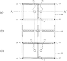
図22および図23は特許文献1に示す従来の血流計の光学センサの構成を示す図であり、図22(a)は上面図、図22(b)は図22(a)のA−A’断面図、図23(a)は図22(a)のB−B’断面図、図23(b)は図22(a)のC−C’断面図である。図22(a)、(b)に示すように従来の光学センサは、シリコン基板321、電極322、電極324、レーザダイオード361、フォトダイオード325及びカバー基板326を含む。
22 and FIG. 23 are diagrams showing the configuration of the optical sensor of the conventional blood flow meter shown in Patent Document 1, FIG. 22 (a) is a top view, and FIG. 22 (b) is an A- in FIG. 22 (a). FIG. 23A is a sectional view taken along the line BB ′ of FIG. 22A, and FIG. 23B is a sectional view taken along the line CC ′ of FIG. 22A. As shown in FIGS. 22A and 22B, the conventional optical sensor includes a
シリコン基板321は傾斜面に囲まれた2つの凹部を有している。シリコン基板321には前記凹部の外側からそれぞれの前記凹部内へ向けて電極322及び電極324が形成されている。レーザダイオード361は面発光型のレーザダイオードであり、フォトダイオード325は面入射型のフォトダイオードである。カバー基板326は光を透過する合成石英で形成される。図23に示すように、カバー基板326は屈折レンズ362と遮光膜331を有している。遮光膜331にはカバー基板326の両面に形成され、光がカバー基板を透過できるピンホールがある。
The
レーザダイオード361はシリコン基板321の前記凹部の一つに配置される。レーザダイオード361は、はんだ膜(図示せず)で電極322にボンディングされる。さらに、レーザダイオード361の発光部側の面と電極322とがワイヤ329で接続される。
同様にフォトダイオード325もシリコン基板321の前記凹部の他方に配置され、電極324と接続される。フォトダイオード325が配置される前記凹部の傾斜面を含む表面には遮光膜327が貼り付けられている。
The
Similarly, the
図23に示すように、カバー基板326は、屈折レンズ362がレーザダイオード361の配置される凹部を、遮光膜331がフォトダイオード325の配置される凹部を覆うようにシリコン基板321上に配置される。
As shown in FIG. 23, the
図23(a)に示すように、従来の光学センサは、カバー基板326の屈折レンズ362通じて、レーザダイオード361からの光を外部の被検体へ照射する。一方、図23(b)に示すように、従来の光学センサは、被検体へ照射した光の散乱光を遮光膜331に作られたピンホールを通じてフォトダイオード325で受光する。
As shown in FIG. 23A, the conventional optical sensor irradiates light from the
光学センサが受光した散乱光には、静止した生体組織による反射光と生体組織の毛細血管中を移動している赤血球(散乱粒子)による反射光が含まれる。赤血球による反射光の振動数は血流に応じてドップラーシフトをしており、静止した生体組織による反射光と干渉を起こす。前記干渉を検出(ヘテロダイン検波)することで血流量、血液量、血流速度、脈拍等の生体情報を計測することができる。このように、光の干渉を利用して生体情報を測定する方法を以下の説明でドップラーシフト法として示す。ドップラーシフト法の測定原理は、例えば、非特許文献1に記載されている。具体的には、血流速度は前記干渉光を周波数解析して測定でき、散乱光の強度で血流量を測定することができる。また、血流速度と血液量の積で血流量が求められる。 The scattered light received by the optical sensor includes reflected light from a stationary living tissue and reflected light from red blood cells (scattering particles) moving in the capillary of the living tissue. The frequency of reflected light from red blood cells is Doppler shifted according to the blood flow, causing interference with the reflected light from stationary biological tissue. By detecting the interference (heterodyne detection), biological information such as blood flow volume, blood volume, blood flow velocity, and pulse can be measured. Thus, a method for measuring biological information using light interference will be described as a Doppler shift method in the following description. The measurement principle of the Doppler shift method is described in Non-Patent Document 1, for example. Specifically, the blood flow velocity can be measured by frequency analysis of the interference light, and the blood flow rate can be measured by the intensity of the scattered light. Further, the blood flow volume is obtained by the product of the blood flow velocity and the blood volume.
しかし、血流計の光学センサは被検体と接触するため、光学センサのカバー基板の遮光膜が劣化して剥離すれば測定精度が低下してしまう。そのため、前記遮光膜には被検体と接触しても劣化して剥離しない程度の耐久性が求められる。また、シリコン基板の凹部にレーザダイオード及びフォトダイオードを収めてカバー基板で覆うため、シリコン基板の凹部はレーザダイオード及びフォトダイオードの高さより深い深さまでウエット異方性エッチングでエッチングすることが求められた。さらに、凹部への配線には、凹部での段差での断線を防止することが求められていた。これらの要求を満たすため光学センサの製造工程が複雑になり、従来の光学センサは製造コストが増大するという課題を有していた。 However, since the optical sensor of the blood flow meter is in contact with the subject, if the light shielding film on the cover substrate of the optical sensor is deteriorated and peeled off, the measurement accuracy is lowered. For this reason, the light-shielding film is required to have such durability that it does not deteriorate and peel off even when it comes into contact with the subject. Further, since the laser diode and the photodiode are accommodated in the concave portion of the silicon substrate and covered with the cover substrate, the concave portion of the silicon substrate is required to be etched by wet anisotropic etching to a depth deeper than the height of the laser diode and the photodiode. . Furthermore, the wiring to the concave portion has been required to prevent disconnection at a step in the concave portion. In order to satisfy these requirements, the manufacturing process of the optical sensor becomes complicated, and the conventional optical sensor has a problem that the manufacturing cost increases.
一方、レーザダイオードとフォトダイオードとはカバー基板を共通しており、レーザダイオードからの光の一部がカバー基板内を通過してしまい、レーザダイオードがその光を受光することでレーザダイオードの出力信号にノイズを生じていた。従来の光学センサには、生体情報を高精度に測定するために前記ノイズを低減しなければならないという課題があった。 On the other hand, the laser diode and the photodiode share the same cover substrate, and a part of the light from the laser diode passes through the cover substrate, and the laser diode receives the light so that the output signal of the laser diode Was producing noise. The conventional optical sensor has a problem that the noise must be reduced in order to measure biological information with high accuracy.
本発明は上記課題を解決するためになされたもので、低コストで容易に製造ができかつ高精度な測定ができる光学センサ及び生体情報測定装置を提供することを目的とする。 The present invention has been made to solve the above-described problems, and an object of the present invention is to provide an optical sensor and a biological information measuring apparatus that can be easily manufactured at low cost and can perform high-accuracy measurement.
前記目的を達成するために、本発明に係る光学センサは、絶縁基板上に搭載した発光素子及び受光素子を光が通過する2つの開口部を有するキャップで覆うこととした。 In order to achieve the above object, an optical sensor according to the present invention covers a light emitting element and a light receiving element mounted on an insulating substrate with a cap having two openings through which light passes.
具体的には、本発明は、外部への出射光を発生する発光素子と、外部からの散乱光を受光する受光素子と、前記発光素子及び前記受光素子を表面に搭載する絶縁基板と、前記絶縁基板上で前記発光素子及び前記受光素子を覆う不透明なキャップと、を備える光学センサであって、前記キャップは、前記発光素子からの出射光の一部を前記光学センサの外部へ通過させる第一開口部及び前記発光素子からの光が前記光学センサの外部で散乱した散乱光の一部を通過させて前記受光素子に受光させる第二開口部を有することを特徴とする光学センサである。 Specifically, the present invention includes a light emitting element that generates outgoing light to the outside, a light receiving element that receives scattered light from the outside, an insulating substrate on which the light emitting element and the light receiving element are mounted, And an opaque cap that covers the light emitting element and the light receiving element on an insulating substrate, wherein the cap allows a part of the light emitted from the light emitting element to pass outside the optical sensor. An optical sensor comprising: a first opening and a second opening for allowing the light receiving element to receive a part of the scattered light scattered from outside the optical sensor through the light from the light emitting element.
本発明に係る光学センサは、前記発光素子及び前記受光素子を電気配線パタンを施しただけの安価な平面の基板上に設置し、前記発光素子及び前記受光素子を覆うように前記キャップを設置した構造である。 In the optical sensor according to the present invention, the light-emitting element and the light-receiving element are installed on an inexpensive flat substrate provided with an electric wiring pattern, and the cap is installed so as to cover the light-emitting element and the light-receiving element. Structure.
前記キャップは不透明のため、従来のカバー基板のような遮光膜の形成工程が不要である。また、前記キャップが前記絶縁基板上に配置した発光素子と受光素子とを覆うように配置されるため、前記絶縁基板にエッチングで凹部を形成する工程が不要である。さらに、前記絶縁基板には凹部がないため、前記発光素子や前記受光素子への電気配線の断線を防止する工程も不要である。そのため、本発明に係る光学センサの製造は、従来の光学センサの製造に必要であった工程を省略することができ、製造コストを低減することができる。 Since the cap is opaque, there is no need for a light shielding film forming step as in a conventional cover substrate. In addition, since the cap is disposed so as to cover the light emitting element and the light receiving element disposed on the insulating substrate, a step of forming a recess in the insulating substrate by etching is not necessary. Furthermore, since the insulating substrate does not have a concave portion, a step of preventing disconnection of the electric wiring to the light emitting element and the light receiving element is unnecessary. Therefore, the manufacturing of the optical sensor according to the present invention can omit the steps necessary for manufacturing the conventional optical sensor and can reduce the manufacturing cost.
一方、前記キャップには遮光膜が無いため、遮光膜の劣化による剥離が無く測定精度の低下がない。さらに、前記キャップでは、従来のカバー基板のように発光素子からの光がカバー基板内を通過することがないため、受光素子が受光する被検体を介さない光を低減することができる。そのため、本発明に係る光学センサは、前記受光素子からの信号のノイズを低減でき、測定精度が向上する。 On the other hand, since the cap does not have a light shielding film, there is no peeling due to deterioration of the light shielding film, and there is no decrease in measurement accuracy. Further, in the cap, since light from the light emitting element does not pass through the cover substrate unlike a conventional cover substrate, light that does not pass through the subject received by the light receiving element can be reduced. Therefore, the optical sensor according to the present invention can reduce the noise of the signal from the light receiving element, and the measurement accuracy is improved.
従って、本発明は、低コストで容易に製造ができ且つ高精度な測定ができる光学センサを提供することができる。 Therefore, the present invention can provide an optical sensor that can be easily manufactured at low cost and can perform high-precision measurement.
本発明に係る光学センサの前記発光素子は、前記絶縁基板の法線方向に出射光を出射する面発光型であり、前記受光素子は、前記絶縁基板の法線方向からの散乱光を受光する面入射型であり、前記キャップの前記第一開口部は、前記発光素子の出射光の出射方向にある第一孔であり、前記キャップの前記第二開口部は、前記受光素子に対して前記受光素子が散乱光を受光できる方向にある第二孔であることを特徴とする。 The light emitting element of the optical sensor according to the present invention is a surface-emitting type that emits outgoing light in a normal direction of the insulating substrate, and the light receiving element receives scattered light from the normal direction of the insulating substrate. It is a surface incident type, and the first opening of the cap is a first hole in the emission direction of the emitted light of the light emitting element, and the second opening of the cap is the first opening with respect to the light receiving element. The light receiving element is a second hole in a direction in which scattered light can be received.
本発明は、面発光型発光素子及び面入射型受光素子を搭載し、低コストで容易に製造ができ且つ高精度な測定ができる光学センサを提供することができる。 The present invention can provide an optical sensor that is equipped with a surface-emitting light-emitting element and a surface-incident light-receiving element, can be easily manufactured at low cost, and can perform highly accurate measurement.
本発明に係る光学センサにおいて、前記キャップは、第一孔の中心と第二孔の中心との中間点を通る前記絶縁基板の垂線を二回軸とする回転対称形状であることが好ましい。二回軸に対する回転対称形状とは前記軸のまわりに180度回転移動させても形状が変わらない形状をいう。以下の説明において「二回軸に対する回転対称形状」を「二回回転対称形状」として示す。 In the optical sensor according to the present invention, it is preferable that the cap has a rotationally symmetric shape with a perpendicular of the insulating substrate passing through an intermediate point between the center of the first hole and the center of the second hole as a two-fold axis. The rotationally symmetric shape with respect to the two-fold axis means a shape that does not change even if it is rotated 180 degrees around the axis. In the following description, “a rotationally symmetric shape with respect to the two-fold axis” is indicated as “a two-fold rotationally symmetric shape”.
前記絶縁基板に前記キャップを実装する実装工程は、前記キャップの表裏を合わせる表裏確認ステップと前記キャップの向きを合わせる方向確認ステップとからなる。前記絶縁基板側から見たキャップの形状が二回回転対称形状でなければ、前記方向確認ステップでキャップと前記絶縁基板とを装着する際に向きを正しく合わせるのに最大180度回転させる必要がある。一方、前記絶縁基板側から見たキャップの形状が二回回転対称形状であれば最大でも90度回転で前記キャップを前記絶縁基板に実装が可能になる。 The mounting process of mounting the cap on the insulating substrate includes a front / back confirmation step for aligning the front and back of the cap and a direction confirmation step for aligning the direction of the cap. If the shape of the cap viewed from the insulating substrate side is not a rotationally symmetric shape twice, it is necessary to rotate the cap 180 degrees at the maximum in order to correctly align the cap and the insulating substrate in the direction confirmation step. . On the other hand, if the shape of the cap viewed from the insulating substrate side is a two-fold rotationally symmetric shape, the cap can be mounted on the insulating substrate at a maximum of 90 degrees.
従って、本発明は、低コストで容易に製造ができ且つ高精度な測定ができる光学センサを提供することができる。 Therefore, the present invention can provide an optical sensor that can be easily manufactured at low cost and can perform high-precision measurement.
本発明に係る光学センサにおいて、前記キャップは、第一孔の中心と第二孔の中心との中間点を通る前記絶縁基板と平行な平行線を二回軸とする回転対称形状であることが好ましい。 In the optical sensor according to the present invention, the cap may have a rotationally symmetric shape with a parallel line parallel to the insulating substrate passing through an intermediate point between the center of the first hole and the center of the second hole as a two-fold axis. preferable.
前記絶縁基板面と平行な方向から見た前記キャップの形状が二回回転対称形状でなければ、前記表裏確認ステップで最大180度回転させる必要がある。一方、前記絶縁基板面と平行な方向から見たキャップの形状が二回回転対称であれば最大でも90度回転で前記キャップを前記絶縁基板に実装が可能になる。 If the shape of the cap viewed from a direction parallel to the surface of the insulating substrate is not a rotationally symmetric shape twice, it is necessary to rotate the cap by 180 degrees at the front and back confirmation step. On the other hand, if the shape of the cap viewed from a direction parallel to the surface of the insulating substrate is rotationally symmetrical twice, the cap can be mounted on the insulating substrate with a maximum rotation of 90 degrees.
従って、本発明は、低コストで容易に製造ができ且つ高精度な測定ができる光学センサを提供することができる。 Therefore, the present invention can provide an optical sensor that can be easily manufactured at low cost and can perform high-precision measurement.
本発明に係る光学センサの前記発光素子は、前記絶縁基板の面と水平な方向に出射光を端面から出射する端面発光型であり、前記受光素子は、前記絶縁基板の面と水平な方向からの散乱光を端面で受光する端面入射型であり、前記キャップの前記第一開口部は、前記発光素子に対して前記発光素子の出射光の出射方向にあり、前記キャップの前記第二開口部は、前記受光素子に対して前記受光素子が散乱光を受光できる方向にあることを特徴とする。 The light emitting element of the optical sensor according to the present invention is an end face light emitting type that emits outgoing light from an end face in a direction parallel to the surface of the insulating substrate, and the light receiving element is from a direction parallel to the surface of the insulating substrate. The first opening of the cap is in the emission direction of the emitted light of the light emitting element with respect to the light emitting element, and the second opening of the cap Is characterized in that the light receiving element is in a direction capable of receiving scattered light with respect to the light receiving element.
本発明に係る光学センサの前記発光素子は、前記絶縁基板の法線方向に出射光を出射する面発光型であり、前記受光素子は、前記絶縁基板の面と水平な方向からの散乱光を端面で受光する端面入射型であり、前記キャップは、前記発光素子の出射光の方向を前記絶縁基板の面と水平な方向へ変換する光路変換素子をさらに有しており、前記キャップの前記第一開口部は、前記発光素子の出射光が前記キャップの前記光路変換素子で変換された光路方向にあり、前記キャップの前記第二開口部は、前記受光素子に対して前記受光素子が散乱光を受光できる方向にあることを特徴とする。 The light emitting element of the optical sensor according to the present invention is a surface-emitting type that emits outgoing light in a normal direction of the insulating substrate, and the light receiving element emits scattered light from a direction parallel to the surface of the insulating substrate. The cap is of an end surface incident type that receives light at an end surface, and the cap further includes an optical path conversion element that converts a direction of emitted light of the light emitting element into a direction parallel to a surface of the insulating substrate, The one opening is in an optical path direction in which the light emitted from the light emitting element is converted by the optical path conversion element of the cap, and the second opening of the cap has the light receiving element scattered light with respect to the light receiving element. It is in the direction which can receive light.
本発明に係る光学センサの前記発光素子は、前記絶縁基板の面と水平な方向に出射光を端面から出射する端面発光型であり、前記受光素子は、前記絶縁基板の法線方向からの散乱光を受光する面入射型であり、前記キャップは、前記絶縁基板の面と水平な方向である散乱光の方向を前記絶縁基板の法線方向へ変換する光路変換素子をさらに有しており、前記キャップの前記第一開口部は、前記発光素子に対して前記発光素子の出射光の出射方向にあり、前記キャップの前記第二開口部は、前記キャップの前記光路変換素子に対して前記キャップの前記光路変換素子に散乱光を照射できる方向にあり、前記キャップの光路変換素子は、前記第二開口部を通過した散乱光の光路を変換して前記受光素子に受光させることを特徴とする。 The light emitting element of the optical sensor according to the present invention is an end face light emitting type that emits outgoing light from an end face in a direction parallel to the surface of the insulating substrate, and the light receiving element is scattered from the normal direction of the insulating substrate. It is a surface incidence type that receives light, and the cap further includes an optical path conversion element that converts the direction of scattered light, which is a direction parallel to the surface of the insulating substrate, into the normal direction of the insulating substrate, The first opening of the cap is in an emission direction of emitted light of the light emitting element with respect to the light emitting element, and the second opening of the cap is with respect to the optical path conversion element of the cap. The optical path conversion element of the cap is in a direction in which scattered light can be irradiated, and the optical path conversion element of the cap converts the optical path of the scattered light that has passed through the second opening and causes the light receiving element to receive the light. .
本発明は、前記絶縁基板に水平な方向に出射光を出射し、前記絶縁基板に水平な方向からの散乱光を受光し、低コストで容易に製造ができ且つ高精度な測定ができる光学センサを提供することができる。また、適宜光路変換素子を用いることで面発光型発光素子や面入射型受光素子も利用することができる。 The present invention provides an optical sensor that emits outgoing light in a horizontal direction on the insulating substrate, receives scattered light from the horizontal direction on the insulating substrate, can be easily manufactured at low cost, and can perform highly accurate measurement. Can be provided. In addition, a surface light emitting element or a surface incident light receiving element can also be used by appropriately using an optical path conversion element.
本発明に係る光学センサの前記キャップは、前記発光素子と前記受光素子との間を仕切り、前記受光素子が前記発光素子からの出射光を直接受光することを防止する仕切り板をさらに有してもよい。 The cap of the optical sensor according to the present invention further includes a partition plate that partitions between the light emitting element and the light receiving element and prevents the light receiving element from directly receiving light emitted from the light emitting element. Also good.
前記仕切り板は前記キャップ内において前記発光素子と前記受光素子との間を仕切るため、前記キャップ内で反射した前記発光素子からの光を前記受光素子が受光することを防止することができる。前記受光素子は前記キャップ内で反射した前記発光素子からの光によるノイズを低減した信号を出力することができる。また、前記仕切り板を前記キャップの前記絶縁基板側に接着するだけなので、前記キャップを容易に製造できる。あるいは仕切り板を初めから有するキャップを製造することもできる。仕切り板を接着する工程を省略することができ、前記キャップを容易に製造できる。 Since the partition plate partitions the light emitting element and the light receiving element in the cap, it is possible to prevent the light receiving element from receiving light from the light emitting element reflected in the cap. The light receiving element can output a signal in which noise due to light from the light emitting element reflected in the cap is reduced. In addition, since the partition plate is simply bonded to the insulating substrate side of the cap, the cap can be easily manufactured. Or the cap which has a partition plate from the beginning can also be manufactured. The step of bonding the partition plate can be omitted, and the cap can be easily manufactured.
従って、本発明は、低コストで容易に製造ができ且つ高精度な測定ができる光学センサを提供することができる。 Therefore, the present invention can provide an optical sensor that can be easily manufactured at low cost and can perform high-precision measurement.
本発明に係る光学センサにおいて、前記絶縁基板は、前記発光素子及び前記受光素子が搭載される側の表面に電気配線をさらに搭載し、前記キャップは、導電性材料で形成され、前記絶縁体基板上の前記電気配線のうち前記受光素子のカソードに接続している電気配線と接触しており、前記受光素子のカソードと同電位であってもよい。 In the optical sensor according to the present invention, the insulating substrate further includes an electrical wiring on a surface on which the light emitting element and the light receiving element are mounted, the cap is formed of a conductive material, and the insulator substrate It may be in contact with the electrical wiring connected to the cathode of the light receiving element among the electrical wirings above, and may have the same potential as the cathode of the light receiving element.
また、本発明に係る光学センサにおいて、前記絶縁基板は、前記発光素子及び前記受光素子が搭載される側の表面に電気配線をさらに搭載し、前記キャップは、導電性材料で形成され、前記絶縁体基板上の前記電気配線のうち前記発光素子のカソードに接続している電気配線と接触しており、前記発光素子のカソードと同電位であってもよい。 In the optical sensor according to the present invention, the insulating substrate further includes an electrical wiring on a surface on which the light emitting element and the light receiving element are mounted, the cap is formed of a conductive material, and the insulating substrate The electrical wiring on the body substrate may be in contact with the electrical wiring connected to the cathode of the light emitting element, and may have the same potential as the cathode of the light emitting element.
前記受光素子の信号は増幅器で増幅されるまでは微弱であり、外来の電磁ノイズの影響を受けやすい。導電性の前記キャップは前記発光素子又は/及び前記受光素子のカソードと同電位になるため、外来の電磁ノイズを防いで前記受光素子からの信号のSN比を向上させることができる。 The signal of the light receiving element is weak until amplified by an amplifier, and is easily affected by external electromagnetic noise. Since the conductive cap has the same potential as the light emitting element and / or the cathode of the light receiving element, it is possible to prevent external electromagnetic noise and improve the signal-to-noise ratio of the signal from the light receiving element.
従って、本発明は、低コストで容易に製造ができ且つ高精度な測定ができる光学センサを提供することができる。 Therefore, the present invention can provide an optical sensor that can be easily manufactured at low cost and can perform high-precision measurement.
本発明に係る光学センサは、前記キャップで覆われた前記絶縁基板の表面に、前記受光素子から出力される信号を増幅する増幅回路をさらに備え、前記増幅回路のカソードは前記受光素子のカソードが接続する電気配線に接続され且つ前記受光素子から出力される信号を前記増幅回路に結合する配線の長さは0.1mm以上10mm以下としてもよい。 The optical sensor according to the present invention further includes an amplification circuit for amplifying a signal output from the light receiving element on the surface of the insulating substrate covered with the cap, and the cathode of the amplification circuit is the cathode of the light receiving element. The length of the wiring connected to the electric wiring to be connected and coupling the signal output from the light receiving element to the amplifier circuit may be 0.1 mm or more and 10 mm or less.
前記受光素子の信号は増幅器で増幅されるまでは微弱であり、外来の電磁ノイズの影響を受けやすい。そこで、前記キャップ内において、前記受光素子に隣接して前記増幅回路を配置することとした。外来の電磁ノイズによる影響が大きい前記受光素子から前記増幅回路までの距離を短くし、前記キャップ内で受光素子からの信号を増幅することで、前記増幅器からの信号のSN比を向上できる。前記増幅回路は前記発光素子及び前記受光素子と同様前記絶縁基板上に配置するだけなので、本発明に係る光学センサを容易に製造できる。 The signal of the light receiving element is weak until amplified by an amplifier, and is easily affected by external electromagnetic noise. Therefore, the amplifier circuit is disposed adjacent to the light receiving element in the cap. The signal-to-noise ratio of the signal from the amplifier can be improved by shortening the distance from the light receiving element to the amplifier circuit that is greatly affected by external electromagnetic noise and amplifying the signal from the light receiving element in the cap. Since the amplifier circuit is only disposed on the insulating substrate in the same manner as the light emitting element and the light receiving element, the optical sensor according to the present invention can be easily manufactured.
従って、本発明は、低コストで容易に製造ができ且つ高精度な測定ができる光学センサを提供することができる。 Therefore, the present invention can provide an optical sensor that can be easily manufactured at low cost and can perform high-precision measurement.
本発明に係る光学センサにおいて、前記キャップは前記絶縁体基板側に突起を有し、前記絶縁体基板は、前記キャップの前記突起が挿入されて前記キャップの位置決めをする穴又は孔を有することが好ましい。 In the optical sensor according to the present invention, the cap has a protrusion on the insulator substrate side, and the insulator substrate has a hole or a hole into which the protrusion of the cap is inserted to position the cap. preferable.
前記キャップと前記絶縁基板との相対位置が変化すると、前記発光素子と前記第一孔との相対位置及び前記受光素子と前記第二孔との相対位置が変化するため、光学センサ間で測定精度に差を生ずる。そこで、前記キャップに予め位置合わせ用の前記突起を設けておき、前記絶縁体基板に予め前記位置合わせ用の穴又は孔を設けておくこととした。前記キャップを前記絶縁体基板に実装する際に、前記キャップの前記突起を前記絶縁基板の前記孔又は前記穴に挿入することで両者間の位置を容易且つ高精度に合わせることができる。また、予め定められた箇所に前記突起及び前記穴又は前記孔を有するため、光学センサ間で前記キャップと前記絶縁基板との相対位置が一定になるため、光学センサの測定精度を一定に保つことができる。 When the relative position between the cap and the insulating substrate changes, the relative position between the light emitting element and the first hole and the relative position between the light receiving element and the second hole change. Make a difference. Therefore, the positioning projections are provided in advance on the cap, and the positioning holes or holes are provided in advance on the insulator substrate. When the cap is mounted on the insulator substrate, the protrusions of the cap are inserted into the holes or the holes of the insulating substrate, so that the position between the two can be adjusted easily and with high accuracy. In addition, since the protrusion and the hole or the hole are provided at a predetermined location, the relative position between the cap and the insulating substrate is constant between the optical sensors, so that the measurement accuracy of the optical sensor is kept constant. Can do.
従って、本発明は、低コストで容易に製造ができ且つ高精度な測定ができる光学センサを提供することができる。 Therefore, the present invention can provide an optical sensor that can be easily manufactured at low cost and can perform high-precision measurement.
前記目的を達成するために、本発明に係る生体情報測定装置は前記光学センサを備えている。 In order to achieve the object, a biological information measuring apparatus according to the present invention includes the optical sensor.
具体的には、本発明は、前記光学センサと、前記発光素子を駆動する回路と、前記光学センサからの信号を処理して生体情報に関する値を計算するデジタル信号プロセッサと、を含む集積回路を備える生体情報測定装置である。 Specifically, the present invention includes an integrated circuit including the optical sensor, a circuit that drives the light emitting element, and a digital signal processor that processes a signal from the optical sensor and calculates a value related to biological information. It is a biological information measuring device provided.
本発明に係る生体情報測定装置は、本発明に係る光学センサを使用しているため、生体情報を高精度に測定することができる。さらに、本発明に係る生体情報測定装置は、製造が容易な光学センサを使用しているため低コストで製造することができる。 Since the biological information measuring device according to the present invention uses the optical sensor according to the present invention, biological information can be measured with high accuracy. Furthermore, the biological information measuring device according to the present invention can be manufactured at low cost because it uses an optical sensor that is easy to manufacture.
本発明に係るセンサチップは、キャップの側面に第一開口部及び第二開口部を有する光学センサと、長手方向の一端に前記光学センサを搭載する短冊形の回路基板と、を備えるセンサチップであって、前記光学センサは、前記発光素子の出射光を前記回路基板の他端から一端の方向へ出射することを特徴とする。 A sensor chip according to the present invention is a sensor chip comprising: an optical sensor having a first opening and a second opening on a side surface of a cap; and a strip-shaped circuit board on which the optical sensor is mounted at one end in a longitudinal direction. The optical sensor emits light emitted from the light emitting element in the direction from the other end to the one end of the circuit board.
また、本発明に係るセンサチップは、キャップの側面に第一開口部及び第二開口部を有する光学センサと、長手方向の一端に前記光学センサを搭載する短冊形の回路基板と、を備えるセンサチップであって、前記光学センサは、前記発光素子の出射光を前記回路基板の面と平行であり、且つ前記回路基板の長手方向と直交する方向へ出射することを特徴とする。 In addition, a sensor chip according to the present invention includes an optical sensor having a first opening and a second opening on a side surface of a cap, and a strip-shaped circuit board on which the optical sensor is mounted at one end in a longitudinal direction. The optical sensor emits light emitted from the light emitting element in a direction parallel to the surface of the circuit board and perpendicular to the longitudinal direction of the circuit board.
短冊状の回路基板をプローブとすれば、光学センサを被検体の奥や狭い箇所に入れることができ、当該箇所の生体情報を取得することができる。 If a strip-shaped circuit board is used as a probe, the optical sensor can be placed in the back or narrow part of the subject, and biological information of the part can be acquired.
以上の説明のように、本発明は、低コストで容易に製造ができ且つ高精度な測定ができる光学センサ及び生体情報測定装置を提供することができる。 As described above, the present invention can provide an optical sensor and a biological information measuring apparatus that can be easily manufactured at low cost and can perform high-accuracy measurement.
添付の図面を参照して本発明の実施の形態を説明する。以下に説明する実施の形態は本発明の構成の例であり、本発明は、以下の実施の形態に制限されるものではない。なお、本明細書及び図面において符号が同じものは、相互に同一のものを示すものとする。 Embodiments of the present invention will be described with reference to the accompanying drawings. The embodiment described below is an example of the configuration of the present invention, and the present invention is not limited to the following embodiment. In the present specification and drawings, the same reference numerals denote the same ones.
(実施の形態1)
本実施形態は、外部への出射光を発生する発光素子と、外部からの散乱光を受光する受光素子と、前記発光素子及び前記受光素子を表面に搭載する絶縁基板と、前記絶縁基板上で前記発光素子及び前記受光素子を覆う不透明なキャップと、を備える光学センサであって、前記キャップは、前記発光素子からの出射光の一部を前記光学センサの外部へ通過させる第一孔及び前記発光素子からの光が前記光学センサの外部で散乱した散乱光の一部を通過させて前記受光素子に受光させる第二孔を有することを特徴とする光学センサである。
(Embodiment 1)
In the present embodiment, a light emitting element that generates outgoing light, a light receiving element that receives scattered light from the outside, an insulating substrate on which the light emitting element and the light receiving element are mounted, and an insulating substrate An opaque cap that covers the light emitting element and the light receiving element, wherein the cap has a first hole through which a part of light emitted from the light emitting element passes outside the optical sensor; and An optical sensor comprising a second hole through which a part of scattered light scattered from the outside of the optical sensor is received by the light receiving element.
本実施形態に係る光学センサ501の概略図を図1に示す。光学センサ501は絶縁基板11、キャップ13、発光素子15及び受光素子17を備える。図1(a)は光学センサ501をキャップ13側から見た上面図であり、図1(b)は図1(a)のA−A’での切断面の図である。図5から図9において同様である。
A schematic diagram of an
絶縁基板11の材質は、ガラスエポキシ樹脂、フッ素樹脂、セラミック等の絶縁物が例示できる。絶縁基板11の表面には図2から図4に示す電気配線21aから電気配線21eまでの電気配線パタンが形成される。図2から図4までで使用されている符号は図1で説明した符号と同じ部品を示す。電気配線21aから電気配線21eはワイヤボンディング可能な金属であり、メッキで作製された厚さ5μmのNi上に厚さ0.3μmのAuを積層した二層構造などの金属膜が例示できる。絶縁基板11は公知のプリント回路基板を製造する技術で製造することができる。なお、絶縁基板11は表面に窒化膜や酸化膜を積層したシリコン基板でもよい。絶縁基板11が前記シリコン基板の場合、公知の半導体製造方法によって表面に金属の電気配線パタンを形成することができる。なお、図1の絶縁基板11の電気配線パタンは図2に示される電気配線パタンである。
Examples of the material of the insulating
発光素子15は外部への出射光を発生する。発光素子15として面発光型の半導体レーザが好ましい。半導体レーザとしては、波長0.6μmから1.6μmの光を発生させる化合物半導体を利用することができる。特に、波長1.3μmの光は、従来の市販品で多く使われている波長780nmの光に比べ、皮膚組織の透過率が高く、皮下深くの血流を検出でき、そのためSN比の良い血流波形を計測できる。
The
受光素子17は外部からの散乱光を受光し、散乱光の光強度に応じた散乱光強度信号を出力する。受光素子17としてフォトダイオードが例示される。散乱光は発光素子15からのレーザ光が被検体内で散乱した光であるため、フォトダイオードの種類は発光素子15の種類に応じて選択される。
The
キャップ13は第一孔19a及び第二孔19bを有する。第一孔19aの大きさは、300μm−1000μm程度であり、第二孔19bの大きさは100μm−500μm程度であるが、本実施例では双方ともに500μmとして説明する。キャップ13は不透明なプラスチックや金属で形成される。キャップ13がプラスチックで形成される場合、表面を金属のような導電性膜で被覆してもよい。キャップ13をプラスチック射出成型の方法で形成し金属薄膜で表面を被覆すれば大量生産が可能になり、光学センサの製造コストを低減することができる。本実施例では、キャップ13の素材はアルミニウムとして説明する。
The
図2に示すように、発光素子15のカソード(発光面と反対の側)は電気配線21b上にはんだ膜を介して接続され、発光素子15は絶縁基板11上に実装される。発光素子15のアノード(発光面側)はワイヤ23で電気配線21aと接続される。受光素子17も発光素子15と同様に絶縁基板11上に実装される。なお、受光素子17のアノードは電気配線21dであり、カソードは電気配線21cである。
As shown in FIG. 2, the cathode (the side opposite to the light emitting surface) of the
キャップ13は発光素子15及び受光素子17を覆うように絶縁基板11上に実装される。キャップ13の絶縁基板11上の位置は、発光素子15からの光が第一孔19aを通過して外部の被検体を照射でき、外部からの光が第二孔19bを通過して受光素子17が受光できる位置とする。
The
キャップ13は導電性を有するため、キャップ13と電気配線21と電気的に導通しないようにキャップ13と電気配線21aから電気配線21dとの接触点はレジスト等の絶縁膜25で覆われている。キャップ13が導電性を有さない場合、絶縁膜25は不要である。
Since the
光学センサ501は、外部の駆動回路(図示せず)から発光素子15のアノードが接続する電気配線21に電流が供給され、発光素子15のカソードが接続する電気配線21から前記駆動回路へ電流が出ていくことで発光素子15は発光し、第一孔19aを通じて外部の被検体に光を照射することができる。なお、発光素子15からの光のうちキャップ13内で反射する光を低減するため、キャップ13の発光素子15を覆う側(キャップ13の内側)に反射防止膜を付してもよい。
In the
一方、受光素子17は、外部からの光のうち生体情報測定に必要な光のみを第二孔19bを通じて受光し、電気信号に変換して電気配線21cに出力する。従って、光学センサ501は外部の被検体で散乱した散乱光に対応する電気信号を電気配線21cから出力する。
On the other hand, the
光学センサ501の製造において、絶縁基板11のエッチングが不要、キャップ13に遮光膜の形成が不要である。さらに、絶縁基板11に段差がないため電気配線パタンの形成が容易である。従って、発光素子15及び受光素子17を電気配線パタンを施しただけの安価な平面の絶縁基板11上に実装し、さらに発光素子15及び受光素子17を覆うようにキャップ13を実装するだけであり、光学センサ501は低コストで製造できる。
In the manufacture of the
また、光学センサ501は、キャップ13に遮光膜が無いため、遮光膜の劣化による剥離が無く測定精度の低下がない。さらに、キャップ13は不透明のため、従来のカバー基板のように発光素子15からの光がカバー基板内を通過することがなく、光学センサ501は、受光素子17が受光する被検体を介さない光を低減することができる。そのため、光学センサ501は高精度に被検体の生体情報を測定することができる。
Further, since the
本実施形態に係る光学センサ505の概略図を図5に示す。光学センサ501と図1の光学センサ501との違いは、光学センサ501の電気配線21cの表面が絶縁膜25で被覆されていない点である。図5において、図1で使用した符号と同じ符号は同じ部品を示す。電気配線21cの表面は絶縁膜25で被覆されていないためキャップ13と電気配線21cとが接触し、キャップ13の電位は受光素子17のカソードの電位と等しくなる。キャップ13は受光素子17のカソードと等しい電位であるため、外来の電磁ノイズを防止する効果を有する。受光素子17が出力する信号は増幅器で増幅されるまでは非常に弱いため、外来の電磁ノイズの影響を受けやすい。従って、電気配線21cとキャップ13とを接触させることで受光素子17からの信号のSN比を向上させることができる。
FIG. 5 shows a schematic diagram of the
光学センサ505は図1の光学センサ501と同様に低コストで製造できるとともに、キャップ13の電磁ノイズ防止の効果により、光学センサ501よりさらに高精度に生体情報を測定することができる。
The
本実施形態に係る光学センサ506の概略図を図6に示す。光学センサ501と図1の光学センサ501との違いは、絶縁基板11の電気配線パタンが図3に示す電気配線パタンである点及び光学センサ501の電気配線21bの表面が絶縁膜25で被覆されていない点である。図6において、図1で使用した符号と同じ符号は同じ部品を示す。図6に示すように、電気配線21bの表面が絶縁膜25で被覆されていないため、キャップ13は発光素子15のカソードと電位が等しくなり、図5の光学センサ505で説明した効果と同様の効果を得られる。
FIG. 6 shows a schematic diagram of the
図5及び図6では、電気配線21b又は電気配線21cのいずれかの表面を絶縁膜25で被覆されない場合を示したが、電気配線21b及び電気配線21cの双方の表面が絶縁膜25で被覆されていなくてもよい。この場合であっても、図5の光学センサ505で説明した効果と同様の効果を得られる。
5 and 6 show the case where the surface of either the
さらに、絶縁基板11は図4に示す電気配線パタンを搭載してもよい。図4の電気配線パタンは電気配線21b及び電気配線21cがなく、発光素子15及び受光素子17のカソードが共通して接触する電気配線21eを有する。図4の電気配線パタンを搭載する絶縁基板11にキャップ13を搭載する場合、図1の光学センサ501で説明したように電気配線21a、21d及び21eのキャップ13との接触箇所を絶縁膜25で被覆してもよい。図4の電気配線パタンを搭載する絶縁基板11の光学センサも図1の光学センサ501と同様の効果を得られる。一方、図5の光学センサ505で説明したように電気配線21eの表面を絶縁膜25で被覆せず、キャップ13と接触させてもよい。図4の電気配線パタンを搭載する絶縁基板11の光学センサも図5の光学センサ505と同様の効果を得られる。
Further, the insulating
キャップ13は、発光素子15と受光素子17との間を仕切り、受光素子17が発光素子15からの出射光を直接受光することを防止する仕切り板75をさらに有してもよい。図7に仕切り板75を有するキャップ13を含む光学センサ507を示す。図7において、図1で使用した符号と同じ符号は同じ部品を示す。
The
仕切り板75はキャップ13と同じ素材であり不透明である。仕切り板75は絶縁基板11上の発光素子15と受光素子17との間を仕切るようにキャップ13の内側に配置される。キャップ13と絶縁基板11とで囲まれる空間は、仕切り板75により発光素子15が収まる小室と受光素子17が収まる小室に分けられる。
The
受光素子17で受光する光のうちドップラーシフト法による干渉成分は数100pW程度と非常に微弱である。そのため、キャップ13と絶縁基板11が作る空間内で反射した発光素子15からの光を受光素子17が受光すれば、該光の強度に前記干渉成分の強度が埋もれてしまい、受光素子17が出力する前記干渉成分の信号のSN比が悪くなる。従って、光学センサ507は、仕切り板75で発光素子15の小室と受光素子17の小室を分離したことで、発光素子15からの光を遮断でき、受光素子17が出力する信号のSN比を向上させ、精度よく生体情報を測定することができる。
Among the light received by the
キャップ13で覆われた絶縁基板11の表面に、受光素子17から出力される信号を増幅する増幅回路85をさらに備えてもよい。増幅回路85のカソードは受光素子17のカソードが接続する電気配線21cに接続され且つ受光素子17から出力される信号を増幅回路85に結合するワイヤ83の長さは0.1mm以上10mm以下である。図8に増幅回路85を備える光学センサ508を示す。図8において、図1で使用した符号と同じ符号は同じ部品を示し、説明のためキャップ13の一部を省略して記載している。
An
光学センサ508は、図4の電気配線パタンを利用し、受光素子17のカソードと増幅回路85のグラウンドとが電気配線21cを共通している。電気配線81aおよび電気配線81bは増幅回路85の電源供給用の配線であり、電気配線81c及び電気配線81dは増幅信号を出力する二本の端子である。さらに、受光素子17からの出力は、ワイヤ83で増幅回路85に入力される。このように受光素子17からの信号は絶縁基板11上の電気配線パタンを通らずに増幅回路85で増幅され、電気配線81c及び電気配線81dから出力される。
The
受光素子17、ワイヤ83及び増幅回路85は受光素子17のカソードと導電位であるキャップ13に覆われるため、増幅回路85は受光素子17からの信号を外部からの電磁ノイズを受ける前に増幅することができる。
Since the
さらに、増幅回路85からワイヤ87a及びワイヤ87bを通じて電気配線81c及び電気配線81dに出力される信号は既に増幅されているため、外部からのノイズの影響を受けにくく、SN比を向上させることができる。従って、光学センサ508は精度よく生体情報を測定することができる。
Furthermore, since the signals output from the
また、光学センサ508からの生体情報に関する信号は増幅されているので、光学センサ508の外部の増幅器において、ノイズの少ない信号を得ることができ、該増幅器を簡略化することができる。
In addition, since a signal related to biological information from the
図9に光学センサ509を示す。図9において、図1で使用した符号と同じ符号は同じ部品を示し、説明のためキャップ13の一部を省略して記載している。光学センサ509の絶縁基板11は図2に示す電気配線パタンを搭載する。増幅回路85のグランドと受光素子17のカソードとは共通の電気配線である。発光素子15のカソードと受光素子17のカソードが別の電気配線に接続しており、増幅回路85のグランドと発光素子15のカソードとを分離することができる。光学センサ509の増幅回路85は、発光素子15の電源に起因するノイズの影響を受けないため、SN比を向上させることができる。従って、光学センサ509は精度よく生体情報を測定することができる。
FIG. 9 shows an
図10は、光学センサと外部の増幅回路を搭載するセンサチップ610である。センサチップ610は、プリント回路基板91、増幅回路95及び光学センサ501を含む。
FIG. 10 shows a
センサチップ610は増幅回路95が形成されたプリント回路基板91上に光学センサ501をエポキシ等の絶縁性接着剤を用いて設置したものである。センサチップ610は光学センサ501に限らず、光学センサ505から光学センサ507を搭載できる。増幅回路95は、光学センサ501からの微弱な信号を増幅するため大きな増幅率を必要とし、オペアンプICを二段使用している(オペアンプ95a及びオペアンプ95b)。
The
プリント回路基板91には電極パッド93aから電極パッド93dが備えられている。電極パッド93aから電極パッド93dはそれぞれ光学センサの電気配線21aから電気配線21dがワイヤ97で電気的に接続される。さらに受光素子17のアノードが接続する電極パッド93dから増幅回路95(オペアンプ95a)までを電気配線99が接続する。
The printed
受光素子17が出力する信号は電気配線21d、ワイヤ97、電極パッド93d、電気配線99を通り、オペアンプ95a続いてオペアンプ95bで増幅され、外部に出力される。
A signal output from the
図10ではプリント回路基板91の一つの面に光学センサ501と増幅回路95とを搭載しているが、プリント回路基板91の一の面に光学センサ501、他の面に増幅回路95を搭載してもよい。プリント回路基板91の両面を利用することでプリント回路基板91を小型化することができ、センサチップ610を小型化できる。
In FIG. 10, the
図11はプリント回路基板91に図2で示す電気配線パタンを形成し、発光素子15、受光素子17及びキャップ13をプリント配線基板91に直接搭載したセンサチップ611である。図1の光学センサ501の説明と同様に発光素子15、受光素子17及びキャップ13をプリント配線基板91に搭載する。センサチップ611は図10のセンサチップ610と同様に動作する。センサチップ611は図10のセンサチップ610と比較して、光学センサ501をプリント回路基板91に貼り付ける工程や電気配線21aから電気配線21dと電極パッド93aから電極パッド93dとをワイヤボンディングする工程が不要になり製造コストを低減できる。プリント回路基板91に形成する電気配線パタンは図2に限らず図3及び図4でもよく、図8で説明した電気配線パタンとしてもよい。
FIG. 11 shows a
図12は、プリント回路基板91に図9で説明した光学センサ509を搭載したセンサチップ612である。センサチップ612は光学センサ509で既に増幅された信号が出力されるので増幅回路95をオペアンプ95bのみとすることができ、プリント回路基板91を小型化することができる。センサチップ612には図8の光学センサ508を搭載してもよい。
FIG. 12 shows a
図10から図12で説明したように、プリント回路基板91に光学センサ501、光学センサ505〜509のいずれかの光学センサを搭載することあるいはプリント回路基板91に直接電気配線パタンを形成して光学センサ501、光学センサ505〜509のいずれかの光学センサを構成することで、実装が容易であり製作コストを低減した測定精度の高いセンサチップを実現することができる。
As described with reference to FIGS. 10 to 12, the
(実施の形態2)
本実施形態は、前記キャップが前記絶縁体基板側に突起を有し、前記絶縁体基板が、前記キャップの前記突起が挿入されて前記キャップの位置決めをする穴又は孔を有することを特徴とする光学センサである。
(Embodiment 2)
In this embodiment, the cap has a projection on the insulator substrate side, and the insulator substrate has a hole or a hole for positioning the cap by inserting the projection of the cap. It is an optical sensor.
図13に他の実施形態である光学センサを示す。図13で使用されている符号は図1で説明した符号と同じ部品を示す。図13の光学センサと図1の光学センサ501との違いは、キャップ13が突起123を少なくとも2つ有していること及び絶縁基板11が孔121を有していることである。
FIG. 13 shows an optical sensor according to another embodiment. The reference numerals used in FIG. 13 indicate the same parts as the reference numerals described in FIG. A difference between the optical sensor of FIG. 13 and the
突起123はキャップ13の絶縁基板11と接触する箇所に配置される。突起123は変形しない材質で形成される。キャップ13と同じ材質で形成してもよい。図13(a)においては、キャップ13の絶縁基板11と接触する側の面(以下、「キャップ13の絶縁基板11と接触する側の面」を「キャップ13の裏面」と略記する。)形状は長方形である。なお、キャップ13の裏面形状は長方形に限らない。また、突起123の配置箇所はキャップ13の裏面において絶縁基板11と接触する箇所であればいずれでもよい。図13のキャップ13において、突起123は前記長方形の角に配置されている。図13のように突起123をキャップ13の裏面形状の角に配置することで、キャップ13の製造が容易になり、突起123の強度が増す。
The
孔121はキャップ13を絶縁基板11上に搭載する際に突起123が挿入される孔であり、突起123を挿入することができる程度の大きさである。孔121は絶縁基板11上において、キャップ13を搭載する際に突起123が位置する箇所に配置される。図13(c)に孔121の配置される箇所の例を示す。なお、孔121は絶縁基板11の発光素子15及び受光素子17側の面(以下、「絶縁基板11の発光素子15及び受光素子17側の面」を「絶縁基板11の表面」と略記する。)の穴としてもよい。
The
図13(b)はキャップ13を絶縁基板11に搭載するキャップ実装工程を模式的に示したものである。突起123が孔121に挿入することで、キャップ13と絶縁基板11との位置あわせが容易になる。さらに、突起123の位置精度及び孔121の位置精度は前記キャップ実装工程における人間あるいは実装機械の位置合わせ精度より高いため、前記キャップ実装工程においてキャップ13と絶縁基板11との位置再現性を高めることができる。そのため、キャップ13の第一孔19aと発光素子15との相対位置及び第二孔19bと受光素子17との相対位置の位置再現性が高まり、測定精度の高い光学センサを製造することができる。
FIG. 13B schematically shows a cap mounting process for mounting the
従って、本発明は低コストで製造でき且つ生体情報を高精度に測定できる光学センサを提供することができる。 Therefore, the present invention can provide an optical sensor that can be manufactured at low cost and can measure biological information with high accuracy.
本実施形態に係る光学センサにおいて、キャップ13は、第一孔19aの中心と第二孔19bの中心との中間点、すなわち第一孔19aの中心と第二孔19bの中心とを結ぶ仮想線分の中点を通る絶縁基板11の垂線を二回軸とする回転対称形状であることが望ましい。
In the optical sensor according to the present embodiment, the
図14にキャップ13の形状の一例を示す。図14(a)はキャップ13の裏面から見た図であり、図14(b)は図14(a)のA−A’での切断面の図である。図15から図18まで同様である。前記キャップ実装工程においてはキャップ13の裏面を絶縁基板11へ向ける表裏確認ステップ及びキャップ13を回転させて所定の方向を定める方向確認ステップが必要である。そこでキャップ13の裏面からみた形状を対称性が高い構造とすることで、方向確認ステップにおけるキャップ13の回転量を低減させることができる。さらに、キャップ13が突起123を有する場合、突起123も二回回転対称の位置に配置される。第一孔19aと第二孔19bは同じ大きさであり、互いに二回回転対称の位置に配置されるため、180度回転した場合に光学素子15用の孔、受光素子17用の孔が入れ替わることになる。
FIG. 14 shows an example of the shape of the
従って、キャップ13の裏面形状が二回回転対称形状にすることで、前記方向確認ステップで最大でも90度回転するだけでキャップ13の方向を合わせることができ、光学センサの製造コストの低減を図ることができる。
Therefore, by making the back surface shape of the
図15から図18にキャップ13の裏面から見た形状が二回回転対称形状であるキャップ13の構造の例を示す。図15は仕切り板75を有するキャップ13である。図15(a)はキャップ13の裏面から見た図であり、図15(a)のA−A’で切断した断面図を図15(b)に示す。図16から図18も同様である。図15のキャップ13は四隅に突起123を有しており、絶縁基板11との回転誤差を生じ難い。そのため、発光素子15と第一孔19aとの相対位置及び受光素子17と第二孔19bとの相対位置の誤差量が少なく光学センサの測定精度が向上する。図16は、キャップ13の裏面形状の対角位置の2箇所に突起123が配置されている場合の図である。図17は、仕切り板75の両端の位置に突起123が配置されている場合の図である。図17に示すキャップ13を絶縁基板11上に搭載した場合に仕切り板75の位置が正確に発光素子15と受光素子17の中間になる。よって、図15に示すキャップ13よりも正確に仕切り板75の位置を決めることができる。さらに、仕切り板75の位置のばらつきが少ないので、図17に示すキャップ13を使用する光学センサは、図15に示すキャップ13を使用する光学センサより発光素子15と受光素子17とを近接させて設置することができる。発光素子15と受光素子17との距離が遠いと深い領域が観測され、近いと浅い領域が観測されることが知られているので、図17に示すキャップ13を使用する光学センサは浅い末梢循環血流を観測することができる。図18は、図15と図17で説明した位置の全てに突起123が配置されている場合の図である。そのため、図18に示すキャップ13は図15のキャップ13で説明した効果及び図17のキャップ13で説明した効果を兼ね備えている。
FIGS. 15 to 18 show examples of the structure of the
本実施形態に係る光学センサはキャップ193を備えてもよい。キャップ193は、第一孔19aの中心と第二孔19bの中心との中間点、すなわち第一孔19aの中心と第二孔19bの中心とを結ぶ仮想線分の中点を通る絶縁基板11と平行な平行線を二回軸とする回転対称形状である。
The optical sensor according to this embodiment may include a
図19にキャップ193の形状の一例を示す。図19(a)は上面図、図19(c)は背面図である。図19(b)は図19(a)のA−A’で切断した切断面を示す。キャップ193は中心位置(前記仮想線分の中点)に対して二回回転対称となっており、第一孔19a及び第二孔19bが存在する面に対して対称であり表裏がない構造となっている。
FIG. 19 shows an example of the shape of the
図14から図18に示すキャップ13の形状の場合、前記実装工程において前記方向確認ステップを省略することができたが、前記表裏確認ステップが必要であった。図19のキャップ193のように表裏を区別しない構造にすることで前記表裏確認ステップをも省略することができ、光学センサの製造コストの低減を図ることができる。キャップ193は突起123を有していてもよい。キャップ193が突起123を有することで、図13から図18で説明したようにキャップ193と絶縁基板11との位置合わせ精度が向上する。なお、キャップ193には仕切り板75を有しているが、仕切り板75が無くても同様な効果を得ることができる。
In the case of the shape of the
(実施の形態3)
本実施形態は、光学センサと、発光素子を駆動する回路と、前記光学センサからの信号を処理して生体情報に関する値を計算するデジタル信号プロセッサと、を含む集積回路を備える生体情報測定装置である。
(Embodiment 3)
The present embodiment is a biological information measuring device including an integrated circuit including an optical sensor, a circuit that drives a light emitting element, and a digital signal processor that processes a signal from the optical sensor and calculates a value related to biological information. is there.
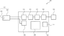
図20は、本発明に係る生体情報測定装置の一実施形態としての血流計801の構成を示す図である。同図に示すように、本実施形態の血流計は、光学センサ201、前置増幅器202、駆動/演算装置203、求めた血流等を表示する出力部204を有する。なお、以下において図1から図19に使用された符号も利用して説明する。
FIG. 20 is a diagram showing a configuration of a
光学センサ201は外部の被検体に光を当て、被検体内で散乱した散乱光を受光する。光学センサ201は半導体基板上に集積化されて形成されていてもよく、図1及び図5〜9で説明した光学センサを利用してもよい。
The
前置増幅器202は光学センサ201からの出力を増幅して出力する。図10〜12のセンサチップで説明したように、光学センサ201を前置増幅器202の基板上に搭載することもできる。光学センサ201及び前置増幅器202とあわせて一体としたセンサチップ620とすることで、人体等に容易に装着できる形状に構成することが可能である。前置増幅器202は信号調節回路210と接続されており、図10〜12で説明したように、増幅回路95で増幅された受光素子17からの信号を受信する。
The
駆動/演算装置203は、A/D変換器205、発光素子駆動回路206、デジタル信号プロセッサ(DSP)207、電源供給部208、インターフェース209、信号調節回路210及び表示部211を含み、小型液晶ディスプレイ等の出力部204に接続される。駆動/演算装置203は、全体をLSIとして構成することが可能である。駆動/演算装置203は発光素子(LD)を駆動させ、散乱光を解析することにより血流を求める。
The drive /
発光素子駆動回路206は前置増幅器202に接続され、前置増幅器202を通じて光学センサ201へ電力を供給する。すなわち、図1及び図5〜9で説明した光学センサの発光素子15は発光素子駆動回路206の指示によって光の照射及び消燈を行う。
The light emitting
A/D変換器205は、入力されたアナログ信号を所定の周波数でサンプリングを行い、量子化して出力する。被検体の血流等を測定する場合のサンプリング周波数は200kHzであることが例示できる。
The A /
DSP207は、入力されたデジタル信号を所定の規則に従い処理を行う電気回路である。DSP207は大量のデジタル信号のデータを高速に処理できるため、入力されたデジタル信号を処理した結果をリアルタイムで出力することができる。DSP207はA/D変換器205からの信号から血流等の生体情報を求めるための演算を行う。
The
インターフェース209は、駆動/演算装置203と外部の周辺機器とが通信できるように入力された信号を所定の規格の信号に変換する電気回路である。例えば、インターフェース209は入力された信号をRS−232C規格の信号に変換することが例示できる。
The
電源供給部208は、所定の電圧の電源を外部に供給する電気回路である。交流を直流に変換する回路、電圧変換回路、電圧安定化回路が含まれる。また、電源供給部208はバッテリーであっても良い。電源供給部208は図示しない電気線を通じてA/D変換器205、発光素子駆動回路206、DSP207、インターフェース209、信号調節回路210及び表示部211に電源を供給する。
The
出力部204はインターフェース209から出力されるデータを表示する。小型液晶ディスプレイ等が例示できる。
The
血流計801は以下のように被検体の血流等の生体情報を測定する。センサチップである光学センサ201及び前置増幅器202を血流等の測定箇所である被検体に近接又は接触させる。
The
前記センサチップは次のように被検体に光を照射して被検体からの散乱光を受光する。発光素子15は発光素子駆動回路206から電流が注入され照射光を出射する。発光素子15からの照射光はキャップ13の第一孔19aで血流の測定に必要な径に絞られ、被検体に照射される。第一孔19aから出射した光は被検体内で散乱し、散乱光が光学センサ201へ到達する。前記散乱光はキャップ13の第二孔19bで測定に必要な光のみとなり受光素子17に受光される。
The sensor chip irradiates the subject with light and receives scattered light from the subject as follows. The
受光素子17は前記散乱光を光電変換して散乱光強度信号として出力する。さらに前記散乱光強度信号を受信した前置増幅器202は増幅してアナログ信号を出力する。信号調節回路210は前記アナログ信号から干渉成分の周波数を含む特定の周波数範囲を抽出する。A/D変換器205は信号調節回路210からの信号をアナログ−デジタル変換してデジタル信号を出力する。
The
DSP17は前記デジタル信号の信号処理を行い、前記散乱光の干渉成分の周波数解析を行う。具体的には、散乱光Sの干渉成分の周波数が血流速度に相当し、散乱光Sの強度は移動している血液量に相当しており、血流速度と血液量との積で血流量が求められる。さらに、散乱信号波形には、脈拍による変調成分もあり、脈拍の検出も可能である。DSP207は前記周波数解析の結果である被検体の情報を被検体情報信号として出力する。
The
表示部211はDSP207からの被検体情報信号を表示する。また、インターフェース209は前記被検体情報信号をRS−232C規格の信号に変換して表示部204に出力する。以上の説明ように、血流計801は被検体の血流等の生体情報を測定する。
The
本発明に係る血流計の測定結果を図21に示して説明する。図21(a)のグラフは血流計801により測定された血流量の時間的な推移のデータであり、図21(b)のグラフは市販の標準的な血流計(市販血流計)により同時に測定されたデータである。市販血流計の測定方法は血流計801の測定方法(ドップラーシフト法)と同様である。
The measurement result of the blood flow meter according to the present invention will be described with reference to FIG. The graph of FIG. 21A is data of the temporal transition of the blood flow measured by the
いずれの血流計も測定方法は、指に本装置を当て、手首を強く締めることによって阻血し、徐々に開放し、最後に完全に開放した場合の血流量を示している。血流計801の測定結果は、市販血流計の測定結果と比べて増幅回路の応答特性の違いにより脈波形状が平均化されているが、血流量自体の増減傾向は一致している。
Each blood flow meter shows the blood flow rate when the device is applied to a finger, the blood is blocked by tightening the wrist strongly, gradually opened, and finally completely opened. In the measurement result of the
市販血流計は、発光素子からの光を光ファイバに結合して前記光ファイバから出力する光を被検体に照射している。さらに、市販血流計は、被検体で散乱した散乱光を他の光ファイバで受光して受光素子に結合している。光ファイバは曲がりかたの変化や測定中の振動等で光の伝搬モードが変化するため、市販血流計で生体情報を測定する場合、被検体の動作を制限する必要があった。血流計801は光ファイバを使用しないため、被検体の動作を制限することなく正確な生体情報を測定することができる。
The commercially available blood flow meter couples light from a light emitting element to an optical fiber and irradiates a subject with light output from the optical fiber. Furthermore, the commercially available blood flow meter receives scattered light scattered by the subject with another optical fiber and couples it to the light receiving element. Since the optical fiber changes its light propagation mode due to changes in bending, vibration during measurement, and the like, it is necessary to limit the operation of the subject when measuring biological information with a commercially available blood flow meter. Since the
さらに、血流計801は、図1及び図5〜9で説明した光学センサを利用しているため、高精度に生体情報を測定でき、製造コストを低くすることができる。
Furthermore, since the
実施の形態1〜3では、発光素子として面発光型の半導体レーザを使用し、受光素子として面入射型のフォトダイオードを使用した光学センサ及びセンサチップ及び生体情報測定装置を説明した。発光素子は端面発光型でもよく、受光素子は端面入射型でもかまわない。以下に端面発光型の発光素子及び端面入射型の受光素子を使用した実施例を説明する。 In the first to third embodiments, the optical sensor, the sensor chip, and the biological information measuring apparatus using the surface emitting semiconductor laser as the light emitting element and using the surface incident type photodiode as the light receiving element have been described. The light emitting element may be an end face light emitting type, and the light receiving element may be an end face incident type. An embodiment using an edge-emitting light emitting element and an edge-incident light receiving element will be described below.
(実施の形態4)
本実施形態の光学センサの前記発光素子は、前記絶縁基板の面と水平な方向に出射光を端面から出射する端面発光型であり、前記受光素子は、前記絶縁基板の面と水平な方向からの散乱光を端面で受光する端面入射型であり、前記キャップの前記第一開口部は、前記発光素子に対して前記発光素子の出射光の出射方向にあり、前記キャップの前記第二開口部は、前記受光素子に対して前記受光素子が散乱光を受光できる方向にあることを特徴とする。
(Embodiment 4)
The light emitting element of the optical sensor of the present embodiment is an end surface light emitting type that emits outgoing light from the end face in a direction parallel to the surface of the insulating substrate, and the light receiving element is from a direction horizontal to the surface of the insulating substrate. The first opening of the cap is in the emission direction of the emitted light of the light emitting element with respect to the light emitting element, and the second opening of the cap Is characterized in that the light receiving element is in a direction capable of receiving scattered light with respect to the light receiving element.
図24は、端面発光型の発光素子及び端面入射型の受光素子を使用した光学センサ524の概略図である。図24(a)は光学センサ524をキャップ13側から見た上面図であり、図24(b)は光学センサ524の開口部側から見た側面図である。図26及び図27においても同様である。
FIG. 24 is a schematic diagram of an
発光素子245は端面発光型の半導体レーザである。発光素子245は絶縁基板11の面に対して水平な方向へ出射光Lを出射できるように絶縁基板11に搭載される。受光素子247は端面入射型のフォトダイオードである。受光素子247は絶縁基板11の面に対して水平な方向からの散乱光Sを受光できるように搭載される。ここで、散乱光Sは出射光Lが外部の被検体で散乱した光である。従って、受光素子247は散乱光Sを感度良く受光できる向きで搭載される。図24では、出射光Lと散乱光Sの光軸は平行として示している。
The
キャップ13は第一開口部249a及び第二開口部249bを側面に有する。発光素子245は、第一開口部249aを通じて出射光Lを出射する。受光素子247は、第二開口部249bを通じて散乱光Sを受光する。第一開口部249aと第二開口部249bとは並列して配置される。
The
図25は、光学センサ524の絶縁基板11上に形成される電気配線を示したものである。それぞれの電気配線と発光素子245及び受光素子247との接続は図4の説明と同様である。
FIG. 25 shows electrical wiring formed on the insulating
光学センサ524は、図1の光学センサ501の説明と同様に低コストで製造でき、高精度に被検体の生体情報を測定することができる。
The
(実施の形態5)
本実施形態の光学センサの前記発光素子は、前記絶縁基板の法線方向に出射光を出射する面発光型であり、前記受光素子は、前記絶縁基板の面と水平な方向からの散乱光を端面で受光する端面入射型であり、前記キャップは、前記発光素子の出射光の方向を前記絶縁基板の面と水平な方向へ変換する光路変換素子をさらに有しており、前記キャップの前記第一開口部は、前記発光素子の出射光が前記キャップの前記光路変換素子で変換された光路方向にあり、前記キャップの前記第二開口部は、前記受光素子に対して前記受光素子が散乱光を受光できる方向にあることを特徴とする。
(Embodiment 5)
The light emitting element of the optical sensor of this embodiment is a surface-emitting type that emits outgoing light in the normal direction of the insulating substrate, and the light receiving element emits scattered light from a direction parallel to the surface of the insulating substrate. The cap is of an end surface incident type that receives light at an end surface, and the cap further includes an optical path conversion element that converts a direction of emitted light of the light emitting element into a direction parallel to a surface of the insulating substrate, The one opening is in an optical path direction in which the light emitted from the light emitting element is converted by the optical path conversion element of the cap, and the second opening of the cap has the light receiving element scattered light with respect to the light receiving element. It is in the direction which can receive light.
図26は、面発光型の発光素子及び端面入射型の受光素子を使用した光学センサ526の概略図である。光学センサ526と図24の光学センサ524との違いは、発光素子が端面発光型ではなく面発光型を使用している点である。また、発光素子15は上方に向けて出射光Lを出射するため、キャップ13は第一開口部249aへ向けて光路を変換する光路変換素子262を有する。光路変換素子262は例えば鏡である。図26(c)は図26(a)のD−D’で切断した断面図である。
FIG. 26 is a schematic diagram of an
光路変換素子262は、発光素子15から上方へ照射された出射光Lを第一開口部249aへ変換する。従って、光学センサ526は図24で説明した光学センサ524と同様の効果を得ることができる。
The optical
(実施の形態6)
本実施形態の光学センサの前記発光素子は、前記絶縁基板の面と水平な方向に出射光を端面から出射する端面発光型であり、前記受光素子は、前記絶縁基板の法線方向からの散乱光を受光する面入射型であり、前記キャップは、前記絶縁基板の面と水平な方向である散乱光の方向を前記絶縁基板の法線方向へ変換する光路変換素子をさらに有しており、前記キャップの前記第一開口部は、前記発光素子に対して前記発光素子の出射光の出射方向にあり、前記キャップの前記第二開口部は、前記キャップの前記光路変換素子に対して前記キャップの前記光路変換素子に散乱光を照射できる方向にあり、前記キャップの光路変換素子は、前記第二開口部を通過した散乱光の光路を変換して前記受光素子に受光させることを特徴とする。
(Embodiment 6)
The light emitting element of the optical sensor of the present embodiment is an end surface light emitting type that emits outgoing light from the end face in a direction parallel to the surface of the insulating substrate, and the light receiving element is scattered from the normal direction of the insulating substrate. It is a surface incidence type that receives light, and the cap further includes an optical path conversion element that converts the direction of scattered light, which is a direction parallel to the surface of the insulating substrate, into the normal direction of the insulating substrate The first opening of the cap is in an emission direction of emitted light of the light emitting element with respect to the light emitting element, and the second opening of the cap is with respect to the optical path conversion element of the cap. The optical path conversion element of the cap is in a direction in which scattered light can be irradiated, and the optical path conversion element of the cap converts the optical path of the scattered light that has passed through the second opening and causes the light receiving element to receive the light. .
図27は、端面発光型の発光素子及び面入射型の受光素子を使用した光学センサ527の概略図である。光学センサ527と図24の光学センサ524との違いは、受光素子が端面入射型ではなく面入射型を使用している点である。また、受光素子17は上方からの散乱光Sを出射するため、キャップ13は第二開口部249bから入射する散乱光Sを受光素子17の受光面へ向けて光路を変換する光路変換素子272を有する。光路変換素子272は例えば鏡である。図27(c)は図27(a)のD−D’で切断した断面図である。
FIG. 27 is a schematic diagram of an
光路変換素子272は、絶縁基板11の面に水平に第二開口部249bから入射する散乱光Sを、受光素子17が受光面で受光できるように散乱光Sの光軸を変換する。従って、光学センサ527は図24で説明した光学センサ524と同様の効果を得ることができる。
The optical
(実施の形態7)
図24、図26又は図27で説明した光学センサを増幅器が搭載された回路基板に搭載してセンサチップとすることができる。
(Embodiment 7)
The optical sensor described in FIG. 24, FIG. 26 or FIG. 27 can be mounted on a circuit board on which an amplifier is mounted to form a sensor chip.
本実施形態のセンサチップは、図24、図26又は図27に記載の光学センサと、長手方向の一端に前記光学センサを搭載する短冊形の回路基板と、を備えるセンサチップであって、前記光学センサは、前記発光素子の出射光を前記回路基板の他端から一端の方向へ出射することを特徴とする。 The sensor chip of the present embodiment is a sensor chip comprising the optical sensor described in FIG. 24, FIG. 26 or FIG. 27 and a strip-shaped circuit board on which the optical sensor is mounted at one end in the longitudinal direction. The optical sensor emits light emitted from the light emitting element in the direction from the other end to the one end of the circuit board.
図28にセンサチップ628を示す。センサチップ628は、図24の光学センサ524を短冊形の回路基板491の一端に搭載する。また、第一開口部249a及び第二開口部249bが回路基板491の他端側と反対側を向くように光学センサ524は回路基板491に搭載される。センサチップ628は、図示しない電源回路や増幅器も搭載している。センサチップ628は、図20の血流計801のセンサチップ620の代替とすることができる。
FIG. 28 shows the
生体情報測定の際、センサチップ628の一端を被検体900に近づける。図24で説明した発光素子245から出射光Lを出射することで、センサチップ628の光学センサ524は、発光素子245の出射光Lを回路基板491の他端から一端の方向へ出射し、回路基板491の一端の先にある被検体900へ照射する。また、センサチップ628の光学センサ524は、被検体900の内部で出射光Lが散乱した散乱光Sを図24で説明した第二開口部249bを通じて図24で説明した受光素子247で受光する。血流計801は、センサチップ628を利用しても図20で説明したように生体情報である血流を測定できる。
When measuring biological information, one end of the
さらに、センサチップ628は、短冊形の回路基板491の先端に光学センサ524を搭載するため、被検体900が奥にある場合や、狭い箇所にある場合にも生体情報を測定することができる。例えば、センサチップ628は、被検体900が鼻の奥、口腔内又は腸内の血流を測定することができる。
Furthermore, since the
また、図29のセンサチップ629のように、光学センサ524を回路基板491に搭載してもよい。具体的には、センサチップ629は、光学センサ524と、長手方向の一端に光学センサ524を搭載する短冊形の回路基板491と、を備えるセンサチップであって、光学センサ524は、図24で説明した発光素子245の出射光Lを回路基板491の面と平行であり、且つ回路基板491の長手方向と直交する方向へ出射することを特徴とする。センサチップ629は、図28のセンサチップ628と同様の構成であり、同様の効果を得ることができる。
Further, an
なお、センサチップ628及びセンサチップ629において、回路基板491に搭載する光学センサは、図24の光学センサ524の他に図26の光学センサ526又は図27の光学センサ527でもよい。
In the
本発明の生体情報測定装置及び光学センサは、健康保持や健康診断のための健康器具に適用することができる。また、被検体としては人間に限らず動物や植物でもよい。さらに、フッ素樹脂チューブ、シリコンチューブ等、発光素子からの光が透過できる管であれば、内部を流れる液体の流量を測定することができるため、本発明の生体情報測定装置及び光学センサは半導体製造装置や冷却装置の流量計に使用することができる。 The biological information measuring apparatus and optical sensor of the present invention can be applied to health appliances for health maintenance and health diagnosis. Further, the subject is not limited to a human but may be an animal or a plant. Furthermore, since the flow rate of the liquid flowing inside the tube can be measured as long as the tube can transmit light from the light emitting element, such as a fluororesin tube and a silicon tube, the biological information measuring device and the optical sensor of the present invention are manufactured by a semiconductor It can be used for flowmeters of equipment and cooling devices.
501、505〜509、524、526、527 光学センサ
610〜612、620、628、629 センサチップ
801 血流計
11 絶縁基板
13 キャップ
15、245 発光素子
17、247 受光素子
19a 第一孔
249a 第一開口部
249b 第二開口部
19b 第二孔
21a〜e 電気配線
23 ワイヤ
25 絶縁膜
75 仕切り板
81a〜d 電気配線
83 ワイヤ
87a、b ワイヤ
88a、b ワイヤ
85 増幅回路
91 プリント回路基板
93a〜d 電極パッド
95 増幅回路
95a、b オペアンプ
97 ワイヤ
99 電気配線
121 孔
123 突起
201 光学センサ
202 前置増幅器
203 駆動/演算装置
204 出力部
205 A/D変換器
206 発光素子駆動回路
207 DSP
208 電源供給部
209 インターフェース
210 信号調節回路
211 表示部
262、272 光路変換素子
321 シリコン基板
322、324 電極
361 レーザダイオード
325 フォトダイオード
326 カバー基板
362 屈折レンズ
327 331 遮光膜
329 ワイヤ
491 回路基板
L 出射光
S 散乱光
501, 505-509, 524, 526, 527 Optical sensor 610-612, 620, 628, 629
208
Claims (3)
外部からの散乱光を受光する受光素子と、
前記発光素子及び前記受光素子を表面に搭載する絶縁基板と、
前記絶縁基板上で前記発光素子及び前記受光素子を覆う不透明なキャップと、
を備える光学センサであって、
前記キャップは、前記発光素子からの出射光の一部を前記光学センサの外部へ通過させる第一開口部及び前記発光素子からの光が前記光学センサの外部で散乱した散乱光の一部を通過させて前記受光素子に受光させる第二開口部を有し、
前記発光素子は、前記絶縁基板の法線方向に出射光を出射する面発光型であり、
前記受光素子は、前記絶縁基板の面と水平な方向からの散乱光を端面で受光する端面入射型であり、
前記キャップは、前記発光素子の出射光の方向を前記絶縁基板の面と水平な方向へ変換する光路変換素子をさらに有しており、
前記キャップの前記第一開口部は、前記発光素子の出射光が前記キャップの前記光路変換素子で変換された光路方向にあり、
前記キャップの前記第二開口部は、前記受光素子に対して前記受光素子が散乱光を受光できる方向にあることを特徴とする光学センサ。 A light emitting element for generating outgoing light;
A light receiving element for receiving scattered light from the outside;
An insulating substrate on which the light emitting element and the light receiving element are mounted;
An opaque cap that covers the light emitting element and the light receiving element on the insulating substrate;
An optical sensor comprising:
The cap passes through a first opening that allows a part of the light emitted from the light emitting element to pass outside the optical sensor and a part of the scattered light that is scattered from outside the optical sensor. A second opening for allowing the light receiving element to receive light,
The light-emitting element is a surface-emitting type that emits outgoing light in a normal direction of the insulating substrate,
The light receiving element is an end face incident type that receives scattered light from a direction parallel to the surface of the insulating substrate at an end face;
The cap further includes an optical path conversion element that converts the direction of the emitted light of the light emitting element into a direction horizontal to the surface of the insulating substrate;
The first opening of the cap is in an optical path direction in which emitted light of the light emitting element is converted by the optical path conversion element of the cap,
The optical sensor, wherein the second opening of the cap is in a direction in which the light receiving element can receive scattered light with respect to the light receiving element.
長手方向の一端に前記光学センサを搭載する短冊形の回路基板と、
を備えるセンサチップであって、
前記光学センサは、前記発光素子の出射光を前記回路基板の他端から一端の方向へ出射することを特徴とするセンサチップ。 The optical sensor of claim 1;
A strip-shaped circuit board on which the optical sensor is mounted at one end in the longitudinal direction;
A sensor chip comprising:
The optical sensor emits light emitted from the light emitting element in the direction from the other end to the one end of the circuit board.
長手方向の一端に前記光学センサを搭載する短冊形の回路基板と、
を備えるセンサチップであって、
前記光学センサは、前記発光素子の出射光を前記回路基板の面と平行であり、且つ前記回路基板の長手方向と直交する方向へ出射することを特徴とするセンサチップ。 The optical sensor of claim 1;
A strip-shaped circuit board on which the optical sensor is mounted at one end in the longitudinal direction;
A sensor chip comprising:
The optical sensor emits light emitted from the light emitting element in a direction parallel to the surface of the circuit board and perpendicular to the longitudinal direction of the circuit board.
Priority Applications (1)
| Application Number | Priority Date | Filing Date | Title |
|---|---|---|---|
| JP2011163180A JP5301618B2 (en) | 2006-06-01 | 2011-07-26 | Optical sensor and sensor chip |
Applications Claiming Priority (3)
| Application Number | Priority Date | Filing Date | Title |
|---|---|---|---|
| JP2006153170 | 2006-06-01 | ||
| JP2006153170 | 2006-06-01 | ||
| JP2011163180A JP5301618B2 (en) | 2006-06-01 | 2011-07-26 | Optical sensor and sensor chip |
Related Parent Applications (1)
| Application Number | Title | Priority Date | Filing Date |
|---|---|---|---|
| JP2007116089A Division JP2008010832A (en) | 2006-06-01 | 2007-04-25 | Optical sensor, sensor chip, and biological information measuring device |
Publications (2)
| Publication Number | Publication Date |
|---|---|
| JP2012021993A JP2012021993A (en) | 2012-02-02 |
| JP5301618B2 true JP5301618B2 (en) | 2013-09-25 |
Family
ID=45776356
Family Applications (1)
| Application Number | Title | Priority Date | Filing Date |
|---|---|---|---|
| JP2011163180A Active JP5301618B2 (en) | 2006-06-01 | 2011-07-26 | Optical sensor and sensor chip |
Country Status (1)
| Country | Link |
|---|---|
| JP (1) | JP5301618B2 (en) |
Cited By (1)
| Publication number | Priority date | Publication date | Assignee | Title |
|---|---|---|---|---|
| KR20190009954A (en) * | 2017-07-20 | 2019-01-30 | 엘지이노텍 주식회사 | Sensor package |
Families Citing this family (2)
| Publication number | Priority date | Publication date | Assignee | Title |
|---|---|---|---|---|
| US8921759B2 (en) * | 2012-07-26 | 2014-12-30 | Optiz, Inc. | Integrated image sensor package with liquid crystal lens |
| JP6666359B2 (en) * | 2015-11-30 | 2020-03-13 | 新日本無線株式会社 | Photo sensor |
Family Cites Families (2)
| Publication number | Priority date | Publication date | Assignee | Title |
|---|---|---|---|---|
| JP3882756B2 (en) * | 2003-01-30 | 2007-02-21 | 日本電信電話株式会社 | Blood flow sensor and blood flow meter |
| JP4061409B2 (en) * | 2004-11-09 | 2008-03-19 | 国立大学法人九州大学 | Sensor unit and biosensor |
-
2011
- 2011-07-26 JP JP2011163180A patent/JP5301618B2/en active Active
Cited By (2)
| Publication number | Priority date | Publication date | Assignee | Title |
|---|---|---|---|---|
| KR20190009954A (en) * | 2017-07-20 | 2019-01-30 | 엘지이노텍 주식회사 | Sensor package |
| KR102510605B1 (en) | 2017-07-20 | 2023-03-16 | 쑤저우 레킨 세미컨덕터 컴퍼니 리미티드 | Sensor package |
Also Published As
| Publication number | Publication date |
|---|---|
| JP2012021993A (en) | 2012-02-02 |
Similar Documents
| Publication | Publication Date | Title |
|---|---|---|
| JP4061409B2 (en) | Sensor unit and biosensor | |
| JP4724559B2 (en) | Optical sensor and sensor unit thereof | |
| JP2008010832A (en) | Optical sensor, sensor chip, and biological information measuring device | |
| US20110260176A1 (en) | Light-emitting sensor device and method for manufacturing the same | |
| JP3882756B2 (en) | Blood flow sensor and blood flow meter | |
| KR20080100332A (en) | Optical transmission/reception device | |
| Kimura et al. | Integrated laser Doppler blood flowmeter designed to enable wafer-level packaging | |
| JPWO2008065699A1 (en) | Self-luminous sensor device and biological information detection method | |
| JP3651442B2 (en) | Blood flow meter and blood flow sensor | |
| JP2012523858A (en) | Sensing device for characteristics of body tissue | |
| US20150190058A1 (en) | Biological information detector and biological information measuring device | |
| JP4718324B2 (en) | Optical sensor and sensor unit thereof | |
| JP5301618B2 (en) | Optical sensor and sensor chip | |
| JP2010200970A (en) | Optical sensor and method for manufacturing the same | |
| JP4460566B2 (en) | Optical sensor and biological information measuring device | |
| JP5031896B2 (en) | Self-luminous sensor device | |
| JP2008272085A (en) | Blood-flow sensor | |
| US7128716B2 (en) | Blood flowmeter and sensor part of the blood flowmeter | |
| US20230243680A1 (en) | Measurement module and measurement device | |
| JP4600555B2 (en) | Measuring device | |
| Kimura et al. | Low-power consumption integrated laser Doppler blood flowmeter with a built-in silicon microlens | |
| US11033193B2 (en) | Light emitting device, biological information measuring apparatus, and method of manufacturing light emitting device | |
| JP2008278983A (en) | Sensor head | |
| JP4714017B2 (en) | Biosensor | |
| JP4668234B2 (en) | Blood flow measuring device |
Legal Events
| Date | Code | Title | Description |
|---|---|---|---|
| TRDD | Decision of grant or rejection written | ||
| A01 | Written decision to grant a patent or to grant a registration (utility model) |
Free format text: JAPANESE INTERMEDIATE CODE: A01 Effective date: 20130618 |
|
| A61 | First payment of annual fees (during grant procedure) |
Free format text: JAPANESE INTERMEDIATE CODE: A61 Effective date: 20130619 |
|
| R150 | Certificate of patent or registration of utility model |
Ref document number: 5301618 Country of ref document: JP Free format text: JAPANESE INTERMEDIATE CODE: R150 Free format text: JAPANESE INTERMEDIATE CODE: R150 |
|
| S531 | Written request for registration of change of domicile |
Free format text: JAPANESE INTERMEDIATE CODE: R313531 |
|
| R350 | Written notification of registration of transfer |
Free format text: JAPANESE INTERMEDIATE CODE: R350 |