JP5286034B2 - Method for manufacturing semiconductor device - Google Patents
Method for manufacturing semiconductor device Download PDFInfo
- Publication number
- JP5286034B2 JP5286034B2 JP2008284435A JP2008284435A JP5286034B2 JP 5286034 B2 JP5286034 B2 JP 5286034B2 JP 2008284435 A JP2008284435 A JP 2008284435A JP 2008284435 A JP2008284435 A JP 2008284435A JP 5286034 B2 JP5286034 B2 JP 5286034B2
- Authority
- JP
- Japan
- Prior art keywords
- film
- semiconductor layer
- insulating film
- semiconductor
- semiconductor film
- Prior art date
- Legal status (The legal status is an assumption and is not a legal conclusion. Google has not performed a legal analysis and makes no representation as to the accuracy of the status listed.)
- Expired - Fee Related
Links
- 239000004065 semiconductor Substances 0.000 title claims description 534
- 238000000034 method Methods 0.000 title claims description 51
- 238000004519 manufacturing process Methods 0.000 title claims description 50
- 238000010438 heat treatment Methods 0.000 claims description 112
- 239000012535 impurity Substances 0.000 claims description 95
- IJGRMHOSHXDMSA-UHFFFAOYSA-N Atomic nitrogen Chemical compound N#N IJGRMHOSHXDMSA-UHFFFAOYSA-N 0.000 claims description 90
- 229910052760 oxygen Inorganic materials 0.000 claims description 61
- 239000001301 oxygen Substances 0.000 claims description 61
- QVGXLLKOCUKJST-UHFFFAOYSA-N atomic oxygen Chemical compound [O] QVGXLLKOCUKJST-UHFFFAOYSA-N 0.000 claims description 60
- 150000004767 nitrides Chemical class 0.000 claims description 53
- 229910052757 nitrogen Inorganic materials 0.000 claims description 45
- 238000005530 etching Methods 0.000 claims description 21
- 238000005121 nitriding Methods 0.000 claims description 16
- 230000001590 oxidative effect Effects 0.000 claims description 15
- 239000004020 conductor Substances 0.000 claims description 2
- 239000010408 film Substances 0.000 description 767
- 239000010410 layer Substances 0.000 description 208
- 239000000758 substrate Substances 0.000 description 200
- VYPSYNLAJGMNEJ-UHFFFAOYSA-N silicon dioxide Inorganic materials O=[Si]=O VYPSYNLAJGMNEJ-UHFFFAOYSA-N 0.000 description 60
- 229910052814 silicon oxide Inorganic materials 0.000 description 56
- 150000002500 ions Chemical class 0.000 description 47
- 229910052710 silicon Inorganic materials 0.000 description 35
- XUIMIQQOPSSXEZ-UHFFFAOYSA-N Silicon Chemical compound [Si] XUIMIQQOPSSXEZ-UHFFFAOYSA-N 0.000 description 33
- 239000010703 silicon Substances 0.000 description 33
- 229910052581 Si3N4 Inorganic materials 0.000 description 29
- HQVNEWCFYHHQES-UHFFFAOYSA-N silicon nitride Chemical compound N12[Si]34N5[Si]62N3[Si]51N64 HQVNEWCFYHHQES-UHFFFAOYSA-N 0.000 description 29
- 238000000926 separation method Methods 0.000 description 26
- 239000013078 crystal Substances 0.000 description 25
- 229910021417 amorphous silicon Inorganic materials 0.000 description 22
- 230000004888 barrier function Effects 0.000 description 19
- 239000007789 gas Substances 0.000 description 18
- 239000001257 hydrogen Substances 0.000 description 17
- 229910052739 hydrogen Inorganic materials 0.000 description 17
- 239000010409 thin film Substances 0.000 description 16
- 230000015572 biosynthetic process Effects 0.000 description 15
- UFHFLCQGNIYNRP-UHFFFAOYSA-N Hydrogen Chemical compound [H][H] UFHFLCQGNIYNRP-UHFFFAOYSA-N 0.000 description 14
- 239000011521 glass Substances 0.000 description 13
- 125000004429 atom Chemical group 0.000 description 11
- 230000008569 process Effects 0.000 description 11
- 238000001994 activation Methods 0.000 description 10
- 230000004913 activation Effects 0.000 description 10
- 230000006870 function Effects 0.000 description 10
- 238000004151 rapid thermal annealing Methods 0.000 description 10
- 239000000126 substance Substances 0.000 description 10
- CBENFWSGALASAD-UHFFFAOYSA-N Ozone Chemical compound [O-][O+]=O CBENFWSGALASAD-UHFFFAOYSA-N 0.000 description 9
- 238000005468 ion implantation Methods 0.000 description 9
- 229910021421 monocrystalline silicon Inorganic materials 0.000 description 9
- XKRFYHLGVUSROY-UHFFFAOYSA-N Argon Chemical compound [Ar] XKRFYHLGVUSROY-UHFFFAOYSA-N 0.000 description 8
- KRHYYFGTRYWZRS-UHFFFAOYSA-N Fluorane Chemical compound F KRHYYFGTRYWZRS-UHFFFAOYSA-N 0.000 description 8
- 230000001133 acceleration Effects 0.000 description 8
- 239000002585 base Substances 0.000 description 8
- 238000005229 chemical vapour deposition Methods 0.000 description 8
- 238000004891 communication Methods 0.000 description 8
- 229910052732 germanium Inorganic materials 0.000 description 8
- GNPVGFCGXDBREM-UHFFFAOYSA-N germanium atom Chemical compound [Ge] GNPVGFCGXDBREM-UHFFFAOYSA-N 0.000 description 8
- 238000009792 diffusion process Methods 0.000 description 7
- MWUXSHHQAYIFBG-UHFFFAOYSA-N Nitric oxide Chemical compound O=[N] MWUXSHHQAYIFBG-UHFFFAOYSA-N 0.000 description 6
- 238000006243 chemical reaction Methods 0.000 description 6
- 238000000151 deposition Methods 0.000 description 6
- 238000010884 ion-beam technique Methods 0.000 description 6
- 239000000463 material Substances 0.000 description 6
- 238000012545 processing Methods 0.000 description 6
- 238000003860 storage Methods 0.000 description 6
- 230000007547 defect Effects 0.000 description 5
- 230000008021 deposition Effects 0.000 description 5
- 239000011261 inert gas Substances 0.000 description 5
- 238000002156 mixing Methods 0.000 description 5
- 230000003647 oxidation Effects 0.000 description 5
- 238000007254 oxidation reaction Methods 0.000 description 5
- 230000005855 radiation Effects 0.000 description 5
- 238000007725 thermal activation Methods 0.000 description 5
- XLYOFNOQVPJJNP-UHFFFAOYSA-N water Substances O XLYOFNOQVPJJNP-UHFFFAOYSA-N 0.000 description 5
- ZOXJGFHDIHLPTG-UHFFFAOYSA-N Boron Chemical compound [B] ZOXJGFHDIHLPTG-UHFFFAOYSA-N 0.000 description 4
- GQPLMRYTRLFLPF-UHFFFAOYSA-N Nitrous Oxide Chemical compound [O-][N+]#N GQPLMRYTRLFLPF-UHFFFAOYSA-N 0.000 description 4
- OAICVXFJPJFONN-UHFFFAOYSA-N Phosphorus Chemical compound [P] OAICVXFJPJFONN-UHFFFAOYSA-N 0.000 description 4
- 238000004833 X-ray photoelectron spectroscopy Methods 0.000 description 4
- 238000000137 annealing Methods 0.000 description 4
- 229910052786 argon Inorganic materials 0.000 description 4
- 229910052785 arsenic Inorganic materials 0.000 description 4
- RQNWIZPPADIBDY-UHFFFAOYSA-N arsenic atom Chemical compound [As] RQNWIZPPADIBDY-UHFFFAOYSA-N 0.000 description 4
- 229910052796 boron Inorganic materials 0.000 description 4
- 239000000470 constituent Substances 0.000 description 4
- 230000005684 electric field Effects 0.000 description 4
- 239000001307 helium Substances 0.000 description 4
- 229910052734 helium Inorganic materials 0.000 description 4
- SWQJXJOGLNCZEY-UHFFFAOYSA-N helium atom Chemical compound [He] SWQJXJOGLNCZEY-UHFFFAOYSA-N 0.000 description 4
- 229910052698 phosphorus Inorganic materials 0.000 description 4
- 239000011574 phosphorus Substances 0.000 description 4
- 230000001681 protective effect Effects 0.000 description 4
- 239000010453 quartz Substances 0.000 description 4
- WGTYBPLFGIVFAS-UHFFFAOYSA-M tetramethylammonium hydroxide Chemical compound [OH-].C[N+](C)(C)C WGTYBPLFGIVFAS-UHFFFAOYSA-M 0.000 description 4
- 238000001039 wet etching Methods 0.000 description 4
- KWYUFKZDYYNOTN-UHFFFAOYSA-M Potassium hydroxide Chemical compound [OH-].[K+] KWYUFKZDYYNOTN-UHFFFAOYSA-M 0.000 description 3
- BLRPTPMANUNPDV-UHFFFAOYSA-N Silane Chemical compound [SiH4] BLRPTPMANUNPDV-UHFFFAOYSA-N 0.000 description 3
- BOTDANWDWHJENH-UHFFFAOYSA-N Tetraethyl orthosilicate Chemical compound CCO[Si](OCC)(OCC)OCC BOTDANWDWHJENH-UHFFFAOYSA-N 0.000 description 3
- 229910052783 alkali metal Inorganic materials 0.000 description 3
- 150000001340 alkali metals Chemical class 0.000 description 3
- 229910052784 alkaline earth metal Inorganic materials 0.000 description 3
- 150000001342 alkaline earth metals Chemical class 0.000 description 3
- 230000000694 effects Effects 0.000 description 3
- JEGUKCSWCFPDGT-UHFFFAOYSA-N h2o hydrate Chemical compound O.O JEGUKCSWCFPDGT-UHFFFAOYSA-N 0.000 description 3
- -1 hydrogen ions Chemical class 0.000 description 3
- QOSATHPSBFQAML-UHFFFAOYSA-N hydrogen peroxide;hydrate Chemical compound O.OO QOSATHPSBFQAML-UHFFFAOYSA-N 0.000 description 3
- 230000005660 hydrophilic surface Effects 0.000 description 3
- 230000001771 impaired effect Effects 0.000 description 3
- 229910021426 porous silicon Inorganic materials 0.000 description 3
- SBEQWOXEGHQIMW-UHFFFAOYSA-N silicon Chemical compound [Si].[Si] SBEQWOXEGHQIMW-UHFFFAOYSA-N 0.000 description 3
- LIVNPJMFVYWSIS-UHFFFAOYSA-N silicon monoxide Chemical compound [Si-]#[O+] LIVNPJMFVYWSIS-UHFFFAOYSA-N 0.000 description 3
- WZJUBBHODHNQPW-UHFFFAOYSA-N 2,4,6,8-tetramethyl-1,3,5,7,2$l^{3},4$l^{3},6$l^{3},8$l^{3}-tetraoxatetrasilocane Chemical compound C[Si]1O[Si](C)O[Si](C)O[Si](C)O1 WZJUBBHODHNQPW-UHFFFAOYSA-N 0.000 description 2
- DGAQECJNVWCQMB-PUAWFVPOSA-M Ilexoside XXIX Chemical compound C[C@@H]1CC[C@@]2(CC[C@@]3(C(=CC[C@H]4[C@]3(CC[C@@H]5[C@@]4(CC[C@@H](C5(C)C)OS(=O)(=O)[O-])C)C)[C@@H]2[C@]1(C)O)C)C(=O)O[C@H]6[C@@H]([C@H]([C@@H]([C@H](O6)CO)O)O)O.[Na+] DGAQECJNVWCQMB-PUAWFVPOSA-M 0.000 description 2
- 229910004298 SiO 2 Inorganic materials 0.000 description 2
- 229910000577 Silicon-germanium Inorganic materials 0.000 description 2
- LEVVHYCKPQWKOP-UHFFFAOYSA-N [Si].[Ge] Chemical compound [Si].[Ge] LEVVHYCKPQWKOP-UHFFFAOYSA-N 0.000 description 2
- 239000012670 alkaline solution Substances 0.000 description 2
- 230000000903 blocking effect Effects 0.000 description 2
- 239000011651 chromium Substances 0.000 description 2
- 238000002425 crystallisation Methods 0.000 description 2
- 230000008025 crystallization Effects 0.000 description 2
- 238000010586 diagram Methods 0.000 description 2
- 238000001312 dry etching Methods 0.000 description 2
- 150000002431 hydrogen Chemical class 0.000 description 2
- 239000007943 implant Substances 0.000 description 2
- 238000009413 insulation Methods 0.000 description 2
- 229910052743 krypton Inorganic materials 0.000 description 2
- DNNSSWSSYDEUBZ-UHFFFAOYSA-N krypton atom Chemical compound [Kr] DNNSSWSSYDEUBZ-UHFFFAOYSA-N 0.000 description 2
- 239000011159 matrix material Substances 0.000 description 2
- 239000000203 mixture Substances 0.000 description 2
- 229910052754 neon Inorganic materials 0.000 description 2
- GKAOGPIIYCISHV-UHFFFAOYSA-N neon atom Chemical compound [Ne] GKAOGPIIYCISHV-UHFFFAOYSA-N 0.000 description 2
- 229960001730 nitrous oxide Drugs 0.000 description 2
- 235000013842 nitrous oxide Nutrition 0.000 description 2
- HMMGMWAXVFQUOA-UHFFFAOYSA-N octamethylcyclotetrasiloxane Chemical compound C[Si]1(C)O[Si](C)(C)O[Si](C)(C)O[Si](C)(C)O1 HMMGMWAXVFQUOA-UHFFFAOYSA-N 0.000 description 2
- 239000003960 organic solvent Substances 0.000 description 2
- 150000001282 organosilanes Chemical class 0.000 description 2
- CVLHDNLPWKYNNR-UHFFFAOYSA-N pentasilolane Chemical compound [SiH2]1[SiH2][SiH2][SiH2][SiH2]1 CVLHDNLPWKYNNR-UHFFFAOYSA-N 0.000 description 2
- 229920000548 poly(silane) polymer Polymers 0.000 description 2
- 229910000077 silane Inorganic materials 0.000 description 2
- 229910052708 sodium Inorganic materials 0.000 description 2
- 239000011734 sodium Substances 0.000 description 2
- 239000000243 solution Substances 0.000 description 2
- CZDYPVPMEAXLPK-UHFFFAOYSA-N tetramethylsilane Chemical compound C[Si](C)(C)C CZDYPVPMEAXLPK-UHFFFAOYSA-N 0.000 description 2
- 239000010936 titanium Substances 0.000 description 2
- QGZKDVFQNNGYKY-UHFFFAOYSA-N Ammonia Chemical compound N QGZKDVFQNNGYKY-UHFFFAOYSA-N 0.000 description 1
- JBRZTFJDHDCESZ-UHFFFAOYSA-N AsGa Chemical compound [As]#[Ga] JBRZTFJDHDCESZ-UHFFFAOYSA-N 0.000 description 1
- VYZAMTAEIAYCRO-UHFFFAOYSA-N Chromium Chemical compound [Cr] VYZAMTAEIAYCRO-UHFFFAOYSA-N 0.000 description 1
- YZCKVEUIGOORGS-OUBTZVSYSA-N Deuterium Chemical compound [2H] YZCKVEUIGOORGS-OUBTZVSYSA-N 0.000 description 1
- MYMOFIZGZYHOMD-UHFFFAOYSA-N Dioxygen Chemical compound O=O MYMOFIZGZYHOMD-UHFFFAOYSA-N 0.000 description 1
- 229910001218 Gallium arsenide Inorganic materials 0.000 description 1
- GPXJNWSHGFTCBW-UHFFFAOYSA-N Indium phosphide Chemical compound [In]#P GPXJNWSHGFTCBW-UHFFFAOYSA-N 0.000 description 1
- 238000001237 Raman spectrum Methods 0.000 description 1
- 229910003902 SiCl 4 Inorganic materials 0.000 description 1
- RTAQQCXQSZGOHL-UHFFFAOYSA-N Titanium Chemical compound [Ti] RTAQQCXQSZGOHL-UHFFFAOYSA-N 0.000 description 1
- 238000005411 Van der Waals force Methods 0.000 description 1
- 238000002441 X-ray diffraction Methods 0.000 description 1
- 239000002253 acid Substances 0.000 description 1
- 230000003213 activating effect Effects 0.000 description 1
- 229910052782 aluminium Inorganic materials 0.000 description 1
- XAGFODPZIPBFFR-UHFFFAOYSA-N aluminium Chemical compound [Al] XAGFODPZIPBFFR-UHFFFAOYSA-N 0.000 description 1
- 239000005407 aluminoborosilicate glass Substances 0.000 description 1
- 239000005354 aluminosilicate glass Substances 0.000 description 1
- 238000004458 analytical method Methods 0.000 description 1
- 239000007864 aqueous solution Substances 0.000 description 1
- 229910052788 barium Inorganic materials 0.000 description 1
- DSAJWYNOEDNPEQ-UHFFFAOYSA-N barium atom Chemical compound [Ba] DSAJWYNOEDNPEQ-UHFFFAOYSA-N 0.000 description 1
- 239000005388 borosilicate glass Substances 0.000 description 1
- 239000000919 ceramic Substances 0.000 description 1
- SLLGVCUQYRMELA-UHFFFAOYSA-N chlorosilicon Chemical compound Cl[Si] SLLGVCUQYRMELA-UHFFFAOYSA-N 0.000 description 1
- 229910052804 chromium Inorganic materials 0.000 description 1
- 150000001875 compounds Chemical class 0.000 description 1
- 238000011109 contamination Methods 0.000 description 1
- 229910021419 crystalline silicon Inorganic materials 0.000 description 1
- 238000000354 decomposition reaction Methods 0.000 description 1
- 238000007872 degassing Methods 0.000 description 1
- 229910052805 deuterium Inorganic materials 0.000 description 1
- 238000007865 diluting Methods 0.000 description 1
- 239000012895 dilution Substances 0.000 description 1
- 238000010790 dilution Methods 0.000 description 1
- 229910001873 dinitrogen Inorganic materials 0.000 description 1
- 229910001882 dioxygen Inorganic materials 0.000 description 1
- 238000009826 distribution Methods 0.000 description 1
- 238000005485 electric heating Methods 0.000 description 1
- 230000002349 favourable effect Effects 0.000 description 1
- 235000013305 food Nutrition 0.000 description 1
- 229910052736 halogen Inorganic materials 0.000 description 1
- 150000002367 halogens Chemical class 0.000 description 1
- FFUAGWLWBBFQJT-UHFFFAOYSA-N hexamethyldisilazane Chemical compound C[Si](C)(C)N[Si](C)(C)C FFUAGWLWBBFQJT-UHFFFAOYSA-N 0.000 description 1
- GPRLSGONYQIRFK-UHFFFAOYSA-N hydron Chemical compound [H+] GPRLSGONYQIRFK-UHFFFAOYSA-N 0.000 description 1
- 125000002887 hydroxy group Chemical group [H]O* 0.000 description 1
- 238000007654 immersion Methods 0.000 description 1
- 238000002513 implantation Methods 0.000 description 1
- 239000012212 insulator Substances 0.000 description 1
- 230000001678 irradiating effect Effects 0.000 description 1
- 239000004973 liquid crystal related substance Substances 0.000 description 1
- 238000005259 measurement Methods 0.000 description 1
- 239000012528 membrane Substances 0.000 description 1
- 229910052751 metal Inorganic materials 0.000 description 1
- 239000002184 metal Substances 0.000 description 1
- 238000012986 modification Methods 0.000 description 1
- 230000004048 modification Effects 0.000 description 1
- 230000007935 neutral effect Effects 0.000 description 1
- QJGQUHMNIGDVPM-UHFFFAOYSA-N nitrogen group Chemical group [N] QJGQUHMNIGDVPM-UHFFFAOYSA-N 0.000 description 1
- 238000004806 packaging method and process Methods 0.000 description 1
- 230000035515 penetration Effects 0.000 description 1
- 238000005268 plasma chemical vapour deposition Methods 0.000 description 1
- 238000009832 plasma treatment Methods 0.000 description 1
- 238000005498 polishing Methods 0.000 description 1
- 229910021420 polycrystalline silicon Inorganic materials 0.000 description 1
- 238000003825 pressing Methods 0.000 description 1
- 230000003252 repetitive effect Effects 0.000 description 1
- 239000002210 silicon-based material Substances 0.000 description 1
- 239000002356 single layer Substances 0.000 description 1
- 238000004544 sputter deposition Methods 0.000 description 1
- 230000003746 surface roughness Effects 0.000 description 1
- 238000004381 surface treatment Methods 0.000 description 1
- 229910052715 tantalum Inorganic materials 0.000 description 1
- GUVRBAGPIYLISA-UHFFFAOYSA-N tantalum atom Chemical compound [Ta] GUVRBAGPIYLISA-UHFFFAOYSA-N 0.000 description 1
- MZLGASXMSKOWSE-UHFFFAOYSA-N tantalum nitride Chemical compound [Ta]#N MZLGASXMSKOWSE-UHFFFAOYSA-N 0.000 description 1
- 229910052719 titanium Inorganic materials 0.000 description 1
- QQQSFSZALRVCSZ-UHFFFAOYSA-N triethoxysilane Chemical compound CCO[SiH](OCC)OCC QQQSFSZALRVCSZ-UHFFFAOYSA-N 0.000 description 1
- WFKWXMTUELFFGS-UHFFFAOYSA-N tungsten Chemical compound [W] WFKWXMTUELFFGS-UHFFFAOYSA-N 0.000 description 1
- 229910052721 tungsten Inorganic materials 0.000 description 1
- 239000010937 tungsten Substances 0.000 description 1
Images


Classifications
-
- H—ELECTRICITY
- H01—ELECTRIC ELEMENTS
- H01L—SEMICONDUCTOR DEVICES NOT COVERED BY CLASS H10
- H01L29/00—Semiconductor devices adapted for rectifying, amplifying, oscillating or switching, or capacitors or resistors with at least one potential-jump barrier or surface barrier, e.g. PN junction depletion layer or carrier concentration layer; Details of semiconductor bodies or of electrodes thereof ; Multistep manufacturing processes therefor
- H01L29/66—Types of semiconductor device ; Multistep manufacturing processes therefor
- H01L29/66007—Multistep manufacturing processes
- H01L29/66075—Multistep manufacturing processes of devices having semiconductor bodies comprising group 14 or group 13/15 materials
- H01L29/66227—Multistep manufacturing processes of devices having semiconductor bodies comprising group 14 or group 13/15 materials the devices being controllable only by the electric current supplied or the electric potential applied, to an electrode which does not carry the current to be rectified, amplified or switched, e.g. three-terminal devices
- H01L29/66409—Unipolar field-effect transistors
- H01L29/66477—Unipolar field-effect transistors with an insulated gate, i.e. MISFET
- H01L29/66742—Thin film unipolar transistors
- H01L29/66772—Monocristalline silicon transistors on insulating substrates, e.g. quartz substrates
-
- H—ELECTRICITY
- H01—ELECTRIC ELEMENTS
- H01L—SEMICONDUCTOR DEVICES NOT COVERED BY CLASS H10
- H01L29/00—Semiconductor devices adapted for rectifying, amplifying, oscillating or switching, or capacitors or resistors with at least one potential-jump barrier or surface barrier, e.g. PN junction depletion layer or carrier concentration layer; Details of semiconductor bodies or of electrodes thereof ; Multistep manufacturing processes therefor
- H01L29/40—Electrodes ; Multistep manufacturing processes therefor
- H01L29/41—Electrodes ; Multistep manufacturing processes therefor characterised by their shape, relative sizes or dispositions
- H01L29/417—Electrodes ; Multistep manufacturing processes therefor characterised by their shape, relative sizes or dispositions carrying the current to be rectified, amplified or switched
- H01L29/41725—Source or drain electrodes for field effect devices
- H01L29/41775—Source or drain electrodes for field effect devices characterised by the proximity or the relative position of the source or drain electrode and the gate electrode, e.g. the source or drain electrode separated from the gate electrode by side-walls or spreading around or above the gate electrode
- H01L29/41783—Raised source or drain electrodes self aligned with the gate
-
- H—ELECTRICITY
- H01—ELECTRIC ELEMENTS
- H01L—SEMICONDUCTOR DEVICES NOT COVERED BY CLASS H10
- H01L29/00—Semiconductor devices adapted for rectifying, amplifying, oscillating or switching, or capacitors or resistors with at least one potential-jump barrier or surface barrier, e.g. PN junction depletion layer or carrier concentration layer; Details of semiconductor bodies or of electrodes thereof ; Multistep manufacturing processes therefor
- H01L29/66—Types of semiconductor device ; Multistep manufacturing processes therefor
- H01L29/66007—Multistep manufacturing processes
- H01L29/66075—Multistep manufacturing processes of devices having semiconductor bodies comprising group 14 or group 13/15 materials
- H01L29/66227—Multistep manufacturing processes of devices having semiconductor bodies comprising group 14 or group 13/15 materials the devices being controllable only by the electric current supplied or the electric potential applied, to an electrode which does not carry the current to be rectified, amplified or switched, e.g. three-terminal devices
- H01L29/66409—Unipolar field-effect transistors
- H01L29/66477—Unipolar field-effect transistors with an insulated gate, i.e. MISFET
- H01L29/66742—Thin film unipolar transistors
- H01L29/6675—Amorphous silicon or polysilicon transistors
-
- H—ELECTRICITY
- H01—ELECTRIC ELEMENTS
- H01L—SEMICONDUCTOR DEVICES NOT COVERED BY CLASS H10
- H01L29/00—Semiconductor devices adapted for rectifying, amplifying, oscillating or switching, or capacitors or resistors with at least one potential-jump barrier or surface barrier, e.g. PN junction depletion layer or carrier concentration layer; Details of semiconductor bodies or of electrodes thereof ; Multistep manufacturing processes therefor
- H01L29/66—Types of semiconductor device ; Multistep manufacturing processes therefor
- H01L29/68—Types of semiconductor device ; Multistep manufacturing processes therefor controllable by only the electric current supplied, or only the electric potential applied, to an electrode which does not carry the current to be rectified, amplified or switched
- H01L29/76—Unipolar devices, e.g. field effect transistors
- H01L29/772—Field effect transistors
- H01L29/78—Field effect transistors with field effect produced by an insulated gate
- H01L29/786—Thin film transistors, i.e. transistors with a channel being at least partly a thin film
- H01L29/78606—Thin film transistors, i.e. transistors with a channel being at least partly a thin film with supplementary region or layer in the thin film or in the insulated bulk substrate supporting it for controlling or increasing the safety of the device
- H01L29/78618—Thin film transistors, i.e. transistors with a channel being at least partly a thin film with supplementary region or layer in the thin film or in the insulated bulk substrate supporting it for controlling or increasing the safety of the device characterised by the drain or the source properties, e.g. the doping structure, the composition, the sectional shape or the contact structure
-
- H—ELECTRICITY
- H01—ELECTRIC ELEMENTS
- H01L—SEMICONDUCTOR DEVICES NOT COVERED BY CLASS H10
- H01L29/00—Semiconductor devices adapted for rectifying, amplifying, oscillating or switching, or capacitors or resistors with at least one potential-jump barrier or surface barrier, e.g. PN junction depletion layer or carrier concentration layer; Details of semiconductor bodies or of electrodes thereof ; Multistep manufacturing processes therefor
- H01L29/66—Types of semiconductor device ; Multistep manufacturing processes therefor
- H01L29/68—Types of semiconductor device ; Multistep manufacturing processes therefor controllable by only the electric current supplied, or only the electric potential applied, to an electrode which does not carry the current to be rectified, amplified or switched
- H01L29/76—Unipolar devices, e.g. field effect transistors
- H01L29/772—Field effect transistors
- H01L29/78—Field effect transistors with field effect produced by an insulated gate
- H01L29/786—Thin film transistors, i.e. transistors with a channel being at least partly a thin film
- H01L29/78681—Thin film transistors, i.e. transistors with a channel being at least partly a thin film having a semiconductor body comprising AIIIBV or AIIBVI or AIVBVI semiconductor materials, or Se or Te
Description
本発明は、半導体装置の作製方法に関する。 The present invention relates to a method for manufacturing a semiconductor device.
LSIの分野で、ソース及びドレインのせり上げ構造(raised source and drain)が開発されており、薄膜トランジスタ(Thin Film Transistor)等を作製する薄膜の分野での使用も検討されている。LSIの分野では、高温プロセスである選択エピタキシャル法が用いられているが、薄膜分野ではガラス基板等を用いる場合、高温プロセスを用いることができないので、ソース及びドレインのせり上げ構造を実現するのが難しい。 In the field of LSI, a raised source and drain structure has been developed, and use in the field of a thin film for manufacturing a thin film transistor (Thin Film Transistor) or the like is also being studied. In the field of LSI, a selective epitaxial method, which is a high-temperature process, is used. However, when a glass substrate or the like is used in the thin film field, a high-temperature process cannot be used. difficult.
薄膜の分野では結晶性半導体膜上に、n型の非晶質珪素膜(n+−Si)を形成し、ドライエッチングにおける両者のエッチングレートの違いを利用して、n型の非晶質珪素膜のエッチングする一方、結晶性半導体膜をエッチングしないことが試みられている(非特許文献1参照)。 In the field of thin films, an n-type amorphous silicon film (n + -Si) is formed on a crystalline semiconductor film, and an n-type amorphous silicon film is utilized by utilizing the difference in the etching rate in dry etching. Attempts have been made not to etch the crystalline semiconductor film while etching the film (see Non-Patent Document 1).
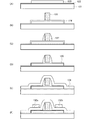
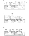
非特許文献1の薄膜トランジスタの構造を、図2に示す。図2では、膜厚200nmの酸化膜が形成された石英の基板あるいはシリコン基板1001上に、膜厚100nmの結晶性半導体膜1002、ゲート酸化膜1003、ゲート電極1005が設けられている。結晶性半導体膜1002上には、膜厚100nmのn型非晶質珪素膜1004a及び1004bが形成されている。
The structure of the thin film transistor of Non-Patent Document 1 is shown in FIG. In FIG. 2, a
さらに、100nmの膜厚の酸化珪素膜1006が形成され、酸化珪素膜1006上には、n型非晶質珪素膜1004a及び1004bそれぞれに接続される、ソース電極及びドレイン電極1007a及び1007bが形成されている。
結晶性半導体膜1002の厚さが厚い(非特許文献1では100nm)と、結晶性半導体膜1002とn型非晶質珪素膜(n+−Si)1004a及び1004bのエッチングレート比が大きくなくても、エッチングを途中で止めることで、結晶性半導体膜1002をエッチングすることなく、n型非晶質珪素膜(n+−Si)1004a及び1004bのみをエッチングできる。
When the
しかしながら、結晶性半導体膜1002の厚さが薄く(例えば40nm以下)なってしまうと、エッチングレートの差があったとしても、n型非晶質珪素膜(n+−Si)1004a及び1004bだけでなく、結晶性半導体膜1002もエッチングしてしまう恐れがある。
However, if the thickness of the
またCMOSトランジスタを形成する場合は、p型非晶質珪素膜(p+−Si)を成膜及びエッチングする必要が生じ、作製工程が複雑かつ不安定になってしまう恐れがある。 In the case of forming a CMOS transistor, it is necessary to form and etch a p-type amorphous silicon film (p + -Si), which may make the manufacturing process complicated and unstable.
第1の半導体膜上に、極薄い、半導体膜の、酸化膜、窒素を含む酸化膜、酸素を含む窒化膜、あるいは窒化膜を形成し、さらに第2の半導体膜を形成する。第2の半導体膜をエッチングする際には、極薄い酸化膜、窒素を含む酸化膜、酸素を含む窒化膜、あるいは窒化膜がエッチングストッパーとなり、第1の半導体膜がエッチングされるのを防ぐ。 On the first semiconductor film, an extremely thin semiconductor film of an oxide film, an oxide film containing nitrogen, a nitride film containing oxygen, or a nitride film is formed, and a second semiconductor film is further formed. When the second semiconductor film is etched, an extremely thin oxide film, an oxide film containing nitrogen, a nitride film containing oxygen, or a nitride film serves as an etching stopper to prevent the first semiconductor film from being etched.
さらに第1と第2の半導体の間の、極薄い、半導体膜の、酸化膜、窒素を含む酸化膜、酸素を含む窒化膜、あるいは窒化膜は、一導電性を付与する不純物元素を導入し、活性化させる加熱処理により、酸素あるいは窒素が拡散し、極薄い、酸化膜、窒素を含む酸化膜、酸素を含む窒化膜、あるいは窒化膜は消滅する。これにより、ソース領域及びドレイン領域が形成される。 Further, an extremely thin semiconductor film, an oxide film, an oxide film containing nitrogen, a nitride film containing oxygen, or a nitride film between the first and second semiconductors is doped with an impurity element imparting one conductivity. By the heat treatment to be activated, oxygen or nitrogen diffuses, and the extremely thin oxide film, oxide film containing nitrogen, nitride film containing oxygen, or nitride film disappears. Thereby, a source region and a drain region are formed.
さらに、一導電性を付与する不純物元素の導入の際に、酸素や窒素が不純物元素による衝突によってはじき出される。そのため酸化膜あるいは窒化膜中の、酸素濃度あるいは窒素濃度が低下する。 Further, when an impurity element imparting one conductivity is introduced, oxygen and nitrogen are ejected by collision with the impurity element. Therefore, the oxygen concentration or nitrogen concentration in the oxide film or nitride film is lowered.
本発明は、以下の半導体装置の作製方法に関するものである。 The present invention relates to the following method for manufacturing a semiconductor device.
本発明は、絶縁表面を有する基板上に、島状半導体膜を形成し、前記島状半導体膜の表面を酸化あるいは窒化して、前記島状半導体膜の表面に、酸化膜、窒素を含む酸化膜、酸素を含む窒化膜、窒化膜、サブオキサイドを含む膜、あるいはサブナイトライドを含む膜のいずれかである第1の絶縁膜を形成し、前記第1の絶縁膜の一部の領域上に、半導体膜を形成し、前記島状半導体膜の表面を酸化あるいは窒化して、前記島状半導体膜表面に、酸化膜、窒素を含む酸化膜、酸素を含む窒化膜、窒化膜のいずれかである第2の絶縁膜を形成し、前記第1の絶縁膜及び、前記第2の絶縁膜をゲート絶縁膜とし、前記ゲート絶縁膜上に、ゲート電極を形成し、前記ゲート電極をマスクとして、前記島状半導体膜及び半導体膜に、一導電型を付与する不純物元素を添加し、前記島状半導体膜及び半導体膜を加熱して、前記島状半導体膜及び半導体膜に添加された前記不純物元素を活性化させ、前記島状半導体膜及び半導体膜を加熱することにより、前記島状半導体膜及び半導体膜の間の前記第1の絶縁膜が消失することを特徴とする半導体装置の作製方法に関する。 In the present invention, an island-shaped semiconductor film is formed over a substrate having an insulating surface, the surface of the island-shaped semiconductor film is oxidized or nitrided, and the surface of the island-shaped semiconductor film is oxidized with an oxide film and nitrogen. Forming a first insulating film that is any one of a film, a nitride film containing oxygen, a nitride film, a film containing suboxide, or a film containing subnitride, over a partial region of the first insulating film; Then, a semiconductor film is formed, and the surface of the island-shaped semiconductor film is oxidized or nitrided, and an oxide film, an oxide film containing nitrogen, a nitride film containing oxygen, or a nitride film is formed on the surface of the island-shaped semiconductor film. A second insulating film is formed, the first insulating film and the second insulating film are used as a gate insulating film, a gate electrode is formed on the gate insulating film, and the gate electrode is used as a mask. And imparting one conductivity type to the island-like semiconductor film and the semiconductor film A pure element is added, the island-like semiconductor film and the semiconductor film are heated, the impurity element added to the island-like semiconductor film and the semiconductor film is activated, and the island-like semiconductor film and the semiconductor film are heated. Accordingly, the present invention relates to a method for manufacturing a semiconductor device, in which the island-shaped semiconductor film and the first insulating film between the semiconductor films disappear.
また本発明は、絶縁表面を有する基板上に、島状半導体膜を形成し、前記島状半導体膜の表面を酸化あるいは窒化して、前記島状半導体膜の表面に、前記島状半導体膜の、酸化膜、窒素を含む酸化膜、酸素を含む窒化膜、窒化膜、サブオキサイドを含む膜、あるいはサブナイトライドを含む膜のいずれかである第1の絶縁膜を形成し、前記第1の絶縁膜の一部の領域上に、半導体膜を形成し、前記島状半導体膜の表面を酸化あるいは窒化して、前記島状半導体膜表面に、酸化膜、窒素を含む酸化膜、酸素を含む窒化膜、窒化膜のいずれかである第2の絶縁膜を形成し、前記第1の絶縁膜並びに前記第2の絶縁膜に、第3の絶縁膜を形成し、前記第3の絶縁膜上に、ゲート電極を形成し、前記ゲート電極をマスクとして、前記島状半導体膜及び半導体膜に、一導電型を付与する不純物元素を添加し、前記島状半導体膜及び半導体膜を加熱して、前記島状半導体膜及び半導体膜に添加された前記不純物元素を活性化させ、前記島状半導体膜及び半導体膜を加熱することにより、前記島状半導体膜及び半導体膜の間の前記第1の絶縁膜が消失することを特徴とする半導体装置の作製方法に関する。 According to the present invention, an island-shaped semiconductor film is formed on a substrate having an insulating surface, the surface of the island-shaped semiconductor film is oxidized or nitrided, and the surface of the island-shaped semiconductor film is formed on the surface of the island-shaped semiconductor film. , An oxide film, an oxide film containing nitrogen, a nitride film containing oxygen, a nitride film, a film containing suboxide, or a film containing subnitride, and forming the first insulating film, A semiconductor film is formed over a partial region of the insulating film, the surface of the island-shaped semiconductor film is oxidized or nitrided, and the surface of the island-shaped semiconductor film includes an oxide film, an oxide film containing nitrogen, and oxygen A second insulating film that is either a nitride film or a nitride film is formed, a third insulating film is formed on the first insulating film and the second insulating film, and the third insulating film is formed on the third insulating film. A gate electrode, and using the gate electrode as a mask, the island-like semiconductor film and An impurity element imparting one conductivity type is added to the conductor film, the island-shaped semiconductor film and the semiconductor film are heated, and the impurity element added to the island-shaped semiconductor film and the semiconductor film is activated, The present invention relates to a method for manufacturing a semiconductor device, wherein the island-shaped semiconductor film and the first insulating film between the island-shaped semiconductor film and the semiconductor film disappear by heating the island-shaped semiconductor film and the semiconductor film.
また本発明は、絶縁表面を有する基板上に、島状半導体膜を形成し、前記島状半導体膜の表面を酸化あるいは窒化して、前記島状半導体膜の表面に、酸化膜、窒素を含む酸化膜、酸素を含む窒化膜、窒化膜、サブオキサイドを含む膜、あるいはサブナイトライドを含む膜のいずれかである第1の絶縁膜を形成し、前記第1の絶縁膜の一部の領域上に、半導体膜を形成し、前記第1の絶縁膜の、前記島状半導体膜と前記半導体膜に挟まれている領域以外を除去して、前記島状半導体膜の中の前記半導体膜が形成されていない領域を露出させ、前記島状半導体膜の表面及び前記半導体膜を酸化あるいは窒化して、酸化膜、窒素を含む酸化膜、酸素を含む窒化膜、窒化膜、サブオキサイドを含む膜、あるいはサブナイトライドを含む膜のいずれかである第2の絶縁膜を形成し、前記島状半導体膜の露出した領域に形成された前記第2の絶縁膜上に、ゲート電極を形成し、前記ゲート電極をマスクとして、前記島状半導体膜及び半導体膜に、一導電型を付与する不純物元素を添加し、前記島状半導体膜及び半導体膜を加熱して、前記島状半導体膜及び半導体膜に添加された前記不純物元素を活性化させ、前記島状半導体膜及び半導体膜を加熱することにより、前記第1の絶縁膜が消失することを特徴とする半導体装置の作製方法に関する。 According to the present invention, an island-shaped semiconductor film is formed over a substrate having an insulating surface, the surface of the island-shaped semiconductor film is oxidized or nitrided, and the surface of the island-shaped semiconductor film includes an oxide film and nitrogen. Forming a first insulating film that is one of an oxide film, a nitride film containing oxygen, a nitride film, a film containing suboxide, or a film containing subnitride, and forming a partial region of the first insulating film; A semiconductor film is formed on the first insulating film except for a region sandwiched between the island-shaped semiconductor film and the semiconductor film, and the semiconductor film in the island-shaped semiconductor film is removed. A region not formed is exposed, and the surface of the island-shaped semiconductor film and the semiconductor film are oxidized or nitrided to form an oxide film, an oxide film containing nitrogen, a nitride film containing oxygen, a nitride film, and a film containing a suboxide. Or any film containing subnitride A second insulating film is formed, a gate electrode is formed on the second insulating film formed in the exposed region of the island-shaped semiconductor film, and the island-shaped semiconductor film is formed using the gate electrode as a mask. And an impurity element imparting one conductivity type is added to the semiconductor film, the island-shaped semiconductor film and the semiconductor film are heated, and the impurity element added to the island-shaped semiconductor film and the semiconductor film is activated, The present invention relates to a method for manufacturing a semiconductor device, wherein the first insulating film disappears by heating the island-shaped semiconductor film and the semiconductor film.
また本発明は、絶縁表面を有する基板上に、島状半導体膜を形成し、前記島状半導体膜の表面を酸化あるいは窒化して、前記島状半導体膜の表面に、酸化膜、窒素を含む酸化膜、酸素を含む窒化膜、窒化膜、サブオキサイドを含む膜、あるいはサブナイトライドを含む膜のいずれかである第1の絶縁膜を形成し、前記第1の絶縁膜の一部の領域上に、半導体膜を形成し、前記第1の絶縁膜の、前記島状半導体膜と前記半導体膜に挟まれている領域以外を除去して、前記島状半導体膜の前記半導体膜が形成されていない領域を露出させ、前記島状半導体膜の露出した領域に、第2の絶縁膜を形成し、前記第2の絶縁膜上に、ゲート電極を形成し、前記ゲート電極をマスクとして、前記島状半導体膜及び半導体膜に、一導電型を付与する不純物元素を添加し、前記島状半導体膜及び半導体膜を加熱して、前記島状半導体膜及び半導体膜に添加された前記不純物元素を活性化させ、前記島状半導体膜及び半導体膜を加熱することにより、前記第1の絶縁膜が消失することを特徴とする半導体装置の作製方法に関する。 According to the present invention, an island-shaped semiconductor film is formed over a substrate having an insulating surface, the surface of the island-shaped semiconductor film is oxidized or nitrided, and the surface of the island-shaped semiconductor film includes an oxide film and nitrogen. Forming a first insulating film that is one of an oxide film, a nitride film containing oxygen, a nitride film, a film containing suboxide, or a film containing subnitride, and forming a partial region of the first insulating film; A semiconductor film is formed thereon, and the first insulating film is removed except for the region sandwiched between the island-shaped semiconductor film and the semiconductor film, so that the semiconductor film of the island-shaped semiconductor film is formed. A second insulating film is formed on the exposed region of the island-shaped semiconductor film, a gate electrode is formed on the second insulating film, and the gate electrode is used as a mask. Impurity sources that impart one conductivity type to island-shaped semiconductor films and semiconductor films And heating the island-shaped semiconductor film and the semiconductor film to activate the impurity element added to the island-shaped semiconductor film and the semiconductor film, and heating the island-shaped semiconductor film and the semiconductor film. The present invention relates to a method for manufacturing a semiconductor device, wherein the first insulating film disappears.
また本発明は、絶縁表面を有する基板上に、島状半導体膜を形成し、前記島状半導体膜上に、絶縁膜を形成し、前記絶縁膜上に、ゲート電極を形成し、前記ゲート電極の側面に、サイドウォールを形成し、前記絶縁膜の、前記ゲート電極及びサイドウォールが形成されていない領域をエッチングし、前記島状半導体膜の前記ゲート電極及びサイドウォールが形成されていない領域を露出させ、前記露出した島状半導体膜を酸化あるいは窒化して、酸化膜、窒素を含む酸化膜、酸素を含む窒化膜、窒化膜、サブオキサイドを含む膜、あるいはサブナイトライドを含む膜のいずれかである第1の絶縁膜を形成し、前記第1の絶縁膜、前記ゲート電極、前記サイドウォールを覆って、第1の半導体膜を形成し、前記第1の半導体膜をエッチングして、前記島状半導体膜及び前記第1の絶縁膜の一部の領域上に、第2の半導体膜を形成し、前記第2の半導体膜及び島状半導体膜に、一導電性を付与する不純物元素を添加し、前記島状半導体膜及び第2の半導体膜を加熱して、前記島状半導体膜及び第2の半導体膜に添加された前記不純物元素を活性化させ、前記島状半導体膜及び第2の半導体膜を加熱することにより、前記島状半導体膜及び第2の半導体膜の間の前記第1の絶縁膜が消失することを特徴とする半導体装置の作製方法に関する。 According to the present invention, an island-shaped semiconductor film is formed on a substrate having an insulating surface, an insulating film is formed on the island-shaped semiconductor film, a gate electrode is formed on the insulating film, and the gate electrode Forming a sidewall on the side surface of the insulating film, etching a region of the insulating film where the gate electrode and the sidewall are not formed, and forming a region of the island-shaped semiconductor film where the gate electrode and the sidewall are not formed. The exposed island-shaped semiconductor film is exposed and oxidized or nitrided to be any of an oxide film, an oxide film containing nitrogen, a nitride film containing oxygen, a nitride film, a film containing suboxide, or a film containing subnitride Forming a first insulating film, covering the first insulating film, the gate electrode, and the sidewall, forming a first semiconductor film, and etching the first semiconductor film; An impurity element which forms a second semiconductor film over a part of the island-shaped semiconductor film and the first insulating film and imparts one conductivity to the second semiconductor film and the island-shaped semiconductor film And the island-like semiconductor film and the second semiconductor film are heated to activate the impurity element added to the island-like semiconductor film and the second semiconductor film, and the island-like semiconductor film and the second semiconductor film are activated. The present invention relates to a method for manufacturing a semiconductor device, in which the first insulating film between the island-shaped semiconductor film and the second semiconductor film disappears by heating the semiconductor film.
本発明において、前記島状半導体膜は珪素を主成分とする結晶性半導体膜であり、前記半導体膜は、珪素を主成分とする半導体膜である。 In the present invention, the island-shaped semiconductor film is a crystalline semiconductor film containing silicon as a main component, and the semiconductor film is a semiconductor film containing silicon as a main component.
本発明において、前記島状半導体膜は珪素を主成分とする結晶性半導体膜であり、前記第1の半導体膜は、珪素を主成分とする半導体膜である。 In the present invention, the island-shaped semiconductor film is a crystalline semiconductor film containing silicon as a main component, and the first semiconductor film is a semiconductor film containing silicon as a main component.
本発明において、前記島状半導体膜は珪素を主成分とする単結晶半導体層であり、前記半導体膜は、珪素を主成分とする半導体膜である。 In the present invention, the island-shaped semiconductor film is a single crystal semiconductor layer containing silicon as a main component, and the semiconductor film is a semiconductor film containing silicon as a main component.
本発明において、前記島状半導体膜は珪素を主成分とする単結晶半導体層であり、前記第1の半導体膜は、珪素を主成分とする半導体膜である。 In the present invention, the island-shaped semiconductor film is a single crystal semiconductor layer containing silicon as a main component, and the first semiconductor film is a semiconductor film containing silicon as a main component.
本発明において、前記3の絶縁膜は、酸化珪素膜、窒素を含む酸化珪素膜、窒化珪素膜、酸素を含む窒化珪素膜のいずれか1つ、あるいは2つ以上の積層膜である。 In the present invention, the third insulating film is a silicon oxide film, a silicon oxide film containing nitrogen, a silicon nitride film, or a silicon nitride film containing oxygen, or a laminated film of two or more.
本発明において、前記2の絶縁膜は、酸化珪素膜、窒素を含む酸化珪素膜、窒化珪素膜、酸素を含む窒化珪素膜のいずれか1つ、あるいは2つ以上の積層膜である。 In the present invention, the second insulating film is a silicon oxide film, a silicon oxide film containing nitrogen, a silicon nitride film, or a silicon nitride film containing oxygen, or a laminated film of two or more.
本発明において、前記酸化膜、窒素を含む酸化膜、酸素を含む窒化膜、窒化膜、サブオキサイドを含む膜、あるいはサブナイトライドを含む膜の膜厚は、0.2nm以上4nm以下である。 In the present invention, the oxide film, the oxide film containing nitrogen, the nitride film containing oxygen, the nitride film, the film containing suboxide, or the film containing subnitride has a thickness of 0.2 nm to 4 nm.
本発明において、前記酸化膜、窒素を含む酸化膜、酸素を含む窒化膜、窒化膜、サブオキサイドを含む膜、あるいはサブナイトライドを含む膜の膜厚は、0.5nm以上3nm以下である。 In the present invention, the oxide film, the oxide film containing nitrogen, the nitride film containing oxygen, the nitride film, the film containing suboxide, or the film containing subnitride has a thickness of 0.5 nm to 3 nm.
なお本明細書において、半導体装置とは、半導体を利用することで機能する素子及び装置全般を指し、半導体を利用することで機能する素子を搭載した電子機器もその範疇とする。 Note that in this specification, a semiconductor device refers to all elements and devices that function by using a semiconductor, and includes electronic devices in which elements that function by using a semiconductor are mounted.
基板を高温で加熱することなく、せり上げ構造のソース領域及びドレイン領域(raised source and drain)を有する薄膜トランジスタを形成することができる。薄膜トランジスタにおいて、半導体膜上にせり上げ構造の低抵抗領域を形成することが可能となる。 A thin film transistor having a raised source and drain region can be formed without heating the substrate at a high temperature. In the thin film transistor, a low resistance region having a raised structure can be formed over the semiconductor film.
せり上げ構造の薄膜トランジスタの作製方法において、活性層である島状半導体膜をエッチングすることなく、せり上げ領域を形成することができる。 In a method for manufacturing a thin film transistor having a raised structure, a raised region can be formed without etching an island-shaped semiconductor film which is an active layer.
以下に本発明を図面を用いて説明する。ただし本発明は多くの異なる態様で実施することが可能であり、本発明の趣旨及びその範囲から逸脱することなくその形態及び詳細を様々に変更し得ることは当業者であれば容易に理解される。従って、本実施の形態の記載内容に限定して解釈されるものではない。 The present invention will be described below with reference to the drawings. However, it will be readily understood by those skilled in the art that the present invention can be implemented in many different modes, and that various modifications can be made without departing from the spirit and scope of the present invention. The Therefore, the present invention is not construed as being limited to the description of this embodiment mode.
なお、実施の形態を説明するための全図において、同一部分又は同様な機能を有する部分には同一の符号を付し、その繰り返しの説明は省略する。 Note that in all the drawings for describing the embodiments, the same portions or portions having similar functions are denoted by the same reference numerals, and repetitive description thereof is omitted.
[実施の形態1] [Embodiment 1]
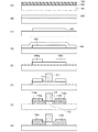
本実施の形態では、せり上げ構造の低抵抗領域を有する薄膜トランジスタの作製方法について、図1(A)〜図1(H)、図10(A)〜図10(E)、図11(A)〜図11(F)、図23(A)〜図23(E)を用いて説明する。 In this embodiment, a method for manufacturing a thin film transistor having a low-resistance region with a raised structure will be described with reference to FIGS. 1A to 1H, FIGS. 10A to 10E, and FIG. This will be described with reference to FIGS. 11 (F) and 23 (A) to 23 (E).
基板101上に、下地絶縁膜102、さらに非晶質半導体膜103を形成する(図1(A)参照)。基板101は、ガラス基板、石英基板等を用いればよく、本実施の形態では、基板101としてガラス基板を用いる。
A
下地絶縁膜102は、酸化珪素膜、窒素を含む酸化珪素膜、酸素を含む窒化珪素膜、窒化珪素膜のいずれか1つの単層膜、あるいはこれらを積層した積層膜を用いればよい。本実施の形態では、下地絶縁膜102として、窒素を含む酸化珪素膜と酸素を含む窒化珪素膜を積層した積層膜を用いる。また必要がなければ下地絶縁膜102を形成しなくてもよい。
As the
基板101としてガラス基板、石英基板等を用いれば、基板101の表面は絶縁性を有している。また下地絶縁膜102を設けた基板101は、やはり絶縁表面を有する基板とみなせる。
If a glass substrate, a quartz substrate, or the like is used as the
本実施の形態では、非晶質半導体膜103として、珪素を主成分とする半導体膜、例えば非晶質珪素膜(アモルファスシリコン膜)を、10〜100nmの膜厚で成膜する。なお半導体膜としてゲルマニウムを主成分とする半導体膜を用いてもよい。珪素あるいはゲルマニウムを主成分とする半導体膜として、珪素膜、ゲルマニウム膜、シリコンゲルマニウム膜が含まれる。
In this embodiment mode, as the
次いで非晶質半導体膜103を、レーザ照射による結晶化、加熱による結晶化等公知の方法で結晶化し、結晶性半導体膜104を形成する(図1(B)参照)。本実施の形態では、非晶質半導体膜103として非晶質珪素膜を成膜したので、結晶性半導体膜104として結晶性珪素膜が形成される。
Next, the
なお、基板101上に下地絶縁膜102及び結晶性半導体膜104を形成する代わりに、SOI(Silicon On Insulator)基板を用いてもよい。
Note that an SOI (Silicon On Insulator) substrate may be used instead of forming the
SOI基板を用いる場合について以下に説明する。 The case where an SOI substrate is used will be described below.
まずSOI構造を有する基板の構造について、図12(A)〜図12(B)、図13(A)〜図13(C)を用いて説明する。 First, a structure of a substrate having an SOI structure will be described with reference to FIGS. 12A to 12B and FIGS. 13A to 13C.
図12(A)において支持基板600は絶縁性を有するものまたは絶縁表面を有するものであり、アルミノシリケートガラス、アルミノホウケイ酸ガラス、バリウムホウケイ酸ガラスのような電子工業用に使われるガラス基板(「無アルカリガラス基板」とも呼ばれる)が適用される。
In FIG. 12A, a supporting
すなわち、支持基板600として、熱膨張係数が25×10−7/℃から50×10−7/℃(好ましくは、30×10−7/℃から40×10−7/℃)であって歪み点が580℃から680℃(好ましくは、600℃から680℃)のガラス基板を適用することができる。その他に石英基板、セラミック基板、表面が絶縁膜で被覆された金属基板などのも適用可能である。
That is, the
LTSS(Low Temperature Single crystal Semiconductor)層601は単結晶半導体層であり、珪素を主成分とする単結晶半導体層、あるいはゲルマニウムを主成分とする単結晶半導体層等、代表的には単結晶シリコン(単結晶珪素)が適用される。
An LTSS (Low Temperature Single Crystal Semiconductor)
その他に、LTSS層601として、水素イオン注入剥離法のようにして単結晶半導体基板もしくは多結晶半導体基板から剥離可能であるガリウムヒ素、インジウムリンなどの化合物半導体による結晶性半導体層を適用することもできる。
In addition, as the
支持基板600とLTSS層601の間には、平滑面を有し親水性表面を形成する接合層602を設ける。この接合層602は平滑面を有し親水性表面を有する層とする。このような表面を形成可能なものとして、化学的な反応により形成される絶縁層が好ましい。例えば、熱的または化学的な反応により形成される酸化半導体膜が適している。主として化学的な反応により形成される膜であれば表面の平滑性を確保できるからである。
A
また、平滑面を有し親水性表面を形成する接合層602は0.2nm乃至500nmの厚さで設けられる。この厚さであれば、被成膜表面の表面荒れを平滑化すると共に、当該膜の成長表面の平滑性を確保することが可能である。
The
LTSS層601がシリコンによるものであれば、酸化性雰囲気下において熱処理により形成される酸化シリコン、酸素ラジカルの反応により成長する酸化シリコン、酸化性の薬液により形成されるケミカルオキサイドなどを接合層602とすることができる。
If the
接合層602としてケミカルオキサイドを用いる場合には0.2nmから3nmの厚さであれば良い。また、好適には化学気相成長法により堆積される酸化シリコンを接合層602とすることができる。この場合、有機シランガスを用いて化学気相成長法により作製される酸化シリコン膜が好ましい。
When chemical oxide is used for the
有機シランガスとしては、珪酸エチル(TEOS:化学式Si(OC2H5)4)、テトラメチルシラン(TMS:化学式Si(CH3)4)、テトラメチルシクロテトラシロキサン(TMCTS)、オクタメチルシクロテトラシロキサン(OMCTS)、ヘキサメチルジシラザン(HMDS)、トリエトキシシラン(SiH(OC2H5)3)、トリスジメチルアミノシラン(SiH(N(CH3)2)3)等のシリコン含有化合物を用いることができる。 Examples of the organic silane gas include ethyl silicate (TEOS: chemical formula Si (OC 2 H 5 ) 4 ), tetramethylsilane (TMS: chemical formula Si (CH 3 ) 4 ), tetramethylcyclotetrasiloxane (TMCTS), and octamethylcyclotetrasiloxane. It is possible to use a silicon-containing compound such as (OMCTS), hexamethyldisilazane (HMDS), triethoxysilane (SiH (OC 2 H 5 ) 3 ), trisdimethylaminosilane (SiH (N (CH 3 ) 2 ) 3 ). it can.
接合層602はLTSS層601側に設けられ、支持基板600の表面と密接することで、室温であっても接合をすることが可能である。より強固に接合を形成するには、支持基板600とLTSS層601を押圧すれば良い。異種材料である支持基板600と接合層602を接合するには表面を清浄化する。支持基板600と接合層602の互いに清浄化された表面を密接させると表面間引力により接合が形成される。
The
さらに、支持基板600の表面に複数の親水基を付着させる処理を加えると、接合を形成するのにより好ましい態様となる。例えば、支持基板600の表面を酸素プラズマ処理もしくはオゾン処理、あるいはオゾン水への浸積処理により親水性にすることが好ましい。
Further, when a treatment for attaching a plurality of hydrophilic groups to the surface of the
このように支持基板600の表面を親水性にする処理を加えた場合には、表面の水酸基が作用して水素結合により接合が形成される。さらに清浄化された表面同士を密接させて接合を形成したものに対して、室温以上の温度で加熱すると接合強度高めることができる。
Thus, when the process which makes the surface of the
異種材料である支持基板600と接合層602を接合するための処理として、接合を形成する表面にアルゴンなどの不活性ガスによるイオンビームを照射して清浄化しても良い。イオンビームの照射により、支持基板600もしくは接合層602の表面に未結合手が露呈して非常に活性な表面が形成される。
As a process for bonding the
このように活性化された表面同士を密接させると、支持基板600と接合層602の接合を低温でも形成することが可能である。表面を活性化して接合を形成する方法は、当該表面を高度に清浄化しておくことが要求されるので、真空中で行うことが好ましい。
When the activated surfaces are brought into close contact with each other, the
LTSS層601は結晶半導体基板を薄片化して形成されるものである。例えば、単結晶半導体基板として単結晶シリコン基板を用いた場合、単結晶シリコン基板の所定の深さに水素クラスターイオン(H2 +、H3 +)を質量分離せずにドープするイオンドープ法でドープし、その後熱処理を行って表層の単結晶シリコン層を剥離して形成することができる。また、水素イオン(H+)や水素クラスターイオンをイオン注入法を用いて注入してもよい。
The
また、ポーラスシリコン(多孔性シリコン)上に単結晶シリコンをエピタキシャル成長させた後、ポーラスシリコン層をウォータージェットで劈開して剥離する方法を適用しても良い。LTSS層601の厚さは5nm乃至500nm、好ましくは10nm乃至200nmの厚さである。
Alternatively, a method may be applied in which single crystal silicon is epitaxially grown on porous silicon (porous silicon), and then the porous silicon layer is cleaved and peeled off with a water jet. The thickness of the
図12(B)は支持基板600にバリア層603と接合層602を設けた構成を示す。バリア層603を設けることで、支持基板600として用いられるガラス基板からアルカリ金属もしくはアルカリ土類金属のような可動イオン不純物が拡散してLTSS層601が汚染されることを防ぐことができる。バリア層603上には接合層602を設けることが好ましい。
FIG. 12B illustrates a structure in which a
支持基板600において、不純物の拡散を防止するバリア層603と接合強度を確保する接合層602とによる機能が異なる複数の層を設けることにより、支持基板の選択範囲を広げることができる。LTSS層601側にも接合層602を設けておくことが好ましい。すなわち、支持基板600にLTSS層601を接合するに際し、接合を形成する面の一方もしくは双方に接合層602を設けることが好ましく、それにより接合強度を高めることができる。
By providing the
図13(A)はLTSS層601と接合層602の間に絶縁層604を設けた構成を示す。絶縁層604は窒素を含有する絶縁層であることが好ましい。例えば、窒化シリコン膜、酸素を含む窒化シリコン膜もしくは窒素を含む酸化シリコン膜から選ばれた1つまたは複数の膜を積層して形成することができる。
FIG. 13A illustrates a structure in which an insulating
例えば、絶縁層604として、LTSS層601側から窒素を含む酸化シリコン膜、酸素を含む窒化シリコン膜を積層した積層膜を用いることができる。接合層602が支持基板600と接合を形成する機能を有するのに対し、絶縁層604は不純物によりLTSS層601が汚染されることを防止する。
For example, as the insulating
なお、ここで窒素を含む酸化シリコン膜とは、その組成として、窒素よりも酸素の含有量が多いものであって、濃度範囲として酸素が55原子%〜65原子%、窒素が0.5原子%〜20原子%、Siが25原子%〜35原子%、水素が0.1原子%〜15原子%の範囲で含まれるものをいう。また、酸素を含む窒化シリコン膜とは、その組成として、酸素よりも窒素の含有量が多いものであって、濃度範囲として酸素が5原子%〜30原子%、窒素が20原子%〜50原子%原子%、Siが25原子%〜35原子%、水素が15原子%〜25原子%の範囲で含まれるものをいう。 Note that the silicon oxide film containing nitrogen has a composition that contains more oxygen than nitrogen, and the concentration ranges from 55 atomic% to 65 atomic% and nitrogen is 0.5 atomic%. % To 20 atom%, Si is contained in the range of 25 atom% to 35 atom%, and hydrogen is contained in the range of 0.1 atom% to 15 atom%. The silicon nitride film containing oxygen has a composition containing more nitrogen than oxygen, and the concentration ranges of oxygen are 5 atomic% to 30 atomic% and nitrogen is 20 atomic% to 50 atoms. % Atomic%, Si is included in a range of 25 atomic% to 35 atomic%, and hydrogen is included in a range of 15 atomic% to 25 atomic%.
図13(B)は、支持基板600に接合層602を設けた構成である。支持基板600と接合層602との間にはバリア層603が設けられていることが好ましい。支持基板600として用いられるガラス基板からアルカリ金属もしくはアルカリ土類金属のような可動イオン不純物が拡散してLTSS層601が汚染されることを防ぐためである。LTSS層601には直接酸化で形成された酸化シリコン層605が形成されている。この酸化シリコン層605が接合層602と接合を形成し、支持基板600上にLTSS層601を固定する。酸化シリコン層605は熱酸化により形成されたものが好ましい。
FIG. 13B illustrates a structure in which a
図13(C)は、支持基板600に接合層602を設けた別の構成である。支持基板600と接合層602との間にはバリア層603が設けられている。
FIG. 13C illustrates another structure in which the
図13(C)では、バリア層603は一層または複数の層をもって構成する。例えば、ナトリウムなどのイオンをブロッキングする効果の高い窒化シリコン膜または酸素を含む窒化シリコン膜を第1層目として用い、その上層に第2層目として酸化シリコン膜または窒素を含む酸化シリコン膜を設ける。
In FIG. 13C, the
バリア層603の第1層目は不純物の拡散を防止する目的を持った絶縁膜であり緻密な膜であるのに対し、第2層目は第1層目の膜の内部応力が上層に作用しないように、応力を緩和することを一つの目的としている。このように支持基板600にバリア層603を設けることで、LTSS層を接合する際の基板の選択範囲を広げることができる。
The first layer of the
バリア層603には接合層602が形成されており、支持基板600とLTSS層601を固定する。
A
図12(A)〜図12(B)、図13(A)〜図13(C)に示すSOI構造を有する基板の作製方法について、図14(A)〜図14(C)、図15(A)〜図15(B)、図16(A)〜図16(C)、図17(A)〜図17(C)、図18(A)〜図18(B)、図19(A)〜図19(C)を用いて説明する。 FIGS. 14A to 14C and FIG. 15B illustrate a method for manufacturing a substrate having an SOI structure illustrated in FIGS. 12A to 12B and FIGS. 13A to 13C. A) to FIG. 15B, FIG. 16A to FIG. 16C, FIG. 17A to FIG. 17C, FIG. 18A to FIG. 18B, and FIG. This will be described with reference to FIG.
清浄化された半導体基板606の表面から電界で加速されたイオンを所定の深さに注入して分離層607を形成する(図14(A)参照)。半導体基板606に形成される分離層607の深さは、イオンの加速電圧とイオンの入射角によって制御する。半導体基板606の表面からイオンの平均進入深さに近い深さ領域に分離層607が形成される。例えば、LTSS層の厚さは5nm乃至500nm、好ましくは10nm乃至200nmの厚さであり、イオンを注入する際の加速電圧はこのような厚さを考慮して行われる。イオンの注入はイオンドーピング装置を用いて行うことが好ましい。すなわち、ソースガスをプラズマ化して生成された複数のイオン種を質量分離しないで注入するドーピング方式を用いる。
Ions accelerated by an electric field are implanted to a predetermined depth from the cleaned surface of the
本実施の形態の場合、一または複数の同一の原子から成る質量の異なるイオンを注入することが好ましい。イオンドーピングは、加速電圧10kVから100kV、好ましくは30kVから80kV、ドーズ量は1×10¹⁶/cm2から4×1016/cm2、ビーム電流密度が2μA/cm2以上、好ましくは5μA/cm2以上、より好ましくは10μA/cm2以上とすれば良い。 In the case of this embodiment, it is preferable to implant ions having different masses composed of one or more identical atoms. Ion doping has an acceleration voltage of 10 kV to 100 kV, preferably 30 kV to 80 kV, a dose of 1 × 10 16 / cm 2 to 4 × 10 16 / cm 2 , and a beam current density of 2 μA / cm 2 or more, preferably 5 μA / cm. It may be 2 or more, more preferably 10 μA / cm 2 or more.
水素イオンをドープあるいは注入する場合には、H+、H2 +、H3 +イオンを含ませると共に、H3 +イオンの割合を高めておくことが好ましい。水素イオンをドープあるいは注入する場合には、H+、H2 +、H3 +イオンを含ませると共に、H3 +イオンの割合を高めておくと注入効率を高めることができ、ドープ時間を短縮することができる。それにより、半導体基板606に形成される分離層607の領域には1×10²⁰/cm3(好ましくは5×1020/cm3)以上の水素を含ませることが可能である。
When doping or implanting hydrogen ions, it is preferable to include H + , H 2 + , H 3 + ions and to increase the ratio of H 3 + ions. When doping or implanting hydrogen ions, H + , H 2 + , H 3 + ions are included, and if the ratio of H 3 + ions is increased, the implantation efficiency can be increased and the doping time is shortened. can do. Accordingly, hydrogen of 1 × 10 20 / cm 3 (preferably 5 × 10 20 / cm 3 ) or more can be contained in the region of the
半導体基板606中において、局所的に高濃度の水素ドープ領域を形成すると、結晶構造が乱されて微小な空孔が形成される。分離層607を形成することができる。この場合、比較的低温の熱処理によって分離層607に含まれる水素ガスの圧力が上昇し、分離層607に沿って劈開することにより薄いLTSS層を形成することができる。
When a high-concentration hydrogen-doped region is locally formed in the
イオンを質量分離して半導体基板606に注入しても、上記と同様に分離層607を形成することができる。この場合にも、質量の大きいイオン(例えばH3 +イオン)を選択的に注入することは上記と同様な効果を奏することとなり好ましい。
Even when ions are mass-separated and implanted into the
イオンを生成するイオン種を生成するガスとしては水素の他に重水素、ヘリウムのような不活性ガスを選択することも可能である。原料ガスにヘリウムを用い、質量分離機能を有さないイオンドーピング装置を用いることにより、He+イオンの割合が高いイオンビームが得ることができる。このようなイオンを半導体基板606に注入することで、微小な空孔を形成することができ上記と同様な分離層607を半導体基板606中に設けることができる。
In addition to hydrogen, an inert gas such as deuterium or helium can be selected as a gas that generates ionic species that generate ions. By using helium as the source gas and an ion doping apparatus that does not have a mass separation function, an ion beam having a high ratio of He + ions can be obtained. By implanting such ions into the
分離層607の形成に当たってはイオンを高ドーズ条件で注入する必要があり、半導体基板606の表面が粗くなってしまう場合がある。そのためイオンが注入される表面に緻密な膜を設けておいても良い。例えば、窒化シリコン膜もしく酸素を含むは窒化シリコン膜などによりイオン注入に対する保護膜を50nm乃至200nmの厚さで設けておいても良い。
In forming the
次に、支持基板600と接合を形成する面に接合層602として酸化シリコン膜を形成する(図14(B)参照)。酸化シリコン膜の厚さは10nm乃至200nm、好ましくは10nm乃至100nm、より好ましくは20nm乃至50nmとすれば良い。
Next, a silicon oxide film is formed as a
酸化シリコン膜としては上述のように有機シランガスを用いて化学気相成長法により作製される酸化シリコン膜が好ましい。その他に、シランガスを用いて化学気相成長法により作製される酸化シリコン膜を適用することもできる。化学気相成長法による成膜では、単結晶半導体基板に形成した分離層607から脱ガスが起こらない温度として、例えば350℃以下の成膜温度が適用される。また、単結晶もしくは多結晶半導体基板からLTSS層を剥離する熱処理は、成膜温度よりも高い熱処理温度が適用される。
As the silicon oxide film, a silicon oxide film formed by a chemical vapor deposition method using an organosilane gas as described above is preferable. In addition, a silicon oxide film manufactured by a chemical vapor deposition method using silane gas can be used. In film formation by chemical vapor deposition, for example, a film formation temperature of 350 ° C. or lower is applied as a temperature at which degassing does not occur from the
支持基板600と、半導体基板606の接合層602が形成された面を対向させ、密接させることで接合を形成する(図14(C)参照)。接合を形成する面は十分に清浄化しておく。そして、支持基板600と接合層602を密接させることにより接合が形成される。接合は初期の段階においてファンデルワールス力が作用するものと考えられ、支持基板600と半導体基板606とを圧接することで水素結合により強固な接合を形成することが可能である。
The
良好な接合を形成するために、表面を活性化しておいても良い。例えば、接合を形成する面に原子ビームもしくはイオンビームを照射する。原子ビームもしくはイオンビームを利用する場合には、アルゴン等の不活性ガス中性原子ビームもしくは不活性ガスイオンビームを用いることができる。その他に、プラズマ照射もしくはラジカル処理を行う。このような表面処理により200℃乃至400℃の温度であっても異種材料間の接合強度を高めることが可能となる。 In order to form a good bond, the surface may be activated. For example, the surface on which the junction is formed is irradiated with an atomic beam or an ion beam. When an atomic beam or an ion beam is used, an inert gas neutral atom beam or inert gas ion beam such as argon can be used. In addition, plasma irradiation or radical treatment is performed. Such surface treatment makes it possible to increase the bonding strength between different kinds of materials even at a temperature of 200 ° C. to 400 ° C.
半導体基板606と支持基板600を重ね合わせた状態で第1の熱処理を行う。第1の熱処理により支持基板600上に薄い半導体層(LTSS層)を残して半導体基板606を分離を行う(図15(A)参照)。第1の熱処理は接合層602の成膜温度以上で行うことが好ましく、400℃以上700℃未満の温度で行うことが好ましい。この温度範囲で熱処理を行うことで分離層607に含まれる水素ガスの圧力が上昇し、分離層607に沿って半導体層を劈開することができる。接合層602は支持基板600と接合しているので、支持基板600上には半導体基板606と同じ結晶性のLTSS層601が固定された形態となる。
A first heat treatment is performed in a state where the
また第1の熱処理の前に、400℃未満の熱活性を行い接合を強化してもよい。具体的には、200℃で1分〜120分で加熱処理する。 Further, before the first heat treatment, thermal activation of less than 400 ° C. may be performed to strengthen the bonding. Specifically, heat treatment is performed at 200 ° C. for 1 minute to 120 minutes.
次に支持基板600にLTSS層601が接合された状態で第2の熱処理を行う(図15(B)参照)。第2の熱処理は、第1の熱処理温度よりも高い温度であって支持基板600の歪み点を超えない温度で行うことが好ましい。或いは、第1の熱処理と第2の熱処理は同じ温度であっても、第2の熱処理の処理時間を長くすることが好ましい。熱処理は、熱伝導加熱、対流加熱または輻射加熱などにより支持基板600及び/またはLTSS層601が加熱されるようにすれば良い。熱処理装置としては電熱炉、ランプアニール炉などを適用することができる。第2の熱処理は多段階に温度を変化させて行っても良い。また瞬間熱アニール(RTA)装置を用いても良い。RTA装置によって熱処理を行う場合には、基板の歪み点近傍またはそれよりも若干高い温度に加熱することもできる。
Next, second heat treatment is performed in a state where the
第2の熱処理は、イオンをドープすることによって結晶性が損なわれたLTSS層601の結晶性を回復させるために有効である。さらに、第2の熱処理は、半導体基板606を支持基板600と接合させ他後、第1の熱処理によって分割する際に生じるLTSS層601のダメージを回復させることにも有効である。また、第1の熱処理と第2の熱処理を行うことで水素結合を、より強固な共有結合に変化させることができる。
The second heat treatment is effective for recovering the crystallinity of the
その後、さらにレーザ光を照射するのが望ましい。レーザ光の照射により、LTSS層601の少なくとも一部が溶融し、再結晶化することになり、結晶欠陥が修復される。
Thereafter, it is desirable to further irradiate with laser light. By irradiation with laser light, at least a part of the
LTSS層601の表面をより平坦化する目的で化学的機械研磨(CMP)処理を行っても良い。CMP処理は第1の熱処理後もしくは第2の熱処理後に行うことができる。尤も、第2の熱処理前に行えば、LTSS層601の表面を平坦化すると共にCMP処理によって生じる表面の損傷層を第2の熱処理で修復することができる。
Chemical mechanical polishing (CMP) treatment may be performed for the purpose of further flattening the surface of the
いずれにしても、第1の熱処理と第2の熱処理を本形態のように組み合わせて行うことで、ガラス基板のような熱的に脆弱な支持基板の上に、結晶性に優れた結晶半導体層を設けることが可能となる。 In any case, by performing the first heat treatment and the second heat treatment in combination as in this embodiment, a crystalline semiconductor layer having excellent crystallinity on a thermally fragile support substrate such as a glass substrate Can be provided.
図14(A)〜図14(C)及び図15(A)〜図15(B)の工程を経て、図12(A)に示すSOI基板が形成される。 Through the steps of FIGS. 14A to 14C and FIGS. 15A to 15B, the SOI substrate shown in FIG. 12A is formed.
図12(B)に示すSOI構造の基板を作成する方法について、図18(A)〜図18(B)を用いて説明する。 A method for manufacturing the SOI structure substrate illustrated in FIG. 12B will be described with reference to FIGS.
図14(A)〜図14(B)に示す作製工程に基づいて、半導体基板606中に分離層607を形成し、さらに、半導体基板606の、支持基板600と接合を形成する面に、接合層602を形成する。
14A to 14B, the
次いで、バリア層603及び接合層602が形成された支持基板600と、半導体基板606の接合層602を密着させて接合を形成する(図18(A)参照)。
Next, the
この状態で第1の熱処理を行う。第1の熱処理は接合層602の成膜温度以上で行うことが好ましく、400℃以上700℃未満の温度で行うことが好ましい。それにより分離層607に含まれる水素ガスの圧力が上昇し、半導体基板606を劈開することができる。支持基板600上には半導体基板606と同じ結晶性を有するLTSS層601が形成される(図18(B)参照)。
In this state, a first heat treatment is performed. The first heat treatment is preferably performed at a temperature equal to or higher than the deposition temperature of the
また第1の熱処理の前に、400℃未満の熱活性を行い接合を強化してもよい。具体的には、200℃で1分〜120分で加熱処理する。 Further, before the first heat treatment, thermal activation of less than 400 ° C. may be performed to strengthen the bonding. Specifically, heat treatment is performed at 200 ° C. for 1 minute to 120 minutes.
次に支持基板600にLTSS層601が接合された状態で第2の熱処理を行う。第2の熱処理は、第1の熱処理温度よりも高い温度であって支持基板600の歪み点を超えない温度で行うことが好ましい。或いは、第1の熱処理と第2の熱処理は同じ温度であっても、第2の熱処理の処理時間を長くすることが好ましい。熱処理は、熱伝導加熱、対流加熱または輻射加熱などにより支持基板600及び/またはLTSS層601が加熱されるようにすれば良い。第2の熱処理を行うことでLTSS層601に残留する応力を緩和することができ、第1の熱処理によって分割する際に生じるLTSS層601のダメージを回復させることにも有効である。
Next, second heat treatment is performed in a state where the
その後、さらにレーザ光を照射するのが望ましい。レーザ光の照射により、LTSS層601の少なくとも一部が溶融し、再結晶化することになり、結晶欠陥が修復される。
Thereafter, it is desirable to further irradiate with laser light. By irradiation with laser light, at least a part of the
以上のようにして、図12(B)に示すSOI基板が形成される。 As described above, the SOI substrate shown in FIG. 12B is formed.
次いで図13(A)に示すSOI構造の基板の作製方法について、図19(A)〜図19(C)を用いて説明する。 Next, a method for manufacturing the SOI structure substrate illustrated in FIG. 13A will be described with reference to FIGS.
まず図14(A)に示す作製工程に基づいて、半導体基板606中に分離層607を形成する。
First, the
次に、半導体基板606の表面に絶縁層604を形成する。絶縁層604は窒素を含有する絶縁層であることが好ましい。例えば、窒化シリコン膜、酸素を含む窒化シリコン膜もしくは窒素を含む酸化シリコン膜から選ばれた1つまたは複数の膜を積層して形成することができる。
Next, the insulating
さらに、絶縁層604上に接合層602として酸化シリコン膜を形成する(図19(A)参照)。
Further, a silicon oxide film is formed as the
支持基板600と、半導体基板606の接合層602が形成された面を対向させ、密接させることで接合を形成する(図19(B)参照)。
The
この状態で第1の熱処理を行う。第1の熱処理は接合層602の成膜温度以上で行うことが好ましく、400℃以上700℃未満の温度で行うことが好ましい。それにより分離層607に含まれる水素ガスの圧力が上昇し、半導体基板606を劈開することができる。支持基板600上には半導体基板606と同じ結晶性を有するLTSS層601が形成される(図19(C)参照)。
In this state, a first heat treatment is performed. The first heat treatment is preferably performed at a temperature equal to or higher than the deposition temperature of the
また第1の熱処理の前に、400℃未満の熱活性を行い接合を強化してもよい。具体的には、200℃で1分〜120分で加熱処理する。 Further, before the first heat treatment, thermal activation of less than 400 ° C. may be performed to strengthen the bonding. Specifically, heat treatment is performed at 200 ° C. for 1 minute to 120 minutes.
次に支持基板600にLTSS層601が接合された状態で第2の熱処理を行う。第2の熱処理は、第1の熱処理温度よりも高い温度であって支持基板600の歪み点を超えない温度で行うことが好ましい。或いは、第1の熱処理と第2の熱処理は同じ温度であっても、第2の熱処理の処理時間を長くすることが好ましい。熱処理は、熱伝導加熱、対流加熱または輻射加熱などにより支持基板600及び/またはLTSS層601が加熱されるようにすれば良い。第2の熱処理を行うことでLTSS層601に残留する応力を緩和することができ、第1の熱処理によって分割する際に生じるLTSS層601のダメージを回復させることにも有効である。
Next, second heat treatment is performed in a state where the
その後、さらにレーザ光を照射するのが望ましい。レーザ光の照射により、LTSS層601の少なくとも一部が溶融し、再結晶化することになり、結晶欠陥が修復される。
Thereafter, it is desirable to further irradiate with laser light. By irradiation with laser light, at least a part of the
図19(A)〜図19(C)に示すように、絶縁層604を半導体基板606上に形成すると、絶縁層604によって不純物がLTSS層601に混入するのを防ぐので、LTSS層601が汚染されるのを防止することが可能となる。
As shown in FIGS. 19A to 19C, when the insulating
図16(A)〜図16(C)は、支持基板側に接合層を設けてLTSS層を有するSOI構造の基板を製造する工程を示す。 16A to 16C illustrate a process of manufacturing an SOI structure substrate having an LTSS layer by providing a bonding layer on the support substrate side.
まず、酸化シリコン層605が形成された半導体基板606に電界で加速されたイオンを所定の深さに注入し、分離層607を形成する(図16(A)参照)。酸化シリコン層605は、半導体基板606上に酸化シリコン層をスパッタ法やCVD法で成膜してもよいし、半導体基板606が単結晶シリコン基板の場合、半導体基板606を熱酸化して形成してもよい。本実施の形態では、半導体基板606が単結晶シリコン基板として、酸化シリコン層605は単結晶シリコン基板を熱酸化して形成する。
First, ions accelerated by an electric field are implanted to a predetermined depth into a
半導体基板606へのイオンの注入は図14(A)の場合と同様である。半導体基板606の表面に酸化シリコン層605を形成しておくことでイオン注入によって表面がダメージを受け、平坦性が損なわれるのを防ぐことができる。
Ion implantation into the
バリア層603及び接合層602が形成された支持基板600と半導体基板606の酸化シリコン層605が形成された面を密着させて接合を形成する(図16(B)参照)。
A
この状態で第1の熱処理を行う。第1の熱処理は接合層602の成膜温度以上で行うことが好ましく、400℃以上700℃未満の温度で行うことが好ましい。それにより分離層607に含まれる水素ガスの圧力が上昇し、半導体基板606を劈開することができる。支持基板600上には半導体基板606と同じ結晶性を有するLTSS層601が形成される(図16(C)参照)。
In this state, a first heat treatment is performed. The first heat treatment is preferably performed at a temperature equal to or higher than the deposition temperature of the
また第1の熱処理の前に、400℃未満の熱活性を行い接合を強化してもよい。具体的には、200℃で1分〜120分で加熱処理する。 Further, before the first heat treatment, thermal activation of less than 400 ° C. may be performed to strengthen the bonding. Specifically, heat treatment is performed at 200 ° C. for 1 minute to 120 minutes.
次に支持基板600にLTSS層601が接合された状態で第2の熱処理を行う。第2の熱処理は、第1の熱処理温度よりも高い温度であって支持基板600の歪み点を超えない温度で行うことが好ましい。或いは、第1の熱処理と第2の熱処理は同じ温度であっても、第2の熱処理の処理時間を長くすることが好ましい。熱処理は、熱伝導加熱、対流加熱または輻射加熱などにより支持基板600及び/またはLTSS層601が加熱されるようにすれば良い。第2の熱処理を行うことでLTSS層601に残留する応力を緩和することができ、第1の熱処理によって分割する際に生じるLTSS層601のダメージを回復させることにも有効である。
Next, second heat treatment is performed in a state where the
その後、さらにレーザ光を照射するのが望ましい。レーザ光の照射により、LTSS層601の少なくとも一部が溶融し、再結晶化することになり、結晶欠陥が修復される。
Thereafter, it is desirable to further irradiate with laser light. By irradiation with laser light, at least a part of the
以上のようにして、図13(B)に示すSOI基板が形成される。 As described above, the SOI substrate shown in FIG. 13B is formed.
図17(A)〜図17(C)は支持基板側に接合層を設けてLTSS層を接合する場合における他の例を示す。 17A to 17C show other examples in the case where a bonding layer is provided on the support substrate side and the LTSS layer is bonded.
最初に半導体基板606に分離層607を形成する(図17(A)参照)。分離層607を形成するためのイオンの注入はイオンドーピング装置を用いて行う。この工程では電界で加速された質量の異なるイオンが高電界で加速されて半導体基板606に照射される。
First, the
このとき、半導体基板606の表面はイオンの照射により平坦性が損なわれるおそれがあるので、保護膜として酸化シリコン層605を設けておくことが好ましい。酸化シリコン層605は熱酸化により形成しても良いし、ケミカルオキサイドを適用しても良い。ケミカルオキサイドは酸化性の薬液に半導体基板606を浸すことで形成可能である。例えば、オゾン含有水溶液で半導体基板606を処理すれば表面にケミカルオキサイドが形成される。
At this time, since the flatness of the surface of the
また保護膜として、プラズマCVD法で形成した窒素を含む酸化シリコン膜、酸素を含む窒化シリコン膜、またはTEOSを用いて成膜した酸化シリコン膜を用いてもよい。 Alternatively, a silicon oxide film containing nitrogen, a silicon nitride film containing oxygen, or a silicon oxide film formed using TEOS may be used as the protective film.
支持基板600にはバリア層603を設けることが好ましい。バリア層603を設けることで、支持基板600として用いられるガラス基板からアルカリ金属もしくはアルカリ土類金属のような可動イオン不純物が拡散してLTSS層601が汚染されることを防ぐことができる。
The
バリア層603は一層または複数の層をもって構成する。例えば、ナトリウムなどのイオンをブロッキングする効果の高い窒化シリコン膜または酸素を含む窒化シリコン膜を第1層目として用い、その上層に第2層目として酸化シリコン膜または窒素を含む酸化シリコン膜を設ける。
The
バリア層603の第1層目は不純物の拡散を防止する目的を持った絶縁膜であり緻密な膜であるのに対し、第2層目は第1層目の膜の内部応力が上層に作用しないように、応力を緩和することを一つの目的としている。このように支持基板600にバリア層603を設けることで、LTSS層を接合する際の基板の選択範囲を広げることができる。
The first layer of the
バリア層603の上層に接合層602を設けた支持基板600と半導体基板606を接合させる(図17(B)参照)。半導体基板606の表面は保護膜として設けた酸化シリコン層605をフッ酸で除去しておき、半導体表面が露出する状態となっている。半導体基板606の最表面はフッ酸溶液の処理により水素で終端されている状態であれば良い。接合形成に際して表面終端水素により水素結合が形成され、良好な接合を形成することができる。
The
また、不活性ガスのイオンを照射して半導体基板606の最表面に未結合手が露出するようにして、真空中で接合を形成しても良い。
Alternatively, a bond may be formed in a vacuum by irradiating ions of an inert gas so that dangling bonds are exposed on the outermost surface of the
この状態で第1の熱処理を行う。第1の熱処理は接合層602の成膜温度以上で行うことが好ましく、400℃以上700℃未満の温度で行うことが好ましい。それにより分離層607に含まれる水素ガスの圧力が上昇し、半導体基板606を劈開することができる。支持基板600上には半導体基板606と同じ結晶性を有するLTSS層601が形成される(図17(C)参照)。
In this state, a first heat treatment is performed. The first heat treatment is preferably performed at a temperature equal to or higher than the deposition temperature of the
また第1の熱処理の前に、400℃未満の熱活性を行い接合を強化してもよい。具体的には、200℃で1分〜120分で加熱処理する。 Further, before the first heat treatment, thermal activation of less than 400 ° C. may be performed to strengthen the bonding. Specifically, heat treatment is performed at 200 ° C. for 1 minute to 120 minutes.
次に支持基板600にLTSS層601が接合された状態で第2の熱処理を行う。第2の熱処理は、第1の熱処理温度よりも高い温度であって支持基板600の歪み点を超えない温度で行うことが好ましい。或いは、第1の熱処理と第2の熱処理は同じ温度であっても、第2の熱処理の処理時間を長くすることが好ましい。
Next, second heat treatment is performed in a state where the
熱処理は、熱伝導加熱、対流加熱または輻射加熱などにより支持基板600及び/またはLTSS層601が加熱されるようにすれば良い。第2の熱処理を行うことでLTSS層601に残留する応力を緩和することができ、第1の熱処理によって分割する際に生じるLTSS層601のダメージを回復させることにも有効である。
In the heat treatment, the
その後、さらにレーザ光を照射するのが望ましい。レーザ光の照射により、LTSS層601の少なくとも一部が溶融し、再結晶化することになり、結晶欠陥が修復される。
Thereafter, it is desirable to further irradiate with laser light. By irradiation with laser light, at least a part of the
以上のようにして図13(C)に示すSOI基板を形成する。 In this manner, the SOI substrate shown in FIG. 13C is formed.
次いで結晶性半導体膜104あるいはLTSS層601をマスクを用いてエッチングし、島状半導体膜105を形成する(図1(C)参照)。
Next, the
島状半導体膜105をオゾン水または過酸化水素水で処理する、あるいは島状半導体膜105をUVオゾン法で酸化して、島状半導体膜105の表面に島状半導体膜の酸化膜107を形成する。この酸化膜107の膜厚はごく薄く、0.2nm〜4nm、好ましくは、0.5nm〜3nmである。
The island-shaped
また島状半導体膜105を窒化することにより、酸化膜107の代わりに窒化膜を形成することも可能である。
Further, a nitride film can be formed instead of the
また酸化膜107あるいは窒化膜の形成前に、島状半導体膜105表面の自然酸化膜を希フッ酸で除去してもよい。
Further, the natural oxide film on the surface of the island-shaped
島状半導体膜105の窒化工程として、例えばプラズマ窒化処理が挙げられる。プラズマ窒化処理とは、高真空状態の反応室にアンモニアガス、窒素ガス、または一酸化二窒素ガス(N2O)を導入し、高周波電力を印加することによってプラズマを発生させる処理である。島状半導体膜105にプラズマ窒化処理を行うと、島状半導体膜105の表面に、ごく薄い窒化膜が形成される。さらにプラズマ窒化処理を行う反応室に酸素ガスを混合してもよい。
As a nitriding step of the island-shaped
あるいは、上記の工程により酸化膜107を形成した後に、窒化処理を行うことによって酸化膜の表面を窒化させ、酸化膜107の代わりに酸素を含む窒化膜を形成しても良い。サブオキサイドあるいはサブナイトライドは、10%〜40%、好ましくは30%〜40%含まれる。
Alternatively, after the
本明細書において、サブオキサイドとは、X線光電子分光(X−ray Photoelectron Spectroscopy:XPS)、あるいは、ESCA(Electron Spectroscopy for Chemical Analysis)とも言われる)での測定結果により、便宜上、Si2O、SiO、Si2O3で表されるものをいい、また便宜上、珪素の電荷はそれぞれ、Si1+、Si2+、Si3+となる。なおSiO2成分ではSi4+となる。 In this specification, the suboxide is, for convenience, Si 2 O, based on the measurement result in X-ray photoelectron spectroscopy (XPS) or ESCA (also referred to as Electron Spectroscopy for Chemical Analysis). The term “SiO” or “Si 2 O 3” is used. For convenience, the charges of silicon are Si 1+ , Si 2+ , and Si 3+ , respectively. In addition, it becomes Si 4+ in the SiO 2 component.
サブオキサイドが10%〜40%というのは、便宜上Si2O、SiO、Si2O3で表される珪素の酸化物及びSiO2で表される珪素の酸化物全体のうち、Si2O、SiO、Si2O3で表される珪素の酸化物が、珪素の酸化物全体の10%〜40%であるということである。 The suboxide is 10% to 40% for the sake of convenience, Si 2 O, SiO, silicon oxide represented by Si 2 O 3 and silicon oxide represented by SiO 2 , Si 2 O, This means that the silicon oxide represented by SiO and Si 2 O 3 is 10% to 40% of the entire silicon oxide.
なおサブナイトライドについては、サブオキサイドの酸素が窒素に置き換わっただけで、上記の考え方と同様である。 The subnitride is the same as the above-mentioned concept, except that oxygen in the suboxide is replaced with nitrogen.
酸化膜107の代わりに窒化膜、あるいは酸素を含む窒化膜を形成する場合でも、それぞれの膜厚は、0.2nm〜4nm、好ましくは、0.5nm〜3nmである。
Even when a nitride film or a nitride film containing oxygen is formed instead of the
また、島状半導体膜105を酸化あるいは窒化せずに、半導体膜のごく薄い酸化膜、あるいは、半導体膜のごく薄い窒化膜を、CVD法等で、島状半導体膜105の表面上に形成してもよい。その場合にでも、それぞれの膜厚は、0.2nm〜4nm、好ましくは、0.5nm〜3nmがよい。サブオキサイドあるいはサブナイトライドは、10%〜40%、好ましくは30%〜40%含まれる。
Further, without oxidizing or nitriding the island-shaped
例えば、モノシラン(SiH4)と一酸化二窒素(N2O)の混合ガスを用いて、プラズマCVD法により、島状半導体膜105の表面上に酸素と含む窒化珪素膜または窒素を含む酸化珪素膜をごく薄い厚さで成膜することができる。
For example, a silicon nitride film containing oxygen or silicon oxide containing nitrogen is formed on the surface of the island-shaped
島状半導体膜105をオゾン水または過酸化水素水で処理する、あるいは島状半導体膜105をUVオゾン法で酸化して、島状半導体膜105の表面に形成された酸化膜107、及び、酸化膜107の代わりに形成可能である以下の膜、すなわち、島状半導体膜105にプラズマ窒化処理を行うことにより、島状半導体膜105の表面に形成されるごく薄い窒化膜、酸化膜107を形成しさらに窒化処理を行うことで形成される酸素を含む窒化膜、島状半導体膜105の表面上にCVD法等で形成するごく薄い酸化膜、あるいは、ごく薄い窒化膜を、本明細書では、「第1の絶縁膜」と呼ぶことにする。サブオキサイドあるいはサブナイトライドは、10%〜40%、好ましくは30%〜40%含まれる。
An
また第1の絶縁膜形成前に、希フッ酸で島状半導体膜105表面の自然酸化膜を除去してもよい。
Further, the natural oxide film on the surface of the island-shaped
酸化膜107を形成後、島状半導体膜105及び酸化膜107上に、半導体膜108を膜厚10〜50nmの厚さで成膜する(図1(D)参照)。
After the
半導体膜108は、非晶質半導体膜、結晶性半導体膜、微結晶性半導体膜(「セミアモルファス半導体膜」ともいう)のいずれかであればよい。
The
なおセミアモルファス半導体(本明細書では「Semi−amorphous Smiconductor(SAS)」ともいう)膜とは、非晶質半導体と結晶構造を有する半導体(単結晶、多結晶を含む)膜の中間的な構造の半導体を含む膜である。このセミアモルファス半導体膜は、自由エネルギー的に安定な第3の状態を有する半導体膜であって、短距離秩序を持ち格子歪みを有する結晶質なものであり、その粒径を0.5〜20nmとして非単結晶半導体膜中に分散させて存在せしめることが可能である。なお微結晶半導体膜(マイクロクリスタル半導体膜)もセミアモルファス半導体膜に含まれる。 Note that a semi-amorphous semiconductor (also referred to as “Semi-amorphous Semiconductor (SAS)” in this specification) film is an intermediate structure between an amorphous semiconductor and a semiconductor (including single crystal and polycrystal) films having a crystal structure. It is a film | membrane containing the semiconductor of. This semi-amorphous semiconductor film is a semiconductor film having a third state that is stable in terms of free energy, and is a crystalline film having short-range order and lattice distortion, and has a grain size of 0.5 to 20 nm. And can be dispersed in the non-single-crystal semiconductor film. Note that a microcrystalline semiconductor film is also included in the semi-amorphous semiconductor film.
セミアモルファス半導体膜の1つの例として、セミアモルファス珪素膜が挙げられる。セミアモルファス珪素膜は、そのラマンスペクトルが520cm−1よりも低波数側にシフトしており、またX線回折ではSi結晶格子に由来するとされる(111)、(220)の回折ピークが観測される。また、未結合手(ダングリングボンド)を終端化させるために水素またはハロゲンを少なくとも1原子%またはそれ以上含ませている。本明細書では便宜上、このような珪素膜をセミアモルファス珪素膜と呼ぶ。さらに、ヘリウム、アルゴン、クリプトン、ネオンなどの希ガス元素を含ませて格子歪みをさらに助長させることで安定性が増し良好なセミアモルファス半導体膜が得られる。 One example of the semi-amorphous semiconductor film is a semi-amorphous silicon film. The semi-amorphous silicon film has its Raman spectrum shifted to a lower wavenumber than 520 cm −1, and (111) and (220) diffraction peaks that are attributed to the Si crystal lattice are observed in X-ray diffraction. The Further, in order to terminate dangling bonds (dangling bonds), at least 1 atomic% or more of hydrogen or halogen is contained. In this specification, such a silicon film is referred to as a semi-amorphous silicon film for convenience. Further, by adding a rare gas element such as helium, argon, krypton, or neon to further promote lattice distortion, stability is improved and a good semi-amorphous semiconductor film can be obtained.
またセミアモルファス珪素膜は珪素(シリコン)を含む気体をグロー放電分解することにより得ることができる。代表的な珪素(シリコン)を含む気体としては、SiH4であり、その他にもSi2H6、SiH2Cl2、SiHCl3、SiCl4、SiF4などを用いることができる。また水素や、水素にヘリウム、アルゴン、クリプトン、ネオンから選ばれた一種または複数種の希ガス元素を加えたガスで、この珪素(シリコン)を含む気体を希釈して用いることで、セミアモルファス珪素膜の形成を容易なものとすることができる。希釈率は2倍〜1000倍の範囲で珪素(シリコン)を含む気体を希釈することが好ましい。またさらに、珪素(シリコン)を含む気体中に、CH4、C2H6などの炭化物気体、GeH4、GeF4などのゲルマニウム化気体、F2などを混入させて、エネルギーバンド幅を1.5〜2.4eV、若しくは0.9〜1.1eVに調節しても良い。 The semi-amorphous silicon film can be obtained by glow discharge decomposition of a gas containing silicon (silicon). A typical gas containing silicon (Si) is SiH 4 , and Si 2 H 6 , SiH 2 Cl 2 , SiHCl 3 , SiCl 4 , SiF 4, and the like can be used. Semi-amorphous silicon is also obtained by diluting and using hydrogen or a gas containing silicon (silicon) with one or more kinds of rare gas elements selected from helium, argon, krypton, and neon. The film can be easily formed. It is preferable to dilute the gas containing silicon (silicon) in the range of a dilution rate of 2 to 1000 times. Furthermore, a gas containing silicon (silicon) is mixed with a carbide gas such as CH 4 or C 2 H 6 , a germanium gas such as GeH 4 or GeF 4 , F 2, etc. You may adjust to 5-2.4 eV or 0.9-1.1 eV.
本実施の形態では、半導体膜108として珪素を主成分とする半導体膜、例えば非晶質珪素膜を用いる。またゲルマニウムを主成分とする半導体膜を用いてもよい。珪素あるいはゲルマニウムをす成分とする半導体膜には、珪素膜、ゲルマニウム膜、シリコンゲルマニウム膜が含まれる。
In this embodiment mode, a semiconductor film containing silicon as a main component, for example, an amorphous silicon film is used as the
また本実施の形態では、半導体膜108として、一導電性を付与する不純物元素を添加されていない非晶質珪素膜、いわゆる真性非晶質珪素膜、あるいはi型非晶質珪素膜を用いるが、これに限定されない。半導体膜108として、n型を付与する不純物元素、例えば、リン(P)やヒ素(As)を添加された半導体膜、いわゆるn型半導体膜を用いてもよいし、p型を付与する不純物元素、例えばホウ素(B)を添加された半導体膜、いわゆるp型半導体膜を用いてもよい。
In this embodiment mode, an amorphous silicon film to which an impurity element imparting one conductivity is not added, a so-called intrinsic amorphous silicon film, or an i-type amorphous silicon film is used as the
次いで、半導体膜108をエッチングして、島状半導体膜105の端部に近い領域上に半導体膜109(半導体膜109a及び半導体膜109b)を形成する(図1(E)参照)。半導体膜108をエッチングする際に、酸化膜107がエッチングストッパとなり、島状半導体膜105がエッチングされてしまうのを防ぐ。もし酸化膜107が形成されていないと、半導体膜108をエッチングする際に、島状半導体膜105までエッチングされてしまい、島状半導体膜105がえぐれてしまう恐れがある。なお半導体膜108のエッチングはドライエッチングでもよいし、ウエットエッチングでもよい。
Next, the
本実施の形態では、アルカリ性溶液を用いウエットエッチングにて、半導体膜108をエッチングする。アルカリ性溶液として、テトラメチルアンモニウムハイドロオキサイド(TMAH)や水酸化カリウムを用い、50℃〜70℃に熱してウェットエッチングに用いる。
In this embodiment, the
次いで島状半導体膜105を酸化して、新たに酸化膜を得る。本明細書では「第2の絶縁膜」と呼ぶ。第2の絶縁膜と酸化膜107(第1の絶縁膜)とを合わせて、ゲート絶縁膜115とする。なお島状半導体膜105を酸化する前に、酸化膜107(第1の絶縁膜)を除去しておいてもよい。その場合は、島状半導体膜105を新たに酸化して得られた酸化膜(第2の絶縁膜)をゲート絶縁膜とする(後述及び図23(A)〜図23(E)参照)。なお、実際には半導体膜109上にも酸化膜ができると可能性があるが、図1(F)〜図1(H)では省略している。
Next, the island-shaped
次いで、島状半導体膜105及び酸化膜107上で、半導体膜109が形成されていない領域に、ゲート電極111を形成する(図1(F)参照)。
Next, a
ゲート電極111は、クロム(Cr)、タンタル(Ta)、タングステン(W)、チタン(Ti)、アルミニウム(Al)、窒化タンタル等のいずれか1つ、あるいは2つ以上を積層した積層膜を用いて形成することができる。
As the
次いでゲート電極111をマスクとして、半導体膜109に一導電性を付与する不純物元素を添加する。n型を付与する不純物元素としては、例えばリン(P)やヒ素(As)を用いてもよい。またp型を付与する不純物元素としては、例えばホウ素(B)を用いてもよい。
Next, an impurity element imparting one conductivity is added to the semiconductor film 109 using the
一導電性を付与する不純物元素は、イオンドーピング法やイオン注入法で添加され、加速電圧(印加電圧ともいう)は、5〜80kVで行う。この添加工程の際に、半導体膜のごく薄い酸化膜107、本実施の形態ではごく薄い酸化珪素膜中の構成元素である酸素や珪素等にイオンが衝突して、酸素や珪素が散乱あるいは跳躍するイオンミキシングが生じる。一導電性を付与する不純物元素は、1×10¹⁴〜1×10¹⁶atoms/cm2の範囲で添加すればよく、異なる加速電圧で2回以上添加してもよい。
An impurity element imparting one conductivity is added by an ion doping method or an ion implantation method, and an acceleration voltage (also referred to as an applied voltage) is 5 to 80 kV. During this addition process, ions collide with the very
不純物元素添加工程により、島状半導体膜105中のゲート電極111の下の領域に、チャネル形成領域118が形成される。島状半導体膜105中の不純物元素が添加された領域及び半導体膜109は、不純物領域114(不純物領域114a及び不純物領域114b)となる。不純物領域114中のごく薄い酸化膜107はイオンミキシングされた酸化膜116(酸化膜116a及び酸化膜116b)となる(図1(G)参照)。
Through the impurity element addition step, a
その後、レーザ活性化や、RTA(Rapid Thermal Anneal)や、炉を用いたファーネスアニール等を用いて、添加された不純物元素の活性化を行う。特に、レーザ活性化やRTAによって、島状半導体膜105と半導体膜109が700℃以上、特に1000℃以上になると、酸素の拡散が進み、イオンミキシングされた酸化膜116の少なくとも一部は消失する。またレーザ活性化時に酸化膜116及びその周辺の半導体膜が溶融すれば、酸化膜116は消失しやすくなる。同時に、島状半導体膜105の結晶状態を反映した、半導体膜109の結晶成長、エピタキシャル成長が進行する。これにより半導体膜109がn型あるいはp型に低抵抗化され、n型あるいはp型の結晶性半導体膜となる。またレーザ活性化やRTAは、短時間の処理なのでガラス基板が溶融せず、また大きく変形させないという利点がある。
Thereafter, activation of the added impurity element is performed using laser activation, RTA (Rapid Thermal Anneal), furnace annealing using a furnace, or the like. In particular, when the island-shaped
以上により、チャネル形成領域118と、ソース領域またはドレイン領域の一方である領域119aと、ソース領域またはドレイン領域の他方である領域119bが形成される(図1(H)参照)。
Through the above steps, the
なお上述のように、島状半導体膜105を酸化する前に、酸化膜107(第1の絶縁膜)を除去し、島状半導体膜105を新たに酸化して得られた酸化膜(第2の絶縁膜)をゲート絶縁膜とする場合を、図23(A)〜図23(E)を用いて説明する。なお図1(A)〜図1(H)と同じものは同じ符号で表されている。
As described above, before the island-shaped
まず図1(A)〜図1(E)の作製工程を経て、図23(A)に示す構造を得る。なお図23(A)は、図1(E)と同じ構造を示している。 First, the structure shown in FIG. 23A is obtained through the manufacturing steps shown in FIGS. Note that FIG. 23A illustrates the same structure as FIG.
次いで、酸化膜107の島状半導体膜105と半導体膜109に挟まれている領域以外の領域、すなわち酸化膜107中の露出している領域を除去し、島状半導体膜105の半導体膜109(109a及び109b)が形成されていない領域を露出させる(図23(B)参照)。
Next, a region other than the region between the island-shaped
次いで、島状半導体膜105を酸化あるいは窒化して、新たに酸化膜、窒素を含む酸化膜、酸素を含む窒化膜、あるいは、窒化膜を得る。本実施の形態では酸化膜165を得る。なお実際には半導体膜109上にも酸化膜ができると可能性があるが、図23(C)〜図23(E)では省略している。酸化膜165は、ゲート絶縁膜として機能する。ゲート絶縁膜たる酸化膜165上に、ゲート電極111を形成する(図23(C)参照)。
Next, the island-shaped
あとは図1(G)〜図1(H)の作製工程に基づいて、不純物添加工程、加熱工程等を行う(図23(D)〜図23(E)参照)。 After that, an impurity addition step, a heating step, and the like are performed based on the manufacturing steps of FIGS. 1G to 1H (see FIGS. 23D to 23E).
また図1(H)のゲート絶縁膜115上に第2のゲート絶縁膜166を形成してもよい。図10(A)〜図10(D)に第2のゲート絶縁膜166した場合の作製工程を示す。
Alternatively, the second
まず図1(E)の半導体膜109(109a及び109b)を形成するまでの工程を行った後、島状半導体膜105を酸化して、新たに酸化膜(本明細書では「第2の絶縁膜」ともいう)を形成する。第1の絶縁膜である酸化膜107と第2の絶縁膜を合わせて、酸化膜117とする(図10(A)参照)。なお、実際には半導体膜109上にも酸化膜ができると可能性があるが、図10(A)〜図10(E)では省略する。
First, after the steps up to the formation of the semiconductor film 109 (109a and 109b) in FIG. 1E are performed, the island-shaped
次いで、絶縁膜110(本明細書では「第3の絶縁膜ともいう)を、島状半導体膜105、半導体膜109a及び109b、酸化膜117を覆って形成する(図10(B)参照)。
Next, an insulating film 110 (also referred to as a “third insulating film” in this specification) is formed to cover the island-shaped
次いで絶縁膜110上にゲート電極111を形成して、ゲート電極111をマスクとして、絶縁膜110をエッチングして、第1のゲート絶縁膜115上の第2のゲート絶縁膜166とする(図10(C)参照)。
Next, a
第2のゲート絶縁膜166は、酸化珪素膜、窒素を含む酸化珪素膜、窒化珪素膜、酸素を含む窒化珪素膜のいずれか1つ、あるいは2つ以上の積層膜を用いて形成すればよい。
The second
その後図1(G)〜図1(H)の作製工程に基づいて、薄膜トランジスタを作製する(図10(D)〜図10(E)参照)。 After that, a thin film transistor is manufactured based on the manufacturing steps of FIGS. 1G to 1H (see FIGS. 10D to 10E).
また半導体膜109(109a及び109b)を形成後、酸化膜107の島状半導体膜105と半導体膜109に挟まれている領域以外の領域、すなわち酸化膜107中の露出している領域を除去し、島状半導体膜105の半導体膜109(109a及び109b)が形成されていない領域を露出させる。そして島状半導体膜105の露出した領域上に、新たにゲート絶縁膜151を形成してもよい。酸化膜107の露出している領域を除去し、島状半導体膜105の半導体膜109(109a及び109b)が形成されていない領域を露出させ、ゲート絶縁膜151を形成する工程について、図11(A)〜図11(F)を用いて説明する。
After forming the semiconductor film 109 (109a and 109b), a region other than the region sandwiched between the island-shaped
ただし上述の通り、酸化膜107の代わりに窒化膜や酸素を含む窒化膜を用いてもよい。
However, as described above, a nitride film or a nitride film containing oxygen may be used instead of the
まず図1(A)〜図1(E)に示す作製工程に基づいて、半導体膜109(109a及び109b)を形成するまでの工程を行う(図11(A)参照)。次いで半導体膜109(109a及び109b)をマスクとして、露出している酸化膜107(あるいは窒化膜や酸素を含む窒化膜)を除去する。これにより酸化膜107は、島状半導体膜105と半導体膜109に挟まれた領域のみが残存する(図11(B)参照)。
First, steps up to formation of the semiconductor film 109 (109a and 109b) are performed based on the manufacturing steps illustrated in FIGS. 1A to 1E (see FIG. 11A). Next, the exposed oxide film 107 (or a nitride film or a nitride film containing oxygen) is removed using the semiconductor film 109 (109a and 109b) as a mask. Thus, only the region between the island-shaped
次いで島状半導体膜105の、酸化膜107が除去された領域上に、ゲート絶縁膜151を形成する(図11(C)参照)。ゲート絶縁膜151は、酸化珪素膜、窒素を含む酸化珪素膜、窒化珪素膜、酸素を含む窒化珪素膜のいずれか1つ、あるいは2つ以上の積層膜を用いて形成すればよい。
Next, a
次いでゲート絶縁膜151上にゲート電極111を形成する(図11(D)参照)。その後図1(G)〜図1(H)の作製工程に基づいて、薄膜トランジスタを作製する(図11(E)〜図11(F)参照)。
Next, the
[実施の形態2]
本実施の形態では、実施の形態1とは異なる構造を有する薄膜トランジスタの作製方法について、図3(A)〜図3(F)、図4(A)〜図4(C)、図8(A)〜図8(E)、図9(A)〜図9(C)を用いて説明する。
[Embodiment 2]
In this embodiment, a method for manufacturing a thin film transistor having a structure different from that in Embodiment 1 will be described with reference to FIGS. 3A to 3F, 4A to 4C, and 8A. ) To FIG. 8E and FIG. 9A to FIG. 9C.
実施の形態1に基づいて、図1(C)に示す作製工程までを行う。図3(A)は図1(C)と同じであり、基板121、下地絶縁膜122、島状半導体膜123は、それぞれ基板101、下地絶縁膜102、島状半導体膜105に対応している。
Based on Embodiment Mode 1, the manufacturing steps shown in FIG. 3A is the same as FIG. 1C, and the
次いで、島状半導体膜123を覆って絶縁膜124を形成し、島状半導体膜123及び絶縁膜124上に、ゲート電極125を形成する。ゲート電極125はゲート電極111と同様にして形成すればよい(図3(B)参照)。
Next, an insulating
なおゲート電極125を形成後、一導電型を付与する不純物元素を島状半導体膜123に導入してもよい。このときの不純物元素の濃度は、後述する不純物領域141(不純物領域141a及び不純物領域141b)を形成するための不純物元素添加工程の際の、不純物濃度より低いものとする。
Note that after the
次いで島状半導体膜123、絶縁膜124、ゲート電極125上に絶縁膜を形成し、異方性エッチングを行って、ゲート電極125の側面にサイドウォール127を形成する(図3(C)参照)。
Next, an insulating film is formed over the island-shaped
次いで、絶縁膜124の、ゲート電極125及びサイドウォール127が形成されていない領域をエッチングにより除去し、露出した島状半導体膜123をオゾン水または過酸化水素水で処理する、あるいは露出した島状半導体膜123をUVオゾン法で酸化して、島状半導体膜123の表面に島状半導体膜の酸化膜129を形成する(図3(D)参照)。この酸化膜129の膜厚はごく薄く、0.5〜3nmである。
Next, a region of the insulating
酸化膜129、サイドウォール127、ゲート電極125を覆って、半導体膜131を成膜する(図3(E)参照)。半導体膜131は、非晶質半導体膜、結晶性半導体膜、微結晶性半導体膜(「セミアモルファス半導体膜」ともいう)のいずれかであればよい。
A
半導体膜131を成膜したら、半導体膜131上で、島状半導体膜123の端部に近い領域上に、レジストマスク132(132a及び132b)を形成する(図3(F)参照)。
After the
次いでレジストマスク132をマスクとして、半導体膜131をエッチングする。半導体膜131をエッチングする際に、酸化膜129がエッチングストッパとなり、島状半導体膜123がエッチングされてしまうのを防ぐ。
Next, the
本実施の形態では、ウエットエッチングにより半導体膜131をエッチングする。
In this embodiment mode, the
これにより島状半導体膜123の端部に近い領域上に半導体膜135(135a及び135b)を形成する(図4(A)参照)。 Thus, a semiconductor film 135 (135a and 135b) is formed over a region near the end of the island-shaped semiconductor film 123 (see FIG. 4A).
また半導体膜131を成膜しエッチングして半導体膜135を形成する代わりに、ポリシランとシクロペンタシランを含む有機溶媒を塗布して、インクジェット法で、酸化膜129上に選択的に珪素膜を形成してもよい。
Instead of forming the
あるいは半導体膜131を成膜する代わりにポリシランとシクロペンタシランを含む有機溶媒を塗布後に焼成してから、レジストマスク132を形成し、エッチングにより半導体膜135を形成してもよい。
Alternatively, instead of forming the
次いでゲート電極125、サイドウォール127をマスクとして、半導体膜135に一導電性を付与する不純物元素を添加する。n型を付与する不純物元素としては、例えばリン(P)やヒ素(As)を用いてもよい。またp型を付与する不純物元素としては、例えばホウ素(B)を用いてもよい。
Next, an impurity element imparting one conductivity is added to the semiconductor film 135 using the
一導電性を付与する不純物元素は、イオンドーピング法やイオン注入法で添加され、加速電圧(印加電圧ともいう)は、5〜80kVで行う。この添加工程の際に、ごく薄い酸化膜129、本実施の形態ではごく薄い酸化珪素膜中の構成元素である酸素や珪素等にイオンが衝突して、酸素や珪素が散乱あるいは跳躍するイオンミキシングが生じる。一導電性を付与する不純物元素は、1×10¹⁴〜1×10¹⁶atoms/cm2の範囲で添加すればよく、異なる加速電圧で2回以上添加してもよい。
An impurity element imparting one conductivity is added by an ion doping method or an ion implantation method, and an acceleration voltage (also referred to as an applied voltage) is 5 to 80 kV. During this addition process, ions collide with a very
不純物元素添加工程により、島状半導体膜123中のゲート電極125、サイドウォール127の下の領域に、チャネル形成領域146が形成される。またチャネル形成領域146上にはゲート絶縁膜142が形成される。島状半導体膜123中の不純物元素が添加された領域と半導体膜135は、不純物領域141(不純物領域141a及び不純物領域141b)となる。不純物領域141中のごく薄い酸化膜129はイオンミキシングされた酸化膜143(半導体膜の酸化膜143a及び半導体膜の酸化膜143b)となる(図4(B)参照)。
Through the impurity element addition step, a
その後、レーザ活性化や、RTA(Rapid Thermal Anneal)や、炉を用いたファーネスアニール等を用いて、添加された不純物の活性化を行う。特に、レーザ活性化やRTAによって、島状半導体膜123と半導体膜135が700℃以上、特に1000℃以上になると、酸素の拡散が進み、イオンミキシングされた酸化膜143の少なくとも一部は消失する。またレーザ活性化時に酸化膜143及びその周辺の半導体膜が溶融すれば、酸化膜143は消失しやすくなる。同時に、島状半導体膜123の結晶状態を反映した、半導体膜135の結晶成長、エピタキシャル成長が進行する。これにより半導体膜135がn型あるいはp型に低抵抗化され、半導体膜135がn型あるいはp型の結晶性半導体膜となる。
Thereafter, the added impurities are activated by laser activation, RTA (Rapid Thermal Anneal), furnace annealing using a furnace, or the like. In particular, when the island-shaped
以上により、チャネル形成領域146と、ソース領域またはドレイン領域の一方である領域147aと、ソース領域またはドレイン領域の他方である領域147bが形成される(図4(C)参照)。
Through the above steps, the
また図3(B)に示すゲート電極125を形成後、ゲート電極125上に絶縁膜126を形成しても良い(図8(A)参照)。絶縁膜126は、酸化珪素膜、窒素を含む酸化珪素膜、窒化珪素膜、酸素を含む窒化珪素膜のいずれか1つ、あるいは2つ以上の積層膜を用いて形成すればよい。
Alternatively, after the
その後、図3(C)〜図3(F)及び図4(A)〜図4(C)に示す工程と同じ工程を経て薄膜トランジスタが作製される(図8(B)〜図8(E)及び図9(A)〜図9(C)参照)。 Thereafter, a thin film transistor is manufactured through the same steps as those shown in FIGS. 3C to 3F and FIGS. 4A to 4C (FIGS. 8B to 8E). And FIG. 9 (A) to FIG. 9 (C)).
[実施の形態3]
本実施の形態では、無線交信可能な半導体装置において、実施の形態1〜実施の形態2のTFTを用いた場合について、図5、図6(A)〜図6(B)を用いて説明する。
[Embodiment 3]
In this embodiment, the case where the TFTs of Embodiments 1 to 2 are used in a semiconductor device capable of wireless communication is described with reference to FIGS. 5 and 6A to 6B. .
図5に示すように、本実施の形態の無線交信可能な半導体装置200は、演算処理回路201、記憶回路202、アンテナ203、電源回路204、復調回路205、変調回路206を有する。無線交信可能な半導体装置200は、アンテナ203と電源回路204を必須の構成要素としており、他の要素は、無線交信可能な半導体装置200の用途に従って、適宜設けられる。
As illustrated in FIG. 5, the semiconductor device 200 capable of wireless communication according to this embodiment includes an arithmetic processing circuit 201, a
実施の形態1〜実施の形態2に基づいて作製されたTFTは、演算処理回路201、記憶回路202、電源回路204、復調回路205、変調回路206に適用可能である。
TFTs manufactured based on Embodiment Modes 1 to 2 can be applied to the arithmetic processing circuit 201, the
演算処理回路201は、復調回路205から入力される信号に基づき、命令の解析、記憶回路202の制御、外部に送信するデータの変調回路206への出力などを行う。
Based on the signal input from the demodulation circuit 205, the arithmetic processing circuit 201 performs analysis of instructions, control of the
記憶回路202は、記憶素子を含む回路と、データの書き込みやデータの読み出しを行う制御回路を有する。記憶回路202には、少なくとも、半導体装置自体の個体識別番号が記憶されている。個体識別番号は、他の半導体装置と区別するために用いられる。また、記憶回路202は、実施の形態1または実施の形態2で述べたTFTを用いて形成すればよい。
The
アンテナ203は、リーダ/ライタ207から供給された搬送波を、交流の電気信号に変換する。また、変調回路206により、負荷変調が加えられる。電源回路204は、アンテナ203が変換した交流の電気信号を用いて電源電圧を生成し、各回路に電源電圧を供給する。 The antenna 203 converts the carrier wave supplied from the reader / writer 207 into an AC electrical signal. Further, load modulation is applied by the modulation circuit 206. The power supply circuit 204 generates a power supply voltage using the AC electrical signal converted by the antenna 203 and supplies the power supply voltage to each circuit.
復調回路205は、アンテナ203が変換した交流の電気信号を復調し、復調した信号を、演算処理回路201に供給する。変調回路206は、演算処理回路201から供給される信号に基づき、アンテナ203に負荷変調を加える。 The demodulation circuit 205 demodulates the AC electrical signal converted by the antenna 203 and supplies the demodulated signal to the arithmetic processing circuit 201. The modulation circuit 206 applies load modulation to the antenna 203 based on the signal supplied from the arithmetic processing circuit 201.
リーダ/ライタ207は、アンテナ203に加えられた負荷変調を、搬送波として受信する。また、リーダ/ライタ207は、搬送波を無線交信可能な半導体装置200に送信する。なお、搬送波とは、リーダ/ライタ207が送受信する電磁波であり、リーダ/ライタ207は変調回路206により変調された搬送波を受信する。 The reader / writer 207 receives the load modulation applied to the antenna 203 as a carrier wave. The reader / writer 207 transmits the carrier wave to the semiconductor device 200 capable of wireless communication. Note that the carrier wave is an electromagnetic wave transmitted and received by the reader / writer 207, and the reader / writer 207 receives the carrier wave modulated by the modulation circuit 206.
図6(A)に示すのは記憶素子をマトリクス状に配置した記憶回路202の構成の一例である。記憶回路202上にメモリセル521がマトリクス状に設けられたメモリセルアレイ523、カラムデコーダ525と読み出し回路526とセレクタ527を有するビット線駆動回路524、ロウデコーダ530とレベルシフタ531を有するワード線駆動回路529、書き込み回路等を有し外部とのやりとりを行うインターフェース528を有している。なお、ここで示す記憶回路202の構成はあくまで一例であり、センスアンプ、出力回路、バッファ等の他の回路を有していてもよいし、書き込み回路をビット線駆動回路に設けてもよい。
FIG. 6A illustrates an example of a structure of the
メモリセル521は、ワード線Wy(0≦y≦n)を構成する第1の配線と、ビット線Bx(0≦x≦m)を構成する第2の配線と、TFT532と、記憶素子533とを有する。
The
次に、本発明のメモリセルへの書き込み及び読み込み動作について、図6(B)を参照しながら説明する。なお、ここではメモリセルに「0」が書き込まれた状態を第2の状態、「1」が書き込まれた状態を第1の状態とする。 Next, writing and reading operations to the memory cell of the present invention will be described with reference to FIG. Here, the state in which “0” is written in the memory cell is the second state, and the state in which “1” is written is the first state.
まず、メモリセル521に「0」を書き込むための回路動作の一例を述べる。書き込み処理は、メモリセル521のワード線W0を選択し、ビット線B0に電流を流すことで行われる。つまり、書き込みを行いたいメモリセルをワード線W0により選択し、記憶素子533が第1の状態から第2の状態へ移行し、絶縁させることが可能な電圧をかければよい。例えば、この電圧を10Vとする。このとき、他のメモリセル内の記憶素子506、記憶素子507及び記憶素子508に書き込みが行われることを防止するためにTFT502、TFT503及びTFT504をオフにする。例えばワード線W1及びビット線B1は0Vとしておくとよい。ワード線W0のみが選択された状態で、ビット線B0に、記憶素子533を第1の状態から第2の状態へと移行するのに十分な電圧をかけることで、記憶素子533に「0」が書き込まれた状態にすることができる。
First, an example of a circuit operation for writing “0” to the
次に、メモリセル521の読み出し操作の例を示す。読み出し操作は、メモリセル521の記憶素子533に「1」が書き込まれた第1の状態であるか、「0」が書き込まれた第2の状態であるかを判別すればよい。例えば、メモリセル521に「0」が書き込まれている状態であるか、「1」が書き込まれている状態であるかを読み出す場合について説明する。記憶素子533は「0」が書き込まれた状態、つまり、絶縁状態である。ワード線W0を選択してTFT532をオンにする。ここで、TFT532がオンの状態でビット線B0に所定の電圧以上の電圧をかける。ここでは、所定の電圧を5Vとする。このとき、記憶素子533が第1の状態、つまり、絶縁されていない状態であれば、電流はメモリセル521内の接地している配線へと流れてしまい、ビット線B0の電圧は0Vになる。逆に、記憶素子533が第2の状態、つまり、絶縁状態であれば、電流はメモリセル521内の接地している配線に流れてしまうことなく、ビット線B0の電圧は5Vで維持される。このように、ビット線の電圧により「0」が書き込まれているか、「1」が書き込まれているかを判別することができる。
Next, an example of a read operation of the
例えば、図6(B)に示される、TFT532、TFT503、TFT502、TFT504を、それぞれ、実施の形態1の図1(H)に示すTFT、実施の形態2の図4(C)に示すTFTのいずれかを用いることが可能である。
For example, the
以上のようにして、本発明のTFTは無線交信可能な半導体装置に適用することが可能である。 As described above, the TFT of the present invention can be applied to a semiconductor device capable of wireless communication.
[実施の形態4]
実施の形態3に基づいて作製された、無線交信可能な半導体装置200は、電磁波の送信と受信ができるという機能を活用して、様々な物品やシステムに用いることができる。物品とは、例えば、鍵(図7(A)参照)、紙幣、硬貨、有価証券類、無記名債券類、証書類(運転免許証や住民票等、図7(B)参照)、書籍類、容器類(シャーレ等、図7(C)参照)、包装用容器類(包装紙やボトル等、図7(E)及び図7(F)参照)、記録媒体(ディスクやビデオテープ等)、乗物類(自転車等)、装身具(鞄や眼鏡等、図7(D)参照)、食品類、衣類、生活用品類、電子機器(液晶表示装置、EL表示装置、テレビジョン装置、携帯端末等)等である。
[Embodiment 4]
The semiconductor device 200 capable of wireless communication manufactured based on Embodiment 3 can be used for various articles and systems by utilizing a function of transmitting and receiving electromagnetic waves. Goods include, for example, keys (see FIG. 7A), banknotes, coins, securities, bearer bonds, certificates (driver's license, resident's card, etc., see FIG. 7B), books, Containers (such as petri dishes, see FIG. 7C), packaging containers (such as wrapping paper and bottles, see FIGS. 7E and 7F), recording media (discs, video tapes, etc.), vehicles Types (bicycles, etc.), accessories (such as bags and glasses, see FIG. 7D), foods, clothing, daily necessities, electronic devices (liquid crystal display devices, EL display devices, television devices, portable terminals, etc.), etc. It is.
本発明を適用して作製された、無線交信可能な半導体装置200は、上記のような様々な形状の物品の表面に貼り付けたり、埋め込んだりして、固定される。また、システムとは、物品管理システム、認証機能システム、流通システム等であり、本発明の半導体装置を用いることにより、システムの高機能化、多機能化、高付加価値化を図ることができる。 The semiconductor device 200 capable of wireless communication manufactured by applying the present invention is fixed by being attached or embedded on the surface of an article having various shapes as described above. The system is an article management system, an authentication function system, a distribution system, or the like. By using the semiconductor device of the present invention, the system can be enhanced in function, multifunctional, and added value.
[実施の形態5]
本実施の形態では、単結晶半導体基板を用いてトランジスタを作製する例を、図20(A)〜図20(E)、図21(A)〜図21(D)、図22(A)〜図22(C)を用いて説明する。
[Embodiment 5]
In this embodiment, an example in which a transistor is manufactured using a single crystal semiconductor substrate is described with reference to FIGS. 20A to 20E, FIGS. 21A to 21D, and FIGS. This will be described with reference to FIG.
まずp型半導体基板701にn型半導体領域702を形成する(図20(A)参照)。なお、p型半導体基板701の代わりにn型半導体基板、及び、n型半導体領域702の代わりにp型半導体領域を用いてもよい。
First, an n-
n型半導体領域702の境界に溝703を形成する(図20(B)参照)。次いでp型半導体基板701を加熱して、溝703から熱酸化させ、酸化物705を形成する。酸化物705により、後の工程で完成されるnチャネル型トランジスタとpチャネル型トランジスタが絶縁分離される。
A
次いで実施の形態1に基づいて、p型半導体基板701及びn型半導体領域702上に、ごく薄い半導体の酸化膜、ごく薄い窒素を含む半導体の酸化膜、ごく薄い酸素を含む半導体の窒化膜、あるいは、ごく薄い半導体の窒化膜を形成する。図20(D)では、p型半導体基板701及びn型半導体領域702上に、ごく薄い半導体の酸化膜707を形成する例を示す。
Next, based on the first embodiment, on the p-
あるいは、やはり実施の形態1に基づいて、p型半導体基板701及びn型半導体領域702を酸化あるいは窒化して、ごく薄い、半導体の酸化膜、窒素を含む半導体の酸化膜、酸素を含む半導体の窒化膜、半導体の窒化膜を形成する。図20(E)では、p型半導体基板701及びn型半導体領域702上に、ごく薄い半導体の酸化膜707を形成する例を示し、以下図20(E)の構成を用いて半導体装置を作製する工程について説明する。
Alternatively, based on the first embodiment, the p-
次いで、酸化膜707及び酸化物705上に半導体膜708を形成する(図21(A)参照)。半導体膜708は、半導体膜108と同様の材料及び同様の作製工程を用いて形成すればよい。
Next, a
半導体膜708をエッチングして、nチャネル型トランジスタが形成される領域の、端部に近い領域上に半導体膜801(半導体膜801a及び半導体膜801b)、並びに、pチャネル型トランジスタそれぞれが形成される領域の、端部に近い領域上に半導体膜802(半導体膜802a及び半導体膜802b)を形成する(図21(B)参照)。
The
次いで、酸化膜707、酸化物705、半導体膜801、半導体膜802を覆って、絶縁膜810を形成する。半導体膜801及び半導体膜802に覆われていない酸化膜707を除去した後に、絶縁膜810を形成してもよい。絶縁膜810は、酸化珪素膜、窒素を含む酸化珪素膜、酸素を含む窒化珪素膜、窒化珪素膜のいずれか1つ、あるいは2つ以上の積層膜を用いればよい。
Next, an insulating
絶縁膜810上に、ゲート電極811及びゲート電極812を形成する(図21(C)参照)。ゲート電極811及びゲート電極812は、ゲート電極111と同様の材料を用いて形成すればよい。
A
ゲート電極811及びゲート電極812をマスクとして、絶縁膜810をエッチングし、ゲート電極811の下に絶縁膜814、ゲート電極812の下に絶縁膜815を形成する(図21(D)参照)。ゲート電極811の下の酸化膜707及び絶縁膜814を合わせて、nチャネル型トランジスタのゲート絶縁膜とする。またゲート電極812の下の酸化膜707及び絶縁膜815を合わせて、pチャネル型トランジスタのゲート絶縁膜とする。
The insulating
pチャネル型トランジスタとなる領域に、レジスト817を形成し、nチャネル型トランジスタとなる領域の半導体膜801及びp型半導体基板701にn型を付与する不純物元素を添加する。n型を付与する不純物元素としては、リン(P)やヒ素(As)を用いればよい。
A resist 817 is formed in a region to be a p-channel transistor, and an impurity element imparting n-type conductivity is added to the semiconductor film 801 and the p-
この添加工程の際に、酸化膜707中の構成元素である酸素や珪素等にイオンが衝突して、酸素や珪素が散乱あるいは跳躍するイオンミキシングが生じる。
During this addition step, ions collide with oxygen, silicon, or the like, which are constituent elements in the
半導体膜801及びp型半導体基板701中のn型を付与する不純物が形成された領域は、不純物領域821(不純物領域821a及び不純物領域821b)となる。不純物領域821中の酸化膜707はイオンミキシングされた酸化膜825(酸化膜825a及び酸化膜825b)となる(図22(A)参照)。
The region where the impurity imparting n-type in the semiconductor film 801 and the p-
nチャネル型トランジスタとなる領域に、レジスト818を形成し、pチャネル型トランジスタとなる領域の半導体膜802及びn型半導体領域702にp型を付与する不純物元素を添加する。p型を付与する不純物元素としては、ホウ素(B)用いればよい。
A resist 818 is formed in a region to be an n-channel transistor, and an impurity element imparting p-type conductivity is added to the semiconductor film 802 and the n-
n型あるいはp型を付与する不純物元素は、1×10¹⁴〜1×10¹⁶atoms/cm2の範囲で添加すればよく、異なる加速電圧で2回以上添加してもよい。 The impurity element imparting n-type or p-type may be added in the range of 1 × 10 14 to 1 × 10 16 atoms / cm 2 , and may be added twice or more at different acceleration voltages.
この添加工程の際に、酸化膜707中の構成元素である酸素や珪素等にイオンが衝突して、酸素や珪素が散乱あるいは跳躍するイオンミキシングが生じる。
During this addition step, ions collide with oxygen, silicon, or the like, which are constituent elements in the
半導体膜802及びn型半導体領域702中のn型を付与する不純物が形成された領域は、不純物領域822(不純物領域822a及び不純物領域822b)となる。不純物領域822中の酸化膜707はイオンミキシングされた酸化膜826(酸化膜826a及び酸化膜826b)となる(図22(B)参照)。
A region in which an impurity imparting n-type conductivity is formed in the semiconductor film 802 and the n-
その後、レーザ活性化や、RTA(Rapid Thermal Anneal)や、炉を用いたファーネスアニール等を用いて、添加された不純物元素の活性化を行う。特に、レーザ活性化やRTAによって、p型半導体基板701、n型半導体領域702、不純物領域821、不純物領域822が700℃以上、特に1000℃以上になると、酸素の拡散が進み、イオンミキシングされた酸化膜825及び826の少なくとも一部は消失する。またレーザ活性化時に酸化膜825及び826、並びにそれらの周辺の半導体膜が溶融すれば、酸化膜825及び826は消失しやすくなる。
Thereafter, activation of the added impurity element is performed using laser activation, RTA (Rapid Thermal Anneal), furnace annealing using a furnace, or the like. In particular, when the p-
以上により、nチャネル型トランジスタのソース領域またはドレイン領域の一方である領域831aと、ソース領域またはドレイン領域の他方である領域831b、領域831aと領域831bとの間にチャネル形成領域が形成される。またpチャネル型トランジスタのソース領域またはドレイン領域の一方である領域832aと、ソース領域またはドレイン領域の他方である領域832b、領域832aと領域832bとの間にチャネル形成領域が形成される(図22(C)参照)。
Thus, a channel formation region is formed between the
101 基板
102 下地絶縁膜
103 非晶質半導体膜
104 結晶性半導体膜
105 島状半導体膜
107 酸化膜
108 半導体膜
109 半導体膜
109a 半導体膜
109b 半導体膜
110 絶縁膜
111 ゲート電極
114 不純物領域
114a 不純物領域
114b 不純物領域
115 ゲート絶縁膜
116 酸化膜
116a 酸化膜
116b 酸化膜
117 酸化膜
118 チャネル形成領域
119a 領域
119b 領域
121 基板
122 下地絶縁膜
123 島状半導体膜
124 絶縁膜
125 ゲート電極
126 絶縁膜
127 サイドウォール
129 酸化膜
131 半導体膜
132 レジストマスク
132a レジストマスク
132b レジストマスク
135 半導体膜
141 不純物領域
141a 不純物領域
141b 不純物領域
142 ゲート絶縁膜
143 酸化膜
143a 酸化膜
143b 酸化膜
146 チャネル形成領域
147a 領域
147b 領域
151 ゲート絶縁膜
165 酸化膜
166 ゲート絶縁膜
200 半導体装置
201 演算処理回路
202 記憶回路
203 アンテナ
204 電源回路
205 復調回路
206 変調回路
207 リーダ/ライタ
502 TFT
503 TFT
504 TFT
506 記憶素子
507 記憶素子
508 記憶素子
521 メモリセル
523 メモリセルアレイ
524 ビット線駆動回路
525 カラムデコーダ
526 読み出し回路
527 セレクタ
528 インターフェース
529 ワード線駆動回路
530 ロウデコーダ
531 レベルシフタ
532 TFT
533 記憶素子
600 支持基板
601 LTSS層
602 接合層
603 バリア層
604 絶縁層
605 酸化シリコン層
606 半導体基板
607 分離層
701 p型半導体基板
702 n型半導体領域
703 溝
705 酸化物
707 酸化膜
708 半導体膜
801 半導体膜
801a 半導体膜
801b 半導体膜
802 半導体膜
802a 半導体膜
802b 半導体膜
810 絶縁膜
811 ゲート電極
812 ゲート電極
814 絶縁膜
815 絶縁膜
817 レジスト
818 レジスト
821 不純物領域
821a 不純物領域
821b 不純物領域
822 不純物領域
822a 不純物領域
822b 不純物領域
825 酸化膜
825a 酸化膜
825b 酸化膜
826 酸化膜
826a 酸化膜
826b 酸化膜
831a 領域
831b 領域
832a 領域
832b 領域
1001 シリコン基板
1002 結晶性半導体膜
1003 ゲート酸化膜
1004a n型非晶質珪素膜
1004b n型非晶質珪素膜
1005 ゲート電極
1006 酸化珪素膜
1007a ソース電極及びドレイン電極
1007b ソース電極及びドレイン電極
101
503 TFT
504 TFT
506
533
Claims (7)
前記第1の絶縁膜上に半導体膜を形成し、
前記半導体膜をエッチングして、前記第1の絶縁膜上にソース領域及びドレイン領域の一部となる第2の半導体層を形成し、
前記第1の半導体層の表面を酸化あるいは窒化して、前記第1の半導体層の表面に第2の絶縁膜を形成し、
前記第2の絶縁膜上にゲート電極を形成し、
前記ゲート電極をマスクとして、前記第1の半導体層及び前記第2の半導体層に、一導電型を付与する不純物元素を添加し、
前記第1の半導体層及び前記第2の半導体層を加熱して、前記不純物元素を活性化させて前記ソース領域及び前記ドレイン領域を形成するともに、前記第1の半導体層と前記第2の半導体層との間の前記第1の絶縁膜の少なくとも一部を消失させることを特徴とする半導体装置の作製方法。 By oxidizing or nitriding the surface of the first semiconductor layer, a first insulating film formed on a surface of said first semiconductor layer,
Forming a semiconductor film on the first insulating film;
Etching the semiconductor film to form a second semiconductor layer to be a part of a source region and a drain region on the first insulating film;
By oxidizing or nitriding the surface of said first semiconductor layer, a second insulating film formed on a surface of said first semiconductor layer,
Forming a gate electrode on the second insulating film;
Said gate electrode as a mask, the first semiconductor layer and the second semiconductor layer, an impurity element imparting one conductivity type,
And heating the first half conductor layer and the second semi-conductor layer, wherein the pre-Symbol together impurity element is activated to form the source region and the drain region, the first semiconductor layer the the method for manufacturing a semiconductor device characterized by causing loss of at least part of the first insulating film between the second semiconductor layer.
前記第1の絶縁膜上に半導体膜を形成し、
前記半導体膜をエッチングして、前記第1の絶縁膜上にソース領域及びドレイン領域の一部となる第2の半導体層を形成し、
前記第1の半導体層の表面を酸化あるいは窒化して、前記第1の半導体層の表面に第2の絶縁膜を形成し、
前記第1の絶縁膜及び前記第2の絶縁膜上に、第3の絶縁膜を形成し、
前記第3の絶縁膜上に、ゲート電極を形成し、
前記ゲート電極をマスクとして、前記第1の半導体層及び前記第2の半導体層に、一導電型を付与する不純物元素を添加し、
前記第1の半導体層及び前記第2の半導体層を加熱して、前記不純物元素を活性化させて前記ソース領域及び前記ドレイン領域を形成するとともに、前記第1の半導体層と前記第2の半導体層との間の前記第1の絶縁膜の少なくとも一部を消失させることを特徴とする半導体装置の作製方法。 By oxidizing or nitriding the surface of the first semiconductor layer, a first insulating film formed on a surface of said first semiconductor layer,
Forming a semiconductor film on the first insulating film;
Etching the semiconductor film to form a second semiconductor layer to be a part of a source region and a drain region on the first insulating film;
By oxidizing or nitriding the surface of said first semiconductor layer, a second insulating film formed on a surface of said first semiconductor layer,
Forming a third insulating film on the first insulating film and the second insulating film ;
Forming a gate electrode on the third insulating film;
Said gate electrode as a mask, the first semiconductor layer and the second semiconductor layer, an impurity element imparting one conductivity type,
And heating the first semiconductor layer and the second semiconductor layer, before Symbol the impurity element is activated so as to form the source region and the drain region, said second and said first semiconductor layer the method for manufacturing a semiconductor device characterized by causing loss of at least part of the first insulating film between the semiconductor layer.
前記第1の絶縁膜上に半導体膜を形成し、
前記半導体膜をエッチングして、前記第1の絶縁膜上にソース領域及びドレイン領域の一部となる第2の半導体層を形成し、
前記第1の絶縁膜のうち、前記第1の半導体層と前記第2の半導体層との間の領域以外を除去して、前記第1の半導体層のうち、前記第2の半導体層が形成されていない領域を露出させ、
前記第1の半導体層の露出した表面を酸化あるいは窒化して、第2の絶縁膜を形成し、
前記第2の絶縁膜上に、ゲート電極を形成し、
前記ゲート電極をマスクとして、前記第1の半導体層及び前記第2の半導体層に、一導電型を付与する不純物元素を添加し、
前記第1の半導体層及び前記第2の半導体層を加熱して、前記不純物元素を活性化させて前記ソース領域及び前記ドレイン領域を形成するとともに、前記第1の半導体層と前記第2の半導体層との間の前記第1の絶縁膜の少なくとも一部を消失させることを特徴とする半導体装置の作製方法。 By oxidizing or nitriding the surface of the first semiconductor layer, a first insulating film formed on a surface of said first semiconductor layer,
Forming a semiconductor film on the first insulating film;
Etching the semiconductor film to form a second semiconductor layer to be a part of a source region and a drain region on the first insulating film;
Of the first insulating film, and removing other than a region between the first semiconductor layer and the second semiconductor layer, of the first semiconductor layer, said second semiconductor layer is formed Unexposed areas,
By oxidizing or nitriding the exposed front surface of the first semiconductor layer, forming a second insulating film,
Before SL on the second insulating film, a gate electrode,
Said gate electrode as a mask, the first semiconductor layer and the second semiconductor layer, an impurity element imparting one conductivity type,
And heating the first semiconductor layer and the second semiconductor layer, before Symbol the impurity element is activated so as to form the source region and the drain region, said second and said first semiconductor layer the method for manufacturing a semiconductor device characterized by causing loss of at least part of the first insulating film between the semiconductor layer.
前記第1の絶縁膜上に半導体膜を形成し、
前記半導体膜をエッチングして、前記第1の絶縁膜上にソース領域及びドレイン領域の一部となる第2の半導体層を形成し、
前記第1の絶縁膜のうち、前記第1の半導体層と前記第2の半導体層との間の領域以外を除去して、前記第1の半導体層のうち、前記第2の半導体層が形成されていない領域を露出させ、
前記第1の半導体層の露出した領域に、第2の絶縁膜を形成し、
前記第2の絶縁膜上に、ゲート電極を形成し、
前記ゲート電極をマスクとして、前記第1の半導体層及び前記第2の半導体層に、一導電型を付与する不純物元素を添加し、
前記第1の半導体層及び前記第2の半導体層を加熱して、前記不純物元素を活性化させて前記ソース領域及び前記ドレイン領域を形成するとともに、前記第1の半導体層と前記第2の半導体層との間の前記第1の絶縁膜の少なくとも一部を消失させることを特徴とする半導体装置の作製方法。 By oxidizing or nitriding the surface of the first semiconductor layer, a first insulating film formed on a surface of said first semiconductor layer,
Forming a semiconductor film on the first insulating film;
Etching the semiconductor film to form a second semiconductor layer to be a part of a source region and a drain region on the first insulating film;
Of the first insulating film, and removing other than a region between the first semiconductor layer and the second semiconductor layer, of the first semiconductor layer, said second semiconductor layer is formed Unexposed areas,
Forming a second insulating film on the exposed region of the first semiconductor layer ;
Forming a gate electrode on the second insulating film;
Said gate electrode as a mask, the first semiconductor layer and the second semiconductor layer, an impurity element imparting one conductivity type,
And heating the first semiconductor layer and the second semiconductor layer, before Symbol the impurity element is activated so as to form the source region and the drain region, said second and said first semiconductor layer the method for manufacturing a semiconductor device characterized by causing loss of at least part of the first insulating film between the semiconductor layer.
前記ゲート絶縁膜上に、ゲート電極を形成し、
前記ゲート電極の側面に、サイドウォールを形成し、
前記ゲート絶縁膜のうち、前記ゲート電極及び前記サイドウォールが形成されていない領域をエッチングして、前記第1の半導体層のうち、前記ゲート電極及び前記サイドウォールが形成されていない領域を露出させ、
前記第1の半導体層の露出した表面を酸化あるいは窒化して、第1の絶縁膜を形成し、
前記第1の絶縁膜、前記ゲート電極、及び前記サイドウォールを覆って、半導体膜を形成し、
前記半導体膜をエッチングして、前記第1の絶縁膜上にソース領域及びドレイン領域の一部となる第2の半導体層を形成し、
前記ゲート電極及び前記サイドウォールをマスクとして、前記第1の半導体層及び前記第2の半導体層に、一導電性を付与する不純物元素を添加し、
前記第1の半導体層及び前記第2の半導体層を加熱して、前記不純物元素を活性化させて前記ソース領域及び前記ドレイン領域を形成するとともに、前記第1の半導体層と前記第2の半導体層との間の前記第1の絶縁膜を消失させることを特徴とする半導体装置の作製方法。 Forming a gate insulating film on the first semiconductor layer ;
Forming a gate electrode on the gate insulating film;
Forming a sidewall on a side surface of the gate electrode;
Wherein among the gate insulating film, by etching the gate electrode and the region where the side wall is not formed, of said first semiconductor layer, to expose the gate electrode and the sidewall is not formed region ,
The exposed surface of the first semiconductor layer is oxidized or nitrided to form a first insulating film,
The first insulating film, said gate electrode, and to cover the side walls, to form a semi-conductor film,
The pre-Symbol semi conductive film is etched to form a second semiconductor layer serving as a part of the source and drain regions before SL on the first insulating film,
Using the gate electrode and the sidewall as a mask, an impurity element imparting one conductivity is added to the first semiconductor layer and the second semiconductor layer ,
And heating the first semiconductor layer and the second semiconductor layer, before Symbol the impurity element is activated so as to form the source region and the drain region, said second and said first semiconductor layer the method for manufacturing a semiconductor device characterized by causing loss of the first insulating film between the semiconductor layer.
前記第1の絶縁膜及び前記第2の絶縁膜は、酸化膜、窒素を含む酸化膜、酸素を含む窒化膜、窒化膜、サブオキサイドを含む膜、あるいはサブナイトライドを含む膜のいずれかであることを特徴とする半導体装置の作製方法。The first insulating film and the second insulating film are either an oxide film, an oxide film containing nitrogen, a nitride film containing oxygen, a nitride film, a film containing suboxide, or a film containing subnitride. There is provided a method for manufacturing a semiconductor device.
前記第1の絶縁膜は、酸化膜、窒素を含む酸化膜、酸素を含む窒化膜、窒化膜、サブオキサイドを含む膜、あるいはサブナイトライドを含む膜のいずれかであることを特徴とする半導体装置の作製方法。The semiconductor is characterized in that the first insulating film is any one of an oxide film, an oxide film containing nitrogen, a nitride film containing oxygen, a nitride film, a film containing suboxide, or a film containing subnitride. Device fabrication method.
Priority Applications (1)
| Application Number | Priority Date | Filing Date | Title |
|---|---|---|---|
| JP2008284435A JP5286034B2 (en) | 2007-11-07 | 2008-11-05 | Method for manufacturing semiconductor device |
Applications Claiming Priority (3)
| Application Number | Priority Date | Filing Date | Title |
|---|---|---|---|
| JP2007289750 | 2007-11-07 | ||
| JP2007289750 | 2007-11-07 | ||
| JP2008284435A JP5286034B2 (en) | 2007-11-07 | 2008-11-05 | Method for manufacturing semiconductor device |
Publications (3)
| Publication Number | Publication Date |
|---|---|
| JP2009135483A JP2009135483A (en) | 2009-06-18 |
| JP2009135483A5 JP2009135483A5 (en) | 2011-12-15 |
| JP5286034B2 true JP5286034B2 (en) | 2013-09-11 |
Family
ID=40588492
Family Applications (1)
| Application Number | Title | Priority Date | Filing Date |
|---|---|---|---|
| JP2008284435A Expired - Fee Related JP5286034B2 (en) | 2007-11-07 | 2008-11-05 | Method for manufacturing semiconductor device |
Country Status (2)
| Country | Link |
|---|---|
| US (3) | US7749850B2 (en) |
| JP (1) | JP5286034B2 (en) |
Cited By (1)
| Publication number | Priority date | Publication date | Assignee | Title |
|---|---|---|---|---|
| KR20120090014A (en) * | 2011-01-12 | 2012-08-16 | 가부시키가이샤 한도오따이 에네루기 켄큐쇼 | Method for manufacturing semiconductor device |
Families Citing this family (5)
| Publication number | Priority date | Publication date | Assignee | Title |
|---|---|---|---|---|
| US8759917B2 (en) * | 2010-01-04 | 2014-06-24 | Samsung Electronics Co., Ltd. | Thin-film transistor having etch stop multi-layer and method of manufacturing the same |
| US9048327B2 (en) * | 2011-01-25 | 2015-06-02 | Semiconductor Energy Laboratory Co., Ltd. | Microcrystalline semiconductor film, method for manufacturing the same, and method for manufacturing semiconductor device |
| JP5960000B2 (en) * | 2012-09-05 | 2016-08-02 | ルネサスエレクトロニクス株式会社 | Semiconductor device and manufacturing method of semiconductor device |
| CN111403489B (en) * | 2020-04-15 | 2023-06-27 | 合肥鑫晟光电科技有限公司 | Thin film transistor, display substrate and manufacturing method thereof |
| CN112582476B (en) * | 2020-12-09 | 2022-05-06 | 全芯智造技术有限公司 | Semiconductor device and method of forming the same |
Family Cites Families (14)
| Publication number | Priority date | Publication date | Assignee | Title |
|---|---|---|---|---|
| US4016587A (en) | 1974-12-03 | 1977-04-05 | International Business Machines Corporation | Raised source and drain IGFET device and method |
| JPH04348040A (en) * | 1991-01-18 | 1992-12-03 | Casio Comput Co Ltd | Thin film transistor and manufacture thereof |
| JP3277548B2 (en) | 1991-05-08 | 2002-04-22 | セイコーエプソン株式会社 | Display board |
| US5491099A (en) | 1994-08-29 | 1996-02-13 | United Microelectronics Corporation | Method of making silicided LDD with recess in semiconductor substrate |
| JPH09298170A (en) * | 1996-04-30 | 1997-11-18 | Hitachi Ltd | Electrode wiring for semiconductor device and manufacture thereof |
| US6063675A (en) | 1996-10-28 | 2000-05-16 | Texas Instruments Incorporated | Method of forming a MOSFET using a disposable gate with a sidewall dielectric |
| US6306712B1 (en) | 1997-12-05 | 2001-10-23 | Texas Instruments Incorporated | Sidewall process and method of implantation for improved CMOS with benefit of low CGD, improved doping profiles, and insensitivity to chemical processing |
| KR101180976B1 (en) * | 2003-07-31 | 2012-09-07 | 글로벌파운드리즈 인크. | Field effect transistor having a doped gate electrode with reduced gate depletion and method of forming the transistor |
| JP2005167068A (en) * | 2003-12-04 | 2005-06-23 | Seiko Epson Corp | Semiconductor device and its manufacturing method |
| US7018901B1 (en) * | 2004-09-29 | 2006-03-28 | Freescale Semiconductor, Inc. | Method for forming a semiconductor device having a strained channel and a heterojunction source/drain |
| JP4655797B2 (en) * | 2005-07-19 | 2011-03-23 | 信越半導体株式会社 | Manufacturing method of directly bonded wafer |
| KR100647457B1 (en) * | 2005-12-09 | 2006-11-23 | 한국전자통신연구원 | A semiconductor device and a method for manufacturing the same |
| US7772054B2 (en) * | 2007-06-15 | 2010-08-10 | Semiconductor Energy Laboratory Co., Ltd. | Method for manufacturing semiconductor device |
| US7851318B2 (en) * | 2007-11-01 | 2010-12-14 | Semiconductor Energy Laboratory Co., Ltd. | Semiconductor substrate and method for manufacturing the same, and method for manufacturing semiconductor device |
-
2008
- 2008-11-03 US US12/263,592 patent/US7749850B2/en not_active Expired - Fee Related
- 2008-11-05 JP JP2008284435A patent/JP5286034B2/en not_active Expired - Fee Related
-
2010
- 2010-04-15 US US12/760,573 patent/US8026144B2/en not_active Expired - Fee Related
-
2011
- 2011-08-31 US US13/222,286 patent/US8198165B2/en not_active Expired - Fee Related
Cited By (2)
| Publication number | Priority date | Publication date | Assignee | Title |
|---|---|---|---|---|
| KR20120090014A (en) * | 2011-01-12 | 2012-08-16 | 가부시키가이샤 한도오따이 에네루기 켄큐쇼 | Method for manufacturing semiconductor device |
| KR101953911B1 (en) | 2011-01-12 | 2019-03-04 | 가부시키가이샤 한도오따이 에네루기 켄큐쇼 | Method for manufacturing semiconductor device |
Also Published As
| Publication number | Publication date |
|---|---|
| US8198165B2 (en) | 2012-06-12 |
| US20100197087A1 (en) | 2010-08-05 |
| US20110318896A1 (en) | 2011-12-29 |
| US20090117693A1 (en) | 2009-05-07 |
| JP2009135483A (en) | 2009-06-18 |
| US8026144B2 (en) | 2011-09-27 |
| US7749850B2 (en) | 2010-07-06 |
Similar Documents
| Publication | Publication Date | Title |
|---|---|---|
| EP1993127B1 (en) | Manufacturing method of SOI substrate | |
| US7619250B2 (en) | Semiconductor device and manufacturing method thereof, SOI substrate and display device using the same, and manufacturing method of the SOI substrate | |
| US8093135B2 (en) | Method of manufacturing semiconductor device | |
| CN101669193B (en) | Soi substrate and manufacturing method of the same, and semiconductor device | |
| JP4651924B2 (en) | Thin film semiconductor device and method for manufacturing thin film semiconductor device | |
| JP5384038B2 (en) | Semiconductor device | |
| JP5305712B2 (en) | Method for manufacturing semiconductor substrate | |
| JP5286034B2 (en) | Method for manufacturing semiconductor device | |
| US8765535B2 (en) | Method for manufacturing a capacitor having a yttrium oxide layer | |
| US9059247B2 (en) | Method for manufacturing SOI substrate and method for manufacturing semiconductor device | |
| JP2010141246A (en) | Method of manufacturing semiconductor device | |
| JP5137461B2 (en) | Semiconductor device | |
| JP5346490B2 (en) | Method for manufacturing semiconductor device | |
| JP4076930B2 (en) | Manufacturing method of semiconductor device | |
| US20100270658A1 (en) | Semiconductor device and method for producing same |
Legal Events
| Date | Code | Title | Description |
|---|---|---|---|
| A521 | Written amendment |
Free format text: JAPANESE INTERMEDIATE CODE: A523 Effective date: 20111028 |
|
| A621 | Written request for application examination |
Free format text: JAPANESE INTERMEDIATE CODE: A621 Effective date: 20111028 |
|
| RD02 | Notification of acceptance of power of attorney |
Free format text: JAPANESE INTERMEDIATE CODE: A7422 Effective date: 20111028 |
|
| TRDD | Decision of grant or rejection written | ||
| A01 | Written decision to grant a patent or to grant a registration (utility model) |
Free format text: JAPANESE INTERMEDIATE CODE: A01 Effective date: 20130528 |
|
| A61 | First payment of annual fees (during grant procedure) |
Free format text: JAPANESE INTERMEDIATE CODE: A61 Effective date: 20130603 |
|
| R150 | Certificate of patent or registration of utility model |
Free format text: JAPANESE INTERMEDIATE CODE: R150 |
|
| R250 | Receipt of annual fees |
Free format text: JAPANESE INTERMEDIATE CODE: R250 |
|
| R250 | Receipt of annual fees |
Free format text: JAPANESE INTERMEDIATE CODE: R250 |
|
| LAPS | Cancellation because of no payment of annual fees |