JP5284470B2 - Light control system using feedback control - Google Patents
Light control system using feedback control Download PDFInfo
- Publication number
- JP5284470B2 JP5284470B2 JP2011521485A JP2011521485A JP5284470B2 JP 5284470 B2 JP5284470 B2 JP 5284470B2 JP 2011521485 A JP2011521485 A JP 2011521485A JP 2011521485 A JP2011521485 A JP 2011521485A JP 5284470 B2 JP5284470 B2 JP 5284470B2
- Authority
- JP
- Japan
- Prior art keywords
- light
- output
- control system
- light control
- detector
- Prior art date
- Legal status (The legal status is an assumption and is not a legal conclusion. Google has not performed a legal analysis and makes no representation as to the accuracy of the status listed.)
- Active
Links
Images

Classifications
-
- G—PHYSICS
- G06—COMPUTING; CALCULATING OR COUNTING
- G06F—ELECTRIC DIGITAL DATA PROCESSING
- G06F3/00—Input arrangements for transferring data to be processed into a form capable of being handled by the computer; Output arrangements for transferring data from processing unit to output unit, e.g. interface arrangements
- G06F3/01—Input arrangements or combined input and output arrangements for interaction between user and computer
- G06F3/03—Arrangements for converting the position or the displacement of a member into a coded form
- G06F3/041—Digitisers, e.g. for touch screens or touch pads, characterised by the transducing means
- G06F3/042—Digitisers, e.g. for touch screens or touch pads, characterised by the transducing means by opto-electronic means
- G06F3/0421—Digitisers, e.g. for touch screens or touch pads, characterised by the transducing means by opto-electronic means by interrupting or reflecting a light beam, e.g. optical touch-screen
-
- G—PHYSICS
- G06—COMPUTING; CALCULATING OR COUNTING
- G06F—ELECTRIC DIGITAL DATA PROCESSING
- G06F3/00—Input arrangements for transferring data to be processed into a form capable of being handled by the computer; Output arrangements for transferring data from processing unit to output unit, e.g. interface arrangements
- G06F3/01—Input arrangements or combined input and output arrangements for interaction between user and computer
- G06F3/03—Arrangements for converting the position or the displacement of a member into a coded form
- G06F3/033—Pointing devices displaced or positioned by the user, e.g. mice, trackballs, pens or joysticks; Accessories therefor
- G06F3/0354—Pointing devices displaced or positioned by the user, e.g. mice, trackballs, pens or joysticks; Accessories therefor with detection of 2D relative movements between the device, or an operating part thereof, and a plane or surface, e.g. 2D mice, trackballs, pens or pucks
-
- G—PHYSICS
- G06—COMPUTING; CALCULATING OR COUNTING
- G06F—ELECTRIC DIGITAL DATA PROCESSING
- G06F3/00—Input arrangements for transferring data to be processed into a form capable of being handled by the computer; Output arrangements for transferring data from processing unit to output unit, e.g. interface arrangements
- G06F3/01—Input arrangements or combined input and output arrangements for interaction between user and computer
- G06F3/03—Arrangements for converting the position or the displacement of a member into a coded form
- G06F3/041—Digitisers, e.g. for touch screens or touch pads, characterised by the transducing means
- G06F3/0416—Control or interface arrangements specially adapted for digitisers
- G06F3/04164—Connections between sensors and controllers, e.g. routing lines between electrodes and connection pads
Description
本発明は、光制御デバイス、例えば、ディスプレイ用の接触シートに関する。 The present invention relates to a light control device, for example a contact sheet for a display.
ディスプレイ用の接触シートは、アクリル又はガラス等の材料の光学的に透明なシートを利用して構築され、ディスプレイスクリーンの前に且つそのスクリーンに平行に配置され得る。発光体及び光検出器は、シートの縁に沿って配置され、そのために、光エネルギーは、発光体によりシートの縁に結合され、シートを通り抜ける複数の交差する光学経路を介して検出器へ伝わり、ディスプレイからの光に対して直角にディスプレイスクリーンを横切る導波路内の光は、そのシートの厚みを通過する。 The contact sheet for the display can be constructed using an optically transparent sheet of material such as acrylic or glass and placed in front of and parallel to the display screen. The illuminant and photodetector are positioned along the edge of the sheet so that light energy is coupled to the sheet edge by the illuminant and is transmitted to the detector via multiple intersecting optical paths through the sheet. The light in the waveguide across the display screen at right angles to the light from the display passes through the thickness of the sheet.
発光体からのエネルギーが全内部反射(TIR)によりシートの内部に捕獲されるので、シートは、平面導波路の役割をする。しかしながら、導波路にアクリル等の材料を利用する場合、TIRは、導波路の表面が指により接触されるときに乱され、光エネルギーは、導波路からの「漏れ」により接触点で失われる。これは、皮膚の屈折率が空気の屈折率よりも大きく、TIRが生じる入射の最小角度が増加するためである。皮膚接触の領域が大きくなるにつれて、光の損失は多くなる。皮膚以外の材料も、程度の差はあっても、TIRに影響を与える。導波路を通過する光の量を正確に測定することによりこの損失を検出し、接触が起こったことを示すことができる。接触点の位置は、発光体と検出器との間のどの伝送経路が影響を受けたかを分析することにより定められ得る。接触点の位置は、当業者に周知のように、下にあるディスプレイスクリーン上の現時点で表示される画像と相関され、前記画像を制御することができる。 The sheet acts as a planar waveguide because the energy from the light emitter is trapped inside the sheet by total internal reflection (TIR). However, when utilizing materials such as acrylic for the waveguide, the TIR is disturbed when the surface of the waveguide is contacted by a finger and light energy is lost at the point of contact due to “leakage” from the waveguide. This is because the refractive index of the skin is larger than the refractive index of air, and the minimum angle of incidence at which TIR occurs is increased. As the area of skin contact increases, the loss of light increases. Materials other than skin also affect TIR, to varying degrees. This loss can be detected by accurately measuring the amount of light passing through the waveguide, indicating that contact has occurred. The location of the contact point can be determined by analyzing which transmission path between the illuminant and the detector is affected. The position of the contact point is correlated with the currently displayed image on the underlying display screen, as is well known to those skilled in the art, and can be controlled.
接触重ねシートは、その上、発光体と検出器との間の光学経路が接触可能な表面の近くを通過するように設定することにより、接触する物体が、1つ以上の光学経路を通過し、影響を受けた光学経路に沿った光の伝送を低減させるように構成され得る。 In addition, the contact stack sheet is set so that the optical path between the light emitter and the detector passes close to the accessible surface, so that the contacting object passes through one or more optical paths. Can be configured to reduce the transmission of light along the affected optical path.
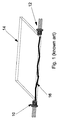
この種類の従来の接触パネルの構成原理と操作原理は、図1〜図3に示される。図1は、長方形の平面導波路14の反対の縁に位置する典型的なLED発光体10と光検出器12とを示す。この平面導波路は、通常、可塑性材料であり、前記材料は、空気との境界での合理的な入射角度に対する全内部反射に対応するように、その屈折率が十分に高いように選択される。その上、指の接触がこの全内部反射を乱し、導波路にわたる伝送を低減させるように選択される。光線16は、全内部反射により発光体10から検出器12に通過するように示されている。実際には、当然、導波路の縁に沿って複数の発光体10と検出器12があり、図2及び図3には簡略化のために、縁ごとに、それらのうちの4つのみが示され、光は、発光体から多数の交差する光学経路18を介して検出器で受光される。
The construction principle and operation principle of this type of conventional touch panel are shown in FIGS. FIG. 1 shows a
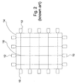
図2及び図3は、従来の配置を示し、各組の発光体10が導波路14の2つの隣接する縁に沿って配置され、各組の検出器12が他の2つの隣接する縁に沿って配置されることにより、各組の検出器は、導波路の反対の縁上で各組の発光体に向いている。この配置では、各検出器12は、その真反対の発光体10のみから光を受光するように配置され、それに対応して、各発光体10は、その直接的に反対の検出器12のみへ光を伝送するように配置される。このように、光学経路18は、交差する直交格子を形成し、光学経路間の交点に影響を与えるいずれかの所与の接触点のX−Y座標は、影響を受ける光学経路の特定の組み合わせにより定められ得る。
2 and 3 show a conventional arrangement, where each set of
発光体10と検出器12は、各々が、CPU20により駆動回路22と取得回路28を介して駆動され、CPUは、その上、アナログ・デジタル変換後に、受信された光データを処理し、接触点の場所を特定する役割をする。複数の発光体と検出器が導波路の縁に沿って配置されることにより、伝送損失に対して、数多くの交差する光学経路が測定され得る。これは、光学経路の密度が十分に高い場合、光学経路の交点での接触点が1つを超える光学経路に影響を与えるので、その接触点を極めて正確に特定することができることを意味する。光伝送データに補間を用いて、光線(発光体から検出器への直接経路)間の接触の位置を定めることができ、その接触領域は全てに及ぶ。
The illuminant 10 and the
更に、光線データを処理して、接触領域を推定することができ、その推定接触領域は、接触位置データを補足するのに、例えば、接触が事象を誘発するべきか否かを判定するのに利用され得る。システムの解像度と小さな接触領域の検出能は、主に、導波路の寸法、その厚さ、検出器の数、及び、A/D変換器に現れるような、発光体信号の信号対雑音比により定められる。導波路内に多くの光学経路があるので、1つを超える接触を個別に検出することができる。これには幾つかの用途があり、例えば、アルファベット・数字接触キーボード上に「シフト」機能を与える。 In addition, the ray data can be processed to estimate the touch area, which can be used to supplement the touch position data, for example, to determine whether touch should trigger an event. Can be used. The resolution of the system and the ability to detect small contact areas are mainly due to the size of the waveguide, its thickness, the number of detectors, and the signal-to-noise ratio of the illuminant signal as it appears in the A / D converter. Determined. Since there are many optical paths in the waveguide, more than one contact can be detected individually. This has several uses, for example, providing a “shift” function on an alphabetic / numeric touch keyboard.
光学経路が横切るそのようなパネルは、接触事象を検出することに加えて、光学経路に沿って配置される機械的制御デバイスの動作を検出することができる。例えば、機械的ボタン制御を光学経路に沿って挿入することができ、それにより、ボタン制御は、ボタン作動装置がその静止位置にあるときには、光エネルギーの減衰が最小であるが、ボタン作動装置が押されるときには、光が十分に減衰される。これは、ボタンが押されたときに光学経路内に不透明な羽板を導入することにより達成され得る。制御デバイスのための様々な機械的設計を利用して、光経路に沿って進む光エネルギーを変更することができるので、光学検出器からの信号を処理することにより、そのような制御デバイスの状態を検出することができる。 Such a panel traversed by the optical path can detect movement of a mechanical control device disposed along the optical path in addition to detecting a touch event. For example, a mechanical button control can be inserted along the optical path so that the button control has minimal attenuation of light energy when the button actuator is in its rest position, but the button actuator When pressed, the light is sufficiently attenuated. This can be achieved by introducing an opaque vane in the optical path when the button is pressed. Various mechanical designs for the control device can be used to change the light energy traveling along the light path, so that the state of such a control device can be determined by processing the signal from the optical detector. Can be detected.
広い領域にわたるセンシングを提供するために複数の発光体と複数の検出器を利用するようなパネルでは、発光体は、操作時に多大な電流を必要とし、高速応答に設定された検出器内を流れる光電流は、その上、かなりの量になり得る。これは、抵抗性接触センシング等の電力消費の僅かな他のセンシング技術とは対照的である。
本発明は、を目的とする。
In panels that utilize multiple light emitters and multiple detectors to provide sensing over a large area, the light emitters require significant current during operation and flow through detectors that are set for fast response. In addition, the photocurrent can be significant. This is in contrast to other sensing technologies that consume little power, such as resistive touch sensing.
The present invention is aimed at.
従って、本発明は、
複数の発光体、及び、複数の光検出器を含む1つの検出システムであって、前記発光体と前記光検出器がそれらの間に光経路の領域を定めることにより、発光体と検出器との間のエネルギーの伝送は、前記領域の近傍で生じる光学的相互作用により変調でき、前記検出システムが、1つ以上の前記光検出器の積算出力を経時的に与えるように操作され得る、複数の発光体及び検出システムと、
前記出力システムの動作を制御する切替手段と、
前記検出システムの出力を受信し、デジタル値に変換するアナログ・デジタル変換(ADC)手段と、
前記ADC手段からの前記デジタル値を受信し、その値に応答して前記切替手段を制御することにより、前記ADC手段の操作上の入力範囲に対応して、積算出力の遂次動作範囲を調節する、フィードバック機構と
以下を含む光制御システムを提供する。
Therefore, the present invention
A detection system including a plurality of light emitters and a plurality of light detectors, wherein the light emitter and the light detector define a region of an optical path between them, and the light emitter and the detector The transmission of energy between can be modulated by optical interactions that occur in the vicinity of the region, and the detection system can be operated to provide integrated output of one or more of the photodetectors over time. A light emitter and detection system of
Switching means for controlling the operation of the output system;
Analog-to-digital conversion (ADC) means for receiving the output of the detection system and converting it to a digital value;
By receiving the digital value from the ADC means and controlling the switching means in response to the value, the successive operation range of the integrated output is adjusted corresponding to the input range in operation of the ADC means. A light control system including a feedback mechanism and:
好ましくは、検出システムは、1つ以上の前記光検出器の出力を経時的に受信し、積算する積分器を含み、前記切替手段スイッチは、前記積分器及び/又はその関連検出器の動作を制御するように操作され得る。 Preferably, the detection system includes an integrator that receives and integrates the outputs of one or more of the photodetectors over time, and the switching means switch controls the operation of the integrator and / or its associated detector. Can be manipulated to control.
加えて又は代わりに、1つ以上の前記光検出器を比較的長い応答時間に設定することにより、前記1つ以上の前記光検出器は、積分器として作動する。 In addition or alternatively, by setting one or more of the photodetectors to a relatively long response time, the one or more of the photodetectors operate as an integrator.
フィードバック機構の目的は、積算出力の遂次動作範囲を、前記ADC手段の操作上の入力範囲に整合することにより、ADC手段の量子化雑音を最小限にすることである。 The purpose of the feedback mechanism is to minimize the quantization noise of the ADC means by matching the sequential operating range of the integrated output to the operational input range of the ADC means.
任意選択的に、フィードバック機構の目的は、所望の最小値を上回る前記ADC手段の出力で(又は、前記ADC手段からの測定値の処理内の後続の点で)、信号対雑音比を得ることにあり得る。 Optionally, the purpose of the feedback mechanism is to obtain a signal-to-noise ratio at the output of the ADC means above the desired minimum (or at a subsequent point in the processing of measurements from the ADC means). Can be.
これにより、通常、電力消費は最小限になる(積算時間が、適切な雑音性能に必要とされる最短のものになり、発光体が、積算時間に対してのみ作動状態であることを必要とするからである)が、信号対雑音比は、最適ではなく、妥当になる。 This usually minimizes power consumption (integration time is the shortest required for proper noise performance and requires that the illuminant be in operation only for the integration time. However, the signal-to-noise ratio is not optimal and is reasonable.
本明細事項において、用語「光」は、IR及びUV放射を含み、用語「光の」は、それに従って解釈されるものである。 In this specification, the term “light” includes IR and UV radiation, and the term “light” is to be interpreted accordingly.
好ましくは、システムは、前記積分器の作動周期の前に又はその間に、前記積分器に相殺電荷を与える補償回路を含み、それにより、前記相殺電荷は、前記1つ以上の前記光検出器から受信されるが、前記発光体の動作に関連していない背景信号を相殺するように働く。 Preferably, the system includes a compensation circuit that provides a canceling charge to the integrator prior to or during the operating period of the integrator, whereby the canceling charge is derived from the one or more of the photodetectors. It acts to cancel background signals that are received but not related to the operation of the light emitter.
更に、好ましくは、前記相殺電荷は、ADC手段からのデジタル出力値から導出され、前記出力値は、前記積分器に接続する前記1つ以上の検出器により受信されるエネルギーを伝送する発光体が作動状態ではないときに測定される。 Further preferably, the cancellation charge is derived from a digital output value from the ADC means, the output value being transmitted by an illuminant that transmits energy received by the one or more detectors connected to the integrator. Measured when not in operation.
任意選択的に、前記相殺電荷は、ADC手段からの最小デジタル出力値から導出され、前記出力値は、発光体が変調信号で駆動されているときに測定される。 Optionally, the cancellation charge is derived from a minimum digital output value from the ADC means, and the output value is measured when the light emitter is driven with a modulation signal.
システムは、積分器を制御可能に放電、帯電し、積算出力をデジタル形式に変換するために、前記積分器と前記ADC手段の動作を制御する制御器も含み得る。 The system may also include a controller that controls the operation of the integrator and the ADC means to controllably discharge and charge the integrator and convert the accumulated output to digital form.
好ましくは、前記積分器は、コンデンサを含み、前記コンデンサを制御可能に放電するために、前記制御器の制御下で前記コンデンサが選択的に接続され得る吸い込み装置を更に含む。 Preferably, the integrator includes a capacitor and further includes a suction device to which the capacitor can be selectively connected under control of the controller to controllably discharge the capacitor.
更に、好ましくは、前記制御器は、(i)前記コンデンサが前記吸い込み装置から隔離される帯電状態、(ii)前記コンデンサが前記ADC手段に接続される測定状態、及び(iii)前記コンデンサが前記吸い込み装置に接続される放電状態から選択される3つの状態うちの1つに、前記コンデンサと前記ADC手段と前記吸い込み装置との間の接続を再設定することにより、前記積分器と前記ADC手段とを制御するように作動する。 Further preferably, the controller is (i) a charged state in which the capacitor is isolated from the suction device, (ii) a measurement state in which the capacitor is connected to the ADC means, and (iii) the capacitor is in the Reconfiguring the connection between the capacitor, the ADC means and the suction device to one of three states selected from the discharge states connected to the suction device, thereby providing the integrator and the ADC means; And act to control.
任意選択的に、ADC手段は、アナログ出力ピンを備えたデバイスに組み込まれ、前記コンデンサは、前記アナログ出力ピンに接続され、前記アナログ出力ピンは、前記制御器の制御下で、前記3つの状態のうちの1つの状態を選択するように再設定され得る。 Optionally, the ADC means is incorporated in a device with an analog output pin, the capacitor is connected to the analog output pin, and the analog output pin is under the control of the controller and the three states Can be reset to select one of the states.
制御器は、更に、相殺電荷を前記コンデンサに与える前記補償回路に前記コンデンサが接続される、第4の状態を選択するように操作され得る。 The controller may be further operated to select a fourth state in which the capacitor is connected to the compensation circuit that provides a cancellation charge to the capacitor.
制御器は、代わりに又は追加的に、更に、保持状態を与えるために前記コンデンサが荷電経路と放電経路の両方から隔離される、第5の状態を選択するように操作され得る。 The controller may alternatively or additionally be further operated to select a fifth state in which the capacitor is isolated from both the charge path and the discharge path to provide a hold state.
好ましくは、システムは、1つ以上の前記発光体のための駆動回路を更に含み、前記駆動回路は、前記積分器及び/又はその関連検出器の前記作動時間未満のパルス周期で、前記1つ以上の前記発光体にパルスを発信させるように操作され得る。 Preferably, the system further comprises a drive circuit for one or more of the light emitters, wherein the drive circuit has the one cycle with a pulse period less than the operating time of the integrator and / or its associated detector. The above light emitter can be operated to emit a pulse.
検出器で受信され得る望まれない光エネルギーの量が比較的小さい場所では、発光体が常に作動状態であり得る間の極めて短い積算時間で、妥当な信号対雑音性能を得ることができる。制御器は、妥当な信号対雑音比をもたらす最小の時間尺度では積分器を操作することができ得ず、そのために、発光体は、必要以上に長く作動状態である場合があり、これは、エネルギーの浪費になる。この理由又は他の理由で、積算時間内に発光体使用率を調節することができることは、有利であり得る。 Where the amount of undesired light energy that can be received at the detector is relatively small, reasonable signal-to-noise performance can be obtained with a very short integration time while the light emitter can always be in operation. The controller cannot operate the integrator at the minimum time scale that results in a reasonable signal-to-noise ratio, so that the illuminator may be active longer than necessary, It is a waste of energy. For this reason or other reasons, it may be advantageous to be able to adjust the phosphor usage within the integration time.
駆動回路は、積分器の出力が発光体の使用率にほぼ比例するように、前記1つ以上の発光体の使用率を制御する手段を更に含み得る。 The drive circuit may further include means for controlling the utilization of the one or more light emitters such that the output of the integrator is approximately proportional to the utilization of the light emitter.
任意選択的に、光制御システムは、前記積分器の出力の信号対雑音比を定めて、前記信号対雑音比を既定の最小値によりも上に維持するように発光体使用率を制御する手段を更に含み得る。 Optionally, the light control system defines a signal-to-noise ratio at the output of the integrator and controls the light emitter usage rate so as to maintain the signal-to-noise ratio above a predetermined minimum value. May further be included.
好ましくは、前記駆動回路は、複数の前記発光体を制御するように、且つ、前記複数の発光体の作動が時間的にずれることを確保するように操作され得、それにより、いずれかの所与の時点で作動状態である発光体の数が削減される。更に、好ましくは、いずれかの所与の定数で作動状態である発光体の数は、最小限に削減される。 Preferably, the drive circuit is operable to control a plurality of the light emitters and to ensure that the operations of the plurality of light emitters are offset in time, thereby The number of light emitters that are active at a given time is reduced. Furthermore, preferably the number of illuminants that are active at any given constant is reduced to a minimum.
光経路の領域は、接触可能な表面の近くに位置し得るので、前記光相互作用は、接触可能な表面に触れることである。光経路の領域が、表面の近くの空隙又はいずれかの他の媒体内に与えられ得ることが理解されるであろう。 Since the region of the optical path can be located near the accessible surface, the optical interaction is to touch the accessible surface. It will be appreciated that the region of the light path can be provided in a void near the surface or any other medium.
好ましくは、接触可能な表面は、シート状導波路の表面であり、発光体と検出器は、光が発光体により導波路内に伝送され、導波路内の全内部反射により前記複数の交差する光経路に沿って検出器により受信されるように、導波路の縁に配置され、導波路の材料は、前記少なくとも2つの光経路に沿って進む光の量が、導波路の前記表面に触れて導波路から光を漏らすことを含む光相互作用により低減されるように選択される。 Preferably, the contactable surface is a surface of a sheet-like waveguide, and the light emitter and the detector are such that light is transmitted into the waveguide by the light emitter and the plurality of intersections by total internal reflection in the waveguide. Located at the edge of the waveguide so that it is received by the detector along the optical path, the material of the waveguide is such that the amount of light traveling along the at least two optical paths touches the surface of the waveguide. And selected to be reduced by light interaction including leakage of light from the waveguide.
好ましくは、前記ADC手段は、複数の前記検出器からの複数の多重化信号を受信する。 Preferably, the ADC means receives a plurality of multiplexed signals from a plurality of the detectors.
好ましくは、検出器の作動時間を制御する切替手段は、前記検出器により検出される信号の振幅に応じて調節され得る。 Preferably, the switching means for controlling the operation time of the detector can be adjusted according to the amplitude of the signal detected by the detector.
システムは、前記ADC手段の動作を制御し、前記積分器の積算時間の間に前記積分器の出力の信号を抽出し、前記信号抽出から、前記積算時間の終端での推定最終積分器出力を推定するためのプロセッサを更に含み得る。 The system controls the operation of the ADC means, extracts a signal of the integrator output during the integration time of the integrator, and calculates an estimated final integrator output at the end of the integration time from the signal extraction. A processor for estimating may further be included.
好ましくは、前記プロセッサは、前記推定最終積分器出力が、前記ADC手段の操作上の入力限界を超えそうであるか判定し、もしそうであれば、積算時間を削減するように操作され得る。 Preferably, the processor determines whether the estimated final integrator output is likely to exceed an operational input limit of the ADC means, and if so, may be operated to reduce integration time.
更に、好ましくは、前記プロセッサは、前記抽出された積分器出力の補間を実行し、前記ADC手段の前記操作上の限界を超えると思われる飽和時間を定め、前記削減される積算時間を、前記飽和時間以下の値に設定する。 Further preferably, the processor performs an interpolation of the extracted integrator output to determine a saturation time that is likely to exceed the operational limit of the ADC means, and to reduce the accumulated time, Set to a value less than the saturation time.
任意選択的に、前記プロセッサは、前記推定最終積分器出力が、前記ADC手段の操作上の入力限界を超えそうであるか判定し、もしそうであれば、飽和ADC出力に代わる出力として、前記推定最終積分器出力を供給するように操作され得る。 Optionally, the processor determines whether the estimated final integrator output is likely to exceed an operational input limit of the ADC means, and if so, as an output to replace a saturated ADC output, It can be operated to provide an estimated final integrator output.
本発明は、
複数の発光体から複数の光検出器へエネルギーを伝送する工程であって、前記発光体及び検出器がそれらの間に光経路の領域を定めることにより、発光体と検出器との間のエネルギーの伝送が、前記領域の近傍で生じる光相互作用により変調され得る、エネルギー伝送工程と、
積分器で1つ以上の前記光検出器の出力を受信し、出力信号を経時的に積算する工程と、
前記積分器及び/又はその1つ以上の検出器の作動時間を制御する工程と、
アナログ・デジタル変換器(ADC)手段を利用して、前記積分器から積算出力信号を受信し、前記積算出力信号をデジタル値に変換する工程と、
前記デジタル値に応答して切替手段を制御することにより、前記ADC手段の操作上の入力範囲に対応して、積分器出力の随時動作範囲を調節する工程と
を含む光制御システムを操作する方法も提供する。
The present invention
Transferring energy from a plurality of light emitters to a plurality of light detectors, wherein the light emitter and the detector define a region of a light path between them, whereby the energy between the light emitter and the detector. Energy transmission process, wherein the transmission of can be modulated by optical interactions occurring in the vicinity of the region;
Receiving an output of one or more photodetectors with an integrator and integrating the output signal over time;
Controlling the operating time of the integrator and / or one or more detectors thereof;
Using an analog-to-digital converter (ADC) means to receive an integrated output signal from the integrator and convert the integrated output signal to a digital value;
Adjusting the operating range of the integrator output at any time corresponding to the operational input range of the ADC means by controlling the switching means in response to the digital value. Also provide.
好ましくは、前記制御工程は、前記ADC手段の操作上の入力範囲に対応して積分器出力の範囲を調節し、最低値を上回る信号対雑音比を得ることを含む。 Preferably, the control step includes adjusting an integrator output range corresponding to an operational input range of the ADC means to obtain a signal-to-noise ratio exceeding a minimum value.
別の独立した態様では、本発明は、
複数の発光体と複数の光検出器であって、それらの間に光経路の領域を定めることにより、発光体と検出器との間のエネルギーの伝送が、前記領域の近傍で生じる光相互作用により変調され得る、複数の発光体及び検出器と、
1つ以上の前記光検出器の出力を経時的に受信し、積算する積分器と、
前記積分器の出力を受信し、デジタル値に変換するアナログ・デジタル変換器(ADC)手段と、
前記積分器の作動周期の前に又はその間に、相殺電荷を前記積分器に与える補償回路であって、それにより、前記相殺電荷が、前記1つ以上の前記光検出器から受信されるが前記発光体の動作に関連していない背景信号を相殺するように働く、補償回路と
を含む光制御システムを提供する。
In another independent aspect, the present invention provides:
A plurality of light emitters and a plurality of light detectors, wherein a light path region between them defines a light interaction between the light emitter and the detector that occurs in the vicinity of the region; A plurality of emitters and detectors that can be modulated by:
An integrator for receiving and integrating the output of one or more of said photodetectors over time;
Analog-to-digital converter (ADC) means for receiving the output of the integrator and converting it to a digital value;
A compensation circuit that provides a canceling charge to the integrator before or during an operating period of the integrator, whereby the canceling charge is received from the one or more photodetectors. A light control system is provided that includes a compensation circuit that serves to cancel background signals not related to the operation of the light emitter.
更なる独立した態様では、本発明は、
複数の発光体と複数の光検出器であって、それらの間に光経路の領域を定めることにより、発光体と検出器との間でのエネルギーの伝送が、前記領域の近傍で生じる光相互作用により変調され得る、複数の発光体及び光検出器と、
既定の積算時間にわたり1つ以上の前記光検出器の出力を受信し、積算する積分器と、
前記積分器の出力を受信し、デジタル値に変換するアナログ・デジタル変換器(ADC)手段と、
前記ADC手段の動作を制御し、前記積分器の前記積算時間の間に前記積分器出力の信号を抽出し、前記信号抽出から、前記積算時間の終端での、推定最終積分器出力を推定するプロセッサと
を含む光制御システムを提供する。
In a further independent aspect, the present invention provides:
A plurality of light emitters and a plurality of light detectors, wherein an optical path region is defined between the light emitters and the light detectors so that energy transfer between the light emitters and the detectors occurs in the vicinity of the region. A plurality of light emitters and photodetectors that can be modulated by action;
An integrator for receiving and integrating the output of one or more of the photodetectors over a predetermined integration time;
Analog-to-digital converter (ADC) means for receiving the output of the integrator and converting it to a digital value;
Control the operation of the ADC means, extract the integrator output signal during the integration time of the integrator, and estimate the estimated final integrator output at the end of the integration time from the signal extraction A light control system including a processor is provided.
好ましくは、前記プロセッサは、前記推定最終積分器出力が、前記ADC手段の操作上の入力限界を超えそうであるか判定し、もしそうであれば、積算時間を削減するように操作され得る。 Preferably, the processor determines whether the estimated final integrator output is likely to exceed an operational input limit of the ADC means, and if so, may be operated to reduce integration time.
任意選択的に、前記プロセッサは、前記推定最終積分器出力が、前記ADC手段の操作上の入力限界を超えそうであるか判定し、もしそうであれば、飽和ADC出力に代わる出力として、前記推定最終積分器出力を供給するように操作され得る。 Optionally, the processor determines whether the estimated final integrator output is likely to exceed an operational input limit of the ADC means, and if so, as an output to replace a saturated ADC output, It can be operated to provide an estimated final integrator output.
別の独立した態様では、
複数の発光体と複数の光検出器であって、それらの間に光経路の領域を定めることにより、発光体と検出器との間のエネルギーの伝送が、前記領域の近傍で生じる光相互作用により変調され得る、複数の発光体及び光検出器と、
1つ以上の前記光検出器から信号を受信し、その信号から導出された信号値をデジタルの形態で与える回路と、
前記導出された信号値を受信するプロセッサであって、前記プロセッサは、前記導出された信号値から前記検出器の信号対雑音比を定め、前記信号対雑音比を既定の最小値よりも上に維持するために発光体出力を制御するように操作され得る、プロセッサと
を含む光制御システムが提供される。
In another independent aspect,
A plurality of light emitters and a plurality of light detectors, wherein a light path region between them defines a light interaction between the light emitter and the detector that occurs in the vicinity of the region; A plurality of light emitters and photodetectors that can be modulated by:
A circuit for receiving a signal from one or more of the photodetectors and providing a signal value derived from the signal in digital form;
A processor for receiving the derived signal value, the processor determining a signal-to-noise ratio of the detector from the derived signal value and bringing the signal-to-noise ratio above a predetermined minimum value. A light control system is provided that includes a processor that can be operated to control the light emitter output to maintain.
本発明の実施形態は、ここで、例として、付属の図面を参照しながら記載されることになる。 Embodiments of the invention will now be described by way of example with reference to the accompanying drawings.
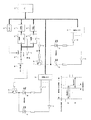
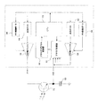
本発明の実施形態は、図3の接触パネルの発光体駆動装置22及び検出器信号調節・変換回路24に関連する。一実施形態は、光トランジスタ及びフォトダーリントン等の高利得の光検出器が、通常、LED等の発光体よりも極めて低速動作であることに基づいているので、放射エネルギーを受信する検出器の応答時間内で発光体が作動状態であるように、極めて高速に発光体をパルス発信させることができる。発光体の作動周期が長ければ、検出器の出力で受信される信号は長くなる。実際に、検出器を利用して、発光体からエネルギーを経時的に積分することができる。コンデンサ等の追加の部品は、積分電荷累算器として働くように追加され得る。発光体作動周期を制御するためにデジタル回路に必要なクロック速度は、標準のデジタルデバイスの範囲内で十分である。
Embodiments of the present invention relate to the touch panel
発光体自体の熱容量により、その発光体が過剰に加熱されるのを防止することができる。これは、従来の駆動回路内で、通常、発光体に直列に与えられる抵抗を総計で極めて多く削減又は除去することができ、その結果生じる、直列抵抗を加熱する無駄なエネルギーの分散を削減又は回避することができることを意味する。 The heat capacity of the light emitter itself can prevent the light emitter from being heated excessively. This can significantly reduce or eliminate, in total, the resistance typically provided in series with the light emitter within a conventional drive circuit, resulting in a reduction in the wasteful energy distribution that heats the series resistance or It means that it can be avoided.
ソフトウェア制御下の極高速のマイクロプロセッサは、発光体を断続的に駆動するのに必要とされる時間調節パターンを生成し得るが、多くの場合、プロセッサは、必要とされる性能を有していないか、又は、これは、CPU時間の利用が乏しいことになる。従って、本実施形態では、必要とされる時間調節は、複数の発光体を群で又は個別に駆動するのに容易に拡張される、図4の比較的簡易な回路で生成される。 Extremely fast microprocessors under software control can produce the time adjustment pattern required to drive the light emitter intermittently, but in many cases the processor has the required performance. There is no or less CPU time utilization. Thus, in this embodiment, the required time adjustment is generated with the relatively simple circuit of FIG. 4 that is easily extended to drive multiple light emitters in groups or individually.
図4を参照して、CPU20は、対応するレジスタ28に、第1群の発光体26の所望の「オン」の継続時間又は作動周期に対応する値を書き込む。値は、クロックパルス生成器30のクロックパルスの数に特定される。第2群の発光体34に対応するレジスタ32がある。ソフトウェアが、発光体26及び34の作動周期が開始するべきであると判定するときに、CPU20は、対応する発光体は作動することになるように、出力レジスタ35及び38のそれらのビットに「1」値を書き込み、クロック発生器30からのパルスを零から計数し始めることができるように、カウンタ42上の同期再設定線を解除する出力ポートビット40に「0」値を書き込む。レジスタ36及び38の出力は、発光体駆動装置44により反転され、それぞれに共通の陽極駆動トランジスタ46及び48が切り替えられるときに、発光体26及び34の陰極からの電流を吸い込む。レジスタ28内の全ての非ゼロ値に対して、振幅比較器のA<B出力は、カウンタ42が再び開始するときに高になるので、反転バッファ52の出力は、低になり、発光体駆動器トランジスタ46は、オンにされる。カウンタ42の出力がレジスタ28内の値に等しくなるときに、振幅比較器50のA<B出力は低になり、発光体26への駆動は取り除かれ、その発光体はオフにされる。カウンタ42は、その最大値に達するまで計数し続け、その値で、ゼロ値で再び開始する。このように、レジスタ28に書き込まれる値は、全サイクル周期内に発光体26の作動又はオン周期を定める。
Referring to FIG. 4,
レジスタ32内の値をカウンタ42の出力と比較する第2比較器54は、第2群の発光体34に対して設けられる。比較器54の出力は、反転バッファ56により反転され、カウンタ42がレジスタ32内の値以上の出力を有するときに、トランジスタ48をオンにする。
A
例えば、4ビットカウンタ42が利用され、10クロックパルスの継続時間にわたって発光体26をオンにし、8クロックパルスの継続時間にわたって別の発光体34をオンにすることが望まれる場合、CPUは、初期に、レジスタ28に「1010」(10の二値)を書き込み、レジスタ32に「0111」(7の二値)を書き込む。発光体作動周期を開始するのが望まれる場合、昇りエッジが、カウンタ42の再設定ピンに送られ、前記カウンタは、クロックパルス生成器30からのクロックパルスを計数することができる。カウンタは、その計数を「0000」に初期化し、クロックパルス生成器30からのクロックパルス毎に1だけ増分する。比較器50は、カウンタの出力を、レジスタ28の格納された値と比較する。カウンタ出力が「1010」未満であるときに、「A<B」と記されたピンは、高のままであり、その状態は、バッファ52への入力で反転され、トランジスタ46は、発光体26に電流を供給し、いずれかの発光体をオンにし、それに対して、レジスタ36内は1である。カウンタが「1010」のカウントに達した後に、「A<B」は、低になり、トランジスタ46をオフにする。そのトランジスタがオフの間、電流は供給されず、発光体26は、全てオフになる。
For example, if a 4-
反対に、比較器54上の「A>B」と記されるピンは、低のままであるのに対し、カウンタ出力は、「0111」以下であり、それは、クロックパルス生成器30の最初の8周期にわたり、トランジスタ48をオフにする。トランジスタ48は、発光体34に電流を供給し、それらの発光体の全ては、「A>B」と記されるピンが高になるまで、オフにされることになる。これは、カウンタ42の出力値が「1000」に達するときに起こり、そのとき、トランジスタ48は、バッファ56の反転動作を通じてオンにされ、レジスタ38内で1ビットである、あらゆる発光体をオンにする。
Conversely, the pin marked “A> B” on the
この実施形態により、レジスタ28内に選択されるカウントを設定することにより、発光体26の作動周期の継続時間を調節することができ、並びに、レジスタ32内に選択されるカウントを設定することにより、発光体34を同様に制御することができる。
According to this embodiment, by setting the count selected in the
発光体26の群と発光体34の群は、同時に作動状態であり得るが、重なり合いの継続時間は、最小限に保たれる。 The group of illuminants 26 and the group of illuminants 34 can be active at the same time, but the overlap duration is kept to a minimum.
図4は、2つの群の発光体26及び34のみに対する駆動回路を示すけれども、任意の追加の発光体群に対する類似の駆動回路があり得、それらの群に対しては、個別の電源制御が設けられることになる。クロックパルス生成器30とカウンタ42は、全ての発光体群に共通するが、その群内の発光体使用率を制御するために、各発光体群に対する個別の比較器及びレジスタを必要とし得る。
Although FIG. 4 shows drive circuits for only two groups of light emitters 26 and 34, there may be similar drive circuits for any additional light emitter groups, for which individual power control is provided. Will be provided. The
発光体の作動は、市販のマイクロプロセッサ上のパルス幅変調ユニットを利用して達成され得る。 The operation of the light emitter can be accomplished using a pulse width modulation unit on a commercially available microprocessor.
関連する原理を検出器12に適用して、限定された時間周期にわたり検出器を作動させることにより、光電流が流れる時間を制御することができる。
By applying the relevant principle to the
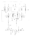
アナログ検出器出力データを、CPU20により処理するためのデジタル形式に変換するのに利用されるアナログ・デジタル(A/D)変換器の数は、多数の検出器出力を単一のA/D変換器に重ねることにより削減され得る。変換器の所与の速度に対して、これにより、全ての検出器出力を変換する時間が増加することになる。検出器出力を捕獲して、変換の間に発光体出力を取り除くことができ、これを行う従来の方法は、信号抽出・保持回路を利用し、検出される光エネルギーレベルをコンデンサ内で保持することであった。変換時間の間に発光体をオフにすることにより、全ての電力消費は削減される。通常の実施は、検出器出力を保持コンデンサに接続するためにアナログ切替器を利用し、光電流を電圧に変換するためにレジスタを利用していた。図5は、そのような従来の機構の実施例を示す。レジスタ58は、検出器60からの電流を、相当する電圧に変換していた。検出器作動周期の間に、マイクロプロセッサCPU62は、保持コンデンサ66が、抵抗58にわたって検出された電圧を追跡するように、アナログ切替器64を閉じた状態に保っていた。CPU62は、1ビット二値制御値を出力ポート68に書き込むことによりアナログ切替器64を制御していた。検出器作動周期の終端では、CPU62は、保持コンデンサ66が最終的に検出された電圧を保つように、アナログ切替器64を開いていた。CPU62は、複数の検出器により検出された電圧が、単一のアナログ・デジタル変換器72によりデジタル値に変換され得るように、アナログ多重器70を制御していた。デジタル変換が完了したときに、保持コンデンサ66は、CPU62により出力ポート76を介して制御されるアナログ切替器74を通じて放電されていた。アナログ切替器74は、次の抽出操作の前に、再び開かれていた。
The number of analog-to-digital (A / D) converters used to convert the analog detector output data into a digital format for processing by the
しかしながら、図6の本実施形態では、検出回路は、3状態論理出力バッファ76を利用して、検出器78を駆動することにより簡略化され、検出器は、発光体がオフにされた場合、高インピーダンス状態に置かれ得る。コンデンサ80は、次に、検出器出力に直接接続され、検出器出力電圧を保持するために利用され得る。
However, in the present embodiment of FIG. 6, the detection circuit is simplified by driving a
検出器作動周期の間に、CPU82は、出力ポート84を高レベルに設定することにより、且つ、対応するピン制御ポート86を設定することにより、節点Aでの検出器78に電流を供給し、3状態出力バッファ76を有効化する。コンデンサ80は、検出器78を通る光電流により定められる割合で帯電され、光電流は、検出器で入射される光エネルギーに依存する。コンデンサ80は、この時間の間は、実質的に積分コンデンサである。検出器作動周期の終端に、CPU82は、ピン制御ポート86を、3状態出力バッファ76を無効にするように設定することにより電流源を取り除き、そのバッファを高インピーダンス状態にする。これにより、検出器はオフにされる。点Bでのコンデンサ80上に存在する電圧は、光電流と、電流源が利用された時間周期により定められる。主に、点Bに接続されるマイクロコントローラピンを通じてのコンデンサ80上の電荷の漏れがあるが、容量値は、変換が実行される時間の間、電圧降下がアナログ・デジタル変換器88の精度内にあるように選択され得る。
During the detector operating cycle, the
不完全なサイクルは、発光体のパルス継続時間とコンデンサ80上の累積された検出器値との間の関係の線形性を低減するので、好ましくは、検出器78の作動又は「オン」周期の継続時間は、発光体の作動周期の整数である。この非線形性は、検出器作動時間の間の発光体サイクル数が増加するにつれて、あまり重要ではなくなる。
Incomplete cycles preferably reduce the linearity of the relationship between the emitter pulse duration and the accumulated detector value on
図6に見られるように、点Bでの電圧は、複数の検出器78の各点Bに接続される複数の入力を有するアナログ多重器90の1つの入力に接続される。これらの入力は、対応する複数のコンデンサ80上のアナログ電圧がA/D変換器88により順番に変換されるように、CPU82により順番に有効にされる。
As seen in FIG. 6, the voltage at point B is connected to one input of an
検出器78のA/D変換プロセスが完了するとき、コンデンサ80は、出力ポート92を低条件に設定し、ピン制御ポート96を利用して別の3状態バッファ94を有効にすることにより放電される。コンデンサ80は、通常、小さな容量値を有し、3状態バッファ94は、通常、十分な電流吸い込み容量を有するので、放電時間は短くなる。3状態出力94は、検出時間及び変換時間の間にCPU82により無効にされるので、光電流測定を乱さない。
When the A / D conversion process of
検出器78の遂次動作範囲は、CPU82によりソフトウェア制御下で調節することができ、前記CPUは、電流が3状態バッファ76から供給される時間周期を変更する。フィードバックを与えるために、アナログ・デジタル変換器88の出力値を利用する。検出器78からのデジタル値が、アナログ・デジタル変換器88から入手可能な上限に近づくと、3状態バッファ76の作動周期は低減され、故に、コンデンサ80の帯電周期と、その結果生じる、アナログ多重器90を介してアナログ・デジタル変換器88に存在する電圧は削減される。
The sequential operating range of the
反対に、連続した組の測定にわたり生成される最大デジタル値がアナログ・デジタル変換器88の範囲内で高くない場合、3状態バッファ76の作動周期は増し、コンデンサ80上の電圧は高くなり、変換分解能は高くなり、その結果、量子化雑音は削減される。CPU82は、連続測定でデジタル値を処理し、所望の信号に対する望まれない雑音の比(例えば、外部雑音及びシステム雑音)を定めることができる。3状態バッファ76の作動周期は、この信号対雑音比が既定の最小値を上回るまで、CPU82の制御下で増す。
Conversely, if the maximum digital value generated over a continuous set of measurements is not high within the analog-to-
反対に、信号対雑音比が十分な差だけ最小要求量を超える場合、3状態バッファ76の作動周期は、CPU82の制御下で低減され得る。これにより閉ループ検出プロセスが導かれることで、検出時間は、許容可能な信号対雑音性能を与えるように変更される。3状態バッファ76が作動状態でないとすぐに発光体を無効にすることができるので、発光体の作動周期と関連する電流消費は最小になる。
Conversely, if the signal to noise ratio exceeds the minimum requirement by a sufficient difference, the operating period of the
3状態バッファ76の作動周期が、CPU82及び関連する抽出システムにより維持され得る最小値である場合でさえ、ADC88からの受信値を更に処理することで、信号対雑音比が、要求される最小値をまだ十分に上回っていることを明らかにすることができ、全てのシステム性能を著しく劣らせることなく、発光体出力電力を自動的に減少させることができる。
Further processing of the received value from the
周囲光レベルのみではなく、信号対雑音比に基づいて発光体出力を制御する考えは、(記載された、積分器を含むシステムばかりでなく)他の種類の検出システムにも適用され得る。あらゆる光検出システムにおいて、システム内の電力線の雑音のような、周囲光とは別の他の雑音源があり得る。信号対雑音比を計算し、それを発光体出力の基礎とすることにより、全ての雑音源を含めて、発光体出力を適切に設定することができる。 The idea of controlling the emitter output based not only on the ambient light level but also on the signal-to-noise ratio can be applied to other types of detection systems (as well as described systems including integrators). In any light detection system, there may be other noise sources apart from ambient light, such as power line noise in the system. By calculating the signal-to-noise ratio and using it as the basis for the emitter output, the emitter output can be set appropriately, including all noise sources.
例えば、光センシングが移動電話に利用される場合、検出器からADCピンまでのPCB経路内へのRFの入射は、電話呼び出しの間に著しく上昇し得、周囲光レベルは変化し得ないが、処理の出力での信号対雑音比は下がることになる。この降下は、発光体出力を増すことにより相殺され得る。発光体使用率は、積分検出器を用いて発光体出力を制御する好ましい方法であるが、電流制御が、非積算型検出システムを用いて利用され得る。 For example, if optical sensing is utilized in a mobile phone, the incidence of RF into the PCB path from the detector to the ADC pin can rise significantly during a phone call and the ambient light level cannot change, The signal to noise ratio at the output of the process will decrease. This drop can be offset by increasing the emitter output. While illuminant usage is a preferred method of controlling illuminant output using an integral detector, current control can be utilized using a non-integrating detection system.
本発明の更なる実施形態では、積分器として働くように応答時間が十分に長い検出器が、例えば、積分器として働くように十分な容量を備えた検出器が利用され得ることが理解されるであろう。 In further embodiments of the present invention, it will be appreciated that a detector with a sufficiently long response time to act as an integrator may be utilized, for example, a detector with sufficient capacity to act as an integrator. Will.
光トランジスタは、入射光のためのかなり大きな的を有するために、大きなベース領域を有する傾向にある。これより、コレクタ・ベース間接合容量は、通常、普通のトランジスタの容量よりもかなり大きく、通常、デバイスの応答時間を限定する要因である。検出器78が、光トランジスタである場合、真性容量は、本発明では積分要素として利用され得る。
Phototransistors tend to have a large base area in order to have a fairly large target for incident light. Thus, the collector-base junction capacitance is usually much larger than that of a normal transistor, and is usually a factor limiting the device response time. If the
CPU82は、節点Aを高レベルに移し、節点Bを低レベルに移すことにより、光トランジスタ78を放電することができる。節点Aでの高レベルは、二値の1値を出力ポート84に書き込み、二値の1値をピン制御ポート86に書き込み、出力バッファ76の出力を高状態に移すことにより得られる。節点Bでの低レベルは、二値の0値を出力ポート92に書き込み、高レベルをピン制御ポート96に書き込むことにより得られる。光トランジスタ78のコレクタ・ベース間接合の任意の電荷により、電流は、節点Aと節点Bとの間を流れることになり、これにより、光トランジスタ78のコレクタ・ベース間接合は放電される。
The
CPU82は、節点Aが高インピーダンス状態に設定されるように二値の0値をピン制御ポート86に書き込むことにより、光トランジスタ78が入射光を積算するように設定することができる。節点Bは、通常、低レベルのままである。入射光は、光トランジスタ78がこのモードである間、前記光トランジスタのコレクタ・ベース間領域を帯電することになる。
The
積分周期が終わったときに、CPU82は、二値の0値をピン制御ポート96に書き込み、前記ポートは、3状態バッファ94の出力を高インピーダンス状態に設定する。CPU82は、二値の1値をピン制御ポート86に書き込み、前記ポートは、二値の1値が出力ポート84内に保たれていると仮定して、3状態バッファ76の出力を高レベルに設定する。これにより、光トランジスタ78の電流源が与えられるので、光トランジスタ78のコレクタ・ベース間接合の任意の電荷により、コンデンサ80を帯電する電流が生じる。コンデンサ80上の電荷は、光トランジスタのコレクタ・ベース間接合上に累積された電荷と光トランジスタ78の利得との積である。
When the integration period ends, the
この帯電プロセスが完了したときに、CPU82は、二値の0値をピン制御ポート86に書き込むことにより、節点Aを高インピーダンス状態に設定する。コンデンサ80は、次に、最小限の漏れで電荷を保つ保持状態であるので、その結果得られるコンデンサ80上の電圧は、アナログ多重器90を介してADC88に現れ得る。
When this charging process is completed, the
保持モードが必要とされない場合、コンデンサ80を抵抗に入れ替え得るので、光トランジスタ78のコレクタ・ベース間接合上に累積された電荷は、前記レジスタ内に一時的な電流(再び、光トランジスタ78の電荷量と利得との積)を発生させ、節点Bでその結果生じる電圧は、アナログ多重器90を介してADC88により取得され得る。
If the holding mode is not required, the
本発明の追加の態様では、ADC88は、ソフトウェアにより指示されるような積分周期の間に堆積された電荷を抽出し得るので、コンデンサ80の帯電率を推定することができる。積分周期の終端に堆積された電荷がADC88の入力を飽和する程に、帯電率が高い場合、推定された帯電率を利用して、積分周期が削減されるべきである尤もらしい量を定め、次の積分結果をADCの入力範囲内に持って行くことができる。推定された帯電率を利用して、飽和されるADC信号抽出値に代わり得る信号抽出値を補間することもできる。
In an additional aspect of the invention, the
図7に見られるように、検出器電流節点Aを利用して、1つを超える検出器78に電流を与えることができる、即ち、点Cは、複数の検出器78のコレクタピンに接続されている。マイクロプロセッサデバイス上の出力パッドは、通常、限定された電流源容量を有するので、外部電流増幅を利用して、利用可能な電流を増すことができ、例えば、そのベースが抵抗100を介して3状態バッファ76の出力により制御される、2極トランジスタ98である。この場合、出力バッファ76は、検出器78が非作動状態にされるときにトランジスタ98が完全にオフであることを確保するのに十分な高い出力電圧を生成する能力がある場合、3状態型のバッファである必要はない。CPUは、トランジスタ98をオンにするために出力ポート84に「0」を書き込むことを必要とする。
As can be seen in FIG. 7, the detector current node A can be used to provide current to more than one
図7は、その上、検出器78に接続するダイオード102の光学的利用を示し、前記ダイオードを利用して、オフにされ得る共通の電力接続に検出器が接続されるときに、検出器間の漏れ電流を削減することができる。
FIG. 7 additionally shows the optical utilization of the
このように単一の出力ピンを共有することにより、複数の検出器に対応するのに必要とされるマイクロコントローラピンの数は削減されるが、それは、各検出器78に対する作動周期が同じになる、つまり、点Cに接続される各検出器が、そのコレクタ・エミッタ端子にわたる電圧を同時に受信することを意味するものではない。積算時間は、ソフトウェアで、ADC88に、個別に特定された積算周期の後にアナログ多重器90により選択されるような各コンデンサ80上で変換を実行するように指示することにより、個別に制御され得る。
Sharing a single output pin in this way reduces the number of microcontroller pins required to accommodate multiple detectors, but with the same operating period for each
測定は、通常、周囲光が導波路内と検出器内に入るのを限定するように行われる。これらの測定は、例えば、発光体と検出器との間の意図された経路に沿った光以外の光の通過を制限する不透明な覆いの形態を取り得る。しかしながら、ある量の周囲光が検出器に存在することは普通であり、これにより、実質的に一定な又は変調された偏差が、検出器出力に存在することになる。この偏差は、多くの場合、発光体からの信号と同じ大きさの振幅であり、ADCの入力範囲の利用を悪くする。 Measurements are usually made to limit ambient light from entering the waveguide and the detector. These measurements may take the form of an opaque covering that limits the passage of light other than light along the intended path between the emitter and detector, for example. However, it is common for a certain amount of ambient light to be present at the detector, so that a substantially constant or modulated deviation will be present at the detector output. This deviation is often of the same magnitude as the signal from the light emitter, making the ADC's input range poorly utilized.
偏差信号を最小限にするために様々な手段が開示されてきており、例えば、米国特許第4,684,801号(カロールら、1987年)では、作動状態の発光体で抽出された検出器出力信号レベルから、作動していない発光体で抽出された周囲の検出器出力レベルを引くための信号抽出・保持回路とプログラム可能な差分増幅器の利用が、開示されている。 Various means have been disclosed to minimize the deviation signal, for example, in US Pat. No. 4,684,801 (Karol et al., 1987), a detector extracted with an activated illuminant. The use of a signal extraction and hold circuit and a programmable difference amplifier to subtract the ambient detector output level extracted with an inactive illuminant from the output signal level is disclosed.
本発明の別の態様では、偏差は、ソフトウェア制御下で、偏差の大きさに対応するが極性が反対の電荷を積分コンデンサに事前に堆積させることにより取り除かれ得る。検出器が作動状態である間、その出力の偏差成分は、この帯電を中和し、コンデンサ上の残留電荷は、偏差相殺電荷と、検出器上に入射されるエネルギー、主に、発光体からの所望のエネルギーとの間の差を表す。 In another aspect of the invention, the deviation can be removed by predepositing an integrating capacitor under software control that corresponds to the magnitude of the deviation but of the opposite polarity. While the detector is active, the deviation component of its output neutralizes this charge, and the residual charge on the capacitor is the deviation cancellation charge and the energy incident on the detector, mainly from the light emitter. Represents the difference between the desired energy of
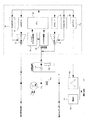
図8は、本発明の偏差打ち消しの態様の好ましい実施形態を示す。節点X,Y及びZは、様々な段階の信号抽出工程を制御する。最初に、積分コンデンサ104が、節点Y及びZを0Vに移すことにより放電され、節点Xは、同じ電位にあるか、又は、高インピーダンス状態にある。コンデンサ104は、次に、偏差を補償する事前の帯電で、抵抗又は電流源106等の電流制限デバイスを介して節点Zに正の電圧を加える一方で、節点Yを零電位で又はその近くに保つことによりで帯電される。帯電電流は、アナログ選択器108又は他の適切な切替手段を利用して、節点Zに制御可能に加えられ得る。帯電電流スイッチは、CPU82により、出力ポート110に書き込むことにより制御される。帯電時間の継続時間は、その結果生じる、コンデンサ104上の事前電荷を定める。検出及び積分工程では、前述のように、節点Xは、コンデンサ104を帯電させる検出器112を作動させるために、正の電位に引き上げられ、節点Zは、零電位にされ、節点Yは、高インピーダンス状態にされる。特定の積算時間の後に、マイクロコントローラADCへのアナログ入力になるように節点Yを切り替えることにより、コンデンサ104上の電圧の信号を抽出することができる。その結果生じる信号抽出値は、偏差事前電荷が中性にされた後にコンデンサ104内に蓄積される電荷に対応する。
FIG. 8 shows a preferred embodiment of the deviation cancellation aspect of the present invention. Nodes X, Y and Z control the various stages of signal extraction process. Initially, integrating
コンデンサ104の偏差事前電荷は、ソフトウェア制御下で、節点Yが零電位である一方で事前帯電電流が節点Zに加えられる時間周期を変調するCPU82により調節され得る。検出器112からのデジタル値が、アナログ・デジタル変換器88から入手可能な下位限界に近づくと、ノードYの作動周期は増し、故に、コンデンサ104の帯電周期は増し、その結果生じる事前電荷の大きさは、検出器112の出力の偏差成分により中性にされる。反対に、測定値が、アナログ・デジタル変換器88の範囲内で極めて低い場合、偏差事前電荷は、あまりにも大きく、節点Yの作動周期は減少し、コンデンサ104上の事前電荷は小さくなる。
The deviation pre-charge of the
節点X及びZは、幾つかの検出器とそれらの各々の積分コンデンサで共通し得る。図8に示される構成には、各検出器に対して1つのマイクロプロセッサピンしか必要とされないという特別の利点がある。 Nodes X and Z may be common to several detectors and their respective integrating capacitors. The configuration shown in FIG. 8 has the particular advantage that only one microprocessor pin is required for each detector.
任意選択的に、ダイオード114と抵抗116をADC入力に付け加えて、事前帯電操作の結果、節点Y上に別の場合に存在し得る負の電圧からそのADCを保護することができる。これらの部品が付け加えられる場合、コンデンサ104の事前帯電は、節点Yを高インピーダンス状態に設定するのではなく、節点Yを節点Xと同じ電位に移すことにより停止される。
Optionally,
積分コンデンサに反対の電荷を事前に堆積させることにより偏差を補償するこの方法は、例えば、演算増幅器を基調とした積分器等の他の実施形態にも有利に適用することができる。 This method of compensating for the deviation by pre-depositing the opposite charge on the integrating capacitor can also be advantageously applied to other embodiments such as, for example, an integrator based on an operational amplifier.
従って、本発明は、最小限の電子部品で発光体出力、検出器感度及び周囲光補償を制御するために、3つまでの閉ループを利用する。これらのループは、検出器での信号対雑音比とADC出力での最大値とADC出力での最小値により、それぞれ駆動される。これらのループは、独立したシステムとして実装されるが、各ループが、他のループを制御する駆動パラメータに影響を与え得る程度に、相互に作用し合う。 Thus, the present invention utilizes up to three closed loops to control the emitter output, detector sensitivity and ambient light compensation with a minimum of electronic components. These loops are driven by the signal to noise ratio at the detector, the maximum value at the ADC output, and the minimum value at the ADC output, respectively. These loops are implemented as independent systems, but interact with each other to the extent that each loop can affect the drive parameters that control the other loops.
光走査システム内の発光体と検出器の両方の作動周期を制御する能力は、電力消費を削減する手段を与える。その上、その能力により、検出器に到達する信号の遂次動作範囲を制御することができるので、検出器自体の必要とされる性能と後続処理は、費用面で削減することができる。本明細書に示される方法は、デジタル式の実装に適しているので、混合信号技術を必要とせずに、他のデジタル処理回路と組み合わせることができる。従って、個別の部品の数は、少なく保たれ得る。 The ability to control the operating cycle of both the emitter and detector in an optical scanning system provides a means to reduce power consumption. In addition, the ability to control the sequential operating range of the signal reaching the detector can reduce the required performance and subsequent processing of the detector itself in terms of cost. The methods presented herein are suitable for digital implementation and can be combined with other digital processing circuits without the need for mixed signal technology. Thus, the number of individual parts can be kept small.
上記のものは、平面導波路が利用され、光が全内部反射によりその導波路を通じて発光体から検出器へ通過する、本発明の実施形態を記載したが、本発明は、導波路が利用されず、光が、ディスプレイの表面の近くに広がり且つその表面に実質的に平行な空気を通り抜けて進む場合に同等に適用され得る。そのような場合では、交差する光経路に沿って進む光は、検出器表面を経路の交点で触れることにより妨げられる。この割り込みは、平面導波路の表面を光経路の交点で触れる場合に平面導波路を通過する光の量の減少を検出するのと同じ方法で、CPU20により検出され得る。
While the above describes an embodiment of the present invention where a planar waveguide is utilized and light passes through the waveguide from the light emitter to the detector by total internal reflection, the present invention utilizes a waveguide. Rather, it can be equally applied if the light travels near the surface of the display and travels through air substantially parallel to the surface. In such cases, light traveling along intersecting light paths is blocked by touching the detector surface at the intersection of the paths. This interruption can be detected by the
その上、導波路が利用される場合でさえ、平面シートである必要はない。シートは、その曲率が、発光体により発光される光の全内部反射に対応できない程には大きくはないとの仮定で、曲がったシートであってもよい。 Moreover, even if a waveguide is utilized, it need not be a flat sheet. The sheet may be a bent sheet, assuming that the curvature is not so great that it cannot accommodate the total internal reflection of the light emitted by the light emitter.
更に、平面シート導波路又は湾曲シート導波路を利用した実施形態は、ディスプレイに対する重ねシートとして利用される必要はない。それらの実施形態は、導波路の表面上の標識が異なる機能に対する異なる接触点を示す、単独の制御デバイスとして利用され得る。 Furthermore, embodiments utilizing planar sheet waveguides or curved sheet waveguides need not be utilized as overlapping sheets for displays. These embodiments can be utilized as a single control device where the markings on the surface of the waveguide indicate different points of contact for different functions.
前述では、本発明は、各々がX−Y座標系の1つの軸を与える2つの垂直な直線アレイの導波路の全ての4つの縁の上に発光体と検出器が配置される、従来の配置に関して記載された。しかしながら、本発明は、発光体と検出器が、導波路の2つの反対の縁に沿ってのみ配置され、各発光体が複数の検出器へ複数の光経路に沿って光を発光し、各検出器が複数の発光体から複数の光経路に沿って受光する、配置に適用され得る。この場合では、2つを超える光経路が、ある点で相互に作用し得る。 In the foregoing, the present invention relates to a conventional method in which the emitter and detector are arranged on all four edges of two vertical linear array waveguides each providing one axis of the XY coordinate system. Described in terms of placement. However, in the present invention, the light emitter and the detector are arranged only along two opposite edges of the waveguide, and each light emitter emits light along a plurality of light paths to a plurality of detectors. It can be applied to an arrangement in which a detector receives light from a plurality of light emitters along a plurality of light paths. In this case, more than two light paths can interact at some point.
光経路が横切るパネルは、接触事象の検出に加えて、光経路に沿って配置される機械的な制御デバイスの動作を検出する。例えば、機械的なボタン制御が、光経路に沿って挿入され、そのボタン制御により、ボタン作動装置がその静止位置にあるときには、光エネルギーの減衰が最小であるが、ボタン作動装置が押されるときには、光の減衰が大きくなる。これは、不透明な羽板を光経路内に導入することにより、ボタンが押されるときに達成され得る。制御デバイスに対する様々な機械的設計を利用して、光経路に沿って進む光エネルギーを変調することができ、そのような制御デバイスの状態は、光検出器からの信号を処理することにより検出することができる。 The panel traversed by the light path detects movement of mechanical control devices located along the light path, in addition to detecting touch events. For example, when a mechanical button control is inserted along the light path, and the button actuator is in its rest position, the light energy attenuation is minimal when the button actuator is pressed. , The attenuation of light increases. This can be achieved when the button is pressed by introducing an opaque slat into the light path. Various mechanical designs for the control device can be utilized to modulate the light energy traveling along the light path, and the state of such a control device is detected by processing the signal from the photodetector be able to.
本発明は、本明細書に記載された実施形態に限定されず、それらの実施形態は、本発明の範囲から逸脱することなく、修正又は変更され得る。 The invention is not limited to the embodiments described herein, which may be modified or changed without departing from the scope of the invention.
Claims (23)
複数の発光体及び複数の光検出器を含む検出システムであって、前記発光体と前記光検出器がそれらの間に光経路の領域を定めることにより、発光体と検出器との間のエネルギーの伝送は、前記領域の近傍で生じる光相互作用により変調され得、前記検出システムは、1つ以上の前記光検出器の積算出力を経時的に与えるように操作され得る、複数の発光体及び複数の光検出器を含む検出システムと、
前記検出システムの動作を制御する切替手段と、
前記検出器システムの出力を受信し、デジタル値に変換するアナログ・デジタル変換器(ADC)手段と、
前記ADC手段から前記デジタル値を受信し、その値に応答して前記切替手段を制御することにより、前記ADC手段の操作上の入力範囲に対応して、前記積算出力の遂次動作範囲を調節するフィードバック機構と
を含む、光制御システム。 A light control system,
A detection system comprising a plurality of light emitters and a plurality of light detectors, wherein the light emitter and the light detector define a region of a light path between them, whereby energy between the light emitter and the detector. A plurality of light emitters that can be modulated by optical interactions occurring in the vicinity of the region, and wherein the detection system can be operated to provide integrated output of one or more of the photodetectors over time, and A detection system comprising a plurality of photodetectors;
Switching means for controlling the operation of the detection system;
Analog-to-digital converter (ADC) means for receiving the output of the detector system and converting it to a digital value;
By receiving the digital value from the ADC unit and controlling the switching unit in response to the value, the successive operation range of the integrated output is adjusted in accordance with the operation input range of the ADC unit. And a feedback control mechanism.
複数の発光体から複数の光検出器を含む検出システムへエネルギーを伝送する工程であって、前記発光体及び検出器がそれらの間に光経路の領域を定めることにより、発光体と検出器との間のエネルギーの伝送は、前記領域の近傍で生じる光相互作用により変調され得、前記検出システムは、1つ以上の前記光検出器の積算出力を経時的に与えるように操作され得る、エネルギー伝送工程と、
少なくとも一部分の前記検出システムの作動時間を制御する工程と、
アナログ・デジタル変換器(ADC)手段を利用して、前記検出システムから積算出力信号を受信し、前記積算出力信号をデジタル値に変換する工程と、
前記デジタル値に応答して前記切替手段を制御することにより、前記ADC手段の操作上の入力範囲に対応して、検出システム出力の随時動作範囲を調節する工程と
を含む、方法。
A method for operating a light control system comprising:
Transferring energy from a plurality of light emitters to a detection system including a plurality of light detectors, wherein the light emitter and the detector define a region of a light path between them, the light emitter and the detector, The transmission of energy between can be modulated by light interactions occurring in the vicinity of the region, and the detection system can be operated to provide integrated output of one or more of the photodetectors over time. Transmission process;
Controlling the operating time of at least a portion of the detection system;
Using an analog-to-digital converter (ADC) means to receive an integrated output signal from the detection system and convert the integrated output signal to a digital value;
Adjusting the operating range of the detection system output at any time corresponding to the operational input range of the ADC means by controlling the switching means in response to the digital value.
Applications Claiming Priority (3)
| Application Number | Priority Date | Filing Date | Title |
|---|---|---|---|
| IES2008/0653 | 2008-08-07 | ||
| IES20080653 | 2008-08-07 | ||
| PCT/EP2009/005738 WO2010015409A1 (en) | 2008-08-07 | 2009-08-07 | Optical control systems with feedback control |
Publications (3)
| Publication Number | Publication Date |
|---|---|
| JP2011530124A JP2011530124A (en) | 2011-12-15 |
| JP2011530124A5 JP2011530124A5 (en) | 2013-05-16 |
| JP5284470B2 true JP5284470B2 (en) | 2013-09-11 |
Family
ID=41360285
Family Applications (1)
| Application Number | Title | Priority Date | Filing Date |
|---|---|---|---|
| JP2011521485A Active JP5284470B2 (en) | 2008-08-07 | 2009-08-07 | Light control system using feedback control |
Country Status (6)
| Country | Link |
|---|---|
| US (1) | US8426799B2 (en) |
| EP (1) | EP2338103A1 (en) |
| JP (1) | JP5284470B2 (en) |
| KR (1) | KR101548696B1 (en) |
| CN (1) | CN102177492B (en) |
| WO (1) | WO2010015409A1 (en) |
Families Citing this family (40)
| Publication number | Priority date | Publication date | Assignee | Title |
|---|---|---|---|---|
| US8674966B2 (en) | 2001-11-02 | 2014-03-18 | Neonode Inc. | ASIC controller for light-based touch screen |
| US9052771B2 (en) * | 2002-11-04 | 2015-06-09 | Neonode Inc. | Touch screen calibration and update methods |
| US9778794B2 (en) | 2001-11-02 | 2017-10-03 | Neonode Inc. | Light-based touch screen |
| FR2930340B1 (en) * | 2008-04-22 | 2013-03-22 | Total Sa | METHOD FOR SAMPLING HYDROGEN SULFIDE |
| US8553014B2 (en) | 2008-06-19 | 2013-10-08 | Neonode Inc. | Optical touch screen systems using total internal reflection |
| SE533704C2 (en) * | 2008-12-05 | 2010-12-07 | Flatfrog Lab Ab | Touch sensitive apparatus and method for operating the same |
| US8384559B2 (en) * | 2010-04-13 | 2013-02-26 | Silicon Laboratories Inc. | Sensor device with flexible interface and updatable information store |
| TW201203052A (en) * | 2010-05-03 | 2012-01-16 | Flatfrog Lab Ab | Touch determination by tomographic reconstruction |
| CN102339168B (en) | 2010-07-21 | 2013-10-16 | 北京汇冠新技术股份有限公司 | Touch screen and multi-channel sampling method thereof |
| CN103765358A (en) * | 2011-09-04 | 2014-04-30 | 内奥诺德公司 | Light actuator for movable buttons on a keypad |
| US9619073B2 (en) * | 2011-09-27 | 2017-04-11 | Lg Display Co., Ltd. | Touch screen driver including out-of-phase driving signals simultaneously supplied to adjacent TX lines for reducing noise from a display panel, and method for driving the same |
| US10168835B2 (en) | 2012-05-23 | 2019-01-01 | Flatfrog Laboratories Ab | Spatial resolution in touch displays |
| US9207800B1 (en) | 2014-09-23 | 2015-12-08 | Neonode Inc. | Integrated light guide and touch screen frame and multi-touch determination method |
| US9164625B2 (en) | 2012-10-14 | 2015-10-20 | Neonode Inc. | Proximity sensor for determining two-dimensional coordinates of a proximal object |
| US9921661B2 (en) | 2012-10-14 | 2018-03-20 | Neonode Inc. | Optical proximity sensor and associated user interface |
| US10282034B2 (en) | 2012-10-14 | 2019-05-07 | Neonode Inc. | Touch sensitive curved and flexible displays |
| US9753559B2 (en) * | 2012-10-19 | 2017-09-05 | Texas Instruments Incorporated | Feedback integrator current source, transistor, and resistor coupled to input |
| WO2014168567A1 (en) | 2013-04-11 | 2014-10-16 | Flatfrog Laboratories Ab | Tomographic processing for touch detection |
| WO2015005847A1 (en) | 2013-07-12 | 2015-01-15 | Flatfrog Laboratories Ab | Partial detect mode |
| US10126882B2 (en) | 2014-01-16 | 2018-11-13 | Flatfrog Laboratories Ab | TIR-based optical touch systems of projection-type |
| WO2015108479A1 (en) | 2014-01-16 | 2015-07-23 | Flatfrog Laboratories Ab | Light coupling in tir-based optical touch systems |
| WO2015199602A1 (en) | 2014-06-27 | 2015-12-30 | Flatfrog Laboratories Ab | Detection of surface contamination |
| EP3250993B1 (en) | 2015-01-28 | 2019-09-04 | FlatFrog Laboratories AB | Dynamic touch quarantine frames |
| US10318074B2 (en) | 2015-01-30 | 2019-06-11 | Flatfrog Laboratories Ab | Touch-sensing OLED display with tilted emitters |
| US10496227B2 (en) | 2015-02-09 | 2019-12-03 | Flatfrog Laboratories Ab | Optical touch system comprising means for projecting and detecting light beams above and inside a transmissive panel |
| WO2016140612A1 (en) | 2015-03-02 | 2016-09-09 | Flatfrog Laboratories Ab | Optical component for light coupling |
| CN107850291A (en) * | 2015-05-20 | 2018-03-27 | 怀斯迪斯匹有限公司 | For the apparatus and method using photo-resistor measuring environment luminous intensity |
| JP2018536944A (en) | 2015-12-09 | 2018-12-13 | フラットフロッグ ラボラトリーズ アーベーFlatFrog Laboratories AB | Improved stylus identification |
| US10761657B2 (en) | 2016-11-24 | 2020-09-01 | Flatfrog Laboratories Ab | Automatic optimisation of touch signal |
| KR20240012622A (en) | 2016-12-07 | 2024-01-29 | 플라트프로그 라보라토리즈 에이비 | An improved touch device |
| CN116679845A (en) | 2017-02-06 | 2023-09-01 | 平蛙实验室股份公司 | Touch sensing device |
| US10606414B2 (en) | 2017-03-22 | 2020-03-31 | Flatfrog Laboratories Ab | Eraser for touch displays |
| EP4036697A1 (en) | 2017-03-28 | 2022-08-03 | FlatFrog Laboratories AB | Optical touch sensing apparatus |
| CN117311543A (en) | 2017-09-01 | 2023-12-29 | 平蛙实验室股份公司 | Touch sensing device |
| WO2019172826A1 (en) | 2018-03-05 | 2019-09-12 | Flatfrog Laboratories Ab | Improved touch-sensing apparatus |
| US11943563B2 (en) | 2019-01-25 | 2024-03-26 | FlatFrog Laboratories, AB | Videoconferencing terminal and method of operating the same |
| KR20220098024A (en) | 2019-12-31 | 2022-07-08 | 네오노드, 인크. | Non-contact touch input system |
| EP4104042A1 (en) | 2020-02-10 | 2022-12-21 | FlatFrog Laboratories AB | Improved touch-sensing apparatus |
| CN116420125A (en) | 2020-09-30 | 2023-07-11 | 内奥诺德公司 | Optical touch sensor |
| RU2766179C1 (en) | 2021-03-05 | 2022-02-08 | Валерий Константинович Любезнов | Method for receiving and detecting optical scanning signal (options) and the device for its implementation |
Family Cites Families (60)
| Publication number | Priority date | Publication date | Assignee | Title |
|---|---|---|---|---|
| US3673327A (en) | 1970-11-02 | 1972-06-27 | Atomic Energy Commission | Touch actuable data input panel assembly |
| CA1109539A (en) | 1978-04-05 | 1981-09-22 | Her Majesty The Queen, In Right Of Canada, As Represented By The Ministe R Of Communications | Touch sensitive computer input device |
| US4267443A (en) | 1978-04-24 | 1981-05-12 | Carroll Manufacturing Corporation | Photoelectric input apparatus |
| US4243879A (en) | 1978-04-24 | 1981-01-06 | Carroll Manufacturing Corporation | Touch panel with ambient light sampling |
| US4384201A (en) | 1978-04-24 | 1983-05-17 | Carroll Manufacturing Corporation | Three-dimensional protective interlock apparatus |
| US4254333A (en) | 1978-05-31 | 1981-03-03 | Bergstroem Arne | Optoelectronic circuit element |
| US4301447A (en) | 1979-12-12 | 1981-11-17 | Sperry Corporation | Scan control for light beam position indicator |
| US4794248A (en) | 1985-07-16 | 1988-12-27 | Otis Elevator Company | Detection device having energy transmitters located at vertically spaced apart points along movable doors |
| US4467193A (en) | 1981-09-14 | 1984-08-21 | Carroll Manufacturing Corporation | Parabolic light emitter and detector unit |
| GB2133537B (en) | 1982-12-16 | 1986-07-09 | Glyben Automation Limited | Position detector system |
| US4943806A (en) * | 1984-06-18 | 1990-07-24 | Carroll Touch Inc. | Touch input device having digital ambient light sampling |
| US4761637A (en) | 1984-06-18 | 1988-08-02 | Carroll Touch Inc. | Touch input device |
| US4672364A (en) | 1984-06-18 | 1987-06-09 | Carroll Touch Inc | Touch input device having power profiling |
| US4703316A (en) | 1984-10-18 | 1987-10-27 | Tektronix, Inc. | Touch panel input apparatus |
| US4645920A (en) | 1984-10-31 | 1987-02-24 | Carroll Touch, Inc. | Early fault detection in an opto-matrix touch input device |
| US4782327A (en) | 1985-01-02 | 1988-11-01 | Victor B. Kley | Computer control |
| JPH0325220Y2 (en) | 1985-02-15 | 1991-05-31 | ||
| US4799044A (en) | 1986-02-18 | 1989-01-17 | Amp Incorporated | Phototransistor apparatus with current injection ambient compensation |
| US4713534A (en) * | 1986-02-18 | 1987-12-15 | Carroll Touch Inc. | Phototransistor apparatus with current injection ambient compensation |
| US4684801A (en) | 1986-02-28 | 1987-08-04 | Carroll Touch Inc. | Signal preconditioning for touch entry device |
| US4812642A (en) | 1986-04-24 | 1989-03-14 | Alps Electric Co., Ltd. | Optical coordinate system input device |
| US4893120A (en) | 1986-11-26 | 1990-01-09 | Digital Electronics Corporation | Touch panel using modulated light |
| JPS63172325A (en) | 1987-01-10 | 1988-07-16 | Pioneer Electronic Corp | Touch panel controller |
| GB8702302D0 (en) | 1987-02-02 | 1987-03-11 | Parks J R | Capturing information in drawing & writing |
| US4746770A (en) | 1987-02-17 | 1988-05-24 | Sensor Frame Incorporated | Method and apparatus for isolating and manipulating graphic objects on computer video monitor |
| JP2558459B2 (en) * | 1987-04-15 | 1996-11-27 | アルプス電気株式会社 | Photoelectric detection circuit |
| US4818859A (en) | 1987-06-01 | 1989-04-04 | Carroll Touch Inc. | Low profile opto-device assembly with specific optoelectronic lead mount |
| US4855590A (en) | 1987-06-25 | 1989-08-08 | Amp Incorporated | Infrared touch input device having ambient compensation |
| US4847606A (en) | 1987-08-25 | 1989-07-11 | Oak Industries Inc. | Control and display system |
| US4990901A (en) | 1987-08-25 | 1991-02-05 | Technomarket, Inc. | Liquid crystal display touch screen having electronics on one side |
| JPH01314324A (en) | 1988-06-14 | 1989-12-19 | Sony Corp | Touch panel device |
| DE3875113T2 (en) | 1988-07-05 | 1993-02-25 | Wako Corp | DETECTING DEVICE. |
| US4988983A (en) * | 1988-09-02 | 1991-01-29 | Carroll Touch, Incorporated | Touch entry system with ambient compensation and programmable amplification |
| JPH0277824A (en) * | 1988-09-13 | 1990-03-16 | Wacom Co Ltd | Optical coordinate input device and its position indicator |
| US5136156A (en) | 1988-11-01 | 1992-08-04 | Mitsubishi Denki Kabushiki Kaisha | Photoelectric switch |
| FI85543C (en) | 1989-11-03 | 1992-04-27 | Marttila Heikki Oy | Connection circuit for contact display panel |
| JPH081363B2 (en) * | 1989-05-08 | 1996-01-10 | 同和鉱業株式会社 | Optical input detector |
| US5355149A (en) | 1992-05-27 | 1994-10-11 | Spacelabs Medical, Inc. | Scanning system for touch screen keyboards |
| EP0601651A1 (en) | 1992-12-10 | 1994-06-15 | Koninklijke Philips Electronics N.V. | Optical touch tablet based on sector cross bearing |
| US5757362A (en) * | 1995-01-05 | 1998-05-26 | International Business Machines Corporation | Recursive digital filter using fixed point arithmetic |
| US6727887B1 (en) * | 1995-01-05 | 2004-04-27 | International Business Machines Corporation | Wireless pointing device for remote cursor control |
| US5635724A (en) | 1995-06-07 | 1997-06-03 | Intecolor | Method and apparatus for detecting the location of an object on a surface |
| US6972753B1 (en) | 1998-10-02 | 2005-12-06 | Semiconductor Energy Laboratory Co., Ltd. | Touch panel, display device provided with touch panel and electronic equipment provided with display device |
| US6597348B1 (en) | 1998-12-28 | 2003-07-22 | Semiconductor Energy Laboratory Co., Ltd. | Information-processing device |
| US6556149B1 (en) | 1999-03-01 | 2003-04-29 | Canpolar East Inc. | Switches and joysticks using a non-electrical deformable pressure sensor |
| CA2393164C (en) | 1999-12-02 | 2008-04-01 | Elo Touchsystems, Inc. | Apparatus and method to improve resolution of infrared touch systems |
| US6690363B2 (en) | 2000-06-19 | 2004-02-10 | Next Holdings Limited | Touch panel display system |
| CN2466703Y (en) * | 2000-11-16 | 2001-12-19 | 北京汇冠科技有限公司 | Optical system of infrared touch screen |
| US6765193B2 (en) | 2001-08-21 | 2004-07-20 | National Science And Technology Development Agency | Optical touch switch structures |
| SE0103835L (en) | 2001-11-02 | 2003-05-03 | Neonode Ab | Touch screen realized by display unit with light transmitting and light receiving units |
| US7432893B2 (en) | 2003-06-14 | 2008-10-07 | Massachusetts Institute Of Technology | Input device based on frustrated total internal reflection |
| US7265748B2 (en) | 2003-12-11 | 2007-09-04 | Nokia Corporation | Method and device for detecting touch pad input |
| US7355593B2 (en) | 2004-01-02 | 2008-04-08 | Smart Technologies, Inc. | Pointer tracking across multiple overlapping coordinate input sub-regions defining a generally contiguous input region |
| US7310090B2 (en) | 2004-03-25 | 2007-12-18 | Avago Technologies Ecbm Ip (Singapore) Pte Ltd. | Optical generic switch panel |
| JP4330513B2 (en) * | 2004-10-12 | 2009-09-16 | 株式会社ワコム | Position detection device |
| US8599140B2 (en) | 2004-11-17 | 2013-12-03 | International Business Machines Corporation | Providing a frustrated total internal reflection touch interface |
| US7705835B2 (en) | 2005-03-28 | 2010-04-27 | Adam Eikman | Photonic touch screen apparatus and method of use |
| US7295329B2 (en) | 2005-09-08 | 2007-11-13 | Avago Technologies Ecbu Ip (Singapore) Pte Ltd | Position detection system |
| US20070165008A1 (en) | 2006-01-17 | 2007-07-19 | International Business Machines Corporation | Compact infrared touch screen apparatus |
| US9063617B2 (en) | 2006-10-16 | 2015-06-23 | Flatfrog Laboratories Ab | Interactive display system, tool for use with the system, and tool management apparatus |
-
2009
- 2009-08-07 EP EP09777734A patent/EP2338103A1/en not_active Withdrawn
- 2009-08-07 KR KR1020117005398A patent/KR101548696B1/en active IP Right Grant
- 2009-08-07 WO PCT/EP2009/005738 patent/WO2010015409A1/en active Application Filing
- 2009-08-07 JP JP2011521485A patent/JP5284470B2/en active Active
- 2009-08-07 CN CN200980139924.7A patent/CN102177492B/en active Active
- 2009-08-07 US US13/059,792 patent/US8426799B2/en active Active
Also Published As
| Publication number | Publication date |
|---|---|
| KR101548696B1 (en) | 2015-09-01 |
| CN102177492B (en) | 2014-08-13 |
| US20110157095A1 (en) | 2011-06-30 |
| CN102177492A (en) | 2011-09-07 |
| JP2011530124A (en) | 2011-12-15 |
| EP2338103A1 (en) | 2011-06-29 |
| US8426799B2 (en) | 2013-04-23 |
| WO2010015409A1 (en) | 2010-02-11 |
| KR20110063446A (en) | 2011-06-10 |
Similar Documents
| Publication | Publication Date | Title |
|---|---|---|
| JP5284470B2 (en) | Light control system using feedback control | |
| US8339379B2 (en) | Light-based touch screen | |
| USRE48310E1 (en) | Active stylus with passive mutual measurements | |
| CN102177493B (en) | Optical control systems with modulated emitters | |
| JP2011530124A5 (en) | ||
| US8471830B2 (en) | Scanning of a touch screen | |
| JP5254187B2 (en) | Photodetection circuit, driving method thereof, and touch screen panel including the same | |
| EP1158789B1 (en) | Photodetector device | |
| US20100302182A1 (en) | Touch panel with reduced charge time | |
| TWI470493B (en) | Control circuit and method for sensing an electrode array and touch control sensing system using the same | |
| TWI545896B (en) | Capacitive touch sensor control unit with sampling capacitors for differential integration | |
| US20190187832A1 (en) | Integrator, touch display device, and driving methods therefor | |
| US9128554B2 (en) | Chained differential sensing for touch sensors | |
| JP2013504107A (en) | Apparatus comprising a correlated light emitter-detector pair | |
| US20140375593A1 (en) | Capacitive Touch Sensor Control Unit With Automatic Gain Control | |
| KR20220022019A (en) | Input sensing method and input sensing device including the same | |
| US20220229512A1 (en) | Optical touch sensor systems and optical detectors with noise mitigation | |
| KR20230121160A (en) | Fingerprint recognition circuit, display panel and control method thereof | |
| CN102165397A (en) | System and method of detecting movement of an object | |
| KR20140116753A (en) | Touch sensing device and driving method thereof | |
| US8988376B2 (en) | Charge compensation for capacitive touch sensor nodes | |
| JP2004361411A (en) | Light-receiving device | |
| KR101540603B1 (en) | Infrared Touch Screen Devices Including Circuit for Canceling Offset | |
| KR101874034B1 (en) | Optical sensor, display device including the same and driving method thereof | |
| Tanaka et al. | The technologies of in‐cell optical touch panel with novel input functions |
Legal Events
| Date | Code | Title | Description |
|---|---|---|---|
| A621 | Written request for application examination |
Free format text: JAPANESE INTERMEDIATE CODE: A621 Effective date: 20120806 |
|
| A521 | Request for written amendment filed |
Free format text: JAPANESE INTERMEDIATE CODE: A523 Effective date: 20130401 |
|
| A871 | Explanation of circumstances concerning accelerated examination |
Free format text: JAPANESE INTERMEDIATE CODE: A871 Effective date: 20130401 |
|
| TRDD | Decision of grant or rejection written | ||
| A975 | Report on accelerated examination |
Free format text: JAPANESE INTERMEDIATE CODE: A971005 Effective date: 20130508 |
|
| A01 | Written decision to grant a patent or to grant a registration (utility model) |
Free format text: JAPANESE INTERMEDIATE CODE: A01 Effective date: 20130514 |
|
| A61 | First payment of annual fees (during grant procedure) |
Free format text: JAPANESE INTERMEDIATE CODE: A61 Effective date: 20130529 |
|
| R150 | Certificate of patent or registration of utility model |
Ref document number: 5284470 Country of ref document: JP Free format text: JAPANESE INTERMEDIATE CODE: R150 |
|
| S111 | Request for change of ownership or part of ownership |
Free format text: JAPANESE INTERMEDIATE CODE: R313113 |
|
| S531 | Written request for registration of change of domicile |
Free format text: JAPANESE INTERMEDIATE CODE: R313531 |
|
| R350 | Written notification of registration of transfer |
Free format text: JAPANESE INTERMEDIATE CODE: R350 |
|
| R360 | Written notification for declining of transfer of rights |
Free format text: JAPANESE INTERMEDIATE CODE: R360 |
|
| R370 | Written measure of declining of transfer procedure |
Free format text: JAPANESE INTERMEDIATE CODE: R370 |
|
| S111 | Request for change of ownership or part of ownership |
Free format text: JAPANESE INTERMEDIATE CODE: R313113 |
|
| R350 | Written notification of registration of transfer |
Free format text: JAPANESE INTERMEDIATE CODE: R350 |
|
| R250 | Receipt of annual fees |
Free format text: JAPANESE INTERMEDIATE CODE: R250 |
|
| R250 | Receipt of annual fees |
Free format text: JAPANESE INTERMEDIATE CODE: R250 |
|
| R250 | Receipt of annual fees |
Free format text: JAPANESE INTERMEDIATE CODE: R250 |
|
| R250 | Receipt of annual fees |
Free format text: JAPANESE INTERMEDIATE CODE: R250 |
|
| R250 | Receipt of annual fees |
Free format text: JAPANESE INTERMEDIATE CODE: R250 |
|
| R250 | Receipt of annual fees |
Free format text: JAPANESE INTERMEDIATE CODE: R250 |
|
| R250 | Receipt of annual fees |
Free format text: JAPANESE INTERMEDIATE CODE: R250 |
|
| R250 | Receipt of annual fees |
Free format text: JAPANESE INTERMEDIATE CODE: R250 |