JP5284354B2 - Receiver - Google Patents
Receiver Download PDFInfo
- Publication number
- JP5284354B2 JP5284354B2 JP2010514417A JP2010514417A JP5284354B2 JP 5284354 B2 JP5284354 B2 JP 5284354B2 JP 2010514417 A JP2010514417 A JP 2010514417A JP 2010514417 A JP2010514417 A JP 2010514417A JP 5284354 B2 JP5284354 B2 JP 5284354B2
- Authority
- JP
- Japan
- Prior art keywords
- signal
- pulse
- frequency
- wave
- transmission
- Prior art date
- Legal status (The legal status is an assumption and is not a legal conclusion. Google has not performed a legal analysis and makes no representation as to the accuracy of the status listed.)
- Expired - Fee Related
Links
Images


Classifications
-
- H—ELECTRICITY
- H04—ELECTRIC COMMUNICATION TECHNIQUE
- H04B—TRANSMISSION
- H04B11/00—Transmission systems employing sonic, ultrasonic or infrasonic waves
-
- H—ELECTRICITY
- H04—ELECTRIC COMMUNICATION TECHNIQUE
- H04B—TRANSMISSION
- H04B1/00—Details of transmission systems, not covered by a single one of groups H04B3/00 - H04B13/00; Details of transmission systems not characterised by the medium used for transmission
- H04B1/69—Spread spectrum techniques
- H04B1/7163—Spread spectrum techniques using impulse radio
- H04B1/71637—Receiver aspects
-
- G—PHYSICS
- G01—MEASURING; TESTING
- G01S—RADIO DIRECTION-FINDING; RADIO NAVIGATION; DETERMINING DISTANCE OR VELOCITY BY USE OF RADIO WAVES; LOCATING OR PRESENCE-DETECTING BY USE OF THE REFLECTION OR RERADIATION OF RADIO WAVES; ANALOGOUS ARRANGEMENTS USING OTHER WAVES
- G01S13/00—Systems using the reflection or reradiation of radio waves, e.g. radar systems; Analogous systems using reflection or reradiation of waves whose nature or wavelength is irrelevant or unspecified
- G01S13/02—Systems using reflection of radio waves, e.g. primary radar systems; Analogous systems
- G01S13/0209—Systems with very large relative bandwidth, i.e. larger than 10 %, e.g. baseband, pulse, carrier-free, ultrawideband
-
- G—PHYSICS
- G01—MEASURING; TESTING
- G01S—RADIO DIRECTION-FINDING; RADIO NAVIGATION; DETERMINING DISTANCE OR VELOCITY BY USE OF RADIO WAVES; LOCATING OR PRESENCE-DETECTING BY USE OF THE REFLECTION OR RERADIATION OF RADIO WAVES; ANALOGOUS ARRANGEMENTS USING OTHER WAVES
- G01S13/00—Systems using the reflection or reradiation of radio waves, e.g. radar systems; Analogous systems using reflection or reradiation of waves whose nature or wavelength is irrelevant or unspecified
- G01S13/02—Systems using reflection of radio waves, e.g. primary radar systems; Analogous systems
- G01S13/06—Systems determining position data of a target
- G01S13/08—Systems for measuring distance only
- G01S13/10—Systems for measuring distance only using transmission of interrupted, pulse modulated waves
-
- H—ELECTRICITY
- H04—ELECTRIC COMMUNICATION TECHNIQUE
- H04B—TRANSMISSION
- H04B1/00—Details of transmission systems, not covered by a single one of groups H04B3/00 - H04B13/00; Details of transmission systems not characterised by the medium used for transmission
- H04B1/06—Receivers
- H04B1/16—Circuits
Description
本発明は、ウルトラワイドバンド方式に好適に用いられる受信装置に関する。 The present invention relates to a receiving apparatus suitably used for an ultra-wide band system.
近年、各種センサの検出情報やスイッチの操作情報等が無線通信によって伝送されるようになってきており、また、この無線通信にウルトラワイドバンド(Ultra Wide Band、以下、「UWB」と略記する。)通信方式を採用することが提案されている。このUWB通信方式は、その使用する周波数がGHz帯(例えば3.1〜10.6GHz)であり、帯域幅がその通信する中心周波数の25%以上または450MHz以上となることが規定されている。UWB通信方式では、データ伝送に当たって、所定の周期タイミングに同期したパルス信号から成るパルス列を用いて超広帯域な通信が行われ、その一態様として、搬送波を用いずに、例えば、パルス幅が1nsec以下等の極めて細かいパルス信号(短パルス波、超短パルス波)から成るパルス列を用いて通信が行われる。 In recent years, detection information of various sensors, switch operation information, and the like have been transmitted by wireless communication, and this wireless communication is abbreviated as “Ultra Wide Band” (hereinafter, “UWB”). ) It has been proposed to adopt a communication method. In this UWB communication system, the frequency used is the GHz band (for example, 3.1 to 10.6 GHz), and the bandwidth is specified to be 25% or more of the center frequency for communication or 450 MHz or more. In the UWB communication method, ultra-wideband communication is performed using a pulse train composed of pulse signals synchronized with a predetermined cycle timing in data transmission. As one aspect thereof, for example, a pulse width is 1 nsec or less without using a carrier wave. Communication is performed using a pulse train composed of extremely fine pulse signals (short pulse wave, ultrashort pulse wave).
この一態様では、UWB通信方式と他の通信方式とにおける相違の一つは、搬送波の有無である。他の通信方式では、例えば、所定周波数の正弦波を搬送波として用い、この搬送波を様々な方法で変調することによって、通信が行われている。一方、UWB通信方式では、搬送波を用いることなく、超広帯域の短パルス波を用いることによって、通信が行われている(例えば、特許文献1参照)。その変調方式にOOK(On Off Keying)が用いられる場合、ASK(Amplitude Shift Keying)と同様に、パルスの有無によってデータの値が表され、データの値に位相情報を用いないノンコヒーレントでの通信が可能となる。 In this aspect, one of the differences between the UWB communication system and other communication systems is the presence or absence of a carrier wave. In other communication systems, for example, communication is performed by using a sine wave having a predetermined frequency as a carrier wave and modulating the carrier wave by various methods. On the other hand, in the UWB communication system, communication is performed by using an ultra-wideband short pulse wave without using a carrier wave (see, for example, Patent Document 1). When OOK (On Off Keying) is used for the modulation method, similarly to ASK (Amplitude Shift Keying), the data value is represented by the presence or absence of a pulse, and non-coherent communication without using phase information for the data value Is possible.
このような、一定時間の送信間隔で送信装置から送信される短パルス波を用いてノンコヒーレントでデータを伝送するUWB通信方式を用いる受信装置は、受信信号の周波数変換を行った中間信号を出力する伸長器を入力段に備えている。この伸長器は、受信信号の中心周波数とは異なる周波数で、受信信号に含まれる短パルス波の位相およびその波形に依存しない波形で構成された局発信号を出力する発振器と、受信信号と局発信号とを乗算することによって前記中間信号を出力するミキサとを備えている。このような構成における伸長器の発振器は、常に動作しており、受信装置の消費電力が大きくなっていた。 Such a receiving apparatus using the UWB communication method that transmits data non-coherently using a short pulse wave transmitted from a transmitting apparatus at a transmission interval of a fixed time outputs an intermediate signal obtained by performing frequency conversion of the received signal. Is provided at the input stage. This expander includes an oscillator that outputs a local oscillation signal having a frequency that is different from the center frequency of the reception signal and includes a phase of a short pulse wave included in the reception signal and a waveform independent of the waveform, And a mixer that outputs the intermediate signal by multiplying the signal from the source signal. The oscillator of the expander having such a configuration is always in operation, and the power consumption of the receiving device is large.
本発明は、上述の事情に鑑みて為された発明であり、その目的は、UWB通信方式を用い、消費電力をより低減することができる受信装置を提供することである。 The present invention has been made in view of the above-described circumstances, and an object thereof is to provide a receiving apparatus that can further reduce power consumption using a UWB communication method.
本発明にかかる受信装置は、発振器から出力される、受信信号の中心周波数と異なる周波数の局発信号と前記受信信号とを乗算することで、受信信号の周波数変換を行って中間信号を出力する伸長器を備えており、前記発振器は、前記受信信号に含まれる短パルス波の発生タイミングに同期して間欠動作する。このため、本発明にかかる受信装置は、UWB通信方式を用い、消費電力をより低減することができる。 The receiving apparatus according to the present invention performs frequency conversion of the received signal by multiplying the received signal by a local oscillation signal having a frequency different from the center frequency of the received signal output from the oscillator, and outputs an intermediate signal. An expander is provided, and the oscillator intermittently operates in synchronization with the generation timing of a short pulse wave included in the received signal. For this reason, the receiving apparatus according to the present invention uses the UWB communication method and can further reduce power consumption.
上記並びにその他の本発明の目的、特徴および利点は、以下の詳細な記載と添付図面から明らかになるであろう。 The above and other objects, features and advantages of the present invention will become apparent from the following detailed description and the accompanying drawings.
以下、本発明にかかる実施の一形態を図面に基づいて説明する。なお、各図において同一の符号を付した構成は、同一の構成であることを示し、適宜、その説明を省略する。また、本明細書において、適宜、総称する場合には添え字を省略した参照符号で示し、個別の構成を指す場合には添え字を付した参照符号で示す。 Hereinafter, an embodiment according to the present invention will be described with reference to the drawings. In addition, the structure which attached | subjected the same code | symbol in each figure shows that it is the same structure, The description is abbreviate | omitted suitably. Further, in this specification, as appropriate, a generic reference is used to indicate a reference numeral without a suffix, and an individual configuration is indicated by a reference numeral with a suffix.
(第1実施形態)
図1は、第1実施形態における受信装置の構成を示すブロック図である。なお、図1には、説明の都合上、送信装置Txも記載されている。(First embodiment)
FIG. 1 is a block diagram illustrating a configuration of a receiving device according to the first embodiment. In FIG. 1, the transmitter Tx is also shown for convenience of explanation.
図1において、受信装置Rxは、予め設定された所定の一定時間の送信間隔で送信装置Txから送信される短パルス波を用い、ノンコヒーレントでデータを伝送するウルトラワイドバンド通信方式(以下、「UWB通信方式」と略記する。)によって通信信号を受信する装置であり、例えば、アンテナ1と、増幅部2と、パルス抽出部3と、ビット判定部4と、送信信号情報を所定の信号処理によって処理する図略の送信信号情報処理部とを備えている。
In FIG. 1, the receiving device Rx uses a short pulse wave transmitted from the transmitting device Tx at a preset transmission interval of a predetermined time, and uses an ultra-wideband communication method (hereinafter, “ For example, the
アンテナ1は、送信装置Txから送信されるUWB通信方式の無線信号を受信する装置であり、電波の無線信号を電気信号の受信信号へ変換する。増幅部2は、アンテナ1に接続され、アンテナ1から出力される受信信号を所定の増幅率で増幅する回路であり、例えばローノイズアンプを備えて構成される。これらアンテナ1および増幅部2は、パルス抽出部3の前段に設けられる。
The
パルス抽出部3は、増幅部2に接続され、伸長器31と、フィルタ32と、パルス検出器33とを備えて構成される。
The
伸長器31は、増幅部2に接続され、送信装置Txから送信された無線信号をアンテナ1で受信することによって得られた受信信号Srの周波数を変換して中間信号Saを出力する回路である。伸長器31は、例えば、発振器31aと、ミキサ31bとを備えて構成される。発振器31aは、受信信号Srの周波数f1(周波数f1は受信信号Srの中心周波数である)に対して充分に大きい周波数差を有した周波数f2の局発信号Soを出力する発振回路であり、発振器31aは、パルス検出器33によって周波数制御およびタイミング制御される。周波数f2は、周波数f1よりも低い周波数(f2<f1)であり、例えば、周波数f1に対して数百MHz以上、より具体的には例えば1GHz以上の周波数差を有している。さらに、より具体的には、容易に設計可能となる観点から、例えば、中間信号Saが、目的とする短パルス波(図2(a)参照)と同じ帯域幅を持ち、かつ、フィルタ32の通過帯域の上限が、目的とする短パルス波の下限の周波数よりも低くなるように、発振器31aから出力される局発信号Soの周波数f2は、設定される。ミキサ31bは、増幅部2および発振器31aに接続され、受信信号Srと局発信号Soとを乗算することによって両信号Sr、Soを混合(ミキシング)して中間信号Saを出力する回路である。受信信号Sr(周波数f1)は、伸長器31によってダウンコンバートされ、中間信号Sa(周波数f1−f2、周波数f1+f2)になる。
The
フィルタ32は、伸長器31のミキサ31bに接続され、伸長器31の後段に設けられる。フィルタ32は、伸長器31から出力される中間信号Saに対して所定の周波数範囲が通過帯域として予め設定されており、前記伸長器31から出力される中間信号Saのうち、前記所定の周波数範囲を中間信号Sbとして通過させる。フィルタ32は、パルス検出器33によって帯域制御およびタイミング制御される。フィルタ32は、例えば、バンドパスフィルタ(BPF)を備えて構成される。中間信号Saは、フィルタ32によって濾波(フィルタリング)され、中間信号Sb(周波数f1−f2)になる。
The
パルス検出器33は、フィルタ32に接続され、フィルタ32から出力される中間信号Sbに基づいてパルスの識別およびパルスの位置識別(時間軸上におけるパルスの位置の識別、パルスの到来時刻の識別)を行ってパルス検出信号Scを出力する回路である。
The
ビット判定部4は、パルス抽出部3に接続され、パルス抽出部3のパルス検出器33から出力されるパルス検出信号Scに基づいて送信装置Txから送信された無線信号のビット値を抽出する回路であり、ビット判定部4の出力は、送信装置Txから受信したデータとして図略の前記送信信号情報処理部で利用される。このビット判定部4は、パルス抽出部3の後段に設けられる。
The
このような構成の受信装置Rxでは、次のような動作が行われる。 In the receiving apparatus Rx configured as described above, the following operation is performed.
図2は、図1に示す受信装置における各部の信号波形を説明するための図である。図2(a)は、送信装置Txから送信された無線信号を受信することによって得られた受信信号Srの概略波形を示し、図2(b)は、送信窓Wtのタイムチャートを示し、図2(c)は、受信期間Wrのタイムチャートを示し、図2(d)は、局発信号Soのタイムチャートを示し、そして、図2(e)は、中間信号Sbの概略波形を示す。図3は、図1に示す受信装置における伸長器の周波数変換を説明するための図である。図3(a)は、周波数f1の受信信号Saと周波数f2の局発信号Soとをミキシングする場合を示し、図3(b)は、周波数f1の受信信号Saと正弦波ではない基本周波数f3の局発信号Soとをミキシングする場合を示す。 FIG. 2 is a diagram for explaining signal waveforms of respective units in the receiving apparatus shown in FIG. FIG. 2A shows a schematic waveform of the reception signal Sr obtained by receiving the radio signal transmitted from the transmission device Tx, and FIG. 2B shows a time chart of the transmission window Wt. 2 (c) shows a time chart of the reception period Wr, FIG. 2 (d) shows a time chart of the local signal So, and FIG. 2 (e) shows a schematic waveform of the intermediate signal Sb. FIG. 3 is a diagram for explaining frequency conversion of the expander in the receiving apparatus shown in FIG. FIG. 3A shows a case where the reception signal Sa having the frequency f1 and the local oscillation signal So having the frequency f2 are mixed, and FIG. 3B shows the reception signal Sa having the frequency f1 and the fundamental frequency f3 that is not a sine wave. This shows a case where the local oscillation signal So is mixed.
送信装置Txから送信される無線信号は、1ns(ナノ秒)以下の超短パルス波から成るが、各超短パルス波は、実際には、図2(a)に示すようなバースト波となる。このバースト波は、その継続時間が約2ns程度であり、その1周期が1ns以下、例えば数百ps程度であり、その振幅が時間経過に従って徐々に増加してピークを迎えた後に時間経過に従って徐々に減少している。UWB通信方式で用いられる超短パルス波の周波数は、前記周期の逆数を意味している。また、超短パルス波は、例えば30nsや57ns等に予め設定される一定時間の送信間隔で送信装置Txから送信される。 The radio signal transmitted from the transmitter Tx is composed of ultrashort pulse waves of 1 ns (nanoseconds) or less, but each ultrashort pulse wave is actually a burst wave as shown in FIG. . The burst wave has a duration of about 2 ns, a period of 1 ns or less, for example, about several hundred ps, and its amplitude gradually increases with the passage of time and gradually reaches a peak. Has decreased. The frequency of the ultrashort pulse wave used in the UWB communication system means the reciprocal of the period. The ultrashort pulse wave is transmitted from the transmission device Tx at a transmission interval of a predetermined time set in advance, for example, to 30 ns or 57 ns.
送信装置Txでは、データの値(ビット値)を区別するために、位相情報は、本実施形態では用いられず、図2(b)に示すように、予め規定された一定時間のタイムスロットである送信窓Wtにおける超短パスル波の存在有無が、ビット値として用いられる。例えば、送信窓Wtに超短パスル波が存在する場合にビット値が1とされ、送信窓Wtに超短パスル波が存在しない場合にビット値が0とされる。また、いわゆるマンチェスタ符号等を用いて、パルスの有る区間とパルスの無い区間との検出値のレベル差によって、ビット値の判定が行われてもよい。このような動作によって、位相情報を用いることなくノンコヒーレントの通信を行うことが可能となる。 In the transmission device Tx, the phase information is not used in the present embodiment in order to distinguish the data value (bit value), and as shown in FIG. The presence / absence of an ultrashort pulse wave in a certain transmission window Wt is used as a bit value. For example, the bit value is 1 when an ultrashort pulse wave exists in the transmission window Wt, and the bit value is 0 when no ultrashort pulse wave exists in the transmission window Wt. In addition, the bit value may be determined based on the level difference of the detected value between the section with the pulse and the section without the pulse, using a so-called Manchester code or the like. By such an operation, non-coherent communication can be performed without using phase information.
そして、パルス抽出部3では、増幅部2から出力された受信信号Srがパルス検出器33に入力される前に、受信信号Srは、伸長器31とフィルタ32とによって処理されている。伸長器31に設けられた発振器31aが受信信号Srの周波数f1に対して充分に大きな周波数差を有しており、受信信号Srに含まれる超短パルス波の位相と波形とに依存しない波形で構成された局発信号Soを出力することによって、伸長器31は、超短パルス波と局発信号Soの各位相とに依存することなく中間信号Saを出力することができ、これによって簡素な構成が実現されている。
In the
いま、受信信号Srの周波数f1に対して発振器31aから出力される局発信号Soの周波数f2が低い周波数に設定されているものとする(f1>f2)。局発信号Soの周波数f2を受信信号Srの周波数f1よりも低く設定しておくことによって、局発信号Soの周波数f2を受信信号Srの周波数f1よりも高く設定しておく場合と比較して、発振器31aの設計が容易となるという利点を有する。データの伝送をノンコヒーレントで行う場合では、受信信号Srと局発信号Saとの位相差は、無関係であるから、周波数にのみ着目して、目的とする超短パルス波の周波数を周波数f1および局発信号Soの周波数を周波数f2とすると、伸長器31から出力される中間信号Saには、以下の関係から、図3(a)に示すように、周波数(f1+f2)および周波数(f1−f2)の各周波数成分が含まれる。
a(t)=A・sin(ω1・t)
b(t)=B・sin(ω2・t)Now, it is assumed that the frequency f2 of the local oscillation signal So output from the
a (t) = A · sin (ω1 · t)
b (t) = B · sin (ω2 · t)
ただし、a(t)は、受信信号Srであり、b(t)は、局発信号Soであり、A、Bは、それぞれ受信信号Srの振幅および局発信号Soの振幅であり、ω1=2π・f1であり、ω2=2π・f2である。上述したように、受信信号Srと局発信号Soとを混合するミキサ31bは、乗算器として機能するから、ミキサ31bから出力される中間信号Saは、次式によって表される。
a(t)・b(t)=(A・B/2){cos(ω1−ω2)t−cos(ω1+ω2)t}However, a (t) is the received signal Sr, b (t) is the local signal So, A and B are the amplitude of the received signal Sr and the local signal So, respectively, and ω1 = 2π · f1 and ω2 = 2π · f2. As described above, since the
a (t) · b (t) = (A · B / 2) {cos (ω1-ω2) t-cos (ω1 + ω2) t}
そして、これら両周波数成分のうちの低周波数側である周波数(f1−f2)を取り出すことによって、受信信号Srは、周波数f1から周波数f2だけ低い周波数(f1−f2)へ周波数変換される。つまり、伸長器31のミキサ31bの出力をフィルタ32に通し、周波数成分(f1−f2)が通過するとともに周波数成分(f1+f2)が通過しないようにフィルタ32の通過帯域特性を設定することによって、受信信号Srの周波数f1は、周波数(f1−f2)へダウンコンバートされる。
Then, by extracting the frequency (f1-f2) on the low frequency side of these two frequency components, the received signal Sr is frequency-converted from the frequency f1 to a frequency (f1-f2) lower by the frequency f2. That is, by receiving the output of the
一般に、トランジスタにおいて信号振幅を稼ぐためには、周波数が高くなるに従ってトランジスタへの供給電流が比較的大きくなってしまい、消費電力が比較的大きくなってしまう。ここで、本実施形態では、間欠駆動によって低消費電力化が図られているだけでなく、上述のように伸長器31によって周波数を下げているので、間欠駆動の駆動期間においても、低消費電力化が可能となる。特に、受信装置Rxが例えば一次電池や二次電池等の電池によって駆動される場合に、このような低消費電力化は、効果的であり、有利である。
In general, in order to increase the signal amplitude in a transistor, the supply current to the transistor becomes relatively large as the frequency increases, and the power consumption becomes relatively large. Here, in the present embodiment, not only power consumption is reduced by intermittent driving, but also the frequency is lowered by the
また、伸長器31において、発振器31aから出力される局発信号Soの信号レベル、および、ミキサ31bから出力される中間信号Saの信号レベルのうちの少なくとも一方は、段階的にまたは連続的に可変となっている。より具体的には、発振器31aから出力される局発信号Soを増幅する第2増幅器31d(破線で示す)、および、ミキサ31bから出力される中間信号Saを増幅する第1増幅器31c(破線で示す)のうちの少なくとも一方が設けられ、この設けられた増幅器の増幅率は、パルス検出器33が出力するゲイン制御信号によって調整可能になっている。なお、これら両増幅器が設けられた場合には、これら設けられた増幅器の各増幅率は、パルス検出器33が出力するゲイン制御信号(第1ゲイン制御信号、第2ゲイン制御信号)によって個別に調整可能になっている。
In the
そして、上述の式から分かるように、発振器31aからミキサ31bに入力される局発信号Soの振幅Bを変化させることによって、ミキサ31bから出力される中間信号Saの信号レベル(A・B/2)が変化される。このようにミキサ31bからフィルタ32へ入力される中間信号Saの信号レベルを調節可能に構成することによって、パルス抽出部3のダイナミックレンジの範囲内でSNR(signal-to-noise ratio)を高めたり、飽和を防止したりすることが可能となる。その結果、目的とする超短パルス波と干渉波や不要波との信号レベルにレベル差が有る場合に、増幅率を適正化することでレベル差を利用することによって、両者は、容易に分離され得る。例えば、信号レベルに適宜な閾値を設定することによって、超短パルス波と干渉波や不要波とが分離され得る。
As can be seen from the above formula, the signal level (A · B / 2) of the intermediate signal Sa output from the
上述のように、伸長器31を備えダウンコンバートを行うことによって、フィルタ32の通過帯域特性を受信信号Srの周波数f1よりも引き下げることができる。すなわち、受信信号Srの周波数f1と局発信号Soの周波数f2との周波数差の周波数(f1−f2)だけ引き下げることができる。その結果、フィルタ32として受信信号Srの周波数f1(ここで、周波数f1は単一の周波数ではなくフィルタ32の通過帯域に相当する帯域幅を有している)に比較して低い周波数のフィルタ回路を用いることができ、伸長器31を用いない場合よりもフィルタ32の通過帯域を引き下げることができる。例えば、前記フィルタ32の通過帯域を大幅に引き下げることができる。一例を挙げると、受信信号Srの中心周波数f1が4GHzであり、局発信号Soの周波数f2が2.6GHzである場合では、フィルタ32の通過帯域の中心周波数は、1.4GHzとすることができる。
As described above, by providing the
ここで、上述では、伸長器31の発振器31aは、正弦波の局発信号Soを出力したが、正弦波の局発信号Soを出力する回路に限定されるものではなく、局発信号Soは、正弦波でなくともよい。この正弦波ではない波形の局発信号Soを用いる場合では、ミキサ31bの出力には、受信信号Srとこのような局発信号Soの高調波成分との周波数差の中間信号も得られる。このような局発信号Soの基本周波数をf3とすると、受信信号Srの周波数f1および局発信号Soの基本周波数をf3に対し、例えば、図3(b)に示すように、(f1−f3)と(f1+f3)とのほかに、(f1−2f3)、(f1−3f3)、(f1−4f3)、(f1+2f3)、(f1+3f3)等の中間信号が伸長器31から出力される。このような中間信号から所望の周波数の中間信号をフィルタ32で選択的に透過することによって、正弦波の局発信号Soを用いる場合と同様に、受信信号をダウンコンバートした中間信号が抽出され得る。例えば、フィルタ32として通過帯域の中心周波数が(f1−f2)であるフィルタ回路を用い、伸長器1から出力される中間信号のうち、周波数が(f1−2f3)である中間信号をフィルタ32によって抽出する場合、f3=f2/2であるから、正弦波の局発信号Soを用いる場合よりも発振器31aの周波数を引き下げることが可能となる。すなわち、発振器31aの設計や製作がより容易となる。
Here, in the above description, the
現在の技術水準では、2GHz以下であれば、移動体電話機や無線LAN等に用いられる高周波回路技術および電子デバイスを用いることによって、フィルタ32は、構成可能であるから、伸長器31を用いることなく中心周波数が4GHz以上であるフィルタ32を構成する場合よりも、フィルタ32の設計が容易となる。このため、フィルタ32の前段に伸長器31が設けられている。なお、伸長器31とフィルタ32との間に他の回路があってもよい。例えば、フィルタ32は、全体として500MHz以上の広帯域のバンドパスフィルタと、特定の周波数帯を減衰させるノッチフィルタ(バンドエリミネートフィルタ、帯域除去フィルタ)との組合せで構成可能である。したがって、フィルタ32は、共振回路に能動素子を組み合わせて構成される。
At the current technical level, if the frequency is 2 GHz or less, the
この共振回路には、マイクロストリップ線路とセラミックフィルタとが用いられる。中心周波数が4GHz以上のフィルタを構成する場合では、能動素子に個別素子を用いる必要があるが、本実施形態では、フィルタ32の通過帯域が2GHz以下であるから、能動素子に演算増幅器(オペアンプ)のような集積回路を用いることが可能となる。したがって、フィルタ32の集積回路化が可能となり、小型化やコストダウンが可能となる。
A microstrip line and a ceramic filter are used for this resonance circuit. When a filter having a center frequency of 4 GHz or more is configured, it is necessary to use an individual element as an active element. In this embodiment, since the pass band of the
また、フィルタ32は、バンドパスフィルタとしての中心周波数および帯域幅、および、ノッチフィルタとしての中心周波数および帯域幅を、パルス検出器33から出力される帯域制御信号によって調整可能とされている。すなわち、フィルタ32の通過帯域は、帯域制御信号によって調整可能とされている。この調節には、フィルタ32に複数の所定の共振回路を設け、パルス検出器33から出力される前記帯域制御信号でこれら複数の共振回路からいずれかの共振回路を選択することによって、通過帯域を段階的に変化させる構成を採用することができる。あるいは、共振回路に例えば可変容量ダイオード等の外部信号によって静電容量を調節可能な電子デバイスをフィルタ32に設け、前記外部信号としてパルス検出器33から出力される前記帯域制御信号で前記静電容量を調節することによって、周波数を連続的に変化させる構成を採用することもできる。
The
上述したように、フィルタ32の通過帯域をパルス検出器33が制御するので、干渉波や不要波に対応する中間信号Saの周波数がフィルタの通過帯域から除外されるように、フィルタ32の通過帯域を調整することによって、干渉波や不要波の影響を低減することができる。干渉波や不要波を除去するためには、バンドパスフィルタの中心周波数および帯域幅を調節するだけでなく、ノッチフィルタとしての中心周波数および帯域幅を調整することによっても干渉波や不要波の除去が可能となる。帯域制御信号を用いることでフィルタ32の通過帯域を調節することによって、パルス検出器33において、目的とする超短パルス波に対応する中間信号の信号レベルを相対的に大きくすることも可能となる。
As described above, since the
受信装置Rxでは、図2(c)に示すように、送信装置Txで設定した送信窓Wtに対応した受信期間Wrが設定される。送信装置Txにおいて、送信窓Wtの信号の有無とビット値との関係が上述のように規定されている場合では、この設定した受信期間Wrにおいて超短パルス波の無線信号を受信した場合にビット値の1がビット判定部4から出力され、この設定した受信期間Wrにおいて超短パルス波の無線信号を受信しない場合にビット値の0がビット判定部4から出力されることになる。この動作によって、送信装置Txから送信されたデータが受信装置Rxにおいて抽出され得る。
In the reception device Rx, as shown in FIG. 2C, a reception period Wr corresponding to the transmission window Wt set in the transmission device Tx is set. In the transmitter Tx, when the relationship between the presence / absence of the signal of the transmission window Wt and the bit value is defined as described above, the bit is set when the radio signal of the ultrashort pulse wave is received in the set reception period Wr. A value of 1 is output from the
受信装置Rxにおける受信期間Wrは、超短パルス波の1周期分以上の時間幅であればよい。受信期間Wrの時間幅が大きくなるほど他の信号の干渉を受けやすくなる一方、受信期間Wrの時間幅が小さいほど送信装置Txの送信窓Wtと受信装置Rxの受信期間Wtとを同期させる処理に時間を要することになる。したがって、受信装置Rxにおいて設定する受信期間Wrの時間幅は、送信窓Wtの2〜5倍程度に設定されることが望ましい。 The reception period Wr in the reception device Rx may have a time width equal to or longer than one cycle of the ultrashort pulse wave. As the time width of the reception period Wr increases, it becomes more susceptible to interference of other signals. On the other hand, as the time width of the reception period Wr decreases, the transmission window Wt of the transmitter Tx and the reception period Wt of the receiver Rx are synchronized. It will take time. Therefore, it is desirable that the time width of the reception period Wr set in the reception device Rx is set to about 2 to 5 times the transmission window Wt.
そして、パルス検出器33は、発振器31aでタイミング制御信号を出力して局発信号Soの出力期間を制御する機能を備えている。パルス検出器33によって、例えば、図2(d)に示すように、受信期間Wrにおいてのみ発振器31aから局発信号Soを出力するように発振器31aを制御することで(受信期間Wrに同期して発振器31aを動作させるように発振器31aを制御することで)、図2(e)に示すように、目的とする超短パルス波がフィルタ32を通過したことによって生成された中間信号Sbには、受信パルスPが所定の周期で発生している。この受信パルスPは、例えば、二乗検波器や絶対値回路等を備えて構成される検波器で、包絡線を取り出す包絡線検波を中間信号Sbに施すことによって、生成され、受信パルスPは、超短パルス波の包絡線に相当する。このように発振器31aは、パルス検出器33のタイミング制御信号によって常に動作することなく、これによって受信装置Rxの消費電力が低減される。
The
また、フィルタ32は、中間信号Saを通過させ干渉波および不要波(以下、「干渉波等」という。)を通過せないように通過帯域が設定されており、そして、上記のように受信期間Wrにおいてのみ発振器31aから局発信号Soを出力するように発振器31aが制御される。これによって、受信期間Wrではない期間において超短パルス波の周波数範囲内の干渉波等を受信した場合でも、伸長器31が受信信号Srの周波数f1をフィルタ32の通過帯域へ周波数変換しないので、伸長器31の出力は、フィルタ32の通過帯域への周波数変換が為されていないから、伸長器31の出力は、フィルタ32を通過することができず、フィルタ32の出力から干渉波等を除去することができる。また、干渉波等が受信期間Wrにおいて受信され、しかも干渉波等の周波数が目的とする超短パルス波の周波数範囲に含まれている場合には、干渉波等と目的とする超短パルス波とを区別することができない。しかしながら、受信装置Rxの使用環境において存在することが確認された干渉波等の周波数成分を除去するようにフィルタ32の通過帯域を設定することによって、この種の干渉波等を除去することが可能である。
The
さらに、パルス検出器33は、フィルタ32にタイミング制御信号を出力してフィルタ32の動作期間を制御する機能を備えている。パルス検出器33によって、受信期間Wrにおいてのみ中間信号Saをフィルタ処理した中間信号Sbを出力するようにフィルタ32を制御することで(受信期間Wrに同期してフィルタ32を動作させるようにフィルタ32を制御することで)、フィルタ32は、常に動作することなく、これによって受信装置Rxの消費電力が低減される。
Further, the
パルス検出器33は、受信期間Wrに同期した積分期間においてフィルタ32が出力する中間信号Sbを積分する積分部33aと、積分値を予め設定された所定の閾値と比較して2値のレベル判定を行い、判定結果を出力するレベル判定部33bとを備え、フィルタ32から出力される中間信号Sbに含まれる受信パルスPの識別および位置識別(到来時刻識別)を行うことによって、目的とするパルス(以下では、目的とする超短パルス波を干渉波等と区別する場合には、「目的波」と呼ぶ。)を抽出し、この抽出したパルスをパルス検出信号Scとしてビット判定部4へ出力する。また、積分部33aおよびレベル判定部33b(または積分部33aおよびレベル判定部33bのうちの少なくともいずれか一方)は、受信期間Wrにおいてのみ動作し、これによって受信装置Rxの消費電力が低減される。
The
このように本実施形態において、パルス検出器33は、発振器31aおよびフィルタ32にそれぞれタイミング制御信号を与えてその動作期間を制御する機能を有し、発振器31aおよびフィルタ32は、受信期間Wr(すなわち、受信信号Srに含まれる短パルスの発生タイミング)に同期して間欠動作する。さらに、本実施形態では、パルス検出器33の積分部33aおよびレベル判定部33bも、受信期間Wrに同期して間欠動作する。このため、受信期間Wrでは、受信装置Rxの消費電力が抑えられ、受信装置Rxの消費電力が低減される。
As described above, in the present embodiment, the
また、上述の実施形態において、パルス検出器33は、上述したように、伸長器31へゲイン制御信号、フィルタ32へ帯域制御信号、発振器31aおよびフィルタ32へタイミング制御信号を出力するだけでなく、伸長器31を制御して受信期間Wrを決定することによって期間制御信号を出力する機能や、発振器31aへ周波数制御信号を出力することによって局発信号Soの周波数f2を調節する機能を備えていてもよい。以下、この発振器31aの周波数制御について説明する。
In the above-described embodiment, the
図4は、図1に示す受信装置における発振器の構成を示す図である。図5は、図4に示す発振器によって生成される局発信号を説明するための図である。図6は、図4に示す発振器における遅延線回路の構成を示す回路図である。図7は、図6に示す遅延線回路によって生成されるクロック信号の遅延を説明するための図である。 FIG. 4 is a diagram showing a configuration of an oscillator in the receiving apparatus shown in FIG. FIG. 5 is a diagram for explaining a local oscillation signal generated by the oscillator shown in FIG. FIG. 6 is a circuit diagram showing a configuration of a delay line circuit in the oscillator shown in FIG. FIG. 7 is a diagram for explaining the delay of the clock signal generated by the delay line circuit shown in FIG.
図4において、周波数制御機能付きの発振器31aは、複数のトグルフリップフロップ1010〜101nと、複数のXOR素子1021〜102nと、複数のAND素子1031〜103nと、複数の遅延線回路1041〜104nと、パルス選択回路105と、遅延線回路106とを備えている。図4には、5個のトグルフリップフロップ1010〜1014、4個のXOR素子1021〜1024、4個のAND素子1031〜1034、4個の遅延線回路1041〜1044およびパルス選択回路105が示されている。
In FIG. 4, an
後述するように、ノンコヒーレントの通信では、受信装置Rxは、送信装置Txの送信窓Wtに受信期間Wrを同期させ、UWB通信方式の通信を行うが、遅延線回路106は、受信期間Wrの開始タイミングを調整するために、クロック信号を遅延させ、クロック信号の立ち上がりタイミングを遅延させる回路である。 As will be described later, in non-coherent communication, the reception device Rx synchronizes the reception period Wr with the transmission window Wt of the transmission device Tx and performs communication in the UWB communication system. In order to adjust the start timing, the clock signal is delayed and the rising timing of the clock signal is delayed.
トグルフリップフロップ1010には、図略のクロックジェネレータから遅延線回路106を介してクロック信号CLKが入力され、トグルフリップフロップ1010は、クロック信号CLKに応じて生成したクロック信号CLK0をXOR素子1021へ出力する。
The toggle flip-
トグルフリップフロップ1011には、図略の前記クロックジェネレータから遅延線回路106および遅延線回路1041を介してクロック信号CLKが入力され、トグルフリップフロップ1011は、この遅延線回路1041の出力に応じて生成したクロック信号CLK1をXOR素子1021、AND素子1031およびXOR素子1022へそれぞれ出力する。XOR素子1021には、クロック信号CLK0およびクロック信号CLK1が入力され、XOR素子1021は、クロック信号CLK0とクロック信号CLK1との排他的論理和をAND素子1031へ出力する。AND素子1031には、クロック信号CLK1およびXOR素子1021の出力が入力され、AND素子1031は、クロック信号CLK1とXOR素子1021の出力との論理積を信号S1としてパルス選択回路105へ出力する。
A clock signal CLK is input to the toggle flip-
トグルフリップフロップ1012には、図略の前記クロックジェネレータから遅延線回路106、遅延線回路1041および遅延線回路1042を介してクロック信号CLKが入力され、トグルフリップフロップ1012は、この遅延線回路1042の出力に応じて生成したクロック信号CLK2をXOR素子1022、AND素子1032およびXOR素子1023へそれぞれ出力する。XOR素子1022には、クロック信号CLK1およびクロック信号CLK2が入力され、XOR素子1022は、クロック信号CLK1とクロック信号CLK2との排他的論理和をAND素子1032へ出力する。AND素子1032には、クロック信号CLK2およびXOR素子1022の出力が入力され、AND素子1032は、クロック信号CLK2とXOR素子1022の出力との論理積を信号S2としてパルス選択回路105へ出力する。
The clock signal CLK is input to the toggle flip-
トグルフリップフロップ1013には、図略の前記クロックジェネレータから遅延線回路106、遅延線回路1041、遅延線回路1042および遅延線回路1043を介してクロック信号CLKが入力され、トグルフリップフロップ1013は、この遅延線回路1043の出力に応じて生成したクロック信号CLK3をXOR素子1023、AND素子1033およびXOR素子1024へそれぞれ出力する。XOR素子1023には、クロック信号CLK2およびクロック信号CLK3が入力され、XOR素子1023は、クロック信号CLK2とクロック信号CLK3との排他的論理和をAND素子1033へ出力する。AND素子1033には、クロック信号CLK3およびXOR素子1023の出力が入力され、AND素子1033は、クロック信号CLK3とXOR素子1023の出力との論理積を信号S3としてパルス選択回路105へ出力する。
The toggle flip-
そして、トグルフリップフロップ1014には、図略の前記クロックジェネレータから遅延線回路106、遅延線回路1041、遅延線回路1042、遅延線回路1043および遅延線回路1044を介してクロック信号CLKが入力され、トグルフリップフロップ1014は、この遅延線回路1044の出力に応じて生成したクロック信号CLK4をXOR素子1024、AND素子1034および図略のXOR素子1025へそれぞれ出力する。XOR素子1024には、クロック信号CLK3およびクロック信号CLK4が入力され、XOR素子1024は、クロック信号CLK3とクロック信号CLK4との排他的論理和をAND素子1034へ出力する。AND素子1034には、クロック信号CLK4およびXOR素子1024の出力が入力され、AND素子1034は、クロック信号CLK4とXOR素子1024の出力との論理積を信号S4としてパルス選択回路105へ出力する。
The toggle flip-
このように発振器31aでは、トグルフリップフロップ101nには、図略の前記クロックジェネレータから遅延線回路106および遅延線回路1041ないし遅延線回路104n−1を順次に介してクロック信号CLKが入力され、トグルフリップフロップ101nは、この遅延線回路104n−1の出力に応じて生成したクロック信号CLKnをXOR素子102n、AND素子103nおよびXOR素子102n+1へそれぞれ出力する。XOR素子102nには、クロック信号CLKn−1およびクロック信号CLKnが入力され、XOR素子102nは、クロック信号CLKn−1とクロック信号CLKnとの排他的論理和をAND素子103nへ出力する。AND素子103nには、クロック信号CLKnおよびXOR素子102nの出力が入力され、AND素子103nは、クロック信号CLKnとXOR素子102nの出力との論理積を信号Snとしてパルス選択回路105へ出力する。
As described above, in the
すなわち、発振器31aは、トグルフリップフロップ101、XOR素子102、AND素子103および遅延線回路104から成り信号Sを生成する信号生成回路100が縦続に複数接続されている。信号生成回路100kにおいて、前段の信号生成回路100k−1における遅延線回路101k−1の出力が当段の信号生成回路100kにおける遅延線回路101kに入力される。遅延線回路101kの出力は、トグルフリップフロップ101kおよび次段の信号生成回路100k+1における遅延線回路104k+1にそれぞれ入力される。トグルフリップフロップ101kは、遅延線回路101kの出力に応じてクロック信号CLKkを生成し、このクロック信号CLKkをXOR素子102kおよび次段の信号生成回路101k+1におけるXOR素子102kへそれぞれ出力する。XOR素子102kは、前段の信号生成回路101k−1におけるトグルフリップフロップ101k−1の出力(前段の信号生成回路101k−1におけるクロック信号CLKk−1)とトグルフリップフロップ101kの出力(当段の信号生成回路101kにおけるクロック信号CLKk)との排他的論理和をAND素子103kへ出力する。AND素子103kは、トグルフリップフロップ101kの出力とXOR素子102kの出力との論理積を信号Skとしてパルス選択回路105へ出力する。なお、初段の信号生成回路1001では、図略の前記クロックジェネレータから遅延線回路106を介してクロック信号CLKが遅延線回路1041へ入力されるとともに、前記クロックジェネレータによって生成され遅延線回路106によって遅延されたクロック信号CLKに応じてトグルフリップフロップ1010でクロック信号CLK0が生成され、このクロック信号CLK0がXOR素子1021へ入力される。
That is, the
また、各トグルフリップフロップ1010〜101nには、プリセット信号およびプリセットが適宜に入力される。
Further, preset signals and presets are appropriately input to the toggle flip-
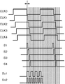
パルス選択回路105は、パルス検出器33から出力される周波数制御信号に基づいて信号S1ないし信号Snの各波形を組み合わせて、所望の波形(または周波数)の局発信号Soを生成する。図5には、上から下へ順に、クロック信号CLK0ないしクロック信号CLK4、信号S1ないし信号S4、および、局発信号So1、So2が示されている。なお、図5に示すクロックCLK0は、遅延線回路106を介した信号である。局発信号So1、So2は、図4に示す発振器31aによって生成される局発信号Soの一生成例である。また、クロック信号CLK0ないしクロック信号CLKnの間には、遅延線回路1041ないし遅延線回路104nによって遅延時間τが発生している。すなわち、各遅延線回路1041〜104nの遅延時間は、時間τであり、クロック信号CLKnは、前段のクロック信号CLKn−1に対して遅延クロック信号となり、クロック信号CLKnは、前段のクロック信号CLKn−1に対して遅延時間τだけ遅延している。図4に示す発振器31aでは、信号S1ないし信号Snは、図5に示すように、パルス幅が遅延時間τであって遅延時間τだけ順次にずれたパルスである。したがって、例えば、信号S1ないし信号Snを2個おきに2個ずつ用いることによって、パルス幅が2×τであって周期が4×τであるパルス状の局発信号So1が生成され、また例えば、信号S1ないし信号Snを1個おきに1個ずつ用いることによって、パルス幅がτであって周期が2×τであるパルス状の局発信号So2が生成される。
The
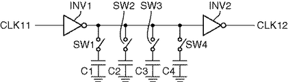
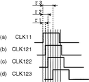
遅延線回路104(1041〜104n)は、例えば、図6に示すように、2個のインバータ素子INV1、INV2と、コンデンサCとスイッチSWとから成る1または複数の直列回路とを備えて構成され、一方のインバータ素子INV1の出力が他方のインバータ素子INV2の入力に接続され、インバータ素子INV1の出力とグランドレベルとの間には、1または複数の前記直列回路が接続される。図6に示す例では、4個の直列回路(コンデンサC1〜C4、スイッチSW1〜SW4)が接続されている。各直列回路のスイッチSW1〜SW4は、パルス検出器33から出力される周波数制御信号によってオン/オフ制御される。スイッチSW1〜スイッチSW4のオン/オフ制御によってインバータ素子INV1の出力に接続される静電容量が変化し、例えば、図7(a)〜(d)に示すように、遅延線回路104に入力されるクロック信号CLK11と遅延線回路104から出力されるクロック信号CLK12との間には、前記静電容量による遅延時間τ(図5参照)が生じる。なお、図6および図7に示す例では、各コンデンサC1〜C4の各静電容量は、0、C、2C、3C、・・・、15Cの静電容量が得られるように、C、2C、4C、8Cとなっている。例えば、図7(a)に示すクロック信号CLK11において、スイッチSW1のみがオン状態である場合に、遅延線回路104から出力されるクロック信号CLK12は、クロック信号CLK11に対して図7(b)に示す遅延時間τ1を発生したクロック信号CLK121となり、また例えば、スイッチSW2のみがオン状態である場合に、遅延線回路104から出力されるクロック信号CLK12は、クロック信号CLK11に対して図7(c)に示す遅延時間τ2(=2×τ1)を発生したクロック信号CLK122となり、また例えば、スイッチSW3のみがオン状態である場合に、遅延線回路104から出力されるクロック信号CLK12は、クロック信号CLK11に対して図7(d)に示す遅延時間τ3(=4×τ1)を発生したクロック信号CLK123となる。
The delay line circuit 104 (1041 to 104n) includes, for example, two inverter elements INV1 and INV2, and one or a plurality of series circuits including a capacitor C and a switch SW, as shown in FIG. The output of one inverter element INV1 is connected to the input of the other inverter element INV2, and one or more series circuits are connected between the output of the inverter element INV1 and the ground level. In the example shown in FIG. 6, four series circuits (capacitors C1 to C4, switches SW1 to SW4) are connected. The switches SW <b> 1 to SW <b> 4 of each series circuit are ON / OFF controlled by a frequency control signal output from the
このようにパルス検出器33から出力される周波数制御信号によって、パルス選択回路105が信号S1ないし信号Snの各波形を組み合わせるとともに、遅延線回路104の遅延時間τを制御することによって、局発信号Soの波形および周波数f2が任意に制御される。また、発振器31aは、図4に示すように比較的簡易な回路で構成され、低消費電力が可能となる。また、送信信号の周波数に応じて局発信号Soの周波数を調整することもできるので、複数の周波数の異なる送信信号に対応可能となる。
In this manner, the
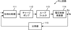
また、上述の実施形態において、発振器31aは、PLL(Phase-Looked Loop、位相同期ループ)回路を用いて構成されてもよい。図8は、図1に示す受信装置における発振器に用いることができるPLL回路の構成を示すブロック図である。PLL回路は、一般に、図8に示すように、位相比較器111、チャージポンプ112、ループフィルタ113および電圧制御発振器114の直列回路と、電圧制御発振器114の出力から位相比較器111へのフィードバック経路に設けられた分周器115とを備えて構成される。そして、発振器31aに用いる場合、電圧制御発振器114の出力が局発信号Soとされ、遅延線回路104をPLL回路の少なくとも一部で構成することによって、発振器31aに、一般的なPLL回路を用いることができ、コスト面で有利となる。なお、PLL回路以外に、DLL(Delay-Looked Loop、遅延同期ループ)回路、FLL(Frequency-Looked Loop、周波数同期ループ)回路を用いて発振器31aを構成することも可能である。
In the above-described embodiment, the
このように発振器31aから出力される局発信号Soの周波数f2が調節可能とされているので、干渉波等の中間信号がフィルタ32の通過帯域外になるように局発信号Soの周波数f2を調節することが可能となり、このような調節によって干渉波等を除去することができる可能性が高くなる。つまり、干渉波等の影響が低減され得る。また、パルス検出器33において、目的波に対応する中間信号の信号レベルが大きくなるように局発信号Soの周波数f2を調節することも可能である。さらに、発振器31aへの周波数制御信号と上述したフィルタ32への帯域制御信号とは、連動させて制御されることが望ましい。特に、干渉波等を除去するためのノッチフィルタの中心周波数は、干渉波に関する中間信号と一致させる必要があることから、周波数制御信号と帯域制御信号とは、連動させることが望ましい。
Since the frequency f2 of the local oscillation signal So output from the
ここで、上述の説明から分かるように、本実施形態のパルス抽出部3では、干渉波等を目的波から分離するために、受信期間Wrを目的波に合わせて設定する技術と、干渉波等の存在する周波数帯域を目的波から分離する技術と、干渉波等と目的波との信号レベルのレベル差によって干渉波等を分離する技術とは、併用される。つまり、パルス抽出部3において、受信信号Srから目的波を抽出する時間を制限することによって、受信装置Rxの消費電力が低減されるとともに、目的波とは異なる時刻に発生している干渉波等が除去され、かつ目的波と略同時刻に発生している干渉波等は周波数成分の相違や信号レベルのレベル差を利用することで除去される。
Here, as can be seen from the above description, in the
パルス抽出部3において、干渉波等が物理的に除去されているが、干渉波等が完全に除去されているとは限らない。このため、パルス抽出部3の出力がビット判定部4によって論理的に判断され、パルス抽出部3で抽出されたビット値が正しくない場合には、当該データが破棄される。ビット値の正否は、送信装置Txから無線信号を伝送する際にデータの前にビット同期パルス列SB(図9参照)を挿入しておき、受信装置Rx(ビット判定部4)においてビット同期パルス列SBを照合することにより、確認されればよい。なお、ビット判定部4において、いわゆるチェックサムのような符号誤りの検出技術を用いることによってもビット値の正否を確認することが可能である。データを破棄した場合には、再送要求等の周知の通信処理が行われる。
In the
以上の説明から分かるように、受信装置Rxは、送信装置Txの送信窓Wtに受信期間Wrを同期させる必要があるが、ここで、パルス検出器33において、受信期間Wrの開始タイミングを決定する機能について、より具体的に説明する。図9(a)および(b)は、UWB通信方式の無線信号におけるフレームの構成を示す図である。
As can be seen from the above description, the reception device Rx needs to synchronize the reception period Wr with the transmission window Wt of the transmission device Tx. Here, the
受信期間Wrは、例えば、送信装置Txが目的波を発生するタイミングと、受信装置Rxが発振器31aから局発信号Soを発生させるタイミングとが一致するように決定される。これら両タイミングが一致する状態は、UWB通信方式の通信信号の送受信において、送信装置Txと受信装置Rxとが同期して動作することに相当する。送信装置Txと受信装置Rxとを同期させるために、送信装置Txから送出される無線信号の1フレームは、例えば、図9(a)に示すように、同期用パルス列SYを含んでいる。また、フレームには、上述したように、ビット判定部4で用いるビット同期パルス列SBも含まれる。そして、このフレームには、これら同期用パルス列SYとビット同期パルス列SBとの後にデータパルス列DTが含まれる。一方、受信装置Rxのパルス検出器33は、図9(b)に示す同期用パルス列SYを用いて送信装置Txに同期するように、受信期間Wrのタイミングを設定する。
The reception period Wr is determined, for example, so that the timing at which the transmission device Tx generates the target wave coincides with the timing at which the reception device Rx generates the local oscillation signal So from the
この同期用パルス列SYには、図9(b)に示すように、データパルス列DTと同様に超短パルス波が用いられる。なお、データパルス列DTでは、上述したように、送信窓Wtにおける超短パルス波の列の有無によってビット値を表している。一方、同期用パルス列SYでは、すべての送信窓Wtにおいて超短パルス波の列が存在するように、一定周期で超短パルス波が発生される。 As shown in FIG. 9B, an ultrashort pulse wave is used for the synchronization pulse train SY as in the data pulse train DT. In the data pulse train DT, as described above, the bit value is represented by the presence or absence of a train of ultrashort pulse waves in the transmission window Wt. On the other hand, in the synchronization pulse train SY, an ultrashort pulse wave is generated at a constant period so that a train of ultrashort pulse waves exists in all the transmission windows Wt.
同期用パルス列SYが発生している期間では、パルス検出器33は、受信期間Wrの開始タイミングを探索するサーチモードで動作する。このサーチモードでは、受信期間Wrを設ける時間間隔が変化され、同期用パルス列SYの受信タイミングが検出される。この時間間隔は、送信窓Wtが生成される時間間隔よりも短く設定される。例えば、受信期間Wrを設ける時間間隔が毎回変化されており、同期用パルス列SYの個数と受信期間Wrの時間間隔とを適宜に設定しておくことによって、同期用受信パルス列SYが受信されている間のいずれかの受信期間Wrにおいて、同期用パルス列SYに含まれる超短パルス波の周波数変換がなされ、フィルタ32から当該超短パルス波に対応する中間信号Sbが得られる。パルス検出器33は、このフィルタ32から出力される中間信号Sb(図2(e)参照)の積分値を所定の閾値と比較し、信号レベルが前記所定の閾値に達していない中間信号は、干渉波等として除外する。
During the period in which the synchronization pulse train SY is generated, the
なお、送信装置Txの他に無線信号を送信するシステム(装置)が存在する場合に、パルス検出器33は、積分値が前記所定の閾値に達しない中間信号から当該システムによって発生する干渉波等を検出して干渉波検出信号を出力する干渉波検出部をさらに備えてもよく、これによって目的とする超短パルス波と干渉波等との識別が可能となる。
When there is a system (apparatus) that transmits a radio signal in addition to the transmission apparatus Tx, the
同期用パルス列SYが発生している期間内のいずれかの受信期間Wrにおいて、同期用パルス列SYに含まれる超短パルス波が検出されると、パルス検出器33は、サーチモードから、データを取得するためのデータモードに移行し、当該受信期間Wrの後の受信期間Wrの時間間隔を、送信装置Txにおいて送信窓Wtが生成される時間間隔と略一致する時間間隔に切り換える。この動作によって、送信装置Txと受信装置Rxとを同期させることができる。データモードでは、パルス検出器33は、受信期間Wrごとの積分値を閾値と比較し、積分値と閾値との大小関係をパルス検出信号Scとして出力する。例えば、積分値が閾値以上である場合にはビット値の1に対応する信号から成るパルス検出信号Scが出力され、積分値が前記閾値より小さい場合にはビット値の0に対応する信号から成るパルス検出信号Scが出力される。
When an ultrashort pulse wave included in the synchronization pulse train SY is detected in any reception period Wr within the period in which the synchronization pulse train SY is generated, the
このようにパルス検出器33は、サーチモードによって受信期間Wrに一致するパルスの位置識別を行い、すなわち、送信装置Txが送信窓Wtを生成した時刻を識別し、データモードにおいて当該位置におけるパルスの有無を識別する。なお、前記位置は、時間軸上の位置(時間的な位置)である。
In this way, the
以上のように、パルス検出器33は、通常では、受信期間Wrの時間間隔を変化させるサーチモードで動作し、サーチモードにおけるいずれかの受信期間Wrで超短パルス波を検出すると、送信装置Txから送出される無線信号の1フレームが終了するまでは、受信期間Wrを送信窓Wtが生成される時間間隔に一致させるデータモードで動作する。無線信号の1フレームの終了は、例えば、フレームの終了を示すシーケンスが検出され、ビット判定部4からフレームの終了が通知されることによって判断される。また例えば、この終了は、パルス検出信号Scを生成しない状態が所定の規定時間に達することによって判断される。サーチモードとデータモードとは、その受信期間Wrが異なるから、タイミング制御信号を伸長器31に与えることによって、発振器31aにおける駆動期間(発振期間、受信期間Wr)のタイミングおよび前記駆動期間の時間幅のうちの少なくとも一方が制御される。
As described above, the
そして、ビット判定部4は、サーチモードで超短パルス波を検出するまでは動作を停止しており、超短パルス波が検出された後から無線信号の1フレームが終了するまで判定動作をした後に、再びその動作を停止する。このようにビット判定部4は、必要な場合にのみ動作するので、受信装置Rxの消費電力を低減することができる。
The
なお、送信装置Txおよび受信装置Rxは、少なくとも時間間隔を計時する図略の計時手段を備えており、両者の計時手段は、1フレームの伝送に要する時間内では誤差が無視できる精度を有している。また、ノンコヒーレント方式のUWB通信方式では、パルス検出器33において、目的波の抽出ができればよく、フィルタ32を通過した中間信号Sbの全部を用いる必要がないことから、中間信号Sbの周波数には、高い安定性は要求されない。したがって、発振器31aから出力される局発信号Soの周波数f2についても高い安定性は、要求されず、このことからも設計が容易になる。
Note that the transmitting device Tx and the receiving device Rx are provided with at least time measuring means (not shown) for measuring the time interval, and both time measuring means have such accuracy that an error can be ignored within the time required for transmission of one frame. ing. Further, in the non-coherent UWB communication method, the
次に、別の実施形態について説明する。 Next, another embodiment will be described.
(第2実施形態)
図10は、第2実施形態における受信装置の物体検出動作を説明するための図である。図11は、第2実施形態における受信装置のマルチパスを考慮した物体検出動作を説明するための図である。図11(A)は、マルチパスによる物体の検出を説明するための図であり、図11(B)は、受信装置Rxの走査方法を説明するための図である。(Second Embodiment)
FIG. 10 is a diagram for explaining the object detection operation of the receiving apparatus according to the second embodiment. FIG. 11 is a diagram for explaining an object detection operation in consideration of multipath of the receiving device according to the second embodiment. FIG. 11A is a diagram for explaining object detection by multipath, and FIG. 11B is a diagram for explaining a scanning method of the receiving device Rx.
第2実施形態における受信装置Rxは、UWB方式の送信信号が、ノンコヒーレントでデータを伝送するための通信信号に代えて、一定の時間間隔で配列された短パルス波であって、前記送信信号を送信する送信装置Txから送信された無線信号(短パルス波)が物体に当たって反射した反射波を受信することによって、送信波と受信波との時間差に基づく前記物体までの距離、および受信波の時間的な強度変動に基づく前記物体の運動を検出する装置である。このような第2実施形態の受信装置Rxは、第1実施形態における受信装置Rxと略同様なハードウェア構成を備えており、その動作が次の点で異なるものである。 The receiving device Rx according to the second embodiment is configured such that a UWB transmission signal is a short pulse wave arranged at regular intervals instead of a non-coherent communication signal for transmitting data. By receiving the reflected wave reflected by the radio signal (short pulse wave) transmitted from the transmitting device Tx transmitting the signal, the distance to the object based on the time difference between the transmitted wave and the received wave, and the received wave It is a device for detecting the motion of the object based on temporal intensity fluctuations. The receiving device Rx according to the second embodiment has a hardware configuration substantially similar to that of the receiving device Rx according to the first embodiment, and the operation differs in the following points.
すなわち、第2実施形態の受信装置Rxは、送信装置Txが前記一定の時間間隔(短パルス波送信間隔)で短パルス波を送信している場合に、図10に示すように、受信期間Wr(積分器33aの積分開始時刻)を所定の時間間隔で順次にずらすことによって受信期間Wrを走査し、この走査によって得られた各受信期間Wrにおける積分器33aの各積分値と所定の閾値(物体検出閾値)とを比較し、この比較の結果、前記所定の閾値(物体検出閾値)以上である積分器33aの積分値を与える受信期間Wrに対応する短パルス波の発射時刻からの経過時間に基づいて物体までの距離を算出するものである。例えば、図10に示すように、短パルス波の発射時刻を時刻0とした場合に、時刻t2の受信期間Wrにおける積分器33aの積分値が前記所定の閾値以上となった場合では、光速をCとすれば、物体までの距離Lは、L=C・t/2によって算出することができる。
That is, the receiving device Rx according to the second embodiment has a receiving period Wr as shown in FIG. 10 when the transmitting device Tx transmits a short pulse wave at the predetermined time interval (short pulse wave transmission interval). The reception period Wr is scanned by sequentially shifting (the integration start time of the
また、第2実施形態の受信装置Rxは、パルス検出器33によって或る1つの受信期間Wrにおいて積分器33aの積分値を複数回測定し、これら各測定による各積分値の分散値に基づいて前記物体の運動の有無を検出することも可能である。すなわち、第2実施形態の受信装置Rxは、前記中間信号から、目的とするパルスの識別および到来時刻識別を行ってパルス検出信号を出力するパルス検出器33と、パルス検出器33から出力されるパルス検出信号に基づいて前記物体の運動の有無を検出する図略の物体運動検出部とをさらに備え、パルス検出器33は、目的とするパルスを識別した到来時刻において、物体からの反射波を複数回受信してその受信強度を前記パルス検出信号として出力し、前記物体運動検出部は、この反射波を複数回受信することによって得られた各受信強度の分散値に基づいて前記物体の運動の有無を検出するものである。このように構成することによって、より精度よく物体の運動の有無を検出することができる。
In the receiving device Rx of the second embodiment, the
一般に、対象の物体が完全に静止している場合には、送信装置Txから放射された短パルス波は、前記物体および近接の静止物体へ常に略同様に当たり方をするため、受信装置Rxで受信される反射波の受信強度は、略一定であるから、或る1つの受信期間Wrにおける積分器33aの各積分値の分散値は、比較的小さくなる。本実施形態の場合、反射波の電力強度の分散を検出するが、この分散は、近接する静止物体の反射波、ならびに、運動する物体の詳細各部位の各々の反射波を同時に受信した合成波の振幅強度変動により引き起こされる。したがって、たとえ運動的にごく微動であっても運動している物体が存在する場合には、送信装置Txから放射された短パルス波は、前記運動物体の各詳細部位への当たり方が時々刻々と変化するため、前記受信合成波強度がゆらぎ、前記或る1つの受信期間Wrにおける積分器33aの各積分値の分散値は、比較的大きくなる。したがって、第2実施形態の受信装置Rxは、物体検出閾値を用いた上述の動作によってまず物体を予備的に検出し、さらに、この物体を検出した受信期間Wrにおいて積分器33aの積分値を複数回測定し、これら各測定による各積分値の分散値と所定の閾値(物体運動検出閾値)とを比較し、この比較の結果、前記分散値が前記所定の閾値(物体運動検出閾値)以上である場合に、この物体検出閾値を用いて検出された物体が運動している物体の存在を判断する手段等を取ることができる。
In general, when the target object is completely stationary, the short pulse wave radiated from the transmission device Tx always strikes the object and a nearby stationary object in substantially the same manner, and thus is received by the reception device Rx. Since the reception intensity of the reflected wave is substantially constant, the dispersion value of each integral value of the
なお、上述において、物体の検出と物体の運動の検出とを纏めて行うべく、受信装置Rxは、各受信期間Wrにおいて積分器33aの積分値を複数N回測定するように構成されてもよい。また、送信装置Txから放射される短パルス波の放射強度や物体までの距離や物体の反射特性等にも拠るが、通常、物体からの反射波の強度は、小さい。このため、積分器33aにおける1つの積分値を得るために、送信装置Txが複数K回短パルス波を送信している間に、受信装置Rxは、1つの受信期間Wrにおいて積分器33aで複数K回分の積分を行って積分器33aの積分値を測定するように構成されてもよい。したがって、前記複数N回の測定とこの複数K回分の積分とを行う場合には、送信装置Txは、複数N×K回の短パルス波の送信を行うことになる。
In the above description, the receiving device Rx may be configured to measure the integral value of the
このように第2実施形態における送信装置Txと受信装置Rxとは、アクティブ方式で物体までの距離や物体の運動を検出する物体検出システムを構成している。 As described above, the transmission device Tx and the reception device Rx in the second embodiment constitute an object detection system that detects the distance to an object and the motion of the object by an active method.
また、このようなノンコヒーレントで物体を検出するシステムでは、物体からの反射波の強度に基づいて検出しているため、受信装置Rxは、直接的に反射波を受信することによって得られた積分器33aの積分値と、マルチパスで反射波を受信することによって得られた積分器33aの積分値とを区別することが困難である。すなわち、受信装置Rxは、送信装置Txから放射された短パルス波が直接物体に当たって物体により反射し、この反射波が受信装置Rxで直接受信されることによって得られる積分器33aの積分値と、送信装置Txから放射された短パルス波に起因する物体の反射波を受信装置Rxで受信されるまでの間に、1または複数の他の物体に当たって1または複数回再反射することによって得られる積分器33aの積分値とを区別することが困難である。このため、上述の物体検出動作では、図11(A)に示すように、直接的に受信されることによって得られる積分器33aの積分値に基づいて検出された物体(既検出)は、マルチパスによってゴーストとして再度検出されることになる。
In addition, in such a non-coherent system for detecting an object, detection is performed based on the intensity of a reflected wave from the object, so that the receiving device Rx directly integrates the reflected wave. It is difficult to distinguish the integration value of the
このため、第2実施形態の受信装置Rxは、図11(B)に(1)、(2)、(3)、(4)、・・・と示すように、受信装置Rxから離れる方向へ順次に、すなわち、受信装置Rxに近い領域から受信装置Rxから遠い領域へ向けて順次に物体の検出を行い、最初に物体が検出された場合において物体との距離や物体の運動を測定するように構成されてもよい。あるいは、第2実施形態の受信装置Rxは、図11(B)に、・・・、(4)、(3)、(2)、(1)と示すように、受信装置Rxから近接する方向へ順次に、すなわち、受信装置Rxに遠い領域から受信装置Rxから近い領域へ向けて順次に物体の検出を行い、最初に物体が検出された場合において物体との距離や物体の運動を測定するように構成されてもよい。このように構成することによって、受信装置Rxは、マルチパスの影響を低減し、物体との距離や物体の運動をより精度よく測定することが可能となる。特に、屋内では反射体が比較的多く存在するため、このようなマルチパスを考慮した物体検出動作は、有用である。 For this reason, the receiving device Rx of the second embodiment moves away from the receiving device Rx as indicated by (1), (2), (3), (4),... In FIG. Sequentially, that is, an object is detected sequentially from a region close to the receiving device Rx to a region far from the receiving device Rx, and when the object is first detected, the distance to the object and the motion of the object are measured. May be configured. Alternatively, the receiving device Rx of the second embodiment is in the direction of approaching from the receiving device Rx as shown in FIG. 11B as... (4), (3), (2), (1). The objects are sequentially detected from the region far from the receiving device Rx toward the region close to the receiving device Rx, and when the object is first detected, the distance to the object and the motion of the object are measured. It may be configured as follows. With this configuration, the receiving device Rx can reduce the influence of multipath and can measure the distance to the object and the movement of the object with higher accuracy. In particular, since there are a relatively large number of reflectors indoors, such an object detection operation considering multipath is useful.
このように動作することによって、第2実施形態の受信装置Rxは、送信波と受信波との時間差に基づく物体までの距離や、受信波の時間的な強度変動に基づく前記物体の運動を検出することができる。 By operating in this way, the receiving device Rx of the second embodiment detects the distance to the object based on the time difference between the transmitted wave and the received wave and the movement of the object based on the temporal intensity fluctuation of the received wave. can do.
次に、別の実施形態について説明する。 Next, another embodiment will be described.
(第3実施形態)
図12は、第3実施形態における受信装置の構成を示すブロック図である。図13は、図12に示す受信装置における各部の信号波形を説明するための図である。(Third embodiment)
FIG. 12 is a block diagram illustrating a configuration of a receiving device according to the third embodiment. FIG. 13 is a diagram for explaining signal waveforms of respective units in the receiving apparatus shown in FIG.
第3実施形態における受信装置Rxは、UWB方式の送信信号が、ノンコヒーレントでデータを伝送するための通信信号に代えて、一定の時間間隔で配列された短パルス波であって、前記送信信号を送信する送信装置Txから送信された無線信号(短パルス波)が物体に当たって反射した反射波を受信することによって、送信波と受信波との時間差に基づく前記物体までの距離、および受信波の時間的な強度変動に基づく前記物体の運動を検出する装置であり、例えば、図12に示す構成を備えている。すなわち、図12に示す第3実施形態の受信装置Rxは、図1に示す第1実施形態の受信装置Rxと較べて、パルス検出器33が積分部33aの他にさらに積分部33cを備えている点で、相違している。なお、第1実施形態と同様の構成には同一の符号を付し、その説明を省略する。第3実施形態の受信装置Rxは、送信装置Txと一体に構成されてもよい。
In the receiving device Rx according to the third embodiment, a UWB transmission signal is a short pulse wave arranged at a constant time interval instead of a communication signal for transmitting data non-coherently, and the transmission signal By receiving the reflected wave reflected by the radio signal (short pulse wave) transmitted from the transmitting device Tx transmitting the signal, the distance to the object based on the time difference between the transmitted wave and the received wave, and the received wave This is a device for detecting the motion of the object based on temporal intensity fluctuations, and has, for example, the configuration shown in FIG. That is, in the receiving device Rx of the third embodiment shown in FIG. 12, the
第3実施形態のパルス検出器33は、2つの積分部33a、33cを備えている。これら積分部33a、33cは、互いに異なるタイミングで例えば図13(d)および(e)に示す積分期間Wg1、Wg2がそれぞれ設定されており、フィルタ32が出力する中間信号Sbを積分期間Wg1、Wg2においてそれぞれ積分する。そして、2つの積分期間Wg1、Wg2でそれぞれ積分された各積分値のうちの少なくとも一方が閾値以上となる範囲において、これら2つの積分値が等しくなるように積分部33a、33cの各積分期間Wg1、Wg2のタイミングを変化させ(図13(e)の矢印参照)、2つの積分期間Wg1、Wg2の合成期間の中心を受信期間Wrの中心とすることによって、受信期間Wrと図13(c)に示す受信パルスP(目的とする超短パルス波)との同期が取られている。なお、図13(a)は、送信装置Txから送信された無線信号を受信することによって得られた受信信号Srの波形であり、図13(b)は、発振器31aが出力する局発信号Soである。局発信号Soは、受信期間Wrにおいてのみ出力されている。
The
このように2つの積分部33a、33cを用いることによって受信期間Wrと受信パルスPとの同期が取られるので、移動している物体との距離や、前記物体の移動を精度よく検出することが可能となる。また、送信装置Txの基準周波数と受信装置Rxの基準周波数との間に誤差が生じた場合でも、受信期間Wrと受信パルスPとの同期を取ることができる。なお、一般に、基準周波数の生成に用いられる水晶振動子の周波数偏差は、±10ppm(=10×10−6)程度であり、例えば、基準周波数が20MHzである場合には周波数偏差は、20±0.0002MHz程度となる。As described above, since the reception period Wr and the reception pulse P are synchronized by using the two
また、このように2つの積分部33a、33cを用いることによって、積分期間Wg1の積分器33aの積分値と、積分期間Wg2の積分器33cの積分値との大小を比較することによって、物体との距離の遠近や、前記物体の移動方向を検出することもでき、より精度よく、物体との距離や、前記物体の移動を検出することが可能となる。例えば、短パルス波の送信間隔と受信期間Wrとが一定の場合であって積分器33aの積分開始よりも後に積分器33cの積分開始が行われる場合において、或る時刻における積分期間Wg1の積分器33aの積分値が積分期間Wg2の積分器33cの積分値より大きい場合では、積分期間Wg2の受信期間Wrに基づいて算出される物体との距離よりも実際の物体の距離は、受信装置Rxに近く存在していると判断することができ、一方、逆に、或る時刻における積分期間Wg1の積分器33aの積分値が積分期間Wg2の積分器33cの積分値より小さい場合では、積分期間Wg1の受信期間Wrに基づいて算出される物体との距離よりも実際の物体の距離は、受信装置Rxから離れて存在していると判断することができる。また、前記大小の比較を経時的に行うことによって前記物体の移動方向を検出することが可能となる。例えば、短パルス波の送信間隔と受信期間Wrとが一定の場合であって積分器33aの積分開始よりも後に積分器33cの積分開始が行われる場合において、或る時刻における積分期間Wg1の積分器33aの積分値が積分期間Wg2の積分器33cの積分値より大きく、前記或る時刻から所定時間経過後の他の時刻における積分期間Wg1の積分器33aの積分値が積分期間Wg2の積分器33cの積分値より小さくなった場合では、検出されている物体は、受信装置Rxから離れる方向に移動していると判断することができる。一方、前記場合と逆の場合では、検出されている物体は、受信装置Rxに近づく方向に移動していると判断することができる。このように受信装置Rxは、2つの積分部33a、33cを備え、或る1つの受信期間Wrに対し各積分部33a、33cの積分開始タイミングを互いにずらすことによって、物体との遠近や移動する物体の移動方向を検出することが可能となる。
In addition, by using the two
なお、上述の第3実施形態において、受信装置Rxは、パルス検出器33を複数備え、各パルス検出器33における各積分部33aの積分開始タイミングが予め設定された所定時間だけ互いにずれて設定されるように構成されてもよい。この構成によれば、各積分部33aの各積分値の大小を比較し、最も大きな積分値を与える積分部33を探索することができ、この最も大きな積分値を与える積分部33における積分開始タイミングを用いることで受信信号のピーク時刻をより精度よく検出することができ、より精度よく前記物体までの距離等を検出することが可能となる。
In the third embodiment described above, the receiving device Rx includes a plurality of
また、上述の第2および第3実施形態において、受信装置Rxは、送信装置Txと一体に構成されてもよい。すなわち、受信装置Rxは、送信信号を送信する送信部をさらに備え、伸長器31の発振器31aは、ミキサ31bへ局発信号Soを出力するとともに、前記送信信号に応じた周波数の信号を前記送信部へ出力するように構成される。このように構成することによって、送信時および受信時において発振器31aが共用され、小型化およびコスト削減が可能となる。特に、前記送信部による送信信号の周波数と局発信号Soの周波数とが異なる場合であっても、上述した周波数可変な発振器31aを用いることが可能であり、このような発振器31aの性能を充分に活用することが可能となる。
In the second and third embodiments described above, the reception device Rx may be configured integrally with the transmission device Tx. That is, the receiving device Rx further includes a transmission unit that transmits a transmission signal. The
また、上述の第2および第3実施形態において、このような物体までの距離等を検出する受信装置Rxは、アンテナ1が所定の距離だけ互いに離間した複数のアンテナであって、前記複数のアンテナ1の出力を切り換えて順次に増幅部2へ入力させるスイッチ部をさらに備えて構成されてもよい。あるいは、このような物体までの距離等を検出する受信装置Rxは、アンテナ1が所定の距離だけ互いに離間した複数のアンテナであって、増幅部2が前記複数のアンテナ1にそれぞれ対応するように設けられ、前記複数の増幅部2の出力を切り換えて順次にパルス抽出部3へ入力させるスイッチ部をさらに備えて構成されてもよい。あるいは、このような物体までの距離等を検出する受信装置Rxは、アンテナ1が所定の距離だけ互いに離間した複数のアンテナであって、増幅部2およびパルス抽出部3が前記複数のアンテナ1にそれぞれ対応するように設けられて構成されてもよい。このように受信装置Rxは、複数のアンテナ1にそれぞれ対応する複数の受信系統を備えて構成されてもよい。このように構成することによって、受信装置Rxは、各アンテナ1間の距離および各アンテナ1から前記物体までの距離に基づいて、三角測量の原理によって、受信装置Rxから見た前記物体の方位を検出することが可能となる。
In the second and third embodiments described above, the receiving device Rx that detects the distance to the object is a plurality of antennas in which the
また、上述の第2および第3実施形態において、受信装置Rxは、所定の距離だけ互いに離間している複数のアンテナを備え、増幅部2は、これら複数のアンテナのいずれかから短パルス波の送信信号が放射された後に所定の時間だけ動作を停止するように構成されてもよい。あるいは、受信装置Rxは、所定の距離だけ互いに離間している複数のアンテナを備えるとともに、伸長器31のミキサ31bに後段に、伸長器31のミキサ31bの出力を増幅する増幅部2aを備え、増幅部2aは、これら複数のアンテナのいずれかから短パルス波の送信信号が放射された後に所定の時間(例えば100ps)だけ動作を停止するように構成されてもよい。図12には第3実施形態の受信装置Rxの場合について破線で増幅部2aが示されている。このように、受信装置Rxは、所定の距離だけ互いに離間している複数のアンテナを備えるとともに、伸長器31のミキサ31bの前(前段)または後(後段)に接続される増幅部2または2aを備え、この増幅器2、2aは、複数のアンテナのいずれかから短パルス波の送信信号が放射された後に所定の時間(例えば100ps)だけ動作を停止するように構成されてもよい。このように構成することによって、短パルス波の送信信号を送信するアンテナを除く残余のアンテナが、前記物体からの反射波ではなく、短パルス波の送信信号を送信するアンテナから直接的に短パルス波(直接受信波)を受信したとしても、ミキサ31bの前(前段)または後(後段)に接続される増幅部2、2aが短パルス波の送信信号の放射後、所定の時間だけ、その動作を停止するので、前記直接受信波による増幅部2、2aの飽和を回避することができ、受信装置Rxは、この受信装置Rxにより近い位置に存在する物体も検知可能となる。
In the second and third embodiments described above, the receiving device Rx includes a plurality of antennas separated from each other by a predetermined distance, and the amplifying
また、上述の第2および第3実施形態において、受信装置Rxは、入力を半波整流または全波整流する整流部34をさらに備えて構成されてもよい。図12には第3実施形態の受信装置Rxの場合について破線で整流部34が示されている。このように構成することによって、パルス検出器33bの積分部33a、33cに入力される信号の極性が1つとなるので、積分部33a、33cにおける積分が容易となり、積分部33a、33cの回路構成の簡易化が可能となる。
In the second and third embodiments described above, the receiving device Rx may further include a rectifying
次に、別の実施形態について説明する。 Next, another embodiment will be described.
(第4実施形態)
第1実施形態では、送信装置Txから送信されたデータパルス列DTの受信を受信装置Rxが失敗した場合に、受信装置Rxが送信装置Txに再送要求を行う例を示したが、第4実施形態は、送信装置Txがデータパルス列DTと同じビット値を予め複数回ずつ繰り返して送信する例である。(Fourth embodiment)
In the first embodiment, the example in which the receiving device Rx makes a retransmission request to the transmitting device Tx when the receiving device Rx fails to receive the data pulse train DT transmitted from the transmitting device Tx has been described. Is an example in which the transmission device Tx repeatedly transmits the same bit value as the data pulse train DT a plurality of times in advance.
この場合、受信装置Rxは、送信装置Txが同じビット値を表す超短パルス波の送信回数分の期間を受信期間Wrに設定し、パルス検出器33の積分部33aは、受信期間Wrに同期した積分器間においてフィルタ32が出力する中間信号Sbを積分する。そして、レベル判定部33bは、積分結果に基づいて2値のレベル判定を行った結果をパルス検出信号Scとして出力する。
In this case, the reception device Rx sets a period corresponding to the number of times of transmission of the ultrashort pulse wave in which the transmission device Tx indicates the same bit value as the reception period Wr, and the
より具体的には、パルス検出器33は、データモードにおいて、積分部33aでの積分回数を比較的多く(例えば10回程度)取るとともに、レベル判定部33bにおいて積分部33aの出力を適宜な閾値で2値化することによって、目的波に干渉波等が重複(重畳)しても重複した回数が少なければ干渉波の影響を除去して目的波を抽出することが可能になり、受信感度の向上を図ることができる。積分部33aは、サーチモードにおいて積分を行わない。なお、他の構成およびその動作は、第1実施形態と同様である。また、第4実施形態は、上述の第2および第3実施形態にも適用可能であり、同様の効果を奏する。
More specifically, the
次に、別の実施形態について説明する。 Next, another embodiment will be described.
(第5実施形態)
図14は、第5実施形態における受信装置の構成を示すブロック図である。(Fifth embodiment)
FIG. 14 is a block diagram illustrating a configuration of a receiving device according to the fifth embodiment.
UWB通信方式の通信信号を受信する受信装置は、上述したように、前記通信信号のパルス信号と同期して所定の期間、例えば10nsecのウィンドウ期間においてのみ前記通信信号のパルス信号を受信することによって、UWB通信方式の通信信号のパルス信号のように一定の周期を有さない背景ノイズを排除して、有意なUWB通信方式の通信信号のパルス信号を受信している。 As described above, the receiving device that receives the communication signal of the UWB communication method receives the pulse signal of the communication signal only in a predetermined period, for example, a 10 nsec window period in synchronization with the pulse signal of the communication signal. The background signal that does not have a certain period, such as the pulse signal of the communication signal of the UWB communication system, is eliminated, and the pulse signal of the communication signal of the significant UWB communication system is received.
一方、UWB通信方式は、その一態様において、搬送波を用いず、例えばパルス幅が1nsec以下等の極めて短いパルス信号を用いるために、他の無線通信方式と比較して送信電力のスペクトル密度が非常に低い。このため、受信装置の各部を構成する各内部回路は、比較的高感度に構成されており、受信装置は、これら内部回路によって生じたノイズを信号として拾ってしまう場合がある。特に、これら内部回路において用いられているクロック信号に起因するノイズは、周期性を有するため、このような周期性を有するノイズがウィンドウ期間と同期すると、ノイズを受信パルスと誤認する場合があるため、通信の信頼性が低下してしまう。 On the other hand, the UWB communication system uses a very short pulse signal having a pulse width of 1 nsec or less, for example, without using a carrier wave in one aspect thereof, so that the spectral density of transmission power is extremely low compared to other wireless communication systems. Very low. For this reason, each internal circuit which comprises each part of a receiver is comprised by comparatively high sensitivity, and the receiver may pick up the noise produced by these internal circuits as a signal. In particular, noise caused by the clock signals used in these internal circuits has periodicity, and therefore, when such periodic noise synchronizes with the window period, the noise may be mistaken as a received pulse. The reliability of communication will be reduced.
この第5実施形態における受信装置Rxは、通信の信頼性をより向上させることができる装置であり、例えば、図14に示す構成を備えている。すなわち、図14に示す第5実施形態の受信装置Rxは、図1に示す第1実施形態の受信装置Rxと較べて、パルス検出器33が、通信の信頼性の向上を目的として、さらに、信号処理部33d、基準クロック生成部33eおよび位相制御部33fを備えている点で、相違している。なお、第1実施形態と同様の構成には同一の符号を付し、その説明を省略する。
The receiving device Rx in the fifth embodiment is a device that can further improve the reliability of communication, and has, for example, the configuration shown in FIG. That is, in the receiving device Rx of the fifth embodiment shown in FIG. 14, compared with the receiving device Rx of the first embodiment shown in FIG. 1, the
第5実施形態のパルス検出器33は、積分部33a、レベル判定部33b、信号処理部33d、基準クロック生成部33eおよび位相制御部33fを備えている。
The
信号処理部33dは、積分部33aに接続され、例えば、所定の演算処理を実行するCPU(Central Processing Unit)と、所定の制御プログラムが記憶されたROM(Read Only Memory)と、データを一時的に記憶するRAM(Random Access Memory)と、これら周辺回路等とを備えて構成される。信号処理部33dは、ROMに記憶された制御プログラムを実行することによって、機能的に、パルス信号の周期を複数の区間に分割した各区間毎に、積分部33aの出力であってディジタル信号である信号レベル値ADを取得すると共にアンテナ1によって無線によるUWB通信方式の通信信号RFが受信されていない状態において取得した区間毎の信号レベルを区間レベル記憶部33dbに区間毎に記憶させる区間レベル取得部33daと、アンテナ1により通信信号が受信されていない状態において、区間レベル取得部33daによって取得された区間ごとの信号レベルを区間ごとに記憶する区間レベル記憶部33dbと、アンテナ1により受信された区間毎の信号レベルを、区間レベル記憶部33dbに記憶されている区間毎の信号レベルに基づいて、それぞれ補正する補正部33dcとを備えて構成される。
The
基準クロック生成部33eは、例えば、水晶発振器を用いて構成されており、UWB通信方式の通信信号におけるパルス信号の周期と同じ周期のクロック信号を生成し、位相制御部33fへ出力する。
The reference
位相制御部33fは、信号制御部33dおよび基準クロック生成部33eに接続され、基準クロック生成部33eから出力されたクロック信号に基づき、動作タイミングを制御するゲート信号GTを積分部33aへ出力する。より具体的には、位相制御部33fは、UWB通信方式の通信信号におけるパルス信号のパルス幅と同程度もしくは若干パルス幅が大きい、例えば10nsecにされたパルス信号を、ウィンドウ期間を示す信号として、UWB通信方式の通信信号におけるパルス信号の周期、例えば50nsec周期でゲート信号GTとして積分部33aへ出力する。また、位相制御部33fは、信号処理部33dからの制御信号に応じてゲート信号GTにおけるウィンドウ期間を示すパルス信号のタイミングを変化させるようになっている。
The phase control unit 33f is connected to the
積分部33aは、ゲート信号GTにおけるパルス信号のタイミングと同期して信号の積分を実行し、他のタイミングでは前記積分を行わない。これにより、パルス復調部3によって、ゲート信号GTにおけるパルス信号のタイミング、すなわちウィンドウ期間においてアンテナ1で受信された通信信号RFが検波され、積分部33aで積分され、さらにその積分値が信号処理部33dへ出力されるようになっている。
The
ビット判定部4は、第1実施形態と同様に、パルス抽出部3に接続され、パルス抽出部3のパルス検出器33から出力されるパルス検出信号Scに基づいて送信装置Txから送信された無線信号のビット値を抽出する回路である。ここで、第5実施形態のビット判定部4では、補正部33dcによって補正された各区間毎の信号レベルに応じて通信信号RFの復調が行われる。
Similarly to the first embodiment, the
次に、上述のように構成された無線受信装置1の動作について説明する。図15は、図14に示す受信装置の動作を説明するための、各部の信号波形を示す図である。図15(a)は、ノイズの影響を受けない理想的な環境下における信号波形の一例を示し、図15(b)は、周期的な回路ノイズが受信信号に重畳された場合の信号波形の一例を示している。図15(a)および図15(b)には、検波信号S1、ゲート信号GTおよび積分部33aの出力信号の各信号波形が上から順に示されている。図16は、図14に示す受信装置の区間レベル取得部の動作を説明するための、各部の信号波形を示す図である。図16では、検波信号S1およびゲート信号GTの各信号波形が上から順に示されている。
図17は、図14に示す受信装置の補正部により得られる補正信号の一例を示す図である。図17の横軸は、時間であり、その縦軸は、レベルである。Next, the operation of the
FIG. 17 is a diagram illustrating an example of a correction signal obtained by the correction unit of the reception apparatus illustrated in FIG. The horizontal axis in FIG. 17 is time, and the vertical axis is level.
図15(a)に示すように、ノイズの影響を受けない理想的な環境下では、パルス抽出部3において、アンテナ1で受信された無線の通信信号RFがパルスに復調され、積分部33aに、検波信号S1として復調パルスP1が入力される。そして、位相制御部33fから出力されたゲート信号GTにおけるパルス信号のタイミング、すなわちウィンドウ期間T1において、積分部33aによって復調パルスP1が積分される。
As shown in FIG. 15 (a), under an ideal environment not affected by noise, the
一方、図15(b)に示すように、周期的な回路ノイズが受信信号に重畳された場合には、前記検波信号S1には、復調パルスP1以外にノイズが周期的に重畳され、ノイズの平均値レベルが上昇する。この場合、復調パルスP1の波高値は、ノイズの平均値レベルから復調パルスP1のピークまでの値となるので、ノイズの平均値レベルが上昇することにより復調パルスP1の波高値が減少する。このため、復調パルスP1のエネルギーが減少する結果、復調パルスP1が積分部33aにより積分されて得られる積分値が、低下し、信号レベル値ADも低下する。
On the other hand, as shown in FIG. 15B, when periodic circuit noise is superimposed on the received signal, noise is periodically superimposed on the detection signal S1 in addition to the demodulated pulse P1. The average level increases. In this case, since the peak value of the demodulated pulse P1 is a value from the average value level of the noise to the peak of the demodulated pulse P1, the peak value of the demodulated pulse P1 decreases as the average value level of the noise increases. For this reason, as a result of the energy of the demodulated pulse P1 decreasing, the integrated value obtained by integrating the demodulated pulse P1 by the integrating
また、図15(b)に示すように、復調パルスP1の波高値とノイズの波高値との差が小さくなるので、ゲート信号GTにおけるウィンドウ期間T1がノイズと同期してノイズを受信パルスと誤認するおそれがある。 Further, as shown in FIG. 15B, since the difference between the peak value of the demodulated pulse P1 and the peak value of the noise becomes small, the window period T1 in the gate signal GT is synchronized with the noise and the noise is mistakenly recognized as a received pulse. There is a risk.
そこで、受信装置Rxでは、まず、送信装置Txから無線の通信信号RFが送信されておらず、従ってアンテナ1により前記通信信号RFが受信されていない状態における信号レベル値AD、すなわち内部回路における周期ノイズに起因する各ウィンドウ期間毎の信号レベル値ADが区間レベル取得部33daによって取得される。
Therefore, in the receiving device Rx, first, the signal level value AD in a state where the wireless communication signal RF is not transmitted from the transmitting device Tx and thus the communication signal RF is not received by the
まず、アンテナ1により無線の通信信号RFが受信されていない状態では、検波信号S1には、復調パルスP1は含まれておらず、したがって、ノイズに起因する検波信号S1が積分部33aに入力される。
First, in a state where the wireless communication signal RF is not received by the
そして、まず、区間レベル取得部33daからの制御信号に応じて、位相制御部33fからウィンドウ期間T1の位相でゲート信号GTが積分部33aとへ出力され、積分部33aによって、ウィンドウ期間T1のタイミングで検波信号S1が積分され、その積分値に応じた信号レベル値ADが、区間レベル取得部33daに入力される。区間レベル取得部33daは、予め設定された所定時間、例えば8μsecの間、位相制御部33fからウィンドウ期間T1の位相でゲート信号GTを出力させる。そして、区間レベル取得部daは、8μsecの間に得られたウィンドウ期間T1における信号レベル値ADを平均し、その平均値をウィンドウ期間T1における平均レベル値AVT1として区間レベル記憶部33dbに記憶させる。
First, in response to the control signal from the section level acquisition unit 33da, the phase control unit 33f outputs the gate signal GT to the
次に、区間レベル取得部33daは、位相制御部33fからウィンドウ期間T1とは、位相のずれたタイミング、例えばウィンドウ期間T1より1nsec遅れたウィンドウ期間T2の位相でゲート信号GTを所定時間、例えば8μsecの間出力させる。そして、区間レベル取得部33daによって、8μsecの間複数周期に亘って得られたウィンドウ期間T2における信号レベル値ADが平均され、その平均値がウィンドウ期間T2における平均レベル値AVT2として区間レベル記憶部33dbに記憶される。 Next, the section level acquisition unit 33da outputs the gate signal GT from the phase control unit 33f for a predetermined time, for example, 8 μsec, at a phase shifted from the window period T1, for example, a phase of the window period T2 that is delayed by 1 nsec from the window period T1. For the duration. Then, the section level acquisition unit 33da averages the signal level value AD in the window period T2 obtained over a plurality of periods for 8 μsec, and the average value is used as the average level value AVT2 in the window period T2 as the section level storage unit 33db. Is remembered.
同様にして、区間レベル取得部33daによって、ウィンドウ期間が1nsecずつ逐次ずらされて、復調パルスP1の周期である50nsec内に設けられた50個の各ウィンドウ期間毎に得られた平均レベル値AVT1〜AVT50、すなわち内部回路における周期ノイズに起因する各ウィンドウ期間毎の信号レベル値が、区間レベル記憶部33dbに記憶される。この場合、ウィンドウ期間T1〜T50が、請求項における複数の区間の一例に相当している。 Similarly, the window level is sequentially shifted by 1 nsec by the section level acquisition unit 33da, and the average level values AVT1 to AVT1 obtained for each of the 50 window periods provided within 50 nsec that is the period of the demodulation pulse P1. AVT 50, that is, a signal level value for each window period caused by periodic noise in the internal circuit is stored in the section level storage unit 33db. In this case, the window periods T1 to T50 correspond to an example of a plurality of sections in the claims.
なお、区間レベル取得部33daは、区間レベル記憶部33dbのアドレスに各ウィンドウ期間(区間)を対応させて、各ウィンドウ期間毎の平均レベル値AVT1〜AVT50を記憶させてもよく、各ウィンドウ期間を示す識別データと平均レベル値AVT1〜AVT50とを対応させて区間レベル記憶部33dbに記憶させてもよい。 The section level acquisition unit 33da may store the average level values AVT1 to AVT50 for each window period by associating each window period (section) with the address of the section level storage unit 33db. The indicated identification data and the average level values AVT1 to AVT50 may be associated with each other and stored in the section level storage unit 33db.
次に、アンテナ1によって受信された無線の通信信号RFが、パルス抽出部3において、同様に、復調および積分され、信号レベル値ADとして補正部33dcに入力される。そして、補正部33dcによって、各ウィンドウ期間T1〜T50における信号レベル値ADから区間レベル記憶部33dbに記憶されている平均レベル値AVT1〜AVT50、すなわち内部回路における周期ノイズに起因する各ウィンドウ期間毎の信号レベル値がそれぞれ減算されることにより補正され、その補正後の補正信号S2がビット判定部(復調部)4で復調されて送信信号情報(データ)RDとして外部へ出力される。
Next, the wireless communication signal RF received by the
これにより、信号レベル値ADに、内部回路で生じた周期性を有するノイズが重畳されている場合であっても、補正部33dcによって、区間レベル記憶部33dbに記憶された平均レベル値AVT1〜AVT50、すなわち内部回路における周期ノイズに起因する各ウィンドウ期間毎の信号レベル値が、信号レベル値ADから減算されて補正され、周期性を有するノイズの影響が低減されるので、通信の信頼性を向上させることができる。 Thereby, even if the periodic noise generated in the internal circuit is superimposed on the signal level value AD, the average level values AVT1 to AVT50 stored in the section level storage unit 33db by the correction unit 33dc. In other words, the signal level value for each window period caused by periodic noise in the internal circuit is corrected by subtracting from the signal level value AD, and the influence of periodic noise is reduced, thus improving communication reliability. Can be made.
なお、区間レベル取得部33daは、平均レベル値AVT1〜AVT50を区間レベル記憶部33dbに記憶させる例に限られず、ウィンドウ期間T1〜T50における信号レベル値ADをそのまま区間レベル記憶部33dbに記憶させ、補正部33dcがウィンドウ期間T1〜T50における信号レベル値ADを用いて受信信号の補正を行ってもよいが、補正部33dcが平均レベル値AVT1〜AVT50を用いることによって、内部回路における周期ノイズに起因する各ウィンドウ期間毎における信号レベル値の測定精度が向上され、これによって通信の信頼性が向上可能となる。 The section level acquisition unit 33da is not limited to the example in which the average level values AVT1 to AVT50 are stored in the section level storage unit 33db, and the signal level value AD in the window periods T1 to T50 is stored in the section level storage unit 33db as it is. The correction unit 33dc may correct the reception signal using the signal level value AD in the window periods T1 to T50. However, the correction unit 33dc uses the average level values AVT1 to AVT50, thereby causing periodic noise in the internal circuit. The measurement accuracy of the signal level value in each window period is improved, thereby improving the reliability of communication.
また、補正部33dcは、予め設定された基準値REFと区間レベル記憶部33dbに記憶されている平均レベル値AVT1〜AVT50との差分を、各ウィンドウ期間T1〜T50における信号レベル値ADにそれぞれ加算することによって補正信号S2を生成するように構成されてもよい。より具体的には、例えば、各ウィンドウ期間T1〜T50における信号レベル値ADをAD1〜AD50として表すと、補正部33dcは、以下の式(1)に基づいて、補正信号S2を生成してもよい。
S2=ADn+(REF−AVTn) ・・・(1)
(ただし、n=1,2,3,・・・,50)Further, the correction unit 33dc adds the difference between the preset reference value REF and the average level values AVT1 to AVT50 stored in the section level storage unit 33db to the signal level value AD in each of the window periods T1 to T50. By doing so, the correction signal S2 may be generated. More specifically, for example, when the signal level value AD in each of the window periods T1 to T50 is expressed as AD1 to AD50, the correction unit 33dc generates the correction signal S2 based on the following equation (1). Good.
S2 = ADn + (REF−AVTn) (1)
(However, n = 1, 2, 3,..., 50)
この場合、基準値REFを例えば「240」とすると、図17に示すように、無線の通信信号RFが受信されていない状態における補正信号S2は、およそ基準値REFに等しく「240」となる。そうすると、例えば、復調パルスP1が負の値を取る場合であっても補正信号S2は、正の値となるので、信号処理部33dは、負の値を処理する必要がなく、信号処理が容易となる。
In this case, if the reference value REF is set to “240”, for example, as shown in FIG. 17, the correction signal S2 in a state where the wireless communication signal RF is not received becomes “240” which is approximately equal to the reference value REF. Then, for example, even if the demodulated pulse P1 takes a negative value, the correction signal S2 becomes a positive value, so that the
また、区間レベル取得部33daは、以下の式(2)で示すように、予め設定された基準値REFと平均レベル値AVT1〜AVT50との差分を、各ウィンドウ期間T1〜T50における補正値C1〜C50として区間レベル記憶部33dbに記憶させてもよい。
Cn=REF−AVTn ・・・(2)
(ただし、n=1,2,3,・・・,50)Further, the section level acquisition unit 33da uses the difference between the preset reference value REF and the average level values AVT1 to AVT50 as the correction values C1 to C1 in the window periods T1 to T50, as shown in the following equation (2). C50 may be stored in the section level storage unit 33db.
Cn = REF-AVTn (2)
(However, n = 1, 2, 3,..., 50)
そして、補正部33dcは、以下の式(3)で示すように、区間レベル記憶部33dbに記憶されている各ウィンドウ期間毎の補正値C1〜C50を、各ウィンドウ期間T1〜T50における信号レベル値AD1〜AD50にそれぞれ加算することによって補正信号S2を生成するように構成されてもよい。
S2=ADn+Cn ・・・(3)
(ただし、n=1,2,3,・・・,50)Then, as shown in the following equation (3), the correction unit 33dc uses the correction values C1 to C50 for each window period stored in the section level storage unit 33db as signal level values in the window periods T1 to T50. The correction signal S2 may be generated by adding to AD1 to AD50, respectively.
S2 = ADn + Cn (3)
(However, n = 1, 2, 3,..., 50)
これにより、補正部33dcは、無線信号RFを補正する際に、式(3)の演算処理を実行すればよいので、式(1)の演算処理を実行する場合よりも無線信号RFの受信動作時における補正部33dcの演算処理負荷が軽減可能となる。 Accordingly, the correction unit 33dc only needs to execute the calculation process of the equation (3) when correcting the radio signal RF, and therefore, the reception operation of the radio signal RF is performed more than when the calculation process of the equation (1) is executed. The calculation processing load of the correction unit 33dc at the time can be reduced.
また、無線の通信信号RFにおけるパルス周期において、50個のウィンドウ期間(区間)を設ける例を示したが、ウィンドウ期間の数(位相差)は、適宜に設定すればよい。各ウィンドウ期間の位相差を縮小してウィンドウ期間の数が増加するほど、補正精度が向上されるので、通信の信頼性が向上される。 Further, although an example in which 50 window periods (sections) are provided in the pulse period of the wireless communication signal RF has been described, the number of window periods (phase difference) may be set as appropriate. As the phase difference of each window period is reduced and the number of window periods is increased, the correction accuracy is improved, so that the reliability of communication is improved.
また、隣接するウィンドウ期間を重複させる例を示したが、隣接するウィンドウ期間が重複せず、連続するように設定されてもよい。この場合、無線信号RFのパルス周期におけるウィンドウ期間の数が減少可能となる。 Moreover, although the example which overlaps an adjacent window period was shown, the adjacent window periods may not be overlapped and you may set so that it may continue. In this case, the number of window periods in the pulse period of the radio signal RF can be reduced.
また、ウィンドウ期間を、UWB通信におけるパルス信号のパルス幅と同程度若しくは若干パルス幅が大きい10nsecに設定する例を示したが、ウィンドウ期間を増大させることによって、無線信号RFのパルス周期におけるウィンドウ期間の数が減少可能となる。この場合、ウィンドウ期間を増大させるとノイズ成分が積分される時間も増大し、S/N比(信号対ノイズ比)が低下するので、ウィンドウ期間の数を増大させることによる回路負荷の増大と、ウィンドウ期間を増大させることによるS/N比の低下とのバランスによって、適宜にウィンドウ期間が設定される。 In addition, although the example in which the window period is set to 10 nsec, which is approximately the same as or slightly larger than the pulse width of the pulse signal in UWB communication, has been shown, the window period in the pulse period of the radio signal RF is increased by increasing the window period. The number of can be reduced. In this case, when the window period is increased, the time over which the noise component is integrated also increases, and the S / N ratio (signal-to-noise ratio) decreases. Therefore, an increase in the circuit load by increasing the number of window periods, The window period is appropriately set according to the balance with the decrease in the S / N ratio by increasing the window period.
また、上述の実施形態において、受信装置Rxは、中間信号Sbの信号波全体を積分するように構成されたが、積分時間を短くすることによって、その一部分、例えば、信号波の立ち上がり部分の一部を積分するように構成されてもよい。例えば、前記積分時間は、UWB通信方式の通信信号における時間幅の約1/10(=約0.2ns)に設定される。 In the above-described embodiment, the receiving device Rx is configured to integrate the entire signal wave of the intermediate signal Sb. However, by shortening the integration time, a part thereof, for example, one of the rising parts of the signal wave. It may be configured to integrate the part. For example, the integration time is set to about 1/10 (= about 0.2 ns) of the time width in the communication signal of the UWB communication system.
本明細書は、上記のように様々な態様の技術を開示しているが、そのうち主な技術を以下に纏める。 The present specification discloses various aspects of the technology as described above, and the main technologies are summarized below.
一態様にかかる受信装置は、ウルトラワイドバンド方式の送信信号を受信する受信装置であって、前記送信信号は、ノンコヒーレントでデータを伝送するための通信信号であり、前記送信信号を受信することによって得られた受信信号の周波数変換を行って中間信号を出力する伸長器を備え、前記伸長器は、前記受信信号の中心周波数と異なる周波数で、前記受信信号に含まれる短パルスの位相および波形に依存しない波形である局発信号を出力する発振器と、前記受信信号と前記局発信号とを乗算して前記中間信号を出力するミキサとを備え、前記発振器は、前記受信信号に含まれる短パルス波の発生タイミングに同期して間欠動作するものである。 A receiving apparatus according to an aspect is a receiving apparatus that receives a transmission signal of an ultra-wide band method, wherein the transmission signal is a communication signal for transmitting data non-coherently and receives the transmission signal. And a decompressor that performs frequency conversion of the received signal obtained by the step S1 and outputs an intermediate signal, and the expander has a phase and waveform of a short pulse included in the received signal at a frequency different from the center frequency of the received signal. And a mixer that multiplies the received signal by the local signal and outputs the intermediate signal, and the oscillator includes a short signal included in the received signal. The operation is intermittent in synchronization with the generation timing of the pulse wave.
この構成によれば、発振器は、間欠動作され、常に、動作しないので、UWB通信方式を用いて、消費電力を低減することが可能となる。そして、伸長器は、受信信号の周波数変換を行うので、ダウンコンバートする場合には、間欠駆動の駆動期間においても、低消費電力化が可能となり、また、後段にフィルタを備える場合には、そのフィルタ回路の設計の容易化や小型化やコストダウンを図ることが可能となる。 According to this configuration, since the oscillator is intermittently operated and does not always operate, it is possible to reduce power consumption using the UWB communication method. Since the expander performs frequency conversion of the received signal, when down-converting, it is possible to reduce power consumption even during the intermittent drive period, and when a filter is provided in the subsequent stage, The filter circuit can be easily designed, reduced in size, and reduced in cost.
また、他の一態様では、上述の受信装置において、前記中間信号のうち、目的とする短パルス波に相当する周波数成分を通過させるフィルタをさらに備え、前記フィルタは、前記受信信号に含まれる短パルス波の発生タイミングに同期して間欠動作可能であるものである。 According to another aspect, the receiving apparatus further includes a filter that allows a frequency component corresponding to a target short pulse wave to pass among the intermediate signal, and the filter is a short signal included in the received signal. The intermittent operation is possible in synchronization with the generation timing of the pulse wave.
この構成によれば、フィルタは、間欠動作可能とされ、常に、動作しないので、UWB通信方式を用いて、消費電力を低減することが可能となる。 According to this configuration, the filter can be intermittently operated and does not always operate. Therefore, it is possible to reduce power consumption using the UWB communication method.
また、他の一態様では、これら上述の受信装置において、前記中間信号から、目的とするパルスの識別および到来時刻識別を行ってパルス検出信号を出力するパルス検出器をさらに備え、前記パルス検出器は、前記受信信号に含まれる短パルス波の発生タイミングに同期して間欠動作可能であるものである。 According to another aspect, in the above-described receiving device, the pulse detector further includes a pulse detector that performs pulse identification and arrival time identification from the intermediate signal and outputs a pulse detection signal. Is capable of intermittent operation in synchronization with the generation timing of a short pulse wave included in the received signal.
この構成によれば、パルス検出器は、間欠動作可能とされ、常に、動作しないので、UWB通信方式を用いて、消費電力を低減することが可能となる。 According to this configuration, the pulse detector can be intermittently operated and does not always operate. Therefore, the power consumption can be reduced by using the UWB communication method.
また、他の一態様では、これら上述の受信装置において、前記中間信号から、目的とするパルスの識別および到来時刻識別を行ってパルス検出信号を出力するパルス検出器をさらに備え、前記通信信号は、予め設定された所定の複数回ずつ連続して同じビット値を表す短パルス波を含み、前記パルス検出器は、前記複数回の期間において中間信号を積分する積分部と、前記積分部の積分結果に基づいて2値のレベル判定を行った結果をパルス検出信号として出力するレベル判定部とを備えるものである。 According to another aspect, the above-described receiving device further includes a pulse detector that outputs a pulse detection signal by identifying a target pulse and an arrival time from the intermediate signal, and the communication signal is A short pulse wave that represents the same bit value continuously in a plurality of predetermined times, and the pulse detector includes an integration unit that integrates an intermediate signal in the plurality of times, and integration of the integration unit A level determination unit that outputs a result of performing binary level determination based on the result as a pulse detection signal.
この構成によれば、目的波に干渉波等が重複しても、干渉波等の影響が略除去され、目的波の抽出が可能となり、受信感度の向上を図ることが可能となる。 According to this configuration, even if an interference wave or the like overlaps with the target wave, the influence of the interference wave or the like is substantially removed, the target wave can be extracted, and reception sensitivity can be improved.
また、他の一態様では、上述の受信装置において、前記積分部および前記レベル判定部のうちの少なくとも一方は、前記受信信号に含まれる短パルス波の発生タイミングに同期して間欠動作するものである。 According to another aspect, in the receiving device described above, at least one of the integrating unit and the level determining unit operates intermittently in synchronization with the generation timing of a short pulse wave included in the received signal. is there.
この構成によれば、積分部およびレベル判定部のうちの少なくとも一方は、間欠動作され、常に、動作しないので、UWB通信方式を用いて、消費電力を低減することが可能となる。 According to this configuration, since at least one of the integration unit and the level determination unit is intermittently operated and does not always operate, power consumption can be reduced using the UWB communication method.
また、他の一態様では、上述の受信装置において、前記パルス検出器が出力したパルス検出信号から前記データのビット値を取り出すビット判定部をさらに備え、前記ビット判定部は、前記パルス検出器が目的とするパルスを識別した後に動作するものである。 In another aspect, the receiving device further includes a bit determination unit that extracts a bit value of the data from the pulse detection signal output from the pulse detector, and the bit determination unit includes the pulse detector. It operates after identifying the target pulse.
この構成によれば、パルス検出器が目的とするパルスを識別する以前における消費電力を低減することが可能となる。 According to this configuration, it is possible to reduce power consumption before the pulse detector identifies a target pulse.
また、他の一態様では、これら上述の受信装置において、前記送信信号は、無線信号であって、前記パルス検出器は、中間信号から前記送信信号を送信する送信装置の他に無線を用いたシステムが発生する干渉波を検出する検出手段をさらに備えるものである。 Moreover, in another aspect, in the above-described receiving apparatuses, the transmission signal is a radio signal, and the pulse detector uses radio in addition to the transmission apparatus that transmits the transmission signal from an intermediate signal. The apparatus further includes detection means for detecting an interference wave generated by the system.
この構成によれば、目的とする短パルス波と干渉波等との識別が可能となる。 According to this configuration, it is possible to distinguish between a target short pulse wave and an interference wave.
また、他の一態様では、これら上述の受信装置において、前記送信信号は、ノンコヒーレントでデータを伝送するための通信信号に代えて、一定の時間間隔で配列された短パルス波であって、前記送信信号を送信する送信装置から送信された短パルス波が物体に当たって反射した反射波を受信するものである。 Further, in another aspect, in the above-described receiving device, the transmission signal is a short pulse wave arranged at a constant time interval instead of a communication signal for transmitting data non-coherently, The reflected wave reflected by the short pulse wave transmitted from the transmitting apparatus that transmits the transmission signal hits the object is received.
この構成によれば、受信装置がセンサとして構成され、物体との距離や、物体の運動をより精度よく検出することが可能となる。 According to this configuration, the receiving device is configured as a sensor, and the distance to the object and the motion of the object can be detected with higher accuracy.
また、他の一態様では、上述の受信装置において、前記送信信号を送信する送信部をさらに備え、前記伸長器の前記発振器は、前記ミキサへ前記局発信号を出力するとともに、前記送信信号に応じた周波数の信号を前記送信部へ出力するものである。 According to another aspect, the receiving device further includes a transmitting unit that transmits the transmission signal, and the oscillator of the expander outputs the local oscillation signal to the mixer and outputs the local signal to the transmission signal. A signal with a corresponding frequency is output to the transmitter.
この構成によれば、送信時および受信時において発振器31aが共用され、受信装置Rxの小型化およびコスト削減が可能となる。
According to this configuration, the
また、他の一態様では、上述の受信装置において、前記送信信号は、ノンコヒーレントでデータを伝送するための通信信号に代えて、一定の時間間隔で配列された短パルス波であって、前記送信信号を送信する送信装置から送信された短パルス波が物体に当たって反射した反射波を受信するものであって、前記中間信号から、目的とするパルスの識別および到来時刻識別を行ってパルス検出信号を出力するパルス検出器と、前記パルス検出器から出力されるパルス検出信号に基づいて前記物体の運動の有無を検出する物体運動検出部とをさらに備え、前記パルス検出器は、目的とするパルスを識別した到来時刻において、前記反射波を複数回受信してその受信強度を前記パルス検出信号として出力し、前記物体運動検出部は、前記反射波を複数回受信することによって得られた各受信強度の分散値に基づいて前記物体の運動の有無を検出するものである。 Further, in another aspect, in the above-described receiving device, the transmission signal is a short pulse wave arranged at a constant time interval instead of a communication signal for transmitting data non-coherently, A short pulse wave transmitted from a transmission device that transmits a transmission signal is received by a reflected wave reflected by an object, and a pulse detection signal is obtained by identifying a target pulse and identifying an arrival time from the intermediate signal. And a body motion detector for detecting the presence or absence of motion of the object based on a pulse detection signal output from the pulse detector, wherein the pulse detector includes a target pulse. The received wave is received a plurality of times at the arrival time identified, and the received intensity is output as the pulse detection signal, and the object motion detection unit decodes the reflected wave. And it detects the presence or absence of motion of the object based on the variance value of each received intensity obtained by receiving times.
この構成によれば、目的とするパルスを識別した到来時刻において、物体からの反射波を複数回受信することによって得られた各受信強度の分散値に基づいて前記物体の運動の有無を検出するので、より精度よく物体の運動の有無を検出することができる。 According to this configuration, the presence or absence of motion of the object is detected based on the dispersion value of each received intensity obtained by receiving the reflected wave from the object a plurality of times at the arrival time at which the target pulse is identified. Therefore, the presence or absence of the motion of the object can be detected with higher accuracy.
また、他の一態様では、上述の受信装置において、前記送信信号は、ノンコヒーレントでデータを伝送するための通信信号に代えて、一定の時間間隔で配列された短パルス波であって、前記送信信号を送信する送信装置から送信された短パルス波が物体に当たって反射した反射波を受信するものであって、前記中間信号から、目的とするパルスの識別および到来時刻識別を行ってパルス検出信号を出力するパルス検出器をさらに備え、前記パルス検出器は、前記目的とするパルスの識別を当該受信装置に近い領域から当該受信装置から遠い領域へ向けて、または、当該受信装置に遠い領域から当該受信装置から近い領域へ向けて、順次に走査して行うものである。 Further, in another aspect, in the above-described receiving device, the transmission signal is a short pulse wave arranged at a constant time interval instead of a communication signal for transmitting data non-coherently, A short pulse wave transmitted from a transmission device that transmits a transmission signal is received by a reflected wave reflected by an object, and a pulse detection signal is obtained by identifying a target pulse and identifying an arrival time from the intermediate signal. The pulse detector further outputs an identification of the target pulse from an area close to the receiving apparatus to an area far from the receiving apparatus or from an area far from the receiving apparatus. Scanning is performed sequentially toward a region close to the receiving apparatus.
この構成によれば、目的とするパルスの識別を当該受信装置に近い領域から当該受信装置から遠い領域へ向けてまたはその逆で順次に走査して行うので、マルチパスの影響を低減することができ、より精度良く物体の存在を検出することができ、またより精度よく物体との距離を測定することができる。 According to this configuration, since the target pulse is identified by sequentially scanning from an area close to the receiving apparatus to an area far from the receiving apparatus or vice versa, the influence of multipath can be reduced. The presence of the object can be detected with higher accuracy, and the distance from the object can be measured with higher accuracy.
また、他の一態様では、上述の受信装置において、前記パルス検出器は、前記中間信号をそれぞれ積分する複数の積分部と、前記複数の積分部の各積分結果に基づいて2値のレベル判定をそれぞれ行うことで、前記目的とするパルスの識別および到来時刻識別を行ってパルス検出信号を出力するレベル判定部とを備えるものである。 According to another aspect, in the above-described receiving device, the pulse detector includes a plurality of integration units that integrate the intermediate signals, and a binary level determination based on each integration result of the plurality of integration units. And a level determination unit that performs pulse identification and arrival time identification and outputs a pulse detection signal.
この構成によれば、積分部を複数備えるので、或る1つの受信期間Wrに対し各積分部の積分開始タイミングを互いにずらすことができ、これによって物体との遠近や移動する物体の移動方向を検出することが可能となる。 According to this configuration, since a plurality of integration units are provided, the integration start timings of the integration units can be shifted from each other with respect to a certain reception period Wr, thereby changing the distance to the object and the moving direction of the moving object. It becomes possible to detect.
また、他の一態様では、これら上述の受信装置において、前記送信信号を受信する複数のアンテナを備え、前記複数のアンテナは、所定の距離だけ互いに離間しているものである。 According to another aspect, the above-described receiving apparatus includes a plurality of antennas that receive the transmission signal, and the plurality of antennas are separated from each other by a predetermined distance.
この構成によれば、いわゆる三角測量の原理によって、受信装置Rxから見た前記物体の方位を検出することが可能となる。 According to this configuration, it is possible to detect the azimuth of the object viewed from the receiving device Rx by the so-called triangulation principle.
また、他の一態様では、これら上述の受信装置において、前記ミキサの前または後に接続される増幅器をさらに備え、前記増幅器は、前記送信信号の前記短パルス波が放射された後に所定の時間だけ動作を停止するものである。 Further, in another aspect, the above-described receiving apparatus further includes an amplifier connected before or after the mixer, and the amplifier is only for a predetermined time after the short pulse wave of the transmission signal is radiated. The operation is stopped.
この構成によれば、前記短パルス波を受信するアンテナが、前記反射波ではなく、前記短パルス波を送信するアンテナから直接的に前記短パルス波を受信したとしても、ミキサの前または後に接続される増幅器が前記短パルス波の放射後所定の時間だけその動作を停止するので、前記直接的な短パルス波の受信による増幅器の飽和を回避することができ、受信装置は、この受信装置により近い位置に存在する物体も検知可能となる。 According to this configuration, even if the antenna that receives the short pulse wave receives the short pulse wave directly from the antenna that transmits the short pulse wave instead of the reflected wave, it is connected before or after the mixer. Since the amplifier is stopped for a predetermined time after the short pulse wave is emitted, the saturation of the amplifier due to the reception of the direct short pulse wave can be avoided. It is also possible to detect an object present at a close position.
また、他の一態様では、これら上述の受信装置において、前記発振器は、所定のクロック信号における遅延前と遅延後との論理の組合せによって前記局発信号を生成するものである。 According to another aspect, in the above-described receiving apparatus, the oscillator generates the local oscillation signal based on a combination of logic before and after delay in a predetermined clock signal.
この構成によれば、発振器が比較的簡素な回路で構成され、消費電力の低減が可能となる。 According to this configuration, the oscillator is configured with a relatively simple circuit, and power consumption can be reduced.
また、他の一態様では、上述の受信装置において、前記発振器は、前記所定のクロック信号を遅延させる遅延線回路を備え、この遅延線回路における遅延時間を制御することによって前記局発信号の周波数を制御するものである。 According to another aspect, in the reception device described above, the oscillator includes a delay line circuit that delays the predetermined clock signal, and the frequency of the local signal is controlled by controlling a delay time in the delay line circuit. Is to control.
この構成によれば、局発信号Soの周波数を所定の周波数に任意に制御することが可能となる。 According to this configuration, it is possible to arbitrarily control the frequency of the local oscillation signal So to a predetermined frequency.
また、他の一態様では、これら上述の受信装置において、前記遅延線回路は、位相同期ループ回路、遅延同期ループ回路および周波数同期ループ回路のうちのいずれかの一部で構成されるものである。 According to another aspect, in the above-described receiving apparatus, the delay line circuit is configured by a part of any one of a phase locked loop circuit, a delay locked loop circuit, and a frequency locked loop circuit. .
この構成によれば、発振器に一般的な回路を採用することが可能となり、コスト面で有利である。 According to this configuration, it is possible to employ a general circuit for the oscillator, which is advantageous in terms of cost.
また、他の一態様では、これら上述の受信装置において、前記発振器は、所定のクロック信号における遅延前と遅延後との論理積によって発生タイミングが互いに異なる複数の信号を生成する信号生成回路と、前記複数の信号を組み合わせることによって前記局発信号を生成するパルス選択回路とを備えるものである。 In another aspect, in the above-described receiving device, the oscillator generates a plurality of signals having different generation timings by a logical product of a predetermined clock signal before and after the delay, and A pulse selection circuit that generates the local oscillation signal by combining the plurality of signals.
この構成によれば、局発信号Soの周波数だけでなくその波形も任意に制御することが可能となる。 According to this configuration, it is possible to arbitrarily control not only the frequency of the local oscillation signal So but also its waveform.
また、他の一態様では、上述の受信装置において、前記中間信号のうち、目的とする短パルス波に相当する周波数成分を通過させるフィルタを前記伸長器の後段にさらに備え、前記伸長器は、前記中間信号が、前記目的とする短パルス波と同じ帯域幅を持ち、かつ、前記フィルタの通過帯域の上限が、前記目的とする短パルス波の下限の周波数よりも低くなるように、前記通信信号を受信することによって得られた受信信号の周波数変換を行って前記受信信号よりも低い周波数の前記中間信号を出力するものである。 According to another aspect, in the above-described receiving apparatus, a filter that allows a frequency component corresponding to a target short pulse wave among the intermediate signal to pass therethrough is further provided in a subsequent stage of the expander, The intermediate signal has the same bandwidth as the target short pulse wave, and the upper limit of the pass band of the filter is lower than the lower limit frequency of the target short pulse wave. The received signal obtained by receiving the signal is subjected to frequency conversion to output the intermediate signal having a frequency lower than that of the received signal.
この構成によれば、伸長器は、受信信号の周波数をダウンコンバートするので、低消費電力化が可能となり、また、そのフィルタ回路の設計の容易化や小型化やコストダウンを図ることが可能となる。そして、中間信号が、目的とする短パルス波と同じ帯域幅を持ち、かつ、フィルタの通過帯域の上限が、目的とする短パルス波の下限の周波数よりも低くなるようにしているので、局発信号Soの周波数は、受信信号の周波数に対して充分に大きな周波数差とすることができ、効果的である。 According to this configuration, since the expander down-converts the frequency of the received signal, the power consumption can be reduced, and the filter circuit can be easily designed and reduced in size and cost. Become. The intermediate signal has the same bandwidth as the target short pulse wave, and the upper limit of the pass band of the filter is lower than the lower limit frequency of the target short pulse wave. The frequency of the emitted signal So can be a sufficiently large frequency difference with respect to the frequency of the received signal, which is effective.
また、他の一態様では、上述の受信装置において、前記中間信号から、目的とするパルスの識別および位置識別を行ってパルス検出信号を出力するパルス検出器をさらに備え、前記通信信号は、前記通信信号の送受信において、送信装置と当該受信装置とを同期させるための同期用パルス列と、送信すべきデータを含むデータパルス列とを含み、前記パルス検出器は、前記同期用パルス列の受信タイミングを検出するためのサーチモードと、前記サーチモードで検出した同期用パルス列の受信タイミングに基づいて前記データパルス列から前記パルス検出信号を抽出するためのデータモードとを備え、前記パルス検出器は、前記受信信号の周波数変換を行う期間である受信期間のタイミングと前記受信期間の時間幅とを調節するための期間制御信号を前記伸長器へ出力し、前記伸長器は、少なくとも前記パルス検出器がデータモードで動作する期間では、前記データパルス列の受信タイミングに同期する受信期間ごとに間欠動作するものである。 In another aspect, the receiving device further includes a pulse detector that outputs a pulse detection signal by performing identification and position identification of a target pulse from the intermediate signal, and the communication signal includes the communication signal, In transmission / reception of a communication signal, a synchronization pulse train for synchronizing the transmission device and the reception device and a data pulse train including data to be transmitted are included, and the pulse detector detects reception timing of the synchronization pulse train And a data mode for extracting the pulse detection signal from the data pulse train based on the reception timing of the synchronization pulse train detected in the search mode, and the pulse detector includes the received signal A period system for adjusting the timing of the reception period, which is a period during which frequency conversion of the reception is performed, and the time width of the reception period Outputs a signal to the decompressor, the decompressor is in a period of at least said pulse detector is operating in the data mode is for intermittent operation for each reception period synchronized with the reception timing of the data pulse train.
この構成によれば、同期用パルス列を用いて短パルス波を受信するタイミングを決め、この決めたタイミングで伸長器を間欠的に動作させるように受信期間を設定するので、送信装置Txから短パルス波が送信されている期間のみを受信期間Wrとして伸長器による周波数変換を行うことにより、目的となる短パスル波が送信されている期間以外に生じている干渉波等を時間によって分離することが可能となる。また、送信装置Txから送信するフレームに同期用パルス列とデータパルス列とを設け、パルス検出器では、サーチモードとデータモードとを設けているので、サーチモードにおいて同期用パルス列により送信装置Txから短パルス波が送信されるタイミングを検出し、その後のデータモードにおいて、データパルス列に対する受信期間を制御することが可能となる。さらに、フィルタがアクティブ型の構成である場合に、フィルタの動作を伸長器の動作と同期させて間欠的に動作させることで、干渉波等の分離性能がより高くなる。 According to this configuration, the timing for receiving the short pulse wave is determined using the synchronization pulse train, and the reception period is set so that the expander is operated intermittently at the determined timing. By performing frequency conversion by the expander using only the period during which the wave is transmitted as the reception period Wr, it is possible to separate the interference wave, etc. generated outside the period during which the target short pulse wave is transmitted by time. It becomes possible. Further, since a synchronization pulse train and a data pulse train are provided in a frame transmitted from the transmission device Tx, and the pulse detector is provided with a search mode and a data mode, a short pulse is transmitted from the transmission device Tx by the synchronization pulse train in the search mode. It is possible to detect the timing at which the wave is transmitted and control the reception period for the data pulse train in the subsequent data mode. Furthermore, when the filter has an active configuration, the filter operation is intermittently operated in synchronism with the operation of the expander, so that the separation performance of interference waves and the like becomes higher.
また、他の一態様では、これら上述の受信装置において、前記パルス検出器は、前記発振器における前記局発信号の周波数を調節するための周波数制御信号を前記発振器へ出力するものである。 In another aspect, in the above-described receiving apparatus, the pulse detector outputs a frequency control signal for adjusting the frequency of the local oscillation signal in the oscillator to the oscillator.
この構成によれば、局発信号Soの周波数をパルス検出器が制御するので、例えば、中間信号の周波数がフィルタの通過帯域から除外されるように局発信号の周波数を調整することにより、干渉波等の影響を低減することができる。また、中間信号の信号レベルが大きくなるように、局発信号の周波数を調整することもできる。また、送信信号の周波数に応じて局発信号の周波数を調整することもできるので、複数の周波数の異なる送信信号に対応可能となる。 According to this configuration, since the pulse detector controls the frequency of the local signal So, for example, by adjusting the frequency of the local signal so that the frequency of the intermediate signal is excluded from the pass band of the filter, The influence of waves and the like can be reduced. In addition, the frequency of the local signal can be adjusted so that the signal level of the intermediate signal is increased. Further, since the frequency of the local oscillation signal can be adjusted according to the frequency of the transmission signal, it is possible to cope with a plurality of transmission signals having different frequencies.
また、他の一態様では、これら上述の受信装置において、前記パルス検出器は、前記フィルタにおける通過帯域を調節するための帯域制御信号を前記フィルタへ出力するものである。 According to another aspect, in the above-described receiving apparatus, the pulse detector outputs a band control signal for adjusting a pass band in the filter to the filter.
この構成によれば、フィルタの通過帯域をパルス検出器が制御するので、例えば、干渉波等に対応する中間信号の周波数がフィルタの通過帯域から除外されるようにフィルタの通過帯域を招請することによって、干渉波等の影響を低減することができる。また、中間信号の信号レベルが大きくなるように、フィルタの通過帯域を調整することもできる。 According to this configuration, since the pulse detector controls the pass band of the filter, for example, the pass band of the filter is invited so that the frequency of the intermediate signal corresponding to the interference wave or the like is excluded from the pass band of the filter. Thus, the influence of interference waves and the like can be reduced. Further, the pass band of the filter can be adjusted so that the signal level of the intermediate signal is increased.
また、他の一態様では、これら上述の受信装置において、前記伸長器は、前記中間信号を増幅する第1増幅器を備え、前記パルス検出器は、前記第1増幅器における増幅率を調節するための第1ゲイン制御信号を前記第1増幅器へ出力するものである。 In another aspect, in the above-described receiving apparatus, the expander includes a first amplifier that amplifies the intermediate signal, and the pulse detector adjusts an amplification factor in the first amplifier. The first gain control signal is output to the first amplifier.
この構成によれば、伸長器から出力される中間信号の増幅率を調整することができるので、飽和が生じたり、SNRが低下したりしないように、中間信号の信号レベルを適正化することができ、パルスをより精度よく抽出することが可能となる。 According to this configuration, since the amplification factor of the intermediate signal output from the expander can be adjusted, the signal level of the intermediate signal can be optimized so that saturation does not occur and the SNR does not decrease. This makes it possible to extract pulses more accurately.
また、他の一態様では、これら上述の受信装置において、前記伸長器は、前記局発信号を増幅する第2増幅器を備え、前記パルス検出器は、前記第2増幅器における増幅率を調節するための第2ゲイン制御信号を前記第2増幅器へ出力するものである。 According to another aspect, in the above-described receiving apparatus, the expander includes a second amplifier that amplifies the local oscillation signal, and the pulse detector adjusts an amplification factor in the second amplifier. The second gain control signal is output to the second amplifier.
この構成によれば、ミキサに入力される局発信号の信号レベルを調整することができるので、中間信号の信号レベルの調整が可能となることから、飽和が生じたり、SNRが低下したりしないように、中間信号の信号レベルを適正化することができ、パルスをより精度よく抽出することが可能となる。 According to this configuration, since the signal level of the local signal input to the mixer can be adjusted, the signal level of the intermediate signal can be adjusted, so that saturation does not occur and SNR does not decrease. Thus, the signal level of the intermediate signal can be optimized, and the pulse can be extracted with higher accuracy.
また、他の一態様では、これら上述の受信装置において、前記通信信号は、予め設定された所定の複数回ずつ連続して同じビット値を表す短パルス波を含み、前記パルス検出器は、前記複数回の期間において中間信号を積分する積分部と、前記積分部の積分結果に基づいて2値のレベル判定を行った結果をパルス検出信号として出力するレベル判定部とを備えるものである。 According to another aspect, in the above-described receiving device, the communication signal includes a short pulse wave that represents the same bit value continuously in a predetermined multiple times, and the pulse detector includes the pulse detector, An integration unit that integrates the intermediate signal in a plurality of periods, and a level determination unit that outputs a result of performing binary level determination based on the integration result of the integration unit as a pulse detection signal.
この構成によれば、予め送信装置Txから同じビット値を複数回ずつ送信するように構成され、受信装置Rxでは、積分部を用いて同じビット値の信号を積算するので、目的とする短パルス波と干渉波等との信号レベルにレベル差がある場合に、積算によってレベル差をより大きくすることができ、目的とする短パルス波と干渉波等との分離がより容易となる。 According to this configuration, the transmission apparatus Tx is configured to transmit the same bit value a plurality of times in advance, and the reception apparatus Rx integrates signals having the same bit value using the integration unit. When there is a level difference in the signal level between the wave and the interference wave, the level difference can be increased by integration, and separation of the intended short pulse wave from the interference wave or the like becomes easier.
また、他の一態様では、上述の受信装置において、前記通信信号は、所定の周期でパルス状の信号を有する無線信号であり、前記通信信号を受信する受信部と、前記周期を複数の区間に分割した各区間ごとに、前記受信部により得られた受信信号の信号レベルを取得する区間レベル取得部と、前記受信部により前記通信信号が受信されていない状態において、前記区間レベル取得部によって取得された前記区間ごとの信号レベルを前記区間ごとに記憶する区間レベル記憶部と、前記受信部によって受信された前記区間ごとの信号レベルを、前記区間レベル記憶部に記憶されている前記区間ごとの信号レベルに基づいてそれぞれ補正する補正部と、前記補正部によって補正された各区間ごとの信号レベルに応じて前記通信信号の復調を行う復調部とを備えるものである。 According to another aspect, in the above-described receiving device, the communication signal is a radio signal having a pulse-like signal at a predetermined cycle, and the reception unit that receives the communication signal, and the cycle is divided into a plurality of sections. For each section divided into two sections, the section level acquisition section for acquiring the signal level of the reception signal obtained by the reception section, and the section level acquisition section in a state where the communication signal is not received by the reception section. The section level storage unit that stores the acquired signal level for each section for each section, and the signal level for each section that is received by the receiving unit for each section that is stored in the section level storage unit And a demodulator that demodulates the communication signal according to the signal level of each section corrected by the correction unit. It is those with a door.
この構成によれば、受信部により所定の周期でパルス状の信号を有する無線信号が受信され、パルスの周期を複数の区間に分割した各区間毎に、受信部で得られた無線信号の信号レベルが取得される。そして、無線信号が受信されていない状態において取得された区間毎の信号レベルが区間毎に区間レベル記憶部に記憶される。さらに、受信部により受信された区間毎の信号レベルが、区間レベル記憶部に記憶されている区間毎の信号レベルに基づいてそれぞれ補正され、補正された各区間毎の信号レベルに応じて無線信号が復調される。このため、補正により周期性を有するノイズの影響が低減され、通信の信頼性を向上させることができる。 According to this configuration, a radio signal having a pulse-like signal at a predetermined period is received by the receiving unit, and the signal of the radio signal obtained by the receiving unit is obtained for each section obtained by dividing the pulse period into a plurality of sections. The level is acquired. And the signal level for every section acquired in the state where the radio signal is not received is memorize | stored in a section level memory | storage part for every section. Further, the signal level for each section received by the receiving unit is corrected based on the signal level for each section stored in the section level storage unit, and the radio signal is determined according to the corrected signal level for each section. Is demodulated. For this reason, the influence of noise having periodicity is reduced by the correction, and the reliability of communication can be improved.
また、他の一態様では、上述の受信装置において、前記区間レベル取得部は、前記信号レベルを取得する区間を逐次ずらしながら前記複数の区間における前記信号レベルを取得するものである。 According to another aspect, in the above-described receiving apparatus, the section level acquisition unit acquires the signal levels in the plurality of sections while sequentially shifting the sections from which the signal levels are acquired.
この構成によれば、信号レベルを取得する区間を逐次ずらしながら複数の区間における信号レベルを取得する区間レベル取得部を備えて、周期性を有するノイズの影響を低減し、通信の信頼性を向上する受信装置が提供される。 According to this configuration, the section level acquisition unit that acquires the signal level in a plurality of sections while sequentially shifting the section for acquiring the signal level is provided to reduce the influence of periodic noise and improve communication reliability. A receiving device is provided.
また、他の一態様では、これら上述の受信装置において、前記区間レベル取得部は、前記各区間毎の信号レベルを複数の前記周期に亘って取得し、前記複数の周期における前記各区間に対応する区間毎に、当該取得した信号レベルの平均値を算出し、当該算出した区間毎の平均値を前記区間毎の信号レベルとして前記区間レベル記憶部に記憶させるものである。 According to another aspect, in the above-described receiving device, the section level acquisition unit acquires the signal level for each section over a plurality of the periods and corresponds to the sections in the plurality of periods. For each section, an average value of the acquired signal levels is calculated, and the calculated average value for each section is stored in the section level storage unit as a signal level for each section.
この構成によれば、区間毎の平均値が区間毎の信号レベルとされるので、内部回路における周期ノイズに起因する各ウィンドウ期間毎における信号レベル値の測定精度が向上される。このため、通信の信頼性が向上する。 According to this configuration, since the average value for each section is set to the signal level for each section, the measurement accuracy of the signal level value for each window period due to the periodic noise in the internal circuit is improved. For this reason, the reliability of communication improves.
また、他の一態様では、これら上述の受信装置において、前記補正部は、前記受信部により受信された前記区間毎の信号レベルから、前記区間レベル記憶部に記憶されている前記区間毎の信号レベルをそれぞれ減算することにより前記補正を行うものである。 Moreover, in another one aspect | mode, in these above-mentioned receiving apparatuses, the said correction | amendment part is the signal for every said section memorize | stored in the said section level memory | storage part from the signal level for every said section received by the said receiving part. The correction is performed by subtracting each level.
この構成によれば、受信部により受信された区間毎の信号レベルから、区間レベル記憶部に記憶されている区間毎の信号レベルをそれぞれ減算することにより補正を行う補正部を備えて、周期性を有するノイズの影響を低減し、通信の信頼性を向上する受信装置が提供される。 According to this configuration, the correction unit includes the correction unit that performs correction by subtracting the signal level for each section stored in the section level storage unit from the signal level for each section received by the reception unit, and has periodicity. There is provided a receiving apparatus that reduces the influence of noise and improves communication reliability.
また、他の一態様では、これら上述の受信装置において、前記補正部は、予め設定された基準値と前記区間レベル記憶部に記憶されている前記区間毎の信号レベルとの差分を、前記受信部により受信された前記区間毎の信号レベルにそれぞれ加算することにより前記補正を行うものである。 According to another aspect, in the above-described receiving device, the correction unit receives the difference between a preset reference value and the signal level for each section stored in the section level storage unit. The correction is performed by adding to the signal level of each section received by the section.
この構成によれば、無線信号が受信されていない状態における補正された信号は、およそ基準値に等しくなる。このため、例えば、復調パルスが負の値を取る場合であっても補正された信号は、正の値となるので、負の値を処理する必要がないから、信号処理が容易となる。 According to this configuration, the corrected signal in a state where no wireless signal is received is approximately equal to the reference value. For this reason, for example, even if the demodulated pulse takes a negative value, the corrected signal becomes a positive value, so that it is not necessary to process the negative value, and signal processing becomes easy.
また、他の一態様では、上述の受信装置において、前記区間レベル取得部は、予め設定された基準値と前記各区間毎に取得した信号レベルとの差分を、前記区間毎の信号レベルとして前記区間レベル記憶部に記憶させ、前記補正部は、前記区間レベル記憶部に記憶されている前記区間毎の信号レベルを、前記受信部により受信された前記区間毎の信号レベルにそれぞれ加算することにより前記補正を行うものである。 Moreover, in another aspect, in the above-described receiving device, the section level acquisition unit uses a difference between a preset reference value and the signal level acquired for each section as the signal level for each section. By storing in the section level storage unit, the correction unit adds the signal level for each section stored in the section level storage unit to the signal level for each section received by the receiving unit, respectively. The correction is performed.
この構成によれば、区間レベル取得部は、予め設定された基準値と各区間毎に取得した信号レベルとの差分を、区間毎の信号レベルとして区間レベル記憶部に記憶させるので、無線信号の受信動作時における補正部の演算処理負荷が軽減され得る。 According to this configuration, the section level acquisition unit stores the difference between the preset reference value and the signal level acquired for each section in the section level storage unit as the signal level for each section. The calculation processing load of the correction unit during the reception operation can be reduced.
この出願は、2008年5月27日に出願された日本国特許出願特願2008−138679を基礎とするものであり、その内容は、本願に含まれるものである。 This application is based on Japanese Patent Application No. 2008-138679 filed on May 27, 2008, the contents of which are included in the present application.
本発明を表現するために、上述において図面を参照しながら実施形態を通して本発明を適切且つ十分に説明したが、当業者であれば上述の実施形態を変更および/または改良することは容易に為し得ることであると認識すべきである。したがって、当業者が実施する変更形態または改良形態が、請求の範囲に記載された請求項の権利範囲を離脱するレベルのものでない限り、当該変更形態または当該改良形態は、当該請求項の権利範囲に包括されると解釈される。 In order to express the present invention, the present invention has been properly and fully described through the embodiments with reference to the drawings. However, those skilled in the art can easily change and / or improve the above-described embodiments. It should be recognized that this is possible. Therefore, unless the modifications or improvements implemented by those skilled in the art are at a level that departs from the scope of the claims recited in the claims, the modifications or improvements are not covered by the claims. To be construed as inclusive.
本発明によれば、ウルトラワイドバンド方式に好適に用いられる受信装置を提供することができる。 ADVANTAGE OF THE INVENTION According to this invention, the receiver used suitably for an ultra wide band system can be provided.
Claims (9)
前記送信信号は、ノンコヒーレントでデータを伝送するための通信信号であり、
前記送信信号を受信することによって得られた受信信号の周波数変換を行って中間信号を出力する伸長器と、
前記中間信号のうち、目的とする短パルス波に相当する周波数成分を通過させるフィルタと、
前記中間信号から、目的とするパルスの識別および到来時刻識別を行ってパルス検出信号を出力するパルス検出器とを備え、
前記伸長器は、
前記受信信号の中心周波数と異なる周波数で、前記受信信号に含まれる短パルスの位相および波形に依存しない波形である局発信号を出力する発振器と、
前記受信信号と前記局発信号とを乗算して前記中間信号を出力するミキサとを備え、
前記発振器は、前記受信信号に含まれる短パルス波の発生タイミングに同期して間欠動作し、
前記フィルタは、前記受信信号に含まれる短パルス波の発生タイミングに同期して間欠動作可能であり、
前記パルス検出器は、前記受信信号に含まれる短パルス波の発生タイミングに同期して間欠動作可能であり、
前記送信信号は、無線信号であって、
前記パルス検出器は、中間信号から前記送信信号を送信する送信装置の他に無線を用いたシステムが発生する干渉波を検出する検出手段と、前記中間信号をそれぞれ積分する複数の積分部と、前記複数の積分部の各積分結果に基づいて2値のレベル判定をそれぞれ行うことで、前記目的とするパルスの識別および到来時刻識別を行ってパルス検出信号を出力するレベル判定部とを備えること
を特徴とする受信装置。 A receiving device for receiving an ultra-wideband transmission signal,
The transmission signal is a communication signal for transmitting data non-coherently,
An expander that performs frequency conversion of the received signal obtained by receiving the transmission signal and outputs an intermediate signal;
A filter that passes a frequency component corresponding to a target short pulse wave of the intermediate signal;
A pulse detector that outputs a pulse detection signal by performing identification of a target pulse and arrival time identification from the intermediate signal;
The expander is
An oscillator that outputs a local oscillation signal that is a waveform independent of the phase and waveform of a short pulse included in the reception signal at a frequency different from the center frequency of the reception signal;
A mixer that multiplies the received signal and the local signal to output the intermediate signal;
The oscillator operates intermittently in synchronization with the generation timing of a short pulse wave included in the received signal,
The filter can be intermittently operated in synchronization with the generation timing of a short pulse wave included in the received signal,
The pulse detector is capable of intermittent operation in synchronization with the generation timing of a short pulse wave included in the received signal,
The transmission signal is a radio signal,
The pulse detector includes a detecting unit that detects an interference wave generated by a system using radio in addition to a transmission device that transmits the transmission signal from an intermediate signal, and a plurality of integration units that respectively integrate the intermediate signal; A level determination unit that performs pulse level determination by performing binary level determination based on each integration result of the plurality of integration units, and performing pulse identification and arrival time identification. A receiving device.
前記送信信号を送信する送信装置から送信された短パルス波が物体に当たって反射した反射波を受信すること
を特徴とする請求項1に記載の受信装置。 The transmission signal is a short pulse wave arranged at regular intervals instead of a communication signal for transmitting data non-coherently,
The receiving apparatus according to claim 1, wherein the receiving apparatus receives a reflected wave reflected by a short pulse wave transmitted from a transmitting apparatus that transmits the transmission signal.
前記伸長器の前記発振器は、前記ミキサへ前記局発信号を出力するとともに、前記送信信号に応じた周波数の信号を前記送信部へ出力すること
を特徴とする請求項2に記載の受信装置。 A transmission unit for transmitting the transmission signal;
The receiving apparatus according to claim 2, wherein the oscillator of the expander outputs the local oscillation signal to the mixer and outputs a signal having a frequency corresponding to the transmission signal to the transmission unit.
前記複数のアンテナは、所定の距離だけ互いに離間していること
を特徴とする請求項2または請求項3に記載の受信装置。 A plurality of antennas for receiving the transmission signal;
The receiving apparatus according to claim 2 or 3, wherein the plurality of antennas are separated from each other by a predetermined distance.
前記増幅器は、前記送信信号の前記短パルス波が放射された後に所定の時間だけ動作を停止すること
を特徴とする請求項2ないし請求項4のいずれか1項に記載の受信装置。 An amplifier connected before or after the mixer;
The receiving device according to any one of claims 2 to 4 , wherein the amplifier stops operating for a predetermined time after the short pulse wave of the transmission signal is radiated.
を特徴とする請求項1ないし請求項5のいずれか1項に記載の受信装置。 The receiving device according to any one of claims 1 to 5 , wherein the oscillator generates the local oscillation signal based on a combination of logic before and after delay in a predetermined clock signal.
を特徴とする請求項6に記載の受信装置。 The oscillator includes a delay line circuit for delaying the predetermined clock signals, according to claim 6, characterized by controlling the frequency of said local oscillation signal by controlling the delay time in the delay line circuit Receiver device.
を特徴とする請求項7に記載の受信装置。 The receiving apparatus according to claim 7 , wherein the delay line circuit is configured by a part of any one of a phase locked loop circuit, a delay locked loop circuit, and a frequency locked loop circuit.
を特徴とする請求項6ないし請求項8のいずれか1項に記載の受信装置。 The oscillator generates the local oscillation signal by combining the plurality of signals with a signal generation circuit that generates a plurality of signals whose generation timings are different from each other according to a logical product of a predetermined clock signal before and after the delay. receiving apparatus according to any one of claims 6 to 8, characterized in that it comprises a pulse selection circuit.
Priority Applications (1)
| Application Number | Priority Date | Filing Date | Title |
|---|---|---|---|
| JP2010514417A JP5284354B2 (en) | 2008-05-27 | 2009-04-22 | Receiver |
Applications Claiming Priority (4)
| Application Number | Priority Date | Filing Date | Title |
|---|---|---|---|
| JP2008138679 | 2008-05-27 | ||
| JP2008138679 | 2008-05-27 | ||
| JP2010514417A JP5284354B2 (en) | 2008-05-27 | 2009-04-22 | Receiver |
| PCT/JP2009/057960 WO2009145018A1 (en) | 2008-05-27 | 2009-04-22 | Reception device |
Related Child Applications (1)
| Application Number | Title | Priority Date | Filing Date |
|---|---|---|---|
| JP2012254243A Division JP2013057682A (en) | 2008-05-27 | 2012-11-20 | Reception device |
Publications (2)
| Publication Number | Publication Date |
|---|---|
| JPWO2009145018A1 JPWO2009145018A1 (en) | 2011-10-06 |
| JP5284354B2 true JP5284354B2 (en) | 2013-09-11 |
Family
ID=41376904
Family Applications (2)
| Application Number | Title | Priority Date | Filing Date |
|---|---|---|---|
| JP2010514417A Expired - Fee Related JP5284354B2 (en) | 2008-05-27 | 2009-04-22 | Receiver |
| JP2012254243A Pending JP2013057682A (en) | 2008-05-27 | 2012-11-20 | Reception device |
Family Applications After (1)
| Application Number | Title | Priority Date | Filing Date |
|---|---|---|---|
| JP2012254243A Pending JP2013057682A (en) | 2008-05-27 | 2012-11-20 | Reception device |
Country Status (6)
| Country | Link |
|---|---|
| US (1) | US8611394B2 (en) |
| EP (2) | EP2282407B1 (en) |
| JP (2) | JP5284354B2 (en) |
| KR (2) | KR101367003B1 (en) |
| CN (1) | CN102047576B (en) |
| WO (1) | WO2009145018A1 (en) |
Families Citing this family (21)
| Publication number | Priority date | Publication date | Assignee | Title |
|---|---|---|---|---|
| JP2012195735A (en) * | 2011-03-16 | 2012-10-11 | Sony Corp | Gain control circuit, communication apparatus, electronic device, and gain control method |
| CN102361464B (en) * | 2011-09-30 | 2013-12-25 | 重庆盖尔乐普科技发展有限公司 | Traffic flow metering device and method based on ultra-wide-band chaotic pulse |
| JP6143879B2 (en) * | 2012-12-10 | 2017-06-07 | フジツウ テクノロジー ソリューションズ インタレクチュアル プロパティ ゲーエムベーハー | Sensor device for computer system, computer system having sensor device, and method for operating sensor device |
| KR102071461B1 (en) * | 2014-01-07 | 2020-01-30 | 한화테크윈 주식회사 | Ladar system and method for operating ladar system |
| US9781022B2 (en) * | 2014-04-18 | 2017-10-03 | Sital Technology Ltd. | Fault detection in communication system |
| CN106571693B (en) * | 2015-10-09 | 2019-06-04 | 纽艾吉科技有限公司 | Wireless power transmission device and its demodulation method |
| JP6482453B2 (en) * | 2015-11-25 | 2019-03-13 | 株式会社日本ジー・アイ・ティー | Impulse UWB receiver circuit |
| CN105763225B (en) * | 2016-04-25 | 2017-12-26 | 山东大学 | A kind of production method of the sparse dictionary of impulse ultra-wideband signal |
| KR101788784B1 (en) * | 2016-06-22 | 2017-10-19 | 주식회사 에스원 | Method and apparatus for recognizing gesture by using ultra wide band sensor |
| JP2018013358A (en) * | 2016-07-19 | 2018-01-25 | ソニーセミコンダクタソリューションズ株式会社 | Rader device, signal processor, signal processing method, and mobile body |
| SG11201900994TA (en) * | 2016-08-05 | 2019-03-28 | Tendyron Corp | Data communication method and system |
| US9966986B1 (en) * | 2016-12-23 | 2018-05-08 | Mediatek Inc. | Methods for controlling a frequency synthesizer circuit and a frequency-generating circuit utilizing the same |
| JP6356837B1 (en) | 2017-01-13 | 2018-07-11 | ウィンボンド エレクトロニクス コーポレーション | Semiconductor memory device and reading method |
| JP6965066B2 (en) * | 2017-09-12 | 2021-11-10 | オムロン株式会社 | Pulse wave measuring device, blood pressure measuring device, equipment, pulse wave measuring method, and blood pressure measuring method |
| CN109951198B (en) * | 2017-12-20 | 2022-06-07 | 三星电子株式会社 | Wireless communication device performing selective noise filtering and method of operating the same |
| KR102457566B1 (en) * | 2018-02-22 | 2022-10-21 | 한국전자통신연구원 | Modem performing modulation or demodulation based on length of burst in a data packet and a method performed by the modem |
| US10396849B1 (en) * | 2018-05-15 | 2019-08-27 | Qatar University | Non-coherent ultra-wideband receiver |
| CN109270383B (en) * | 2018-11-08 | 2021-01-05 | 国网江西省电力有限公司电力科学研究院 | Non-invasive charging pile automatic detection method |
| FI20195199A1 (en) * | 2019-03-18 | 2020-09-19 | Supercritical Oy | Digitally controlled oscillator for a synthesizer module, synthesizer module, synthesizer, and method for producing an electrical audio signal |
| KR102169186B1 (en) * | 2019-04-23 | 2020-10-22 | 연세대학교 산학협력단 | Impulse signal generator using frequency hopping technique and method for operating the same |
| KR20210155946A (en) | 2020-06-17 | 2021-12-24 | 삼성전자주식회사 | Electronic device for performing positioning and method thereof |
Citations (4)
| Publication number | Priority date | Publication date | Assignee | Title |
|---|---|---|---|---|
| JP2006112915A (en) * | 2004-10-14 | 2006-04-27 | Anritsu Corp | Short pulse radar |
| JP2006525688A (en) * | 2003-03-03 | 2006-11-09 | インテル・コーポレーション | Ultra-wideband transceiver architecture and related methods |
| JP2007518301A (en) * | 2004-01-02 | 2007-07-05 | インターナショナル・ビジネス・マシーンズ・コーポレーション | Method, receiver and system for receiving a transmission signal (a robust non-coherent receiver for PAM-PPM signals) |
| JP2008072405A (en) * | 2006-09-14 | 2008-03-27 | Renesas Technology Corp | Receiver |
Family Cites Families (20)
| Publication number | Priority date | Publication date | Assignee | Title |
|---|---|---|---|---|
| JPS5392688A (en) * | 1977-01-26 | 1978-08-14 | Nippon Aviotronics Kk | System for quantizing radar video |
| US5361070B1 (en) * | 1993-04-12 | 2000-05-16 | Univ California | Ultra-wideband radar motion sensor |
| US6069581A (en) * | 1998-02-20 | 2000-05-30 | Amerigon | High performance vehicle radar system |
| US6937646B1 (en) * | 2000-10-10 | 2005-08-30 | Freescale Semiconductor, Inc. | Leakage nulling receiver correlator structure and method for ultra wide bandwidth communication system |
| US7286599B1 (en) * | 2003-03-06 | 2007-10-23 | Femto Devices, Inc. | Method and design of data communications transceiver for ultra wide band (UWB) operation in 3.1 GHz to 10.6 GHz frequency band |
| US6980613B2 (en) * | 2003-09-30 | 2005-12-27 | Pulse-Link, Inc. | Ultra-wideband correlating receiver |
| US7020224B2 (en) * | 2003-09-30 | 2006-03-28 | Pulse—LINK, Inc. | Ultra-wideband correlating receiver |
| JP2005331466A (en) * | 2004-05-21 | 2005-12-02 | Fujitsu Ten Ltd | Azimuth detecting system and azimuth detection method |
| US7132975B2 (en) * | 2004-05-28 | 2006-11-07 | Time Domain Corporation | Apparatus and method for detecting moving objects |
| JP4365293B2 (en) * | 2004-09-02 | 2009-11-18 | パナソニック株式会社 | Transmission method, reception method, transmission / reception method, transmission device, reception device, and transmission / reception device |
| JP2006094169A (en) | 2004-09-24 | 2006-04-06 | Matsushita Electric Works Ltd | Receiver |
| WO2006041041A1 (en) * | 2004-10-14 | 2006-04-20 | Anritsu Corporation | Compact-size, low-power-consumption, short-pulse radar and its control method |
| JP4618082B2 (en) * | 2004-11-19 | 2011-01-26 | パナソニック株式会社 | Transmitting apparatus, receiving apparatus, and communication system |
| JP4782429B2 (en) * | 2005-01-13 | 2011-09-28 | 富士通株式会社 | UWB radar equipment |
| JP4377940B2 (en) * | 2005-01-28 | 2009-12-02 | アンリツ株式会社 | Short pulse radar and control method thereof |
| JP4821375B2 (en) * | 2005-03-29 | 2011-11-24 | パナソニック株式会社 | Transmitting apparatus and communication system |
| JP2007089053A (en) * | 2005-09-26 | 2007-04-05 | Matsushita Electric Works Ltd | Radio reception apparatus and radio reception method |
| JP2007163249A (en) * | 2005-12-13 | 2007-06-28 | National Institute Of Advanced Industrial & Technology | Method and system for sensing mobile object |
| US20070155348A1 (en) * | 2005-12-29 | 2007-07-05 | Wionics Research | Apparatus and method for ultra wide band architectures |
| US8292574B2 (en) | 2006-11-30 | 2012-10-23 | General Electric Company | Advanced booster system |
-
2009
- 2009-04-22 EP EP09754526.3A patent/EP2282407B1/en not_active Not-in-force
- 2009-04-22 KR KR1020127005336A patent/KR101367003B1/en not_active IP Right Cessation
- 2009-04-22 WO PCT/JP2009/057960 patent/WO2009145018A1/en active Application Filing
- 2009-04-22 US US12/994,249 patent/US8611394B2/en not_active Expired - Fee Related
- 2009-04-22 KR KR1020107026723A patent/KR101138516B1/en not_active IP Right Cessation
- 2009-04-22 JP JP2010514417A patent/JP5284354B2/en not_active Expired - Fee Related
- 2009-04-22 CN CN200980119892.4A patent/CN102047576B/en not_active Expired - Fee Related
- 2009-04-22 EP EP12004307A patent/EP2509233A3/en not_active Withdrawn
-
2012
- 2012-11-20 JP JP2012254243A patent/JP2013057682A/en active Pending
Patent Citations (4)
| Publication number | Priority date | Publication date | Assignee | Title |
|---|---|---|---|---|
| JP2006525688A (en) * | 2003-03-03 | 2006-11-09 | インテル・コーポレーション | Ultra-wideband transceiver architecture and related methods |
| JP2007518301A (en) * | 2004-01-02 | 2007-07-05 | インターナショナル・ビジネス・マシーンズ・コーポレーション | Method, receiver and system for receiving a transmission signal (a robust non-coherent receiver for PAM-PPM signals) |
| JP2006112915A (en) * | 2004-10-14 | 2006-04-27 | Anritsu Corp | Short pulse radar |
| JP2008072405A (en) * | 2006-09-14 | 2008-03-27 | Renesas Technology Corp | Receiver |
Also Published As
| Publication number | Publication date |
|---|---|
| JP2013057682A (en) | 2013-03-28 |
| WO2009145018A1 (en) | 2009-12-03 |
| EP2282407B1 (en) | 2016-10-19 |
| EP2509233A2 (en) | 2012-10-10 |
| KR20100136562A (en) | 2010-12-28 |
| CN102047576B (en) | 2014-07-30 |
| EP2509233A3 (en) | 2012-12-26 |
| CN102047576A (en) | 2011-05-04 |
| JPWO2009145018A1 (en) | 2011-10-06 |
| KR101138516B1 (en) | 2012-04-25 |
| US20110069738A1 (en) | 2011-03-24 |
| EP2282407A4 (en) | 2011-12-21 |
| US8611394B2 (en) | 2013-12-17 |
| KR101367003B1 (en) | 2014-02-24 |
| EP2282407A1 (en) | 2011-02-09 |
| KR20120034248A (en) | 2012-04-10 |
Similar Documents
| Publication | Publication Date | Title |
|---|---|---|
| JP5284354B2 (en) | Receiver | |
| US9014238B2 (en) | Method of and apparatus for synchronization | |
| US7564400B2 (en) | Spread spectrum radar apparatus | |
| US7822161B2 (en) | Impulse radio-based ultra wideband (IR-UWB) system using 1-bit digital sampler and bit decision window | |
| JP4618082B2 (en) | Transmitting apparatus, receiving apparatus, and communication system | |
| US8576116B2 (en) | High speed high resolution wide range low power analog correlator and radar sensor | |
| US20090232197A1 (en) | Pulse modulated wireless communication device | |
| JP2010164555A (en) | Radio distance measuring system and radio terminal | |
| US11570709B2 (en) | BLE and/or WiFi compliant and blocker-resilient wake-up receiver and method | |
| KR100965680B1 (en) | Radio receiving apparatus and radio receiving method | |
| JP4822366B2 (en) | Two-way wireless communication device | |
| US7684468B2 (en) | Wireless communication device | |
| JP2003069658A (en) | Semiconductor integrated circuit for communication and radio communication system | |
| CN107359898B (en) | For highly sensitive and synchronous demodulation signal communication means and system | |
| CN104813628B (en) | The system and method optimal for the data rate in the WCAN systems with injection locking timing | |
| JP4417173B2 (en) | Demodulator | |
| JP4408092B2 (en) | Wireless communication method, wireless transmission method, wireless communication system, and wireless transmitter | |
| JP2009288018A (en) | Radiowave sensor | |
| JP4915588B2 (en) | Receiver | |
| US20220094578A1 (en) | Carrier frequency error estimator with banked correlators | |
| JP2010130424A (en) | Operation control device, radio receiving device and operation control method | |
| JP4492297B2 (en) | Reception device, reception signal detection circuit, and synchronization circuit | |
| JP2007060507A (en) | Radio receiving device and method therefor |
Legal Events
| Date | Code | Title | Description |
|---|---|---|---|
| A711 | Notification of change in applicant |
Free format text: JAPANESE INTERMEDIATE CODE: A712 Effective date: 20120111 |
|
| A131 | Notification of reasons for refusal |
Free format text: JAPANESE INTERMEDIATE CODE: A131 Effective date: 20121002 |
|
| A521 | Request for written amendment filed |
Free format text: JAPANESE INTERMEDIATE CODE: A523 Effective date: 20121120 |
|
| A131 | Notification of reasons for refusal |
Free format text: JAPANESE INTERMEDIATE CODE: A131 Effective date: 20130212 |
|
| A521 | Request for written amendment filed |
Free format text: JAPANESE INTERMEDIATE CODE: A523 Effective date: 20130403 |
|
| TRDD | Decision of grant or rejection written | ||
| A01 | Written decision to grant a patent or to grant a registration (utility model) |
Free format text: JAPANESE INTERMEDIATE CODE: A01 Effective date: 20130430 |
|
| A61 | First payment of annual fees (during grant procedure) |
Free format text: JAPANESE INTERMEDIATE CODE: A61 Effective date: 20130529 |
|
| R150 | Certificate of patent or registration of utility model |
Ref document number: 5284354 Country of ref document: JP Free format text: JAPANESE INTERMEDIATE CODE: R150 |
|
| LAPS | Cancellation because of no payment of annual fees |