JP5282970B2 - Display device, driving method thereof, and electronic apparatus - Google Patents
Display device, driving method thereof, and electronic apparatus Download PDFInfo
- Publication number
- JP5282970B2 JP5282970B2 JP2009165378A JP2009165378A JP5282970B2 JP 5282970 B2 JP5282970 B2 JP 5282970B2 JP 2009165378 A JP2009165378 A JP 2009165378A JP 2009165378 A JP2009165378 A JP 2009165378A JP 5282970 B2 JP5282970 B2 JP 5282970B2
- Authority
- JP
- Japan
- Prior art keywords
- voltage
- signal line
- pulse
- signal
- transistor
- Prior art date
- Legal status (The legal status is an assumption and is not a legal conclusion. Google has not performed a legal analysis and makes no representation as to the accuracy of the status listed.)
- Active
Links
Images


Classifications
-
- G—PHYSICS
- G09—EDUCATION; CRYPTOGRAPHY; DISPLAY; ADVERTISING; SEALS
- G09G—ARRANGEMENTS OR CIRCUITS FOR CONTROL OF INDICATING DEVICES USING STATIC MEANS TO PRESENT VARIABLE INFORMATION
- G09G3/00—Control arrangements or circuits, of interest only in connection with visual indicators other than cathode-ray tubes
- G09G3/20—Control arrangements or circuits, of interest only in connection with visual indicators other than cathode-ray tubes for presentation of an assembly of a number of characters, e.g. a page, by composing the assembly by combination of individual elements arranged in a matrix no fixed position being assigned to or needed to be assigned to the individual characters or partial characters
- G09G3/2007—Display of intermediate tones
- G09G3/2014—Display of intermediate tones by modulation of the duration of a single pulse during which the logic level remains constant
-
- G—PHYSICS
- G09—EDUCATION; CRYPTOGRAPHY; DISPLAY; ADVERTISING; SEALS
- G09G—ARRANGEMENTS OR CIRCUITS FOR CONTROL OF INDICATING DEVICES USING STATIC MEANS TO PRESENT VARIABLE INFORMATION
- G09G3/00—Control arrangements or circuits, of interest only in connection with visual indicators other than cathode-ray tubes
- G09G3/20—Control arrangements or circuits, of interest only in connection with visual indicators other than cathode-ray tubes for presentation of an assembly of a number of characters, e.g. a page, by composing the assembly by combination of individual elements arranged in a matrix no fixed position being assigned to or needed to be assigned to the individual characters or partial characters
- G09G3/22—Control arrangements or circuits, of interest only in connection with visual indicators other than cathode-ray tubes for presentation of an assembly of a number of characters, e.g. a page, by composing the assembly by combination of individual elements arranged in a matrix no fixed position being assigned to or needed to be assigned to the individual characters or partial characters using controlled light sources
- G09G3/30—Control arrangements or circuits, of interest only in connection with visual indicators other than cathode-ray tubes for presentation of an assembly of a number of characters, e.g. a page, by composing the assembly by combination of individual elements arranged in a matrix no fixed position being assigned to or needed to be assigned to the individual characters or partial characters using controlled light sources using electroluminescent panels
- G09G3/32—Control arrangements or circuits, of interest only in connection with visual indicators other than cathode-ray tubes for presentation of an assembly of a number of characters, e.g. a page, by composing the assembly by combination of individual elements arranged in a matrix no fixed position being assigned to or needed to be assigned to the individual characters or partial characters using controlled light sources using electroluminescent panels semiconductive, e.g. using light-emitting diodes [LED]
- G09G3/3208—Control arrangements or circuits, of interest only in connection with visual indicators other than cathode-ray tubes for presentation of an assembly of a number of characters, e.g. a page, by composing the assembly by combination of individual elements arranged in a matrix no fixed position being assigned to or needed to be assigned to the individual characters or partial characters using controlled light sources using electroluminescent panels semiconductive, e.g. using light-emitting diodes [LED] organic, e.g. using organic light-emitting diodes [OLED]
- G09G3/3225—Control arrangements or circuits, of interest only in connection with visual indicators other than cathode-ray tubes for presentation of an assembly of a number of characters, e.g. a page, by composing the assembly by combination of individual elements arranged in a matrix no fixed position being assigned to or needed to be assigned to the individual characters or partial characters using controlled light sources using electroluminescent panels semiconductive, e.g. using light-emitting diodes [LED] organic, e.g. using organic light-emitting diodes [OLED] using an active matrix
- G09G3/3233—Control arrangements or circuits, of interest only in connection with visual indicators other than cathode-ray tubes for presentation of an assembly of a number of characters, e.g. a page, by composing the assembly by combination of individual elements arranged in a matrix no fixed position being assigned to or needed to be assigned to the individual characters or partial characters using controlled light sources using electroluminescent panels semiconductive, e.g. using light-emitting diodes [LED] organic, e.g. using organic light-emitting diodes [OLED] using an active matrix with pixel circuitry controlling the current through the light-emitting element
-
- G—PHYSICS
- G09—EDUCATION; CRYPTOGRAPHY; DISPLAY; ADVERTISING; SEALS
- G09G—ARRANGEMENTS OR CIRCUITS FOR CONTROL OF INDICATING DEVICES USING STATIC MEANS TO PRESENT VARIABLE INFORMATION
- G09G3/00—Control arrangements or circuits, of interest only in connection with visual indicators other than cathode-ray tubes
- G09G3/20—Control arrangements or circuits, of interest only in connection with visual indicators other than cathode-ray tubes for presentation of an assembly of a number of characters, e.g. a page, by composing the assembly by combination of individual elements arranged in a matrix no fixed position being assigned to or needed to be assigned to the individual characters or partial characters
- G09G3/22—Control arrangements or circuits, of interest only in connection with visual indicators other than cathode-ray tubes for presentation of an assembly of a number of characters, e.g. a page, by composing the assembly by combination of individual elements arranged in a matrix no fixed position being assigned to or needed to be assigned to the individual characters or partial characters using controlled light sources
- G09G3/30—Control arrangements or circuits, of interest only in connection with visual indicators other than cathode-ray tubes for presentation of an assembly of a number of characters, e.g. a page, by composing the assembly by combination of individual elements arranged in a matrix no fixed position being assigned to or needed to be assigned to the individual characters or partial characters using controlled light sources using electroluminescent panels
- G09G3/32—Control arrangements or circuits, of interest only in connection with visual indicators other than cathode-ray tubes for presentation of an assembly of a number of characters, e.g. a page, by composing the assembly by combination of individual elements arranged in a matrix no fixed position being assigned to or needed to be assigned to the individual characters or partial characters using controlled light sources using electroluminescent panels semiconductive, e.g. using light-emitting diodes [LED]
- G09G3/3208—Control arrangements or circuits, of interest only in connection with visual indicators other than cathode-ray tubes for presentation of an assembly of a number of characters, e.g. a page, by composing the assembly by combination of individual elements arranged in a matrix no fixed position being assigned to or needed to be assigned to the individual characters or partial characters using controlled light sources using electroluminescent panels semiconductive, e.g. using light-emitting diodes [LED] organic, e.g. using organic light-emitting diodes [OLED]
- G09G3/3275—Details of drivers for data electrodes
-
- G—PHYSICS
- G09—EDUCATION; CRYPTOGRAPHY; DISPLAY; ADVERTISING; SEALS
- G09G—ARRANGEMENTS OR CIRCUITS FOR CONTROL OF INDICATING DEVICES USING STATIC MEANS TO PRESENT VARIABLE INFORMATION
- G09G2300/00—Aspects of the constitution of display devices
- G09G2300/08—Active matrix structure, i.e. with use of active elements, inclusive of non-linear two terminal elements, in the pixels together with light emitting or modulating elements
- G09G2300/0809—Several active elements per pixel in active matrix panels
- G09G2300/0819—Several active elements per pixel in active matrix panels used for counteracting undesired variations, e.g. feedback or autozeroing
-
- G—PHYSICS
- G09—EDUCATION; CRYPTOGRAPHY; DISPLAY; ADVERTISING; SEALS
- G09G—ARRANGEMENTS OR CIRCUITS FOR CONTROL OF INDICATING DEVICES USING STATIC MEANS TO PRESENT VARIABLE INFORMATION
- G09G2300/00—Aspects of the constitution of display devices
- G09G2300/08—Active matrix structure, i.e. with use of active elements, inclusive of non-linear two terminal elements, in the pixels together with light emitting or modulating elements
- G09G2300/0809—Several active elements per pixel in active matrix panels
- G09G2300/0842—Several active elements per pixel in active matrix panels forming a memory circuit, e.g. a dynamic memory with one capacitor
- G09G2300/0861—Several active elements per pixel in active matrix panels forming a memory circuit, e.g. a dynamic memory with one capacitor with additional control of the display period without amending the charge stored in a pixel memory, e.g. by means of additional select electrodes
- G09G2300/0866—Several active elements per pixel in active matrix panels forming a memory circuit, e.g. a dynamic memory with one capacitor with additional control of the display period without amending the charge stored in a pixel memory, e.g. by means of additional select electrodes by means of changes in the pixel supply voltage
-
- G—PHYSICS
- G09—EDUCATION; CRYPTOGRAPHY; DISPLAY; ADVERTISING; SEALS
- G09G—ARRANGEMENTS OR CIRCUITS FOR CONTROL OF INDICATING DEVICES USING STATIC MEANS TO PRESENT VARIABLE INFORMATION
- G09G2310/00—Command of the display device
- G09G2310/02—Addressing, scanning or driving the display screen or processing steps related thereto
- G09G2310/0202—Addressing of scan or signal lines
-
- G—PHYSICS
- G09—EDUCATION; CRYPTOGRAPHY; DISPLAY; ADVERTISING; SEALS
- G09G—ARRANGEMENTS OR CIRCUITS FOR CONTROL OF INDICATING DEVICES USING STATIC MEANS TO PRESENT VARIABLE INFORMATION
- G09G2310/00—Command of the display device
- G09G2310/02—Addressing, scanning or driving the display screen or processing steps related thereto
- G09G2310/0243—Details of the generation of driving signals
-
- G—PHYSICS
- G09—EDUCATION; CRYPTOGRAPHY; DISPLAY; ADVERTISING; SEALS
- G09G—ARRANGEMENTS OR CIRCUITS FOR CONTROL OF INDICATING DEVICES USING STATIC MEANS TO PRESENT VARIABLE INFORMATION
- G09G2310/00—Command of the display device
- G09G2310/06—Details of flat display driving waveforms
- G09G2310/061—Details of flat display driving waveforms for resetting or blanking
-
- G—PHYSICS
- G09—EDUCATION; CRYPTOGRAPHY; DISPLAY; ADVERTISING; SEALS
- G09G—ARRANGEMENTS OR CIRCUITS FOR CONTROL OF INDICATING DEVICES USING STATIC MEANS TO PRESENT VARIABLE INFORMATION
- G09G2320/00—Control of display operating conditions
- G09G2320/04—Maintaining the quality of display appearance
- G09G2320/043—Preventing or counteracting the effects of ageing
Description
本発明は、画素ごとに配置した発光素子で画像を表示する表示装置およびその駆動方法に関する。また、本発明は、上記表示装置を備えた電子機器に関する。 The present invention relates to a display device that displays an image with a light emitting element arranged for each pixel and a driving method thereof. Moreover, this invention relates to the electronic device provided with the said display apparatus.
近年、画像表示を行う表示装置の分野では、画素の発光素子として、流れる電流値に応じて発光輝度が変化する電流駆動型の光学素子、例えば有機EL(electro luminescence)素子を用いた表示装置が開発され、商品化が進められている。 In recent years, in the field of display devices that perform image display, display devices that use current-driven optical elements, such as organic EL (electroluminescence) elements, whose light emission luminance changes according to the value of a flowing current are used as light emitting elements of pixels. Developed and commercialized.
有機EL素子は、液晶素子などと異なり自発光素子である。そのため、有機EL素子を用いた表示装置(有機EL表示装置)では、光源(バックライト)が必要ないので、光源を必要とする液晶表示装置と比べて画像の視認性が高く、消費電力が低く、かつ素子の応答速度が速い。 Unlike a liquid crystal element or the like, the organic EL element is a self-luminous element. Therefore, a display device (organic EL display device) using an organic EL element does not require a light source (backlight), and thus has higher image visibility and lower power consumption than a liquid crystal display device that requires a light source. And the response speed of the element is fast.
有機EL表示装置では、液晶表示装置と同様、その駆動方式として単純(パッシブ)マトリクス方式とアクティブマトリクス方式とがある。前者は、構造が単純であるものの、大型かつ高精細の表示装置の実現が難しいなどの問題がある。そのため、現在では、アクティブマトリクス方式の開発が盛んに行なわれている。この方式は、画素ごとに配した発光素子に流れる電流を、発光素子ごとに設けた駆動回路内に設けた能動素子(一般にはTFT(Thin Film Transistor;薄膜トランジスタ))によって制御するものである。 In the organic EL display device, similarly to the liquid crystal display device, there are a simple (passive) matrix method and an active matrix method as its driving method. Although the former has a simple structure, there is a problem that it is difficult to realize a large-sized and high-definition display device. For this reason, active matrix systems are currently being actively developed. In this method, a current flowing through a light emitting element arranged for each pixel is controlled by an active element (typically a thin film transistor (TFT)) provided in a drive circuit provided for each light emitting element.
ところで、一般に、有機EL表示装置では、1フレーム期間内に有機EL素子の発光、消光を行うに際して、1フィールド期間における発光期間の比であるデューティ比(発光期間/1フィールド期間×100)が全画素一定となる。そのため、階調数を増やそうとした場合には、信号線に印加可能な電圧値を増やすことになる。しかし、そのようにした場合には、階調間の電圧値の差が小さくなり、階調制御が困難となるという問題があった。 Incidentally, in general, in an organic EL display device, when light emission and extinction of an organic EL element are performed within one frame period, a duty ratio (light emission period / 1 field period × 100) which is a ratio of the light emission period in one field period is all. The pixel becomes constant. Therefore, when an attempt is made to increase the number of gradations, the voltage value that can be applied to the signal line is increased. However, in such a case, there is a problem that the difference in voltage value between gradations becomes small and gradation control becomes difficult.
本発明はかかる問題点に鑑みてなされたもので、その目的は、階調制御の容易な表示装置およびその駆動方法ならびに電子機器を提供することにある。 The present invention has been made in view of such problems, and an object thereof is to provide a display device that can easily control gradation, a driving method thereof, and an electronic apparatus.
本発明の表示装置は、行状に配置された複数の走査線と、列状に配置された複数の信号線と、行列状に配置された複数の発光素子および複数の画素回路とを含む画素回路アレイ部を備えている。この表示装置は、さらに、信号線駆動回路と、走査線駆動回路とを備えている。ここで、信号線駆動回路は、映像信号に対応する信号電圧を各信号線に順次印加すると共に、映像信号に基づいて決定されたデューティ比となるように所定のタイミングで特定の信号線に消去パルスを印加するようになっている。走査線駆動回路は、特定の信号線に前記消去パルスが印加されている時に、選択パルスを前記走査線に印加するようになっている。画素回路は、発光素子に接続された駆動トランジスタと、駆動トランジスタのゲートおよび信号線に接続された書き込みトランジスタと、駆動トランジスタのゲート・ソース間電圧を保持する保持容量とを含んでいる。選択パルスは、消去パルスが信号線に印加されている時に、当該選択パルスが走査線に印加されたとき、書き込みトランジスタがオンする電圧値となっている。選択パルスは、さらに、発光素子の閾値電圧よりも低い電圧であって、かつ当該選択パルスの波高値から書き込みトランジスタの閾値電圧を減算することにより得られる値よりも高い電圧が信号線に印加されるとともに、当該選択パルスが走査線に印加されている時、書き込みトランジスタがオフしている電圧値となっている。 A display device of the present invention includes a plurality of scanning lines arranged in a row, a plurality of signal lines arranged in a column, a plurality of light emitting elements arranged in a matrix, and a plurality of pixel circuits. An array section is provided. This display device further includes a signal line driving circuit and a scanning line driving circuit. Here, the signal line driving circuit sequentially applies a signal voltage corresponding to the video signal to each signal line, and erases it to a specific signal line at a predetermined timing so that the duty ratio determined based on the video signal is obtained. A pulse is applied. The scan line driver circuit, when the erase pulse is applied to a specific signal line, so as to apply the selected pulses to the scan lines. The pixel circuit includes a drive transistor connected to the light emitting element, a write transistor connected to the gate and signal line of the drive transistor, and a storage capacitor that holds a gate-source voltage of the drive transistor. The selection pulse has a voltage value that turns on the writing transistor when the erasing pulse is applied to the signal line and the selection pulse is applied to the scanning line. The selection pulse is further applied to the signal line with a voltage lower than the threshold voltage of the light emitting element and higher than a value obtained by subtracting the threshold voltage of the writing transistor from the peak value of the selection pulse. At the same time, when the selection pulse is applied to the scanning line, the voltage value is such that the writing transistor is off.
本発明の電子機器は、上記表示装置を備えたものである。 An electronic apparatus according to the present invention includes the display device.
本発明の表示装置の駆動方法は、以下の3つのステップを含むものである。
(A)以下の構成を備えた表示装置を用意するステップ
(B)映像信号に対応する信号電圧を各信号線に順次印加すると共に、映像信号に基づいて決定されたデューティ比となるように所定のタイミングで特定の信号線に消去パルスを印加するステップ
(C)特定の信号線に消去パルスが印加されている時に、選択パルスを走査線に印加するステップ
The display device driving method of the present invention includes the following three steps.
(A) Step of preparing a display device having the following configuration (B) A signal voltage corresponding to a video signal is sequentially applied to each signal line, and a predetermined duty ratio is determined based on the video signal. applying when the erase pulse is applied to the step (C) a specific signal line for applying an erase pulse to a specific signal line, a select pulse to the scan line at the timing
上記駆動方法が用いられる表示装置は、画素回路アレイ部と、画素回路アレイ部を駆動する駆動回路とを備えたものである。画素回路アレイ部は、行状に配置された複数の走査線と、列状に配置された複数の信号線と、行列状に配置された複数の発光素子および複数の画素回路とを含んでいる。画素回路は、発光素子に接続された駆動トランジスタと、駆動トランジスタのゲートおよび信号線に接続された書き込みトランジスタと、駆動トランジスタのゲート・ソース間電圧を保持する保持容量とを含んでいる。選択パルスは、消去パルスが信号線に印加されている時に、当該選択パルスが走査線に印加されたとき、書き込みトランジスタがオンする電圧値となっている。選択パルスは、さらに、発光素子の閾値電圧よりも低い電圧であって、かつ当該選択パルスの波高値から書き込みトランジスタの閾値電圧を減算することにより得られる値よりも高い電圧が信号線に印加されるとともに、当該選択パルスが走査線に印加されている時、書き込みトランジスタがオフしている電圧値となっている。 A display device using the driving method includes a pixel circuit array unit and a driving circuit that drives the pixel circuit array unit. The pixel circuit array section includes a plurality of scanning lines arranged in rows, a plurality of signal lines arranged in columns, a plurality of light emitting elements and a plurality of pixel circuits arranged in a matrix. The pixel circuit includes a drive transistor connected to the light emitting element, a write transistor connected to the gate and signal line of the drive transistor, and a storage capacitor that holds a gate-source voltage of the drive transistor. The selection pulse has a voltage value that turns on the writing transistor when the erasing pulse is applied to the signal line and the selection pulse is applied to the scanning line. The selection pulse is further applied to the signal line with a voltage lower than the threshold voltage of the light emitting element and higher than a value obtained by subtracting the threshold voltage of the writing transistor from the peak value of the selection pulse. At the same time, when the selection pulse is applied to the scanning line, the voltage value is such that the writing transistor is off.
本発明の表示装置およびその駆動方法ならびに電子機器では、映像信号に対応する信号電圧が各信号線に順次印加されると共に、映像信号に基づいて決定されたデューティ比となるように所定のタイミングで特定の信号線に消去パルスが印加される。さらに、特定の信号線に消去パルスが印加されている時に、所定の選択パルスが走査線に印加される。これにより、信号電圧の波高値を画素ごとに設定することができるだけでなく、デューティ比も画素ごとに設定することができる。 In the display device, the driving method thereof, and the electronic apparatus of the present invention, a signal voltage corresponding to the video signal is sequentially applied to each signal line, and at a predetermined timing so as to have a duty ratio determined based on the video signal. An erase pulse is applied to a specific signal line. Further, when an erase pulse is applied to a specific signal line, a predetermined selection pulse is applied to the scanning line. Thereby, not only can the peak value of the signal voltage be set for each pixel, but also the duty ratio can be set for each pixel.
本発明の表示装置およびその駆動方法ならびに電子機器によれば、信号電圧の波高値を画素ごとに設定することができるだけでなく、デューティ比も画素ごとに設定することができるようにした。これにより、容易に階調制御をすることができる。 According to the display device, the driving method thereof, and the electronic apparatus of the present invention, not only the peak value of the signal voltage can be set for each pixel, but also the duty ratio can be set for each pixel. Thereby, gradation control can be easily performed.
以下、発明を実施するための形態について、図面を参照して詳細に説明する。なお、説明は以下の順序で行う。
1.実施の形態
1.1 表示装置の概略構成
1.2 映像信号処理回路の動作
1.3 表示装置の動作
1.4 作用・効果
2.モジュールおよび適用例
DESCRIPTION OF EMBODIMENTS Hereinafter, embodiments for carrying out the invention will be described in detail with reference to the drawings. The description will be given in the following order.
1. Embodiment
1.1 Schematic configuration of display device
1.2 Operation of video signal processing circuit
1.3 Operation of display device
1.4 Action and effect Modules and application examples
<1.実施の形態>
(1.1 表示装置の概略構成)
図1は、本発明の一実施の形態に係る表示装置1の概略構成を表したものである。この表示装置1は、表示パネル10と、駆動回路20とを備えている。表示パネル10は、例えば、複数の有機EL素子11R,11G,11B(発光素子)がマトリクス状に配置された画素回路アレイ部13を有している。本実施の形態では、例えば、互いに隣り合う3つの有機EL素子11R,11G,11Bが1つの画素12を構成している。なお、以下では、有機EL素子11R,11G,11Bの総称として有機EL素子11を適宜、用いるものとする。駆動回路20は、画素回路アレイ部13を駆動するものであり、例えば、映像信号処理回路21、タイミング生成回路22、信号線駆動回路23、走査線駆動回路24および電源線駆動回路25を有している。
<1. Embodiment>
(1.1 Schematic configuration of display device)
FIG. 1 shows a schematic configuration of a display device 1 according to an embodiment of the present invention. The display device 1 includes a
[画素回路アレイ部]
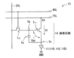
図2は、画素回路アレイ部13の回路構成の一例を表したものである。画素回路アレイ部13は、表示パネル10の表示領域に形成されている。画素回路アレイ部13は、例えば、図1、図2に示したように、行状に配置された複数の走査線WSLと、列状に配置された複数の信号線DTLと、走査線WSLに沿って行状に配置された複数の電源線PSLとを有している。各走査線WSLと各信号線DTLとの交差部に対応して、複数の有機EL素子11および画素回路14が行列状に配置(2次元配置)されている。画素回路14は、例えば、駆動トランジスタTr1、書き込みトランジスタTr2および保持容量Csによって構成されたものであり、2Tr1Cの回路構成となっている。駆動トランジスタTr1および書き込みトランジスタTr2は、例えば、nチャネルMOS型の薄膜トランジスタ(TFT(Thin Film Transistor))により形成されている。なお、TFTの種類は特に限定されるものではなく、例えば、逆スタガー構造(いわゆるボトムゲート型)であってもよいし、スタガー構造(トップゲート型)であってもよい。また、駆動トランジスタTr1または書き込みトランジスタTr2は、pチャネルMOS型のTFTであってもよい。
[Pixel circuit array section]
FIG. 2 illustrates an example of a circuit configuration of the pixel
画素回路アレイ部13において、各信号線DTLは、信号線駆動回路23の出力端(図示せず)と、書き込みトランジスタTr2のドレイン電極(図示せず)に接続されている。各走査線WSLは、走査線駆動回路24の出力端(図示せず)と、書き込みトランジスタTr2のゲート電極(図示せず)に接続されている。各電源線PSLは、電源線駆動回路25の出力端(図示せず)と、駆動トランジスタTr1のドレイン電極(図示せず)に接続されている。書き込みトランジスタTr2のソース電極(図示せず)は、駆動トランジスタTr1のゲート電極(図示せず)と、保持容量Csの一端に接続されている。駆動トランジスタTr1のソース電極(図示せず)と保持容量Csの他端とが、有機EL素子11のアノード電極(図示せず)に接続されている。有機EL素子11のカソード電極(図示せず)は、例えばグラウンド線GNDに接続されている。なお、カソード電極は、各有機EL素子11の共通電極として用いられており、例えば、表示パネル10の表示領域全体に渡って連続して形成され、平板状となっている。
In the pixel
[駆動回路]
次に、画素回路アレイ部13の周辺に設けられた駆動回路20内の各回路について、図1を参照して説明する。
[Drive circuit]
Next, each circuit in the
映像信号処理回路21は、外部から入力されたデジタルの映像信号20Aに対して所定の補正を行うと共に、補正した後の映像信号21Aを信号線駆動回路23に出力するようになっている。所定の補正としては、例えば、ガンマ補正や、オーバードライブ補正などが挙げられる。また、映像信号処理回路21は、映像信号20Aまたは映像信号21Aに基づいて、1フィールド期間における発光期間の比である発光期間と消光期間のデューティ比(発光期間/1フィールド期間×100)を決定するものである。具体的には、映像信号処理回路21は、例えば、映像信号20Aまたは映像信号21Aに基づいて、デューティ比を決定する消去パルス(後述)を出力するタイミングと、消去パルスを出力する信号線DTLを決定するものである。映像信号処理回路21は、例えば、決定されたタイミングおよび消去パルスを出力する信号線DTLを示す消去制御信号21Bを信号線駆動回路23に出力するようになっている。
The video
タイミング生成回路22は、信号線駆動回路23、走査線駆動回路24および電源線駆動回路25が連動して動作するように制御するものである。タイミング生成回路22は、例えば、外部から入力された同期信号20Bに応じて(同期して)、これらの回路に対して制御信号22Aを出力するようになっている。
The
信号線駆動回路23は、制御信号22Aの入力に応じて(同期して)、映像信号21Aに対応するアナログの映像信号を各信号線DTLに印加して、アナログの映像信号またはそれに対応する信号を選択対象の画素回路14に書き込むものである。具体的には、信号線駆動回路23は、映像信号21Aに対応する信号電圧Vsigを各信号線DTLに印加して、選択対象の画素回路14への書き込みを行うものである。なお、書き込みとは、駆動トランジスタTr1のゲートに所定の電圧を印加することを指している。
In response to (in synchronization with) the input of the
また、信号線駆動回路23は、制御信号22Aの入力に応じて(同期して)、映像信号処理回路21によって設定されたデューティ比の大きさに応じた選択電圧を各信号線に順次印加して、選択対象の画素回路への書き込みを行うものである。具体的には、信号線駆動回路23は、映像信号処理回路21から出力された消去制御信号21Bの入力に応じて、選択電圧として電圧Versを特定の信号線DTLに印加して、選択対象の画素回路14への書き込みを行うものである。言い換えると、信号線駆動回路23は、映像信号処理回路21から出力された消去制御信号21Bの入力に応じて、電圧をVsigからVersに立ち下げる消去パルスを特定の信号線DTLに印加して、選択対象の画素回路14への書き込みを行うものである。さらに、信号線駆動回路23は、映像信号処理回路21から出力された消去制御信号21Bの入力に応じて、選択電圧として電圧Vofsを特定の信号線DTLに印加して、選択対象の画素回路14への書き込みを行わないこともできる。
The signal
信号線駆動回路23は、例えば、信号電圧Vsigと、有機EL素子11の消光時に駆動トランジスタTr1のゲートに印加する電圧Vofs,Versとを出力することが可能となっている。ここで、電圧Vofsは、有機EL素子11の閾値電圧Velよりも低い電圧値(一定値)となっており、かつVM−Vth-WSよりも高い電圧値となっている。電圧Vofsは、消去制御信号21Bによって非消去が選択されたときに、後述の消去選択期間に信号線DTLに印加されるものでもある。
The signal
なお、電圧VMは、映像信号処理回路21によって消去が選択されたときに、後述の消去選択期間Tersに走査線WSLに印加される電圧(一定値)である。電圧VMは、電圧VLよりも高く、電圧VHよりも低い電圧値(一定値)となっている。電圧VLは、書き込みトランジスタTr2のオン電圧よりも低い電圧値(一定値)となっている。電圧VHは、書き込みトランジスタTr2のオン電圧以上の電圧値(一定値)となっている。電圧Vth-WSは、書き込みトランジスタTr2の閾値電圧である。電圧Versは、映像信号処理回路21によって消去が選択されたときに、後述の消去選択期間Tersに信号線DTLに印加されるものである。電圧Versは、VL−Vth-WSよりも高く、VM−Vth-WSよりも低い電圧値(一定値)となっている。
The voltage V M, when the erasing by the video
走査線駆動回路24は、制御信号22Aの入力に応じて(同期して)、複数の走査線WSLに選択パルスを順次印加して、複数の有機EL素子11および複数の画素回路14を順次選択するものである。また、走査線駆動回路24は、制御信号22Aの入力に応じて(同期して)、信号線DTLに上記選択電圧(電圧Vers)が印加されている時に、それ以外の期間に印加する選択パルスの波高値(電圧VH)のよりも小さな波高値(電圧VM)の選択パルスを走査線WSLに印加するものである。走査線駆動回路24は、例えば、書き込みトランジスタTr2をオンさせるときに印加する電圧VHと、書き込みトランジスタTr2をオンもしくはオフさせるかを選択するときに印加する電圧VMと、書き込みトランジスタTr2をオフさせるときに印加する電圧VLとを出力することが可能となっている。
The scanning
電源線駆動回路25は、制御信号22Aの入力に応じて(同期して)、複数の電源線PSLに制御パルスを順次印加して、有機EL素子11の発光および消光を制御するものである。電源線駆動回路25は、例えば、駆動トランジスタTr1に電流を流すときに印加する電圧VccHと、駆動トランジスタTr1に電流を流さないときに印加する電圧VccLとを出力することが可能となっている。ここで、電圧VccLは、有機EL素子11の閾値電圧Velと、有機EL素子11のカソードの電圧Vcaとを足し合わせた電圧(Vel+Vca)よりも低い電圧値(一定値)である。VccHは、電圧(Vel+Vca)以上の電圧値(一定値)である。
The power supply
(1.2 映像信号処理回路21の動作)
図3は、映像信号処理回路21における処理フローの一例を表したものである。映像信号処理回路21は、デューティ比を以下のようにして設定する。映像信号処理回路21は、例えば、図3に示したように、1フレーム期間TFを、消光期間Toff、発光選択期間Ton1、発光選択期間Ton2、発光選択期間Ton3、発光選択期間Ton4の5つに分ける。消光期間Toffとは、後述するように、Vth補正やμ補正などを行う期間でもある。次に、映像信号処理回路21は、例えば、図4に示したように、映像信号20Aまたは映像信号21Aの大きさに対応するデューティ比をモード1からモード4の中から1つ選択する。
(1.2 Operation of video signal processing circuit 21)
FIG. 3 shows an example of a processing flow in the video
ここで、モード1は、発光選択期間Ton1において「発光」を選択し、発光選択期間Ton2,Ton3,Ton4において「非発光」を選択するモードである。モード2は、発光選択期間Ton1,Ton2において「発光」を選択し、発光選択期間Ton3,Ton4においても「非発光」を選択するモードである。モード3は、発光選択期間Ton1,Ton2,Ton3において「発光」を選択し、発光選択期間Ton4において「非発光」を選択するモードである。モード4は、発光選択期間Ton1,Ton2,Ton3,Ton4において「発光」を選択するモードである。 Here, mode 1, select "luminescence" in the light-emitting selection period T on1, a mode for selecting the "non-light emission" in the light-emitting selection period T on2, T on3, T on4 . Mode 2, select "luminescence" in the light-emitting selection period T on1, T on2, even in the light-emitting selection period T on3, T on4 is a mode for selecting the "non-light emission." Mode 3 selects the "emission" in the light-emitting selection period T on1, T on2, T on3 , a mode for selecting the "non-light emission" in the light-emitting selection period T on4. Mode 4 is a mode for selecting the "light emission" in the light-emitting selection period T on1, T on2, T on3 , T on4.
次に、映像信号処理回路21は、信号線駆動回路23に対して、映像信号21Aを所定のタイミングで出力すると共に、モードに対応する消去制御信号21Bを所定のタイミングで出力する。なお、例えば、モード3に消去制御信号21Bが信号線駆動回路23に印加されると、信号線駆動回路23は、電圧Vofsを図5中の最初から3番目までの消去選択期間Tersに信号線DTLに印加すると共に、電圧Versを、図5中の4番目の消去選択期間Tersに信号線DTLに印加する。また、例えば、モード4に消去制御信号21Bが信号線駆動回路23に印加されると、信号線駆動回路23は、電圧Vofsを図6中の全ての消去選択期間Tersに信号線DTLに印加する。
Next, the video
(1.3 表示装置の動作)
図5は、表示装置1をモード3で駆動させたときの各種波形の一例を表したものである。図6は、表示装置1をモード4で駆動させたときの各種波形の一例を表したものである。図5(A)〜(C)、図6(A)〜(C)には、信号線DTLにVofs、Vsig、Versが周期的に印加され、走査線WSLにVH、VL、VMが所定のタイミングで印加され、電源線PSLにVccL、VccHが所定のタイミングで印加されている様子が示されている。図5(D),(E)、図6(D),(E)には、信号線DTL、走査線WSLおよび電源線PSLへの電圧印加に応じて、駆動トランジスタTr1のゲート電圧Vgおよびソース電圧Vsが時々刻々変化している様子が示されている。以下では、まず、モード共通の動作について説明したのち、個別のモードの動作について説明するものとする。
(1.3 Operation of display device)
FIG. 5 shows an example of various waveforms when the display device 1 is driven in the mode 3. FIG. 6 shows an example of various waveforms when the display device 1 is driven in the
[Vth補正準備期間]
まず、Vth補正の準備を行う。具体的には、電源線駆動回路25が電源線PSLの電圧をVccHからVccLに下げる(T1)。すると、ソース電圧VsがVccLとなり、有機EL素子11が消光すると共に、ゲート電圧VgがVofsに下がる。次に、信号線DTLの電圧がVofsとなっており、かつ電源線PSLの電圧がVccLとなっている間に、走査線駆動回路24が走査線WSLの電圧をVLからVHに上げる。
[V th correction preparation period]
First, preparation for V th correction is performed. Specifically, the power supply
[最初のVth補正期間]
次に、Vthの補正を行う。具体的には、信号線DTLの電圧がVofsとなっている間に、電源線駆動回路25が電源線PSLの電圧をVccLからVccHに上げる(T2)。すると、駆動トランジスタTr1のドレイン−ソース間に電流Idが流れ、ソース電圧Vsが上昇する。その後、信号線駆動回路23が信号線DTLの電圧をVofsからVsigに切り替える前に、走査線駆動回路24が走査線WSLの電圧をVHからVLに下げる(T3)。すると、駆動トランジスタTr1のゲートがフローティングとなり、Vthの補正が一旦停止する。
[First V th correction period]
Next, V th is corrected. Specifically, while the voltage of the signal line DTL is V ofs, the power supply
[最初のVth補正休止期間]
Vth補正が休止している期間中は、先のVth補正を行った行(画素)とは異なる他の行(画素)において、信号線DTLの電圧のサンプリングが行われる。なお、Vth補正が不十分である場合、すなわち、駆動トランジスタTr1のゲート−ソース間の電位差Vgsが駆動トランジスタTr1の閾値電圧Vthよりも大きい場合には、以下のようになる。すなわち、Vth補正休止期間中にも、先のVth補正を行った行(画素)において、駆動トランジスタTr1のドレイン−ソース間に電流Idsが流れ、ソース電圧Vsが上昇し、保持容量Csを介したカップリングによりゲート電圧Vgも上昇する。
[First V th correction pause period]
During the period in which the V th correction is paused, the voltage of the signal line DTL is sampled in another row (pixel) different from the row (pixel) on which the previous V th correction has been performed. In the case V th correction is insufficient, i.e., the gate of the drive transistor Tr 1 - when the potential difference V gs between the source is larger than the threshold voltage V th of the drive transistor Tr 1 is as follows. That is, even during the V th correction pause period, in the row (pixel) in which the previous V th correction is performed, the current I ds flows between the drain and source of the drive transistor Tr 1 , and the source voltage V s rises and is held. also it increases the gate voltage V g by the capacitive coupling C s.
[2回目のVth補正期間]
Vth補正休止期間が終了した後、Vthの補正を再び行う。具体的には、信号線DTLの電圧がVofsとなっており、Vth補正が可能となっている時に、走査線駆動回路24が走査線WSLの電圧をVLからVHに上げ(T4)、駆動トランジスタTr1のゲートを信号線DTLに接続する。このとき、ソース電圧Vsが(Vofs−Vth)よりも低い場合(Vth補正がまだ完了していない場合)には、駆動トランジスタTr1がカットオフするまで(電位差VgsがVthになるまで)、駆動トランジスタTr1のドレイン−ソース間に電流Idが流れる。その結果、保持容量CsがVthに充電され、電位差VgsがVthとなる。その後、信号線駆動回路23が信号線DTLの電圧をVofsからVsigに切り替える前に、走査線駆動回路24が走査線WSLの電圧をVHからVLに下げる(T5)。すると、駆動トランジスタTr1のゲートがフローティングとなるので、電位差Vgsを信号線DTLの電圧の大きさに拘わらずVthのままで維持することができる。このように、電位差VgsをVthに設定することにより、駆動トランジスタTr1の閾値電圧Vthが画素回路14ごとにばらついた場合であっても、有機EL素子11の発光輝度がばらつくのをなくすことができる。
[Second V th correction period]
After the V th correction pause period ends, the V th correction is performed again. Specifically, when the voltage of the signal line DTL is V ofs and V th correction is possible, the scanning
[2回目のVth補正休止期間]
その後、Vth補正の休止期間中に、信号線駆動回路23が信号線DTLの電圧をVofsからVsigに切り替える。
[Second V th correction pause period]
Thereafter, the signal
[書き込み・μ補正期間]
Vth補正休止期間が終了した後、書き込みとμ補正を行う。具体的には、信号線DTLの電圧がVsigとなっている間に、走査線駆動回路24が走査線WSLの電圧をVLからVHに上げ(T6)、駆動トランジスタTr1のゲートを信号線DTLに接続する。すると、駆動トランジスタTr1のゲート電圧がVsigとなる。このとき、有機EL素子11のアノード電圧はこの段階ではまだ有機EL素子11の閾値電圧Velよりも小さく、有機EL素子11はカットオフしている。そのため、電流Idsは有機EL素子11の素子容量(図示せず)に流れ、素子容量が充電されるので、ソース電圧VsがΔVだけ上昇し、やがて電位差VgsがVsig+Vth−ΔVとなる。このようにして、書き込みと同時にμ補正が行われる。ここで、駆動トランジスタTr1の移動度μが大きい程、ΔVも大きくなるので、電位差Vgsを発光前にΔVだけ小さくすることにより、画素回路14ごとの移動度μのばらつきを取り除くことができる。
[Writing / μ correction period]
After the end of the V th correction pause period, writing and μ correction are performed. Specifically, while the voltage of the signal line DTL is V sig , the scanning
[発光選択期間(Ton1)]
次に、走査線駆動回路24が走査線WSLの電圧をVHからVLに下げる(T7)。すると、駆動トランジスタTr1のゲートがフローティングとなり、駆動トランジスタTr1のゲート−ソース間の電圧Vgsを一定に維持した状態で、駆動トランジスタTr1のドレイン−ソース間に電流Idが流れる。その結果、ソース電圧Vsが上昇し、それに連動して駆動トランジスタTr1のゲートも上昇し、有機EL素子11が所望の輝度で発光する(T8)。
[Light emission selection period (T on1 )]
Next, the scanning
次に、図5を参照しつつ、モード3が選択されているときの動作について説明する。 Next, the operation when mode 3 is selected will be described with reference to FIG.
[発光選択期間(Ton1)]
有機EL素子11が発光し始めてから所定の期間が経過したところで、信号線駆動回路23が、消去制御信号21Bの印加に対応して、信号線DTLの電圧をVsigからVofsに下げて、1回目の消去選択期間Tersに入る(T8)。続いて、走査線駆動回路24が走査線WSLの電圧をVLからVMに上げる(T9)。このとき、書き込みトランジスタTr2のゲート−ソース間の電圧Vgsは、VM−Vofsであり、書き込みトランジスタTr2の閾値電圧Vth wsよりも小さい。従って、書き込みトランジスタTr2はオフしたままであり、駆動トランジスタTr1のゲートがフローティング状態を維持しているので、有機EL素子11の発光が継続する。その後、信号線DTLの電圧がVofsとなっている間に、走査線駆動回路24が走査線WSLの電圧をVMからVLに下げる。このときも、書き込みトランジスタTr2はオフしたままであり、駆動トランジスタTr1のゲートがフローティング状態を維持しているので、引き続き、有機EL素子11の発光が継続する。その後、信号線駆動回路23が、信号線DTLの電圧をVofsからVsigに上げる。
[Light emission selection period (T on1 )]
When a predetermined period has elapsed since the organic EL element 11 started to emit light, the signal
[発光選択期間(Ton2,Ton3)]
これ以降、発光選択期間(Ton2,Ton3)においては、上記のステップが繰り返され、有機EL素子11の発光が継続した状態で、2回目,3回目の消去選択期間Tersが経過する。
[Emitting selection period (T on2, T on3)]
Thereafter, in the light emitting selection period (T on2, T on3), the above steps are repeated, in a state in which light is continued in the organic EL element 11, a second time, the third erase selection period T ers elapses.
[発光選択期間(Ton4)]
次に、信号線駆動回路23が、消去制御信号21Bの印加に対応して、信号線DTLの電圧をVsigからVersに下げて、4回目の消去選択期間Tersに入る(T8)。今回の消去選択期間Tersでは、信号線DTLの電圧がVersとなっており、有機EL素子11の非発光が選択されている。つまり、映像信号20Aまたは映像信号21Aに基づいて決定されたデューティ比となるように、発光選択期間(Ton4)の開始のタイミングで特定の信号線DTLに消去パルス(電圧Vsigから電圧Versへの立ち下がり信号)が印加される。続いて、走査線駆動回路24が走査線WSLの電圧をVLからVMに上げる(T9)。すると、駆動トランジスタTr1のゲートが信号線DTLに接続され、駆動トランジスタTr1のゲート電圧がVersとなり、駆動トランジスタTr1のゲート−ソース間の電圧VgsがVers−Vel<Vthとなるので、有機EL素子11の発光が停止する。つまり、信号線駆動回路23は、消去制御信号21Bの印加に対応して、4回目の消去選択期間Tersに電圧Versを信号線DTLに印加して、選択対象の有機EL素子11に流れる定常電流を停止する。その後、信号線DTLの電圧がVersとなっている間に、走査線駆動回路24が走査線WSLの電圧をVMからVLに下げる。すると、駆動トランジスタTr1のゲートがフローティングとなるので、その後、引き続き、有機EL素子11の発光は停止したままとなる。
[Light emission selection period (T on4 )]
Next, the signal
本実施の形態の表示装置1では、上記のようにして、各画素12において画素回路14がオンオフ制御され、各画素12の有機EL素子11に駆動電流が注入されることにより、正孔と電子とが再結合して発光が起こる。この光は、陽極と陰極との間で多重反射し、陰極等を透過して外部に取り出される。その結果、表示パネル10において画像が表示される。
In the display device 1 of the present embodiment, as described above, the
(1.4 作用・効果) (1.4 Action / effect)
ところで、従来の有機EL表示装置では、一般に、1フレーム期間内に有機EL素子の発光、消光を行うに際して、1フィールド期間における発光期間の比である発光期間と消光期間のデューティ比(発光期間/1フィールド期間×100)が全画素一定となる。そのため、階調数を増やそうとした場合には、信号線に印加可能な電圧値を増やすことになる。しかし、そのようにした場合には、階調間の電圧値の差が小さくなり、階調制御が困難となる。 By the way, in the conventional organic EL display device, in general, when the organic EL element emits and extinguishes within one frame period, the duty ratio of the light emitting period to the extinction period (light emitting period / One field period × 100) is constant for all pixels. Therefore, when an attempt is made to increase the number of gradations, the voltage value that can be applied to the signal line is increased. However, in such a case, the voltage value difference between gradations becomes small, and gradation control becomes difficult.
一方、本実施の形態では、映像信号21Aに対応する信号電圧Vsigが各信号線DTLに印加されて、選択対象の画素回路14への書き込みが行われる。また、映像信号20Aまたは映像信号21Aに基づいて決定されたデューティ比となるように所定のタイミングで特定の信号線DTLに消去パルス(電圧Vers)が印加される。さらに、特定の信号線DTLに消去パルス(電圧Vers)が印加されている時に、特定の信号線DTLに対応する画素回路14内の駆動トランジスタTr1のゲート−ソース間の電圧VgsがVthを下回るように、走査線WSLの電圧がVLからVMに上げられる。これにより、特定の画素12内の有機EL素子11の発光が停止する。これにより、信号電圧Vsigの波高値を画素12ごとに設定することができるだけでなく、デューティ比も画素12ごとに設定することができる。従って、上記の場合と比べて、階調制御が容易である。
On the other hand, in the present embodiment, the signal voltage V sig corresponding to the
<2.モジュールおよび適用例>
以下、上述した実施の形態で説明した表示装置の適用例について説明する。上記実施の形態の表示装置は、テレビジョン装置、デジタルカメラ、ノート型パーソナルコンピュータ、携帯電話等の携帯端末装置あるいはビデオカメラなど、外部から入力された映像信号あるいは内部で生成した映像信号を、画像あるいは映像として表示するあらゆる分野の電子機器の表示装置に適用することが可能である。
<2. Modules and application examples>
Hereinafter, application examples of the display device described in the above embodiment will be described. The display device of the above embodiment is a television device, a digital camera, a notebook personal computer, a mobile terminal device such as a mobile phone, or a video camera, and the like. Alternatively, the present invention can be applied to display devices for electronic devices in various fields that display images.
(モジュール)
上記実施の形態の表示装置1は、例えば、図7に示したようなモジュールとして、後述する適用例1〜5などの種々の電子機器に組み込まれる。このモジュールは、例えば、基板31の一辺に、封止用基板32から露出した領域210を設け、この露出した領域210に、駆動回路20の配線を延長して外部接続端子(図示せず)を形成したものである。外部接続端子には、信号の入出力のためのフレキシブルプリント配線基板(FPC;Flexible Printed Circuit)220が設けられていてもよい。
(module)
The display device 1 according to the above-described embodiment is incorporated into various electronic devices such as application examples 1 to 5 described later, for example, as a module as illustrated in FIG. In this module, for example, a
(適用例1)
図8は、上記実施の形態の表示装置1が適用されるテレビジョン装置の外観を表したものである。このテレビジョン装置は、例えば、フロントパネル310およびフィルターガラス320を含む映像表示画面部300を有しており、この映像表示画面部300は、上記各実施の形態に係る表示装置1により構成されている。
(Application example 1)
FIG. 8 illustrates an appearance of a television device to which the display device 1 of the above embodiment is applied. The television apparatus has, for example, a video display screen unit 300 including a front panel 310 and a filter glass 320. The video display screen unit 300 is configured by the display device 1 according to each of the above embodiments. Yes.
(適用例2)
図9は、上記実施の形態の表示装置1が適用されるデジタルカメラの外観を表したものである。このデジタルカメラは、例えば、フラッシュ用の発光部410、表示部420、メニュースイッチ430およびシャッターボタン440を有しており、その表示部420は、上記実施の形態に係る表示装置1により構成されている。
(Application example 2)
FIG. 9 shows the appearance of a digital camera to which the display device 1 of the above embodiment is applied. The digital camera includes, for example, a flash light emitting unit 410, a display unit 420, a menu switch 430, and a
(適用例3)
図10は、上記実施の形態の表示装置1が適用されるノート型パーソナルコンピュータの外観を表したものである。このノート型パーソナルコンピュータは、例えば、本体510,文字等の入力操作のためのキーボード520および画像を表示する表示部530を有しており、その表示部530は、上記各実施の形態に係る表示装置1により構成されている。
(Application example 3)
FIG. 10 shows the appearance of a notebook personal computer to which the display device 1 of the above embodiment is applied. The notebook personal computer has, for example, a main body 510, a keyboard 520 for inputting characters and the like, and a display unit 530 for displaying an image. The display unit 530 is a display according to each of the above embodiments. The apparatus 1 is configured.
(適用例4)
図11は、上記実施の形態の表示装置1が適用されるビデオカメラの外観を表したものである。このビデオカメラは、例えば、本体部610,この本体部610の前方側面に設けられた被写体撮影用のレンズ620,撮影時のスタート/ストップスイッチ630および表示部640を有しており、その表示部640は、上記各実施の形態に係る表示装置1により構成されている。
(Application example 4)
FIG. 11 shows the appearance of a video camera to which the display device 1 of the above embodiment is applied. This video camera has, for example, a main body 610, a subject photographing lens 620 provided on the front side surface of the main body 610, a start /
(適用例5)
図12は、上記実施の形態の表示装置1が適用される携帯電話機の外観を表したものである。この携帯電話機は、例えば、上側筐体710と下側筐体720とを連結部(ヒンジ部)730で連結したものであり、ディスプレイ740,サブディスプレイ750,ピクチャーライト760およびカメラ770を有している。そのディスプレイ740またはサブディスプレイ750は、上記各実施の形態に係る表示装置1により構成されている。
(Application example 5)
FIG. 12 shows the appearance of a mobile phone to which the display device 1 of the above embodiment is applied. For example, the mobile phone is obtained by connecting an
以上、実施の形態および適用例を挙げて本発明を説明したが、本発明は上記実施の形態等に限定されるものではなく、種々変形が可能である。 While the present invention has been described with the embodiment and application examples, the present invention is not limited to the above-described embodiment and the like, and various modifications can be made.
例えば、上記実施の形態等では、表示装置1がアクティブマトリクス型である場合について説明したが、アクティブマトリクス駆動のための画素回路14の構成は上記実施の形態等で説明したものに限られず、必要に応じて容量素子やトランジスタを画素回路14に追加してもよい。その場合、画素回路14の変更に応じて、上述した信号線駆動回路23、走査線駆動回路24、電源線駆動回路25のほかに、必要な駆動回路を追加してもよい。
For example, in the above-described embodiment, the case where the display device 1 is an active matrix type has been described. However, the configuration of the
また、上記実施の形態等では、信号線駆動回路23、走査線駆動回路24、電源線駆動回路25の駆動をタイミング制御回路22が制御していたが、他の回路がこれらの駆動を制御するようにしてもよい。また、信号線駆動回路23、走査線駆動回路24、電源線駆動回路25の制御は、ハードウェア(回路)で行われていてもよいし、ソフトウェア(プログラム)で行われていてもよい。
In the above embodiment and the like, the
また、上記実施の形態等では、画素回路14が、2Tr1Cの回路構成となっていたが、トランジスタが有機EL素子11に直列に接続された回路構成を含んでいるものであれば、2Tr1Cの回路構成以外の回路構成となっていてもよい。
In the above-described embodiment and the like, the
また、上記実施の形態等では、駆動トランジスタTr1,書き込みトランジスタTr2は、nチャネルMOS型の薄膜トランジスタ(TFT(Thin Film Transistor))により形成されている場合が例示されていたが、pチャネルトランジスタ(例えばpチャネルMOS型のTFT)により形成されていてもよい。ただし、その場合には、トランジスタTr2のソースおよびドレインのうち電源線PSLと未接続の方と保持容量Csの他端とを有機EL素子11のカソードに接続し、有機EL素子11のアノードをGNDなどに接続することが好ましい。 Further, in the above-described embodiment and the like, the case where the drive transistor Tr 1 and the write transistor Tr 2 are formed by n-channel MOS thin film transistors (TFTs) is illustrated, but a p-channel transistor is exemplified. (For example, a p-channel MOS type TFT) may be used. However, in this case, the source and drain of the transistor Tr 2 that are not connected to the power supply line PSL and the other end of the storage capacitor C s are connected to the cathode of the organic EL element 11 and the anode of the organic EL element 11 is connected. Is preferably connected to GND or the like.
1…表示装置、10…表示パネル、11,11R,11G,11B…有機EL素子、12…画素、13…画素回路アレイ部、14…画素回路、20…駆動回路、21…映像信号処理回路、20A,21A…映像信号、20B…同期信号、21B…消去制御信号、22…タイミング生成回路、22A…制御信号、23…信号線駆動回路、24…走査線駆動回路、25…電源線駆動回路、Cs…保持容量、DTL…信号線、Id…電流、GND…グラウンド線、PSL…電源線、Tr1…駆動トランジスタ、Tr2…書き込みトランジスタ、Vg…ゲート電圧、Vgs…ゲート−ソース間電圧、Vs…ソース電圧、Vth…閾値電圧、WSL…走査線。 DESCRIPTION OF SYMBOLS 1 ... Display apparatus, 10 ... Display panel, 11, 11R, 11G, 11B ... Organic EL element, 12 ... Pixel, 13 ... Pixel circuit array part, 14 ... Pixel circuit, 20 ... Drive circuit, 21 ... Video signal processing circuit, 20A, 21A ... Video signal, 20B ... Synchronization signal, 21B ... Erase control signal, 22 ... Timing generation circuit, 22A ... Control signal, 23 ... Signal line drive circuit, 24 ... Scan line drive circuit, 25 ... Power line drive circuit, C s : holding capacitor, DTL ... signal line, I d ... current, GND ... ground line, PSL ... power supply line, Tr 1 ... drive transistor, Tr 2 ... write transistor, V g ... gate voltage, V gs ... gate-source during voltage, V s ... source voltage, V th ... threshold voltage, WSL ... scan line.
Claims (3)
映像信号に対応する信号電圧を各信号線に順次印加すると共に、前記映像信号に基づいて決定されたデューティ比となるように所定のタイミングで特定の信号線に消去パルスを印加する信号線駆動回路と、
前記特定の信号線に前記消去パルスが印加されている時に、選択パルスを前記走査線に印加する走査線駆動回路と
を備え、
前記画素回路は、前記発光素子に接続された駆動トランジスタと、前記駆動トランジスタのゲートおよび前記信号線に接続された書き込みトランジスタと、前記駆動トランジスタのゲート・ソース間電圧を保持する保持容量とを含み、
前記選択パルスは、前記消去パルスが前記信号線に印加されている時に、当該選択パルスが前記走査線に印加されたとき、前記書き込みトランジスタがオンする電圧値となっており、
前記選択パルスは、さらに、前記発光素子の閾値電圧よりも低い電圧であって、かつ当該選択パルスの波高値から前記書き込みトランジスタの閾値電圧を減算することにより得られる値よりも高い電圧が前記信号線に印加されるとともに、当該選択パルスが前記走査線に印加されている時、前記書き込みトランジスタがオフしている電圧値となっている
表示装置。 A pixel circuit array unit including a plurality of scanning lines arranged in a row, a plurality of signal lines arranged in a column, a plurality of light emitting elements and a plurality of pixel circuits arranged in a matrix;
A signal line driving circuit that sequentially applies a signal voltage corresponding to a video signal to each signal line and applies an erasing pulse to a specific signal line at a predetermined timing so as to have a duty ratio determined based on the video signal When,
When the erase pulse is applied to the specific signal line, and a scanning line driving circuit for applying a select pulse to the scan lines,
The pixel circuit includes a drive transistor connected to the light emitting element, a write transistor connected to the gate of the drive transistor and the signal line, and a storage capacitor for holding a gate-source voltage of the drive transistor. ,
The selection pulse has a voltage value that turns on the writing transistor when the erasing pulse is applied to the signal line and the selection pulse is applied to the scanning line.
The selection pulse further has a voltage lower than a threshold voltage of the light emitting element, and a voltage higher than a value obtained by subtracting the threshold voltage of the writing transistor from the peak value of the selection pulse. A display device having a voltage value at which the writing transistor is turned off when the selection pulse is applied to the scanning line while being applied to the line .
映像信号に対応する信号電圧を各信号線に順次印加すると共に、前記映像信号に基づいて決定されたデューティ比となるように所定のタイミングで特定の信号線に消去パルスを印加するステップと、
前記特定の信号線に前記消去パルスが印加されている時に、選択パルスを前記走査線に印加するステップと
を含み、
前記画素回路が、前記発光素子に接続された駆動トランジスタと、前記駆動トランジスタのゲートおよび前記信号線に接続された書き込みトランジスタと、前記駆動トランジスタのゲート・ソース間電圧を保持する保持容量とを含み、
前記選択パルスは、前記消去パルスが前記信号線に印加されている時に、当該選択パルスが前記走査線に印加されたとき、前記書き込みトランジスタがオンする電圧値となっており、
前記選択パルスは、さらに、前記発光素子の閾値電圧よりも低い電圧であって、かつ当該選択パルスの波高値から前記書き込みトランジスタの閾値電圧を減算することにより得られる値よりも高い電圧が前記信号線に印加されるとともに、当該選択パルスが前記走査線に印加されている時、前記書き込みトランジスタがオフしている電圧値となっている
表示装置の駆動方法。 A pixel circuit array unit including a plurality of scanning lines arranged in rows, a plurality of signal lines arranged in columns, a plurality of light emitting elements and a plurality of pixel circuits arranged in a matrix, and the pixel circuit Preparing a display device including a drive circuit for driving the array unit;
Applying a signal voltage corresponding to a video signal sequentially to each signal line, and applying an erasing pulse to a specific signal line at a predetermined timing so as to have a duty ratio determined based on the video signal;
When the erase pulse is applied to the specific signal line, it viewed including the steps of applying a selected pulse to the scan lines,
The pixel circuit includes a drive transistor connected to the light emitting element, a write transistor connected to the gate of the drive transistor and the signal line, and a storage capacitor that holds a gate-source voltage of the drive transistor. ,
The selection pulse has a voltage value that turns on the writing transistor when the erasing pulse is applied to the signal line and the selection pulse is applied to the scanning line.
The selection pulse further has a voltage lower than a threshold voltage of the light emitting element, and a voltage higher than a value obtained by subtracting the threshold voltage of the writing transistor from the peak value of the selection pulse. And a display device driving method in which when the selection pulse is applied to the scanning line, the writing transistor is turned off when the selection pulse is applied to the scanning line .
前記表示装置は、
行状に配置された複数の走査線と、列状に配置された複数の信号線と、行列状に配置された複数の発光素子および複数の画素回路とを含む画素回路アレイ部と、
映像信号に対応する信号電圧を各信号線に順次印加すると共に、前記映像信号に基づいて決定されたデューティ比となるように所定のタイミングで特定の信号線に消去パルスを印加する信号線駆動回路と、
前記特定の信号線に前記消去パルスが印加されている時に、選択パルスを前記走査線に印加する走査線駆動回路と
を有し、
前記画素回路は、前記発光素子に接続された駆動トランジスタと、前記駆動トランジスタのゲートおよび前記信号線に接続された書き込みトランジスタと、前記駆動トランジスタのゲート・ソース間電圧を保持する保持容量とを含み、
前記選択パルスは、前記消去パルスが前記信号線に印加されている時に、当該選択パルスが前記走査線に印加されたとき、前記書き込みトランジスタがオンする電圧値となっており、
前記選択パルスは、さらに、前記発光素子の閾値電圧よりも低い電圧であって、かつ当該選択パルスの波高値から前記書き込みトランジスタの閾値電圧を減算することにより得られる値よりも高い電圧が前記信号線に印加されるとともに、当該選択パルスが前記走査線に印加されている時、前記書き込みトランジスタがオフしている電圧値となっている
電子機器。 A display device,
The display device
A pixel circuit array unit including a plurality of scanning lines arranged in a row, a plurality of signal lines arranged in a column, a plurality of light emitting elements and a plurality of pixel circuits arranged in a matrix;
A signal line driving circuit that sequentially applies a signal voltage corresponding to a video signal to each signal line and applies an erasing pulse to a specific signal line at a predetermined timing so as to have a duty ratio determined based on the video signal When,
When the erase pulse is applied to the specific signal line, it has a scanning line driving circuit for applying a select pulse to the scan lines,
The pixel circuit includes a drive transistor connected to the light emitting element, a write transistor connected to the gate of the drive transistor and the signal line, and a storage capacitor for holding a gate-source voltage of the drive transistor. ,
The selection pulse has a voltage value that turns on the writing transistor when the erasing pulse is applied to the signal line and the selection pulse is applied to the scanning line.
The selection pulse further has a voltage lower than a threshold voltage of the light emitting element, and a voltage higher than a value obtained by subtracting the threshold voltage of the writing transistor from the peak value of the selection pulse. And an electronic device having a voltage value at which the writing transistor is turned off when the selection pulse is applied to the scanning line .
Priority Applications (4)
| Application Number | Priority Date | Filing Date | Title |
|---|---|---|---|
| JP2009165378A JP5282970B2 (en) | 2009-07-14 | 2009-07-14 | Display device, driving method thereof, and electronic apparatus |
| KR1020100064743A KR101611625B1 (en) | 2009-07-14 | 2010-07-06 | Display unit, method of driving the same, and electronics device |
| CN201010219661.5A CN101958101B (en) | 2009-07-14 | 2010-07-07 | Display unit, method of driving the same, and electronics device |
| US12/831,677 US8988322B2 (en) | 2009-07-14 | 2010-07-07 | Display unit with gradation control, method of driving the same, and electronics device |
Applications Claiming Priority (1)
| Application Number | Priority Date | Filing Date | Title |
|---|---|---|---|
| JP2009165378A JP5282970B2 (en) | 2009-07-14 | 2009-07-14 | Display device, driving method thereof, and electronic apparatus |
Publications (3)
| Publication Number | Publication Date |
|---|---|
| JP2011022240A JP2011022240A (en) | 2011-02-03 |
| JP2011022240A5 JP2011022240A5 (en) | 2012-08-30 |
| JP5282970B2 true JP5282970B2 (en) | 2013-09-04 |
Family
ID=43465037
Family Applications (1)
| Application Number | Title | Priority Date | Filing Date |
|---|---|---|---|
| JP2009165378A Active JP5282970B2 (en) | 2009-07-14 | 2009-07-14 | Display device, driving method thereof, and electronic apparatus |
Country Status (4)
| Country | Link |
|---|---|
| US (1) | US8988322B2 (en) |
| JP (1) | JP5282970B2 (en) |
| KR (1) | KR101611625B1 (en) |
| CN (1) | CN101958101B (en) |
Families Citing this family (3)
| Publication number | Priority date | Publication date | Assignee | Title |
|---|---|---|---|---|
| US9881554B2 (en) | 2015-02-11 | 2018-01-30 | Boe Technology Group Co., Ltd. | Driving method of pixel circuit and driving device thereof |
| CN104599637A (en) * | 2015-02-11 | 2015-05-06 | 京东方科技集团股份有限公司 | Pixel circuit drive method and drive device |
| CN105513528B (en) * | 2016-02-04 | 2018-06-22 | 京东方科技集团股份有限公司 | Capacitor compensating circuit, display base plate, display device and capacitance compensation method |
Family Cites Families (24)
| Publication number | Priority date | Publication date | Assignee | Title |
|---|---|---|---|---|
| US4975691A (en) * | 1987-06-16 | 1990-12-04 | Interstate Electronics Corporation | Scan inversion symmetric drive |
| US5095377A (en) * | 1990-08-02 | 1992-03-10 | Matsushita Electric Industrial Co., Ltd. | Method of driving a ferroelectric liquid crystal matrix panel |
| JP2808380B2 (en) * | 1992-04-17 | 1998-10-08 | 松下電器産業株式会社 | Driving method of spatial light modulator |
| JP3286503B2 (en) * | 1994-09-28 | 2002-05-27 | キヤノン株式会社 | Driving method of liquid crystal element and liquid crystal device using the driving method |
| US6417828B1 (en) * | 1999-02-18 | 2002-07-09 | Canon Kabushiki Kaisha | Liquid crystal composition, liquid crystal device, driving method thereof and liquid crystal apparatus |
| JP4092857B2 (en) * | 1999-06-17 | 2008-05-28 | ソニー株式会社 | Image display device |
| JP2001255509A (en) * | 2000-03-09 | 2001-09-21 | Sharp Corp | Smectic liquid crystal optical device |
| JP3838063B2 (en) * | 2000-09-29 | 2006-10-25 | セイコーエプソン株式会社 | Driving method of organic electroluminescence device |
| US6882330B2 (en) * | 2001-03-26 | 2005-04-19 | Lg Electronics Inc. | Field emission displaying device and driving method thereof |
| JP3714324B2 (en) * | 2002-12-24 | 2005-11-09 | コニカミノルタホールディングス株式会社 | Liquid crystal display device |
| US7928945B2 (en) | 2003-05-16 | 2011-04-19 | Semiconductor Energy Laboratory Co., Ltd. | Display device and driving method thereof |
| TWI254898B (en) * | 2003-10-02 | 2006-05-11 | Pioneer Corp | Display apparatus with active matrix display panel and method for driving same |
| CN100468498C (en) * | 2004-03-30 | 2009-03-11 | 富士胶片株式会社 | Light emission panel display device |
| JP2006003752A (en) * | 2004-06-18 | 2006-01-05 | Casio Comput Co Ltd | Display device and its driving control method |
| WO2006046553A1 (en) * | 2004-10-28 | 2006-05-04 | Matsushita Electric Industrial Co., Ltd. | Display and display driving method |
| KR100885573B1 (en) * | 2004-12-27 | 2009-02-24 | 교세라 가부시키가이샤 | Image display and its driving method, and driving method of electronic apparatus |
| FR2882457B1 (en) * | 2005-02-21 | 2007-09-21 | Commissariat Energie Atomique | PIXEL ADDRESSING CIRCUIT AND METHOD FOR CONTROLLING SUCH CIRCUIT |
| JP2008009391A (en) | 2006-06-02 | 2008-01-17 | Semiconductor Energy Lab Co Ltd | Display device and driving method thereof |
| WO2008018113A1 (en) * | 2006-08-07 | 2008-02-14 | Pioneer Corporation | Pixel driving apparatus and pixel driving method |
| KR100921506B1 (en) * | 2007-04-24 | 2009-10-13 | 한양대학교 산학협력단 | Display and method of driving the same |
| JP4470960B2 (en) * | 2007-05-21 | 2010-06-02 | ソニー株式会社 | Display device, driving method thereof, and electronic apparatus |
| JP4978435B2 (en) * | 2007-11-14 | 2012-07-18 | ソニー株式会社 | Display device, display device driving method, and electronic apparatus |
| JP2009128404A (en) * | 2007-11-20 | 2009-06-11 | Sony Corp | Display device, driving method of display device, and electronic equipment |
| JP5183336B2 (en) * | 2008-07-15 | 2013-04-17 | 富士フイルム株式会社 | Display device |
-
2009
- 2009-07-14 JP JP2009165378A patent/JP5282970B2/en active Active
-
2010
- 2010-07-06 KR KR1020100064743A patent/KR101611625B1/en active IP Right Grant
- 2010-07-07 US US12/831,677 patent/US8988322B2/en not_active Expired - Fee Related
- 2010-07-07 CN CN201010219661.5A patent/CN101958101B/en active Active
Also Published As
| Publication number | Publication date |
|---|---|
| US8988322B2 (en) | 2015-03-24 |
| US20110013100A1 (en) | 2011-01-20 |
| JP2011022240A (en) | 2011-02-03 |
| CN101958101B (en) | 2014-01-29 |
| KR101611625B1 (en) | 2016-04-11 |
| CN101958101A (en) | 2011-01-26 |
| KR20110006610A (en) | 2011-01-20 |
Similar Documents
| Publication | Publication Date | Title |
|---|---|---|
| JP5804732B2 (en) | Driving method, display device, and electronic apparatus | |
| JP2011112723A (en) | Display device, method of driving the same and electronic equipment | |
| JP2011112724A (en) | Display device, method of driving the same and electronic equipment | |
| JP2011112722A (en) | Display device, method of driving the same and electronic equipment | |
| TWI464725B (en) | Pixel circuit, display device, method of driving the display device, and electronic unit | |
| TWI409755B (en) | Display device and its driving method and electronic machine | |
| JP2009157019A (en) | Display device and electronic equipment | |
| JP2010243938A (en) | Display and method of driving the same | |
| JP2011022462A (en) | Display device, driving method therefor, and electronics device | |
| JP5577719B2 (en) | Display device, driving method thereof, and electronic apparatus | |
| JP2011128442A (en) | Display panel, display device and electronic equipment | |
| JP5321304B2 (en) | Display device, driving method thereof, and electronic apparatus | |
| KR101544212B1 (en) | Display apparatus driving method for display apparatus and electronic apparatus | |
| JP5282970B2 (en) | Display device, driving method thereof, and electronic apparatus | |
| JP5793058B2 (en) | Display panel, display device and electronic device | |
| JP2011145531A (en) | Display device, method for driving the same, and electronic equipment | |
| JP2011022239A (en) | Display device, method of driving the same, and electronic device | |
| JP5239812B2 (en) | Display device, display device driving method, and electronic apparatus | |
| JP2010014748A (en) | Display device and electronic apparatus | |
| JP2013122481A (en) | Display device, drive method therefor, and electronic device | |
| JP2011145394A (en) | Display device, method for driving the same, and electronic equipment | |
| JP2011154200A (en) | Display device, method for driving the same, and electronic equipment | |
| JP2011150079A (en) | Display device, method for driving the same, and electronic equipment | |
| JP2011102932A (en) | Display device and method of driving the same, electronic equipment, and display panel | |
| JP5168116B2 (en) | Display device, display device driving method, and electronic apparatus |
Legal Events
| Date | Code | Title | Description |
|---|---|---|---|
| A521 | Request for written amendment filed |
Free format text: JAPANESE INTERMEDIATE CODE: A523 Effective date: 20120710 |
|
| A621 | Written request for application examination |
Free format text: JAPANESE INTERMEDIATE CODE: A621 Effective date: 20120710 |
|
| A977 | Report on retrieval |
Free format text: JAPANESE INTERMEDIATE CODE: A971007 Effective date: 20130306 |
|
| A131 | Notification of reasons for refusal |
Free format text: JAPANESE INTERMEDIATE CODE: A131 Effective date: 20130314 |
|
| A521 | Request for written amendment filed |
Free format text: JAPANESE INTERMEDIATE CODE: A523 Effective date: 20130408 |
|
| TRDD | Decision of grant or rejection written | ||
| A01 | Written decision to grant a patent or to grant a registration (utility model) |
Free format text: JAPANESE INTERMEDIATE CODE: A01 Effective date: 20130502 |
|
| A61 | First payment of annual fees (during grant procedure) |
Free format text: JAPANESE INTERMEDIATE CODE: A61 Effective date: 20130515 |
|
| R151 | Written notification of patent or utility model registration |
Ref document number: 5282970 Country of ref document: JP Free format text: JAPANESE INTERMEDIATE CODE: R151 |
|
| S111 | Request for change of ownership or part of ownership |
Free format text: JAPANESE INTERMEDIATE CODE: R313111 |
|
| R350 | Written notification of registration of transfer |
Free format text: JAPANESE INTERMEDIATE CODE: R350 |
|
| R250 | Receipt of annual fees |
Free format text: JAPANESE INTERMEDIATE CODE: R250 |
|
| R250 | Receipt of annual fees |
Free format text: JAPANESE INTERMEDIATE CODE: R250 |
|
| R250 | Receipt of annual fees |
Free format text: JAPANESE INTERMEDIATE CODE: R250 |
|
| R250 | Receipt of annual fees |
Free format text: JAPANESE INTERMEDIATE CODE: R250 |
|
| R250 | Receipt of annual fees |
Free format text: JAPANESE INTERMEDIATE CODE: R250 |
|
| R250 | Receipt of annual fees |
Free format text: JAPANESE INTERMEDIATE CODE: R250 |
|
| R250 | Receipt of annual fees |
Free format text: JAPANESE INTERMEDIATE CODE: R250 |
|
| S303 | Written request for registration of pledge or change of pledge |
Free format text: JAPANESE INTERMEDIATE CODE: R316303 |
|
| R350 | Written notification of registration of transfer |
Free format text: JAPANESE INTERMEDIATE CODE: R350 |
|
| R250 | Receipt of annual fees |
Free format text: JAPANESE INTERMEDIATE CODE: R250 |
|
| S803 | Written request for registration of cancellation of provisional registration |
Free format text: JAPANESE INTERMEDIATE CODE: R316803 |
|
| R350 | Written notification of registration of transfer |
Free format text: JAPANESE INTERMEDIATE CODE: R350 |