JP5280440B2 - Conformal doping using high neutral density plasma implantation - Google Patents
Conformal doping using high neutral density plasma implantation Download PDFInfo
- Publication number
- JP5280440B2 JP5280440B2 JP2010514994A JP2010514994A JP5280440B2 JP 5280440 B2 JP5280440 B2 JP 5280440B2 JP 2010514994 A JP2010514994 A JP 2010514994A JP 2010514994 A JP2010514994 A JP 2010514994A JP 5280440 B2 JP5280440 B2 JP 5280440B2
- Authority
- JP
- Japan
- Prior art keywords
- plasma
- film
- substrate
- adsorbed
- ions
- Prior art date
- Legal status (The legal status is an assumption and is not a legal conclusion. Google has not performed a legal analysis and makes no representation as to the accuracy of the status listed.)
- Expired - Fee Related
Links
Images

Classifications
-
- H—ELECTRICITY
- H01—ELECTRIC ELEMENTS
- H01J—ELECTRIC DISCHARGE TUBES OR DISCHARGE LAMPS
- H01J37/00—Discharge tubes with provision for introducing objects or material to be exposed to the discharge, e.g. for the purpose of examination or processing thereof
- H01J37/32—Gas-filled discharge tubes
- H01J37/32009—Arrangements for generation of plasma specially adapted for examination or treatment of objects, e.g. plasma sources
- H01J37/32321—Discharge generated by other radiation
- H01J37/32339—Discharge generated by other radiation using electromagnetic radiation
-
- H—ELECTRICITY
- H01—ELECTRIC ELEMENTS
- H01J—ELECTRIC DISCHARGE TUBES OR DISCHARGE LAMPS
- H01J37/00—Discharge tubes with provision for introducing objects or material to be exposed to the discharge, e.g. for the purpose of examination or processing thereof
- H01J37/32—Gas-filled discharge tubes
- H01J37/32009—Arrangements for generation of plasma specially adapted for examination or treatment of objects, e.g. plasma sources
- H01J37/32412—Plasma immersion ion implantation
Description
ここで使用する項目見出しは文書構成目的のみであり、本願に記載される発明の要旨を限定するものとして理解されるべきでない。 The item headings used here are for document construction purposes only and should not be understood as limiting the gist of the invention described herein.
(発明の背景)(Background of the Invention)
本発明は半導体製造のためのプラズマ注入処理に関する。 The present invention relates to a plasma injection process for semiconductor manufacturing.
プラズマ処理は数十年に亘り半導体やその他の産業において広く使用されている。プラズマ処理は清浄化、エッチング、ミリング及び堆積などの作業に使用されている。最近、プラズマ処理はドーピングに使用されている。プラズマドーピングはPLAD又はプラズマイマージョンイオン注入(PIII)とも呼ばれている。プラズマドーピングシステムはいくつかの最新の電子デバイス及び光学デバイスのドーピング要件を満たすために開発された。 Plasma processing has been widely used in the semiconductor and other industries for decades. Plasma treatment is used for tasks such as cleaning, etching, milling and deposition. Recently, plasma treatment has been used for doping. Plasma doping is also called PLAD or plasma immersion ion implantation (PIII). Plasma doping systems have been developed to meet the doping requirements of some modern electronic and optical devices.
プラズマドーピングは、イオンを電界で加速し、次にイオンをそれらの質量対電荷比に従ってフィルタ処理して注入用に所望のイオンを選択する慣例のビームラインイオン注入システムと基本的に相違する。対照的に、プラズマドーピングシステムは、ドーパントイオンを含むプラズマ内にターゲットを入れ、ターゲットを一連の負電圧パルスでバイアスする。ここでは、「ターゲット」という語は注入される加工片、例えばイオン注入される基板又はウェハと定義する。ターゲットへの負バイアスはターゲット表面から電子を反発し、正イオンのシースを生成する。プラズマシース内の電界がイオンをターゲットに向け加速し、イオンをターゲットの表面に注入する。 Plasma doping is fundamentally different from conventional beamline ion implantation systems in which ions are accelerated by an electric field and then ions are filtered according to their mass-to-charge ratio to select the desired ions for implantation. In contrast, a plasma doping system places a target in a plasma containing dopant ions and biases the target with a series of negative voltage pulses. Here, the term “target” is defined as a workpiece to be implanted, for example a substrate or wafer to be ion implanted. A negative bias on the target repels electrons from the target surface, creating a sheath of positive ions. An electric field in the plasma sheath accelerates the ions toward the target and injects the ions onto the surface of the target.
本発明は、コンフォーマルプラズマドーピングに関する。ここでは、「コンフォーマルドーピング」という用語は、平坦及び非平坦表面特徴部をこれらの表面特徴部の角を大体保持するようにドーピングするものと定義される。コンフォーマルドーピングは、文字通り、平坦及び非平坦特徴部の両方を均一のドーピングプロファイルでドーピングするものを言うこともある。しかし、ここで定義されるコンフォーマルドーピングは基板の平坦特徴部及び非平坦特徴部の両方に亘って均一のドーピングプロファイルを有する必要はない。 The present invention relates to conformal plasma doping. As used herein, the term “conformal doping” is defined as doping flat and non-planar surface features so that they generally retain the corners of these surface features. Conformal doping may literally refer to doping both flat and non-flat features with a uniform doping profile. However, conformal doping as defined herein need not have a uniform doping profile across both planar and non-planar features of the substrate.
(発明の概要)(Summary of Invention)
以上の記載に従って、本発明は、プラズマ源、プラテン、吸着用構造部、バイアス電圧源及び放射源を備えるプラズマドーピング装置を提供する。プラズマ源はパルスプラズマを発生する。プラテンはプラズマドーピングのために基板をプラズマ源の近くに支持する。吸着用構造部が脱着時に複数のニュートラルを発生する膜を吸着する。バイアス電圧源はプラテンに電気的に接続された出力端子を有し、プラズマ中のイオンをプラズマドーピングのために基板に吸引する負電位を有するバイアス電圧波形を発生する。放射源により前記構造部上に吸着された膜を照射して膜を脱着させて複数のニュートラルを発生させ、イオンが基板に吸引される間前記複数のニュートラルがプラズマからのイオンを散乱させることでコンフォーマルドーピングを実行する。 In accordance with the above description, the present invention provides a plasma doping apparatus including a plasma source, a platen, an adsorption structure, a bias voltage source, and a radiation source. The plasma source generates a pulsed plasma. The platen supports the substrate close to the plasma source for plasma doping. The adsorption structure adsorbs a film that generates a plurality of neutrals during desorption. The bias voltage source has an output terminal electrically connected to the platen and generates a bias voltage waveform having a negative potential that attracts ions in the plasma to the substrate for plasma doping. By irradiating the film adsorbed on the structure by a radiation source to desorb the film to generate a plurality of neutrals, the plurality of neutrals scatter ions from the plasma while the ions are attracted to the substrate. Perform conformal doping.
更に、本発明はコンフォーマルプラズマドーピング方法を提供する。この方法は、プラテン上に基板を位置させるステップと、前記プラテンの近くに位置する構造部に膜を吸着させるステップと、前記プラテンの近くにプラズマを発生させるステップと、前記構造部上に吸着された膜を脱着させ、それによって複数のニュートラルを発生させるステップと、前記プラテンを、プラズマドーピングのために前記プラズマ中のイオンを基板に吸引する負電位を有するバイアス電圧波形でバイアスするステップとを具え、イオンが基板に吸引される間前記複数のニュートラルがプラズマからのイオンを散乱させることでコンフォーマルプラズマドーピングを実行する。 Furthermore, the present invention provides a conformal plasma doping method. The method includes: placing a substrate on a platen; adsorbing a film on a structure located near the platen; generating a plasma near the platen; and adsorbing on the structure. Desorbing the deposited film, thereby generating a plurality of neutrals, and biasing the platen with a bias voltage waveform having a negative potential for attracting ions in the plasma to the substrate for plasma doping. The conformal plasma doping is performed by scattering the ions from the plasma while the ions are attracted to the substrate.
更に、本発明はコンフォーマルドーピング装置を提供する。この装置は、基板を支持するプラテンの近くに位置する構造部上に膜を吸着する手段と、ドーパント種を含むイオンを発生させる手段と、前記構造部上に吸着された前記膜を脱着させて複数のニュートラルを発生させる手段とを備え、前記複数のニュートラルがドーパント種を含むイオンを散乱させることでコンフォーマルドーピングを実行する。 Furthermore, the present invention provides a conformal doping apparatus. The apparatus includes a means for adsorbing a film on a structure located near a platen supporting a substrate, a means for generating ions containing dopant species, and a method for desorbing the film adsorbed on the structure. Means for generating a plurality of neutrals, wherein the plurality of neutrals scatter ions containing dopant species to perform conformal doping.
本発明は、添付図面と関連して、好ましい模範的な実施例に基づいて、その更なる利点とともに、以下に詳細に説明される。図面は必ずしも一定の寸法比ではなく、一般に本発明の原理を図解することに重点が置かれている。 The invention will be described in detail below, together with its further advantages, on the basis of preferred exemplary embodiments in connection with the accompanying drawings. The drawings are not necessarily to scale, and are generally focused on illustrating the principles of the invention.
(詳細な説明)
明細書において、「一実施例」への言及は、この実施例と関連して記載された特定の特徴、構造又は特性が本発明の一つ以上の実施例に含まれることを意味する。明細書の各所に見られる「一実施例においては」は必ずしもすべて同じ実施例に関係するとは限らない。
(Detailed explanation)
In this specification, reference to “one embodiment” means that a particular feature, structure, or characteristic described in connection with this embodiment is included in one or more embodiments of the invention. In the specification, “in one embodiment” does not necessarily all relate to the same embodiment.
本発明の方法の個々のステップは、本発明が実施可能である限り、任意の順序及び/又は同時に実行することができる。更に、本発明の装置及び方法は、本発明が実施可能である限り、記載された実施例の任意のいくつか又は全部を含むことができる。 The individual steps of the method of the invention can be performed in any order and / or simultaneously, as long as the invention can be practiced. Further, the apparatus and method of the present invention may include any or all of the described embodiments as long as the present invention can be practiced.
本発明の教えが添付の図面に示される模範的な実施例を参照して詳細に説明される。本発明の教えが種々の実施例及び用例と関連して記載されるが、本発明の教えはこれらの実施例に限定されない。対照的に、本発明の教えは当業者に理解されるように種々の代替例、変更例、等価例を包含する。本発明の教えにアクセスできる当業者は開示の範囲内において追加の実装、変更及び実施並びに他の利用分野を認識し得る。例えば、本発明はプラズマドーピングと関連して記載されるが、コンフォーマルドーピングを向上させるためにイオンを散乱させるニュートラルを発生させる方法及び装置は慣例のビームラインイオン注入システムに適用することもできる。 The teachings of the present invention will be described in detail with reference to exemplary embodiments shown in the accompanying drawings. While the teachings of the present invention will be described in connection with various embodiments and examples, the teachings of the present invention are not limited to these embodiments. In contrast, the teachings of the present invention encompass various alternatives, modifications, and equivalents, as will be appreciated by those skilled in the art. Those skilled in the art having access to the teachings of the invention may recognize additional implementations, modifications, and implementations and other areas of use within the scope of the disclosure. For example, although the invention is described in connection with plasma doping, the method and apparatus for generating neutrals that scatter ions to improve conformal doping can also be applied to conventional beamline ion implantation systems.
ULSI回路の使用可能表面積を増大するため及びデバイススケーリングをサブ65nmテクノロジーノードに拡張するために、現在3次元のデバイス構造が開発されている。例えば、DRAMに使用される3次元トレンチキャパシタ、及びフィンTFT(ダブル又はトリプルゲート)及び埋め込みチャネルアレイトランジスタ(RCAT)などの垂直チャネルトランジスタを用いる種々のタイプのデバイスが研究所で開発されている。これらの3次元デバイスはデバイスの種々の特徴部のコンフォーマルドーピングを必要とする。更に、多くの他のタイプの最新の電子及び光学デバイス及びナノテクノロジーマイクロ構造もコンフォーマルドーピングを必要とする。 Three-dimensional device structures are currently being developed to increase the usable surface area of ULSI circuits and to extend device scaling to sub-65 nm technology nodes. For example, various types of devices have been developed in the laboratory that use three-dimensional trench capacitors used in DRAMs and vertical channel transistors such as fin TFTs (double or triple gates) and buried channel array transistors (RCAT). These three-dimensional devices require conformal doping of the various features of the device. In addition, many other types of modern electronic and optical devices and nanotechnology microstructures also require conformal doping.
コンフォーマル注入及び3次元注入は、既知のイオン注入方法で達成することは極めて困難である。特に、コンフォーマル注入又は3次元注入は、極めて小さい注入角範囲を必要とする高いピッチ及び/又は大きな垂直アスペクト比を高い密度を有するデバイスに対して達成することは困難である。 Conformal implantation and three-dimensional implantation are extremely difficult to achieve with known ion implantation methods. In particular, conformal implantation or three-dimensional implantation is difficult to achieve for devices with high pitch and / or large vertical aspect ratio that require a very small implantation angle range for high density devices.
コンフォーマルイオン注入を実行する多くの既知の方法は、3次元イオン注入カバレッジを得るために複数の斜めビームラインイオン注入ステップを用いる。これらの既知の方法では、複数の斜めイオン注入が実行されるようにターゲットを所定の時間イオンビームに対して複数の角度に物理的に位置させる。複数のビームライン斜め注入の実行は、実行されるイオン注入の回数に等しい係数倍だけ注入スループットが減少する。このコンフォーマルドーピング方法は研究開発の目的で作られたいくつかの低密度構造に対して成功裏に使用されているが、殆どのデバイスの製造に対して実用的ではない。 Many known methods for performing conformal ion implantation use multiple oblique beamline ion implantation steps to obtain three-dimensional ion implantation coverage. In these known methods, the target is physically positioned at a plurality of angles with respect to the ion beam for a predetermined time such that a plurality of oblique ion implantations are performed. Execution of multiple beamline oblique implantations reduces the implantation throughput by a factor that is equal to the number of ion implantations performed. While this conformal doping method has been successfully used for some low density structures made for research and development purposes, it is not practical for the manufacture of most devices.
プラズマドーピングはコンフォーマル及び3次元注入に適している。プラズマドーピング装置では、正イオンのシースがシース境界とターゲット表面との間に電界を生成する。この電界がイオンをターゲットに向け加速し、イオンをターゲット表面内に注入する。シースの厚さが表面の起伏の寸法以下である場合にはシース境界がターゲット表面によく一致し、イオンが局所的な表面トポロジーに対して表面に垂直に入射するため、コンフォーマルプラズマドーピングを達成できる。この現象はプラズマイマーションドーピングを用いて大きなターゲットをコンフォーマルに注入する方法で利用することができる。しかし、この現象を用いる方法は高い密度及び/又は高いアスペクト比の構造を有する小さなターゲットに対してはうまくいかない。 Plasma doping is suitable for conformal and three-dimensional implantation. In the plasma doping apparatus, a positive ion sheath generates an electric field between the sheath boundary and the target surface. This electric field accelerates the ions toward the target and implants the ions into the target surface. Conformal plasma doping is achieved when the sheath thickness is less than or equal to the surface relief dimension because the sheath boundary is well aligned with the target surface and ions are incident normal to the surface relative to the local surface topology it can. This phenomenon can be utilized by a method of conformally injecting a large target using plasma immersion doping. However, methods using this phenomenon do not work for small targets with high density and / or high aspect ratio structures.
コンフォーマルプラズマドーピングは、プラズマ中にイオン/ニュートラル散乱の状態を生成し、プラズマ中に所望の分布のイオン角度を生じさせることによって実行することもできる。しかし、現在のところプラズマドーピングシステムにおいてイオン/ニュートラル散乱を用いて生成できるイオン角度の範囲は限られた範囲のみである。イオン/ニュートラル散乱は、プラズマ中のニュートラルの密度が増大するにつれてアーク放電やマイクロ放電などの不所望な放電がプラズマ中に起る確率が増大するために制限される。更に、全体的なプラズマ均一性は、ニュートラルの密度が増大するにつれて減少する。従って、イオン/ニュートラル散乱が所定のレベルに達すると、不所望な放電が起こり、プラズマ均一性は殆どのプラズマドーピング処理に対して許容できない比較的低いものとなる。 Conformal plasma doping can also be performed by creating a state of ion / neutral scattering in the plasma and producing a desired distribution of ion angles in the plasma. However, at present, there is only a limited range of ion angles that can be generated using ion / neutral scattering in a plasma doping system. Ion / neutral scattering is limited because the probability of unwanted discharges in the plasma, such as arc discharges and microdischarges, increases as the density of neutrals in the plasma increases. Furthermore, the overall plasma uniformity decreases as the neutral density increases. Thus, when the ion / neutral scattering reaches a predetermined level, an undesirable discharge occurs and the plasma uniformity is relatively unacceptable for most plasma doping processes.
本発明によれば、プラズマの外部にあるニュートラル源を用いてイオンをイオン注入のために散乱させることによってコンフォーマルドーピングを達成する。一実施例においては、外部ニュートラル源はプラズマ中のイオンと相互作用してイオンを注入のために散乱させるように設けられた吸着(吸収)膜層を具える。例えば、吸着膜層は注入されるターゲット上に堆積することができる。また、吸着膜層はターゲットに隣接した構造上又は処理チャンバ内のどこかに堆積することができる。 In accordance with the present invention, conformal doping is achieved by scattering ions for ion implantation using a neutral source external to the plasma. In one embodiment, the external neutral source comprises an adsorption (absorption) film layer provided to interact with ions in the plasma and scatter the ions for implantation. For example, the adsorption film layer can be deposited on the implanted target. Also, the adsorption film layer can be deposited on the structure adjacent to the target or somewhere in the processing chamber.
図1Aは、本発明によるコンフォーマルドーピングを実行するプラズマ処理システム100の概略図を示す。これは、本発明によるコンフォーマルドーピングを実行し得るプラズマドーピングシステムの多くの可能な設計の一つにすぎない。プラズマドーピングシステム100は、平面RFコイル及び螺旋RFコイルの双方と導電性トップ区分とを有する誘導結合プラズマ源101を含む。同様のRF誘導結合プラズマ源が、2004年12月20日に出願され、本出願人に譲渡された「RF Plasma Source with Conductive Top Section」という名称の米国特許出願第10/905,172号に記載されている。この米国特許出願第10/905,172号の明細書全体は参照することにより本書に組み込まれる。プラズマドーピングシステム100に示されるプラズマ源101は、極めて均一なイオンフラックスを供給でき、またこのプラズマ源は二次電子放出により発生される熱を効率よく消散するため、プラズマドーピング応用に適している。
FIG. 1A shows a schematic diagram of a
更に具体的に言うと、プラズマドーピングシステム100は、外部ガス源104により供給されるプロセスガスを含むプラズマチャンバ102を含む。外部ガス源104は比例弁106を介してプラズマチャンバ102に結合され、プロセスガスをチャンバ102に供給する。いくつかの実施例においては、ガスをプラズマ源101内へ分散させるためにガスバッフルが使用される。圧力計108がチャンバ102内の圧力を測定する。チャンバ102の排気ポート110はチャンバ102を排気する真空ポンプ112に結合される。排気弁114は排気ポート110の排気コンダクタンスを制御する。
More specifically, the
ガス圧力コントローラ116は比例弁106、圧力計108及び排気弁114に電気的に接続される。ガス圧力コントローラ116は、排気コンダクタンス及びプロセスガス流量を圧力計108に応答して帰還制御することによって、プラズマチャンバ102内に所望の圧力を維持する。排気コンダクタンスは排気弁114で制御される。プロセスガス流量は比例弁106で制御される。
The
チャンバ102は水平方向に延在する誘電体材料からなる第1部分120を含むチャンバトップ118を有する。チャンバトップ118の第2部分122は第1部分120からほぼ垂直方向に高さに亘って延在する誘電体材料からなる。第1及び第2部分は本書では一般に誘電体窓ということもある。チャンバトップ118の多くの変形例があることを理解すべきである。例えば、参照することによりここに組み込まれる米国特許出願第10/905,172号に記載されているように、第1及び第2部分が直交しないように第1部分120が全体的に湾曲して延長する誘電体材料からなるものとすることができる。他の実施例においては、チャンバトップ118は平坦表面を有するのみとする。
The
第1及び第2部分120,122の形状及び寸法は所定の性能を達成するように選択することができる。例えば、チャンバトップ118の第1及び第2部分120,122の寸法はプラズマの均一性を高めるように選択することができることは当業者に理解されよう。一実施例においては、第2部分122の垂直方向の高さと第2部分122を水平方向に横切る長さとの比が一層均一なプラズマを達成するように選択される。例えば、一つの特定の実施例においては、第2部分122の垂直方向の高さと第2部分122を水平方向に横切る長さとの比は1.5〜5.5の範囲内にする。
The shape and dimensions of the first and
第1及び第2部分120,122の誘電体材料はRFアンテナからのRF電力をチャンバ102内のプラズマへ転送する媒体を提供する。一実施例においては、第1及び第2部分120,122の形成に使用する誘電体材料は、プロセスガスに対して化学的に耐性であるとともに良好な熱特性を有する高純度のセラミック材料とする。例えば、いくつかの実施例においては、誘電体材料は99.6%Al2O3又はAlNとする。他の実施例においては、誘電体材料はイットリア及びYAGとする。
The dielectric material of the first and
チャンバトップ118の蓋124は第2部分を水平方向に横切る長さに亘って延在する導電材料からなる。多くの実施例においては、蓋24の形成に使用する材料の導電率は、熱負荷を消散するとともに二次電子放出に起因する帯電効果を最小にするのに十分な高さにする。典型的には、蓋24の形成に使用する導電材料はプロセスガスに対して化学的に耐性であるものとする。いくつかの実施例においては、この導電材料はアルミニウム又はシリコンとする。
The
蓋24はフルオロカーボンポリマからなるハロゲン耐性のOリング、例えばChemrz及び/又はKalrexからなるOリングで第2部分122に結合することができる。蓋124は、第2部分122への圧力を最小にしつつ蓋124を第2部分に封止するに足る圧力を与えるように第2部分122の上に装着される。いくつかの動作モードでは、蓋124は図1に示されるようにRF及びDC接地される。更に、いくつかの実施例においては、蓋124は、処理中に発生した熱負荷を消散させるために蓋124及び周囲区域の温度を調整する冷却システムを備える。冷却システムは、蓋124中に冷却通路を含み、冷却剤源からの液体冷却剤を循環させる流体冷却システムとすることができる。
The lid 24 can be bonded to the
いくつかの実施例においては、チャンバ102は金属汚染を阻止する又は大幅に低減するように配置されたライナ125を含み、このライナはプラズマチャンバ102の内部金属壁に衝突するプラズマ中のイオンによりスパッタされた金属を遮蔽するプラズマチャンバ102の内面の見通し遮蔽(line-of-sight-shielding)を与える。このようなライナは、2007年1月16日に出願された「Plasma Source with Liner for Reducing Metal Contamination」という名称の米国特許出願第10/905,172号に記載されており、この特許出願は本出願人に譲渡されている。この米国特許出願の明細書全体は参照することにより本書に組み込まれる。
In some embodiments,
いくつかの実施例においては、プラズマチャンバライナ125は温度コントローラ127を含む。温度コントローラ127は、ライナの温度を本発明による膜脱着中にニュートラルを発生する膜層を吸着するのに十分な比較的低い温度に維持する。
In some embodiments, the
RFアンテナは、チャンバトップ118の第1部分120および第2部分122の少なくとも一つに隣接して設けられる。図1のプラズマ源101は、互いに電気的に絶縁された2つの別個のRFアンテナを有する。しかし、他の実施例においては、この2つの別個のRFアンテナは電気的に接続される。図1に示す実施例においては、複数ターンを有する平面コイルRFアンテナ126(平面アンテナあるいは水平アンテナということもある)は、チャンバトップ118の第1部分120に隣接して設けられる。さらに、複数ターンを有する螺旋コイルRFアンテナ128(螺旋アンテナあるいは垂直アンテナということもある)は、チャンバトップ118の第2部分122を取り囲む。
The RF antenna is provided adjacent to at least one of the
いくつかの実施例においては、平面コイルRFアンテナ126及び螺旋コイルRFアンテナ128の少なくとも一つは実効アンテナコイル電圧を低減するキャパシタ129で終端される。用語「実効アンテナコイル電圧」は本書ではRFアンテナ126,128の両端間の電圧降下を意味すると定義する。換言すれば、実効コイル電圧は「イオンが見る」電圧であり、プラズマ中のイオンが経験する電圧と等価である。
In some embodiments, at least one of the planar
また、いくつかの実施例においては、平面コイルRFアンテナ126及び螺旋コイルRFアンテナ128の少なくとも一つは、Al2O3の誘電体窓材料の誘電率に比較してかなり低い誘電率を有する誘電体層134を含む。比較的低い誘電率の誘電体層134は同様に実効アンテナコイル電圧を低減する容量分圧器を実効的に形成する。更に、いくつかの実施例においては、平面コイルRFアンテナ126及び螺旋コイルRFアンテナ128の少なくとも一つは同様に実効アンテナコイル電圧を低減するファラデイシールド136を含む。
Also, in some embodiments, at least one of the planar
RF電源のようなRF源130は、平面コイルRFアンテナ126および螺旋コイルRFアンテナ128の少なくとも一つに電気的に接続される。多くの実施例においては、RF源130は、RF源130からRFアンテナ126、128に伝達される電力を最大にするために、RF源130の出力インピーダンスをRFアンテナ126、128のインピーダンスに整合させるインピーダンス整合ネットワーク132によりRFアンテナ126、128に結合される。インピーダンス整合ネットワーク132の出力から平面コイルRFアンテナ126および螺旋コイルRFアンテナ128への破線は、インピーダンス整合ネットワーク132の出力から平面コイルRFアンテナ126および螺旋コイルRFアンテナ128のいずれか一方又は両方に電気接続し得ることを示す。
An
いくつかの実施例においては、平面コイルRFアンテナ126および螺旋コイルRFアンテナ128の少なくとも一つは液体冷却されるように形成される。平面コイルRFアンテナ126および螺旋コイルRFアンテナ128の少なくとも一つを冷却することによってRFアンテナ126,128を伝播するRF電力により生じる温度勾配を低減する。螺旋コイルRFアンテナ128はコイルのターン数を低減させることができるシャント129を含むこともできる。
In some embodiments, at least one of the planar
いくつかの実施例においては、プラズマ源101はプラズマイグナイタ138を含む。多くのタイプのプラズマイグナイタがプラズマ源101とともに使用できる。一実施例においては、プラズマイグナイタ138は、プラズマの点弧を助ける、アルゴン(Ar)のような高イオン化ガスであるストライクガスの貯槽140を含む。貯槽140は高いコンダクタンスのガス接続でプラズマチャンバ102に結合される。バースト弁142が貯槽140を処理チャンバ102から分離する。別の実施例においては、ストライクガス源が低コンダクタンスガス接続で直接バースト弁142につながれる。いくつかの実施例においては、貯槽140の一部が限定コンダクタンスのオリフィスあるいは計測弁で分離され、安定した流量のストライクガスが最初の高流量バーストの後に供給される。
In some embodiments, the
プラテン144が、プロセスチャンバ102内に、プラズマ源101のチャンバトップ118より下に配置される。プラテン144は以後基板146と称するターゲットをプラズマ処理のために保持する。図1に示す実施例においては、プラテン144はプラズマ源101に平行である。しかし、プラテン144はプラズマ源101に対して傾けることができる。いくつかの実施例においては、プラテン144は基板146を少なくとも一方向に並進、走査、あるいは振動させる可動ステージに機械的に結合される。一実施例においては、可動ステージは、基板146をディザあるいは振動させるディザ生成器あるいはオシレータである。並進、ディザ、および/または振動運動はシャドー効果を低減あるいは除去し、基板146の表面を衝撃するイオンビームフラックスの均一性を向上することができる。
A
多くの実施例においては、基板146がプラテン144に電気的に接続される。バイアス電圧源148がプラテン144に電気的に接続される。バイアス電圧源148は、プラズマ中のイオンがプラズマから抽出され基板146を衝撃するようにプラテン144及び基板146をバイアスするバイアス電圧を発生する。バイアス電圧源148はDC電源、パルス電源又はRF電源とすることができる。
In many embodiments, the
本発明の一実施例においては、プラズマドーピングシステム100は、プラテン144の温度及び基板146の温度を制御するために用いる温度コントローラ150を含む。基板146はプラテン144と良好に熱接触して位置する。また、一実施例においては、冷却Eクランプを用いて基板146をプラテン144に固定するとともに基板146の温度も制御する。温度コントローラ150及び/又は冷却Eクランプ151は、基板146の温度を本発明による膜脱着中にニュートラルを発生する膜層146’の吸着に十分である比較的低い温度に維持するように設計される。
In one embodiment of the present invention, the
いくつかの実施例においては、ターゲット又は基板146以外の構造部154がニュートラル源として使用される。多くの種類の構造部を使用することができる。例えば、構造部154は、温度コントローラ150(又は別の温度コントローラ)により冷却され且つ単位面積当たり比較的多量の原子又は分子を吸着又は吸収するように設計された表面特徴部を有する構造部とすることができる。例えば、構造部154は、垂直及び水平の両面に膜を吸着又は吸収する複数の高いアスペクト比の特徴部を有するものとすることができる。一実施例においては、構造部154はターゲット又は基板146を取り囲む。
In some embodiments, a
また、一実施例においては、基板146上への膜層146’の再吸着を促進するために、膜層146’を吸着するために使用される制御された量のガスがバイアス電圧源148により発生されるバイアス電圧パルスに対して予め決められたタイミングで基板146に向け供給される。種々の実施例においては、ガスはプラズマドーピングのために使用されるドーパント種及び希釈ガスを含むガス源104のガスと同一のガスとすることができ、また別のガスとすることができる。一つの特定の実施例においては、別の吸着ガスが第2の外部ガス源156及びノズル158により基板146及び/又は構造部154に向け供給される。弁160はノズル158から放出される吸着ガスの流量及びタイミングを制御する。
Also, in one embodiment, a controlled amount of gas used to adsorb the
種々の実施例においては、ノズル158は単一のノズル又はノズルの配列とすることができる。更に、個別のガス源を有する複数のノズルを使用することもできる。複数のノズルから2種類以上のガスを希釈することができる。ノズル158は基板146又は構造部154に対して種々の位置に位置させることもできる。例えば、一実施例においては、ノズル158は基板146又は構造部154の真上に設置される。また、いくつかの実施例においては、基板146又は構造部154の近くの吸着ガスの分圧を局所的に増大するために、ガスバッフルが基板146又は構造部154の近くに設置される。また、いくつかの実施例においては、ノズル158はプラズマの電気的接地を提供する陽極に接地される。
In various embodiments, the
いくつかの実施例においては、バイアス電圧源148により供給されるパルスと弁160の動作が時間的に同期するようにバイアス電圧源148の制御出力端子は弁160に制御入力端子に電気的に接続される。他の実施例においては、吸着ガスが再吸着時間中基板146又は構造部154の近くに注入されるようにバイアス電圧源及び弁160の両方の動作を制御するためにコントローラが使用される。再吸着は典型的にはプラズマドーピングの終了中に実行される。しかし、再吸着はプラズマドーピング中に実行することもできる。
In some embodiments, the control output terminal of the
本発明の一実施例においては、プラズマドーピングシステムは吸着された膜146’を急速に脱着させる放射パルス又はバーストを供給する放射源152を含む。多くのタイプの放射源を使用できる。例えば、種々の実施例においては、放射源152はフラッシュランプ、レーザ又は発光ダイオードなどの光源とすることができる。また、放射源152は電子ビーム源又はX線源とすることもできる。いくつかの実施例においては、プラズマ自体が放射を発生する。
In one embodiment of the present invention, the plasma doping system includes a
当業者は、本発明の特徴とともに使用できるプラズマ源101の多くの種々の変更が可能であることを認識されよう。例えば、2005年4月25日に出願された「Tilted Plasma Doping」という名称の米国特許出願第10/908,009号に記載されたプラズマ源を参照されたい。また、2005年10月13日に出願された「Conformal Doping Apparatus and Method」という名称の米国特許出願第11/163,303号を参照されたい。また、2005年10月13日に出願された「Conformal Doping Apparatus and Method」という名称の米国特許出願第11/163,307号を参照されたい。更に、2006年12月4日に出願された「Plasma Doping with Electronically Controllable implant Angle」という名称の米国特許出願第11/566,418号に記載されたプラズマ源を参照されたい。米国特許出願第10/908,009号、同第11/163,303号、同第11/163,307号及び同第11/566,418号の全内容は参照することによりここに組み込まれるものとする。
Those skilled in the art will recognize that many different variations of the
動作中、RF源130はRF電流を発生し、このRF電流はRFアンテナ126及び128の少なくとも一つに伝播する。即ち、平坦コイルRFアンテナ126及び螺旋コイルRFアンテナの少なくとも一つが活性アンテナである。「活性アンテナ」とはここでは電源により直接駆動されるアンテナと定義する。本発明のプラズマドーピング装置のいくつかの実施例においては、RF源130はパルスモードで動作する。しかし、RF源は連続モードで動作するものとしてもよい。
In operation, the
いくつかの実施例においては、平坦コイルアンテナ126及び螺旋コイルアンテナ128の一つは寄生アンテナである。「寄生アンテナ」とは、ここでは活性アンテナと電磁通信するが電源に直接接続されていないものと定義する。換言すれば、寄生アンテナは電源により直接励振されないで、寄生アンテナと電磁通信する位置にある活性アンテナにより励振される。図1示す実施例においては、活性アンテナはRF源130により給電される平坦コイルアンテナ126及び螺旋コイルアンテナ128の一つである。本発明のいくつかの実施例においては、アンテナ同調機能を与えるために寄生アンテナの一端が接地電位に電気的に接続される。この実施例においては、寄生アンテナは、寄生アンテナコイルの有効巻き数を変化させるために使用されるコイル調整器129を含む。短絡金属などの多くの異なるタイプのコイル調整器を使用することができる。
In some embodiments, one of the
RFアンテナ126,128を流れるRF電流はチャンバ102内にRF電流を誘起する。チャンバ102内のRF電流はプロセスガスを励起しイオン化して、チャンバ102内にプラズマを発生させる。プラズマチャンバライナ125はプラズマ中のイオンによりスパッタされた金属が基板146に到達しないように遮蔽する。
The RF current flowing through the
バイアス電圧源148は基板146をプラズマ中の電子を基板146に向け吸引する負電圧でバイアスする。負電圧パルス中、プラズマシース内の電界がイオンを基板に向け加速し、イオンを基板146の表面に注入する。
The
プラズマドーピングのコンフィーマル性を高めるために、膜層を吸着させ、次に急速に脱着させてニュートラルを発生させるプロセスを使用する。多くの異なるタイプのニュートラル源を使用することができる。一実施例においては、基板146自体をニュートラル源とする。この実施例においては、基板146は温度コントローラ150によって、原子又は分子の層146’を吸着する温度に冷却される。例えば、基板146が外部ガス源104により供給されるプロセスガス中に存在するドーパント種又は希釈ガスの層の少なくとも一つを吸着するように基板146を温度コントローラ150によって冷却することができる。例えば、AsH3又はB2H6などのドーパント種が使用される。
In order to increase the plasma doping conformality, a process is used in which the membrane layer is adsorbed and then rapidly desorbed to generate neutral. Many different types of neutral sources can be used. In one embodiment, the
また、基板146をプラズマドーパントシステム100内にローディングする前に、基板146がガス分子を吸着するように基板146を予め冷却することもできる。しかし、基板146をローディング前に予め冷却する場合には、ドーピングプロセスを妨害しない原子及び分子のみが吸着されるように注意しなければならない。一実施例においては、ドーパント種及び/又は希釈ガスの層のみが基板146の表面に吸着されるように、基板146はイオン注入に使用されるドーパント種又は希釈ガスの存在下で予め冷却する。
It is also possible to pre-cool the
他の実施例においては、ターゲット又は基板146以外の構造部154がニュートラル源として使用される。多くの種類の構造部を使用することができる。例えば、構造部154は単位面積当たり比較的多量の原子又は分子を吸着するように設計された表面特徴部を有する構造部とすることができる。いくつかの実施例においては、構造部154は温度コントローラ150により冷却される。代案として、別個の温度コントローラを使用することもできる。他の実施例においては、構造部154はこれをプラズマドーピングシステム100内に挿入する前に予め冷却する。これらの実施例においては、構造部154はドーピングプロセスを妨害しない原子及び分子のみが吸着される環境内で予め冷却する。例えば、構造部154は、ドーパント種及び/又は希釈ガスの層のみが構造部154の表面に吸着されるように、イオン注入に使用されるドーパント種又は希釈ガスの存在下で予め冷却する。
In other embodiments, a
いくつかの実施例においては、基板146上への膜層146’の再吸着を高めるために吸着ガスがノズル158からチャンバ102内に基板146へ向け注入される。吸着ガスはプラズマドーピングに使用されるガス源104内のドーパントガスと同じガスとすることができ、また放射源152により発生される放射に暴露されたときプラズマドーピングを妨害しないニュートラルを発生する別のガスとすることができる。
In some embodiments, adsorbed gas is injected from the
いくつかの実施例においては、バイアス電圧源148が弁160の動作をバイアス電圧パルスの発生と時間的に同期させる電気信号を弁160に送る。他の実施例においては、コントローラが弁160の動作をバイアス電圧パルスの発生と時間的に同期させる電気信号を弁160とバイアス電圧源148の両方に送る。例えば、このコントローラ又はバイアス電圧源148は、プラズマドーピングの終了時における脱着時間中に吸着ガスが基板146又は構造部154の近くに注入されるように弁160を開く信号を弁160に送ることができる。
In some embodiments, the
吸着された膜層146’は次に放射源152への暴露により脱着される。多くの実施例においては、吸着された膜層146’を急速に脱着させる。一実施例においては、吸着された膜層146’は、フラッシュランプ、レーザ及び/又は発光ダイオードのような光放射源への暴露により脱着される。例えば、吸着された膜層146’を急速に脱着するために可視光及び/又は紫外光を発生するフラッシュランプを使用することができる。いくつかの実施例においては、プラズマ源101により発生されるプラズマを放射源とする。これらの実施例においては、吸着された膜層146’はプラズマ源101により発生されるプラズマへの暴露により脱着される。例えば、プラズマ源101は吸着された膜層146’を急速に脱着させるように選択されたパラメータを有するパルスプラズマを発生するものとする。
The adsorbed
脱着されたガス原子又は分子はその後局所的に高いニュートラル密度をもたらし、これらのニュートラルがプラズマにより発生され基板146に吸引されるイオンを散乱してコンフォーマルな注入が達成される。局所的に高いニュートラル密度はプラズマ源101内の全圧を大きく増大することはなく、よって有意の好ましくない放電及び/又はプラズマドーピング均一性の低下を生じない。
The desorbed gas atoms or molecules then locally provide a high neutral density, and these neutrals scatter ions generated by the plasma and attracted to the
他の実施例においては、吸着された膜層146’を脱着させるために他のタイプの放射源を使用する。例えば、本発明の一実施例においては、電子ビーム源を用いて吸着された膜層146’に向け電子ビームを発生させる。電子ビームは吸着された膜層146’を急速に脱着させる。脱着されたガス原子及び/又は分子はその後局所的に高いニュートラル密度を提供し、これにより基板146に吸引されるプラズマからのイオンが散乱され、よりコンフォーマルなイオン注入が達成される。
In other embodiments, other types of radiation sources are used to desorb the adsorbed membrane layer 146 '. For example, in one embodiment of the present invention, an electron beam is generated toward the adsorbed film layer 146 'using an electron beam source. The electron beam rapidly desorbs the adsorbed film layer 146 '. The desorbed gas atoms and / or molecules then provide a locally high neutral density, which scatters ions from the plasma attracted to the
本発明の更に別の実施例においては、X線源用いて吸着された膜層146’に向けX線ビームを発生させる。X線ビームは吸着された膜層146’を急速に脱着させる。脱着されたガス原子及び/又は分子はその後局所的に高いニュートラル密度をもたらし、これらのニュートラルが基板146に吸引されるプラズマからのイオンを散乱してコンフォーマルなイオン注入が達成される。
In yet another embodiment of the present invention, an X-ray beam is generated toward the adsorbed film layer 146 'using an X-ray source. The X-ray beam rapidly desorbs the adsorbed film layer 146 '. The desorbed gas atoms and / or molecules then locally provide a high neutral density, and these neutrals scatter ions from the plasma attracted to the
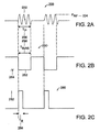
図2A−2Cは本発明によるコンフォーマルプラズマドーピングを実行するためのプラズマの発生及び外部源(即ちプラズマ以外の源)からのニュートラルの発生を示すタイミング図を示す。本発明の一実施例においては、プラズマ源101はコンフォーマルプラズマドーピング中パルス動作モードで動作する。図2Aは本発明によるプラズマドーピングに好適なパルスRF波形200を示す。パルスRF波形200はRFパルス202が開始するまで接地電位にある。RFパルス202はプラズマドーピングに適するように選択された電力レベルPRF204を有する。RFパルス202はパルス期間TP206後に終了し、接地電位に戻る。パルスRF波形200は、所望のプラズマプロセスパラメータとニュートラルを生成するために使用される吸着された膜層146’の再吸着レートとにより決まるデューティサイクルで周期的に繰り返す。
2A-2C show timing diagrams illustrating the generation of plasma and the generation of neutral from an external source (ie, a source other than plasma) to perform conformal plasma doping according to the present invention. In one embodiment of the present invention, the
図2Bは、バイアス電圧源148により発生されるバイアス電圧波形250を示す。バイアス電圧源148はプラズマドーピングを実行するためにバイアス期間TBias256中基板146に負電圧254を有する負電圧パルス252を供給する。負電圧254はプラズマ中のイオンを基板146へ引き付ける。バイアス期間TBias256は、プラズマがバイアス期間TBias256中のみ励起されるようにパルスRF波形200のパルス期間TP206に同期される。バイアス電圧波形250は、所望のプラズマプロセスパラメータとニュートラルを生成するために使用される吸着された膜層146’の再吸着速度とにより決まるデューティサイクルで周期的に繰り返す。
FIG. 2B shows a
種々の実施例においては、バイアス電圧波形250の周波数とデューティサイクルは、基板146又は構造部154上への膜層146’の再吸着が発生するのに十分な時間があるように選択される。例えば、一実施例においては、バイアス電圧波形250のパルス周波数とデューティサイクルは、個々のパルス間で十分な再吸着が発生するように選択される。他の実施例においては、バイアス電圧波形250は、所定数のパルスを有するパルス列の間に基板146又は構造部154上への膜層146’の再吸着が発生するのに十分な所定の時間を有する遅延を含むものとする。例えば、一実施例においては、コンフォーマルプラズマドーピングのために十分なニュートラルを発生させるために、100−1000パルスを有するパルス列の間にミリ秒領域の遅延時間を含むバイアス電圧波形250を用いる。
In various embodiments, the frequency and duty cycle of the
図2Cは、本発明において吸着された膜層146’を脱着させる放射源152の強度I282の波形280を示す。図2Cに示される実施例においては、放射源152の強度I282はRFパルス202の開始時に急速にパルスオンされる。種々の他の実施例においては、放射源152の強度I282は徐々に開始するものとし得ることを理解すべきである。また、図2Cに示される実施例においては、放射期間TR284はパルス期間TP206及びバイアス期間TBias256の一部分である。また、種々の実施例においては、放射期間TR284はパルス期間TP206及び/又はバイアス期間TBias256と同じ長さ又はパルス期間TP206及びバイアス期間TBias256より長くし得ることも理解すべきである。放射期間TR284の所望の長さは膜層146’の再吸着速度及び放射強度I282に関連する。
FIG. 2C shows a
放射源152は、プラズマ中のイオンを基板146へ引き付ける負電圧パルス252で基板146をバイアスするバイアス電圧源148と同期させることができる。例えば、放射源152は、コンフォーマルプラズマドーピングのために、イオンを基板146に引き付ける負電圧252の直前又は負電圧パルス252と同時に放射源がバースト放射を発生するようにバイアス電圧源148と同期させることができる。パルスRF波形200のデューティサイクルは、吸着された膜層146’が負電圧パルス252間で十分に脱着されるように選択する。
The
当業者は、コンフォーマルドーピングに関する本発明は従来のビームイオン注入システムとともに使用することもできることが理解されよう。ビームラインイオン注入システムは周知である。これらのシステムのターゲット又は基板はここに記載する膜を吸着するために使用することができる。代案として、図1と関連して記載する構造部154のような構造部を本発明による膜を吸着するために使用することもできる。次に、ここに記載するように放射源を使用して吸着された膜を脱着させてニュートラルを発生させることができる。ニュートラルはイオンビームからのイオンを散乱させ、これにより、よりコンフォーマルなイオン注入プロファイルが得られる。
One skilled in the art will appreciate that the present invention for conformal doping can also be used with conventional beam ion implantation systems. Beamline ion implantation systems are well known. The targets or substrates of these systems can be used to adsorb the films described herein. Alternatively, structures such as
等価例
本発明の教えを種々の実施例及び用例と関連して記載したが、本発明の教えはこれらの実施例に限定されるものではない。それどころか、本発明の教えは、当業者によく理解されるように、本発明の精神及び範囲から離れることなく成し得る種々の代替例、変更例及び等価例も含むものである。
Equivalent Examples While the teachings of the present invention have been described in connection with various embodiments and examples, the teachings of the present invention are not limited to these embodiments. On the contrary, the teachings of the present invention also include various alternatives, modifications and equivalents that may be made without departing from the spirit and scope of the present invention, as will be appreciated by those skilled in the art.
Claims (27)
b.プラズマドーピングのために基板を前記プラズマの近くに支持するプラテンと、
c.脱着されるとき複数のニュートラルを発生する膜を吸着した構造部と、
d.前記プラテンに電気的に接続された出力端子を有し、プラズマドーピングのために前記プラズマ中のイオンを基板に吸引する負電位を有するバイアス電圧波形を発生するバイアス電圧源と、
e.前記構造部上に吸着された膜を照射して前記吸着された膜を脱着させて複数のニュートラルを発生させる放射源とを備え、
イオンが基板に吸引される間前記複数のニュートラルがプラズマからのイオンを散乱させることでコンフォーマルプラズマドーピングを実行する、
ことを特徴とするプラズマドーピング装置。 a. A plasma source for generating pulsed plasma;
b. A platen that supports the substrate in proximity to the plasma for plasma doping;
c. A structure that adsorbs a membrane that generates multiple neutrals when desorbed;
d. A bias voltage source having an output terminal electrically connected to the platen and generating a bias voltage waveform having a negative potential for attracting ions in the plasma to the substrate for plasma doping;
e. A radiation source that irradiates the adsorbed film on the structure and desorbs the adsorbed film to generate a plurality of neutrals;
The plurality of neutrals scatter ions from the plasma while ions are attracted to the substrate to perform conformal plasma doping;
A plasma doping apparatus.
b.前記プラテンの近くに位置する構造部に膜を吸着させるステップと、
c.前記プラテンの近くにプラズマを発生させるステップと、
d.前記構造部上に吸着された膜を脱着させ、それによって複数のニュートラルを発生させるステップと、
e.前記プラテンを、プラズマドーピングのために前記プラズマ中のイオンを基板に吸引する負電位を有するバイアス電圧波形でバイアスするステップとを具え、
イオンが基板に吸引される間前記複数のニュートラルがプラズマからのイオンを散乱させることでコンフォーマルプラズマドーピングを実行する、
ことを特徴とするプラズマドーピング方法。 a. Positioning the substrate on the platen;
b. Adsorbing a film on a structure located near the platen;
c. Generating a plasma near the platen;
d. Desorbing the membrane adsorbed on the structure, thereby generating a plurality of neutrals;
e. Biasing the platen with a bias voltage waveform having a negative potential for attracting ions in the plasma to the substrate for plasma doping;
The plurality of neutrals scatter ions from the plasma while ions are attracted to the substrate to perform conformal plasma doping;
A plasma doping method characterized by the above.
b.ドーパント種を含むイオンを発生させる手段と、
c.前記構造部上に吸着された前記膜を脱着させて複数のニュートラルを発生させる手段とを備え、
前記複数のニュートラルがドーパント種を含むイオンを散乱させることによってコンフォーマルなドーピングを実行する、
コンフォーマルドーピング装置。 a. Means for adsorbing the film on the structure located near the platen supporting the substrate;
b. Means for generating ions including dopant species;
c. Means for desorbing the film adsorbed on the structure to generate a plurality of neutrals,
The plurality of neutrals perform conformal doping by scattering ions including dopant species;
Conformal doping equipment.
Applications Claiming Priority (3)
| Application Number | Priority Date | Filing Date | Title |
|---|---|---|---|
| US11/774,587 US20090008577A1 (en) | 2007-07-07 | 2007-07-07 | Conformal Doping Using High Neutral Density Plasma Implant |
| US11/774,587 | 2007-07-07 | ||
| PCT/US2008/067587 WO2009009272A2 (en) | 2007-07-07 | 2008-06-20 | Conformal doping using high neutral plasma implant |
Publications (3)
| Publication Number | Publication Date |
|---|---|
| JP2010532919A JP2010532919A (en) | 2010-10-14 |
| JP2010532919A5 JP2010532919A5 (en) | 2011-07-28 |
| JP5280440B2 true JP5280440B2 (en) | 2013-09-04 |
Family
ID=40220719
Family Applications (1)
| Application Number | Title | Priority Date | Filing Date |
|---|---|---|---|
| JP2010514994A Expired - Fee Related JP5280440B2 (en) | 2007-07-07 | 2008-06-20 | Conformal doping using high neutral density plasma implantation |
Country Status (6)
| Country | Link |
|---|---|
| US (1) | US20090008577A1 (en) |
| JP (1) | JP5280440B2 (en) |
| KR (1) | KR20100038404A (en) |
| CN (1) | CN101765679B (en) |
| TW (1) | TWI428965B (en) |
| WO (1) | WO2009009272A2 (en) |
Families Citing this family (7)
| Publication number | Priority date | Publication date | Assignee | Title |
|---|---|---|---|---|
| US8436318B2 (en) * | 2010-04-05 | 2013-05-07 | Varian Semiconductor Equipment Associates, Inc. | Apparatus for controlling the temperature of an RF ion source window |
| KR101455117B1 (en) * | 2014-07-23 | 2014-10-27 | 이에스엠주식회사 | Apparatus and method for encapsulation process of flexible display substrate |
| US10032604B2 (en) * | 2015-09-25 | 2018-07-24 | Applied Materials, Inc. | Remote plasma and electron beam generation system for a plasma reactor |
| FR3045206B1 (en) * | 2015-12-10 | 2020-01-03 | Ion Beam Services | ORDERING METHOD FOR AN IMPLANT OPERATING IN PLASMA IMMERSION |
| US10541137B2 (en) * | 2018-06-01 | 2020-01-21 | Varian Semiconductor Equipment Associates, Inc. | Method and apparatus for non line-of-sight doping |
| US11189462B1 (en) * | 2020-07-21 | 2021-11-30 | Tokyo Electron Limited | Ion stratification using bias pulses of short duration |
| US20230420219A1 (en) * | 2022-06-27 | 2023-12-28 | Austin Lo | Plasma-Enhanced Chemical Vapor Deposition for Structurally-Complex Substrates |
Family Cites Families (27)
| Publication number | Priority date | Publication date | Assignee | Title |
|---|---|---|---|---|
| US4217374A (en) * | 1978-03-08 | 1980-08-12 | Energy Conversion Devices, Inc. | Amorphous semiconductors equivalent to crystalline semiconductors |
| EP0032788B2 (en) * | 1980-01-16 | 1989-12-06 | National Research Development Corporation | Method for depositing coatings in a glow discharge |
| JPH0770512B2 (en) * | 1985-02-04 | 1995-07-31 | 日本電信電話株式会社 | Low energy ionized particle irradiation device |
| JPS61183925A (en) * | 1985-02-12 | 1986-08-16 | Nec Corp | Electron beam doping |
| JP2635021B2 (en) * | 1985-09-26 | 1997-07-30 | 宣夫 御子柴 | Deposition film forming method and apparatus used for the same |
| JPS6289861A (en) * | 1985-10-15 | 1987-04-24 | Showa Shinku:Kk | Method and apparatus for bombardment vapor deposition of thin film |
| JPH0618173B2 (en) * | 1986-06-19 | 1994-03-09 | 日本電気株式会社 | Thin film formation method |
| JP2590502B2 (en) * | 1987-12-10 | 1997-03-12 | 松下電器産業株式会社 | Impurity doping method |
| JP2588971B2 (en) * | 1989-07-06 | 1997-03-12 | 株式会社豊田中央研究所 | Laser deposition method and apparatus |
| EP0534505B1 (en) * | 1989-07-06 | 1998-12-09 | Toyota Jidosha Kabushiki Kaisha | Laser deposition method |
| JPH0448723A (en) * | 1990-06-15 | 1992-02-18 | Fuji Xerox Co Ltd | Manufacture of semiconductor device |
| JPH05217933A (en) * | 1992-02-06 | 1993-08-27 | Hitachi Ltd | Method of constructing surface structure |
| US6325078B2 (en) * | 1998-01-07 | 2001-12-04 | Qc Solutions, Inc., | Apparatus and method for rapid photo-thermal surface treatment |
| US6306265B1 (en) * | 1999-02-12 | 2001-10-23 | Applied Materials, Inc. | High-density plasma for ionized metal deposition capable of exciting a plasma wave |
| US6290825B1 (en) * | 1999-02-12 | 2001-09-18 | Applied Materials, Inc. | High-density plasma source for ionized metal deposition |
| US7223676B2 (en) * | 2002-06-05 | 2007-05-29 | Applied Materials, Inc. | Very low temperature CVD process with independently variable conformality, stress and composition of the CVD layer |
| US20030101935A1 (en) * | 2001-12-04 | 2003-06-05 | Walther Steven R. | Dose uniformity control for plasma doping systems |
| US20040016402A1 (en) * | 2002-07-26 | 2004-01-29 | Walther Steven R. | Methods and apparatus for monitoring plasma parameters in plasma doping systems |
| AU2003291176A1 (en) * | 2002-11-27 | 2004-06-23 | Ionwerks, Inc. | A time-of-flight mass spectrometer with improved data acquisition system |
| JP2005093518A (en) * | 2003-09-12 | 2005-04-07 | Matsushita Electric Ind Co Ltd | Control method and apparatus of dopant introduction |
| EP1676291B1 (en) * | 2003-10-20 | 2013-04-24 | Ionwerks, Inc. | Ion mobility tof/maldi/ms using drift cell alternating high and low electric field regions |
| US20050205211A1 (en) * | 2004-03-22 | 2005-09-22 | Vikram Singh | Plasma immersion ion implantion apparatus and method |
| US20060236931A1 (en) * | 2005-04-25 | 2006-10-26 | Varian Semiconductor Equipment Associates, Inc. | Tilted Plasma Doping |
| US7265368B2 (en) * | 2005-05-13 | 2007-09-04 | Applera Corporation | Ion optical mounting assemblies |
| US8642135B2 (en) * | 2005-09-01 | 2014-02-04 | Micron Technology, Inc. | Systems and methods for plasma doping microfeature workpieces |
| US20070084564A1 (en) * | 2005-10-13 | 2007-04-19 | Varian Semiconductor Equipment Associates, Inc. | Conformal doping apparatus and method |
| US7524743B2 (en) * | 2005-10-13 | 2009-04-28 | Varian Semiconductor Equipment Associates, Inc. | Conformal doping apparatus and method |
-
2007
- 2007-07-07 US US11/774,587 patent/US20090008577A1/en not_active Abandoned
-
2008
- 2008-06-20 JP JP2010514994A patent/JP5280440B2/en not_active Expired - Fee Related
- 2008-06-20 CN CN200880100529.3A patent/CN101765679B/en not_active Expired - Fee Related
- 2008-06-20 WO PCT/US2008/067587 patent/WO2009009272A2/en active Application Filing
- 2008-06-20 KR KR1020107002010A patent/KR20100038404A/en not_active Application Discontinuation
- 2008-06-24 TW TW097123555A patent/TWI428965B/en not_active IP Right Cessation
Also Published As
| Publication number | Publication date |
|---|---|
| CN101765679A (en) | 2010-06-30 |
| TWI428965B (en) | 2014-03-01 |
| JP2010532919A (en) | 2010-10-14 |
| KR20100038404A (en) | 2010-04-14 |
| TW200910428A (en) | 2009-03-01 |
| WO2009009272A3 (en) | 2009-03-05 |
| CN101765679B (en) | 2013-01-09 |
| US20090008577A1 (en) | 2009-01-08 |
| WO2009009272A2 (en) | 2009-01-15 |
Similar Documents
| Publication | Publication Date | Title |
|---|---|---|
| TWI443715B (en) | An apparatus for plasma processing a substrate and a method thereof | |
| US7524743B2 (en) | Conformal doping apparatus and method | |
| JP5280440B2 (en) | Conformal doping using high neutral density plasma implantation | |
| US9123509B2 (en) | Techniques for plasma processing a substrate | |
| KR100367662B1 (en) | Hyperthermal Neutral Particle Beam Source and Neutral Particle Beam Processing Apparatus Employing the Same | |
| US20070084564A1 (en) | Conformal doping apparatus and method | |
| US20060236931A1 (en) | Tilted Plasma Doping | |
| JP6366454B2 (en) | Method for processing an object | |
| US7820533B2 (en) | Multi-step plasma doping with improved dose control | |
| US20050205212A1 (en) | RF Plasma Source With Conductive Top Section | |
| JP2010532919A5 (en) | ||
| JP2010516062A (en) | Plasma source with liner for reducing metal contamination | |
| US20090104761A1 (en) | Plasma Doping System With Charge Control | |
| KR20230119044A (en) | Semiconductor processing system and method of implanting ions into a workpiece and processing a workpiece and etching a workpiece and depositing material on a workpiece | |
| US20090104719A1 (en) | Plasma Doping System with In-Situ Chamber Condition Monitoring | |
| KR19980086497A (en) | Sputtering device | |
| KR100476903B1 (en) | Neutral particle beam processing apparatus with enhanced conversion performance from plasma ions to neutral particles | |
| KR101010130B1 (en) | Electron beam curing equipment |
Legal Events
| Date | Code | Title | Description |
|---|---|---|---|
| A521 | Request for written amendment filed |
Free format text: JAPANESE INTERMEDIATE CODE: A523 Effective date: 20110608 |
|
| A621 | Written request for application examination |
Free format text: JAPANESE INTERMEDIATE CODE: A621 Effective date: 20110608 |
|
| A977 | Report on retrieval |
Free format text: JAPANESE INTERMEDIATE CODE: A971007 Effective date: 20130410 |
|
| TRDD | Decision of grant or rejection written | ||
| A01 | Written decision to grant a patent or to grant a registration (utility model) |
Free format text: JAPANESE INTERMEDIATE CODE: A01 Effective date: 20130507 |
|
| A61 | First payment of annual fees (during grant procedure) |
Free format text: JAPANESE INTERMEDIATE CODE: A61 Effective date: 20130522 |
|
| R150 | Certificate of patent or registration of utility model |
Free format text: JAPANESE INTERMEDIATE CODE: R150 |
|
| LAPS | Cancellation because of no payment of annual fees |