JP5268574B2 - Semiconductor integrated circuit device - Google Patents
Semiconductor integrated circuit device Download PDFInfo
- Publication number
- JP5268574B2 JP5268574B2 JP2008285858A JP2008285858A JP5268574B2 JP 5268574 B2 JP5268574 B2 JP 5268574B2 JP 2008285858 A JP2008285858 A JP 2008285858A JP 2008285858 A JP2008285858 A JP 2008285858A JP 5268574 B2 JP5268574 B2 JP 5268574B2
- Authority
- JP
- Japan
- Prior art keywords
- circuit
- transistor
- input
- source
- transistors
- Prior art date
- Legal status (The legal status is an assumption and is not a legal conclusion. Google has not performed a legal analysis and makes no representation as to the accuracy of the status listed.)
- Active
Links
Images


Classifications
-
- H—ELECTRICITY
- H03—ELECTRONIC CIRCUITRY
- H03F—AMPLIFIERS
- H03F3/00—Amplifiers with only discharge tubes or only semiconductor devices as amplifying elements
- H03F3/45—Differential amplifiers
- H03F3/45071—Differential amplifiers with semiconductor devices only
- H03F3/45076—Differential amplifiers with semiconductor devices only characterised by the way of implementation of the active amplifying circuit in the differential amplifier
- H03F3/45179—Differential amplifiers with semiconductor devices only characterised by the way of implementation of the active amplifying circuit in the differential amplifier using MOSFET transistors as the active amplifying circuit
- H03F3/45183—Long tailed pairs
-
- H—ELECTRICITY
- H03—ELECTRONIC CIRCUITRY
- H03F—AMPLIFIERS
- H03F1/00—Details of amplifiers with only discharge tubes, only semiconductor devices or only unspecified devices as amplifying elements
- H03F1/30—Modifications of amplifiers to reduce influence of variations of temperature or supply voltage or other physical parameters
-
- H—ELECTRICITY
- H03—ELECTRONIC CIRCUITRY
- H03F—AMPLIFIERS
- H03F3/00—Amplifiers with only discharge tubes or only semiconductor devices as amplifying elements
- H03F3/45—Differential amplifiers
- H03F3/45071—Differential amplifiers with semiconductor devices only
- H03F3/45479—Differential amplifiers with semiconductor devices only characterised by the way of common mode signal rejection
- H03F3/45632—Differential amplifiers with semiconductor devices only characterised by the way of common mode signal rejection in differential amplifiers with FET transistors as the active amplifying circuit
-
- H—ELECTRICITY
- H03—ELECTRONIC CIRCUITRY
- H03F—AMPLIFIERS
- H03F2200/00—Indexing scheme relating to amplifiers
- H03F2200/453—Controlling being realised by adding a replica circuit or by using one among multiple identical circuits as a replica circuit
-
- H—ELECTRICITY
- H03—ELECTRONIC CIRCUITRY
- H03F—AMPLIFIERS
- H03F2203/00—Indexing scheme relating to amplifiers with only discharge tubes or only semiconductor devices as amplifying elements covered by H03F3/00
- H03F2203/45—Indexing scheme relating to differential amplifiers
- H03F2203/45244—Indexing scheme relating to differential amplifiers the differential amplifier contains one or more explicit bias circuits, e.g. to bias the tail current sources, to bias the load transistors
-
- H—ELECTRICITY
- H03—ELECTRONIC CIRCUITRY
- H03F—AMPLIFIERS
- H03F2203/00—Indexing scheme relating to amplifiers with only discharge tubes or only semiconductor devices as amplifying elements covered by H03F3/00
- H03F2203/45—Indexing scheme relating to differential amplifiers
- H03F2203/45508—Indexing scheme relating to differential amplifiers the CSC comprising a voltage generating circuit as bias circuit for the CSC
Landscapes
- Engineering & Computer Science (AREA)
- Power Engineering (AREA)
- Amplifiers (AREA)
Abstract
Description
本発明は、所望のトランジスタ特性を確保し、かつAB級バイアスを実現できる半導体集積回路装置に関するものである。 The present invention relates to a semiconductor integrated circuit device capable of ensuring desired transistor characteristics and realizing a class AB bias.
高い線形性が要求されるような増幅器ではAB級のバイアス方法が採用される場合がある。入力信号が高周波数(例えば2.4GHz)の場合には例えば以下のようにしてそのAB級バイアスを実現可能である。容量結合を介した交流(以下、AC)信号と抵抗を介した直流(以下、DC)バイアス信号とを重畳して、ソースがGNDなどの基準電位に接地されたトランジスタのゲートに入力する。ここで、増幅器(トランジスタ)の特性については、例えば相互コンダクタンスgm一定の電流源を用いてDCバイアスを生成することで所望の特性を得ることができる。このような構成とすることで、ゲートに入力するAC信号の入力振幅が大きくなればトランジスタのDC出力電流も増加し、増幅器をAB級バイアスすることが可能になる(例えば、非特許文献1参照)。 An amplifier that requires high linearity may employ a class AB bias method. When the input signal has a high frequency (for example, 2.4 GHz), the class AB bias can be realized as follows, for example. An alternating current (hereinafter referred to as AC) signal via capacitive coupling and a direct current (hereinafter referred to as DC) bias signal via a resistor are superimposed and input to the gate of a transistor whose source is grounded to a reference potential such as GND. Here, as for the characteristics of the amplifier (transistor), for example, a desired characteristic can be obtained by generating a DC bias using a current source having a constant mutual conductance gm. With such a configuration, if the input amplitude of the AC signal input to the gate increases, the DC output current of the transistor also increases, and the amplifier can be biased to class AB (for example, see Non-Patent Document 1). ).
しかしながら、同様の構成で、入力信号が低周波数(例えば5MHz)の場合にはAC信号をコンデンサで容量結合しようとすると大きな容量が必要となり回路規模が増大する問題がある。そこで、容量結合を無くして、増幅器のAB級バイアスを実現するために、前段回路の出力信号(=前段出力コモンモードDC電圧+前段AC出力信号)を直接トランジスタのゲートに入力すると、トランジスタの特性(gmなど)が前段回路のコモンモード電圧で決まってしまい、所望の特性(gmなど)を得ることが難しい。ここで、トランジスタを所望の特性にする方法としては、前段にレベルシフタを挿入して所望のDCレベル(VDC)を得ることが考えられる。しかし、余分な回路が挿入されることによってどうしても歪みや雑音特性が劣化してしまうという問題が新たに発生する。その他の方法として、所望の特性を得るためにトランジスタのソースに流れる電流を定電流源で規制してしまうとA級バイアスになってしまい線形性が劣化してしまう。
そこで、本発明は上記の問題に鑑み、ある値にゲートDCバイアスされた増幅回路などのトランジスタに対して、所望のトランジスタ特性(gmなど)を確保し、かつ、AB級のバイアスを実現することができる半導体集積回路装置を提供することを目的とするものである。 In view of the above problems, the present invention secures desired transistor characteristics (gm, etc.) and realizes a class AB bias for a transistor such as an amplifier circuit that is gate DC biased to a certain value. An object of the present invention is to provide a semiconductor integrated circuit device capable of achieving the above.
本発明の一態様によれば、入力端子及び出力端子をそれぞれ1つ以上有する増幅回路と、前記増幅回路と直流的に同等な特性を有するレプリカ回路と、前記レプリカ回路のバイアス端子と基準電位点との間に設けられ、当該バイアス端子に参照電圧を生成する参照電圧生成回路と、前記レプリカ回路のバイアス端子に生成した前記参照電圧と前記増幅回路のバイアス端子に生成される電圧とが入力され、これら2つの電圧の差分を出力する差分回路と、前記増幅回路のバイアス端子と前記基準電位点との間に接続されるトランジスタとを有するフィードバック回路とを具備し、前記フィードバック回路は、前記差分を前記トランジスタのゲートに入力することによって、前記差分を前記増幅回路のバイアス端子にフィードバックし、前記増幅回路のバイアス端子に生成される電圧を前記レプリカ回路のバイアス端子に生成した前記参照電圧に等しくするようにフィードバック制御することを特徴とする半導体集積回路装置が提供される。
なお、参照電圧生成回路は、電流源で構成されることが好ましい。
According to one aspect of the present invention, an amplifier circuit having one or more input terminals and output terminals, a replica circuit having a DC equivalent characteristic to the amplifier circuit, a bias terminal of the replica circuit, and a reference potential point The reference voltage generation circuit for generating a reference voltage at the bias terminal, the reference voltage generated at the bias terminal of the replica circuit and the voltage generated at the bias terminal of the amplifier circuit are input. A feedback circuit having a difference circuit that outputs a difference between the two voltages and a transistor connected between a bias terminal of the amplifier circuit and the reference potential point, and the feedback circuit includes the difference circuit Is fed to the gate of the transistor, the difference is fed back to the bias terminal of the amplifier circuit, and the amplification is performed. The semiconductor integrated circuit device characterized by a feedback control so as to equalize the voltage generated in the bias terminal of the road to the reference voltage generated in the bias terminal of the replica circuit is provided.
The reference voltage generation circuit is preferably composed of a current source.
本発明の他の態様によれば、同じレベルの直流信号に互いに反転した交流信号が重畳された第1,第2の入力信号が入力される第1,第2の入力端子と、各ゲートに前記第1,第2の入力信号が入力され、各ソースが共通に接続されて差動対をなす第1,第2のトランジスタと、各一端部が前記第1,第2のトランジスタの各ドレインに接続され、各他端部が直流電圧源に接続された第1,第2の負荷と、前記第1,第2のトランジスタの各ドレインに接続され、出力信号を取り出す第1,第2の出力端子とを備えた増幅回路と、ゲートに前記第1,第2のトランジスタに入力される入力信号の直流成分と同じレベルの直流信号が入力される第3のトランジスタと、一端部が前記第3のトランジスタのドレインに接続され、他端部が前記直流電圧源に接続された第3の負荷とを備え、前記第3のトランジスタは前記増幅回路の前記第1,第2のトランジスタと直流的に同等な特性を有するレプリカ回路と、前記レプリカ回路の前記第3のトランジスタのソースと基準電位点との間に設けられた電流源で構成され、前記第3のトランジスタのソースと前記電流源の接続点に前記電流源に応じた参照電圧を生成する参照電圧生成回路と、前記増幅回路の前記第1,第2のトランジスタの共通接続されたソースと前記基準電位点との間にドレイン・ソースがそれぞれ接続され、該ドレイン・ソース間に流れる電流をゲートに入力する電圧にて制御する第4のトランジスタと、前記レプリカ回路の前記第3のトランジスタのソースに生成した前記参照電圧と前記増幅回路の前記第1,第2のトランジスタの共通接続されたソースに生成される電圧との差分をとる差分回路とを備え、該差分を前記第4のトランジスタのゲートに入力することによって、前記第1,第2のトランジスタの共通接続されたソースの電圧を前記レプリカ回路の前記第3のトランジスタのソースに生成した前記参照電圧に等しくするように負フィードバック制御するフィードバック回路と、を具備したことを特徴とする半導体集積回路装置が提供される。
なお、第4のトランジスタの相互コンダクタンス(gm)を可変する回路をさらに具備してもよい。
According to another aspect of the present invention, the first and second input terminals to which the first and second input signals in which the inverted AC signals are superimposed on the DC signal of the same level are input, and the gates are provided. The first and second input signals are input, the sources are connected in common to form a differential pair, and the first and second transistors form a differential pair, and each one end is the drain of each of the first and second transistors. Are connected to the first and second loads connected to the DC voltage source and the drains of the first and second transistors to extract the output signal. An amplifier circuit having an output terminal; a third transistor having a gate that receives a DC signal having the same level as the DC component of the input signal input to the first and second transistors; 3 is connected to the drain of the transistor No. 3, and the other end is the direct current A third load connected to a pressure source, wherein the third transistor has a direct current equivalent characteristic to the first and second transistors of the amplifier circuit, and the replica circuit A reference comprising a current source provided between the source of the third transistor and a reference potential point, and generating a reference voltage corresponding to the current source at a connection point of the source of the third transistor and the current source A drain and a source are connected between the voltage generating circuit and the commonly connected source of the first and second transistors of the amplifier circuit and the reference potential point, and a current flowing between the drain and the source is gated. A fourth transistor controlled by a voltage input to the reference circuit, the reference voltage generated at the source of the third transistor of the replica circuit, and the first and second of the amplifier circuit A differential circuit for taking a difference from a voltage generated at a commonly connected source of the transistor, and inputting the difference to a gate of the fourth transistor, thereby connecting the first and second transistors in common. And a feedback circuit that performs negative feedback control so that the source voltage is made equal to the reference voltage generated at the source of the third transistor of the replica circuit. Is done.
Note that a circuit for changing the mutual conductance (gm) of the fourth transistor may be further included.
本発明によれば、ある値にゲートDCバイアスされた増幅回路などのトランジスタに対して、所望のトランジスタ特性(gmなど)を確保し、かつ、AB級のバイアスを実現することができる半導体集積回路装置を提供することができる。 According to the present invention, a semiconductor integrated circuit capable of ensuring desired transistor characteristics (gm, etc.) and realizing class AB bias for a transistor such as an amplifier circuit whose gate is DC biased to a certain value. An apparatus can be provided.
発明の実施の形態を説明する前に、背景となる関連技術について図14〜図18を参照して説明する。
まず、AB級バイアスについて図14及び図15を参照して説明する。図14は、差動トランジスタM1,M2と、各差動トランジスタのドレインに直列接続した負荷抵抗R1,R2と、直流電圧源E(電源ラインで示している)とで構成される増幅回路装置を示している。ここでは、差動トランジスタM1,M2はNチャンネルFET(例えばNMOSトランジスタ)であるとしている。差動トランジスタM1,M2の各ゲートには、DCバイアスVDCに互いに極性反転したAC信号(以下、vp,vn信号)を加えた信号(VDC+vp,VDC+vn)を入力している。
Prior to the description of the embodiments of the present invention, related background technology will be described with reference to FIGS.
First, the class AB bias will be described with reference to FIGS. FIG. 14 shows an amplifier circuit device comprising differential transistors M1, M2, load resistors R1, R2 connected in series to the drains of the differential transistors, and a DC voltage source E (shown by a power supply line). Show. Here, the differential transistors M1 and M2 are assumed to be N-channel FETs (for example, NMOS transistors). Signals (VDC + vp, VDC + vn) obtained by adding AC signals (hereinafter, vp, vn signals) whose polarities are inverted to each other are input to the gates of the differential transistors M1, M2.
図15は図14の動作説明図であり、横軸にゲートに入力するAC入力振幅をとり、縦軸に差動トランジスタM1, M2のDC出力電流をとってある。AC成分が0のときには、DCバイアスVDCに基づいてDC電流IDCが差動トランジスタM1,M2の各ドレイン電流として流れ、AC成分の入力振幅が増大するのに伴ってそのDC出力電流が増加している。このように、DC出力電流が、DCバイアスVDCに基づいた初期値IDCから開始して、AC入力振幅の増大に伴って増加していく入出力状態をAB級増幅又はAB級バイアスと呼んでいる。一方、A級バイアスは常に一定のDC電流を出力しようとする構成であり、AC入力振幅が大きくなった場合には電流が足りずに増幅器の線形性が劣化してしまう。従って、高い線形性が要求されるような増幅器ではAB級のバイアス方法が採用される場合がある。 FIG. 15 is a diagram for explaining the operation of FIG. 14. The horizontal axis indicates the AC input amplitude input to the gate, and the vertical axis indicates the DC output current of the differential transistors M1 and M2. When the AC component is 0, a DC current IDC flows as each drain current of the differential transistors M1 and M2 based on the DC bias VDC, and the DC output current increases as the input amplitude of the AC component increases. Yes. Thus, the input / output state where the DC output current starts from the initial value IDC based on the DC bias VDC and increases as the AC input amplitude increases is called class AB amplification or class AB bias. . On the other hand, the class A bias is configured to always output a constant DC current, and when the AC input amplitude becomes large, the current is insufficient and the linearity of the amplifier deteriorates. Therefore, an amplifier that requires high linearity may employ a class AB bias method.
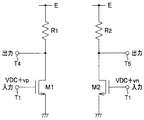
例えば、入力AC信号が高周波数(例えば2.4GHz)の場合には図16に示すようなAB級バイアスされた増幅回路装置が用いられる。図16に示す回路は、直流電圧源Eと電流源IとFETトランジスタM3と抵抗R3,R4とを有したDCバイアス生成回路と、AC信号入力端子T1a,T2aと、差動トランジスタM1,M2と、この差動トランジスタM1,M2の各ゲートにAC信号の交流成分vp,vnのみを入力するためのコンデンサC1,C2と、を備えた構成となっている。 For example, when the input AC signal has a high frequency (for example, 2.4 GHz), a class AB biased amplifier circuit device as shown in FIG. 16 is used. The circuit shown in FIG. 16 includes a DC bias generation circuit having a DC voltage source E, a current source I, an FET transistor M3, and resistors R3 and R4, AC signal input terminals T1a and T2a, and differential transistors M1 and M2. The differential transistors M1 and M2 have capacitors C1 and C2 for inputting only AC components vp and vn to the respective gates.
図16で、入力信号が高周波数の場合にはAC信号vp,vnをコンデンサC1,C2でAC成分のみとし、これらをDCバイアスVDCに重畳して差動トランジスタM1,M2の各ゲートに入力する。トランジスタM1,M2の特性(gmなど)は電流源(例えばgm一定電流源)Iで決まっている。vp,vnは入力AC信号であり、VDCはトランジスタM1,M2のゲートDCバイアスである。このDCバイアスVDCはgm一定の電流源Iの電流値を変えることによって電流値に応じた所望な値に設定できる。 In FIG. 16, when the input signal has a high frequency, the AC signals vp and vn are made only AC components by the capacitors C1 and C2, and these are superimposed on the DC bias VDC and input to the gates of the differential transistors M1 and M2. . The characteristics (gm, etc.) of the transistors M1, M2 are determined by a current source (for example, gm constant current source) I. vp and vn are input AC signals, and VDC is the gate DC bias of the transistors M1 and M2. The DC bias VDC can be set to a desired value according to the current value by changing the current value of the current source I having a constant gm.
しかし、入力信号が低周波数(例えば5MHz)の場合には図16のような増幅回路装置を用いることは難しい。何故なら、入力AC信号が低周波数信号の場合に図16のようなコンデンサC1,C2で容量結合しようとすると非常に大きなコンデンサが必要となりチップ面積を圧迫するためである。そこで、入力AC信号が低周波数の場合でも図17のような構成にすればAB級バイアスが可能である。M1,M2のゲートにはDCバイアスとしてVDCが、入力AC信号としてvp,vnが入力される。つまり、M1のゲートにはVDC+vpが入力され、M2のゲートにはVDC+vnが入力される。この場合、トランジスタM1,M2のゲートDCバイアス(VDC)は例えば前段回路の出力コモンモード電圧である。このため、トランジスタM1,M2の特性(gmなど)は前段回路のコモンモード電圧で決まってしまい、しきい値、温度などのばらつきによってトランジスタM1,M2の特性は大きくばらついてしまうことになる。 However, when the input signal has a low frequency (for example, 5 MHz), it is difficult to use an amplifier circuit device as shown in FIG. This is because when the input AC signal is a low-frequency signal, an attempt to capacitively couple the capacitors C1 and C2 as shown in FIG. 16 requires a very large capacitor, which reduces the chip area. Therefore, even when the input AC signal has a low frequency, class AB bias is possible if the configuration shown in FIG. 17 is used. The gates of M1 and M2 are supplied with VDC as a DC bias and vp and vn as input AC signals. That is, VDC + vp is input to the gate of M1, and VDC + vn is input to the gate of M2. In this case, the gate DC bias (VDC) of the transistors M1 and M2 is, for example, the output common mode voltage of the previous circuit. For this reason, the characteristics (gm and the like) of the transistors M1 and M2 are determined by the common mode voltage of the previous circuit, and the characteristics of the transistors M1 and M2 greatly vary due to variations in threshold value, temperature, and the like.
ここで、図17の差動トランジスタM1,M2を所望の特性にする方法としては、前段にレベルシフタを挿入して所望のDCレベル(VDC)を得ることが考えられる。しかし、余分な回路が挿入されることによってどうしても歪みや雑音特性が劣化してしまうという問題が新たに発生する。その他の方法として、所望の特性を得るために差動トランジスタM1,M2のソースに流れる電流を定電流源で規制してしまうとAC信号の入力振幅の増加に対しても出力電流が増えずほぼ一定値に制限され、A級バイアスになってしまい線形性が劣化してしまう。このようなケースは、例えば図18に示す無線送信機では、ミキサ回路13の入力段のトランジスタ回路で起こり得る。
Here, as a method of making the differential transistors M1 and M2 of FIG. 17 have desired characteristics, it is conceivable to obtain a desired DC level (VDC) by inserting a level shifter in the previous stage. However, there is a new problem that distortion and noise characteristics inevitably deteriorate due to insertion of an extra circuit. As another method, if the current flowing through the sources of the differential transistors M1 and M2 is regulated by a constant current source in order to obtain desired characteristics, the output current does not increase even when the input amplitude of the AC signal increases. It is limited to a constant value, resulting in a class A bias, and the linearity deteriorates. Such a case can occur, for example, in the transistor circuit at the input stage of the
図18は図16及び図17の回路装置が適用される無線送信機の構成例を示している。図18は後に述べる本発明の回路装置を適用させることもできる。無線送信機としては例えば携帯電話機や無線LANなどである。 FIG. 18 shows a configuration example of a wireless transmitter to which the circuit devices of FIGS. 16 and 17 are applied. The circuit device of the present invention described later can be applied to FIG. Examples of the wireless transmitter include a mobile phone and a wireless LAN.
図18において、無線送信機は、ベースバンドの入力信号が入力する入力端子11と、入力されたベースバンド信号の低域成分を通過させるローパスフィルタ(以下、LPF)12と、図示しないローカル発振器からの高周波数信号が入力される入力端子14と、この入力端子14に入力した高周波数信号とLPF12から出力された低周波数信号とを混合して高周波数の変調信号を生成するミキサ回路13と、ミキサ回路13からの変調信号を増幅して出力する出力アンプ15と、増幅された変調信号を図示しないアンテナに出力する出力端子16とを備えている。図18では、ベースバンド周波数(低周波数)で動作するローパスフィルタ(LPF)のコモンモード電圧がミキサ回路13の入力トランジスタ(図17の差動トランジスタM1,M2に相当)のゲートDCバイアスとなり、そこにLPF12からの低周波数AC信号が入力される。
In FIG. 18, a wireless transmitter includes an
そこで、本発明では、図17のミキサ回路13の入力段トランジスタ回路のようなケースにあるように、ある値にゲートDCバイアスされた増幅回路などのトランジスタ回路に対して、所望のトランジスタ特性(gmなど)を確保し、かつ、AB級のバイアスを実現する半導体集積回路装置を提供する。
Therefore, in the present invention, as in the case of the input stage transistor circuit of the
以下、発明の実施の形態について図1〜図13を参照して説明する。
図1は本発明に係る半導体集積回路装置のブロック図を示している。
図1において、半導体集積回路装置20は、入力端子T1及び出力端子T4を有する増幅回路21と、増幅回路21と直流的に同等な特性を有するレプリカ回路22と、レプリカ回路22のバイアス端子T7と基準電位点との間に設けられ、バイアス端子T7に参照電圧を生成する参照電圧生成回路23と、レプリカ回路22のバイアス端子T7に生成した参照電圧と増幅回路21のバイアス端子T6に生成される電圧との差分をとり、この差分を増幅回路21のバイアス端子T6に負フィードバックし、バイアス端子T6に生成される電圧をレプリカ回路22のバイアス端子T7に生成した参照電圧に等しくするようにフィードバック制御するフィードバック回路24とを備えている。
Hereinafter, embodiments of the present invention will be described with reference to FIGS.
FIG. 1 is a block diagram of a semiconductor integrated circuit device according to the present invention.
In FIG. 1, a semiconductor integrated
参照電圧生成回路23は、例えば電流源Iで構成されている。また、フィードバック回路24は、参照電圧生成回路23で生成した参照電圧VREFと増幅回路21のバイアス端子T6に生成される電圧との差分をとる差分回路としての差動アンプDIFと、この差分を増幅回路21のバイアス端子T6に負フィードバックするために、バイアス端子T6と基準電位点間に設けられたフィードバックの制御用のトランジスタM4とを備えている。
The reference
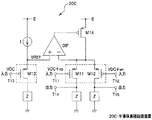
[第1の実施形態]
図2は本発明の第1の実施形態の半導体集積回路装置のブロック図を示している。
図2に示す半導体集積回路装置20Aにおいて、信号入力トランジスタとして差動対をなす差動トランジスタM1,M2があり、それらのソースは共通に接続され、その共通ソースがトランジスタM4のドレインに接続されている。トランジスタM3は、トランジスタM1,M2のレプリカである。差動トランジスタM1,M2のレプリカトランジスタM3のソースはある電流源Iと接続されている。トランジスタM3のソースと差動トランジスタM1,M2の共通ソースとはそれぞれ差動アンプDIFの2つの入力端に接続され、差動アンプDIFの出力端がトランジスタM4のゲートに接続される。つまり、トランジスタM3のソース電圧と差動トランジスタM1,M2のソース電圧は差動アンプDIFの±入力端に入力され、その差分出力がトランジスタM4のゲートに入力されている。トランジスタM4のソースは基準電位点に接続している。トランジスタM1,M2, M3のドレインはそれぞれ負荷Zを介して直流電圧源Eに接続されている。差動トランジスタM1,M2の各ゲートに接続した入力端子T1,T2にはDCバイアス(VDC)とAC信号(vp,vn)が入力され、トランジスタM3のゲートに接続した入力端子T3には差動トランジスタM1,M2と同様のゲートDCバイアス(VDC)が入力される。このトランジスタM3のゲートに入力されるVDCは例えば前段回路のコモンモード電圧である。なお、ここではトランジスタM1〜M4は全てNチャンネルFET(例えばNMOSトランジスタ)である。
[First Embodiment]
FIG. 2 is a block diagram of the semiconductor integrated circuit device according to the first embodiment of the present invention.
In the semiconductor integrated
次に、図2の作用効果を図3を参照しながら説明する。図3は図2の動作を説明する図である。
図3において、点線で囲んだ回路は、半導体集積回路装置20Aの本体トランジスタである差動トランジスタM1,M2のDC特性を確保するために設けられており、直流電圧源Eと基準電位点の間に、負荷Z,トランジスタM3,及び電流源Iが直列接続されている。トランジスタM3のゲートには図示しない前段回路の出力から取り出された直流成分が入力されているが、トランジスタM3の特性(gmなど)を決めているのは定電流源としての電流源Iであり、点線で囲んだ回路部分に流れる電流はこの電流源Iで決まる一定電流値に維持され、トランジスタM3のオーバードライブ電圧(=ゲート・ソース間電圧−トランジスタしきい値電圧)は一定値に維持されるように動作する。すなわち、トランジスタM3の特性(gm)は、トランジスタM3のゲートに入力される前段回路からの直流電圧VDCに依存せずに電流源Iの電流で決まる。つまり、点線で囲んだ回路部分から仮に電流源Iを削除して、トランジスタM3のソースを直接に基準電位点に接続する構成したとすると、トランジスタM3のオーバードライブ電圧は前段回路からの直流成分VDCに応じて変化する結果、トランジスタM3の特性(gm)も前段回路からの直流成分VDCで決まり、前段回路からの直流成分VDCでトランジスタM3の特性が変化してしまうことになる。本発明の実施形態では、トランジスタM3のバイアスが、ゲートに入力される前段回路からの直流成分VDCで決まるのではなくて、ソースに接続した電流源Iの電流で決められるように構成しているものである。なお、トランジスタM3のソースと電流源Iとの接続点に得られる参照電圧VREFは、電流源Iに対応した電圧値が得られるので、電流源Iの電流値を変えるか、或いは電流源I自体を代えれば参照電圧VREFを変えることができる。また、トランジスタM3のゲートに入力する直流電圧VDCを変化させても電流源Iが動作可能な範囲内で参照電圧VREFを変えることができる。すなわち、参照電圧VREFの値は、電流源Iの電流値によって変えられる一方、トランジスタM3のゲートに入力する直流電圧VDCの値によっても変えられる。しかしながら、ゲートに入力する直流電圧VDCは前段回路からの直流成分によって規定されるものであるから、ユーザーは参照電圧VREFの値を電流源Iの電流値を変えることによって所望の値に設定できることになる。
Next, the function and effect of FIG. 2 will be described with reference to FIG. FIG. 3 is a diagram for explaining the operation of FIG.
In FIG. 3, a circuit surrounded by a dotted line is provided to ensure the DC characteristics of the differential transistors M1 and M2, which are main transistors of the semiconductor integrated
さらに、本発明の実施形態では、差動アンプDIFによって差動トランジスタM1,M2のソース電位がトランジスタM3のソース電位(即ち参照電圧)VREFと等しくなるようにトランジスタM4を介してフィードバック制御が掛かるようになっている。つまり、差動トランジスタM1,M2の共通ソースの電位がトランジスタM3のソース電位VREFより例えば高くなった場合には、その正の差分値が差動アンプDIFからトランジスタM4りゲートに入力される結果、トランジスタM4を流れるドレイン電流が増加し、差動トランジスタM1,M2の各ドレイン電流も増加して共通ソースの電位が降下することにより参照電圧VREFに近づくように負フィードバックが掛かる。従って、差動アンプDIFによるフィードバックの帯域が信号帯域よりも広ければ、差動トランジスタM1,M2のソースは参照電位VREFに接地されていることになり、差動トランジスタM1,M2はAB級バイアスされている状態になる。また、トランジスタM3はある電流源I、例えばgm一定電流源でDCバイアスされており、VDC、しきい値、温度などのばらつきに寄らずトランジスタM3のgmは一定である。そして、差動トランジスタM1,M2のオーバードライブ電圧も差動アンプDIFによるフィードバックによりトランジスタM3のオーバードライブ電圧と等しくなる(これは、トランジスタM3は差動トランジスタM1,M2のレプリカであるためである)。そのため、差動トランジスタM1,M2のDCバイアス状態はトランジスタM3と等しく、gm一定でDCバイアスされていることになる。従って、図2の構成を用いるとAB級で差動トランジスタM1,M2をバイアスしながら、電流源Iによって所望の差動トランジスタM1,M2の特性(gm一定など)を得ることが可能となる。この構成の場合、図17の説明で述べたようなレベルシフタなど前段に余分な回路を挿入することによる歪みや雑音特性の劣化も生じない。ここで補足として、レプリカトランジスタM3は差動トランジスタM1,M2と全く同じである必要はないことを注記しておく。カレントミラーと同様に差動トランジスタM1,M2とトランジスタM3のサイズ比(チャンネル幅比など)でDCバイアス状態を調整可能である(そのサイズ比に合わせて負荷Zのサイズ比も変更する)。 Furthermore, in the embodiment of the present invention, the differential amplifier DIF performs feedback control via the transistor M4 so that the source potentials of the differential transistors M1 and M2 are equal to the source potential (ie, reference voltage) VREF of the transistor M3. It has become. That is, when the common source potential of the differential transistors M1 and M2 becomes higher than the source potential VREF of the transistor M3, for example, the positive difference value is input from the differential amplifier DIF to the gate of the transistor M4. The drain current flowing through the transistor M4 increases, the drain currents of the differential transistors M1 and M2 also increase, and the common source potential drops, so that negative feedback is applied so as to approach the reference voltage VREF. Therefore, if the feedback band by the differential amplifier DIF is wider than the signal band, the sources of the differential transistors M1 and M2 are grounded to the reference potential VREF, and the differential transistors M1 and M2 are class AB biased. It will be in the state. The transistor M3 is DC biased by a certain current source I, for example, a gm constant current source, and the gm of the transistor M3 is constant regardless of variations in VDC, threshold value, temperature, and the like. The overdrive voltages of the differential transistors M1 and M2 are also made equal to the overdrive voltage of the transistor M3 by feedback from the differential amplifier DIF (this is because the transistor M3 is a replica of the differential transistors M1 and M2). . Therefore, the DC bias state of the differential transistors M1 and M2 is equal to that of the transistor M3, and is DC biased at a constant gm. Therefore, when the configuration of FIG. 2 is used, it is possible to obtain desired characteristics of the differential transistors M1 and M2 (such as constant gm) by the current source I while biasing the differential transistors M1 and M2 in class AB. In the case of this configuration, distortion and noise characteristics are not deteriorated due to insertion of an extra circuit such as a level shifter as described in the explanation of FIG. Here, as a supplement, it should be noted that the replica transistor M3 does not have to be exactly the same as the differential transistors M1 and M2. Similar to the current mirror, the DC bias state can be adjusted by the size ratio (channel width ratio, etc.) of the differential transistors M1, M2 and the transistor M3 (the size ratio of the load Z is also changed in accordance with the size ratio).
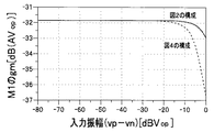
上記機能を確認するために回路シミュレーションを行った。図2の構成との比較のために、図4に示すような構成でのシミュレーション結果を合わせて示すことにする。図4は図2でA級にバイアスされた構成例を示している。
図4は、図2における差動アンプDIFは削除されており、直流電圧源Eと基準電位点間に、電流源Iと、ドレイン・ゲート間をダイオード接続したトランジスタM3とを直列接続し、トランジスタM3のゲートをトランジスタM4のゲートと共通に接続することによって、カレントミラーを構成している。それ以外の部分は図2と同様な構成である。
A circuit simulation was performed to confirm the above functions. For comparison with the configuration of FIG. 2, the simulation results of the configuration shown in FIG. 4 are also shown. FIG. 4 shows a configuration example biased to class A in FIG.
In FIG. 4, the differential amplifier DIF in FIG. 2 is omitted, and a current source I and a transistor M3 having a diode-connected drain and gate are connected in series between a DC voltage source E and a reference potential point. A current mirror is constructed by connecting the gate of M3 in common with the gate of the transistor M4. The other parts are the same as in FIG.
このような構成においては、図4の差動トランジスタM1,M2のDCバイアス状態(gmなど)は電流源Iをカレントミラーすることによって、図2の差動トランジスタM1,M2と同様になるようにしている。従って、差動トランジスタM1,M2を流れる電流、即ちトランジスタM4を流れる電流は電流源Iによって規定され、AC入力振幅(vp−vn)が増加してもトランジスタM4を流れるDC電流は殆ど増えないことになる。図2及び図4において、差動トランジスタM1,M2のDCバイアス状態(gm)は等しいが、図2はAB級、図4はA級でバイアスされていることになる。 In such a configuration, the DC bias state (gm, etc.) of the differential transistors M1 and M2 in FIG. 4 is made to be the same as that of the differential transistors M1 and M2 in FIG. 2 by current mirroring the current source I. ing. Accordingly, the current flowing through the differential transistors M1 and M2, that is, the current flowing through the transistor M4 is defined by the current source I, and the DC current flowing through the transistor M4 hardly increases even when the AC input amplitude (vp−vn) increases. become. 2 and 4, the DC bias states (gm) of the differential transistors M1 and M2 are equal, but FIG. 2 is biased by class AB and FIG. 4 is biased by class A.
図5はAC入力振幅(vp−vn)に対するトランジスタM4のDC電流の変化の様子を示している。
図5に示すように、図2の構成の場合、AC入力振幅の増加とともにトランジスタM4のDC電流も増加しており、AB級でバイアスされているのがわかる。一方、図4の構成の場合もAC入力振幅の増加とともにトランジスタM4のDC電流は若干増加しておりAB級動作しているようにも見えるが、実際にはA級動作となっており、これは図6を見れば明らかである。
FIG. 5 shows how the DC current of the transistor M4 changes with respect to the AC input amplitude (vp−vn).
As shown in FIG. 5, in the case of the configuration of FIG. 2, the DC current of the transistor M4 increases with the increase of the AC input amplitude, and it can be seen that it is biased with class AB. On the other hand, in the case of the configuration of FIG. 4, the DC current of the transistor M4 slightly increases with the increase of the AC input amplitude, and it appears that the class AB operation is performed. Is apparent from FIG.
図6はAC入力振幅(vp−vn)に対するトランジスタM4のドレイン電圧の変化の様子を示している。
図6に示すように、図4の構成の場合、AC入力振幅の増加に伴いトランジスタM4のドレイン電圧が増加している。従って、図4の構成でのトランジスタM4のDC電流の増加はトランジスタM4のチャネル長変調によって発生していることが分かる。つまり、図4の構成の場合、AC入力振幅の増加とともにトランジスタM4のドレイン電圧が増加するため、差動トランジスタM1,M2のトランジスタ特性(gmなど)は歪んでくると言える。一方、図2の構成では差動トランジスタM1,M2の歪み具合は図4の構成と比較して小さい。
FIG. 6 shows how the drain voltage of the transistor M4 changes with respect to the AC input amplitude (vp−vn).
As shown in FIG. 6, in the case of the configuration of FIG. 4, the drain voltage of the transistor M4 increases as the AC input amplitude increases. Therefore, it can be seen that the increase in the DC current of the transistor M4 in the configuration of FIG. 4 is caused by the channel length modulation of the transistor M4. In other words, in the configuration of FIG. 4, since the drain voltage of the transistor M4 increases as the AC input amplitude increases, it can be said that the transistor characteristics (gm, etc.) of the differential transistors M1 and M2 are distorted. On the other hand, in the configuration of FIG. 2, the degree of distortion of the differential transistors M1 and M2 is smaller than that of the configuration of FIG.
図7はAC入力振幅(vp−vn)に対するトランジスタM1 の相互コンダクタンスgmの変化の様子を示している。
図7に示すように、トランジスタM1のgmはAC入力振幅が小さい場合には図2,図4の構成ともに等しいことが分かる。つまり、図5から、図2の構成では差動トランジスタM1,M2をAB級でバイアスできており、図7から差動トランジスタM1,M2を所望のDCバイアス状態に設定可能(gm一定など)であることを示している。さらに前述のように、図2の構成の方が図4の構成の場合と比較して、AC入力振幅の増加によるgmの劣化具合が小さく歪みにくいこともわかる。
FIG. 7 shows how the mutual conductance gm of the transistor M1 changes with respect to the AC input amplitude (vp-vn).
As shown in FIG. 7, it can be seen that the gm of the transistor M1 is the same in both configurations of FIGS. 2 and 4 when the AC input amplitude is small. That is, from FIG. 5, the differential transistors M1 and M2 can be biased with class AB in the configuration of FIG. 2, and the differential transistors M1 and M2 can be set to a desired DC bias state (gm constant, etc.) from FIG. It shows that there is. Further, as described above, it can be seen that the configuration of FIG. 2 is less deteriorated due to the increase in the AC input amplitude and less distorted than the configuration of FIG.
図8はAC入力振幅に対するトランジスタM1のAC出力ドレイン電流を示している。
図8に示すように、信号電流は図2,図4ともにほぼ等しいが、3次, 5次歪み電流は図4と比較して図2の方が14dB程度小さいことがわかる。つまり、図7で示したのと同様に、図2の構成の方が図4の構成と比較して歪みにくいと言える。
FIG. 8 shows the AC output drain current of transistor M1 versus AC input amplitude.
As shown in FIG. 8, the signal currents are almost the same in FIGS. 2 and 4, but the third-order and fifth-order distortion currents are about 14 dB smaller in FIG. 2 than in FIG. That is, as shown in FIG. 7, it can be said that the configuration of FIG. 2 is less distorted than the configuration of FIG.
また、図2の構成は今後のCMOSプロセスの進展に伴う低電源電圧化に向いている。図4の構成と比較して図2の構成では、レプリカ回路、差動アンプで余分な電流を消費している。この余剰電流分だけ図4のDCバイアス電流を上げれば、図4でも確かに線形性を高くすることができる。しかし、電源電圧が低い場合にDCバイアス電流を上げていくと、差動トランジスタM1,M2のドレイン電圧が下がってきて差動トランジスタM1,M2が飽和領域で動作しなくなってしまう。一方、図2の構成の場合は、差動トランジスタM1,M2に流れるDCバイアス電流を直接上げるのではなく、その分の電流をレプリカ回路、差動アンプに流すことで線形性を上げる構成になっている。つまり、図4の構成の場合と比較して、差動トランジスタM1,M2の動作点を変更することなく線形性を上げることが可能であり、低電源電圧に向いた構成になっている。 Further, the configuration of FIG. 2 is suitable for lowering the power supply voltage with the progress of the CMOS process in the future. Compared to the configuration of FIG. 4, the configuration of FIG. 2 consumes extra current in the replica circuit and the differential amplifier. If the DC bias current of FIG. 4 is increased by this surplus current, the linearity can be certainly improved in FIG. However, if the DC bias current is increased when the power supply voltage is low, the drain voltages of the differential transistors M1 and M2 decrease, and the differential transistors M1 and M2 do not operate in the saturation region. On the other hand, the configuration shown in FIG. 2 does not directly increase the DC bias current flowing in the differential transistors M1 and M2, but increases the linearity by flowing the corresponding current through the replica circuit and the differential amplifier. ing. That is, as compared with the configuration of FIG. 4, the linearity can be improved without changing the operating points of the differential transistors M1 and M2, and the configuration is suitable for a low power supply voltage.
第1の実施形態によれば、レプリカトランジスタM3を利用して本体トランジスタM1,M2のソース電位を制御することによって、ある値にゲートDCバイアスされた増幅回路などのトランジスタに対して、所望のトランジスタ特性を確保し、かつ、AB級のバイアスを実現することができる。 According to the first embodiment, by using the replica transistor M3 to control the source potentials of the main body transistors M1 and M2, a desired transistor with respect to a transistor such as an amplifier circuit whose gate is DC biased to a certain value. The characteristics can be secured and the AB class bias can be realized.
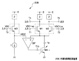
[第2の実施形態]
図9は本発明の第2の実施形態の半導体集積回路装置の回路図を示している。
図9に示す半導体集積回路装置20Bが、図2の半導体集積回路装置20Aと異なる点は、トランジスタM4のサイズ(チャンネル幅など)と等価な部分を調整することによってトランジスタM4の入力振幅の増加に伴うドレイン電流の増加量を調整可能にしたトランジスタ、即ちgm調整可能なトランジスタM4-1を設けたものである。これによって、図5の二点鎖線に示すようにトランジスタM4のDC電流を増加させたり減少させたりして、トランジスタM4のgmを可変することができる。
[Second Embodiment]
FIG. 9 shows a circuit diagram of a semiconductor integrated circuit device according to the second embodiment of the present invention.
The semiconductor integrated circuit device 20B shown in FIG. 9 is different from the semiconductor integrated
図10はgm調整可能なトランジスタM4-1の構成例を示している。トランジスタM4-1は、差動アンプDIFからの差分信号が入力されるフィードバック入力端子T10と、フィードバック出力端子T8と、図示しない制御手段からの制御信号が入力される制御端子T9と、フィードバック出力端子T8と基準電位点間に並列に接続した複数(例えば3つ)のトランジスタM4a,M4b,M4cと、フィードバック入力端子T10と3つのトランジスタM4a,M4b,M4cのゲート間に設けられて、フィードバック入力端子T10からの差分信号をトランジスタM4aのゲートのみに供給するか、トランジスタM4aのゲートともう1つのトランジスタM4bのゲートに供給するか、或いは、トランジスタM4aのゲートと他の2つのトランジスタM4b及びM4cのゲートに供給するかを、制御端子T9からの制御信号に応じて選択可能にするgm可変部31とを備えている。 FIG. 10 shows a configuration example of the transistor M4-1 capable of adjusting gm. The transistor M4-1 includes a feedback input terminal T10 to which a differential signal from the differential amplifier DIF is input, a feedback output terminal T8, a control terminal T9 to which a control signal from control means (not shown) is input, and a feedback output terminal A plurality of (for example, three) transistors M4a, M4b, and M4c connected in parallel between T8 and the reference potential point, and a feedback input terminal provided between the feedback input terminal T10 and the gates of the three transistors M4a, M4b, and M4c The differential signal from T10 is supplied only to the gate of transistor M4a, to the gate of transistor M4a and the gate of another transistor M4b, or the gate of transistor M4a and the gates of the other two transistors M4b and M4c Gm variable section that enables selection according to the control signal from the control terminal T9 It is equipped with a 1 and.
この構成においては、図示しない制御手段からの制御信号の内容に応じて、gm可変部31が3つのトランジスタM4a,M4b,M4cの3つのゲートのうちの幾つのゲートに差動アンプDIFからの差分信号を入力するかを選択することによって、トランジスタM4-1の特性パラメータであるgmを可変することが可能となる。
In this configuration, the gm
第2の実施形態によれば、フィードバック制御用のトランジスタM4-1を流れる電流を調整することにより、本体トランジスタM1,M2の信号電流増加に伴う出力電流増加度合いを調整できるので、本体トランジスタのgmを可変して、増幅回路の出力の歪み方を調整することが可能となる。 According to the second embodiment, by adjusting the current flowing through the feedback control transistor M4-1, the degree of increase in the output current accompanying the increase in the signal current of the main body transistors M1 and M2 can be adjusted. Can be adjusted to adjust the distortion of the output of the amplifier circuit.
[第3の実施形態]
図11は本発明の第3の実施形態の半導体集積回路装置のブロック図を示している。
図11に示す半導体集積回路装置20Cにおいて、信号入力トランジスタとして差動対をなす差動トランジスタM11,M12があり、それらのソースがトランジスタM14のドレインに接続されている。トランジスタM13は、トランジスタM11,M12のレプリカである。差動トランジスタM11,M12のレプリカトランジスタM13のソースはある電流源Iと接続されている。電流源Iの一端は直流電圧源Eに接続している。なお、トランジスタM11〜M14は全てPチャンネルFET(例えばPMOSトランジスタ)である。
[Third Embodiment]
FIG. 11 is a block diagram of a semiconductor integrated circuit device according to the third embodiment of the present invention.
In the semiconductor integrated circuit device 20C shown in FIG. 11, there are differential transistors M11 and M12 forming a differential pair as signal input transistors, and their sources are connected to the drain of the transistor M14. The transistor M13 is a replica of the transistors M11 and M12. The sources of the replica transistors M13 of the differential transistors M11 and M12 are connected to a certain current source I. One end of the current source I is connected to a DC voltage source E. The transistors M11 to M14 are all P-channel FETs (for example, PMOS transistors).
トランジスタM13のソースと差動トランジスタM11,M12のソースは差動アンプDIFの2つの入力端に接続され、その出力端がトランジスタM14のゲートに接続される。つまり、トランジスタM13のソース電圧と差動トランジスタM11,M12のソース電圧は差動アンプDIFの±入力端に入力され、その差分出力がトランジスタM14のゲートに入力される。トランジスタM14のソースは直流電圧源Eに接続している。トランジスタM11,M12, M13のドレインはそれぞれ負荷Zを介して基準電位点に接続されている。差動トランジスタM11,M12のゲートにはDCバイアス(VDC)とAC信号(vp,vn)が入力され、トランジスタM13のゲートには差動トランジスタM11,M12と同様のゲートDCバイアス(VDC)が入力される。このトランジスタM13に入力されるVDCは例えば前段回路のコモンモード電圧である。 The source of the transistor M13 and the sources of the differential transistors M11 and M12 are connected to the two input terminals of the differential amplifier DIF, and the output terminal is connected to the gate of the transistor M14. That is, the source voltage of the transistor M13 and the source voltages of the differential transistors M11 and M12 are input to the ± input terminal of the differential amplifier DIF, and the difference output is input to the gate of the transistor M14. The source of the transistor M14 is connected to the DC voltage source E. The drains of the transistors M11, M12, and M13 are connected to the reference potential point via the load Z, respectively. A DC bias (VDC) and an AC signal (vp, vn) are input to the gates of the differential transistors M11 and M12, and a gate DC bias (VDC) similar to that of the differential transistors M11 and M12 is input to the gate of the transistor M13. Is done. The VDC input to the transistor M13 is, for example, the common mode voltage of the previous circuit.
上記の図11の構成においては、図2の半導体集積回路装置20Aの構成における上下を逆にし、NチャンネルFETをPチャンネルFETに置き換えた構成としたものである。図11の半導体集積回路装置20Cの動作は図2と同様である。
In the configuration of FIG. 11 described above, the configuration of the semiconductor integrated
第3の実施形態によれば、PチャンネルFET例えばPMOSトランジスタを用いた半導体集積回路装置においても、第1の実施形態と同様に、レプリカトランジスタM13を利用して本体トランジスタM11,M12のソース電位を制御することによって、ある値にゲートDCバイアスされた増幅回路などのトランジスタに対して、所望のトランジスタ特性を確保し、かつ、AB級のバイアスを実現することができる。 According to the third embodiment, even in a semiconductor integrated circuit device using a P-channel FET, for example, a PMOS transistor, the source potentials of the body transistors M11 and M12 are set using the replica transistor M13 as in the first embodiment. By controlling, it is possible to secure desired transistor characteristics and realize AB class bias for a transistor such as an amplifier circuit whose gate is DC biased to a certain value.
[第4の実施形態]
図12は本発明の第4の実施形態の半導体集積回路装置のブロック図を示している。
図12に示す半導体集積回路装置20Dは、図2の半導体集積回路装置2AにおけるトランジスタM2及びその負荷Zを削除して、増幅回路をトランジスタM1とその負荷Zのみで構成したものである。ここで、トランジスタM3は、トランジスタM1のレプリカである。つまり、トランジスタM3はその直流特性がトランジスタM1と同等な直流特性を有するレプリカである。トランジスタM3のドレイン・ソース間を流れる直流電流は、トランジスタM1のドレイン・ソース間を流れる直流電流と同等である。その他の構成及び動作は、図2と同様である。
[Fourth Embodiment]
FIG. 12 is a block diagram of a semiconductor integrated circuit device according to the fourth embodiment of the present invention.
In the semiconductor integrated circuit device 20D shown in FIG. 12, the transistor M2 and its load Z in the semiconductor integrated circuit device 2A of FIG. 2 are deleted, and the amplifier circuit is configured by only the transistor M1 and its load Z. Here, the transistor M3 is a replica of the transistor M1. That is, the transistor M3 is a replica whose DC characteristic is equivalent to that of the transistor M1. The direct current flowing between the drain and source of the transistor M3 is equivalent to the direct current flowing between the drain and source of the transistor M1. Other configurations and operations are the same as those in FIG.
図13に示す半導体集積回路装置20Eは、図12の装置における上下を逆にし、NチャンネルFETをPチャンネルFETに置き換えた構成としたものである。
第4の実施形態によれば、差動トランジスタを用いた半導体集積回路装置に限らず、信号増幅用の本体トランジスタが1つの半導体集積回路装置においても、第1及び第3の実施形態と同様に、レプリカトランジスタM3又はM13を利用して本体トランジスタM1又はM11のソース電位を制御することによって、ある値にゲートDCバイアスされた増幅回路などのトランジスタに対して、所望のトランジスタ特性を確保し、かつ、AB級のバイアスを実現することができる。
A semiconductor integrated
According to the fourth embodiment, not only in a semiconductor integrated circuit device using a differential transistor, but also in a semiconductor integrated circuit device having one main transistor for signal amplification, as in the first and third embodiments. By using the replica transistor M3 or M13 to control the source potential of the body transistor M1 or M11, a desired transistor characteristic is ensured for a transistor such as an amplifier circuit whose gate is DC biased to a certain value, and A class AB bias can be realized.
20,20A,20B,20C,20D,20E…半導体集積回路装置
21…増幅回路
22…レプリカ回路
23…参照電圧生成回路
24…フィードバック回路
M1,M2,M3,M4…NチャンネルFET
M11,M12,M13,M14…PチャンネルFET
DIF…差動アンプ
E…直流電圧源
I…電流源FET
20, 20A, 20B, 20C, 20D, 20E ... Semiconductor integrated circuit device
21 ... Amplifier circuit
22 ...
M11, M12, M13, M14 ... P-channel FET
DIF ... differential amplifier E ... DC voltage source I ... current source FET
Claims (4)
前記増幅回路と直流的に同等な特性を有するレプリカ回路と、
前記レプリカ回路のバイアス端子と基準電位点との間に設けられ、当該バイアス端子に参照電圧を生成する参照電圧生成回路と、
前記レプリカ回路のバイアス端子に生成した前記参照電圧と前記増幅回路のバイアス端子に生成される電圧とが入力され、これら2つの電圧の差分を出力する差分回路と、前記増幅回路のバイアス端子と前記基準電位点との間に接続されるトランジスタとを有するフィードバック回路とを具備し、
前記フィードバック回路は、前記差分を前記トランジスタのゲートに入力することによって、前記差分を前記増幅回路のバイアス端子にフィードバックし、前記増幅回路のバイアス端子に生成される電圧を前記レプリカ回路のバイアス端子に生成した前記参照電圧に等しくするようにフィードバック制御する
ことを特徴とする半導体集積回路。 An amplifier circuit having at least one input terminal and one output terminal;
A replica circuit having direct current equivalent characteristics to the amplifier circuit;
A reference voltage generation circuit that is provided between the bias terminal of the replica circuit and a reference potential point and generates a reference voltage at the bias terminal;
The reference voltage generated at the bias terminal of the replica circuit and the voltage generated at the bias terminal of the amplifier circuit are input, a difference circuit that outputs a difference between these two voltages, a bias terminal of the amplifier circuit, A feedback circuit having a transistor connected to a reference potential point,
The feedback circuit feeds the difference to the bias terminal of the amplifier circuit by inputting the difference to the gate of the transistor, and the voltage generated at the bias terminal of the amplifier circuit is applied to the bias terminal of the replica circuit. A semiconductor integrated circuit characterized by performing feedback control so as to be equal to the generated reference voltage .
ゲートに前記第1,第2のトランジスタに入力される入力信号の直流成分と同じレベルの直流信号が入力される第3のトランジスタと、一端部が前記第3のトランジスタのドレインに接続され、他端部が前記直流電圧源に接続された第3の負荷とを備え、前記第3のトランジスタは前記増幅回路の前記第1,第2のトランジスタと直流的に同等な特性を有するレプリカ回路と、
前記レプリカ回路の前記第3のトランジスタのソースと基準電位点との間に設けられた電流源で構成され、前記第3のトランジスタのソースと前記電流源の接続点に前記電流源に応じた参照電圧を生成する参照電圧生成回路と、
前記増幅回路の前記第1,第2のトランジスタの共通接続されたソースと前記基準電位点との間にドレイン・ソースがそれぞれ接続され、該ドレイン・ソース間に流れる電流をゲートに入力する電圧にて制御する第4のトランジスタと、前記レプリカ回路の前記第3のトランジスタのソースに生成した前記参照電圧と前記増幅回路の前記第1,第2のトランジスタの共通接続されたソースに生成される電圧との差分をとる差分回路とを備え、該差分を前記第4のトランジスタのゲートに入力することによって、前記第1,第2のトランジスタの共通接続されたソースの電圧を前記レプリカ回路の前記第3のトランジスタのソースに生成した前記参照電圧に等しくするように負フィードバック制御するフィードバック回路と、
を具備したことを特徴とする半導体集積回路装置。 First and second input terminals to which first and second input signals in which AC signals inverted from each other are superimposed on DC signals of the same level are input, and the first and second input signals to each gate. The first and second transistors that are input and have their sources connected in common to form a differential pair, and each one end is connected to each drain of the first and second transistors, and each other end is a direct current An amplifying circuit comprising first and second loads connected to a voltage source, and first and second output terminals connected to the drains of the first and second transistors for extracting an output signal;
A third transistor in which a DC signal having the same level as the DC component of the input signal input to the first and second transistors is input to the gate; one end of which is connected to the drain of the third transistor; A third load having an end connected to the DC voltage source, and the third transistor having a DC equivalent characteristic to the first and second transistors of the amplifier circuit;
The current source provided between the source of the third transistor of the replica circuit and a reference potential point, and a reference point corresponding to the current source at the connection point of the source of the third transistor and the current source A reference voltage generation circuit for generating a voltage;
A drain and a source are respectively connected between the commonly connected source of the first and second transistors of the amplifier circuit and the reference potential point, and a current flowing between the drain and the source is converted to a voltage input to the gate. And the reference voltage generated at the source of the third transistor of the replica circuit and the voltage generated at the commonly connected source of the first and second transistors of the amplifier circuit. And a difference circuit that takes the difference between the first and second transistors by inputting the difference to the gate of the fourth transistor, thereby obtaining the voltage of the source connected in common to the first and second transistors. A feedback circuit that performs negative feedback control to equalize the reference voltage generated at the source of the three transistors;
A semiconductor integrated circuit device comprising:
Priority Applications (2)
| Application Number | Priority Date | Filing Date | Title |
|---|---|---|---|
| JP2008285858A JP5268574B2 (en) | 2008-11-06 | 2008-11-06 | Semiconductor integrated circuit device |
| US12/560,828 US7898332B2 (en) | 2008-11-06 | 2009-09-16 | Semiconductor integrated circuit device |
Applications Claiming Priority (1)
| Application Number | Priority Date | Filing Date | Title |
|---|---|---|---|
| JP2008285858A JP5268574B2 (en) | 2008-11-06 | 2008-11-06 | Semiconductor integrated circuit device |
Publications (2)
| Publication Number | Publication Date |
|---|---|
| JP2010114689A JP2010114689A (en) | 2010-05-20 |
| JP5268574B2 true JP5268574B2 (en) | 2013-08-21 |
Family
ID=42130657
Family Applications (1)
| Application Number | Title | Priority Date | Filing Date |
|---|---|---|---|
| JP2008285858A Active JP5268574B2 (en) | 2008-11-06 | 2008-11-06 | Semiconductor integrated circuit device |
Country Status (2)
| Country | Link |
|---|---|
| US (1) | US7898332B2 (en) |
| JP (1) | JP5268574B2 (en) |
Families Citing this family (17)
| Publication number | Priority date | Publication date | Assignee | Title |
|---|---|---|---|---|
| US9166533B2 (en) | 2009-07-30 | 2015-10-20 | Qualcomm Incorporated | Bias current monitor and control mechanism for amplifiers |
| US8284581B2 (en) * | 2009-12-07 | 2012-10-09 | Texas Instruments Incorporated | Active rectifier and method for energy harvesting power management circuit |
| US8665005B2 (en) * | 2010-12-03 | 2014-03-04 | Marvell World Trade Ltd. | Process and temperature insensitive inverter |
| US8786321B2 (en) * | 2010-12-30 | 2014-07-22 | Stmicroelectronics International N.V. | Power harvesting in open drain transmitters |
| US8410847B2 (en) * | 2011-05-09 | 2013-04-02 | Analog Devices, Inc. | Input common mode voltage compensation circuit |
| US8836374B2 (en) * | 2011-06-24 | 2014-09-16 | Broadcom Corporation | High performance pre-mixer buffer in wireless communications systems |
| US9154079B2 (en) | 2012-10-24 | 2015-10-06 | Qualcomm Incorporated | Threshold tracking bias voltage for mixers |
| US8761707B1 (en) * | 2013-03-11 | 2014-06-24 | Futurewei Technologies, Inc. | Radio frequency low noise amplifier load circuit |
| CN105684302A (en) | 2013-11-04 | 2016-06-15 | 马维尔国际贸易有限公司 | Memory effect reduction using low impedance biasing |
| CN104808729B (en) * | 2014-01-27 | 2017-10-13 | 澜起科技(上海)有限公司 | A kind of voltage-stablizer and the method for voltage stabilizing |
| US9467061B2 (en) * | 2014-08-29 | 2016-10-11 | Infineon Technologies Austria Ag | System and method for driving a transistor |
| US9559683B2 (en) | 2014-08-29 | 2017-01-31 | Infineon Technologies Austria Ag | System and method for a switch having a normally-on transistor and a normally-off transistor |
| US9479159B2 (en) | 2014-08-29 | 2016-10-25 | Infineon Technologies Austria Ag | System and method for a switch having a normally-on transistor and a normally-off transistor |
| WO2016051473A1 (en) | 2014-09-29 | 2016-04-07 | 三菱電機株式会社 | Operational amplifier circuit |
| GB2533309A (en) * | 2014-12-15 | 2016-06-22 | Nordic Semiconductor Asa | Differential amplifiers |
| US9793861B1 (en) | 2016-07-28 | 2017-10-17 | Qualcomm Incorporated | Amplification systems |
| FR3115426B1 (en) | 2020-08-31 | 2023-10-27 | St Microelectronics Grenoble 2 | Operational amplifier |
Family Cites Families (8)
| Publication number | Priority date | Publication date | Assignee | Title |
|---|---|---|---|---|
| FR2493069A1 (en) * | 1980-10-23 | 1982-04-30 | Efcis | INTEGRATED AMPLIFIER IN CLASS AB IN CMOS TECHNOLOGY |
| JPH05252020A (en) * | 1992-03-06 | 1993-09-28 | Fujitsu Ltd | Cmos drive circuit |
| JPH07106875A (en) * | 1993-09-30 | 1995-04-21 | Nec Corp | Semiconductor integrated circuit |
| JP2002076800A (en) * | 2000-08-30 | 2002-03-15 | Nec Corp | Voltage subtracter/adder and mos differential amplifier circuit to achieve the same |
| JP4099079B2 (en) * | 2003-02-12 | 2008-06-11 | 日本電信電話株式会社 | Bias generation circuit |
| EP1626496B1 (en) * | 2004-08-13 | 2008-10-08 | Dialog Semiconductor GmbH | Differential gain stage for low voltage supply |
| JP4920219B2 (en) * | 2005-08-30 | 2012-04-18 | 株式会社東芝 | Operational amplifier |
| US7525381B2 (en) * | 2007-03-09 | 2009-04-28 | Analog Devices, Inc. | Amplifier structures that enhance transient currents and signal swing |
-
2008
- 2008-11-06 JP JP2008285858A patent/JP5268574B2/en active Active
-
2009
- 2009-09-16 US US12/560,828 patent/US7898332B2/en active Active
Also Published As
| Publication number | Publication date |
|---|---|
| US20100109781A1 (en) | 2010-05-06 |
| US7898332B2 (en) | 2011-03-01 |
| JP2010114689A (en) | 2010-05-20 |
Similar Documents
| Publication | Publication Date | Title |
|---|---|---|
| JP5268574B2 (en) | Semiconductor integrated circuit device | |
| JP4991785B2 (en) | Semiconductor integrated circuit device | |
| US7868695B2 (en) | Differential amplifier | |
| KR100682056B1 (en) | Buffer Amplifier | |
| US7161406B1 (en) | Method and apparatus for providing non 2:1 Gilbert cell mixer | |
| US20060202760A1 (en) | Controllable amplifier and the use thereof | |
| JP5239451B2 (en) | Differential single phase converter circuit | |
| US9503053B1 (en) | Active balun for wideband applications | |
| CN107896095B (en) | Fully differential operational amplifier | |
| US8953346B2 (en) | Converting circuit for converting input voltage into output current | |
| US7948294B2 (en) | Mixer with high linearity | |
| US10348260B2 (en) | Amplifier circuit and filter | |
| US10707814B2 (en) | Amplifier device | |
| KR19980036295A (en) | Mixers with Replication Voltage-to-Current Converter | |
| US7378908B2 (en) | Variable gain differential amplifier, and variable degeneration impedance control device and method for use in the same | |
| KR19980070499A (en) | An electronic circuit including a differential circuit | |
| US7038501B2 (en) | Transconductor circuit for compensating the distortion of output current | |
| US11437963B2 (en) | Amplifiers for RF ADCS | |
| JP2008172791A (en) | Voltage controlled oscillator for controlling phase noise, and method using the same | |
| Likittanapong et al. | Linear CMOS triode transconductor for low-voltage applications | |
| JP4550805B2 (en) | Random sequence generator | |
| KR100618354B1 (en) | Ultra wide band filter for using cross-coupled transistor pair | |
| JP5139963B2 (en) | Differential amplifier | |
| JP5205403B2 (en) | Semiconductor integrated circuit device | |
| JP4867066B2 (en) | Amplifier circuit |
Legal Events
| Date | Code | Title | Description |
|---|---|---|---|
| A621 | Written request for application examination |
Free format text: JAPANESE INTERMEDIATE CODE: A621 Effective date: 20110323 |
|
| A977 | Report on retrieval |
Free format text: JAPANESE INTERMEDIATE CODE: A971007 Effective date: 20120112 |
|
| A131 | Notification of reasons for refusal |
Free format text: JAPANESE INTERMEDIATE CODE: A131 Effective date: 20120117 |
|
| A521 | Written amendment |
Free format text: JAPANESE INTERMEDIATE CODE: A523 Effective date: 20120307 |
|
| A131 | Notification of reasons for refusal |
Free format text: JAPANESE INTERMEDIATE CODE: A131 Effective date: 20120904 |
|
| A521 | Written amendment |
Free format text: JAPANESE INTERMEDIATE CODE: A523 Effective date: 20121105 |
|
| TRDD | Decision of grant or rejection written | ||
| A01 | Written decision to grant a patent or to grant a registration (utility model) |
Free format text: JAPANESE INTERMEDIATE CODE: A01 Effective date: 20130409 |
|
| A61 | First payment of annual fees (during grant procedure) |
Free format text: JAPANESE INTERMEDIATE CODE: A61 Effective date: 20130507 |
|
| R151 | Written notification of patent or utility model registration |
Ref document number: 5268574 Country of ref document: JP Free format text: JAPANESE INTERMEDIATE CODE: R151 |
|
| S111 | Request for change of ownership or part of ownership |
Free format text: JAPANESE INTERMEDIATE CODE: R313111 |
|
| R350 | Written notification of registration of transfer |
Free format text: JAPANESE INTERMEDIATE CODE: R350 |
|
| S111 | Request for change of ownership or part of ownership |
Free format text: JAPANESE INTERMEDIATE CODE: R313111 |
|
| R350 | Written notification of registration of transfer |
Free format text: JAPANESE INTERMEDIATE CODE: R350 |