JP5268448B2 - Imaging apparatus, image processing method thereof, and program - Google Patents
Imaging apparatus, image processing method thereof, and program Download PDFInfo
- Publication number
- JP5268448B2 JP5268448B2 JP2008167871A JP2008167871A JP5268448B2 JP 5268448 B2 JP5268448 B2 JP 5268448B2 JP 2008167871 A JP2008167871 A JP 2008167871A JP 2008167871 A JP2008167871 A JP 2008167871A JP 5268448 B2 JP5268448 B2 JP 5268448B2
- Authority
- JP
- Japan
- Prior art keywords
- smear
- image
- amount
- correction
- image processing
- Prior art date
- Legal status (The legal status is an assumption and is not a legal conclusion. Google has not performed a legal analysis and makes no representation as to the accuracy of the status listed.)
- Expired - Fee Related
Links
Images


Classifications
-
- H—ELECTRICITY
- H04—ELECTRIC COMMUNICATION TECHNIQUE
- H04N—PICTORIAL COMMUNICATION, e.g. TELEVISION
- H04N23/00—Cameras or camera modules comprising electronic image sensors; Control thereof
- H04N23/80—Camera processing pipelines; Components thereof
- H04N23/84—Camera processing pipelines; Components thereof for processing colour signals
- H04N23/88—Camera processing pipelines; Components thereof for processing colour signals for colour balance, e.g. white-balance circuits or colour temperature control
-
- H—ELECTRICITY
- H04—ELECTRIC COMMUNICATION TECHNIQUE
- H04N—PICTORIAL COMMUNICATION, e.g. TELEVISION
- H04N25/00—Circuitry of solid-state image sensors [SSIS]; Control thereof
- H04N25/60—Noise processing, e.g. detecting, correcting, reducing or removing noise
- H04N25/62—Detection or reduction of noise due to excess charges produced by the exposure, e.g. smear, blooming, ghost image, crosstalk or leakage between pixels
- H04N25/625—Detection or reduction of noise due to excess charges produced by the exposure, e.g. smear, blooming, ghost image, crosstalk or leakage between pixels for the control of smear
-
- H—ELECTRICITY
- H04—ELECTRIC COMMUNICATION TECHNIQUE
- H04N—PICTORIAL COMMUNICATION, e.g. TELEVISION
- H04N25/00—Circuitry of solid-state image sensors [SSIS]; Control thereof
- H04N25/60—Noise processing, e.g. detecting, correcting, reducing or removing noise
- H04N25/63—Noise processing, e.g. detecting, correcting, reducing or removing noise applied to dark current
-
- H—ELECTRICITY
- H04—ELECTRIC COMMUNICATION TECHNIQUE
- H04N—PICTORIAL COMMUNICATION, e.g. TELEVISION
- H04N25/00—Circuitry of solid-state image sensors [SSIS]; Control thereof
- H04N25/60—Noise processing, e.g. detecting, correcting, reducing or removing noise
- H04N25/67—Noise processing, e.g. detecting, correcting, reducing or removing noise applied to fixed-pattern noise, e.g. non-uniformity of response
- H04N25/671—Noise processing, e.g. detecting, correcting, reducing or removing noise applied to fixed-pattern noise, e.g. non-uniformity of response for non-uniformity detection or correction
- H04N25/673—Noise processing, e.g. detecting, correcting, reducing or removing noise applied to fixed-pattern noise, e.g. non-uniformity of response for non-uniformity detection or correction by using reference sources
Abstract
Description
本発明は、撮像された画像に生じたスミアを補正することができる撮像装置、その画像処理方法及びプログラムに関するものである。 The present invention relates to an imaging apparatus capable of correcting smears generated in a captured image, an image processing method thereof, and a program.
高輝度被写体を撮像すると、撮像された画像の縦方向に帯状の明るい線が現れるスミアという現象が発生する場合がある。このスミアが発生すると、撮像された画像の画質が低下してしまう。従来から、このスミアの発生を防止するために、有効画素領域外の遮光された画素領域である垂直OB(オプティカルブラック)や光による感度を持たないダミー画素領域の出力レベルからスミア量を求め、画像信号から減算する手法が行われている。 When a high-luminance subject is imaged, a phenomenon called smear in which a band-like bright line appears in the vertical direction of the captured image may occur. When this smear occurs, the image quality of the captured image deteriorates. Conventionally, in order to prevent the occurrence of this smear, the amount of smear is obtained from the output level of a vertical pixel OB (optical black) which is a shielded pixel region outside the effective pixel region and a dummy pixel region which does not have sensitivity by light, A technique of subtracting from an image signal is performed.
ところが、最近ではCCDセンサの高画素化によって、画素サイズが極小化する傾向にあると共に、画像の読み出し時間が増加している。このため、従来では問題とならなかった低輝度の被写体を撮像した場合でも、スミアが発生してしまう。また、太陽等の高輝度被写体を撮像した場合では、従来では考えられない強度のスミアが発生してしまう。 However, recently, with the increase in the number of pixels of the CCD sensor, the pixel size tends to be minimized, and the image reading time is increasing. For this reason, even when a low-luminance subject that has not been a problem in the past is imaged, smear occurs. In addition, when a high-luminance subject such as the sun is imaged, a smear having an intensity that cannot be considered in the past occurs.
このような問題点に対して、特許文献1に記載された撮像信号処理装置は、スミア信号を減算せずに輝度ガンマ補正回路の利得と色差信号の利得とを制御して、スミアを補正している。
また、特許文献2に記載されたデジタルスチルカメラ装置は、弱いスミア信号を低減させるために複数の画像からスミア量を検出することにより、スミアを補正している。
For such a problem, the imaging signal processing apparatus described in Patent Document 1 corrects smear by controlling the gain of the luminance gamma correction circuit and the gain of the color difference signal without subtracting the smear signal. ing.
The digital still camera device described in Patent Document 2 corrects smear by detecting the amount of smear from a plurality of images in order to reduce weak smear signals.
しかしながら、特許文献1に記載された撮像信号処理装置は、大きなスミア信号の補正に対しては十分な補正効果を得ることができないという問題がある。
また、特許文献2に記載されたデジタルスチルカメラ装置では、動画像において発生したスミアや強いスミアを低減することができないという問題がある。
However, the imaging signal processing device described in Patent Document 1 has a problem that a sufficient correction effect cannot be obtained for correction of a large smear signal.
In addition, the digital still camera device described in Patent Document 2 has a problem that it is not possible to reduce smears or strong smears that occur in moving images.
本発明は上述した問題点に鑑みてなされたものであり、スミアが検出された画像信号に対して画質を低下させることなく適正なスミア補正を行うことを目的とする。 The present invention has been made in view of the above-described problems, and an object of the present invention is to perform appropriate smear correction on an image signal from which smear has been detected without degrading image quality.
本発明は、撮像された画像に生じたスミアを補正することができる撮像装置であって、画像信号からスミア量を検出するスミア検出手段と、前記スミア検出手段により検出されたスミア量に基づいて、分割領域ごとにスミア補正を行うスミア補正手段と、前記スミア検出手段により検出されたスミア量が、前記スミア補正手段が設定するスミア補正量の上限値を超える場合に、スミアによる画像の色の変化を軽減するホワイトバランス処理を、前記分割領域ごとに行う画像処理手段とを有することを特徴とする。 The present invention is an imaging apparatus capable of correcting smear generated in a captured image, based on a smear detection unit that detects a smear amount from an image signal, and a smear amount detected by the smear detection unit. Smear correction means for performing smear correction for each divided area, and when the smear amount detected by the smear detection means exceeds the upper limit value of the smear correction amount set by the smear correction means, the color of the image due to smear And image processing means for performing white balance processing for reducing the change for each of the divided regions .
本発明によれば、スミアが検出された画像信号に対して画質を低下させることなく適正なスミア補正を行うことができる。例えば、検出されたスミア量に基づいて、スミア補正を行ったり画像処理を行ったりすることで、スミアが生じていない高画質な画像を提供することができる。 According to the present invention, appropriate smear correction can be performed on an image signal in which smear is detected without degrading the image quality. For example, a high-quality image free from smear can be provided by performing smear correction or image processing based on the detected smear amount.
以下、本発明の実施形態について図面を参照して説明する。
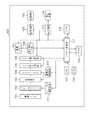
図1は、撮像装置100の構成を示すブロック図である。
図1において、101は撮像レンズである。102はフォーカスレンズである。フォーカスレンズ102は光軸方向に位置を変えることで、焦点が調節される。103はCCDセンサ等からなる撮像素子である。撮像素子103は撮像レンズ101を通過した被写体像の光束を光電変換し、電気信号に変換する。
Embodiments of the present invention will be described below with reference to the drawings.
FIG. 1 is a block diagram illustrating a configuration of the
In FIG. 1,
104はCDS/AD部である。CDS/AD部104は撮像素子103から出力されたアナログ信号にクランプ処理及びゲイン処理等を行い、デジタル信号に変換する。111はフォーカス駆動回路である。フォーカス駆動回路111はフォーカスレンズ102を制御する。
105はスミア検出回路である。スミア検出回路105はシステム制御部117の制御の下、CDS/AD部104において変換されたデジタル信号(画像信号)からスミア信号を検出すると共にスミア信号におけるスミア量を検出する。スミア検出回路105は撮像素子103の光学的遮光画素であるOB(オプティカルブラック)画素領域及び/又は光による感度を有さないダミー画素領域に基づいてスミア信号を検出する。スミア検出回路105は検出結果を後述するスミア補正回路106及びシステム制御部117に送信する。なお、スミア検出回路105は画素領域のエリア毎にスミア量を送信する。スミア信号は主に遮光された垂直転送画素に電荷が重畳されることにより生じるノイズであるため、スミア検出回路105はOB画素領域やダミー画素領域から容易にスミア信号を検出することができる。
106はスミア補正回路である。スミア補正回路106はシステム制御部117の制御の下、検出されたスミア量に基づいてスミアを補正するためのスミア補正量を設定する。また、スミア補正回路106は設定したスミア補正量により画像信号のスミア補正を行う。
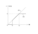
ここで、図2を参照してスミア補正回路106がスミア量に基づいて設定するスミア補正量について説明する。図2では、横軸が検出されたスミア量であり、縦軸が設定されるスミア補正量である。
図2に示す特性線301は従来のスミア量に基づいて設定するスミア補正量を示している。従来は特性線301に示すように、スミア量に比例してスミア補正量を設定している。従って、スミア量が大きくなるに従い、画像信号から大きなスミア補正量で減算してしまうために、スミアの発生が少ない画素では、大きなスミア補正量による過補正により画像信号を小さくなりすぎて、画質が低下してしまう。
Here, the smear correction amount set by the
A
一方、図2に示す特性線302は本実施形態に係るスミア量に基づいて設定するスミア補正量を示している。特性線302では、スミア量が極めて少ない範囲(図2に示す0からT1の範囲)の場合、スミア補正回路106はスミア補正量を下限値(ここでは、スミア補正量を0としている)に制限して設定する。また、スミア量が所定の量の範囲(図2に示すT1からT2の範囲)の場合、スミア補正回路106はスミア量に比例したスミア補正量を設定する。さらに、スミア量が所定値以上(図2に示すT2以上)の場合、スミア補正量を上限値(ここでは、スミア補正量をRとしている)に制限して設定する。このように、スミア量が大きくても、スミア補正量を上限値で制限することに、過補正による画質の低下を防止することができる。
On the other hand, a
また、スミア補正回路106は有効画素領域内の任意の画像エリアでスミア補正することができる。すなわち、スミア補正回路106はスミア量に応じて画像エリア毎に適応的にスミア補正量を設定することができる。
ここで、図3を参照して、画像エリア毎にスミア量が異なる画像について説明する。図3は、高輝度の被写体を撮像した画像の一例を示す図である。図3に示す画像のうち、補正領域501は黒い被写体があるためにスミア信号が少ない領域である。また、補正領域502は青空に広く薄いスミア信号が重畳している領域である。また、補正領域503は太陽等の高輝度被写体があるために強いスミア信号が重畳している領域である。スミア補正回路106は画像エリア毎、すなわち補正領域501、補正領域502及び補正領域503毎にスミア補正量を設定してスミア補正を行う。
Further, the
Here, with reference to FIG. 3, an image having a different smear amount for each image area will be described. FIG. 3 is a diagram illustrating an example of an image obtained by imaging a high-luminance subject. In the image shown in FIG. 3, the correction area 501 is an area where the smear signal is small because there is a black subject. The correction area 502 is an area where a wide and thin smear signal is superimposed on the blue sky. The correction area 503 is an area where a strong smear signal is superimposed because there is a high brightness subject such as the sun. The
具体的には、スミア補正回路106はスミア信号が少ない補正領域501には、スミア補正量を図2に示す下限値に設定してスミア補正を行う。また、スミア信号が薄い補正領域502には、スミア量に比例したスミア補正量に設定してスミア補正を行う。また、スミア信号が強い補正領域503には、スミア補正量を図2に示す上限値に設定してスミア補正を行う。このように、検出されたスミア量に応じたスミア補正を行うことで、最適なスミア補正をすることができる。特に、スミア信号が強い場合にはスミア補正量を上限値に制限して設定するため、過補正により画像信号が小さくなることを防止することができる。また、画像エリア毎にスミア補正を行うことで、画像エリアに適したスミア補正を行うことができる。
Specifically, the
図1のブロック図に戻り、108は信号処理回路である。信号処理回路108はスミア補正回路106によりスミア補正が行なわれた画像信号又はシステム制御部117からの画像信号に対してホワイトバランス処理、画素補間処理、色信号処理、輝度信号処理及び色ゲイン調整等の画像処理を行う。
ここで、上述したスミア補正回路106では過補正により画像信号が小さくなることを防止するために、スミア信号が強い場合にはスミア補正量を上限値に制限して設定した。したがって、スミア補正としては不十分であり、画像にスミアが残るおそれがある。そこで、信号処理回路108ではスミア量に基づいて、スミアを目立たなくする画像処理を行う。すなわち、スミアにはマゼンダの色成分を含んでいるために、信号処理回路108はスミア量に応じてマゼンダの色成分を緩和するようにホワイトバランス処理を行う。
Returning to the block diagram of FIG. 1,
Here, in the
ここで、図4を参照して、信号処理回路108がスミア量に基づいて画像処理(ホワイトバランス処理)を行う場合について説明する。図4では、横軸が検出されたスミア量であり、縦軸が設定されるホワイトバランス補正量である。図4では、スミア量に応じたホワイトバランス補正量の1次元ルックアップテーブルが示されている。なお、図4に示す横軸のT1及びT2は図2に示す横軸のT1及びT2に対応している。
Here, a case where the
図4に示す特性線401は外光の色温度が通常の場合のスミア量に応じたホワイトバランス補正量の1次元ルックアップテーブルを示している。特性線401に示すように、スミア量が所定の量の範囲(図4に示す0からT2近傍の範囲)の場合、信号処理回路108はホワイトバランス補正量を0に設定する。また、スミア量が所定量以上(図4に示すT2近傍より大きい範囲)の場合、信号処理回路108はスミア量に比例してグリーンのホワイトバランス補正量を設定、すなわち色ゲイン調整してホワイトバランス処理を行う。このように、スミア量に比例したグリーンのホワイトバランス補正量でホワイトバランス処理を行うことで、画質を低下させることなくスミアを補正することができる。
A
また、図4に示す特性線402は外光の色温度が快晴のときの日陰や曇り等の高色温度光源の場合のスミア量に応じたホワイトバランス補正量の1次元ルックアップテーブルを示している。高色温度光源の場合、青味の色成分が強くなる。したがって、特性線402では、青味の色成分を緩和させるためにマゼンタがホワイトバランス補正量に設定されるように、特性線401をマゼンタ側に略平行移動させた1次元ルックアップテーブルとしている。特性線402に示すように、スミア量が所定の量の範囲(図4に示す0からT2近傍の範囲)の場合、信号処理回路108はマゼンタ側の所定値にホワイトバランス補正量を設定して、ホワイトバランス処理を行う。また、スミア量が所定量以上(図4に示すT2近傍より大きい範囲)の場合、信号処理回路108はスミア量に比例してマゼンタ又はグリーンのホワイトバランス補正量を設定して、ホワイトバランス処理を行う。
A
外光の色温度はシステム制御部117が信号処理回路108において画像処理される画像信号の画像情報により算出する。信号処理回路108は算出された外光の色温度の結果に応じ、通常の色温度の場合は特性線401を用いて画像処理を行い、高色温度光源の場合は特性線402を用いて画像処理を行う。
なお、信号処理回路108ではスミア補正回路106における処理と同様、図3で上述したようにスミア量が異なる画像エリア毎に画像処理を行う。このように、画像エリア毎に画像処理を行うことで、画像エリアに適した画像処理を行うことができる。
The color temperature of the external light is calculated by the
Note that the
図1のブロック図に戻り、107は画像メモリである。システム制御部117は信号処理回路108において画像処理された画像信号を画像データとして画像メモリ107に記憶する。この画像メモリ107は撮像した所定枚数の静止画像や所定時間分の動画像を格納するのに十分に高速で、大量の記憶量を備えている。なお、画像メモリ107はシステム制御部117の作業領域としても使用される。
Returning to the block diagram of FIG. 1,
109は記録回路である。記録回路109は後述する記憶媒体110とのインタフェースである。記録回路109は記憶媒体110との間で画像データや画像データに付属する管理情報を送受信する。
110は取り外し可能なメモリカードやハードディスク等の記憶媒体である。記録回路109は画像メモリ107で記憶されている画像データを記憶媒体110に記録する。
114はLCD等の表示装置である。表示装置114には撮像した画像データが表示される。また、表示装置114に撮像した画像データを逐次表示することにより電子ファインダとしても使用することができる。
113は表示回路である。表示回路113は表示装置114に撮像した画像データ等を表示する制御を行う。また、表示回路113はシステム制御部117の制御の下、プログラムの実行に基づいて表示装置114に対する表示のオン、オフ、測距枠表示、合焦表示及び非合焦の警告表示等を行う。
119はRAMである。RAM119には表示装置114に表示されるデータが記憶される。表示回路113はシステム制御部117の制御の下、RAM119に記憶されたデータを表示装置114に表示する。118はROMである。なお、ROM118及びRAM119にはシステム制御部117の動作用の定数、変数及びプログラム等が記憶されている。
115はスイッチ(SW1)である。116はスイッチ(SW2)である。ユーザはスイッチ115及びスイッチ116を介して、静止画記録及び動画記録の開始の操作をしたり、停止等の操作をしたりすることができる。
117はシステム制御部である。システム制御部117は撮像装置100全体を制御する。また、システム制御部117は撮像レンズ101内の絞り及びシャッターを制御することにより自動露出制御(AE)を行ったり、フォーカス駆動回路111を制御することによりオートフォーカス(AF)を行ったりする。
次に、図5に示すフローチャートを参照して、撮像装置100の処理動作について説明する。以下の各ステップでは、システム制御部117以外が主体となって処理を行う場合、その主体はシステム制御部117の制御の下で処理を行う。
まず、ステップS1において、システム制御部117はOB領域からの信号出力値を所定の値に設定する(黒信号レベル設定)。例えば、最大出力14BitのCDS/ADを用いる場合、最大出力信号は16383LSBとなる。一例として、システム制御部117はOB画素出力値とダミー画素出力値とを最大出力値の5%(819LSB)となるようにCDS/ADを調整する。OB画素出力値とダミー画素出力値とは、スミア等のノイズ信号が重畳しなければ常に調整された値が出力される。
Next, the processing operation of the
First, in step S1, the
次に、ステップS2において、スミア検出回路105はスミア信号を検出する。スミア信号はOB画素出力値とダミー画素出力値とに重畳されたノイズ信号であることから、スミア検出回路105はOB信号、ダミー信号から調整した値を減算することで、スミア量を検出する。この処理はスミア検出手段の処理の一例に対応する。なお、本実施形態では、スミア検出回路105は1〜15564LSBの範囲のスミア量を検出可能である。なお、スミア検出回路105は検出されたスミア量に応じて画像エリアを分割する処理を行う。以下のステップでは、分割された画像エリア毎に処理が行なわれる。
Next, in step S2, the
次に、ステップS3において、スミア補正回路106はスミア検出回路105において検出されたスミア量が第一の所定範囲内であるか否かを判定する。例えば図2に示す特性線302の場合、スミア補正回路106はスミア量が図2に示す0からT1の範囲内であるか否かを判定する。このステップS3の判定によって、後述するホワイトバランス処理や色処理パラメータ等、画質に関するパラメータを補正するか否かが分かれる。スミア量が第一の所定範囲内である場合、システム制御部117はステップS4に処理を進める。スミア量が第一の所定範囲内ではない場合、システム制御部117はステップS6に処理を進める。
Next, in step S3, the
ステップS4において、スミア補正回路106はスミア補正量を所定の下限値に設定する(下限値クリップ処理)。続いて、スミア補正回路106は設定したスミア補正量によりスミア補正を行う。例えば図2に示す特性線302の場合、スミア補正量は0であるためスミア補正回路106はスミア補正を行わない。
In step S4, the
次に、ステップS5において、信号処理回路108は所定の下限値でスミア補正された画像信号に対して通常の画像処理を行う(通常画像処理)。このとき、システム制御部117では信号処理回路108で処理される画像信号の外光の色温度を検出する。この処理は色温度検出手段の一例に対応する。
信号処理回路108は検出された色温度からホワイトバランス処理を行うときのホワイトバランス補正量等を設定する。例えば、通常の光源であった場合、信号処理回路108は図4に示す特性線401(スミア量が0からT1の範囲)に基づき、ホワイトバランス補正量を0に設定する。また、高色温度光源であった場合、信号処理回路108は図4に示す特性線402に基づき、マゼンタが強くなるようにホワイトバランス補正量を設定してホワイトバランス処理を行う。また、信号処理回路108は画素補間処理等の通常の画像処理を行う。
Next, in step S5, the
The
ステップS6において、スミア補正回路106はスミア検出回路105において検出されたスミア量から、スミア補正を完全に行うことができるか否かを判定する。ここでは、スミア補正回路106はスミア量が第二の所定範囲内であるか否かを判定する。例えば、図2の示す特性線302の場合、スミア補正回路106はスミア量が図2に示すT1からT2の範囲内であるか否かを判定する。スミア量が第二の所定範囲内である場合、ステップS7に処理を進める。スミア量が第二の所定範囲内でない場合、ステップS8に処理を進める。
In step S <b> 6, the
ステップS7において、スミア補正回路106はスミア量に応じたスミア補正量を画像信号から減算してスミア補正を行う。図2に示す特性線302の場合、スミア量に比例したスミア補正量によりスミア補正を行う。続いて、信号処理回路108はステップS5と同様にスミア補正が行われた画像信号に対して画像処理を行う。
In step S7, the
ステップS8において、スミア補正回路106はスミア補正量を所定の上限値に設定する(上限値クリップ処理)。続いて、スミア補正回路106は設定したスミア補正量によりスミア補正を行う。例えば図2に示す特性線302の場合、スミア補正量の上限値はRであるため、スミア補正回路106はスミア補正量をRにしてスミア補正を行う。
In step S8, the
次に、ステップS9において、信号処理回路108は所定の上限値でスミア補正された画像信号に対して画像処理を行う(適応信号処理)。このとき、システム制御部117では、信号処理回路108で処理される画像信号の外光の色温度を検出する。この処理は色温度検出手段の一例に対応する。
信号処理回路108は検出された色温度からホワイトバランス処理を行うときのホワイトバランス補正量等を設定する。例えば、通常の光源であった場合、信号処理回路108は図4に示す特性線401(スミア量がT2より大きい範囲)に基づき、検出されたスミア量に応じてグリーンが強くなるようにホワイトバランス補正量を設定してホワイトバランス処理を行う。また、高色温度光源であった場合、信号処理回路108は図4に示す特性線402に基づき、検出されたスミア量に比例してマゼンタが弱くなるようにホワイトバランス補正量を設定してホワイトバランス処理を行う。また、所定のスミア量を超えた場合はスミア量に比例してグリーンが強くなるようにホワイトバランス補正量を設定してホワイトバランス処理を行う。
さらに、信号処理回路108は検出されたスミア量に応じて、色信号処理等の画質に関するパラメータを最適な値に設定して、画像処理を行う。
Next, in step S9, the
The
Furthermore, the
同様に、ステップS2により分割した画像エリア毎に、上述したステップS3からステップS9の処理を行う。このように、分割した画像エリア毎にスミア補正や画像処理を行うことにより、各画像エリア毎に最適なスミア補正及び画像処理を行うことができる。 Similarly, the processing from step S3 to step S9 described above is performed for each image area divided in step S2. In this way, by performing smear correction and image processing for each divided image area, it is possible to perform optimum smear correction and image processing for each image area.
上述したように本実施形態によれば、検出したスミア量が所定値より大きい場合には、スミア補正量を上限値に設定してスミア補正を行うことで、過補正により画像信号が小さくなりすぎることを防止することができる。一方、上限値を設定することによりスミア補正が十分に行えないとしても、検出されたスミア量に基づいてホワイトバランス処理を行いスミアの補正を補うために、スミアを目立たないようにすることができる。なお、本実施形態では、検出したスミア量に基づいて、スミア補正及び画像処理を行う場合についてのみ説明したが、この場合に限られない。例えば、信号処理回路108はスミア補正量に基づいて画像処理を行ってもよい。
As described above, according to the present embodiment, when the detected smear amount is larger than the predetermined value, the smear correction amount is set to the upper limit value and the smear correction is performed, so that the image signal becomes too small due to overcorrection. This can be prevented. On the other hand, even if the smear correction cannot be sufficiently performed by setting the upper limit value, the smear can be made inconspicuous in order to compensate for the smear correction by performing the white balance processing based on the detected smear amount. . In the present embodiment, only the case of performing smear correction and image processing based on the detected amount of smear has been described, but the present invention is not limited to this case. For example, the
上述した本発明の実施形態における撮像装置を構成する各手段、又は撮像装置の画像処理方法の各ステップは、コンピュータのRAMやROM等に記憶されたプログラムが動作することによっても実現できる。このプログラム及びこのプログラムを記録したコンピュータ読み取り可能な記録媒体は本発明に含まれる。 Each means constituting the image pickup apparatus or each step of the image processing method of the image pickup apparatus in the embodiment of the present invention described above can also be realized by operating a program stored in a RAM or ROM of a computer. This program and a computer-readable recording medium on which this program is recorded are included in the present invention.
また、本発明は、例えば、システム、装置、方法、プログラムもしくは記録媒体等としての実施形態も可能であり、具体的には、複数の機器からなるシステムに適用してもよい。 In addition, the present invention can be implemented as, for example, a system, apparatus, method, program, or recording medium. Specifically, the present invention may be applied to a system including a plurality of devices.
なお、本発明は、上述した実施形態の機能を実現するソフトウェアのプログラムを、システム又は装置に直接、又は遠隔から供給する。そして、そのシステム又は装置のコンピュータが前記供給されたプログラムコードを読み出して実行することによっても達成される場合を含む。 The present invention supplies a software program for realizing the functions of the above-described embodiments directly or remotely to a system or apparatus. In addition, this includes a case where the system or the computer of the apparatus is also achieved by reading and executing the supplied program code.
従って、本発明の機能処理をコンピュータで実現するために、前記コンピュータにインストールされるプログラムコード自体も本発明を実現するものである。つまり、本発明は、本発明の機能処理を実現するためのコンピュータプログラム自体も含まれる。その場合、プログラムの機能を有していれば、オブジェクトコード、インタプリタにより実行されるプログラム、OSに供給するスクリプトデータ等の形態であってもよい。 Accordingly, since the functions of the present invention are implemented by computer, the program code installed in the computer also implements the present invention. In other words, the present invention includes a computer program itself for realizing the functional processing of the present invention. In that case, as long as it has the function of a program, it may be in the form of object code, a program executed by an interpreter, script data supplied to the OS, and the like.
また、コンピュータが、読み出したプログラムを実行することによって、一前述した実施形態の機能が実現される。更に、そのプログラムの指示に基づき、コンピュータ上で稼動しているOS等が、実際の処理の一部又は全部を行い、その処理によっても前述した実施形態の機能が実現され得る。 Further, the functions of the above-described embodiment are realized by the computer executing the read program. Furthermore, based on the instructions of the program, an OS or the like running on the computer performs part or all of the actual processing, and the functions of the above-described embodiments can be realized by the processing.
さらに、その他の方法として、まず記録媒体から読み出されたプログラムが、コンピュータに挿入された機能拡張ボードやコンピュータに接続された機能拡張ユニットに備わるメモリに書き込まれる。そして、そのプログラムの指示に基づき、その機能拡張ボードや機能拡張ユニットに備わるCPU等が実際の処理の一部又は全部を行い、その処理によっても前述した実施形態の機能が実現される。 As another method, the program read from the recording medium is first written in a memory provided in a function expansion board inserted into the computer or a function expansion unit connected to the computer. Then, based on the instructions of the program, the CPU or the like provided in the function expansion board or function expansion unit performs part or all of the actual processing, and the functions of the above-described embodiments are realized by the processing.
100 撮像装置
101 撮影レンズ
102 フォーカスレンズ
103 撮像素子
104 CDS/AD
105 スミア検出回路
106 スミア補正回路
107 画像メモリ
108 信号処理回路
109 記録回路
110 記録媒体
112 撮像部駆動回路
113 表示回路
114 表示装置
115 SW1
116 SW2
117 システム制御部
118 ROM
119 RAM
DESCRIPTION OF
DESCRIPTION OF
116 SW2
117
119 RAM
Claims (11)
画像信号からスミア量を検出するスミア検出手段と、
前記スミア検出手段により検出されたスミア量に基づいて、分割領域ごとにスミア補正を行うスミア補正手段と、
前記スミア検出手段により検出されたスミア量が、前記スミア補正手段が設定するスミア補正量の上限値を超える場合に、スミアによる画像の色の変化を軽減するホワイトバランス処理を、前記分割領域ごとに行う画像処理手段とを有することを特徴とする撮像装置。 An imaging apparatus capable of correcting smear that occurs in a captured image,
Smear detecting means for detecting a smear amount from the image signal;
Smear correction means for performing smear correction for each divided region based on the smear amount detected by the smear detection means;
When the smear amount detected by the smear detection unit exceeds the upper limit value of the smear correction amount set by the smear correction unit, white balance processing for reducing the color change of the image due to smear is performed for each divided region. An image pickup apparatus comprising: an image processing means for performing.
前記画像処理手段は、前記スミア検出手段により検出されたスミア量及び前記色温度検出手段により検出された色温度に基づいて、画像処理を行うことを特徴とする請求項1乃至4の何れか1項に記載の撮像装置。 It further has color temperature detection means for performing color temperature detection,
5. The image processing unit according to claim 1, wherein the image processing unit performs image processing based on a smear amount detected by the smear detection unit and a color temperature detected by the color temperature detection unit. The imaging device according to item.
前記スミア補正手段は、前記スミア検出手段により検出された画像エリア毎にスミア補正を行うことを特徴とする請求項1乃至5の何れか1項に記載の撮像装置。 The smear detection means detects an image area where smear has occurred,
The imaging apparatus according to claim 1, wherein the smear correction unit performs smear correction for each image area detected by the smear detection unit.
画像信号からスミア量を検出するスミア検出ステップと、
前記スミア検出ステップにより検出されたスミア量に基づいて、分割領域ごとにスミア補正を行うスミア補正ステップと、
前記スミア検出ステップにより検出されたスミア量が、前記スミア補正ステップにて設定されるスミア補正量の上限値を超える場合に、スミアによる画像の色の変化を軽減するホワイトバランス処理を、前記分割領域ごとに行う画像処理ステップとを有することを特徴とする画像処理方法。 An image processing method of an imaging apparatus capable of correcting smear generated in a captured image,
A smear detection step for detecting a smear amount from the image signal;
A smear correction step for performing smear correction for each divided region based on the smear amount detected by the smear detection step;
When the smear amount detected in the smear detection step exceeds the upper limit value of the smear correction amount set in the smear correction step, white balance processing for reducing the color change of the image due to smear is performed in the divided area. And an image processing step performed for each .
画像信号からスミア量を検出するスミア検出ステップと、
前記スミア検出ステップにより検出されたスミア量に基づいて、分割領域ごとにスミア補正を行うスミア補正ステップと、
前記スミア検出ステップにより検出されたスミア量が、前記スミア補正ステップにて設定されるスミア補正量の上限値を超える場合に、スミアによる画像の色の変化を軽減するホワイトバランス処理を、前記分割領域ごとに行う画像処理ステップとをコンピュータに実行させるためのプログラム。 A program for controlling an image pickup apparatus capable of correcting smear generated in a picked-up image,
A smear detection step for detecting a smear amount from the image signal;
A smear correction step for performing smear correction for each divided region based on the smear amount detected by the smear detection step;
When the smear amount detected in the smear detection step exceeds the upper limit value of the smear correction amount set in the smear correction step, white balance processing for reducing the color change of the image due to smear is performed in the divided area. A program for causing a computer to execute an image processing step to be performed every time .
Priority Applications (3)
| Application Number | Priority Date | Filing Date | Title |
|---|---|---|---|
| JP2008167871A JP5268448B2 (en) | 2008-06-26 | 2008-06-26 | Imaging apparatus, image processing method thereof, and program |
| US12/490,319 US8218040B2 (en) | 2008-06-26 | 2009-06-24 | Image processing apparatus, image processing method and computer-readable storage medium |
| CN2009101422423A CN101616254B (en) | 2008-06-26 | 2009-06-26 | Image processing apparatus and image processing method |
Applications Claiming Priority (1)
| Application Number | Priority Date | Filing Date | Title |
|---|---|---|---|
| JP2008167871A JP5268448B2 (en) | 2008-06-26 | 2008-06-26 | Imaging apparatus, image processing method thereof, and program |
Publications (3)
| Publication Number | Publication Date |
|---|---|
| JP2010011073A JP2010011073A (en) | 2010-01-14 |
| JP2010011073A5 JP2010011073A5 (en) | 2011-08-04 |
| JP5268448B2 true JP5268448B2 (en) | 2013-08-21 |
Family
ID=41446915
Family Applications (1)
| Application Number | Title | Priority Date | Filing Date |
|---|---|---|---|
| JP2008167871A Expired - Fee Related JP5268448B2 (en) | 2008-06-26 | 2008-06-26 | Imaging apparatus, image processing method thereof, and program |
Country Status (3)
| Country | Link |
|---|---|
| US (1) | US8218040B2 (en) |
| JP (1) | JP5268448B2 (en) |
| CN (1) | CN101616254B (en) |
Families Citing this family (4)
| Publication number | Priority date | Publication date | Assignee | Title |
|---|---|---|---|---|
| US8953233B2 (en) * | 2010-06-14 | 2015-02-10 | Canon Kabushiki Kaisha | Image reading apparatus and image data processing method |
| KR102301620B1 (en) * | 2015-02-02 | 2021-09-14 | 삼성전자주식회사 | Photographing apparatus and method for the light leakage correction |
| EP4330915A1 (en) * | 2021-05-31 | 2024-03-06 | Shanghai United Imaging Healthcare Co., Ltd. | Systems and methods for image correction |
| CN113709372B (en) * | 2021-08-27 | 2024-01-23 | 维沃移动通信(杭州)有限公司 | Image generation method and electronic device |
Family Cites Families (18)
| Publication number | Priority date | Publication date | Assignee | Title |
|---|---|---|---|---|
| JPH04280579A (en) | 1991-03-08 | 1992-10-06 | Sony Corp | Smear correction circuit in image pickup signal processor |
| JPH04334274A (en) * | 1991-05-10 | 1992-11-20 | Sony Corp | Smear correction circuit |
| JP4192284B2 (en) * | 1998-01-13 | 2008-12-10 | 富士フイルム株式会社 | Digital still camera |
| US6809763B1 (en) * | 1999-08-02 | 2004-10-26 | Olympus Optical Co., Ltd. | Image pickup apparatus and method of correcting deteriorated pixel signal thereof |
| JP2002208003A (en) * | 2001-01-12 | 2002-07-26 | Mitsubishi Electric Corp | Device for binarizing image |
| US7580063B2 (en) * | 2002-05-07 | 2009-08-25 | Fujifilm Corporation | Digital camera for outputting image correction information |
| JP3788393B2 (en) * | 2002-06-10 | 2006-06-21 | ソニー株式会社 | Digital still camera device, video camera device and information terminal device |
| JP2004260699A (en) | 2003-02-27 | 2004-09-16 | Canon Inc | Imaging apparatus, imaging method, and program |
| JP2005303785A (en) | 2004-04-14 | 2005-10-27 | Sony Corp | White balance adjusting device, and white balance adjusting method |
| US7586527B2 (en) * | 2005-01-07 | 2009-09-08 | Mediatek Usa Inc | Detecting smear leakage in an image sensor exposed to a bright light source |
| JP4742652B2 (en) * | 2005-04-14 | 2011-08-10 | 富士フイルム株式会社 | Imaging device |
| JP2007110375A (en) * | 2005-10-13 | 2007-04-26 | Fujifilm Corp | Smear correction device |
| JP4768448B2 (en) * | 2006-01-13 | 2011-09-07 | 富士フイルム株式会社 | Imaging device |
| JP2007312169A (en) * | 2006-05-19 | 2007-11-29 | Matsushita Electric Ind Co Ltd | Imaging apparatus |
| US7847979B2 (en) * | 2006-07-07 | 2010-12-07 | Eastman Kodak Company | Printer having differential filtering smear correction |
| JP4899688B2 (en) * | 2006-07-26 | 2012-03-21 | カシオ計算機株式会社 | Imaging apparatus and smear false color reduction method thereof |
| JP4385060B2 (en) * | 2007-05-16 | 2009-12-16 | シャープ株式会社 | Solid-state imaging device and electronic information device |
| JP2009044367A (en) * | 2007-08-08 | 2009-02-26 | Fujifilm Corp | Imaging method and imaging apparatus |
-
2008
- 2008-06-26 JP JP2008167871A patent/JP5268448B2/en not_active Expired - Fee Related
-
2009
- 2009-06-24 US US12/490,319 patent/US8218040B2/en not_active Expired - Fee Related
- 2009-06-26 CN CN2009101422423A patent/CN101616254B/en not_active Expired - Fee Related
Also Published As
| Publication number | Publication date |
|---|---|
| US20090322914A1 (en) | 2009-12-31 |
| US8218040B2 (en) | 2012-07-10 |
| JP2010011073A (en) | 2010-01-14 |
| CN101616254B (en) | 2012-05-23 |
| CN101616254A (en) | 2009-12-30 |
Similar Documents
| Publication | Publication Date | Title |
|---|---|---|
| JP4768448B2 (en) | Imaging device | |
| JP5347707B2 (en) | Imaging apparatus and imaging method | |
| US8462234B2 (en) | Image pickup apparatus and dark current correction method therefor | |
| JP5123137B2 (en) | Imaging apparatus and imaging method | |
| JP6227084B2 (en) | Image processing apparatus, imaging apparatus, and image processing method | |
| US20080129860A1 (en) | Digital camera | |
| JP5526014B2 (en) | Imaging device | |
| JP5954623B2 (en) | Imaging apparatus and image processing method | |
| JP2009044367A (en) | Imaging method and imaging apparatus | |
| US8155472B2 (en) | Image processing apparatus, camera, image processing program product and image processing method | |
| JP5223686B2 (en) | Imaging apparatus and imaging method | |
| JP5268448B2 (en) | Imaging apparatus, image processing method thereof, and program | |
| JP2013135343A (en) | Imaging device | |
| JP6762365B2 (en) | Image processing equipment, image processing methods and programs | |
| JP7229728B2 (en) | Imaging device, its control method, and program | |
| JP2010103700A (en) | Imaging device and imaging method | |
| JP5535443B2 (en) | Image processing device | |
| JP2007028496A (en) | Image processing apparatus, image processing method, program and storage medium | |
| JP5979040B2 (en) | Imaging apparatus, imaging method, and program | |
| JP5307572B2 (en) | Imaging system, video signal processing program, and imaging method | |
| JP5404217B2 (en) | Imaging apparatus and control method thereof | |
| JP3206826U (en) | Image processing device | |
| JP6601062B2 (en) | Imaging control apparatus, imaging control method, and program | |
| JP2006157341A (en) | Smear correcting method and signal processor for solid-state imaging device, and imaging apparatus | |
| JP5208799B2 (en) | Imaging system, video signal processing program, and imaging method |
Legal Events
| Date | Code | Title | Description |
|---|---|---|---|
| A521 | Request for written amendment filed |
Free format text: JAPANESE INTERMEDIATE CODE: A523 Effective date: 20110622 |
|
| A621 | Written request for application examination |
Free format text: JAPANESE INTERMEDIATE CODE: A621 Effective date: 20110622 |
|
| A977 | Report on retrieval |
Free format text: JAPANESE INTERMEDIATE CODE: A971007 Effective date: 20120918 |
|
| A131 | Notification of reasons for refusal |
Free format text: JAPANESE INTERMEDIATE CODE: A131 Effective date: 20120925 |
|
| A521 | Request for written amendment filed |
Free format text: JAPANESE INTERMEDIATE CODE: A523 Effective date: 20121126 |
|
| TRDD | Decision of grant or rejection written | ||
| A01 | Written decision to grant a patent or to grant a registration (utility model) |
Free format text: JAPANESE INTERMEDIATE CODE: A01 Effective date: 20130409 |
|
| A61 | First payment of annual fees (during grant procedure) |
Free format text: JAPANESE INTERMEDIATE CODE: A61 Effective date: 20130507 |
|
| LAPS | Cancellation because of no payment of annual fees |