JP5262896B2 - Display method of plasma display device - Google Patents
Display method of plasma display device Download PDFInfo
- Publication number
- JP5262896B2 JP5262896B2 JP2009073094A JP2009073094A JP5262896B2 JP 5262896 B2 JP5262896 B2 JP 5262896B2 JP 2009073094 A JP2009073094 A JP 2009073094A JP 2009073094 A JP2009073094 A JP 2009073094A JP 5262896 B2 JP5262896 B2 JP 5262896B2
- Authority
- JP
- Japan
- Prior art keywords
- white balance
- light emission
- primary color
- color video
- display
- Prior art date
- Legal status (The legal status is an assumption and is not a legal conclusion. Google has not performed a legal analysis and makes no representation as to the accuracy of the status listed.)
- Expired - Fee Related
Links
Images


Abstract
Description
本発明は、入力された複数の原色映像信号に対応して発光回数または強度を制御してカラー表示を行う表示装置に関し、特に、赤、緑および青の三原色の蛍光体の発光回数を制御してカラー表示を行うプラズマディスプレイ装置におけるホワイトバランス補正技術に関する。 The present invention relates to a display device that performs color display by controlling the number or intensity of light emission corresponding to a plurality of input primary color video signals, and in particular, controls the number of light emission of phosphors of three primary colors of red, green, and blue. The present invention relates to a white balance correction technique in a plasma display device that performs color display.
近年、様々な表示装置の研究・開発が進められており、文字や映像等を鮮明に表示することができる大画面の平面型表示装置としてプラズマディスプレイ装置(プラズマディスプレイパネル:PDP(Plasma Display Panel)) が注目されている。このプラズマディスプレイ装置は、赤、緑および青の三原色の蛍光体により表示を行っているが、例えば、消費電力を制限するために画像の表示率(平均輝度レベル:APL(Average Picture Level))に応じて発光回数(維持発光の回数)を制御するようになっている。ところで、各蛍光体は、各発光回数に対する輝度比が一定ではなく、そのため、例えば、所定の発光回数でホワイトバランスの調整を行っても、発光回数が変化するとホワイトバランスもずれてしまうことになっていた。このホワイトバランスのずれの問題は、プラズマディスプレイ装置だけでなく、EL素子(エレクトロ・ルミネッセンス素子)を用いた表示装置やFED(Field Emission Display)、さらには、LED(Light Emitting Diode)ディスプレイやCRT(Cathode Ray Tube)等の様々な表示装置においてもその発光回数或いは強度の変化により生じる。そこで、入力された複数の原色映像信号に対応して発光回数または強度を制御してカラー表示を行う表示装置において、発光回数や強度に関わりなくホワイトバランスを維持することが要望されている。 In recent years, various display devices have been researched and developed, and plasma display devices (PDPs (Plasma Display Panels)) have been developed as flat display devices with large screens that can clearly display characters and images. ) Is attracting attention. This plasma display device performs display with phosphors of the three primary colors of red, green and blue. For example, in order to limit power consumption, the display rate of images (average luminance level: APL (Average Picture Level)) is used. Accordingly, the number of times of light emission (number of times of sustain light emission) is controlled. By the way, each phosphor does not have a constant luminance ratio with respect to the number of times of light emission. Therefore, for example, even if white balance is adjusted at a predetermined number of times of light emission, the white balance is also shifted when the number of times of light emission is changed. It was. The problem of this white balance shift is not only a plasma display device, but also a display device using an EL element (electroluminescence element), an FED (Field Emission Display), an LED (Light Emitting Diode) display, and a CRT (CRT). In various display devices such as Cathode Ray Tube), it is caused by the change in the number of times of light emission or intensity. Therefore, in a display device that performs color display by controlling the number of times or intensity of light emission corresponding to a plurality of input primary color video signals, it is desired to maintain white balance regardless of the number of times of light emission or intensity.
本願発明は、上述のように、プラズマディスプレイ装置だけでなく、EL素子を用いた表示装置やFEDおよびCRT等の様々な表示装置に適用することができるが、以下の説明では、赤、緑および青の三原色の蛍光体の間で残光特性の異なる表示装置として主にプラズマディスプレイ装置を例に取って説明する。 As described above, the present invention can be applied not only to a plasma display device but also to various display devices such as a display device using an EL element and FED and CRT. In the following description, red, green and A plasma display device will be mainly described as an example of a display device having different afterglow characteristics among the phosphors of the three primary colors of blue.
図1は面放電交流駆動型プラズマディスプレイ装置の一例を概略的に示すブロック図である。図1において、参照符号10は表示パネル、11はアドレス電極、12は走査・維持電極、13は維持電極、14はアドレス駆動回路、15は走査・維持パルス出力回路、16は維持パルス出力回路、17は駆動制御回路、18は信号処理回路、そして、19は隔壁を示している。
FIG. 1 is a block diagram schematically showing an example of a surface discharge AC drive type plasma display device. In FIG. 1,
図1に示されるように、プラズマディスプレイ装置は、アドレス電極11、走査・維持電極12、維持電極13および隔壁19を有する表示パネル10と、アドレス電極11を駆動するためのアドレス駆動回路14と、走査・維持電極12を駆動するための走査・維持パルス出力回路15と、維持電極を駆動するための維持パルス出力回路16と、これらの出力回路を制御する駆動制御回路17と、入力信号の処理を行う信号処理回路18と、を備えている。
As shown in FIG. 1, the plasma display device includes a
ここで、表示パネル10は、対向する2枚のガラス板の一方にアドレス電極11を設け、他方に走査・維持電極12および維持電極13を設けるようになっている。そして、これらガラス板に挟まれた空間が隔壁19によって仕切られ、その仕切られた各々の空間がそれぞれ放電セルを構成している。
Here, the
放電セルには、例えば、He−Xe、Ne−Xeのような希ガスが封入されており、走査・維持電極12と維持電極13とに電圧を加えると、放電が起こり、紫外線が発生する。また、各々の放電セルには、赤、緑および青のいずれかに発光する蛍光体が塗布されており、上記のように発生した紫外線により、この蛍光体が励起してこの蛍光体に応じた色光を発光させる。この発光を利用し、映像信号に応じて所望の色の放電セルを選択することにより、カラー画像表示を行うことができる。
For example, a rare gas such as He—Xe or Ne—Xe is sealed in the discharge cell. When a voltage is applied to the scan / sustain
なお、駆動制御回路17は、映像信号(三原色映像信号R,G,B)による画像の表示率(或いは、表示電流)に従って、走査・維持パルス出力回路15および維持パルス出力回路16を介して映像信号の発光回数を制御して、消費電力が予め定められた値よりも大きくならないようにしている。
Note that the
図2は図1のプラズマディスプレイ装置における駆動シーケンスの一例を説明するための図であり、上述した発光原理を用いた時分割駆動法(以下、サブフィールド法と称する)を説明するためのものである。 FIG. 2 is a diagram for explaining an example of a driving sequence in the plasma display device of FIG. 1, for explaining a time-division driving method (hereinafter referred to as a subfield method) using the light emission principle described above. is there.
サブフィールド法とは、1フレームを発光回数の違いによって重み付けされた複数のサブフィールド(SF1〜SF4)に分割し、画素毎にそこでの信号の振幅に応じたサブフィールドを選択することで階調を表現する方法である。 In the subfield method, one frame is divided into a plurality of subfields (SF1 to SF4) weighted according to the difference in the number of times of light emission, and gradation is determined by selecting a subfield corresponding to the amplitude of the signal there for each pixel. Is a way of expressing.
図2に示すサブフィールド法による駆動シーケンスは、1フレームを4つのサブフィールドSF1〜SF4に分割して16階調を表示する場合の例を示している。各サブフィールドの走査期間T1は、そのサブフィールドでの発光する放電セル(以下、発光セルと称する)を選択するための期間であり、また、放電維持期間T2は、その選択された発光セルが発光している期間である。 The driving sequence by the subfield method shown in FIG. 2 shows an example in which one frame is divided into four subfields SF1 to SF4 and 16 gradations are displayed. The scanning period T1 of each subfield is a period for selecting a discharge cell (hereinafter referred to as a light emitting cell) that emits light in the subfield, and the discharge sustaining period T2 is a period for selecting the selected light emitting cell. This is the period during which light is emitted.
サブフィールドSF1〜SF4の放電維持期間T2は、選択されたセルが発光する時間を表し、各々は8:4:2:1の比率で発光回数に重み付けされている。そして、映像信号レベルに応じてこれらサブフィールドSF1〜SF4のいずれかを任意に選択することにより、2の4乗=16階調の表示が可能になる。階調数を増やしたい場合には、サブフィールドの数を増やせば良く、例えば、サブフィールド数を8とすると、2の8乗=256階調の表示が可能になる。なお、各サブフィールドの輝度レベルは維持発光の回数(発光回数)によって制御する。 The discharge sustain period T2 of the subfields SF1 to SF4 represents the time during which the selected cell emits light, and each is weighted to the number of times of light emission at a ratio of 8: 4: 2: 1. Then, by arbitrarily selecting any one of these subfields SF1 to SF4 according to the video signal level, it is possible to display 2 4 = 16 gradations. In order to increase the number of gradations, the number of subfields may be increased. For example, when the number of subfields is 8, display of 2 8 = 256 gradations is possible. Note that the luminance level of each subfield is controlled by the number of times of sustain light emission (number of light emission times).
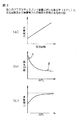
図3は図1のプラズマディスプレイ装置における表示率(APL)と発光回数および消費電力との関係を説明するための図であり、図3(a)は発光セルの発光回数と消費電力の関係を示し、図3(b)は画像(表示パネル)の表示率(APL)と発光回数の関係を示し、そして、図3(c)は映像信号による画像の表示率と消費電力の関係を示している。 FIG. 3 is a diagram for explaining the relationship between the display rate (APL), the number of times of light emission, and the power consumption in the plasma display device of FIG. 1, and FIG. 3 (a) shows the relationship between the number of times of light emission of the light emitting cell and the power consumption. 3 (b) shows the relationship between the display rate (APL) of the image (display panel) and the number of times of light emission, and FIG. 3 (c) shows the relationship between the display rate of the image by the video signal and the power consumption. Yes.
図3(a)に示されるように、プラズマディスプレイ装置の消費電力は、表示セルの発光回数の増加に従って増加する。そのため、実際のプラズマディスプレイ装置においては、図3(b)に示されるように、消費電力を予め定められた値以下に抑えるために、画像の表示率(APL)が高い場合、すなわち、画面全体で発光が行われるような画像(映像信号)が表示された場合には、前述した各サブフィールドの発光回数の重み付け比率を保持しながら、フレーム全体としての発光回数を制限するようになっている。 As shown in FIG. 3A, the power consumption of the plasma display device increases as the number of light emission times of the display cell increases. Therefore, in an actual plasma display device, as shown in FIG. 3B, in order to keep the power consumption below a predetermined value, the image display rate (APL) is high, that is, the entire screen. When an image (video signal) that emits light is displayed, the number of times of light emission as a whole frame is limited while maintaining the weighting ratio of the number of times of light emission of each subfield described above. .
つまり、図3(b)において、表示階調数を256階調とした場合、例えば、A点での発光回数は、512:256:128:64:32:16:8:4の重み付けであるとすれば、1020回であり、また、B点での発光回数は128:64:32:16:8:4:2:1の重み付けであるとすれば、発光回数を255回に制限する。すなわち、図3(c)に示されるように、発光回数をAPLに応じて制限することで、APLが高くなってもプラズマディスプレイ装置の消費電力を抑えるようになっている。 That is, in FIG. 3B, when the number of display gradations is 256 gradations, for example, the number of times of light emission at point A is a weight of 512: 256: 128: 64: 32: 16: 8: 4. If it is, it is 1020 times, and if the number of times of light emission at point B is weighted 128: 64: 32: 16: 8: 4: 2: 1, the number of times of light emission is limited to 255 times. That is, as shown in FIG. 3C, the power consumption of the plasma display device is suppressed even when the APL increases by limiting the number of times of light emission according to the APL.
図4は従来のホワイトバランス調整回路の一例を示すブロック図である。図4において、参照符号11〜13は乗算器、2はマイクロコンピュータ(マイコン)、そして、41〜43はγ補正回路を示している。
FIG. 4 is a block diagram showing an example of a conventional white balance adjustment circuit. In FIG. 4,
図4に示されるように、従来のホワイトバランス調整回路は、入力された映像信号R,G,Bをそれぞれガンマ補正回路41〜43によりガンマ補正し、その後、各乗算器11〜13により、マイコン2からの乗算係数(振幅係数)Kr,Kg,Kbを乗算する。すなわち、マイコン2は、赤、緑および青の輝度比を変えてホワイトバランスを調整するために各色の映像信号R,G,B用の係数Kr,Kg,Kbを乗算器11〜13に与える。ここで、係数Kr,Kg,Kbは、各色の映像信号R,G,Bにより同じ場合もあり、また、異なる場合もある。すなわち、従来のホワイトバランス調整回路は、マイコン2からの係数Kr,Kg,Kbを乗算器11〜13に与えて、各色の映像信号R,G,Bの信号振幅を制御することでホワイトバランスの調整を行う。
As shown in FIG. 4, the conventional white balance adjustment circuit performs gamma correction on input video signals R, G and B by
ここで、従来のホワイトバランス調整回路では、ホワイトバランスを調整するために、例えば、所定の発光回数において、或る一定の調整パターン(例えば、ウィンドウパターン等)を表示させて所望のホワイトバランスが得られるように、各色の映像信号R,G,Bの信号振幅調整を行う。すなわち、例えば、工場出荷の前に、各セット(プラズマディスプレイ装置)毎にホワイトバランスを調整するが、一定の調整パターンを所定の発光回数において表示させ、その状態でマイコン2のレジスタに係数Kr,Kg,Kbを設定するようになっている。 Here, in the conventional white balance adjustment circuit, in order to adjust the white balance, for example, a predetermined adjustment pattern (for example, a window pattern) is displayed at a predetermined number of times of light emission to obtain a desired white balance. As shown, the signal amplitudes of the video signals R, G, and B of the respective colors are adjusted. That is, for example, before factory shipment, the white balance is adjusted for each set (plasma display device), but a fixed adjustment pattern is displayed at a predetermined number of times of light emission, and in that state, the coefficient Kr, Kg and Kb are set.
上述したように、従来のホワイトバランス調整回路では、所定のAPL(すなわち、所定の発光回数)において或る一定の調整パターンを表示してホワイトバランスを調整するため、異なる発光回数(APL)ではホワイトバランスがずれることがある。 As described above, in the conventional white balance adjustment circuit, the white balance is adjusted by displaying a certain adjustment pattern at a predetermined APL (that is, a predetermined number of times of light emission). Balance may be off.
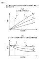
図5は赤、緑および青の三原色の各蛍光体の発光回数と輝度との関係を示す図であり、図5(a)は発光回数と輝度の関係を示し、また、図5(b)はエネルギー変換効率の減少による単位発光輝度特性を示す。 FIG. 5 is a diagram showing the relationship between the number of times of light emission and the luminance of the phosphors of the three primary colors of red, green and blue. FIG. 5 (a) shows the relationship between the number of times of light emission and the luminance, and FIG. Indicates unit luminance characteristics due to a decrease in energy conversion efficiency.
図5(a)に示されるように、赤、緑および青の三原色の各蛍光体は、発光回数が増加するに従って輝度が飽和してくる。これは、赤、緑および青の蛍光体の残光特性、言い換えれば、紫外線による励起に対する蛍光体のエネルギー変換効率が、図5(b)に示すように、発光回数の増加に従って低下するために生じるのである。なお、図5(b)における縦軸は、単位発光あたりの輝度を、エネルギー変換効率が最も高い場合の単位あたりの発光輝度で正規化した値を示し、また、横軸は、発光回数を示している。 As shown in FIG. 5A, the luminances of the three primary colors of red, green and blue become saturated as the number of times of light emission increases. This is because the afterglow characteristics of the phosphors of red, green and blue, in other words, the energy conversion efficiency of the phosphor with respect to excitation by ultraviolet rays decreases as the number of times of light emission increases as shown in FIG. It happens. In FIG. 5B, the vertical axis indicates the value obtained by normalizing the luminance per unit light emission with the light emission luminance per unit when the energy conversion efficiency is the highest, and the horizontal axis indicates the number of times of light emission. ing.
ここで、図5(a)および図5(b)において、例えば、発光回数が多いA点でホワイトバランスの調整を行ったとすると、その時のホワイトバランス値は、A点における赤、緑および青の輝度比によって決定する。しかしながら、APLが高い映像信号を表示する場合には、前述したように消費電力を予め定められた値以内に抑えるために、発光回数を減少させるようになっている。 Here, in FIG. 5A and FIG. 5B, for example, if the white balance is adjusted at point A where the number of times of light emission is large, the white balance value at that time is red, green and blue at point A. Determined by luminance ratio. However, when displaying a video signal with a high APL, as described above, the number of times of light emission is reduced in order to keep power consumption within a predetermined value.
従って、発光回数が少ないB点の場合には、図5(b)に示されるように、紫外線による励起に対する蛍光体のエネルギー変換効率が上がるため、エネルギー変換効率の減少率が緑>赤>青となっていれば、A点と比較して相対的に緑>赤>青の順に輝度が高くなる。すなわち、B点における赤、緑および青の輝度比は、A点での調整値と異なるために、A点とB点とではホワイトバランスに違いが生じる。 Therefore, in the case of point B where the number of times of light emission is small, as shown in FIG. 5 (b), the energy conversion efficiency of the phosphor with respect to excitation by ultraviolet light increases, so the rate of decrease in energy conversion efficiency is green> red> blue. If this is the case, the brightness is relatively higher in the order of green> red> blue than the point A. That is, since the luminance ratio of red, green, and blue at point B is different from the adjustment value at point A, there is a difference in white balance between point A and point B.
逆に、APLがホワイトバランス調整時よりも低い映像信号を表示する場合には、発光回数を増加させることがあるため、エネルギー変換効率がより一層低下して、発光回数が少ない場合と同様に赤、緑および青の輝度比が異なってホワイトバランス値に違いが生じる。 Conversely, when displaying a video signal whose APL is lower than that at the time of white balance adjustment, the number of times of light emission may be increased. Therefore, the energy conversion efficiency is further reduced, and red is emitted as in the case where the number of times of light emission is small. The brightness ratio of green and blue is different and the white balance value is different.
本発明は、上述した従来のホワイトバランス調整技術における課題に鑑み、発光回数や強度に関わりなくホワイトバランスを維持することができるホワイトバランス補正回路および補正方法、並びに、表示装置の提供を目的とする。 The present invention has been made in view of the above-described problems in the conventional white balance adjustment technology, and provides a white balance correction circuit, a correction method, and a display device capable of maintaining white balance regardless of the number of times of light emission and the intensity. .
本発明の一実施の態様は、例えば特許請求の範囲に記載された技術的思想を用いればよい。 In one embodiment of the present invention , for example, the technical idea described in the claims may be used.
本発明によれば、発光回数や強度に関わりなくホワイトバランスを維持することができる。 According to the present invention, white balance can be maintained regardless of the number of times of light emission and intensity.
以下、本発明に係るホワイトバランス補正回路および補正方法、並びに、表示装置の各実施例を図面を参照して詳述する。なお、以下の本実施例の説明では、プラズマディスプレイ装置を例にとっているが、本発明は、プラズマディスプレイ装置だけでなく、EL素子を用いた表示装置やFEDおよびLEDディスプレイやCRT等の様々な表示装置に適用することができる。 Embodiments of a white balance correction circuit, a correction method, and a display device according to the present invention will be described below in detail with reference to the drawings. In the following description of the present embodiment, a plasma display device is taken as an example. However, the present invention is not limited to a plasma display device, but various displays such as a display device using an EL element, an FED, an LED display, and a CRT. It can be applied to the device.
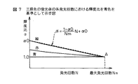
図6は本発明に係るホワイトバランス補正回路の第1実施例を示すブロック図であり、図7は三原色の蛍光体の各発光回数における輝度比を青色を基準として示す図である。 FIG. 6 is a block diagram showing a first embodiment of the white balance correction circuit according to the present invention, and FIG. 7 is a diagram showing the luminance ratio of each of the three primary color phosphors with respect to the number of times of light emission with reference to blue.
図6において、参照符号11〜13は乗算器、2はマイコン(マイクロコンピュータ)、そして、3はAPL検出回路(平均輝度レベル(表示率)検出回路)を示している。なお、参照符号Kr,Kg,Kbは、それぞれ入力された映像信号(ディジタルの三原色映像信号)R,G,Bに対する乗算係数(振幅係数)である。
In FIG. 6,
図6に示されるように、本第1実施例のホワイトバランス調整回路は、入力された映像信号R,G,Bをマイコン2から与えられた乗算係数Kr,Kg,Kbに従って乗算器11〜13を用いて振幅調整することでホワイトバランスを調整する。マイコン2は、APL検出回路3から得られたAPL(平均輝度レベル:表示率)に従って発光回数を設定する。さらに、マイコン2は、発光回数からエネルギー変換効率の増減によるR,G,B(赤、緑および青)の輝度比の増減率を演算し、その増減率を逆補正して赤、緑および青間で、輝度比が一定になるように乗算係数Kr,Kg,Kbを演算して各乗算器11〜13に供給する。
As shown in FIG. 6, the white balance adjustment circuit of the first embodiment includes
例えば、最大の発光回数の時にホワイトバランス調整を行い、それに合わせて各発光回数における補正を行うとし、青の蛍光体が最も残光特性が短い(つまり、エネルギー変換効率が減少しない)として、青の輝度を基準にした場合、各発光回数における赤、緑および青の輝度比が図7のような特性になるとする。このとき、青を基準にした輝度比をα、発光回数ゼロ時の輝度比をα0、発光回数をN、最大発光回数をNmとして緑の輝度比の変化を1次式で近似すると、α=((1−α0)/Nm)・N+α0という式が得られる。 For example, white balance adjustment is performed at the maximum number of times of light emission, and correction is performed for each number of times of light emission, and blue phosphor has the shortest afterglow characteristics (that is, energy conversion efficiency does not decrease). 7 is assumed to be a characteristic as shown in FIG. 7 with respect to the luminance ratio of red, green, and blue at each light emission number. At this time, assuming that the luminance ratio based on blue is α, the luminance ratio at the time of zero light emission is α0, the light emission number is N, the maximum light emission number is Nm, and the change of the green luminance ratio is approximated by a linear expression, α = The equation ((1−α0) / Nm) · N + α0 is obtained.
各発光回数において、ホワイトバランスを一定にするためには、輝度比の増減率を逆補正してやればよいから、乗算係数Kgは、輝度比αの逆数Kg=1/αとして算出することができる。さらに、赤(R)においても同様に算出することができる。もちろん、基準とする色を変えても同様である。このようにして乗算係数Kr,Kg,Kbをマイコン2によって演算し、乗算器1に設定して信号振幅を調整すれば、各発光回数において輝度比を一定に保つことが可能になり、ホワイトバランスを一定に維持することができる。また、ここでは1次式により近似を行ったが、より高次式で近似を行うことにより一層正確な補正を行うことも可能である。
In order to make the white balance constant at each number of times of light emission, it is only necessary to reversely correct the increase / decrease rate of the luminance ratio, so the multiplication coefficient Kg can be calculated as the reciprocal Kg = 1 / α of the luminance ratio α. Further, the same calculation can be made for red (R). Of course, the same applies even if the reference color is changed. If the multiplication coefficients Kr, Kg, and Kb are calculated by the
本実施例においては、まず、蛍光体の特性を把握するために発光回数と輝度の関係を予め測定し、例えば、図5(a)に示されるような発光回数と輝度の関係を得る。さらに、測定したデータから最もリニアな特性を有する蛍光体(例えば、青)を基準として各蛍光体(赤、緑および青)を正規化し、各発光回数における輝度比を算出する。 In this embodiment, first, in order to grasp the characteristics of the phosphor, the relationship between the number of times of light emission and the luminance is measured in advance, and for example, the relationship between the number of times of light emission and the luminance as shown in FIG. Further, each phosphor (red, green and blue) is normalized from the measured data on the basis of the phosphor having the most linear characteristics (for example, blue), and the luminance ratio at each light emission number is calculated.
すなわち、例えば、図7に示されるように、青を基準とし、この青に対する各蛍光体の輝度比を算出する。ここで、A点における赤、緑、青の輝度をそれぞれLar,Lag,Labとし、各発光回数における輝度をそれぞれLr,Lg,Lbとして正規化すると、次のようになる。なお、図7(実線:赤、緑、青)は、下記の式に基づいて算出した値を描いたものである。 That is, for example, as shown in FIG. 7, the luminance ratio of each phosphor with respect to blue is calculated using blue as a reference. Here, the red, green, and blue luminances at point A are normalized as Lar, Lag, and Lab, and the luminances at each light emission count are normalized as Lr, Lg, and Lb, respectively. Note that FIG. 7 (solid line: red, green, blue) depicts values calculated based on the following equations.
赤の青に対する輝度比=(Lr/Lar)/(Lb/Lab)
緑の青に対する輝度比=(Lg/Lag)/(Lb/Lab)
Luminance ratio of red to blue = (Lr / Lar) / (Lb / Lab)
Luminance ratio of green to blue = (Lg / Lag) / (Lb / Lab)
ところで、発光回数によるホワイトバランスの変動を抑制するには、輝度比が常に一定であればよいから、輝度比の変化を図7(破線:緑)に示すように1次式で近似し、その逆数(乗算係数K)を映像信号に乗算することでホワイトバランスを補正する。すなわち、K=1/α=Nm/(N+α0(Nm−N))という式により乗算係数Kを算出する。 By the way, in order to suppress the fluctuation of the white balance due to the number of times of light emission, it is sufficient that the luminance ratio is always constant. Therefore, the change of the luminance ratio is approximated by a linear expression as shown in FIG. White balance is corrected by multiplying the video signal by the reciprocal (multiplication coefficient K). That is, the multiplication coefficient K is calculated by the equation: K = 1 / α = Nm / (N + α0 (Nm−N)).
図8は図6のホワイトバランス補正回路における赤、緑および青の三原色の各乗算係数を説明するための図であり、K=1/α=Nm/(N+α0(Nm−N))という式から赤、緑、青の乗算係数Kr,Kg,Kbを算出して描いたものである。なお、参照符号Nは発光回数、Nmは最大発光回数、α0は最小発光回数時における輝度比を示す。 FIG. 8 is a diagram for explaining the multiplication coefficients of the three primary colors of red, green, and blue in the white balance correction circuit of FIG. 6, and from the equation K = 1 / α = Nm / (N + α0 (Nm−N)). It is drawn by calculating red, green and blue multiplication coefficients Kr, Kg and Kb. Reference symbol N indicates the number of times of light emission, Nm indicates the maximum number of times of light emission, and α0 indicates the luminance ratio at the time of the minimum number of times of light emission.
ここで、図7に示される1次式は、蛍光体によって決まるものであり、蛍光体が決まれば決定する。従って、予めその逆数を算出する演算式(図8参照)をマイコン2にプログラムしておき、そのプログラムを使用して各発光回数による乗算係数を演算する。
Here, the linear expression shown in FIG. 7 is determined by the phosphor, and is determined when the phosphor is determined. Accordingly, an arithmetic expression (see FIG. 8) for calculating the reciprocal number is programmed in the
図9は、このマイコン2により演算された乗算係数に従って乗算した結果、すなわち、図6のホワイトバランス補正回路により補正された三原色の蛍光体の各発光回数における輝度比を示す図である。図9から明らかなように、赤、緑、青(三原色)の蛍光体は、発光回数に関わりなく輝度比を一定に維持することができ、従って、発光回数に関わりなくホワイトバランスを維持することができることが判る。
FIG. 9 is a diagram showing the result of multiplication according to the multiplication coefficient calculated by the
具体的に、例えば、最大発光回数における緑および青の輝度をそれぞれ200cd/m2 および80cd/m2 とし、最小発光回数における輝度をそれぞれ60cd/m2 および20cd/m2 と仮定する。 Specifically, for example, the luminance of green and blue at the maximum number of emissions are the 200 cd / m 2 and 80 cd / m 2, it is assumed the luminance of the minimum number of emissions and, respectively 60 cd / m 2 and 20 cd / m 2.
このとき、最大発光回数時における青と緑の輝度比は、
青:緑=80:200=1:2.5
となる。
At this time, the luminance ratio of blue and green at the maximum number of flashes is
Blue: Green = 80: 200 = 1: 2.5
It becomes.
また、最小発光回数時における青と緑の輝度比は、
青:緑=20:60=1:3
となる。
The luminance ratio of blue and green at the minimum number of flashes is
Blue: Green = 20: 60 = 1: 3
It becomes.
従って、青に対する緑の輝度比は。1.2倍(3/2.5倍)になっており、これがα0であるから、その逆数である乗算係数Kは、 Therefore, the luminance ratio of green to blue is. Since it is 1.2 times (3 / 2.5 times) and this is α0, the multiplication coefficient K which is the reciprocal thereof is
K=1/α0=1/1.2=0.83
となる。すなわち、緑の映像信号(G)に関しては、その信号振幅に0.83を乗じて補正を行うことになる。なお、赤の映像信号(R)についても同様である。従って、前述した近似式を用いて各発光回数における乗算係数を演算し、それを映像信号に乗算することで発光回数に関わりなくホワイトバランスを維持することが可能になる。
K = 1 / α0 = 1 / 1.2 = 0.83
It becomes. In other words, the green video signal (G) is corrected by multiplying its signal amplitude by 0.83. The same applies to the red video signal (R). Therefore, it is possible to maintain the white balance regardless of the number of times of light emission by calculating a multiplication coefficient for each number of times of light emission using the above approximate expression and multiplying it by the video signal.
図10は図6のホワイトバランス補正回路におけるAPL検出回路3の一例を示すブロック図である。図10において、参照符号31および33は加算器、32および34はレジスタを示している。
FIG. 10 is a block diagram showing an example of the
図10に示されるように、例えば、入力された8ビットの映像信号は加算器31で加算され、水平同期信号Hに対応する1ライン毎の映像出力(輝度)がレジスタ32に格納される。さらに、レジスタ32からの各ライン毎の出力は、加算器33で加算され、垂直同期信号Vに対応する1画面毎の映像出力がレジスタ34に格納される。そして、表示する画像の平均輝度レベル(表示率)が算出されるようになっている。なお、このAPL検出回路3は、例えば、表示装置の消費電力を予め定められた値よりも小さくするために、APL(表示率)に従って発光回数を制御するために使用するものをそのまま適用することができ、他の様々な構成が可能である。
As shown in FIG. 10, for example, the input 8-bit video signal is added by the
図11は本発明に係るホワイトバランス補正回路の第2実施例を示すブロック図である。図11において、参照符号5は電流検出回路、6はパネル駆動回路、そして、7は発光回数制御回路を示している。
FIG. 11 is a block diagram showing a second embodiment of the white balance correction circuit according to the present invention. In FIG. 11,
図11に示されるように、本発明の第2実施例は、前述した図6に示す第1実施例におけるAPL検出回路3の代わりに電流検出回路5を設けたもので、電流検出回路5によりパネル駆動回路6の消費電流(表示電流)を検出し、すなわち、第1実施例の表示率に対応する表示電流を検出し、それに応じてマイコン2が乗算係数を演算するようになっている。なお、本第2実施例においては、各蛍光体の発光回数の制御も電流検出回路5からの出力をマイコン2で受け取って、例えば、表示装置の消費電力が予め定められた値よりも小さくなるように発光回数制御回路7を介して発光回数を制御するようになっている。
As shown in FIG. 11, in the second embodiment of the present invention, a
すなわち、電流検出回路5は、パネル駆動回路6で消費される電流を検出し、電圧値に変換してマイコン2にフィードバックし、マイコン2は、その電圧値に従って発光回数制御回路7から発光回数を読み出し、発光回数の設定を行うようになっている。そして、マイコン2は、設定された発光回数に応じたエネルギー変換効率の増減率による輝度比の変化を演算し、赤、緑および青の輝度比率を一定に保つように、乗算係数K(Kr,Kg,Kb)を演算する。この係数Kr,Kg,Kbは、乗算器11,12,13により映像信号R,G,Bに乗算され、信号振幅の調整が行われてホワイトバランスが一定に維持される。
That is, the
本第2実施例によれば、例えば、APL検出回路を持っていない表示装置に対しても幅広く適用することができ、具体的に、CRT等に対しても本発明を適用することができる。 According to the second embodiment, for example, the present invention can be widely applied to display devices that do not have an APL detection circuit. Specifically, the present invention can be applied to a CRT or the like.
図12は本発明に係るホワイトバランス補正回路の第3実施例を示すブロック図である。図12において、参照符号8はアドレスデコーダ、そして、9は記憶装置(ROM:Read Only Memory)を示している。 FIG. 12 is a block diagram showing a third embodiment of the white balance correction circuit according to the present invention. In FIG. 12, reference numeral 8 indicates an address decoder, and 9 indicates a storage device (ROM: Read Only Memory).
図12に示されるように、本第3実施例は、前述した図6の第1実施例におけるマイコン2の代わりにアドレスデコーダ8およびROM9を設けるようになっている。ここで、ROM9は、各APL(表示率)に対応した各映像信号用の乗算係数Kr,Kg,Kbがそれぞれ格納されており、APL検出回路3によって検出されたAPLに対応した乗算係数を出力するようになっている。
As shown in FIG. 12, the third embodiment is provided with an address decoder 8 and a ROM 9 instead of the
すなわち、APL検出回路3は、入力された映像信号のAPLを検出してアドレスデコーダ8に供給し、アドレスデコーダ8は、検出されたAPLに対応する乗算係数が格納されたROM9のアドレスを発生する。ここで、ROM9には、予め各APL、すなわち、各発光回数に対応したエネルギー変換効率の増減による輝度比変化を補正するための乗算係数Kr,Kg,Kbが格納されており、アドレスデコーダ8からのアドレスに従ってその対応する乗算係数を出力して各乗算器11,12,13に設定される。
That is, the
本第3実施例によれば、例えば、発光回数と各乗算係数Kr,Kg,Kbとが簡単な式で近似できないような場合(例えば、各蛍光体のエネルギー変換効率が発光回数によって複雑に変化する場合)でも、ホワイトバランスの補正を十分に行うことが可能になる。 According to the third embodiment, for example, when the number of times of light emission and each multiplication coefficient Kr, Kg, Kb cannot be approximated by a simple equation (for example, the energy conversion efficiency of each phosphor changes in a complex manner depending on the number of times of light emission. However, the white balance can be sufficiently corrected.
なお、本第3実施例においても、上述した第2実施例のように、APL検出回路3の代わりに電流検出回路5を設け、表示率の代わりに表示電流(パネル駆動回路6の消費電流)を検出して同様の制御を行うこともできる。
Also in the third embodiment, as in the second embodiment described above, a
図13は本発明に係るホワイトバランス補正回路の第4実施例を示すブロック図である。図13において、参照符号80はアドレスデコーダ、そして、91,92,93はROM(記憶装置)を示している。
FIG. 13 is a block diagram showing a fourth embodiment of the white balance correction circuit according to the present invention. In FIG. 13,
図13に示されるように、本第4実施例は、上述した第3実施例におけるROM9および乗算器11〜13をROM91〜93に置き換えたもので、入力された映像信号のAPLをAPL検出回路3によって検出し、その検出値をアドレスデコーダ80で各ROM91〜93に対するアドレスに変換する。各ROM91,92,93には、予め各APL、すなわち、各発光回数に対応したエネルギー変換効率の増減による輝度比変化を補正するために、それぞれ映像信号(R,G,B)にある係数を乗算したデータが格納されている。そして、例えば、アドレスデコーダ80から供給されるアドレスを上位ビットアドレスとし、且つ、映像信号を下位ビットアドレスとして、各ROM91,92,93に格納されているデータを読み出し、それにより映像振幅を調整して赤、緑および青間の輝度比を一定に保つようになっている。
As shown in FIG. 13, in the fourth embodiment, the ROM 9 and the
本第4実施例によれば、上記の第3実施例と同様に、発光回数と各乗算係数Kr,Kg,Kbとが簡単な式で近似できないような場合でも、ホワイトバランスの補正を十分に行うことが可能になる。さらに、本第4実施例においても、APL検出回路3の代わりに電流検出回路5を設け、表示率の代わりに表示電流を検出して同様の制御を行うことができる。
According to the fourth embodiment, as in the third embodiment described above, even when the number of times of light emission and each multiplication coefficient Kr, Kg, Kb cannot be approximated by a simple expression, the white balance is sufficiently corrected. It becomes possible to do. In the fourth embodiment, the
図14は本発明に係るホワイトバランス補正回路の第5実施例を示すブロック図である。 FIG. 14 is a block diagram showing a fifth embodiment of the white balance correction circuit according to the present invention.
図14に示されるように、外部(例えば、ユーザ)からの輝度調整入力がマイコン2に与えられ、この輝度調整入力に応じて発光制御回路7およびパネル駆動回路6を介して表示画像の輝度が設定されるようになっている。このとき、本第5実施例において、マイコン2は、与えられた輝度調整入力に応じた発光回数から、その発光回数に応じたエネルギー変換効率の増減率による輝度比の変化を演算し、赤、緑および青の輝度比率を一定に保つように、乗算係数K(Kr,Kg,Kb)を演算する。この係数Kr,Kg,Kbは、乗算器11,12,13により映像信号R,G,Bに乗算され、信号振幅の調整が行われてホワイトバランスが一定に維持される。
As shown in FIG. 14, a luminance adjustment input from the outside (for example, a user) is given to the
なお、本第5実施例における外部からの輝度調整入力によるホワイトバランスの補正は、例えば、前述した表示率或いは表示電流を検出して行う第1〜第4実施例のホワイトバランスの補正と独立したものであり、それぞれ任意に組み合わせてホワイトバランス補正回路を構成することができる。すなわち、例えば、本第5実施例と図11に示す第2実施例とを組み合わせて適用した場合には、マイコン2から出力される係数Kr,Kg,Kbは、電流検出回路5により検出されたパネル駆動回路6の消費電流(表示電流)、および、外部からの輝度調整入力のそれぞれによる輝度比の変化を合わせたものに対して、赤、緑および青の輝度比率を一定に保つような値とされることになる。
The white balance correction by external luminance adjustment input in the fifth embodiment is independent of the white balance correction in the first to fourth embodiments performed by detecting the display rate or the display current, for example. The white balance correction circuit can be configured by arbitrarily combining them. That is, for example, when the fifth embodiment and the second embodiment shown in FIG. 11 are applied in combination, the coefficients Kr, Kg, Kb output from the
図15および図16は階調レベルと発光回数との関係を示す図である。
図15および図16に示されるように、入力された複数の原色映像信号(例えば、三原色映像信号R,G,B)の各階調レベルA〜Fを異なる発光回数の組(処理P1〜P5,・・・)により表示する手法が知られている。これは、前述した各実施例と同様に、入力する映像信号による画像の表示率または表示電流を検出し、その検出された表示率または表示電流により、例えば、表示装置全体の消費電力が所定の値を越えないように、階調レベルA〜Fを維持しつつ発光回数を低減するような駆動制御を行うものである。
15 and 16 are diagrams showing the relationship between the gradation level and the number of times of light emission.
As shown in FIGS. 15 and 16, each gradation level A to F of a plurality of input primary color video signals (for example, three primary color video signals R, G, and B) is set to different sets of light emission times (processing P1 to P5). A method of displaying by (...) is known. As in the above-described embodiments, the display rate or display current of an image by an input video signal is detected, and, for example, the power consumption of the entire display device is predetermined by the detected display rate or display current. In order not to exceed the value, drive control is performed to reduce the number of times of light emission while maintaining the gradation levels A to F.
すなわち、図15および図16における参照符号Fを300階調レベルとし、Cを150階調レベルとするとき、例えば、入力する映像信号による画像の表示率が高く消費電力を十分に低減させて所定の値以下に抑える必要がある場合には、各階調レベルFおよびCを、駆動電流の小さい(全体的な発光回数の少ない)駆動処理P1におけるFf(例えば、維持発光パルス:150回)およびCf(例えば、維持発光パルス:75回)により表示する。逆に、例えば、入力する映像信号による画像の表示率が極めて低い場合には、各階調レベルFおよびCを、駆動電流の大きい(全体的な発光回数の多い)駆動処理P5におけるFf ×5(例えば、維持発光パルス:750回)およびCf ×5(例えば、維持発光パルス:375回)により表示する。なお、他の階調(A,B,・・・等)に関しても同様の処理を行う。従って、複数の原色映像信号による画像の表示率(または、表示電流)を検出し、この検出された表示率(または、表示電流)に従って複数の原色映像信号の発光回数または強度が制御されることになる。 That is, when the reference symbol F in FIGS. 15 and 16 is set to the 300 gradation level and C is set to the 150 gradation level, for example, the image display rate by the input video signal is high and the power consumption is sufficiently reduced to reduce the power consumption. When it is necessary to keep the gradation levels F and C below, the Ff (for example, sustaining light emission pulse: 150 times) and Cf in the driving process P1 with a small driving current (the total number of times of light emission) is reduced. (For example, sustain light emission pulse: 75 times). On the other hand, for example, when the display rate of the image by the input video signal is extremely low, each gradation level F and C is set to Ff × 5 (in the driving process P5 with a large driving current (a large number of overall light emission times). For example, display is performed by sustain light emission pulse: 750 times and Cf × 5 (for example, sustain light emission pulse: 375 times). The same processing is performed for other gradations (A, B,...). Accordingly, the display rate (or display current) of an image by a plurality of primary color video signals is detected, and the number of times or the intensity of the emission of the plurality of primary color video signals is controlled according to the detected display rate (or display current). become.
ところで、前述したように、従来のホワイトバランス調整回路では、ホワイトバランスを調整するために、例えば、所定の階調レベルにおいて、或る一定の調整パターン(例えば、ウィンドウパターン等)を表示させて所望のホワイトバランスが得られるように、各色の映像信号R,G,Bの信号振幅調整を行うようになっている。しかしながら、所定の階調レベルにおいて或る一定の調整パターンを表示してホワイトバランスを調整(例えば、工場出荷前の一度だけ調整)したのでは、異なる階調レベル(入力階調レベル)に対してはホワイトバランスがずれてしまっていた。 By the way, as described above, in the conventional white balance adjustment circuit, in order to adjust the white balance, for example, a certain adjustment pattern (for example, a window pattern) is displayed at a predetermined gradation level. The signal amplitude of each color video signal R, G, B is adjusted so that the white balance can be obtained. However, when a certain adjustment pattern is displayed at a predetermined gradation level to adjust the white balance (for example, adjustment once before factory shipment), different gradation levels (input gradation levels) are used. Was out of balance.
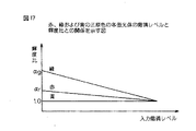
図17は赤、緑および青の三原色の各蛍光体の階調レベルと輝度比との関係を示す図であり、最大階調レベルにおける各色の輝度比を青色を基準として示すものである。また、図18は本発明に係るホワイトバランス補正回路の第6実施例を示すブロック図、図19は図18のホワイトバランス補正回路における赤、緑および青の三原色の各乗算係数を説明するための図、そして、図20は図18のホワイトバランス補正回路により補正された三原色の蛍光体の各階調レベルにおける輝度比を示す図である。 FIG. 17 is a diagram showing the relationship between the gradation level and the luminance ratio of the phosphors of the three primary colors of red, green and blue. The luminance ratio of each color at the maximum gradation level is shown with reference to blue. FIG. 18 is a block diagram showing a sixth embodiment of the white balance correction circuit according to the present invention. FIG. 19 is a diagram for explaining the multiplication factors of the three primary colors red, green and blue in the white balance correction circuit of FIG. FIG. 20 and FIG. 20 are diagrams showing luminance ratios at the respective gradation levels of the phosphors of the three primary colors corrected by the white balance correction circuit of FIG.
前述した図7〜図9と、図17,図19および図20との比較からも明らかなように、本第6実施例における三原色の蛍光体の各階調レベル(入力階調レベル)と輝度比αとの関係は、例えば、第1実施例における各発光回数と輝度比に対応させて考えることができる。 As is clear from comparison between FIGS. 7 to 9 and FIGS. 17, 19 and 20, the respective gradation levels (input gradation levels) and luminance ratios of the phosphors of the three primary colors in the sixth embodiment. The relationship with α can be considered, for example, corresponding to the number of times of light emission and the luminance ratio in the first embodiment.
図18において、参照符号11〜13は乗算器、2はマイコン、41〜43はγ補正回路、101は入力階調レベル検出部、102はアドレスデコーダ、103は記憶装置(ROM)、そして、141〜143は乗算器(出力階調レベル補正部)を示している。なお、乗算器11〜13、マイコン2およびγ補正回路41〜43は、前述した図4の従来例と同様のものであり、その説明は省略する。
In FIG. 18,
図18に示されるように、本第6実施例のホワイトバランス調整回路は、入力された映像信号R,G,Bにおける各入力階調レベルを入力階調レベル検出部101で検出(認識)し、それに従って、アドレスデコーダ102および記憶装置103を介して補正係数Lr,Lg,Lbを出力する。ここで、各補正係数Lは、L=1/αの関係、すなわち、Lr=1/αr,Lg=1/αg,Lb=1/αbの関係を有している。
As shown in FIG. 18, the white balance adjustment circuit of the sixth embodiment detects (recognizes) each input gradation level in the input video signals R, G, and B by the input gradation
各乗算器141,142(143)では、入力された補正係数Lr,Lg(Lb)により、以下の演算式に従った補正を行って出力階調レベルを算出する。ここで、Xを入力階調レベルとし、Yを出力階調レベルとし、βを最大入力階調レベルとする。
Each of the
Y(X)=L+(1−L)・(X/β)
なお、青色の映像信号を基準(規格化)とした場合には、Lb=1/αb=1/1=1となるため、青色の映像信号における入力階調レベルの補正は不要となり、従って、青色の映像信号用の乗算器143は設ける必要はない。
Y (X) = L + (1-L) · (X / β)
When the blue video signal is used as a standard (standardization), Lb = 1 / αb = 1/1 = 1, so that correction of the input gradation level in the blue video signal is unnecessary. It is not necessary to provide the
図18に示す第6実施例では、検出された入力階調レベルに応じた補正係数Lを記憶装置103から出力するように構成してあるが、例えば、マイコンを使用して入力階調レベルに応じた補正係数Lを演算し、それを各乗算器(出力階調レベル補正部)141〜143に供給するように構成してもよい。さらに、前述した各映像信号の振幅を発光回数または強度に従って調整して行うホワイトバランスの補正と兼用のマイコン等を使用してホワイトバランス補正回路を構成することもできる。
In the sixth embodiment shown in FIG. 18, the correction coefficient L corresponding to the detected input gradation level is output from the
図21は本発明に係るホワイトバランス補正回路の第6実施例の適用の有無による三原色の蛍光体の輝度特性を示す図である。 FIG. 21 is a diagram showing luminance characteristics of phosphors of three primary colors depending on whether or not the sixth embodiment of the white balance correction circuit according to the present invention is applied.
図21から明らかなように、本第6実施例のホワイトバランス補正回路を適用することにより、例えば、赤、緑および青の蛍光体の各階調レベルによるホワイトバランスの変化を、輝度比を一定に保つように調整することで、階調レベルに関わりなくホワイトバランスを維持することが可能になる。 As is apparent from FIG. 21, by applying the white balance correction circuit of the sixth embodiment, for example, the change in white balance due to the respective gradation levels of the phosphors of red, green and blue can be made constant in the luminance ratio. By adjusting so as to maintain the white balance, the white balance can be maintained regardless of the gradation level.
以上において、本発明の各実施の形態をプラズマディスプレイ装置を例にとって説明してきたが、例えば、赤、緑および青間で残光特性が異なる発光体を用いたカラー表示装置(例えば、CRT、LEDディスプレイ等)においても、発光回数を発光輝度(強度)と置き換えれば、本発明をそのまま適用してホワイトバランスを補正することが可能である。 In the above, each embodiment of the present invention has been described by taking a plasma display device as an example. For example, a color display device (for example, CRT, LED, etc.) using a light emitter having different afterglow characteristics among red, green, and blue. Also in a display or the like, if the number of times of light emission is replaced with light emission luminance (intensity), it is possible to correct the white balance by applying the present invention as it is.
[付記] 本発明は以下の特徴を有する。
(付記1) 入力された複数の原色映像信号に対応して発光回数または強度を制御してカラー表示を行う表示装置であって、
前記発光回数または強度を検出する手段と、
該検出された発光回数または強度に従って前記複数の原色映像信号の振幅を調整してホワイトバランスを補正する手段と、を備えたことを特徴とする表示装置。
[Appendix] The present invention has the following features.
(Supplementary Note 1) A display device that performs color display by controlling the number of times or intensity of light emission corresponding to a plurality of primary color video signals input,
Means for detecting the number or intensity of light emission;
A display device comprising: means for adjusting white balance by adjusting amplitudes of the plurality of primary color video signals according to the detected number of times of light emission or intensity.
(付記2) 付記1に記載の表示装置において、前記発光回数または強度を検出する手段は、前記複数の原色映像信号による画像の表示率から前記発光回数または強度を検出することを特徴とする表示装置。
(Supplementary note 2) In the display device according to
(付記3) 付記2に記載の表示装置において、該表示装置は、さらに、前記画像の表示率に従って前記複数の原色映像信号の発光回数または強度を制御する手段を備えたことを特徴とする表示装置。
(Supplementary note 3) The display device according to
(付記4) 付記3に記載の表示装置において、前記ホワイトバランスを補正する手段は演算手段および複数の乗算手段を備え、該演算手段は前記複数の原色映像信号の振幅係数を前記画像の表示率に従って演算し、該各乗算手段は該演算された振幅係数を前記各原色映像信号に乗算することを特徴とする表示装置。
(Supplementary note 4) In the display device according to
(付記5) 付記3に記載の表示装置において、前記ホワイトバランスを補正する手段は記憶手段および複数の乗算手段を備え、該記憶手段は前記複数の原色映像信号の振幅係数を前記画像の表示率に従って出力し、該各乗算手段は該記憶手段から出力された振幅係数を前記各原色映像信号に乗算することを特徴とする表示装置。
(Supplementary note 5) In the display device according to
(付記6) 付記3に記載の表示装置において、前記ホワイトバランスを補正する手段は記憶手段を備え、該記憶手段は前記各調整された振幅の原色映像信号を前記複数の原色映像信号と前記画像の表示率に従って出力することを特徴とする表示装置。
(Supplementary note 6) In the display device according to
(付記7) 付記1に記載の表示装置において、前記発光回数または強度を検出する手段は、前記複数の原色映像信号による画像表示時の表示電流から前記発光回数または強度を検出することを特徴とする表示装置。
(Supplementary note 7) In the display device according to
(付記8) 付記7に記載の表示装置において、該表示装置は、さらに、前記画像表示時の表示電流に従って前記複数の原色映像信号の発光回数または強度を制御する手段を備えたことを特徴とする表示装置。 (Supplementary note 8) In the display device according to supplementary note 7, the display device further includes means for controlling the number of light emission times or the intensity of the plurality of primary color video signals according to the display current at the time of the image display. Display device.
(付記9) 付記8に記載の表示装置において、前記ホワイトバランスを補正する手段は演算手段および複数の乗算手段を備え、該演算手段は前記複数の原色映像信号の振幅係数を前記画像表示時の表示電流に従って演算し、該各乗算手段は該演算された振幅係数を前記各原色映像信号に乗算することを特徴とする表示装置。 (Supplementary note 9) In the display device according to supplementary note 8, the means for correcting the white balance includes a calculation unit and a plurality of multiplication units, and the calculation unit calculates amplitude coefficients of the plurality of primary color video signals when the image is displayed. A display device that calculates in accordance with a display current, and wherein each of the multiplying means multiplies each of the primary color video signals by the calculated amplitude coefficient.
(付記10) 付記8に記載の表示装置において、前記ホワイトバランスを補正する手段は記憶手段および複数の乗算手段を備え、該記憶手段は前記複数の原色映像信号の振幅係数を前記画像表示時の表示電流に従って出力し、該各乗算手段は該記憶手段から出力された振幅係数を前記各原色映像信号に乗算することを特徴とする表示装置。 (Supplementary Note 10) In the display device according to supplementary note 8, the means for correcting the white balance includes a storage unit and a plurality of multiplication units, and the storage unit calculates amplitude coefficients of the plurality of primary color video signals at the time of image display. A display device that outputs in accordance with a display current, and wherein each multiplication means multiplies each primary color video signal by the amplitude coefficient outputted from the storage means.
(付記11) 付記8に記載の表示装置において、前記ホワイトバランスを補正する手段は記憶手段を備え、該記憶手段は前記各調整された振幅の原色映像信号を前記複数の原色映像信号と前記画像表示時の表示電流に従って出力することを特徴とする表示装置。 (Supplementary Note 11) In the display device according to supplementary note 8, the means for correcting the white balance includes a storage unit, and the storage unit converts the primary color video signals having the adjusted amplitudes to the plurality of primary color video signals and the image. A display device that outputs in accordance with a display current at the time of display.
(付記12) 付記1に記載の表示装置において、前記発光回数または強度を検出する手段は、外部からの輝度調整入力から前記発光回数または強度を検出することを特徴とする表示装置。
(Additional remark 12) The display apparatus of
(付記13) 付記12に記載の表示装置において、該表示装置は、さらに、前記外部からの輝度調整入力に従って前記複数の原色映像信号の発光回数または強度を制御する手段を備えたことを特徴とする表示装置。
(Supplementary note 13) In the display device according to
(付記14) 付記13に記載の表示装置において、前記ホワイトバランスを補正する手段は演算手段および複数の乗算手段を備え、該演算手段は前記複数の原色映像信号の振幅係数を前記外部からの輝度調整入力に従って演算し、該各乗算手段は該演算された振幅係数を前記各原色映像信号に乗算することを特徴とする表示装置。
(Supplementary note 14) In the display device according to
(付記15) 付記13に記載の表示装置において、前記ホワイトバランスを補正する手段は記憶手段および複数の乗算手段を備え、該記憶手段は前記複数の原色映像信号の振幅係数を前記外部からの輝度調整入力に従って出力し、該各乗算手段は該記憶手段から出力された振幅係数を前記各原色映像信号に乗算することを特徴とする表示装置。
(Supplementary note 15) In the display device according to
(付記16) 付記13に記載の表示装置において、前記ホワイトバランスを補正する手段は記憶手段を備え、該記憶手段は前記各調整された振幅の原色映像信号を前記複数の原色映像信号と前記外部からの輝度調整入力に従って出力することを特徴とする表示装置。
(Supplementary Note 16) In the display device according to
(付記17) 入力された複数の原色映像信号に対応して発光回数または強度を制御してカラー表示を行う表示装置であって、
前記複数の原色映像信号による画像の入力階調レベルに応じて当該複数の原色映像信号による画像の出力階調レベルを調整し、該複数の原色映像信号の発光回数または強度により変動するホワイトバランスを補正することを特徴とする表示装置。
(Supplementary Note 17) A display device that performs color display by controlling the number of times or intensity of light emission corresponding to a plurality of input primary color video signals,
The output gradation level of the image by the plurality of primary color video signals is adjusted according to the input gradation level of the image by the plurality of primary color video signals, and the white balance that varies depending on the number of times of emission or the intensity of the plurality of primary color video signals is adjusted. A display device characterized by correcting.
(付記18) 付記17に記載の表示装置において、該表示装置は、
前記複数の原色映像信号による画像の入力階調レベルを検出する手段と、
該検出された入力階調レベルに従って前記複数の原色映像信号の出力階調レベルを調整してホワイトバランスを補正する手段と、を備えたことを特徴とする表示装置。
(Supplementary note 18) In the display device according to
Means for detecting an input gradation level of an image by the plurality of primary color video signals;
And a means for adjusting white balance by adjusting output gradation levels of the plurality of primary color video signals in accordance with the detected input gradation level.
(付記19) 付記18に記載の表示装置において、前記ホワイトバランスを補正する手段は演算手段および複数の補正手段を備え、該演算手段は階調レベルの補正係数を前記検出された入力階調レベルに従って演算し、該各補正手段は該演算された補正係数を使用して入力階調レベルを補正処理することを特徴とする表示装置。
(Supplementary note 19) In the display device according to
(付記20) 付記18に記載の表示装置において、前記ホワイトバランスを補正する手段は記憶手段および複数の補正手段を備え、該記憶手段は階調レベルの補正係数を前記検出された入力階調レベルに従って出力し、該各補正手段は該出力された補正係数を使用して入力階調レベルを補正処理することを特徴とする表示装置。
(Supplementary note 20) In the display device according to
(付記21) 付記18〜20のいずれか1項に記載の表示装置において、該表示装置は、さらに、
前記複数の原色映像信号による画像の表示率或いは表示電流を検出する手段と、
該検出された表示率或いは表示電流に従って前記複数の原色映像信号の発光回数または強度を制御する手段と、を備えたことを特徴とする表示装置。
(Appendix 21) In the display device according to any one of
Means for detecting a display rate or display current of an image by the plurality of primary color video signals;
And a means for controlling the number of times or the intensity of light emission of the plurality of primary color video signals according to the detected display rate or display current.
(付記22) 付記1〜21のいずれか1項に記載の表示装置において、前記複数の原色映像信号による発光は、赤、緑および青の三原色蛍光体であることを特徴とする表示装置。
(Supplementary note 22) The display device according to any one of
(付記23) 付記1〜21のいずれか1項に記載の表示装置において、該表示装置は、プラズマディスプレイ装置であることを特徴とする表示装置。
(Supplementary note 23) The display device according to any one of
(付記24) 入力された複数の原色映像信号に対応して発光回数または強度を制御してカラー表示を行い、該発光回数または強度を検出する手段を備えた表示装置におけるホワイトバランス補正回路であって、
前記検出された発光回数または強度に従って前記複数の原色映像信号の振幅を調整してホワイトバランスを補正することを特徴とするホワイトバランス補正回路。
(Supplementary Note 24) A white balance correction circuit in a display device provided with means for performing color display by controlling the number of times of light emission or intensity corresponding to a plurality of input primary color video signals and detecting the number of times of light emission or intensity. And
A white balance correction circuit, wherein the white balance is corrected by adjusting amplitudes of the plurality of primary color video signals according to the detected number of times of light emission or intensity.
(付記25) 付記24に記載のホワイトバランス補正回路において、該ホワイトバランス補正回路は、
前記複数の原色映像信号の振幅係数を前記発光回数または強度に従って演算する演算手段と、
該演算された振幅係数を前記各原色映像信号に乗算する複数の乗算手段と、を備え、前記複数の原色映像信号の振幅を前記制御された発光回数または強度に従って調整し、該複数の原色映像信号の発光回数または強度により変動するホワイトバランスを補正するようにしたことを特徴とするホワイトバランス補正回路。
(Supplementary Note 25) In the white balance correction circuit according to Supplementary Note 24, the white balance correction circuit includes:
A calculation means for calculating an amplitude coefficient of the plurality of primary color video signals according to the number of emission times or the intensity;
A plurality of multiplication means for multiplying each primary color video signal by the calculated amplitude coefficient, and adjusting the amplitudes of the plurality of primary color video signals according to the controlled number of times of light emission or intensity; A white balance correction circuit which corrects a white balance which fluctuates according to the number of times or intensity of signal emission.
(付記26) 付記24に記載のホワイトバランス補正回路において、該ホワイトバランス補正回路は、
前記複数の原色映像信号の振幅係数を記憶し、前記発光回数または強度に従って出力する記憶手段と、
該演算された振幅係数を前記各原色映像信号に乗算する複数の乗算手段と、を備え、前記複数の原色映像信号の振幅を前記制御された発光回数または強度に従って調整し、該複数の原色映像信号の発光回数または強度により変動するホワイトバランスを補正するようにしたことを特徴とするホワイトバランス補正回路。
(Supplementary Note 26) In the white balance correction circuit according to Supplementary Note 24, the white balance correction circuit includes:
Storage means for storing amplitude coefficients of the plurality of primary color video signals, and outputting according to the number of times of light emission or intensity;
A plurality of multiplication means for multiplying each primary color video signal by the calculated amplitude coefficient, and adjusting the amplitudes of the plurality of primary color video signals according to the controlled number of times of light emission or intensity; A white balance correction circuit which corrects a white balance which fluctuates according to the number of times or intensity of signal emission.
(付記27) 付記24に記載のホワイトバランス補正回路において、該ホワイトバランス補正回路は、
前記各調整された振幅の原色映像信号を記憶し、前記複数の原色映像信号と前記発光回数または強度に従って出力する手段を備え、前記複数の原色映像信号の振幅を前記制御された発光回数または強度に従って調整し、該複数の原色映像信号の発光回数または強度により変動するホワイトバランスを補正するようにしたことを特徴とするホワイトバランス補正回路。
(Supplementary note 27) In the white balance correction circuit according to supplementary note 24, the white balance correction circuit includes:
Means for storing the adjusted primary color video signals according to the plurality of primary color video signals and the number of times or intensity of light emission, and controlling the amplitude of the plurality of primary color video signals as the controlled number of times of light emission or intensity. A white balance correction circuit that adjusts according to the above and corrects the white balance that fluctuates depending on the light emission frequency or intensity of the plurality of primary color video signals.
(付記28) 付記24に記載のホワイトバランス補正回路において、該ホワイトバランス補正回路は、
前記各調整された振幅の原色映像信号を記憶し、前記複数の原色映像信号と前記発光回数または強度に従って出力する手段を備え、前記複数の原色映像信号の振幅を前記制御された発光回数または強度に従って調整し、該複数の原色映像信号の発光回数または強度により変動するホワイトバランスを補正するようにしたことを特徴とするホワイトバランス補正回路。
(Supplementary note 28) In the white balance correction circuit according to supplementary note 24, the white balance correction circuit includes:
Means for storing the adjusted primary color video signals according to the plurality of primary color video signals and the number of times or intensity of light emission, and controlling the amplitude of the plurality of primary color video signals as the controlled number of times of light emission or intensity. A white balance correction circuit that adjusts according to the above and corrects the white balance that fluctuates depending on the light emission frequency or intensity of the plurality of primary color video signals.
(付記29) 付記24〜28のいずれか1項に記載のホワイトバランス補正回路において、前記発光回数または強度を検出する手段は、前記複数の原色映像信号による画像の表示率から前記発光回数または強度を検出することを特徴とするホワイトバランス補正回路。 (Supplementary note 29) In the white balance correction circuit according to any one of supplementary notes 24 to 28, the means for detecting the number of times of light emission or the intensity may include the number of times of light emission or the intensity based on an image display rate of the plurality of primary color video signals. A white balance correction circuit characterized by detecting an error.
(付記30) 付記24〜28のいずれか1項に記載のホワイトバランス補正回路において、前記発光回数または強度を検出する手段は、前記複数の原色映像信号による画像表示時の表示電流から前記発光回数または強度を検出することを特徴とするホワイトバランス補正回路。 (Supplementary Note 30) In the white balance correction circuit according to any one of Supplementary Notes 24 to 28, the means for detecting the number of times of light emission or the intensity is based on a display current at the time of image display by the plurality of primary color video signals. Alternatively, a white balance correction circuit that detects intensity.
(付記31) 付記24〜28のいずれか1項に記載のホワイトバランス補正回路において、前記発光回数または強度を検出する手段は、外部からの輝度調整入力から前記発光回数または強度を検出することを特徴とするホワイトバランス補正回路。 (Supplementary Note 31) In the white balance correction circuit according to any one of Supplementary Notes 24 to 28, the means for detecting the number of times of light emission or the intensity may detect the number of times of light emission or the intensity from an external luminance adjustment input. Characteristic white balance correction circuit.
(付記32) 付記24〜28のいずれか1項に記載のホワイトバランス補正回路において、該ホワイトバランス補正回路は、
前記複数の原色映像信号の振幅係数を前記発光回数または強度に従って演算する演算手段と、
該演算された振幅係数を前記各原色映像信号に乗算する複数の乗算手段と、を備え、前記複数の原色映像信号の振幅を前記制御された発光回数または強度に従って調整し、該複数の原色映像信号の発光回数または強度により変動するホワイトバランスを補正するようにしたことを特徴とするホワイトバランス補正回路。
(Supplementary Note 32) In the white balance correction circuit according to any one of Supplementary Notes 24 to 28, the white balance correction circuit includes:
A calculation means for calculating an amplitude coefficient of the plurality of primary color video signals according to the number of emission times or the intensity;
A plurality of multiplication means for multiplying each primary color video signal by the calculated amplitude coefficient, and adjusting the amplitudes of the plurality of primary color video signals according to the controlled number of times of light emission or intensity; A white balance correction circuit which corrects a white balance which fluctuates according to the number of times or intensity of signal emission.
(付記33) 入力された複数の原色映像信号に対応して発光回数または強度を制御してカラー表示を行い、該発光回数または強度を検出する手段を備えた表示装置におけるホワイトバランス補正回路であって、
前記複数の原色映像信号による画像の入力階調レベルに応じて当該複数の原色映像信号による画像の出力階調レベルを調整し、該複数の原色映像信号の発光回数または強度により変動するホワイトバランスを補正することを特徴とするホワイトバランス補正回路。
(Supplementary Note 33) A white balance correction circuit in a display device having means for controlling the number of times or intensity of light emission corresponding to a plurality of input primary color video signals to perform color display and detecting the number of times or intensity of light emission. And
The output gradation level of the image by the plurality of primary color video signals is adjusted according to the input gradation level of the image by the plurality of primary color video signals, and the white balance that varies depending on the number of times of emission or the intensity of the plurality of primary color video signals is adjusted. A white balance correction circuit characterized by correcting.
(付記34) 付記33に記載のホワイトバランス補正回路において、該ホワイトバランス補正回路は、
前記複数の原色映像信号による画像の入力階調レベルを検出する手段と、
該検出された入力階調レベルに従って前記複数の原色映像信号の出力階調レベルを調整してホワイトバランスを補正する手段と、を備えたことを特徴とするホワイトバランス補正回路。
(Supplementary Note 34) In the white balance correction circuit according to
Means for detecting an input gradation level of an image by the plurality of primary color video signals;
Means for adjusting white balance by adjusting output gradation levels of the plurality of primary color video signals in accordance with the detected input gradation level.
(付記35) 付記34に記載のホワイトバランス補正回路において、該ホワイトバランス補正回路は、
階調レベルの補正係数を前記検出された入力階調レベルに従って演算する演算手段と、
該演算された補正係数を使用して入力階調レベルを補正処理する複数の補正手段を備えたことを特徴とするホワイトバランス補正回路。
(Supplementary Note 35) In the white balance correction circuit according to
A calculation means for calculating a correction coefficient of a gradation level according to the detected input gradation level;
A white balance correction circuit comprising a plurality of correction means for correcting an input gradation level using the calculated correction coefficient.
(付記36) 付記34に記載のホワイトバランス補正回路において、該ホワイトバランス補正回路は、
階調レベルの補正係数を前記検出された入力階調レベルに従って出力する記憶手段と、
該出力された補正係数を使用して入力階調レベルを補正処理する複数の補正手段を備えたことを特徴とするホワイトバランス補正回路。
(Supplementary Note 36) In the white balance correction circuit according to
Storage means for outputting a gradation level correction coefficient in accordance with the detected input gradation level;
A white balance correction circuit comprising a plurality of correction means for correcting an input gradation level using the output correction coefficient.
(付記37) 付記34〜36のいずれか1項に記載のホワイトバランス補正回路において、該ホワイトバランス補正回路は、さらに、
前記複数の原色映像信号による画像の表示率或いは表示電流を検出する手段と、
該検出された表示率或いは表示電流に従って前記複数の原色映像信号の発光回数または強度を制御する手段と、を備えたことを特徴とするホワイトバランス補正回路。
(Supplementary note 37) In the white balance correction circuit according to any one of
Means for detecting a display rate or display current of an image by the plurality of primary color video signals;
A white balance correction circuit comprising: means for controlling the number of times of emission or intensity of the plurality of primary color video signals according to the detected display rate or display current.
(付記38) 付記24〜37のいずれか1項に記載のホワイトバランス補正回路において、前記複数の原色映像信号による発光は、赤、緑および青の三原色蛍光体であることを特徴とするホワイトバランス補正回路。 (Supplementary note 38) In the white balance correction circuit according to any one of supplementary notes 24 to 37, light emission by the plurality of primary color video signals is a red, green, and blue primary color phosphor. Correction circuit.
(付記39) 付記24〜37のいずれか1項に記載のホワイトバランス補正回路において、前記表示装置は、プラズマディスプレイ装置であることを特徴とするホワイトバランス補正回路。 (Supplementary note 39) The white balance correction circuit according to any one of supplementary notes 24 to 37, wherein the display device is a plasma display device.
(付記40) 入力された複数の原色映像信号に対応して輝度を制御してカラー表示を行う表示装置におけるホワイトバランス補正方法であって、
前記複数の原色映像信号の振幅比を前記原色映像信号の輝度に応じて設定し、該輝度によるホワイトバランスの変動を抑制するようにしたことを特徴とするホワイトバランス補正方法。
(Supplementary Note 40) A white balance correction method in a display device for performing color display by controlling luminance in response to a plurality of primary color video signals input,
A white balance correction method, wherein an amplitude ratio of the plurality of primary color video signals is set in accordance with a luminance of the primary color video signal, and a change in white balance due to the luminance is suppressed.
(付記41) 入力された複数の原色映像信号に対応して発光回数または強度を制御してカラー表示を行う表示装置におけるホワイトバランス補正方法であって、
前記発光回数または強度を検出し、
該検出された発光回数または強度に従って前記複数の原色映像信号の振幅を調整してホワイトバランスを補正するようにしたことを特徴とするホワイトバランス補正方法。
(Supplementary note 41) A white balance correction method in a display device for performing color display by controlling the number of times of light emission or intensity corresponding to a plurality of input primary color video signals,
Detecting the number of times or intensity of light emission;
A white balance correction method, wherein the white balance is corrected by adjusting the amplitudes of the plurality of primary color video signals according to the detected number of times of light emission or intensity.
(付記42) 付記41のホワイトバランス補正方法において、前記発光回数または強度の検出は、前記複数の原色映像信号による画像の表示率から求めるようになっていることを特徴とするホワイトバランス補正方法。
(Additional remark 42) The white balance correction method of
(付記43) 付記42のホワイトバランス補正方法において、該ホワイトバランス補正方法は、さらに、前記複数の原色映像信号の発光回数または強度を前記画像の表示率に従って制御するようになっていることを特徴とするホワイトバランス補正方法。
(Supplementary note 43) In the white balance correction method according to
(付記44) 付記41のホワイトバランス補正方法において、前記発光回数または強度の検出は、前記複数の原色映像信号による画像表示時の表示電流から求めるようになっていることを特徴とするホワイトバランス補正方法。
(Additional remark 44) The white balance correction method of
(付記45) 付記44のホワイトバランス補正方法において、該ホワイトバランス補正方法は、さらに、前記複数の原色映像信号の発光回数または強度を前記画像表示時の表示電流に従って制御するようになっていることを特徴とするホワイトバランス補正方法。 (Supplementary Note 45) In the white balance correction method of Supplementary Note 44, the white balance correction method further controls the number of times of emission or intensity of the plurality of primary color video signals according to the display current at the time of the image display. White balance correction method characterized by
(付記46) 付記41のホワイトバランス補正方法において、前記発光回数または強度の検出は、外部からの輝度調整入力から求めるようになっていることを特徴とするホワイトバランス補正方法。
(Additional remark 46) The white balance correction method of
(付記47) 付記46のホワイトバランス補正方法において、該ホワイトバランス補正方法は、さらに、前記複数の原色映像信号の発光回数または強度を前記外部からの輝度調整入力に従って制御するようになっていることを特徴とするホワイトバランス補正方法。 (Supplementary note 47) In the white balance correction method according to supplementary note 46, the white balance correction method further controls the number of times of emission or intensity of the plurality of primary color video signals in accordance with an external luminance adjustment input. White balance correction method characterized by
(付記48) 入力された複数の原色映像信号に対応して発光回数または強度を制御してカラー表示を行う表示装置におけるホワイトバランス補正方法であって、
前記複数の原色映像信号による画像の入力階調レベルに応じて当該複数の原色映像信号による画像の出力階調レベルを調整し、該複数の原色映像信号の発光回数または強度により変動するホワイトバランスを補正することを特徴とするホワイトバランス補正方法。
(Supplementary Note 48) A white balance correction method in a display device for performing color display by controlling the number of times or intensity of light emission corresponding to a plurality of primary color video signals input,
The output gradation level of the image by the plurality of primary color video signals is adjusted according to the input gradation level of the image by the plurality of primary color video signals, and the white balance that varies depending on the number of times of emission or the intensity of the plurality of primary color video signals is adjusted. A white balance correction method characterized by correcting.
(付記49) 付記48のホワイトバランス補正方法において、該ホワイトバランス補正方法は、
前記複数の原色映像信号による画像の入力階調レベルを検出し、
該検出された入力階調レベルに従って前記複数の原色映像信号の出力階調レベルを調整するようになっていることを特徴とするホワイトバランス補正方法。
(Supplementary Note 49) In the white balance correction method of Supplementary Note 48, the white balance correction method includes:
Detecting an input gradation level of an image by the plurality of primary color video signals;
2. A white balance correction method, wherein output gradation levels of the plurality of primary color video signals are adjusted according to the detected input gradation level.
(付記50) 付記48のホワイトバランス補正方法において、該ホワイトバランス補正方法は、さらに、前記複数の原色映像信号の発光回数または強度を前記画像の表示率或いは表示電流に従って制御するようになっていることを特徴とするホワイトバランス補正方法。 (Additional remark 50) In the white balance correction method according to additional remark 48, the white balance correction method further controls the number of times of emission or intensity of the plurality of primary color video signals according to the display rate or display current of the image. A white balance correction method characterized by the above.
(付記51) 入力された複数の原色映像信号に対応して輝度を制御してカラー表示を行う表示装置におけるホワイトバランス補正方法であって、
前記複数の原色映像信号の振幅比を前記原色映像信号の輝度に応じて設定し、該輝度によるホワイトバランスの変動を抑制するようにしたことを特徴とするホワイトバランス補正方法。
(Supplementary Note 51) A white balance correction method in a display device that performs color display by controlling luminance corresponding to a plurality of input primary color video signals,
A white balance correction method, wherein an amplitude ratio of the plurality of primary color video signals is set in accordance with a luminance of the primary color video signal, and a change in white balance due to the luminance is suppressed.
(付記52) 付記51に記載のホワイトバランス補正方法において、前記原色映像信号の輝度は、該原色映像信号の発光回数または強度により規定されることを特徴とするホワイトバランス補正方法。 (Supplementary note 52) The white balance correction method according to supplementary note 51, wherein the luminance of the primary color video signal is defined by the number of times of emission or intensity of the primary color video signal.
(付記53) 付記51または52に記載のホワイトバランス補正方法を適用し、前記複数の原色映像信号を発光体によってカラー表示するようにしたことを特徴とするホワイトバランス補正方法。 (Additional remark 53) The white balance correction method which applied the white balance correction method of Additional remark 51 or 52, and made it color-display the said several primary color video signal with a light-emitting body.
(付記54) 複数の原色映像信号を用いてカラー表示を行う表示装置におけるホワイトバランス補正回路であって、
前記各原色映像信号の振幅を調整する調整手段と、
前記複数の原色映像信号の振幅を補正するための信号振幅比を記憶する記憶手段と、
該記憶手段に記憶された信号振幅比を前記調整手段に設定する設定手段と、を備え、前記複数の原色映像信号の振幅比を該原色映像信号の発光回数または強度に応じて設定し、当該複数の原色映像信号の発光回数または強度により変動するホワイトバランスを補正するようにしたことを特徴とするホワイトバランス補正回路。
(Supplementary Note 54) A white balance correction circuit in a display device that performs color display using a plurality of primary color video signals,
Adjusting means for adjusting the amplitude of each primary color video signal;
Storage means for storing a signal amplitude ratio for correcting the amplitude of the plurality of primary color video signals;
Setting means for setting the signal amplitude ratio stored in the storage means in the adjustment means, and setting the amplitude ratio of the plurality of primary color video signals according to the number of times of emission or intensity of the primary color video signal, A white balance correction circuit which corrects white balance which fluctuates depending on the number of times or intensity of light emission of a plurality of primary color video signals.
(付記55) 複数の原色映像信号を用いてカラー表示を行う表示装置におけるホワイトバランス補正回路であって、
前記各原色映像信号の振幅を調整する調整手段と、
前記複数の原色映像信号の発光回数または強度から該各原色映像信号の振幅比を演算する演算手段と、
該演算手段から算出した振幅比を該調整手段に設定する設定手段と、を備え、前記複数の原色映像信号の振幅比を該原色映像信号の発光回数または強度に応じて設定し、当該複数の原色映像信号の発光回数または強度により変動するホワイトバランスを補正するようにしたことを特徴とするホワイトバランス補正回路。
(Supplementary Note 55) A white balance correction circuit in a display device that performs color display using a plurality of primary color video signals,
Adjusting means for adjusting the amplitude of each primary color video signal;
A computing means for computing an amplitude ratio of each primary color video signal from the number of times of emission or intensity of the plurality of primary color video signals;
Setting means for setting the amplitude ratio calculated from the calculation means in the adjustment means, and setting the amplitude ratio of the plurality of primary color video signals according to the number of times of emission or intensity of the primary color video signal, A white balance correction circuit which corrects a white balance which varies depending on the number of times or intensity of light emitted from a primary color video signal.
1:11,12,13 乗算器
2 マイクロコンピュータ
3 APL検出回路
31,33 加算器
32,34 レジスタ
4:41,42,43 ガンマ補正回路
5 電流検出回路
6 パネル駆動回路
7 発光回数制御回路
8;80;102 アドレスデコーダ
9;91,92,93;103 記憶装置(ROM)
10 表示パネル
11 アドレス電極
12 走査・維持電極
13 維持電極
14 アドレス駆動回路
15 走査・維持パルス出力回路
16 維持パルス出力回路
17 駆動制御回路
18 信号処理回路
101 入力階調レベル検出部
141〜143 出力階調レベル補正部
1:11, 12, 13
DESCRIPTION OF
Claims (3)
入力される前記複数の原色映像信号の表示率を検出し、
検出した前記表示率に応じて1フレームの発光回数を制御し、
前記表示率に応じた前記発光回数の制御により前記発光回数が第1の値から前記第1の値より大きい第2の値に変化した場合に、複数の蛍光体のうち輝度飽和特性の影響が最も小さい蛍光体に対応する原色映像信号の入力階調レベルに対する出力階調レベルの比の変化率を、他の蛍光体に対応する原色映像信号の入力階調レベルに対する出力階調レベルの比の変化率よりも相対的に小さくするように出力階調レベルを調整し、
調整した前記複数の原色映像信号の出力階調レベルに応じて、サブフィールド法により表示することを特徴とするプラズマディスプレイ装置の表示方法。 The gradation of the primary color video signal that is output according to the gradation level of the input primary color video signal in a plasma display device that receives a plurality of primary color video signals and performs color display by emitting phosphors of the primary colors A display method for changing the level and displaying the primary color video signal,
Detecting the display rate of the input primary color video signals;
Control the number of times of light emission per frame according to the detected display rate,
When the number of times of light emission is changed from a first value to a second value larger than the first value by controlling the number of times of light emission according to the display rate, the influence of luminance saturation characteristics among a plurality of phosphors is affected. The rate of change of the ratio of the output gradation level to the input gradation level of the primary color video signal corresponding to the smallest phosphor is determined by the ratio of the output gradation level to the input gradation level of the primary color video signal corresponding to the other phosphor. Adjust the output gradation level to be relatively smaller than the rate of change,
A display method for a plasma display device, wherein display is performed by a subfield method in accordance with the adjusted output gradation levels of the plurality of primary color video signals.
Priority Applications (1)
| Application Number | Priority Date | Filing Date | Title |
|---|---|---|---|
| JP2009073094A JP5262896B2 (en) | 2009-03-25 | 2009-03-25 | Display method of plasma display device |
Applications Claiming Priority (1)
| Application Number | Priority Date | Filing Date | Title |
|---|---|---|---|
| JP2009073094A JP5262896B2 (en) | 2009-03-25 | 2009-03-25 | Display method of plasma display device |
Related Parent Applications (1)
| Application Number | Title | Priority Date | Filing Date |
|---|---|---|---|
| JP2007023657A Division JP4310346B2 (en) | 2007-02-02 | 2007-02-02 | Display method of plasma display device |
Publications (2)
| Publication Number | Publication Date |
|---|---|
| JP2009134326A JP2009134326A (en) | 2009-06-18 |
| JP5262896B2 true JP5262896B2 (en) | 2013-08-14 |
Family
ID=40866181
Family Applications (1)
| Application Number | Title | Priority Date | Filing Date |
|---|---|---|---|
| JP2009073094A Expired - Fee Related JP5262896B2 (en) | 2009-03-25 | 2009-03-25 | Display method of plasma display device |
Country Status (1)
| Country | Link |
|---|---|
| JP (1) | JP5262896B2 (en) |
Families Citing this family (1)
| Publication number | Priority date | Publication date | Assignee | Title |
|---|---|---|---|---|
| JP6514482B2 (en) * | 2013-10-22 | 2019-05-15 | 株式会社ジャパンディスプレイ | Display device and color conversion method |
Family Cites Families (9)
| Publication number | Priority date | Publication date | Assignee | Title |
|---|---|---|---|---|
| JPH0851642A (en) * | 1994-08-08 | 1996-02-20 | Fujitsu General Ltd | White balance correction device |
| JP2720801B2 (en) * | 1994-10-27 | 1998-03-04 | 日本電気株式会社 | Plasma display panel driving method and plasma display panel driving device |
| JPH08223507A (en) * | 1995-02-20 | 1996-08-30 | Fujitsu General Ltd | Video signal amplitude limit circuit |
| JPH09281927A (en) * | 1996-04-19 | 1997-10-31 | Fujitsu General Ltd | Plasma display device |
| JPH1013848A (en) * | 1996-06-20 | 1998-01-16 | Fujitsu General Ltd | White balance adjustment system for plasma display panel |
| JPH1039829A (en) * | 1996-07-18 | 1998-02-13 | Fujitsu General Ltd | Compensation circuit for distortion of gradation of display device |
| JP3703247B2 (en) * | 1997-03-31 | 2005-10-05 | 三菱電機株式会社 | Plasma display apparatus and plasma display driving method |
| JP2000020013A (en) * | 1998-06-30 | 2000-01-21 | Fujitsu General Ltd | Video signal processing device |
| JP3580732B2 (en) * | 1999-06-30 | 2004-10-27 | 富士通株式会社 | Plasma display panel to keep color temperature or color deviation constant |
-
2009
- 2009-03-25 JP JP2009073094A patent/JP5262896B2/en not_active Expired - Fee Related
Also Published As
| Publication number | Publication date |
|---|---|
| JP2009134326A (en) | 2009-06-18 |
Similar Documents
| Publication | Publication Date | Title |
|---|---|---|
| JP3939066B2 (en) | Color plasma display device | |
| US7515119B2 (en) | Method and apparatus for calculating an average picture level and plasma display using the same | |
| JP2005122188A (en) | Driving apparatus for plasma display panel and gray level expression method thereof | |
| JP4160575B2 (en) | Plasma display device and driving method thereof | |
| JP2006163283A (en) | Plasma display device and method for controlling the same | |
| JP5262896B2 (en) | Display method of plasma display device | |
| JP4243238B2 (en) | Plasma display panel driving apparatus and gradation expression method thereof | |
| JP2007187909A (en) | Display apparatus | |
| JP4310346B2 (en) | Display method of plasma display device | |
| JP4268988B2 (en) | Display method of plasma display device | |
| JP2005128544A (en) | Method and system for decreasing afterimage of plasma display panel | |
| JP2006528791A (en) | Plasma display panel driving apparatus and method | |
| JP4653146B2 (en) | Plasma display device and control method thereof | |
| KR100489281B1 (en) | Method and Apparatus of Driving Plasma Display Panel | |
| KR100839378B1 (en) | Plasma display and driving method thereof | |
| JP2010033098A (en) | Plasma display and display method of the same | |
| JP2005140950A (en) | Color temperature change compensation method, image display method, and plasma display | |
| JP2010181907A (en) | Plasma display device and display method of the same | |
| KR20060083041A (en) | Plasma display panel driving device and method thereof | |
| JP2008052068A (en) | Plasma display device | |
| JP2013148800A (en) | Plasma display device | |
| JP2007133289A (en) | Plasma display device |
Legal Events
| Date | Code | Title | Description |
|---|---|---|---|
| A521 | Written amendment |
Free format text: JAPANESE INTERMEDIATE CODE: A523 Effective date: 20090325 |
|
| A621 | Written request for application examination |
Free format text: JAPANESE INTERMEDIATE CODE: A621 Effective date: 20090325 |
|
| A521 | Written amendment |
Free format text: JAPANESE INTERMEDIATE CODE: A523 Effective date: 20090325 |
|
| A711 | Notification of change in applicant |
Free format text: JAPANESE INTERMEDIATE CODE: A711 Effective date: 20120314 |
|
| A131 | Notification of reasons for refusal |
Free format text: JAPANESE INTERMEDIATE CODE: A131 Effective date: 20120612 |
|
| A521 | Written amendment |
Free format text: JAPANESE INTERMEDIATE CODE: A523 Effective date: 20120807 |
|
| A131 | Notification of reasons for refusal |
Free format text: JAPANESE INTERMEDIATE CODE: A131 Effective date: 20130108 |
|
| A521 | Written amendment |
Free format text: JAPANESE INTERMEDIATE CODE: A523 Effective date: 20130307 |
|
| TRDD | Decision of grant or rejection written | ||
| A01 | Written decision to grant a patent or to grant a registration (utility model) |
Free format text: JAPANESE INTERMEDIATE CODE: A01 Effective date: 20130402 |
|
| A61 | First payment of annual fees (during grant procedure) |
Free format text: JAPANESE INTERMEDIATE CODE: A61 Effective date: 20130415 |
|
| S111 | Request for change of ownership or part of ownership |
Free format text: JAPANESE INTERMEDIATE CODE: R313111 |
|
| R350 | Written notification of registration of transfer |
Free format text: JAPANESE INTERMEDIATE CODE: R350 |
|
| S111 | Request for change of ownership or part of ownership |
Free format text: JAPANESE INTERMEDIATE CODE: R313111 |
|
| R350 | Written notification of registration of transfer |
Free format text: JAPANESE INTERMEDIATE CODE: R350 |
|
| LAPS | Cancellation because of no payment of annual fees |