JP5259382B2 - Semiconductor memory device - Google Patents
Semiconductor memory device Download PDFInfo
- Publication number
- JP5259382B2 JP5259382B2 JP2008333972A JP2008333972A JP5259382B2 JP 5259382 B2 JP5259382 B2 JP 5259382B2 JP 2008333972 A JP2008333972 A JP 2008333972A JP 2008333972 A JP2008333972 A JP 2008333972A JP 5259382 B2 JP5259382 B2 JP 5259382B2
- Authority
- JP
- Japan
- Prior art keywords
- replica
- circuit
- input
- gate
- timing
- Prior art date
- Legal status (The legal status is an assumption and is not a legal conclusion. Google has not performed a legal analysis and makes no representation as to the accuracy of the status listed.)
- Expired - Fee Related
Links
Images


Classifications
-
- G—PHYSICS
- G11—INFORMATION STORAGE
- G11C—STATIC STORES
- G11C7/00—Arrangements for writing information into, or reading information out from, a digital store
- G11C7/22—Read-write [R-W] timing or clocking circuits; Read-write [R-W] control signal generators or management
-
- G—PHYSICS
- G11—INFORMATION STORAGE
- G11C—STATIC STORES
- G11C7/00—Arrangements for writing information into, or reading information out from, a digital store
- G11C7/02—Arrangements for writing information into, or reading information out from, a digital store with means for avoiding parasitic signals
-
- G—PHYSICS
- G11—INFORMATION STORAGE
- G11C—STATIC STORES
- G11C7/00—Arrangements for writing information into, or reading information out from, a digital store
- G11C7/22—Read-write [R-W] timing or clocking circuits; Read-write [R-W] control signal generators or management
- G11C7/227—Timing of memory operations based on dummy memory elements or replica circuits
Landscapes
- Dram (AREA)
- Static Random-Access Memory (AREA)
Description
本発明は、半導体記憶装置に関し、特に、センスアンプ回路の活性化タイミングの生成に関する。 The present invention relates to a semiconductor memory device, and more particularly to generation of activation timing of a sense amplifier circuit.
一般的な半導体記憶装置において、データ読み出しは、メモリセルの保持するデータに応じてビット線にあらわれた信号レベルが、センスアンプ回路で検知・増幅された上で、外部に出力されることで実現されている。 In a general semiconductor memory device, data reading is realized by the signal level appearing on the bit line corresponding to the data held in the memory cell being detected and amplified by the sense amplifier circuit and then output to the outside. Has been.
したがって、半導体記憶装置の動作周期を早くするには、メモリセルの選択からセンスアンプ回路の活性化までの時間を短縮することが有効である。 Therefore, to shorten the operation cycle of the semiconductor memory device, it is effective to shorten the time from selection of the memory cell to activation of the sense amplifier circuit.
しかし、センスアンプ回路を早く活性化させると、ビット線に十分な信号レベルが現れる前のデータを検知・増幅することになる。この場合、誤読み出しの原因となる。 However, when the sense amplifier circuit is activated early, data before a sufficient signal level appears on the bit line is detected and amplified. In this case, erroneous reading may be caused.
そこで、適切なセンスアンプ回路の活性化タイミングを生成する技術として、レプリカ回路を用いるものがある(特許文献1)。このレプリカ回路は、メモリセルアレイと同等の構造を持つものであり、メモリセルからのデータ読み出しのタイミングをレプリカ回路で模擬した上で、そのタイミングによりセンスアンプ回路を活性化させるというものである。 Therefore, as a technique for generating an appropriate activation timing of the sense amplifier circuit, there is a technique using a replica circuit (Patent Document 1). This replica circuit has a structure equivalent to that of a memory cell array, and simulates the timing of data reading from the memory cell by the replica circuit and activates the sense amplifier circuit at that timing.
しかし、通常、レプリカ回路が生成したタイミングは、いくつかの回路を通過し、センスアンプ回路に与えられる。そのため、それら回路によって生じる遅延時間の影響から、レプリカ回路は、十分にメモリセルアレイを模擬しているとは言えない。 However, the timing generated by the replica circuit usually passes through several circuits and is given to the sense amplifier circuit. Therefore, it cannot be said that the replica circuit sufficiently simulates the memory cell array due to the influence of the delay time caused by these circuits.
また、温度等により生じるメモリセルの特性の変化を、レプリカ回路によって再現することができるものの、前述した回路については、この変化を反映することができないため問題となる。
本発明は、レプリカ遅延時間を量子化し、その結果に基づいて最適なセンスアンプ回路の活性化タイミングを生成する半導体記憶装置を提供することを目的とする。 An object of the present invention is to provide a semiconductor memory device that quantizes a replica delay time and generates an optimum activation timing of a sense amplifier circuit based on the result.
本発明の一つの態様において、半導体記憶装置は、複数のワード線、前記ワード線に交差する複数のビット線、前記ワード線及び前記ビット線の各交差部に設けられた複数のメモリセルからなるメモリセルアレイと、前記ビット線の信号レベルを検知・増幅する複数のセンスアンプ回路と、レプリカワード線、前記レプリカワード線に交差するレプリカビット線、前記レプリカワード線及びレプリカビット線の各交差部に設けられたレプリカメモリセルからなり、前記メモリセルの読み出し動作を模擬するレプリカ回路と、基準タイミングから前記レプリカビット線が変化するまでの時間であるレプリカ遅延時間を量子化し、その結果に基づいて、前記センスアンプ回路の活性化タイミングを生成するタイミング発生回路とを有することを特徴とする。 In one embodiment of the present invention, a semiconductor memory device includes a plurality of word lines, a plurality of bit lines intersecting the word lines, and a plurality of memory cells provided at each intersection of the word lines and the bit lines. A memory cell array, a plurality of sense amplifier circuits that detect and amplify the signal level of the bit line, a replica word line, a replica bit line that intersects the replica word line, and each intersection of the replica word line and replica bit line A replica circuit composed of a provided replica memory cell, and a replica circuit that simulates a read operation of the memory cell, and a replica delay time that is a time from a reference timing until the replica bit line changes, and based on the result, And a timing generation circuit for generating an activation timing of the sense amplifier circuit. To.
本発明によれば、レプリカ遅延時間を量子化し、その結果に基づいて最適なセンスアンプ回路の活性化タイミングを生成する半導体記憶装置を提供することができる。 According to the present invention, it is possible to provide a semiconductor memory device that quantizes a replica delay time and generates an optimum activation timing of a sense amplifier circuit based on the result.
以下、図面を参照しながら、本発明に係る半導体記憶装置の実施の形態について詳細に説明する。 Hereinafter, embodiments of a semiconductor memory device according to the present invention will be described in detail with reference to the drawings.
[第1の実施形態]
図1は、本発明の第1の実施形態に係る半導体記憶装置の概略図である。
[First Embodiment]
FIG. 1 is a schematic diagram of a semiconductor memory device according to the first embodiment of the present invention.
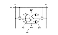
この半導体記憶装置は、複数のワード線WL、これら複数のワード線WLに交差する相補対のビット線BL、/BLからなるビット線対、及びワード線WL及びビット線対の各交差部に接続された複数のメモリセルからなるメモリセルアレイを備える。ここで、ビット線BLが持つ寄生容量をCとする。 The semiconductor memory device is connected to a plurality of word lines WL, complementary bit lines BL crossing the plurality of word lines WL, bit line pairs consisting of / BL, and each intersection of the word lines WL and bit line pairs. A memory cell array including a plurality of memory cells. Here, let C be the parasitic capacitance of the bit line BL.
また、各ビット線対の端部に、ビット線BL、/BLに現れる微小信号を検知・増幅するためのセンスアンプ回路SAを備える。 Further, a sense amplifier circuit SA for detecting and amplifying a minute signal appearing on the bit lines BL and / BL is provided at the end of each bit line pair.
さらに、ビット線BLと同じ寄生容量Cを持つレプリカビット線RBL、このレプリカビット線RBLに交差するレプリカワード線RWL、及びこれらレプリカビット線RBL、レプリカワード線RWLに接続され、メモリセルMCと同じ構造を持つレプリカセルRCからなるレプリカ回路を備える。 Further, the replica bit line RBL having the same parasitic capacitance C as the bit line BL, the replica word line RWL crossing the replica bit line RBL, and the replica bit line RBL and the replica word line RWL are connected to the same as the memory cell MC. A replica circuit including a replica cell RC having a structure is provided.
このレプリカ回路のレプリカビット線RBLの端部に、レプリカビット線に現れる微小信号を検知・増幅するためのインバータIV1を備える。また、2つの入力A及びBを備え、それぞれにレプリカワード線RWL及びインバータIV1の出力端が接続されたタイミング発生回路100を備える。ここで、入力Aに入力される信号を基準信号(基準タイミング)、入力Bに入力される信号をレプリカ遅延信号と呼ぶ。このレプリカ発生回路100は、基準信号及びレプリカ遅延信号に基づいてセンスアンプ回路SAを活性化させるためのセンスアンプ回路活性化信号SAENBLを発生させるものである。また、外部より与えられる複数ビットの選択信号SELに応じて、センスアンプ回路活性化信号SAENBLより所定時間タイミングが早いデジタル出力DOを得ることができる。
An inverter IV1 for detecting and amplifying a minute signal appearing on the replica bit line is provided at the end of the replica bit line RBL of the replica circuit. Further, it includes a
メモリセルMCは、例えば、図2に示すような6トランジスタ型メモリセルである。すなわち、6トランジスタ型メモリセルは、ソースが電源電圧Vddの電源線及び接地電圧Vssの接地線にそれぞれ接続され相補対接続されたPMOSトランジスタQ1及びNMOSトランジスタQ2を備えた第2のインバータIV2と、ソースが電源線及び接地線にそれぞれ接続され相補対接続されたPMOSトランジスタQ3及びNMOSトランジスタQ4を備えた第3のインバータIV3とを有する。これらインバータIV2,IV3の入力と出力は相互に接続されている。ビット線BLとインバータIV2の出力端との間には、トランスファトランジスタQ5が接続され、ビット線/BLとインバータIV3の出力端との間には、トランスファトランジスタQ6が接続されている。これらトランスファトランジスタQ5、Q6のゲートは、ワード線WLに接続されている。なお、この6トランジスタ型メモリセルを用いた書き込み動作は、ビット線BL及び/BLの双方で行われるが、読み出し動作については、一方のビット線BL又は/BLのみからなされるシングルエンド読み出しでも良い。 The memory cell MC is, for example, a 6-transistor type memory cell as shown in FIG. That is, the 6-transistor type memory cell includes a second inverter IV2 having a PMOS transistor Q1 and an NMOS transistor Q2 whose sources are connected to a power supply line of the power supply voltage Vdd and a ground line of the ground voltage Vss, respectively, and connected in a complementary pair. The source includes a third inverter IV3 including a PMOS transistor Q3 and an NMOS transistor Q4 connected to a power supply line and a ground line, respectively, and connected in a complementary pair. The inputs and outputs of these inverters IV2 and IV3 are connected to each other. A transfer transistor Q5 is connected between the bit line BL and the output terminal of the inverter IV2, and a transfer transistor Q6 is connected between the bit line / BL and the output terminal of the inverter IV3. The gates of these transfer transistors Q5 and Q6 are connected to the word line WL. Note that the write operation using the 6-transistor type memory cell is performed on both the bit lines BL and / BL, but the read operation may be a single-ended read performed only from one bit line BL or / BL. .
なお、以下の説明において、電源電圧Vddの信号レベルを“H”、接地電圧Vssの信号レベルを“L”と表現することもある。 In the following description, the signal level of the power supply voltage Vdd may be expressed as “H” and the signal level of the ground voltage Vss may be expressed as “L”.
次に、タイミング発生回路100について図3を用いて説明する。
Next, the
タイミング発生回路100は、往路回路100aと復路回路100bとを備える。
The
往路回路100aは、基準信号が入力されるインバータG101を備える。また、このインバータG101の出力端が入力端に接続されたNANDゲートG103、このNANDゲートG103の出力端が入力端に接続されたインバータG104を備え、以降、1個のNANDゲート及び1個のインバータからなる回路パターンの繰り返しになっている。ここで、NANDゲートG103、G106、G109、G112のもう一方の入力は“H”に固定されている。以下において、インバータG101、G104、G107、G110、・・・の出力端をそれぞれノードNA0、NA1、NA2、NA3、・・・と呼ぶ。また、各ノードNA間の構成を「ステージ」と呼ぶ。つまり、図3の場合、各ステージは、1個のNANDゲートと1個のインバータで構成されていることになる。さらに、往路回路100aは、一方の入力端にノードNA0、NA1、NA2、NA3、・・・がそれぞれ接続され、もう一方の入力に入力Bが共通に接続されたNANDゲートG102、G105、G108、G111を備える。
The
この往路回路100aは、基準信号の立ち上がりとレプリカ遅延信号の立ち上がりのタイミング差を量子化するものである。その結果は、NANDゲートG101、G105、G108、G111、・・・の出力として現れる。以下において、これらNANDゲートの出力をそれぞれノードNB0、NB1、NB2、NB3、・・・と呼ぶ。
The
復路回路100bは、インバータG113の出力が入力されるNANDゲートG115、このNANDゲートG115の出力端が入力端に接続されたインバータG116を備える。以降、往路回路100aと同様、1個のインバータ及び1個のNANDゲートからなる回路パターンが繰り返される。さらに、入力端の1つにインバータG122の出力端が接続されたNANDゲートG124を備える。このNANDゲートG124の出力がセンスアンプ回路活性化信号SAENBLとなる。ここで、NANDゲートG124、G121、G118、G115、・・・のもう一方の入力端には、それぞれ往路回路100aのNANDゲートG102、G105、G108、G111の出力端が接続されている。さらに、一方の入力端にそれぞれインバータG122、G119、G116、G113の出力端が接続されたNANDゲートG123、G120、G117、G114、・・・を備える。これらNANDゲートG123、G120、G117、G114、・・・のもう一方の入力端には、それぞれ選択信号SEL[0]、SEL[1]、SEL[2]、SEL[3]、・・・が入力される。これらNANDゲートG123、G120、G117、G114、・・・の出力が、それぞれデジタル出力DO[0]、DO[1]、DO[2]、DO[3]、・・・となる。なお、以下において、往路回路101aの場合と同様、インバータG122、G119、G116、G113、・・・の出力端をそれぞれノードNC0、NC1、NC2、NC3、・・・と呼び、各NC間の構成を「ステージ」と呼ぶ。
The
この復路回路100bは、ノードNBに現れた信号変化をノードNCを介してセンスアンプ回路活性化信号SAENBLとして出力するものである。
The
次に、以上の構成によるタイミング発生回路100の動作について説明する。
Next, the operation of the
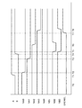
図3は、タイミング発生回路100の動作波形である。
FIG. 3 shows operation waveforms of the
データ読み出し前(時刻T0)において、レプリカワード線RWLは、ワード線WLとともに非選択状態である。したがって、入力Aに入力される基準信号は“L”である。一方、レプリカビット線RBLは、ビット線BL、/BL同様、“H”にプリチャージされている。したがって、インバータIV1の出力、つまり入力Bの信号は“L”となっている。ここで、ノードNA0、NA1、NA2、NA3、・・・は、全て“H”となっている。 Before data reading (time T0), the replica word line RWL is in a non-selected state together with the word line WL. Therefore, the reference signal input to the input A is “L”. On the other hand, the replica bit line RBL is precharged to “H” like the bit lines BL and / BL. Therefore, the output of the inverter IV1, that is, the signal of the input B is “L”. Here, the nodes NA0, NA1, NA2, NA3,... Are all “H”.
続いて、時刻T1において、所定のワード線WLが選択されるとともに、レプリカワード線RWLも選択される。したがって、基準信号は“H”になる。一方、レプリカビット線RBLには、レプリカセルRCのデータが流入し、徐々に“L”に低下していく。 Subsequently, at time T1, a predetermined word line WL is selected and a replica word line RWL is also selected. Therefore, the reference signal becomes “H”. On the other hand, data of the replica cell RC flows into the replica bit line RBL and gradually decreases to “L”.
続いて、時刻T2において、先の時刻T1で“L”から“H”に立ち上がった基準信号の影響により、ノードNA0は、“H”から“L”に立ち下がる。 Subsequently, at time T2, the node NA0 falls from “H” to “L” due to the influence of the reference signal that rises from “L” to “H” at the previous time T1.
続いて、時刻T3において、先の時刻T2で“L”から“H”に立ち上がったノードNA0の影響により、ノードNA1は、“H”から“L”に立ち下がる。ここで、ノードNA0の立ち下がり(時刻T1)からノードNB1の立ち下がり(時刻T2)までの時間は、ノードNA0及びNA1間のステージを構成するNANDゲートG103及びインバータG104で生じる遅延時間により決定する。以下において、ステージ毎の遅延時間を「ステップ時間」と呼ぶ。 Subsequently, at time T3, the node NA1 falls from “H” to “L” due to the influence of the node NA0 that rises from “L” to “H” at the previous time T2. Here, the time from the fall of the node NA0 (time T1) to the fall of the node NB1 (time T2) is determined by the delay time generated in the NAND gate G103 and the inverter G104 that constitute the stage between the nodes NA0 and NA1. . Hereinafter, the delay time for each stage is referred to as “step time”.
続いて、時刻T6において、先の時刻T3で“L”から“H”に立ち上がったノードNA1の影響により、ノードNA2は、“H”から“L”に立ち下がる。このときのステップ時間も、ノードNA0及びNA1間のステップ時間と同じである。 Subsequently, at time T6, the node NA2 falls from “H” to “L” due to the influence of the node NA1 that rises from “L” to “H” at the previous time T3. The step time at this time is also the same as the step time between the nodes NA0 and NA1.
続いて、時刻T8において、先の時刻T6で“L”から“H”に立ち上がったノードNA2の影響により、ノードNA3は、“H”から“L”に立ち下がる。このときのステップ時間も、ノードNA0及びNA1間のステップ時間と同じである。 Subsequently, at time T8, the node NA3 falls from “H” to “L” due to the influence of the node NA2 which rises from “L” to “H” at the previous time T6. The step time at this time is also the same as the step time between the nodes NA0 and NA1.
以降、先の時刻T2、T3、T6、及びT8と同様、1ステップ時間毎に順次ノードNAが“H”から“L”に立ち下がる。 Thereafter, like the previous times T2, T3, T6, and T8, the node NA sequentially falls from “H” to “L” for each step time.
一方、時刻T1から徐々に低下するレプリカビット線RBLのレベルが、インバータIV1の閾値以下になると、インバータIV3の出力、つまりレプリカ遅延信号が“L”から“H”に立ち上がる。このときの時刻を、ノートNA1及びNA2の信号が変化する時刻T3及びT6間の時刻T4とする。 On the other hand, when the level of the replica bit line RBL that gradually decreases from time T1 becomes equal to or lower than the threshold value of the inverter IV1, the output of the inverter IV3, that is, the replica delay signal rises from “L” to “H”. The time at this time is a time T4 between times T3 and T6 when the signals of the notes NA1 and NA2 change.
続いて、時刻T5において、時刻T4の時点で基準信号の立ちあがりの影響を受けていないノードNA2、NA3は“H”のままであるため、レプリカ遅延信号の立ち上がりをきっかけにノードNB2、NB3は、“L”に変化する。言い換えれば、基準電圧の立ち上がりが遅延を伴いながら順次ノードNA0、NA1、・・・に伝搬され、レプリカ遅延信号が立ち上がった時点で、まだ基準電圧の立ち上がりが伝搬されていない以後のノードNAとレプリカ遅延信号を入力とするNANDゲートの出力であるノードNBが“H”から“L”に立ち下がることになる。つまり、複数のノードNBは、レプリカワード線RWLの選択(基準信号の立ち上がり:時刻T1)からレプリカセルRCのデータがレプリカビット線RBLに十分に現れる(レプリカ遅延信号の立ち上がり:時刻T4)までの時間をステップ時間で量子化した結果となっている。 Subsequently, at time T5, the nodes NA2 and NA3 that are not affected by the rise of the reference signal at the time T4 remain “H”, so that the nodes NB2 and NB3 are triggered by the rise of the replica delay signal. Changes to “L”. In other words, the rising edge of the reference voltage is sequentially propagated to the nodes NA0, NA1,... With a delay, and when the replica delay signal rises, the node NA and the replica after which the rising edge of the reference voltage has not been propagated yet. The node NB, which is the output of the NAND gate that receives the delay signal, falls from “H” to “L”. That is, the plurality of nodes NB from the selection of the replica word line RWL (rising of the reference signal: time T1) until the data of the replica cell RC sufficiently appears on the replica bit line RBL (rising of the replica delay signal: time T4). It is the result of quantizing the time with the step time.
続いて、時刻T7において、センスアンプ回路活性化信号SAENBLは、“L”から“H”に立ち上がる。 Subsequently, at time T7, the sense amplifier circuit activation signal SAENBL rises from “L” to “H”.
ここで、時刻T5から時刻T7までの遅延時間は、“L”から“H”に立ち下がるノードNB2、NB3のうち、ノードNC0に最も近いノードNB2からノードNA0までのステージで生ずる遅延により決定する。往路回路100bのステージは、復路回路100aのステージと同じ構成となっているため、基準信号が立ち上がってからノードNA2が立ち下がるまでの時間と、ほぼ同じ遅延が生ずることになる。したがって、基準信号が立ち上がってからセンスアンプ回路活性化信号SAENBLが立ち上がるまでの時間は、基準電圧が立ち上がってからレプリカ遅延信号が立ち上がるまでの時間のほぼ2倍となる。言い換えれば、レプリカワード線RWLが選択されてからインバータIV1がレプリカビット線RBLの微小信号を検知するまでの時間のほぼ2倍のタイミングを生成したことになる。
Here, the delay time from the time T5 to the time T7 is determined by the delay generated in the stage from the node NB2 to the node NA0 closest to the node NC0 among the nodes NB2 and NB3 falling from “L” to “H”. . Since the stage of the
なお、復路回路100bが備えるNANDゲートG123、G120、・・・は、往路回路100aのNANDゲートG102、G105、・・・に相当するものである。これにより、往路回路100aのインバータG101、G104、・・・と復路回路100bのインバータG113、G116、・・・により駆動される負荷を同じにすることができる。また、複数のビットからなる選択信号SELの各ビット[0]、[1]、・・・はセンスノードNC0、NC1に対応しており、例えば、選択信号SEL[0]=“H”を与えることでセンスノードNC0の信号をNANDゲートG123を介して外部に出力させることができる。つまり、NANDゲートG123、G120、・・・があることで、センスアンプ回路活性化信号SAENBLの活性化タイミングよりも早いタイミングの信号をステップ単位で取り出すことができる。
Note that the NAND gates G123, G120,... Provided in the
ここで、データ読み出し時のセンスアンプ回路SAの活性化タイミングについて説明する。 Here, the activation timing of the sense amplifier circuit SA at the time of data reading will be described.
まず、半導体記憶装置の処理スピードの観点からすれば、ワード線WLを選択した後、できるだけ早くセンスアンプ回路SAを活性化させれば良い。しかし、“H”にプリチャージされたビット線BL、/BLが“L”に引き下がるまでには、ある程度の時間を要する。ここで、ビット線BLの容量をC、メモリセルMCに流入する電流をIc、メモリセルMCが選択されてからの時間をtとすると、ビット線BL、/BL間の電位差ΔVは、ΔV=(Ic/C)×tとなる。したがって、時間t又は電流Icが大きくなると電位差ΔVblを大きくなり、寄生容量Cが大きくなると、電位差ΔVblが小さくなる。実際、ビット線BL、/BLの電位差ΔVblを100mVとして寄生容量Cや電流Icを考慮すると、時間tは100m〜200ms程度となる。つまり、このタイミングでセンスアンプ回路SAを活性化させることが望ましい。ただし、寄生容量Cや電流Icは、温度などの環境変化によって変化するため、そそれに対する時間tの調整が必要となる。 First, from the viewpoint of the processing speed of the semiconductor memory device, the sense amplifier circuit SA may be activated as soon as possible after the word line WL is selected. However, a certain amount of time is required until the bit lines BL and / BL precharged to “H” are pulled down to “L”. Here, when the capacity of the bit line BL is C, the current flowing into the memory cell MC is Ic, and the time after the memory cell MC is selected is t, the potential difference ΔV between the bit lines BL and / BL is ΔV = (Ic / C) × t. Therefore, the potential difference ΔVbl increases as the time t or the current Ic increases, and the potential difference ΔVbl decreases as the parasitic capacitance C increases. Actually, when the potential difference ΔVbl between the bit lines BL and / BL is set to 100 mV and the parasitic capacitance C and the current Ic are taken into consideration, the time t is about 100 m to 200 ms. That is, it is desirable to activate the sense amplifier circuit SA at this timing. However, since the parasitic capacitance C and the current Ic change due to environmental changes such as temperature, it is necessary to adjust the time t accordingly.
そこで、一般的にレプリカ回路が使用される。この場合、メモリセルアレイとレプリカ回路とは同じ環境下にあるため、レプリカビット線RBLの信号が検知したタイミングでセンスアンプ回路活性化信号を活性化すれば、環境の変化に対応した最適なタイミングでセンスアンプ回路SAを活性化させてやることができるとも考えられる。 Therefore, a replica circuit is generally used. In this case, since the memory cell array and the replica circuit are in the same environment, if the sense amplifier circuit activation signal is activated at the timing when the signal of the replica bit line RBL is detected, the optimum timing corresponding to the environmental change is obtained. It can be considered that the sense amplifier circuit SA can be activated.
ただし、1個のレプリカセルRCだけでは、レプリカビット線RBLを“L”に引き下げる駆動力が小さいため、レプリカビット線RBLに十分な信号レベルが現れてからセンスアンプ回路SAを活性化させていたのでは処理が遅くなる。そこで、通常、レプリカセルRCは複数同時に選択される。これに伴い、レプリカビット線RBLが“L”に引き下げられるまでの時間が短くなるため、インバータ等のゲートによりタイミングを遅延させた上で、センスアンプ回路SAを活性化させることになる。 However, since only one replica cell RC has a small driving force to pull the replica bit line RBL to “L”, the sense amplifier circuit SA is activated after a sufficient signal level appears on the replica bit line RBL. Will slow down the process. Therefore, normally, a plurality of replica cells RC are selected simultaneously. Along with this, the time until the replica bit line RBL is pulled down to “L” is shortened, so that the sense amplifier circuit SA is activated after the timing is delayed by the gate of an inverter or the like.
ここで、レプリカセルRCの個数をnとすると、レプリカビット線RBLに電源電圧Vddとの電位差ΔVが生じるまでの時間は、t=(C×ΔV)/(n×Ic)となる。これを例えば2倍にしてセンスアンプ回路SAの活性化タイミングを生成しようと考えた場合、インバータ等のゲートにより生じる時間tdを(C×ΔV)/(n×Ic)と同程度に調整する必要がある。 Here, when the number of replica cells RC is n, the time until the potential difference ΔV with respect to the power supply voltage Vdd is generated in the replica bit line RBL is t = (C × ΔV) / (n × Ic). For example, when the activation timing of the sense amplifier circuit SA is generated by doubling this, the time td generated by the gate of the inverter or the like needs to be adjusted to the same level as (C × ΔV) / (n × Ic). There is.
しかし、この時間tdは、メモリセルアレイの特性の変化に関係ない値である。したがって、インバータ等のゲートを用いてタイミング調整する方法では、メモリセルアレイの特性変化に対応することができない。 However, this time td is a value that is not related to a change in the characteristics of the memory cell array. Therefore, the method of adjusting the timing using the gate of an inverter or the like cannot cope with the characteristic change of the memory cell array.
この点、本実施形態の場合、レプリカビット線RBLに電源電圧Vddとの電位差ΔVblが現れるまでの時間、つまり基準電圧の立ち上がりからレプリカ遅延信号の立ち上がりまでの時間自体を往路回路100aにより量子化し、それと同等の遅延を復路回路100bが備えるゲートにより生じさせている。そのため、メモリセルアレイの特性変化に応じたセンスアンプ回路SAの活性化タイミングを生成することができる。
In this regard, in the present embodiment, the time until the potential difference ΔVbl from the power supply voltage Vdd appears on the replica bit line RBL, that is, the time itself from the rise of the reference voltage to the rise of the replica delay signal is quantized by the
次に、本半導体記憶装置の遅延回路100の効果について確認する。
Next, the effect of the
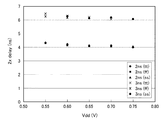
図5は、電源電圧Vddに対する基準信号の立ち上がりからセンスアンプ回路活性化信号の立ち上がりまでの時間の関係を示すシミュレーション結果である。 FIG. 5 is a simulation result showing a time relationship from the rising edge of the reference signal to the rising edge of the sense amplifier circuit activation signal with respect to the power supply voltage Vdd.
シミュレーション条件は、基準信号の立ち上がりからレプリカ遅延信号の立ち上がりまでの時間(以下、「レプリカ遅延時間」と呼ぶ)を2ns、3ns、PMOSトランジスタ及びNMOSトランジスタのプロセス条件を共にTypical(図中“tt”)、Fast(図中“ff”)、及びSlow(図中“ss”)としている。 The simulation condition is that the time from the rising edge of the reference signal to the rising edge of the replica delay signal (hereinafter referred to as “replica delay time”) is 2 ns, 3 ns, and the process conditions of the PMOS transistor and NMOS transistor are both typical (“tt” in the figure). ), Fast (“ff” in the figure), and Slow (“ss” in the figure).
図5から明らかなように、レプリカ遅延時間が2nsであった場合、トランジスタの条件及び電源電圧Vddに依らず、おおよそ2nsの2倍である4ns(図5中点線で表示)の遅延時間が得られることが分かる。また、レプリカ遅延時間が3nsであった場合でも、トランジスタの条件及び電源電圧Vddに依らず、おおよそ3nsの2倍である6nsの遅延時間が得られていることが分かる。 As is clear from FIG. 5, when the replica delay time is 2 ns, a delay time of 4 ns (indicated by a dotted line in FIG. 5), which is approximately twice 2 ns, is obtained regardless of the transistor conditions and the power supply voltage Vdd. I understand that It can also be seen that even when the replica delay time is 3 ns, a delay time of 6 ns, which is approximately twice 2 ns, is obtained regardless of the transistor conditions and the power supply voltage Vdd.
図6は、電源電圧Vddとビット線対間の電位差ΔVblとの関係を示すシミュレーション結果である。 FIG. 6 is a simulation result showing the relationship between the power supply voltage Vdd and the potential difference ΔVbl between the bit line pair.
比較例として、インバータで構成された遅延回路に対するシミュレーション結果も併せて示す。図6中、“LP”は、低電圧プロセスのトランジスタでインバータを構成した場合、“HS”はハイスピードプロセスのトランジスタでインバータを構成した場合の遅延回路に対する結果となっている。 As a comparative example, simulation results for a delay circuit composed of inverters are also shown. In FIG. 6, “LP” is the result for the delay circuit when the inverter is composed of low-voltage process transistors, and “HS” is the result for the delay circuit when the inverter is composed of high-speed process transistors.
ここで、タイミング発生回路100、あるいは比較例に係る遅延回路を設ける目的は、ビット線BL、/BL間の電位差ΔVblが最適な値となったタイミングで、センスアンプ回路を活性化させることにある。この点、トランジスタのプロセス条件、電源電圧Vddに依らずこの電位差ΔVblが一定であることが望ましい。
Here, the purpose of providing the
比較例に係る“HS”の遅延回路の場合、電源電圧Vddの変化による電位差ΔVblの変化が大きい。例えば、トランジスタのプロセス条件が“ff”であった場合、Vdd=0.4Vのとき、ΔVbl≒0.06Vであるのに対し、Vdd=0.7Vのとき、ΔVbl≒0.38Vとなっている。つまり両者のΔVblの開きは、およそ0.32Vとなる。また、トランジスタのプロセス条件の変化による電位差ΔVblの変化も大きい。例えば、電源電圧Vdd=0.4Vのとき、プロセス条件が“ss”と“ff”の場合のΔVblの開きは、およそ0.32Vにもなる。結果として、ΔVblが最小の時(Vdd=0.4V、プロセス条件“ff”)と最大の時(Vdd=0.7V、プロセス条件“ss”)とのΔVblの開きは、およそ0.6Vにもなる。 In the case of the “HS” delay circuit according to the comparative example, the change in the potential difference ΔVbl due to the change in the power supply voltage Vdd is large. For example, when the transistor process condition is “ff”, ΔVbl≈0.06V when Vdd = 0.4V, whereas ΔVbl≈0.38V when Vdd = 0.7V. Yes. That is, the opening of both ΔVbl is about 0.32V. Further, the change in the potential difference ΔVbl due to the change in the transistor process conditions is also large. For example, when the power supply voltage Vdd = 0.4V, the opening of ΔVbl when the process conditions are “ss” and “ff” is about 0.32V. As a result, when ΔVbl is minimum (Vdd = 0.4V, process condition “ff”) and maximum (Vdd = 0.7V, process condition “ss”), the opening of ΔVbl is approximately 0.6V. Also become.
一方、比較例に係る“LP”の遅延回路の場合、“HS”の遅延回路に比べ良好である。電源電圧Vddが0.4Vから0.7Vまで変化した場合のΔVblの開きが最も大きいプロセス条件が“ss”の場合であっても、およそ0.23Vとなっている。しかし、プロセス条件の変化によるΔVblの変化は、電源電圧Vddによっては、“HS”の遅延回路よりも悪い。具体的には、電源電圧Vdd=0.4Vのとき、プロセス条件が“ss”と“ff”の場合のΔVblの開きは、およそ0.37Vにもなる。結果として、ΔVblが最小の時(Vdd=0.4V、プロセス条件“ff”)と最大の時(Vdd=0.4V、プロセス条件“ss”)とのΔVblの開きは、およそ0.37Vにもなる。 On the other hand, the “LP” delay circuit according to the comparative example is better than the “HS” delay circuit. Even when the process condition with the largest opening of ΔVbl when the power supply voltage Vdd changes from 0.4 V to 0.7 V is “ss”, it is about 0.23 V. However, the change in ΔVbl due to the change in the process condition is worse than that of the “HS” delay circuit depending on the power supply voltage Vdd. Specifically, when the power supply voltage Vdd = 0.4V, the opening of ΔVbl when the process conditions are “ss” and “ff” is about 0.37V. As a result, the opening of ΔVbl when ΔVbl is minimum (Vdd = 0.4V, process condition “ff”) and maximum (Vdd = 0.4V, process condition “ss”) is about 0.37V. Also become.
この点、本実施形態によれば、比較例に係る遅延回路と比較し、電源電圧Vdd及びプロセス条件の変化によるビット線BL、/BL間の電位差ΔVblの差が小さいことが分かる。例えば、電源電圧Vddが0.4Vから0.7Vに変化したときのΔVblの変化の開きが一番大きいプロセス条件が“ss”の場合であっても、およそ0.18Vしかない。また、プロセス条件の変化したときのΔVblの変化の開きが一番大きい電源電圧Vdd=0.7Vの場合であっても、およそ0.22Vに抑えられている。結果として、ΔVblが最小の時(Vdd=0.4V、プロセス条件“ff”)と最大の時(Vdd=0.7V、プロセス条件“ss”)とのΔVblの開きは、およそ0.32Vである。 In this regard, according to the present embodiment, it can be seen that the difference in the potential difference ΔVbl between the bit lines BL and / BL due to the change in the power supply voltage Vdd and the process conditions is small as compared with the delay circuit according to the comparative example. For example, even when the process condition with the largest change in ΔVbl when the power supply voltage Vdd is changed from 0.4 V to 0.7 V is “ss”, it is only about 0.18 V. Further, even when the power supply voltage Vdd = 0.7V has the largest variation in ΔVbl when the process condition changes, it is suppressed to about 0.22V. As a result, the opening of ΔVbl when ΔVbl is minimum (Vdd = 0.4V, process condition “ff”) and maximum (Vdd = 0.7V, process condition “ss”) is approximately 0.32V. is there.
図7は、タイミング発生回路100をハイスピードプロセスのトランジスタで構成した場合、及び低電圧プロセスのトランジスタで構成した場合における電源電圧Vddとステップ数増減による遅延時間の増減率の関係を示すシミュレーション結果である。
FIG. 7 is a simulation result showing the relationship between the power supply voltage Vdd and the increase / decrease rate of the delay time due to the increase / decrease in the number of steps in the case where the
往路回路100aによるレプリカ遅延時間の量子化のステップ時間を細かくしたい場合、閾値が小さく、生じる遅延が小さいハイスピードプロセスのトランジスタで構成すれば良い。しかし、図6の結果からもわかるようにハイスピードプロセスのトランジスタは、電源電圧Vddの変化に弱いことが欠点である。その点、図7から明らかなように、本実施形態の場合、往路回路100aによりレプリカ遅延時間を量子化し、それと同等の時間を復路回路100bにより付加するものである。したがって、電源電圧Vddの変化に伴い量子化のステップ時間は変動するものの、ステップ数増減による遅延時間の変化率はほぼ一定である。これは、ハイスピードプロセス、低電圧プロセス問わず、電源電圧Vddの変化に対する安定性が高いことを示すものである。
When the quantization delay time of the replica delay time by the
以上の通り、本実施形態によれば、メモリセルアレイの特性の変化に伴うレプリカ回路への影響をそのまま反映してセルアレイ回路活性化信号を生成しているため、電源電圧の変化等、環境変化に応じた最適なセンスアンプ回路の活性化を実現することができる。 As described above, according to the present embodiment, the cell array circuit activation signal is generated by directly reflecting the influence on the replica circuit due to the change in the characteristics of the memory cell array. Accordingly, the activation of the optimum sense amplifier circuit can be realized.
また、本実施形態のタイミング発生回路100は、あらゆる条件のトランジスタであっても安定した特性を有する。そのため、本実施形態によれば、製造プロセスのばらつきによる影響が少なく、また、設計変更等にも柔軟に対応するこができる。
In addition, the
[第2の実施形態]
図8は、本発明の第2の実施形態に係る半導体記憶装置のタイミング発生回路200である。
[Second Embodiment]
FIG. 8 shows a
このタイミング発生回路200は、レプリカ遅延時間を3倍にする回路である。
The
往路回路200aは、タイミング発生回路100の場合と同様、1ステージ毎に、1個のNANDゲート(G203など)と1個のインバータ(G204など)を備えている。
As in the case of the
一方、復路回路200bは、1ステップ毎に、例えば、ノードNC0及びNC1間の場合、NANDゲートG218、インバータG219、NANDゲートG221、インバータG222で構成されている。言い換えれば、ノードNC0及びインバータG219の出力端であるノードNC0´間、並びにノードNC0´及びノードNC1間は、それぞれ往路回路200aの1ステージを構成するものである。つまり、復路回路200bのステップ時間は、往路回路200aのステップ時間の2倍となる。
On the other hand, the
結果として、レプリカ遅延時間のおよそ3倍を持つセンスアンプ回路活性化信号SAENBLを生成することができる。 As a result, the sense amplifier circuit activation signal SAENBL having about three times the replica delay time can be generated.
本実施形態のように、1ステージ毎の往路回路と復路回路のゲート数の比を変更することで、任意のタイミングでセンスアンプ回路を活性化するセンスアンプ回路活性化信号を生成することができる。 As in the present embodiment, the sense amplifier circuit activation signal for activating the sense amplifier circuit can be generated at an arbitrary timing by changing the ratio of the number of gates of the forward circuit and the backward circuit for each stage. .
[第3の実施形態]
図9は、本発明の第3の実施形態に係る半導体記憶装置のタイミング発生回路300の回路図である。
[Third Embodiment]
FIG. 9 is a circuit diagram of the
このタイミング発生回路300は、ステップ時間を小さくしたい場合の実施形態である。
This
ステップ時間を小さくする場合、往路回路300a、復路回路300bの1ステージ毎のゲート数を減らしてやれば良い。
In order to reduce the step time, the number of gates for each stage of the
タイミング発生回路300の場合、先に説明したタイミング発生回路100、200に対し、ステージ毎に設けられたインバータを削減している。この場合、ノードNAi(i=偶数)とノードNAi+1では論理が逆転するため、ノードNA1、NA3、・・・が入力端に接続されたNANDゲートG303、G307、・・・の他方の入力端には、レプリカ遅延信号と逆論理の信号が入力されている。
In the case of the
以上のように、本実施形態によれば、第1及び第2の実施形態に比べ、ステップ時間を小さくすることができるため、レプリカ遅延時間の量子化誤差が小さくなり、より最適なセンスアンプ回路の活性化タイミングを発生させることができる。 As described above, according to the present embodiment, since the step time can be reduced compared to the first and second embodiments, the quantization error of the replica delay time is reduced, and a more optimal sense amplifier circuit. Activation timing can be generated.
[その他]
以上、発明の実施の形態としてSRAMを取り上げ説明したが、本発明はSRAMに限定されるものではなく、DRAM、フラッシュメモリ等あらゆる半導体記憶装置に適用することができる。
[Others]
As described above, the SRAM has been described as an embodiment of the invention. However, the present invention is not limited to the SRAM, and can be applied to any semiconductor memory device such as a DRAM and a flash memory.
なお、以上の各実施形態での他の特徴点を列挙すれば、以下の通りである。 In addition, it will be as follows if the other feature point in each above embodiment is enumerated.
(1) タイミング発生回路は、複数のステージからなる復路回路を備え、往路回路の量子化の結果に基づいて、ステージ毎に生じる遅延時間単位でセンスアンプ回路の活性化タイミングを調整することを特徴とする。 (1) The timing generation circuit includes a return circuit composed of a plurality of stages, and adjusts the activation timing of the sense amplifier circuit in units of delay time generated for each stage based on the quantization result of the forward circuit. And
(2) 往路回路のステージと、復路回路のステージを構成するゲート数が同じであることを特徴とする。 (2) The number of gates constituting the stage of the forward circuit and the stage of the backward circuit are the same.
(3) 往路回路のステージと、復路回路のステージを構成するゲート数が異なることを特徴とする。 (3) The number of gates constituting the stage of the forward circuit and the stage of the backward circuit are different.
100、200、300・・・タイミング発生回路、100a、200a、300a・・・往路回路、100b、200b、300b・・・復路回路。 100, 200, 300... Timing generation circuit, 100a, 200a, 300a... Outward circuit, 100b, 200b, 300b.
Claims (4)
前記ビット線の信号レベルを検知・増幅する複数のセンスアンプ回路と、
レプリカワード線、前記レプリカワード線に交差するレプリカビット線、前記レプリカワード線及びレプリカビット線の各交差部に設けられたレプリカメモリセルからなり、前記メモリセルの読み出し動作を模擬するレプリカ回路と、
基準タイミングから前記レプリカビット線が変化するまでの時間であるレプリカ遅延時間を量子化し、その結果に基づいて、前記センスアンプ回路の活性化タイミングを生成するタイミング発生回路と
を有し、
前記タイミング発生回路は、
所定数のゲートからなる単位回路(ステージ)を複数接続してなる往路回路を備え、
前記基本タイミングが前記複数のステージを順次伝搬されるタイミングと、前記レプリカビット線が変化するタイミングとを比較し、前記ステージ毎に生じる遅延時間単位で前記レプリカ遅延時間を量子化する
ことを特徴とする半導体記憶装置。 A memory cell array comprising a plurality of word lines, a plurality of bit lines intersecting the word lines, a plurality of memory cells provided at each intersection of the word lines and the bit lines;
A plurality of sense amplifier circuits for detecting and amplifying the signal level of the bit line;
A replica word line, a replica bit line that intersects the replica word line, a replica memory cell provided at each intersection of the replica word line and the replica bit line, and a replica circuit that simulates a read operation of the memory cell;
A timing generation circuit that quantizes a replica delay time, which is a time from a reference timing until the replica bit line changes, and generates an activation timing of the sense amplifier circuit based on the result;
Have
The timing generation circuit includes:
A forward circuit comprising a plurality of unit circuits (stages) each having a predetermined number of gates,
Comparing the timing at which the basic timing is sequentially propagated through the plurality of stages with the timing at which the replica bit line is changed, and quantizing the replica delay time in units of delay time generated for each stage, semiconductors storage you.
前記ビット線の信号レベルを検知・増幅する複数のセンスアンプ回路と、
レプリカワード線、前記レプリカワード線に交差するレプリカビット線、前記レプリカワード線及びレプリカビット線の各交差部に設けられたレプリカメモリセルからなり、前記メモリセルの読み出し動作を模擬するレプリカ回路と、
基準タイミングから前記レプリカビット線が変化するまでの時間であるレプリカ遅延時間を量子化し、その結果に基づいて、前記センスアンプ回路の活性化タイミングを生成するタイミング発生回路と
を有し、
前記タイミング発生回路は、
前記基準タイミングを入力する縦続接続された第1及び第2のゲート、並びに、前記第2のゲートの出力が第1の入力端に入力され、前記レプリカビット線が変化するタイミングが第2の入力端に入力される第3のゲートを備えた第1の単位回路(ステージ)を複数縦続接続してなる往路回路と、
縦続接続された第4及び第5のゲートを備えた第2の単位回路(ステージ)を有し、前記第2の単位回路は、前記第1の単位回路と対応させて複数縦続接続され、前記第4のゲートの第1の入力端に前記第3のゲートの出力が入力され、前記第4のゲートの第2の入力端に前段の前記第2の単位回路の出力が入力され、最終段の前記第2の単位回路の出力の変化から、前記センスアンプ回路の活性化タイミングを生成する復路回路と
を有する
ことを特徴とする半導体記憶装置。 A memory cell array comprising a plurality of word lines, a plurality of bit lines intersecting the word lines, a plurality of memory cells provided at each intersection of the word lines and the bit lines;
A plurality of sense amplifier circuits for detecting and amplifying the signal level of the bit line;
A replica word line, a replica bit line that intersects the replica word line, a replica memory cell provided at each intersection of the replica word line and the replica bit line, and a replica circuit that simulates a read operation of the memory cell;
A timing generation circuit that quantizes a replica delay time, which is a time from a reference timing until the replica bit line changes, and generates an activation timing of the sense amplifier circuit based on the result;
Have
The timing generation circuit includes:
The first and second gates connected in cascade to input the reference timing, and the output of the second gate are input to the first input terminal, and the timing at which the replica bit line changes is the second input. A forward circuit formed by cascading a plurality of first unit circuits (stages) each having a third gate that is input to the end;
A second unit circuit (stage) having fourth and fifth gates connected in cascade; a plurality of the second unit circuits connected in cascade with the first unit circuit; The output of the third gate is input to the first input terminal of the fourth gate, the output of the second unit circuit of the previous stage is input to the second input terminal of the fourth gate, and the final stage from the change in the output of the second unit circuit, semi-conductor memory device you; and a recovery path circuitry for generating an activation timing of the sense amplifier circuit.
前記ビット線の信号レベルを検知・増幅する複数のセンスアンプ回路と、
レプリカワード線、前記レプリカワード線に交差するレプリカビット線、前記レプリカワード線及びレプリカビット線の各交差部に設けられたレプリカメモリセルからなり、前記メモリセルの読み出し動作を模擬するレプリカ回路と、
基準タイミングから前記レプリカビット線が変化するまでの時間であるレプリカ遅延時間を量子化し、その結果に基づいて、前記センスアンプ回路の活性化タイミングを生成するタイミング発生回路と
を有し、
前記タイミング発生回路は、
前記基準タイミングを入力する縦続接続された第1及び第2のゲート、並びに、前記第2のゲートの出力が第1の入力端に入力され、前記レプリカビット線が変化するタイミングが第2の入力端に入力される第3のゲートを備えた第1の単位回路(ステージ)を複数縦続接続してなる往路回路と、
縦続接続された第4乃至第7のゲートを備えた第2の単位回路(ステージ)を有し、前記第2の単位回路は、前記第1の単位回路と対応させて複数縦続接続され、前記第4のゲートの第1の入力端に前記第3のゲートの出力が入力され、前記第4のゲートの第2の入力端に前段の前記第2の単位回路の出力が入力され、最終段の前記第2の単位回路の出力の変化から、前記センスアンプ回路の活性化タイミングを生成する復路回路と
を有する
ことを特徴とする半導体記憶装置。 A memory cell array comprising a plurality of word lines, a plurality of bit lines intersecting the word lines, a plurality of memory cells provided at each intersection of the word lines and the bit lines;
A plurality of sense amplifier circuits for detecting and amplifying the signal level of the bit line;
A replica word line, a replica bit line that intersects the replica word line, a replica memory cell provided at each intersection of the replica word line and the replica bit line, and a replica circuit that simulates a read operation of the memory cell;
A timing generation circuit that quantizes a replica delay time, which is a time from a reference timing until the replica bit line changes, and generates an activation timing of the sense amplifier circuit based on the result;
Have
The timing generation circuit includes:
The first and second gates connected in cascade to input the reference timing, and the output of the second gate are input to the first input terminal, and the timing at which the replica bit line changes is the second input. A forward circuit formed by cascading a plurality of first unit circuits (stages) each having a third gate that is input to the end;
A second unit circuit (stage) including fourth to seventh gates connected in cascade; a plurality of the second unit circuits connected in cascade with the first unit circuit; The output of the third gate is input to the first input terminal of the fourth gate, the output of the second unit circuit of the previous stage is input to the second input terminal of the fourth gate, and the final stage from the change in the output of the second unit circuit, semi-conductor memory device you; and a recovery path circuitry for generating an activation timing of the sense amplifier circuit.
前記ビット線の信号レベルを検知・増幅する複数のセンスアンプ回路と、
レプリカワード線、前記レプリカワード線に交差するレプリカビット線、前記レプリカワード線及びレプリカビット線の各交差部に設けられたレプリカメモリセルからなり、前記メモリセルの読み出し動作を模擬するレプリカ回路と、
基準タイミングから前記レプリカビット線が変化するまでの時間であるレプリカ遅延時間を量子化し、その結果に基づいて、前記センスアンプ回路の活性化タイミングを生成するタイミング発生回路と
を有し、
前記タイミング発生回路は、
前記基準タイミングが入力される第1のゲート、この第1のゲートの出力が第1の入力端に入力され、前記レプリカビット線が変化するタイミングが第2の入力端に入力される第2のゲートを備えた第1の単位回路(ステージ)、並びに、前記第1の単位回路の出力が入力される第3のゲート、この第3のゲートの出力が第1の入力端に入力され、前記レプリカビット線が変化するタイミングを逆論理にした信号が第2の入力端に入力される第4のゲートを備えた第2の単位回路(ステージ)を交互に複数縦続接続してなる往路回路と、
前記第1のゲートに対応する第5のゲートを備えた第3の単位回路(ステージ)、並びに、前記第3のゲートに対応する第6のゲートを備えた第4の単位回路(ステージ)が前記第1及び第2の単位回路に対応させて交互に複数縦続接続され、前記第5のゲートの第1の入力端に前記第2のゲートの出力が入力され、前記第5の第2の入力端に前段の前記第4の単位回路の出力が入力され、前記第6のゲートの第1の入力端に前記第4のゲートの出力が入力され、前記第6のゲートの第2の入力端に前段の前記第3の単位回路の出力が入力され、最終段の第4の単位回路の出力の変化から、前記センスアンプ回路の活性化タイミングを生成する復路回路と
を有する
ことを特徴とする半導体記憶装置。
A memory cell array comprising a plurality of word lines, a plurality of bit lines intersecting the word lines, a plurality of memory cells provided at each intersection of the word lines and the bit lines;
A plurality of sense amplifier circuits for detecting and amplifying the signal level of the bit line;
A replica word line, a replica bit line that intersects the replica word line, a replica memory cell provided at each intersection of the replica word line and the replica bit line, and a replica circuit that simulates a read operation of the memory cell;
A timing generation circuit that quantizes a replica delay time, which is a time from a reference timing until the replica bit line changes, and generates an activation timing of the sense amplifier circuit based on the result;
Have
The timing generation circuit includes:
A first gate to which the reference timing is input, an output of the first gate is input to a first input terminal, and a timing at which the replica bit line changes is input to a second input terminal. A first unit circuit (stage) including a gate; a third gate to which an output of the first unit circuit is input; an output of the third gate is input to a first input terminal; A forward circuit formed by alternately cascading a plurality of second unit circuits (stages) each having a fourth gate in which a signal whose timing of changing a replica bit line is inverted is input to a second input terminal; ,
A third unit circuit (stage) having a fifth gate corresponding to the first gate, and a fourth unit circuit (stage) having a sixth gate corresponding to the third gate; A plurality of cascade connections are alternately made in correspondence with the first and second unit circuits, the output of the second gate is input to the first input terminal of the fifth gate, and the fifth second The output of the fourth unit circuit in the previous stage is input to the input terminal, the output of the fourth gate is input to the first input terminal of the sixth gate, and the second input of the sixth gate end output of the third unit circuit of the preceding stage is input to, characterized in that the change in the output of the fourth unit circuit of the final stage, and a recovery path circuitry for generating an activation timing of the sense amplifier circuit It shall be the semi-conductor storage device.
Priority Applications (2)
| Application Number | Priority Date | Filing Date | Title |
|---|---|---|---|
| JP2008333972A JP5259382B2 (en) | 2008-12-26 | 2008-12-26 | Semiconductor memory device |
| US12/643,925 US8111571B2 (en) | 2008-12-26 | 2009-12-21 | Semiconductor memory device |
Applications Claiming Priority (1)
| Application Number | Priority Date | Filing Date | Title |
|---|---|---|---|
| JP2008333972A JP5259382B2 (en) | 2008-12-26 | 2008-12-26 | Semiconductor memory device |
Publications (2)
| Publication Number | Publication Date |
|---|---|
| JP2010157279A JP2010157279A (en) | 2010-07-15 |
| JP5259382B2 true JP5259382B2 (en) | 2013-08-07 |
Family
ID=42284805
Family Applications (1)
| Application Number | Title | Priority Date | Filing Date |
|---|---|---|---|
| JP2008333972A Expired - Fee Related JP5259382B2 (en) | 2008-12-26 | 2008-12-26 | Semiconductor memory device |
Country Status (2)
| Country | Link |
|---|---|
| US (1) | US8111571B2 (en) |
| JP (1) | JP5259382B2 (en) |
Families Citing this family (4)
| Publication number | Priority date | Publication date | Assignee | Title |
|---|---|---|---|---|
| JP5404584B2 (en) | 2010-11-19 | 2014-02-05 | 株式会社東芝 | Semiconductor memory device |
| JP5917219B2 (en) | 2012-03-21 | 2016-05-11 | 株式会社東芝 | Semiconductor memory device |
| US9318190B1 (en) | 2014-09-30 | 2016-04-19 | Taiwan Semiconductor Manufacturing Co., Ltd. | Memory device |
| CN112542185B (en) * | 2019-09-20 | 2024-05-14 | 长鑫存储技术有限公司 | Sense amplifier, control method thereof, memory read-write circuit and memory |
Family Cites Families (8)
| Publication number | Priority date | Publication date | Assignee | Title |
|---|---|---|---|---|
| JP3542225B2 (en) | 1996-03-19 | 2004-07-14 | 株式会社日立製作所 | Semiconductor device |
| JPH09282889A (en) * | 1996-04-09 | 1997-10-31 | Toshiba Corp | Semiconductor device |
| JPH11203877A (en) * | 1998-01-19 | 1999-07-30 | Hitachi Ltd | Semiconductor integrated circuit and design method thereof |
| JP2002216481A (en) * | 2001-01-19 | 2002-08-02 | Hitachi Ltd | Semiconductor integrated circuit device |
| JP3699920B2 (en) * | 2001-10-25 | 2005-09-28 | 株式会社東芝 | Delay circuit and synchronous delay device |
| JP2004022070A (en) * | 2002-06-17 | 2004-01-22 | Renesas Technology Corp | Semiconductor storage device |
| US7042776B2 (en) * | 2004-02-18 | 2006-05-09 | International Business Machines Corporation | Method and circuit for dynamic read margin control of a memory array |
| US7061793B2 (en) * | 2004-03-19 | 2006-06-13 | International Business Machines Corporation | Apparatus and method for small signal sensing in an SRAM cell utilizing PFET access devices |
-
2008
- 2008-12-26 JP JP2008333972A patent/JP5259382B2/en not_active Expired - Fee Related
-
2009
- 2009-12-21 US US12/643,925 patent/US8111571B2/en active Active
Also Published As
| Publication number | Publication date |
|---|---|
| US8111571B2 (en) | 2012-02-07 |
| JP2010157279A (en) | 2010-07-15 |
| US20100165771A1 (en) | 2010-07-01 |
Similar Documents
| Publication | Publication Date | Title |
|---|---|---|
| KR102408572B1 (en) | Semiconductor memory device | |
| CN102150213B (en) | Circuit and method for optimizing memory sense amplifier timing | |
| KR102424285B1 (en) | Multi level sensing circuit and semiconductor device including the same | |
| JP5478772B2 (en) | Low power 5TSRAM with improved stability and reduced bit cell size | |
| CN110660419B (en) | Memory circuit and method of operating the same | |
| US8208336B2 (en) | Fuse circuit and semiconductor device having the same | |
| US8116119B1 (en) | Desensitizing static random access memory (SRAM) to process variations | |
| CN101667452A (en) | Semiconductor device | |
| CN110890119B (en) | Voltage generation circuit, memory device and method of generating bit line precharge voltage | |
| JP4960419B2 (en) | Semiconductor memory device and semiconductor device | |
| KR102532606B1 (en) | Electronic device for configuring neural network | |
| US9099168B2 (en) | Method for extending word-line pulses | |
| JP4090967B2 (en) | Semiconductor memory device | |
| JP5259382B2 (en) | Semiconductor memory device | |
| US9431094B1 (en) | Input buffer | |
| US20190172507A1 (en) | Apparatuses and methods for providing bias signals in a semiconductor device | |
| US9001613B2 (en) | Tracking mechanisms | |
| US6707741B1 (en) | Current steering reduced bitline voltage swing, sense amplifier | |
| JP5404584B2 (en) | Semiconductor memory device | |
| US8619478B2 (en) | System and method for generating a clock | |
| US10373655B2 (en) | Apparatuses and methods for providing bias signals according to operation modes as supply voltages vary in a semiconductor device | |
| KR100884761B1 (en) | Sense amplifier enable signal generation circuit, memory device having same and method for generating sense amplifier enable signal | |
| KR102815077B1 (en) | Pulse Signal Generator to reduce Power Consumption of SRAM and SRAM having The Same | |
| KR100771545B1 (en) | Sense Amplifier Control Signal Generation Circuit | |
| TWI869917B (en) | Memory device, sense amplifier system, and method for operating memory array |
Legal Events
| Date | Code | Title | Description |
|---|---|---|---|
| A621 | Written request for application examination |
Free format text: JAPANESE INTERMEDIATE CODE: A621 Effective date: 20110314 |
|
| A977 | Report on retrieval |
Free format text: JAPANESE INTERMEDIATE CODE: A971007 Effective date: 20121010 |
|
| A131 | Notification of reasons for refusal |
Free format text: JAPANESE INTERMEDIATE CODE: A131 Effective date: 20121023 |
|
| A521 | Request for written amendment filed |
Free format text: JAPANESE INTERMEDIATE CODE: A523 Effective date: 20121212 |
|
| RD01 | Notification of change of attorney |
Free format text: JAPANESE INTERMEDIATE CODE: A7421 Effective date: 20130221 |
|
| TRDD | Decision of grant or rejection written | ||
| A01 | Written decision to grant a patent or to grant a registration (utility model) |
Free format text: JAPANESE INTERMEDIATE CODE: A01 Effective date: 20130402 |
|
| A61 | First payment of annual fees (during grant procedure) |
Free format text: JAPANESE INTERMEDIATE CODE: A61 Effective date: 20130424 |
|
| FPAY | Renewal fee payment (event date is renewal date of database) |
Free format text: PAYMENT UNTIL: 20160502 Year of fee payment: 3 |
|
| LAPS | Cancellation because of no payment of annual fees |