JP5259333B2 - Waveform equalization amount adjustment method, waveform equalization amount adjustment circuit, semiconductor device, and information network device - Google Patents
Waveform equalization amount adjustment method, waveform equalization amount adjustment circuit, semiconductor device, and information network device Download PDFInfo
- Publication number
- JP5259333B2 JP5259333B2 JP2008267825A JP2008267825A JP5259333B2 JP 5259333 B2 JP5259333 B2 JP 5259333B2 JP 2008267825 A JP2008267825 A JP 2008267825A JP 2008267825 A JP2008267825 A JP 2008267825A JP 5259333 B2 JP5259333 B2 JP 5259333B2
- Authority
- JP
- Japan
- Prior art keywords
- data
- timing
- signal
- waveform equalization
- equalization amount
- Prior art date
- Legal status (The legal status is an assumption and is not a legal conclusion. Google has not performed a legal analysis and makes no representation as to the accuracy of the status listed.)
- Expired - Fee Related
Links
Images


Landscapes
- Dc Digital Transmission (AREA)
- Cable Transmission Systems, Equalization Of Radio And Reduction Of Echo (AREA)
Description
本発明は、波形等化量調整方法、波形等化量調整回路、半導体装置および情報ネットワーク装置係り、特に、ルータ、サーバ、PCなどの情報ネットワーク装置および情報端末機器に適用する波形等化量調整方法および波形等化量調整回路ならびに半導体装置および情報ネットワーク装置に関する。 The present invention relates to a waveform equalization amount adjustment method, a waveform equalization amount adjustment circuit, a semiconductor device, and an information network device, and more particularly to a waveform equalization amount adjustment applied to information network devices and information terminal devices such as routers, servers, and PCs. The present invention relates to a method, a waveform equalization amount adjusting circuit, a semiconductor device, and an information network device.
近年、情報ネットワークのトラフィック量の増加により、サーバおよびルータに代表される情報ネットワーク装置において、LSI間でデータ通信を行うためのインターフェースの伝送速度が増加(10Gb/s〜)している。このような伝送速度の増加に伴い、LSI間を電気的に接続する基板、コネクタ、LSIパッケージ、ケーブルなどにおける伝送損失が増加し、伝送波形の歪みが顕著になる。このことから、波形歪みを補償する波形等化回路がLSIに搭載されている。この波形等化回路において、基板配線長、LSIの製造ばらつきなどに応じて適正な波形等化量が異なることから、波形等化量を自動で最適化する技術が必要とされている。 In recent years, with an increase in the amount of traffic in an information network, in an information network device represented by a server and a router, the transmission speed of an interface for performing data communication between LSIs has increased (from 10 Gb / s). Along with such an increase in transmission speed, transmission loss in substrates, connectors, LSI packages, cables, etc. that electrically connect LSIs increases, and transmission waveform distortion becomes noticeable. For this reason, a waveform equalization circuit that compensates for waveform distortion is mounted on the LSI. In this waveform equalization circuit, the appropriate waveform equalization amount varies depending on the substrate wiring length, the manufacturing variation of the LSI, etc., and therefore a technique for automatically optimizing the waveform equalization amount is required.
図1を参照して、波形等化量の調整機能を搭載するLSIおよびLSI間接続の一般的な構成を説明する。図1において、2台のLSI201は、伝送路206と伝送路207とで相互接続されている。LSI201は、高速信号を送信するためのドライバ202と、高速信号を受信するためのレシーバ203と、比較的低速な信号を送受信するためのI/O回路205と、I/O回路205およびレシーバ203で受信した信号を演算処理する論理回路204とで構成され、LSI間は伝送路206、207で接続されている。また、波形等化回路は、レシーバ203に搭載されており、論理回路204から出力される調整信号により、波形等化量が調整される。
With reference to FIG. 1, a general configuration of an LSI on which a function for adjusting the waveform equalization amount and an inter-LSI connection are mounted will be described. In FIG. 1, two LSIs 201 are interconnected by a
波形等化量の調整フローは、以下の通りである。LSI201−1のドライバ202−1から出力されたデータは、伝送路206を介して、対向するLSI201−2のレシーバ203−2にて受信される。同様に、LSI201−2のドライバ202−2から出力されたデータは、伝送路206を介して、対向するLSI201−1のレシーバ203−1にて受信される。LSI201は、受信したデータを、論理回路204で演算処理して波形等化量の過不足状態を判別し、結果に応じた波形等化量の調整信号を、自LSI201のレシーバ203に送信する。波長等化量の調整信号は、自レシーバを介して、対向LSIのドライバ、また、I/O回路を介して、対向するLSIに送信される。上記フローにより、波形等化量が自動的に調整される。
The adjustment flow of the waveform equalization amount is as follows. Data output from the driver 202-1 of the LSI 201-1 is received by the receiver 203-2 of the opposing LSI 201-2 via the
図2を参照して、波形等化量の過不足状態の判別および波形等化量の調整信号を出力する背景技術の波形等化量調整回路の機能ブロックを説明する。図2において、波形等化量調整回路800は、データ取得部801、トレーニングデータ生成部802、パタン同期部803、データパタン評価部804、Up/Down信号カウント部805、取得データカウント部806、Up/Down信号差分評価部807から構成される。
With reference to FIG. 2, a functional block of a waveform equalization amount adjustment circuit of the background art that determines whether the waveform equalization amount is excessive or insufficient and outputs a waveform equalization amount adjustment signal will be described. In FIG. 2, the waveform equalization
データ取得部801は、受信データから、波形等化量を調整するために必要となるデータを取得する。トレーニングデータ生成部802は、送信LSIで生成されたデータと同一のトレーニングデータを生成する。パタン同期部803は、取得データとトレーニングデータとの同期を取る。データパタン評価部804は、取得データとトレーニングデータとのデータパタンを比較して波形等化量が過剰の(強い)場合にはDown信号を、不足(弱い)の場合にはUp信号を出力する。Up/Down信号カウント部805は、Up/Down信号の数をカウントする。取得データカウント部806は、データ取得部801で取得したデータの数をカウントして所定のカウント数を満たしているかを評価する。Up/Down信号差分評価部807は、カウントしたUp/Down信号の数の差分と所定の差分しきい値を比較して波形等化量調整信号を出力する。
The
上述したデータパタン評価部804は、波形等化量の過不足を評価する方法として一般的にLMS(Least Mean Square:最小二乗法)アルゴリズムが用いられる。
特許文献1には、波形等化器の等化係数(タップ係数)を、パタン発生器を用いたトレーニングで求める発明が記載されている。
The data
上述した波形等化量調整回路ではトレーニングデータを必要とする。このため、たとえば回路特性の経時変化などにより波形等化量の最適値が変化した場合には、一旦、装置をトレーニング動作に切り替えて波形等化量を再調整する必要がある。すなわち、装置の通常動作を停止させる必要がある。また、トレーニングデータ生成部およびパタン同期部などの、装置の通常動作時には不要な機能を付加する必要がある。このため、LSIの回路規模が大きくなるという問題がある。
本発明の目的は、上記課題を解決する波形等化量調整方法および波形等化量調整回路ならびに半導体装置および情報ネットワーク装置を提供することにある。
The waveform equalization amount adjusting circuit described above requires training data. For this reason, when the optimum value of the waveform equalization amount changes due to, for example, a change in circuit characteristics over time, it is necessary to once readjust the waveform equalization amount by switching the apparatus to a training operation. That is, it is necessary to stop the normal operation of the apparatus. Further, it is necessary to add unnecessary functions such as a training data generation unit and a pattern synchronization unit during normal operation of the apparatus. For this reason, there exists a problem that the circuit scale of LSI becomes large.
An object of the present invention is to provide a waveform equalization amount adjustment method, a waveform equalization amount adjustment circuit, a semiconductor device, and an information network device that solve the above-described problems.
上述した課題は、レシーバにて受信したデータにおいて、クロック再生部で再生されたクロックで取得したデータと、再生クロックとは異なる位相のクロックで取得したデータとのデータパタンを評価することで、波形等化量を調整する波形等化量調整方法および波形等化量調整回路により、達成できる。 The problem described above is that, in the data received by the receiver, the waveform obtained by evaluating the data pattern of the data acquired by the clock recovered by the clock recovery unit and the data acquired by the clock having a phase different from that of the recovered clock. This can be achieved by the waveform equalization amount adjustment method and the waveform equalization amount adjustment circuit for adjusting the equalization amount.
また、通信用のインターフェースを備え、受信データに係る波形等化量を調整するためのデータを取得するデータ取得部と、取得したデータのデータパタンを評価してUp信号とDown信号とを出力するデータパタン評価部と、Up信号とDown信号との数をカウントするUp/Down信号カウント部と、データ取得部で取得したデータの数をカウントして所定のカウント数を満たしているかを評価する取得データ数判定部と、カウントしたUp信号の数とDown信号の数の差分と所定の差分しきい値を比較して波形等化量調整信号を出力するUp/Down信号差分評価部とで構成される波形等化量調整回路を備える半導体装置により、達成できる。 In addition, the communication interface includes a data acquisition unit that acquires data for adjusting the waveform equalization amount related to the received data, and outputs an Up signal and a Down signal by evaluating the data pattern of the acquired data. Data pattern evaluation unit, Up / Down signal count unit that counts the number of Up signals and Down signals, and acquisition that counts the number of data acquired by the data acquisition unit and evaluates whether a predetermined count number is satisfied A data number determination unit and an Up / Down signal difference evaluation unit that outputs a waveform equalization amount adjustment signal by comparing a difference between the counted number of Up signals and the number of Down signals and a predetermined difference threshold value. This can be achieved by a semiconductor device including a waveform equalization amount adjusting circuit.
さらに、通信用のインターフェースを備えた半導体装置を実装する第1および第2の実装基板と、第1の実装基板と第2の実装基板とを接続されたバックプレーン基板を含み、半導体装置は、受信データに係る波形等化量を調整するためのデータを取得するデータ取得部と、取得したデータのデータパタンを評価してUp信号とDown信号とを出力するデータパタン評価部と、Up信号とDown信号との数をカウントするUp/Down信号カウント部と、データ取得部で取得したデータの数をカウントして所定のカウント数を満たしているかを評価する取得データ数判定部と、カウントしたUp信号の数とDown信号の数のと差分と所定の差分しきい値を比較して波形等化量調整信号を出力するUp/Down信号差分評価部とで構成される波形等化量調整回路を備える情報ネットワーク装置により、達成できる。 Furthermore, the semiconductor device includes first and second mounting substrates on which a semiconductor device having a communication interface is mounted, and a backplane substrate to which the first mounting substrate and the second mounting substrate are connected. A data acquisition unit that acquires data for adjusting a waveform equalization amount related to received data, a data pattern evaluation unit that evaluates a data pattern of the acquired data and outputs an Up signal and a Down signal, and an Up signal An Up / Down signal count unit that counts the number of Down signals, an acquired data number determination unit that counts the number of data acquired by the data acquisition unit and evaluates whether a predetermined count number is satisfied, and the counted Up An Up / Down signal difference evaluation unit that compares the difference between the number of signals, the number of Down signals, and a predetermined difference threshold value and outputs a waveform equalization amount adjustment signal. The information network system comprising a waveform equalizer adjustment circuit to be, can be achieved.
受信したデータのみで波形等化量を最適化できるので、小さな回路規模で実現可能である。また、回路特性の経時変化などにより波形等化量の最適値が変動した場合でも、装置を通常動作させた状態で波形等化量を最適化できる。 Since the waveform equalization amount can be optimized only by the received data, it can be realized with a small circuit scale. Even when the optimum value of the waveform equalization amount fluctuates due to a change in circuit characteristics over time, the waveform equalization amount can be optimized while the apparatus is normally operated.
以下、本発明の実施の形態について、実施例を用い、図面を参照しながら詳細に説明する。なお、実質同一部位には同じ参照番号を振り、説明は繰り返さない。 Hereinafter, embodiments of the present invention will be described in detail with reference to the drawings using examples. The same reference numerals are assigned to substantially the same parts, and the description will not be repeated.
図3を参照して、実施例1の波形等化量調整回路の機能ブロックを説明する。図3において、波形等化量調整回路100は、データ取得部101、データパタン評価部102、Up/Down信号カウント部103、取得データカウント部104、Up/Down信号差分評価部105から構成される。
With reference to FIG. 3, functional blocks of the waveform equalization amount adjusting circuit according to the first embodiment will be described. In FIG. 3, the waveform equalization
データ取得部101は、波形等化量を調整するために必要となるデータを取得する。データパタン評価部102は、取得データを評価して波形等化量が過剰な(強い)場合にはDown信号を、不足(弱い)の場合にはUp信号を出力する。Up/Down信号カウント部103は、Up/Down信号の数をカウントする。取得データカウント部104は、データ取得部101で取得したデータの数をカウントして、所定のカウント数を満たしているかを評価する。Up/Down信号差分評価部105は、カウントしたUp/Down信号の数の差分と所定の差分しきい値を比較して、波形等化量調整信号を出力する。
The
データ取得部101は、CDR(Clock Data Recovery:クロック再生部)の再生クロックで取得するデータDN、D0、D−1と、再生クロックとは半データシンボル分だけ位相の異なるクロックで取得するデータD−0.5とを取得する。ここで、データDNはデータD0に対して時間的にNクロック前のデータを、D−1はデータD0に対して1クロック後のデータを表している。ここで、Nは任意の整数である(ただし、1〜4程度)。また、データD−0.5については、データD0に対して0.5クロック後のデータを表している。ここでは、D−0.5として、CDRの再生クロックとは異なる位相のクロックとして半データシンボル分だけ位相の異なるクロックを想定しているが、CDRの再生クロックと異なるいずれかの位相で取得したデータであれば良い。
The
Up/Down信号カウント部103は、入力されたUp信号およびDown信号のそれぞれの数をカウントする。
The Up / Down
取得データカウント部104は、取得したデータ数をカウントして所定のカウント数を満たしているかを評価する。所定のカウント数を満たしていない場合、取得データカウント部104は、データ取得部101とデータパタン評価部102とUp/Down信号カウント部103の処理を継続する。所定のカウント数を満たした場合、取得データカウント部104は、Up/Down信号差分評価部105に処理を移す。
The acquired
Up/Down信号差分評価部105は、Up/Down信号カウント部103でカウントしたUp信号とDown信号の差分と所定のしきい値とを比較して、比較結果に応じた波形等化量調整信号を出力する。すなわち、Up信号とDown信号の差分が所定のしきい値以上で且つDown信号に比べてUp信号が大きい場合、Up/Down信号差分評価部105は、波形等化量を増やす方向に波形等化量調整信号を出力する。Up信号とDonw信号の差分が所定のしきい値以上で且つUp信号に比べてDown信号が大きい場合、Up/Down信号差分評価部105は、波形等化量を減らす方向に波形等化量調整信号を出力する。Up信号とDown信号の差分が所定のしきい値を超えていない場合、Up/Down信号差分評価部105は、波形等化量を維持するように波形等化量調整信号を出力する。以上の動作で、Up/Down信号差分評価部105は、波形等化量を最適値に調整することができる。
The Up / Down signal
上述したデータ取得部101で取得する所定のデータカウント数と、およびUp/Down信号の差分しきい値については、回路や装置のスペックに対して最適な値を設定することで、本実施例の効果を向上することができる。
As for the predetermined data count number acquired by the
図4を参照して、波形等化回路の一例として、エンファシス回路を説明する。図4において、エンファシス回路700は、デジタルフィルタの一種であり、入力データをNビット分遅延させる遅延回路701と、入力データの信号レベルを調整する乗算器702−1と、遅延データの信号レベルを調整する乗算器702−2と、乗算器702−1、702−2から出力されたデータを加算する加算器703とで構成される。入力データDATAINは、遅延回路701と乗算器702−1に入力される。遅延回路701に入力されたデータは、Nビット分遅延されて乗算器702−2に入力される。ここで、Nは任意の整数である。乗算器702−1は、入力データD0を乗算係数h0をかけた信号レベルに変換する。乗算器702−2は、入力データDNを乗算係数hNをかけた信号レベルに変換する。信号レベルの変換された2つのデータは、加算器703で加算されて、出力データDATAOUTとして後段の回路へ出力される。
With reference to FIG. 4, an emphasis circuit will be described as an example of a waveform equalization circuit. In FIG. 4, an
本実施例の波形等化量調整方法では、乗算係数h0やhNを調整するように波形等化量の調整信号を出力することで、波形等化量を最適化することができ、本実施例の効果を得ることができる。 In the waveform equalization amount adjusting method of this embodiment, the waveform equalization amount can be optimized by outputting an adjustment signal of the waveform equalization amount so as to adjust the multiplication coefficients h0 and hN. The effect of can be obtained.
ここで、波形等化回路としてエンファシス回路を挙げたが、DFE(Decision Feedback Equalizer)回路でも、容量およびインダクタを用いたアナログイコライザなどのアナログフィルタでも、波形等化量が調整可能であれば、波形等化量調整回路を適用することが可能である。 Here, the emphasis circuit is mentioned as the waveform equalization circuit. However, if the waveform equalization amount can be adjusted with a DFE (Decision Feedback Equalizer) circuit or an analog filter such as an analog equalizer using a capacitor and an inductor, the waveform can be adjusted. It is possible to apply an equalization amount adjustment circuit.
図5を参照して、表1に示すデータパタンとUp/Down信号の関係について説明する。ここで、図5(a)は、波形等化量が最適な場合の受信データ波形である。図5(b)は、波形等化量が不足の場合の受信データ波形である。図5(c)は、波形等化量が超過の場合の受信データ波形である。図5(d)は、CDRによる再生クロック波形である。以下では、図5中に示す受信データ波形の信号レベルが、符号判定レベル303より大きい場合の符号を1(Hi)、小さい場合の符号を0(Lo)と表すこととする。
With reference to FIG. 5, the relationship between the data pattern shown in Table 1 and the Up / Down signal will be described. Here, FIG. 5A shows a received data waveform when the waveform equalization amount is optimum. FIG. 5B shows a received data waveform when the waveform equalization amount is insufficient. FIG. 5C shows a received data waveform when the waveform equalization amount is excessive. FIG. 5D shows a reproduction clock waveform by CDR. Hereinafter, the sign when the signal level of the received data waveform shown in FIG. 5 is greater than the
波形等化量が最適な場合(a)、CDRの再生クロック(d)で取得したデータDN、D0、D−1が101パタン301および001パタン302のとき共に、再生クロックから半データシンボル分ずれたクロックで取得されたデータD−0.5の信号レベルは、判定レベル303付近にある。これは、データD−0.5の0と1の符号の出現確率は、1:1になることを示している。
When the waveform equalization amount is optimal (a), when the data DN, D0, D-1 acquired by the CDR reproduction clock (d) is 101
波形等化量が不足している受信データ波形の場合(b)には、データDN、D0、D−1が101パタン311のとき、データD−0.5の信号レベルは、判定レベル303より大きいため、1の出現確率が0に比べて高い。一方、001パタン312のとき、データD−0.5の信号レベルは、判定レベル303より小さいため、0の出現確率が1に比べて高い。
In the case of the received data waveform with insufficient waveform equalization amount (b), when the data DN, D0, D-1 is 101
波形等化量が超過している受信データ波形の場合(c)には、データDN、D0、D−1が101パタン321のとき、データD−0.5の信号レベルは、判定レベル303より小さいため、0の出現確率が1に比べて高い。一方、001パタン322のとき、データD−0.5の信号レベルは、判定レベル303より大きいため、1の出現確率が0に比べて高い。
In the case of the received data waveform in which the waveform equalization amount exceeds (c), when the data DN, D0, D-1 is 101
ここで、データパタンの一例として101パタンおよび001パタンを示したが、符号を反転した場合、つまり、010パタンおよび110パタンの場合についても同様の傾向が得られる。 Here, the 101 pattern and the 001 pattern are shown as an example of the data pattern. However, the same tendency can be obtained when the sign is inverted, that is, in the case of the 010 pattern and the 110 pattern.
上述したように、波形等化量が最適時と、不足時と、超過時とで、データDN、D0、D−1のデータパタンに対して、データD−0.5の0/1符号の出現率が変化することから、この出現率の変化を利用して波形等化量を調整する。ここで、表1に戻ると、表1では、全てのデータDN、D0、D−0.5、D−1のデータの出現パタンを記載している。しかし、データDN、D0、D−1のパタンが、上述した「001」「010」「101」「110」以外のとき、D−0.5のデータに係らず、Up、Downは、共に「0」である。一方、データDN、D0、D−1のパタンが、上述した「001」「010」「101」「110」のとき、D−0.5のデータに依存して、UpまたはDown欄に「1」を記載している。すなわち、上述した説明に基づいて、波形等化量の不足または超過を判定し、逆方向となるようにUpまたはDown欄に「1」を記載したのが、表1である。なお、波形等化量が適切なときは、UpとDownとの出現数が拮抗して、結果的に波形等化量を維持する。 As described above, the 0/1 code of the data D-0.5 is compared with the data pattern of the data DN, D0, D-1 when the waveform equalization amount is optimum, shortage, and excess. Since the appearance rate changes, the waveform equalization amount is adjusted using the change in the appearance rate. Here, returning to Table 1, in Table 1, the appearance patterns of data of all data DN, D0, D-0.5, and D-1 are described. However, when the patterns of data DN, D0, and D-1 are other than “001”, “010”, “101”, and “110”, Up and Down are both “ 0 ". On the other hand, when the patterns of the data DN, D0, and D-1 are “001”, “010”, “101”, and “110” described above, “1” appears in the Up or Down column depending on the data of D-0.5. Is described. That is, based on the above description, Table 1 shows whether the waveform equalization amount is insufficient or excessive, and “1” is described in the Up or Down column so as to be in the reverse direction. When the waveform equalization amount is appropriate, the number of occurrences of Up and Down antagonize, and as a result, the waveform equalization amount is maintained.
また、CDRの再生クロックで取得するデータおよび再生クロックから半データシンボル分ずれたクロックで取得するデータは、CDRのクロック再生動作に必要なデータであることから、CDRに搭載される回路の一部を、波形等化調整回路に利用できる。 In addition, since data acquired with a CDR reproduction clock and data acquired with a clock shifted by a half data symbol from the reproduction clock are data necessary for the CDR clock reproduction operation, a part of a circuit mounted on the CDR Can be used in a waveform equalization adjustment circuit.
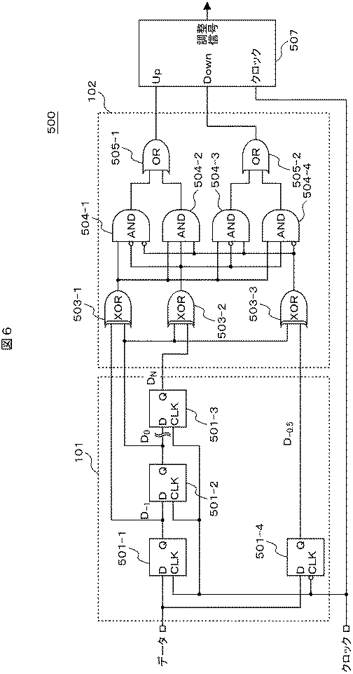
図6を参照して、波形等化量調整回路の具体的な構成を説明する。図6において、波形等化量調整回路500は、レシーバで受信したデータからデータDN、D0、D−1およびデータD−0.5を取得するデータ取得部101と、Up/Down信号を生成するデータパタン評価部102と、Up/Downカウント部103、取得データカウント部104、Up/Down信号差分評価部105の機能を持つ論理演算回路507とから構成される。
A specific configuration of the waveform equalization amount adjusting circuit will be described with reference to FIG. In FIG. 6, a waveform equalization
データ取得部101は、4つのフリップフロップ回路501で構成される。フリップフロップ回路501のそれぞれのデータ出力端子は、後段のデータパタン評価部102の入力端子に接続される。なお、フリップフロップ回路501−4へのクロックは、反転されているので、D−0.5を出力する。
The
Up/Down信号を生成するデータパタン評価部102は、3つの排他的論理和回路(XOR)、4つの論理積回路(AND)、2つの論理和回路(OR)で構成することができる。
The data
データ取得部101から出力されたデータD−1、D−0.5、D0、DNは、3つの排他的論理和回路503に入力される。排他的論理和回路503のそれぞれの出力端子は、後段の4つの論理積回路504のそれぞれの入力端子に接続される。さらに、論理積回路504のそれぞれの出力端子は論理和回路505のそれぞれの入力端子に接続される。論理和回路505のそれぞれの出力信号はUp/Down信号として、論理演算回路507へ出力される。
Data D-1, D-0.5, D0, and DN output from the
上述したような回路構成により、波形等化量調整回路を実現することができる。ここで示した回路構成は、一例であり、たとえば、取得したデータをレジスタに保存しておき、保存データをもとにソフトウェアで波形等化量を調整する方法でも、同様の効果を得る。 With the circuit configuration as described above, a waveform equalization amount adjusting circuit can be realized. The circuit configuration shown here is an example. For example, the same effect can be obtained by a method in which acquired data is stored in a register and the waveform equalization amount is adjusted by software based on the stored data.
図7を参照して、論理演算回路の具体的な構成を説明する。図7において、論理演算回路507は、Up/Downカウント部103と、取得データカウント部104と、Up/Down信号差分評価部105とから構成される。さらに、Up/Downカウント部103は、2つのカウンタ901で構成される。取得データカウント部104は、カウンタ901−3と比較器905−1とで構成される。Up/Down信号差分評価部105は、減算器907と比較器905−2とで構成される。
A specific configuration of the logical operation circuit will be described with reference to FIG. In FIG. 7, the
論理演算回路507は、入力されたUp信号、Down信号、およびクロック信号のそれぞれの数をカウンタ901でカウントする。ここで、クロック信号数は、取得データ数と等価であることを利用している。取得データカウント部104は、クロックカウンタ値と所定のしきい値Nを比較する。クロックカウンタ値がしきい値Nを超えた場合、比較器905−1は、減算器907の動作信号を出力する。減算器907は、動作信号を受信して、Upカウンタ値とDownカウンタ値を減算した差分信号を、後段の比較器905−2に出力する。比較器905−2は、差分信号と所定のしきい値Mとを比較する。比較器905−2は、絶対値がしきい値Mより大きく極性が正であれば、波形等化量を増やす方向に波形等化量調整信号を出力する。比較器905−2は、絶対値がしきい値Mより大きく極性が負であれば、波形等化量を減らす方向に波形等化量調整信号を出力する。比較器905−2は、絶対値がしきい値Mを超えていない場合には波形等化量を維持するように波形等化量調整信号を出力する。
The
上記のように論理演算回路を構成することにより、Up信号、Down信号およびクロック信号を用いて、波形等化量の過不足を判別して、その結果に応じた調整信号を出力することができる。 By configuring the logic operation circuit as described above, it is possible to determine whether the waveform equalization amount is excessive or insufficient using the Up signal, the Down signal, and the clock signal, and to output an adjustment signal according to the result. .
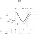
実施例2について、図8を参照して説明する。ここで、図8(a)は、受信データ波形を説明する図である。また、図8(b)は、CDRによる再生クロック波形である。実施例2では、データ取得部101において、CDRによる再生クロックで取得したデータDN、D0、D−1と、再生クロックから半データシンボルより短い位相分を遅延したクロックで取得したデータD−aと、再生クロックから半データシンボルより長い位相分を遅延したクロックで取得したデータD−bとを取得する。
A second embodiment will be described with reference to FIG. Here, FIG. 8A is a diagram for explaining a received data waveform. FIG. 8B shows a reproduction clock waveform by CDR. In the second embodiment, in the
実施例2によれば、再生クロックから半データシンボルより短い位相分を遅延したクロックと、再生クロックから半データシンボルより長い位相分を遅延したクロックとの間のタイミングでデータの符号が反転した場合にはUp/Down信号を出力しない。すなわち、Up/Down信号を出力しない不感タイミングを設けることができることから、波形等化量調整回路の動作を安定させることができる。 According to the second embodiment, when the sign of data is inverted at a timing between a clock delayed by a phase shorter than the half data symbol from the recovered clock and a clock delayed by a phase longer than the half data symbol from the recovered clock. Does not output an Up / Down signal. That is, since it is possible to provide a dead time at which no Up / Down signal is output, the operation of the waveform equalization amount adjusting circuit can be stabilized.
また、3相クロックを用いるCDR方式の場合には、データDN、D0、D−1、D−aおよびD−bとして、CDRのクロック再生動作に必要なデータと共通化することができることから、CDRに搭載される回路の一部を実施例2の波形等化調整回路に利用できる。 In the case of the CDR method using a three-phase clock, data DN, D0, D-1, Da, and Db can be shared with data necessary for CDR clock reproduction operation. A part of the circuit mounted on the CDR can be used for the waveform equalization adjustment circuit of the second embodiment.
他の実施の形態について、実施例3を図9を参照しながら、説明する。図9は、波形等化量調整回路を適用したLSIを搭載した情報ネットワーク装置の斜視図である。図9において、情報ネットワーク装置600は、データ伝送を行うインターフェースを持つLSI604と、LSI604を搭載する複数のドータボード602と、複数のドータボード602間に信号を伝送するためのバックプレーン601と、ドータボード602とバックプレーンを電気的に接続するバックプレーンコネクタ603とで構成される。特に、LSI604は、実施例1または実施例2の波形等化量調整回路を適用している。
Another embodiment will be described with reference to FIG. FIG. 9 is a perspective view of an information network device equipped with an LSI to which a waveform equalization amount adjusting circuit is applied. 9, the
上述のように装置を構成することにより、レシーバで受信したデータのみで波形等化量を最適化できるので、回路特性の経時変化などにより波形等化量の最適値が変動した場合でも、装置を通常動作させた状態で波形等化量を最適化でき、安定した動作を保障することができる。 By configuring the device as described above, the waveform equalization amount can be optimized only by the data received by the receiver, so even if the optimum value of the waveform equalization amount fluctuates due to changes in circuit characteristics over time, the device can be The amount of waveform equalization can be optimized in the state of normal operation, and stable operation can be ensured.
上述した実施例3によれば、回路特性などが経時変化や環境変動した場合でも装置を通常動作させたまま波形等化量を最適化できる。情報ネットワーク装置は、安定した動作が要求されるルータ、サーバ、PCを含みこれらに限られない。また、情報端末機器にも適用可能である。 According to the third embodiment described above, the amount of waveform equalization can be optimized while the apparatus is operating normally even when the circuit characteristics and the like change with time or the environment changes. Information network devices include, but are not limited to, routers, servers, and PCs that require stable operation. It can also be applied to information terminal equipment.
100…波形等化調整回路、101…データ取得部、102…データパタン評価部、103…Up/Down信号カウント部、104…取得データ数判定部、105…Up/Down信号差分評価部、201…LSI、202…ドライバ、203…レシーバ、204…論理回路、205…I/O回路、206…伝送路、207…伝送路、301…101パタン、302…001パタン、303…符号判定レベル、311…101パタン、312…001パタン、321…101パタン、322…001パタン、341…CDR再生クロック、401…101パタン、402…001パタン、403…符号判定レベル、404…CDR再生クロック、501…フリップフロップ回路、503…排他的論理和回路、504…論理積回路、505…論理和回路、507…論理演算回路、600…情報ネットワーク装置、601…バックプレーン、602…ドータボード、603…バックプレーンコネクタ、604…LSI、700…エンファシス回路、701…遅延回路、702…乗算器、703…加算器、800…波形等化調整回路、901…カウンタ、905…比較器、907…減算器。
DESCRIPTION OF
Claims (4)
受信データから再生されたクロックの第1のタイミングで第1のデータを取得するステップと、
前記第1のタイミングと1個のデータシンボル長遅れた第2のタイミングで第2のデータを取得するステップと、
前記第1のタイミングとN個のデータシンボル長早い第3のタイミングで第3のデータを取得するステップと、
前記第1のタイミングと半データシンボルより短い位相分を遅延した第4のタイミングで第4のデータを取得するステップと、
前記第1のタイミングと半データシンボルより長い位相分を遅延した第5のタイミングで第5のデータを取得するステップと、
取得した前記第1のデータないし前記第5のデータのデータセットのデータパタンを評価してUp信号とDown信号とを出力するステップと、
前記Up信号と前記Down信号との数をカウントするステップと、
前記データセットの数をカウントして所定のカウント数を満たしているかを評価するステップと、
カウントしたUp信号の数とDown信号の数との差分と所定の差分しきい値とを比較して波形等化量調整信号を出力するステップと、
を含み、
前記Up信号とDown信号とを出力するステップにおいて、前記第4のデータと、前記第5のデータとの間で符号が反転した場合、Up信号およびDown信号を出力しないことを特徴とする波形等化量調整方法。 A waveform equalization amount adjustment method of a waveform equalization circuit for correcting waveform distortion due to transmission loss,
Obtaining first data at a first timing of a clock recovered from received data;
Obtaining second data at a second timing delayed by one data symbol length with the first timing;
Acquiring third data at a first timing and a third timing that is N data symbols long earlier;
Obtaining fourth data at a fourth timing delayed by a phase shorter than the first timing and a half data symbol;
Obtaining fifth data at a fifth timing delayed by a phase longer than the first timing and a half data symbol;
Evaluating a data pattern of the acquired data set of the first data to the fifth data and outputting an Up signal and a Down signal;
Counting the number of the Up signal and the Down signal;
Counting the number of the data sets to evaluate whether a predetermined count number is satisfied;
Comparing the difference between the counted number of Up signals and the number of Down signals with a predetermined difference threshold value and outputting a waveform equalization amount adjustment signal;
Including
In the step of outputting the Up signal and the Down signal, if the sign is inverted between the fourth data and the fifth data, the Up signal and the Down signal are not output. Adjustment method.
前記データ取得部は、
前記受信データから再生されたクロックの第1のタイミングで第1のデータを取得し、
前記第1のタイミングと1個のデータシンボル長遅れた第2のタイミングで第2のデータを取得し、
前記第1のタイミングとN個のデータシンボル長早い第3のタイミングで第3のデータを取得し、
前記第1のタイミングと半データシンボルより短い位相分を遅延した第4のタイミングで第4のデータを取得し、
前記第1のタイミングと半データシンボルより長い位相分を遅延した第5のタイミングで第5のデータを取得し、
前記データパタン評価部は、前記第4のデータと前記第5のデータとの間で符号が反転した場合、Up信号およびDown信号を出力しないことを特徴とする波形等化量調整回路。 A data acquisition unit that acquires data for adjusting a waveform equalization amount related to received data; a data pattern evaluation unit that evaluates a data pattern of the acquired data and outputs an Up signal and a Down signal; and the Up An Up / Down signal count unit that counts the number of signals and the Down signal, and an acquired data number determination unit that counts the number of data acquired by the data acquisition unit and evaluates whether a predetermined count number is satisfied. An Up / Down signal difference evaluation unit that compares a difference between the counted number of Up signals and the number of Down signals and a predetermined difference threshold value and outputs a waveform equalization amount adjustment signal. ,
The data acquisition unit
Obtaining first data at a first timing of a clock regenerated from the received data;
Acquiring second data at a second timing delayed by one data symbol length with the first timing;
Acquiring the third data at the first timing and the third timing that is N data symbols long earlier;
Acquiring the fourth data at a fourth timing delayed by a phase shorter than the first timing and a half data symbol;
Fifth data is acquired at a first timing and a fifth timing delayed by a phase longer than a half data symbol ;
The waveform equalization amount adjustment circuit, wherein the data pattern evaluation unit does not output an Up signal and a Down signal when a sign is inverted between the fourth data and the fifth data.
受信データに係る波形等化量を調整するためのデータを取得するデータ取得部と、取得した前記データのデータパタンを評価してUp信号とDown信号とを出力するデータパタン評価部と、前記Up信号と前記Down信号との数をカウントするUp/Down信号カウント部と、前記データ取得部で取得したデータの数をカウントして所定のカウント数を満たしているかを評価する取得データ数判定部と、カウントしたUp信号の数とDown信号の数との差分と所定の差分しきい値とを比較して波形等化量調整信号を出力するUp/Down信号差分評価部と、を含んで構成され、
前記データ取得部は、
前記受信データから再生されたクロックの第1のタイミングで第1のデータを取得し、
前記第1のタイミングと1個のデータシンボル長遅れた第2のタイミングで第2のデータを取得し、
前記第1のタイミングとN個のデータシンボル長早い第3のタイミングで第3のデータを取得し、
前記第1のタイミングと半データシンボルより短い位相分を遅延した第4のタイミングで第4のデータを取得し、
前記第1のタイミングと半データシンボルより長い位相分を遅延した第5のタイミングで第5のデータを取得し、
前記データパタン評価部は、前記第4のデータと前記第5のデータとの間で符号が反転した場合、Up信号およびDown信号を出力しない波形等化量調整回路を備えたことを特徴とする半導体装置。 In a semiconductor device equipped with a communication interface,
A data acquisition unit that acquires data for adjusting a waveform equalization amount related to received data; a data pattern evaluation unit that evaluates a data pattern of the acquired data and outputs an Up signal and a Down signal; and the Up An Up / Down signal count unit that counts the number of signals and the Down signal, and an acquired data number determination unit that counts the number of data acquired by the data acquisition unit and evaluates whether a predetermined count number is satisfied. An Up / Down signal difference evaluation unit that compares a difference between the counted number of Up signals and the number of Down signals and a predetermined difference threshold value and outputs a waveform equalization amount adjustment signal. ,
The data acquisition unit
Obtaining first data at a first timing of a clock regenerated from the received data;
Acquiring second data at a second timing delayed by one data symbol length with the first timing;
Acquiring the third data at the first timing and the third timing that is N data symbols long earlier;
Acquiring the fourth data at a fourth timing delayed by a phase shorter than the first timing and a half data symbol;
Fifth data is acquired at a first timing and a fifth timing delayed by a phase longer than a half data symbol ;
The data pattern evaluation unit includes a waveform equalization amount adjustment circuit that does not output an Up signal and a Down signal when a sign is inverted between the fourth data and the fifth data. Semiconductor device.
前記半導体装置は、受信データに係る波形等化量を調整するためのデータを取得するデータ取得部と、取得した前記データのデータパタンを評価してUp信号とDown信号とを出力するデータパタン評価部と、前記Up信号と前記Down信号との数をカウントするUp/Down信号カウント部と、前記データ取得部で取得したデータの数をカウントして所定のカウント数を満たしているかを評価する取得データ数判定部と、カウントしたUp信号の数とDown信号の数との差分と所定の差分しきい値とを比較して波形等化量調整信号を出力するUp/Down信号差分評価部と、を含んで構成され、
前記データ取得部は、
前記受信データから再生されたクロックの第1のタイミングで第1のデータを取得し、
前記第1のタイミングと1個のデータシンボル長遅れた第2のタイミングで第2のデータを取得し、
前記第1のタイミングとN個のデータシンボル長早い第3のタイミングで第3のデータを取得し、
前記第1のタイミングと半データシンボルより短い位相分を遅延した第4のタイミングで第4のデータを取得し、
前記第1のタイミングと半データシンボルより長い位相分を遅延した第5のタイミングで第5のデータを取得し、
前記データパタン評価部は、前記第4のデータと前記第5のデータとの間で符号が反転した場合、Up信号およびDown信号を出力しない波形等化量調整回路を備えたことを特徴とする情報ネットワーク装置。 In an information network device including first and second mounting substrates on which a semiconductor device having a communication interface is mounted, and a backplane substrate to which the first mounting substrate and the second mounting substrate are connected,
The semiconductor device includes a data acquisition unit that acquires data for adjusting a waveform equalization amount related to received data, and a data pattern evaluation that evaluates a data pattern of the acquired data and outputs an Up signal and a Down signal And an Up / Down signal counting unit that counts the number of the Up signal and the Down signal, and an acquisition that counts the number of data acquired by the data acquisition unit and evaluates whether a predetermined count number is satisfied A data number determination unit, an Up / Down signal difference evaluation unit that compares a difference between the counted number of Up signals and the number of Down signals and a predetermined difference threshold value and outputs a waveform equalization amount adjustment signal; Comprising
The data acquisition unit
Obtaining first data at a first timing of a clock regenerated from the received data;
Acquiring second data at a second timing delayed by one data symbol length with the first timing;
Acquiring the third data at the first timing and the third timing that is N data symbols long earlier;
Acquiring the fourth data at a fourth timing delayed by a phase shorter than the first timing and a half data symbol;
Fifth data is acquired at a first timing and a fifth timing delayed by a phase longer than a half data symbol ;
The data pattern evaluation unit includes a waveform equalization amount adjustment circuit that does not output an Up signal and a Down signal when a sign is inverted between the fourth data and the fifth data. Information network equipment.
Priority Applications (1)
| Application Number | Priority Date | Filing Date | Title |
|---|---|---|---|
| JP2008267825A JP5259333B2 (en) | 2008-10-16 | 2008-10-16 | Waveform equalization amount adjustment method, waveform equalization amount adjustment circuit, semiconductor device, and information network device |
Applications Claiming Priority (1)
| Application Number | Priority Date | Filing Date | Title |
|---|---|---|---|
| JP2008267825A JP5259333B2 (en) | 2008-10-16 | 2008-10-16 | Waveform equalization amount adjustment method, waveform equalization amount adjustment circuit, semiconductor device, and information network device |
Publications (2)
| Publication Number | Publication Date |
|---|---|
| JP2010098532A JP2010098532A (en) | 2010-04-30 |
| JP5259333B2 true JP5259333B2 (en) | 2013-08-07 |
Family
ID=42259906
Family Applications (1)
| Application Number | Title | Priority Date | Filing Date |
|---|---|---|---|
| JP2008267825A Expired - Fee Related JP5259333B2 (en) | 2008-10-16 | 2008-10-16 | Waveform equalization amount adjustment method, waveform equalization amount adjustment circuit, semiconductor device, and information network device |
Country Status (1)
| Country | Link |
|---|---|
| JP (1) | JP5259333B2 (en) |
Family Cites Families (3)
| Publication number | Priority date | Publication date | Assignee | Title |
|---|---|---|---|---|
| JP4331641B2 (en) * | 2004-04-09 | 2009-09-16 | 富士通株式会社 | Receiver circuit having equalization circuit |
| US7804894B2 (en) * | 2006-05-30 | 2010-09-28 | Fujitsu Limited | System and method for the adjustment of compensation applied to a signal using filter patterns |
| JP5540472B2 (en) * | 2008-06-06 | 2014-07-02 | ソニー株式会社 | Serial data receiver, gain control circuit, and gain control method |
-
2008
- 2008-10-16 JP JP2008267825A patent/JP5259333B2/en not_active Expired - Fee Related
Also Published As
| Publication number | Publication date |
|---|---|
| JP2010098532A (en) | 2010-04-30 |
Similar Documents
| Publication | Publication Date | Title |
|---|---|---|
| US8108710B2 (en) | Differential communication link with skew compensation circuit | |
| US7227375B2 (en) | DAC based driver with selectable pre-emphasis signal levels | |
| TWI564720B (en) | Unequalized clock data recovery for serial i/o receiver | |
| US20090121761A1 (en) | Intra-pair differential skew compensation method and apparatus for high-speed cable data transmission systems | |
| WO2009113462A1 (en) | Waveform equalization circuit and waveform equalization method | |
| KR102938433B1 (en) | Bit-level mode retimer | |
| US8929429B2 (en) | Adaptive pade filter and transceiver | |
| JP2010226406A (en) | Transmission equipment | |
| US7924912B1 (en) | Method and apparatus for a unified signaling decision feedback equalizer | |
| US11936505B2 (en) | Decision feedback equalization with efficient burst error correction | |
| US20120014460A1 (en) | Compensation for Transmission Line Length Variation in a Serdes System | |
| US7965765B2 (en) | Adjustment method, circuit, receiver circuit and transmission equipment of waveform equalization coefficient | |
| JP5259333B2 (en) | Waveform equalization amount adjustment method, waveform equalization amount adjustment circuit, semiconductor device, and information network device | |
| US7426235B1 (en) | Method of adaptive equalization for high-speed NRZ and multi-level signal data communications | |
| US7590176B2 (en) | Partial response transmission system and equalizing circuit thereof | |
| US12519680B2 (en) | Receiver and method for controlling equalization | |
| CN104579618A (en) | Method applied to interconnection system and related processing module | |
| JP2014033347A (en) | Adaptive equalizer, equalizer adjustment method, semiconductor device using the same and information network device | |
| CN119449544A (en) | Receiver and method with fast sampling phase and frequency acquisition | |
| US7529296B2 (en) | Adaptive equalization method and circuit for continuous run-time adaptation | |
| US20140043097A1 (en) | Electronic device and noise reducing method | |
| TWI416920B (en) | Slicing level and sampling phase adaptation circuitry for data recovery systems | |
| Healey | Challenges and solutions for standards-based serial 10 Gb/s backplane Ethernet | |
| US7154972B2 (en) | Receiver-side adaptive equalization in source-synchronous chip-to-chip communication systems | |
| JP2012039229A (en) | Receiving device |
Legal Events
| Date | Code | Title | Description |
|---|---|---|---|
| A621 | Written request for application examination |
Free format text: JAPANESE INTERMEDIATE CODE: A621 Effective date: 20101220 |
|
| A977 | Report on retrieval |
Free format text: JAPANESE INTERMEDIATE CODE: A971007 Effective date: 20120525 |
|
| A131 | Notification of reasons for refusal |
Free format text: JAPANESE INTERMEDIATE CODE: A131 Effective date: 20120605 |
|
| A521 | Written amendment |
Free format text: JAPANESE INTERMEDIATE CODE: A523 Effective date: 20120730 |
|
| A131 | Notification of reasons for refusal |
Free format text: JAPANESE INTERMEDIATE CODE: A131 Effective date: 20121113 |
|
| A521 | Written amendment |
Free format text: JAPANESE INTERMEDIATE CODE: A523 Effective date: 20130109 |
|
| TRDD | Decision of grant or rejection written | ||
| A01 | Written decision to grant a patent or to grant a registration (utility model) |
Free format text: JAPANESE INTERMEDIATE CODE: A01 Effective date: 20130409 |
|
| A61 | First payment of annual fees (during grant procedure) |
Free format text: JAPANESE INTERMEDIATE CODE: A61 Effective date: 20130424 |
|
| FPAY | Renewal fee payment (event date is renewal date of database) |
Free format text: PAYMENT UNTIL: 20160502 Year of fee payment: 3 |
|
| R150 | Certificate of patent or registration of utility model |
Free format text: JAPANESE INTERMEDIATE CODE: R150 |
|
| LAPS | Cancellation because of no payment of annual fees |