JP5259173B2 - Light modulator - Google Patents
Light modulator Download PDFInfo
- Publication number
- JP5259173B2 JP5259173B2 JP2007329036A JP2007329036A JP5259173B2 JP 5259173 B2 JP5259173 B2 JP 5259173B2 JP 2007329036 A JP2007329036 A JP 2007329036A JP 2007329036 A JP2007329036 A JP 2007329036A JP 5259173 B2 JP5259173 B2 JP 5259173B2
- Authority
- JP
- Japan
- Prior art keywords
- characteristic impedance
- impedance
- ghz
- optical modulator
- interaction
- Prior art date
- Legal status (The legal status is an assumption and is not a legal conclusion. Google has not performed a legal analysis and makes no representation as to the accuracy of the status listed.)
- Expired - Fee Related
Links
Images


Landscapes
- Optical Modulation, Optical Deflection, Nonlinear Optics, Optical Demodulation, Optical Logic Elements (AREA)
Description
本発明は駆動電圧が低く、かつ高速で変調が可能な光変調器の分野に属する。 The present invention belongs to the field of optical modulators having a low driving voltage and capable of high-speed modulation.
リチウムナイオベート(LiNbO3)のように電界を印加することにより屈折率が変化する、いわゆる電気光学効果を有する基板(以下、リチウムナイオベート基板をLN基板と略す)に光導波路と進行波電極を形成した進行波電極型リチウムナイオベート光変調器(以下、LN光変調器と略す)は、その優れたチャーピング特性から2.5Gbit/s、10Gbit/sの大容量光伝送システムに適用されている。最近はさらに40Gbit/sの超大容量光伝送システムにも適用が検討されており、キーデバイスとして期待されている。 An optical waveguide and a traveling wave electrode are provided on a substrate having a so-called electro-optic effect (hereinafter, the lithium niobate substrate is abbreviated as an LN substrate) such as lithium niobate (LiNbO 3 ) whose refractive index is changed by applying an electric field. The formed traveling-wave electrode type lithium niobate optical modulator (hereinafter abbreviated as LN optical modulator) is applied to a 2.5 Gbit / s, 10 Gbit / s large capacity optical transmission system because of its excellent chirping characteristics. Yes. Recently, application to an ultra large capacity optical transmission system of 40 Gbit / s is also being studied, and it is expected as a key device.
[第1の従来技術]
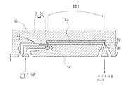
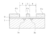
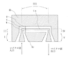
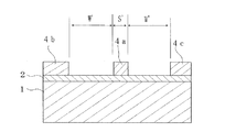
このLN光変調器にはz−カット基板を使用するタイプとx−カット基板(あるいはy−カット基板)を使用するタイプがある。ここでは、第1の従来技術としてx−カットLN基板とコプレーナウェーブガイド(CPW)進行波電極を使用したx−カット基板LN光変調器をとり上げ、その斜視図を図10に示す。図11は図10のA−A’における断面図である。なお、以下の議論はz−カット基板でも同様に成り立つ。
[First prior art]
This LN optical modulator includes a type using a z-cut substrate and a type using an x-cut substrate (or y-cut substrate). Here, an x-cut substrate LN optical modulator using an x-cut LN substrate and a coplanar waveguide (CPW) traveling wave electrode is taken up as a first prior art, and a perspective view thereof is shown in FIG. FIG. 11 is a cross-sectional view taken along line AA ′ of FIG. The following discussion holds true for z-cut substrates as well.
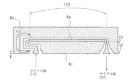
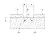
図中、1はx−カットLN基板、2は1.3μm、あるいは1.55μmなど光通信において使用する波長領域では透明な200nmから1μm程度の厚みのSiO2バッファ層、3はx−カットLN基板1にTiを蒸着後、1050℃で約10時間熱拡散して形成した光導波路であり、光は光入射用端面30から光導波路3に入射させる。なお、この光導波路3はマッハツェンダ干渉系(あるいは、マッハツェンダ光導波路)を構成しており、3a、3bは電気信号と光が相互作用する部位(相互作用部と言う)における光導波路(あるいは、相互作用光導波路)、つまりマッハツェンダ光導波路の2本のアームである。CPW進行波電極4は中心導体4a、接地導体4b、4cからなっている。また、図11においてSは中心導体4aの幅で6μmから20μm程度であり、一般には10μm前後が使用されている。一方、Wは中心導体4aと接地導体4b、4cの間のギャップ(あるいはCPWのギャップ)である。
In the figure, 1 is an x-cut LN substrate, 2 is a transparent SiO 2 buffer layer having a thickness of about 200 nm to 1 μm in the wavelength region used in optical communication such as 1.3 μm or 1.55 μm, and 3 is an x-cut LN. The optical waveguide is formed by thermally diffusing Ti at 1050 ° C. for about 10 hours after Ti is deposited on the
この第1の従来技術では、中心導体4aと接地導体4b、4c間にバイアス電圧(通常はDCバイアス電圧)と高周波電気信号(マイクロ波、あるいはRF電気信号とも言う)を重畳して印加する。また、SiO2バッファ層2は高周波電気信号の等価屈折率nm(あるいは、マイクロ波等価屈折率nm)を相互作用光導波路3a、3bを伝搬する光の実効屈折率noに近づけることにより、光変調帯域を拡大するという重要な働きをしている。
In the first prior art, a bias voltage (usually a DC bias voltage) and a high-frequency electric signal (also referred to as a microwave or an RF electric signal) are superimposed and applied between the
次に、このように構成されるLN光変調器の動作について説明する。このLN光変調器を動作させるには、中心導体4aと接地導体4b、4c間にDCバイアス電圧と高周波電気信号とを印加する必要がある。
Next, the operation of the LN optical modulator configured as described above will be described. In order to operate this LN optical modulator, it is necessary to apply a DC bias voltage and a high-frequency electric signal between the
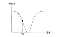
図12に示す電圧−光出力特性はある状態でのLN光変調器の電圧−光出力特性であり、Vbはその際のDCバイアス電圧である。この図12に示すように、通常、DCバイアス電圧Vbは光出力特性の山と底の中点に設定される。 The voltage-light output characteristic shown in FIG. 12 is the voltage-light output characteristic of the LN optical modulator in a certain state, and Vb is the DC bias voltage at that time. As shown in FIG. 12, the DC bias voltage Vb is normally set at the midpoint between the peak and bottom of the light output characteristic.
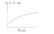
図13には半波長電圧Vπと相互作用部の長さLとの積Vπ・LとCPWのギャップWとの関係を示す。なお、CPWのギャップWとしては、現状20μm〜30μm程度が使用されている。CPWのギャップWを狭くすると、相互作用光導波路3a、3bを伝搬する光と相互作用する高周波電界強度が大きくなる。従って、この図に示すように、CPWのギャップWを狭くすると、この積Vπ・Lは小さくなる。そして、この積Vπ・Lが低いほど駆動電圧が低いLN光変調器を実現できる。10Gbps以上の速度でLN光変調器を駆動する際の駆動電圧は5〜6V程度が実用上の限界であり、さらに少しでも駆動電圧が低いことが望まれる。よって駆動電圧の観点からは、CPWのギャップWは狭いことが望ましい。
FIG. 13 shows the relationship between the product Vπ · L of the half-wave voltage Vπ and the length L of the interaction portion and the gap W of the CPW. In addition, as the gap W of CPW, about 20-30 micrometers is used now. When the gap W of the CPW is narrowed, the strength of the high frequency electric field that interacts with the light propagating through the interaction
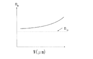
図14には高周波電気信号のマイクロ波の等価屈折率nmとCPWのギャップWとの関係を示す。図には相互作用光導波路3a、3bを伝搬する光の等価屈折率no(no≒2.2)も示している。
It shows the relationship between the microwave equivalent refractive index n m and CPW gaps W high-frequency electric signal in FIG. It shows the interaction
CPWのギャップWが狭くなると中心導体4aと接地導体4b、4cの間に生成された高周波電気信号は比誘電率が4程度と低いSiO2バッファ層2を多く感じるので、マイクロ波等価屈折率nmを低減することができる(なお、x−カットLN基板1の比誘電率は35程度である)。
When the gap W of the CPW is narrowed, the high frequency electric signal generated between the
一般に、マイクロ波等価屈折率nmは光の等価屈折率noよりも大きく、LN光変調器を高速・広帯域で動作する際の大きな制限要因となっている。そのためLN光変調器を10Gbps以上の高速で駆動するには、マイクロ波等価屈折率nmを光の等価屈折率noに近づけることが不可欠となる。この観点からもCPWのギャップWは狭いことが望ましい。 In general, the microwave equivalent refractive index n m is greater than the equivalent refractive index n o of the light, is a major limiting factor in the operation of the LN optical modulator at a high speed and a wide band. Therefore, to drive the LN optical modulator in faster than 10Gbps becomes essential to close the microwave equivalent refractive index n m in the light of the equivalent refractive index n o. From this point of view, it is desirable that the gap W of the CPW is narrow.
以上のように、駆動電圧を低減するとともにマイクロ波等価屈折率nmを光の等価屈折率noに近づけるという観点からはCPWのギャップWは狭いことが望ましいことがわかったが、第1の従来技術においてCPWのギャップWを15μm以下に狭くした際に生じる問題点について以下に記す。 As described above, while reducing the driving voltage of the CPW gap W from the viewpoint closer to the microwave equivalent refractive index n m in the light of the equivalent refractive index n o has been found to be narrow it is desirable, first The problems that occur when the CPW gap W is narrowed to 15 μm or less in the prior art will be described below.
図15は中心導体4aと接地導体4b、4cからなるCPW進行波電極4の特性インピーダンスZ(以下の図17におけるZ3に対応)についてCPWギャップWを変数として示す。CPWギャップWを狭くすると、特性インピーダンスZが30Ωあるいはそれ以下と著しく低くなり、ほぼ50Ω系の外部信号源との間にインピーダンス不整合を生じてしまう。つまり、高周波電気信号のパワー反射率(いわゆるS11)が劣化するという問題が生じる。
Figure 15 shows the CPW gaps W as a variable for the
次に、このことについてさらに詳しく考察する。図10に示したx−カット基板LN光変調器を構成する中心導体4aと接地導体4b、4cからなるCPW進行波電極4の上面図を図16に示す。
Next, this will be considered in more detail. FIG. 16 shows a top view of the CPW
ここで、Iは不図示の外部信号源からの高周波電気信号をCPW進行波電極4に印加するための不図示のコネクタの芯線(あるいは金リボンや金ワイヤー)を接続する入力用フィードスルー部、IIは入力用フィードスルー部Iと相互作用部IIIとの接続部(あるいは入力側接続部)、IIIは電気信号と光が相互作用する相互作用部、IVは出力用フィードスルー部Vと相互作用部IIIとの接続部(あるいは出力側接続部)である。出力用フィードスルー部Vは不図示のコネクタの芯線(あるいは金リボンや金ワイヤー)もしくは終端抵抗に接続される。
Here, I is an input feed-through unit for connecting a core wire (or a gold ribbon or a gold wire) of a connector (not shown) for applying a high-frequency electrical signal from an external signal source (not shown) to the CPW
なお、入力用フィードスルー部Iの中心導体において高周波電気信号を給電する部位を給電部とし、また、出力用フィードスルーの中心導体において高周波電気信号を取り出す部位を出力部と呼ぶ。 A portion that feeds a high-frequency electrical signal in the central conductor of the input feedthrough portion I is referred to as a feeding portion, and a portion that takes out the high-frequency electrical signal in the central conductor of the output feedthrough is referred to as an output portion.
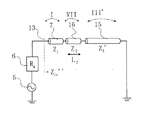
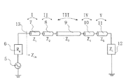
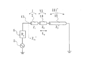
図17には図10に示したx−カット基板LN光変調器の等価回路を示す。ここで、5と6は外部回路に対応し、5は電気的ドライバなどの外部信号源、6は外部信号源の特性インピーダンスRg(あるいは、負荷抵抗、出力インピーダンス、インピーダンスと呼ばれる)を表す。また、7〜11は入力用フィードスルー部Iから出力用フィードスルー部Vまでの等価的な線路に各々対応する。具体的には、7は入力用フィードスルー部I、8は入力側接続部II、9は相互作用部III、10は出力側接続部IV、11は出力用フィードスルー部Vの線路を各々表す。また、12は終端抵抗である。
FIG. 17 shows an equivalent circuit of the x-cut substrate LN optical modulator shown in FIG. Here, 5 and 6 correspond to external circuits, 5 represents an external signal source such as an electric driver, and 6 represents a characteristic impedance R g (also referred to as load resistance, output impedance, or impedance) of the external signal source. Reference numerals 7 to 11 respectively correspond to equivalent lines from the input feedthrough portion I to the output feedthrough portion V. Specifically, 7 is an input feedthrough section I, 8 is an input side connection section II, 9 is an interaction section III, 10 is an output side connection section IV, and 11 is a line of an output feedthrough section V. .
さらに、Z1〜Z5は入力用フィードスルー部Iから出力用フィードスルー部Vまでの特性インピーダンスであり、具体的には、Z1は入力用フィードスルー部I(あるいは線路7)、Z2は入力側接続部II(あるいは線路8)、Z3は相互作用部III(あるいは線路9)、Z4は出力側接続部IV(あるいは線路10)、Z5は出力用フィードスルー部V(あるいは線路11)の特性インピーダンスに対応している。また、ZLは終端抵抗12の抵抗値である。
Further, Z 1 to Z 5 are characteristic impedances from the input feed-through portion I to the output feed-through portion V. Specifically, Z 1 is the input feed-through portion I (or line 7), Z 2. an input-side connecting portion II (or the line 8), Z 3 is the interaction portion III (or the line 9), Z 4 is output connection portion IV (or the line 10), Z 5 is output feed-through portion V (or This corresponds to the characteristic impedance of the line 11). Z L is the resistance value of the
次に、図10から図17に示した第1の従来技術のx−カット基板LN光変調器について、インピーダンス不整合と変調帯域の観点からの問題点について考察する。 Next, problems in terms of impedance mismatch and modulation band will be considered for the first conventional x-cut substrate LN optical modulator shown in FIGS.
図17において、Zinは外部信号源5とRgである負荷抵抗6(あるいは、出力インピーダンス、特性インピーダンス、あるいはインピーダンスをとする)からx−カット基板LN光変調器を見た入力インピーダンスとなる。つまり、Zinは入力用フィードスルー部Iの特性インピーダンスZ1、入力側接続部IIの特性インピーダンスZ2、相互作用部IIIの特性インピーダンスZ3、出力側接続部IVの特性インピーダンスZ4、出力用フィードスルー部Vの特性インピーダンスZ5、及び終端抵抗12の抵抗値ZLを、各部の長さと各部を伝搬する電気信号の等価屈折率を考慮した伝送線路の縦続接続の考え方で合成した特性インピーダンスと言える。図中の13は外部信号源5や負荷抵抗6と入力用フィードスルー部Iとの境界を表す。
In FIG. 17, Z in is an input impedance when the x-cut substrate LN optical modulator is viewed from the
駆動電圧を下げ、マイクロ波等価屈折率nmを光の等価屈折率noに近づけるためにCPWギャップWを15μm以下と狭くした場合を考察する。この場合、相互作用部IIIの特性インピーダンスZ3は30Ωあるいはそれ以下と低くなる。 Lowering the driving voltage, consider the case where the CPW gaps W in order to close the microwave equivalent refractive index n m for the light of the equivalent refractive index n o and narrow as 15μm or less. In this case, the characteristic impedance Z 3 of the interaction portion III is as low as 30Ω or less.
さて、第1の従来技術では、その他の線路7、8、10、11の特性インピーダンス、つまり入力用フィードスルー部Iの特性インピーダンスZ1、入力側接続部IIの特性インピーダンスZ2、出力側接続部IVの特性インピーダンスZ4、出力用フィードスルー部Vの特性インピーダンスZ5、及び終端抵抗12の抵抗値ZLは全て相互作用部IIIの特性インピーダンスZ3と等しくしていた(つまり、Z1=Z2=Z3=Z4=Z5=ZL)。
Now, the first conventional art, the characteristic impedance of
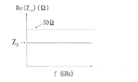
その結果、外部信号源5の負荷抵抗6からx−カット基板LN光変調器を見た入力インピーダンスZinの実部Re(Zin)は図18の実線で示すようにほとんど周波数fに依存せず、相互作用部IIIの特性インピーダンスZ3と一致し、30Ωもしくはそれ以下と低かった。
As a result, the real part Re (Z in ) of the input impedance Z in when the x-cut substrate LN optical modulator is viewed from the
それに伴い、光の変調指数(パワー変調指数)|m|2は入力インピーダンスZinと外部信号源5の負荷抵抗6の特性インピーダンスRg(あるいは負荷抵抗、出力インピーダンス、あるいはインピーダンス)とのインピーダンス不整合のために、図19に示すように、周波数fとともに急速に劣化し3dB光変調帯域として10GHzを確保することが極めて困難であった。
Accordingly, the optical modulation index (power modulation index) | m | 2 is an impedance difference between the input impedance Z in and the characteristic impedance R g (or load resistance, output impedance, or impedance) of the
なお、Z1=Z2=Z3=Z4=Z5=ZLと仮定すると、Zin(この場合には、Zin=Z3)が30Ωになると高周波電気信号のパワー反射率(S11)は図20に示すように約−12dBと高く(悪く)なってしまう。ここで、高周波電気信号のパワー反射率(S11)は次の式で与えられる。
S11=|(Rg−Zin)/(Rg+Zin)|2 (1)
また、反射された高周波電気信号は外部信号源5へ戻り、外部信号源5から出力される電気信号に重畳されるので、変調された光パルスのジッタ2psを越えてしまう。このように光パルスのジッタが増加すると実際の光伝送において誤り率が高く(悪く)なるので、光パルスのジッタとしては2ps以下と小さくすることが望ましい。
Assuming that Z 1 = Z 2 = Z 3 = Z 4 = Z 5 = Z L , when Z in (in this case, Z in = Z 3 ) becomes 30Ω, the power reflectivity (S 11 ) becomes high (bad) as about -12 dB as shown in FIG. Here, the power reflectivity (S 11 ) of the high-frequency electrical signal is given by the following equation.
S 11 = | (R g −Z in ) / (R g + Z in ) | 2 (1)
Further, since the reflected high-frequency electric signal returns to the
[第2の従来技術]
第1の従来技術における外部信号源5の特性インピーダンスRgと相互作用部IIIの特性インピーダンスZ3とのインピーダンス不整合を改善するための技術として、以下において特許文献1に提案された第2の従来技術について説明する。ここで、図10から図20に示した第1の従来技術と同一番号は同一機能部に対応しているため、ここでは同一番号を持つ機能部の説明を省略する。
[Second prior art]
As a technique for improving the impedance mismatch between the characteristic impedance R g and the interaction portion III characteristic impedance Z 3 of the
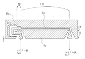
図21に第2の従来技術に使用するCPW進行波電極4の上面図を示す。第2の従来技術においても第1の従来技術と同様に、Iは入力用フィードスルー部、IIは入力側接続部、IIIは相互作用部、IVは出力側接続部、及びVは出力用フィードスルー部である。出力用フィードスルー部Vは不図示のコネクタ芯線(あるいは金リボンや金ワイヤー)もしくは終端抵抗に接続されるのも同じである。これらの第1の従来技術と同じ構成に加えて、図21に示す第2の従来技術には長さL6のインピーダンス変換部VIが付加されている。
FIG. 21 shows a top view of the CPW
図21の相互作用部IIIのB−B’におけるx−カット基板LN光変調器としての断面図を図22に示す。図11に示した第1の従来技術と同様に、図22に示す第2の従来技術でもCPWのギャップWを15μm程度以下と極めて狭く設定した場合を想定する。CPWのギャップWをこのように狭くすると、前述のように駆動電圧を低減できるとともに高周波電気信号のマイクロ波等価屈折率nmを相互作用光導波路3a、3bを伝搬する光の等価屈折率noに近づけることができるという利点はあるものの、相互作用部IIIの特性インピーダンスZ3は30Ωかそれ以下となる。
FIG. 22 shows a cross-sectional view as an x-cut substrate LN optical modulator at BB ′ of the interaction part III in FIG. Similar to the first prior art shown in FIG. 11, a case is assumed in which the gap W of the CPW is set to be as narrow as about 15 μm or less in the second prior art shown in FIG. If the gap W of CPW thus narrow, microwave equivalent refractive index n m of the interaction
またインピーダンス変換部VIのC−C’におけるx−カット基板LN光変調器としての断面図を図23に示す。インピーダンス変換部VIにおけるCPWのギャップW’は50μm程度と相互作用部IIIにおけるCPWのギャップWよりも広く設定される。 FIG. 23 shows a cross-sectional view of the impedance conversion unit VI as an x-cut substrate LN optical modulator at C-C ′. The CPW gap W ′ in the impedance conversion unit VI is set to be about 50 μm, which is wider than the CPW gap W in the interaction unit III.
図24には第2の従来技術の等価回路を示す。図17に示した第1の従来技術と同じく、Z1は入力用フィードスルー部I(あるいは線路7)、Z2は入力側接続部II(あるいは線路8)、Z3は相互作用部III(あるいは線路9)、Z4は出力側接続部IV(あるいは線路10)、Z5は出力用フィードスルー部V(あるいは線路11)の特性インピーダンスであるが、第2の従来技術には特性インピーダンスZ6のインピーダンス変換部VI(あるいは線路14)が付加されている。 FIG. 24 shows an equivalent circuit of the second prior art. As in the first prior art shown in FIG. 17, Z 1 is an input feed-through part I (or line 7), Z 2 is an input side connection part II (or line 8), and Z 3 is an interaction part III ( or the line 9), Z 4 is output connection portion IV (or the line 10), although Z 5 is a characteristic impedance of the output feed-through portion V (or the line 11), the second prior art characteristic impedance Z 6 impedance converters VI (or lines 14) are added.
図24中の13は外部信号源5の負荷抵抗6(出力インピーダンス、特性インピーダンス、あるいはインピーダンスをRgとする)と入力用フィードスルー部Iとの境界を表す。図24においてZin’は外部信号源5と外部信号源5の負荷抵抗6から第2の従来技術のx−カット基板LN光変調器を見た入力インピーダンスである。
In FIG. 24, 13 represents the boundary between the load resistor 6 (output impedance, characteristic impedance, or impedance is Rg ) of the
つまり、Zin’は入力用フィードスルー部Iの特性インピーダンスZ1、インピーダンス変換部VIの特性インピーダンスZ6、入力側接続部IIの特性インピーダンスZ2、相互作用部IIIの特性インピーダンスZ3、出力側接続部IVの特性インピーダンスZ4、出力用フィードスルー部Vの特性インピーダンスZ5、及び終端抵抗12の抵抗値ZLを伝送線路の縦続接続の考え方で合成した特性インピーダンスと言える。
That, Z in 'the characteristic impedance Z 1 of the input feed-through portion I, the characteristic impedance Z 6 of the impedance conversion section VI, the characteristic impedance Z 2 of the input-side connecting portion II, the interaction portion III of the characteristic impedance Z 3, the output the characteristic impedance of the side connecting portion IV Z 4, it said synthesized characteristic impedance in the concept of cascaded transmission line resistance Z L of the output feed-through portion characteristic impedance Z 5 of V, and the terminating
前述のように、第2の従来技術においてはCPWギャップWを15μm以下と狭くしたので、相互作用部IIIの特性インピーダンスZ3は30Ωあるいはそれ以下と低くなっている。 As described above, since the CPW gap W is narrowed to 15 μm or less in the second prior art, the characteristic impedance Z 3 of the interaction part III is as low as 30Ω or less.
次に、インピーダンス変換部VIの作用について考察する。簡単のために、入力側接続部IIの特性インピーダンスZ2、相互作用部IIIの特性インピーダンスZ3、出力側接続部IVの特性インピーダンスZ4、出力用フィードスルー部Vの特性インピーダンスZ5、及び終端抵抗12のZLについて、Z2=Z3=Z4=Z5=ZLが成り立っているとする。但し、入力側接続部IIと出力側接続部IVはそれらの長さが短いので、特性インピーダンスZ2、Z4が合成部III’の特性インピーダンスZ3’に与える影響は小さい。
Next, the operation of the impedance converter VI will be considered. For simplicity, the input-side connecting portion II of the characteristic impedance Z 2, the interaction portion III of the characteristic impedance Z 3, the output-side connecting portion IV characteristic impedance Z 4, output feed-through portion V of the characteristic impedance Z 5 and, Assume that Z 2 = Z 3 = Z 4 = Z 5 = Z L holds for Z L of the
この場合の等価回路を図25に示す。ここで、Z2、Z3、Z4、Z5、ZLを合成して形成した合成部III’を表す伝送線路15の特性インピーダンスをZ3’とした。また、図21に記した特性インピーダンスがZ6であるインピーダンス変換部VIの長さを図25にもL6として示している。
An equivalent circuit in this case is shown in FIG. Here, the characteristic impedance of the
ここで、入力用フィードスルー部Iの特性インピーダンスZ1を外部信号源5の負荷抵抗6の特性インピーダンスRgと同じ50Ωとする。
Here, the characteristic impedance Z 1 of the input feed-through portion I is set to 50Ω, which is the same as the characteristic impedance R g of the
伝送線路の縦続接続の理論からよく知られているように、インピーダンス変換部VIの特性インピーダンスZ6と長さL6を
Z6 =(Z1・Z3’)1/2 (2)
L6 = λ/4 (3)
と設定した場合には入力用フィードスルー部I(Z1)と合成部III’(Z3’)との間にインピーダンス整合が成り立ち、電気的反射は無くなる。Z1とZ3’の相乗平均で表されたZ6を整合インピーダンスと呼ぶ。なお、議論を簡単にするために、出力側接続部IVと出力用フィードスルー部Vを無視することがある。この場合には、(2)式において合成部III’の特性インピーダンスZ3’の代わりに相互作用部IIIの特性インピーダンスZ3で置き換えれば良い。
As is well known from the theory of cascade connection of transmission lines, the characteristic impedance Z 6 and the length L 6 of the impedance converter VI are set as Z 6 = (Z 1 · Z 3 ′) 1/2 (2)
L 6 = λ / 4 (3)
Is set, impedance matching is established between the input feedthrough section I (Z 1 ) and the combining section III ′ (Z 3 ′), and electrical reflection is eliminated. Z 6 represented by the geometric mean of Z 1 and Z 3 ′ is called matching impedance. In order to simplify the discussion, the output side connection part IV and the output feedthrough part V may be ignored. In this case, it may be replaced by the characteristic impedance Z 3 of the interaction portion III in place of (2) 'characteristic impedance Z 3 of' synthesis section III in expression.
なお、λは外部信号源5からの高周波電気信号がインピーダンス変換部VIのLN基板を伝搬する際の波長であり、LN基板を伝搬する電磁波の波長という意味で管内波長と呼ばれる。具体的には、高周波電気信号の真空中での波長をλ0とし、高周波電気信号がLN基板を伝搬する際の等価屈折率をnm’とするとλは
λ=λ0/nm’ (4)
として与えられる。
Note that λ is a wavelength when a high-frequency electrical signal from the
As given.
次に、Z1=Rg=50Ω、Z3’=30Ωとした場合の電気的パワー反射率S11の周波数fに対する依存性について計算した例を図26に示す。ここで、インピーダンス変換部VIの特性インピーダンスZ6は38.7Ωとなる。また、インピーダンス変換部VIの長さL6はその等価屈折率nm’を2.5として6mmとなる。なお、相互作用部IIIとインピーダンス変換部VIにおける各々の中心導体の幅SとS’は同じとした。 Next, FIG. 26 shows an example in which the dependence of the electrical power reflectance S 11 on the frequency f when Z 1 = R g = 50Ω and Z 3 ′ = 30Ω is calculated. Here, the characteristic impedance Z 6 of the impedance converter VI is 38.7Ω. The length L 6 of the impedance transformation portion VI becomes 6mm an equivalent refractive index n m 'of 2.5. The widths S and S ′ of the central conductors in the interaction part III and the impedance conversion part VI are the same.
図26からわかるように、(2)式と(3)式を満足するようにインピーダンス変換部VIを設計すると、5GHz、10GHz、15GHz、20GHzなどの特定の周波数において、S11を−50dB以下とでき、電気的なパワー反射をほぼ完全になくすことができる(なお、実際の実験において、ケーブルの接続部などからの電気的な接続などによりS11は負の無限大になることはないが、この第2の従来技術では(2)式と(3)式の条件を満たすものとする)。 As can be seen from FIG. 26, when the impedance converter VI is designed so as to satisfy the expressions (2) and (3), S 11 is set to −50 dB or less at a specific frequency such as 5 GHz, 10 GHz, 15 GHz, and 20 GHz. The electric power reflection can be almost completely eliminated (in the actual experiment, S 11 does not become negative infinity due to the electrical connection from the cable connection portion, etc. In the second conventional technique, the conditions of the expressions (2) and (3) are satisfied.
以上述べたように、この第2の従来技術では(2)式と(3)式を満たす特定の周波数(ここでは、5GHz、10GHz、15GHz、20GHzなど)においては、高周波電気信号の電気的な反射をほぼ完全になくすことができるが、通常、パワー反射率S11としては−50dB、あるいはそれ以下といった極めて小さな値は必要ではない。 As described above, in the second prior art, the electrical frequency of the high-frequency electrical signal is specified at specific frequencies satisfying the expressions (2) and (3) (here, 5 GHz, 10 GHz, 15 GHz, 20 GHz, etc.). Although it is possible to eliminate the reflected almost completely, usually not very small value is required such as -50 dB, or lower as power reflectance S 11.
なお、一般にパワー反射率S11としては−12dBから−15dB程度あれば良いといわれているが、光伝送における光パルスのジッタを(例えば2ps以下に)低減するには、−15dB〜−20dB程度までにパワー反射率S11を抑圧する必要がある(換言すると、パワー反射率S11を−15dB程度以下にすれば、光パルスのジッタとして充分小さな値を実現できる)。 In general, it is said that the power reflectivity S 11 should be about −12 dB to −15 dB. However, in order to reduce the jitter of an optical pulse in optical transmission (for example, 2 ps or less), about −15 dB to −20 dB. it is necessary to suppress the power reflectivity S 11 until (in other words, if the power reflectivity S 11 below about -15 dB, a sufficiently small value can be realized as a jitter of the light pulses).
逆に、図26から明らかなように、7.5GHz、12.5GHz、17.5GHzにおいては、電気的パワー反射率S11はその包絡線(図26中の破線)である−12dBのレベルまで劣化してしまい、第1の従来技術が持つレベルの悪い反射特性となってしまい、ジッタの観点からも不利となる。
以上のように、入力側や出力側のフィードスルー部や相互作用部などのCPW進行波電極を構成する各部が全て同じ特性インピーダンスであった第1の従来技術に係る光変調器では、駆動電圧を低減するとともに、マイクロ波等価屈折率を光の等価屈折率に近づけるために、バッファ層を薄くしたり、CPW進行波電極のギャップを狭くすると、外部回路とのインピーダンス不整合が生じ、その結果、電気的パワー反射率の周波数特性が悪くなるとともに、変調周波数に対して光変調帯域が急速に劣化するという問題があった。また、反射された高周波電気信号は外部信号源へ戻るので、最終的に変調された光パルスのジッタを増加させるという深刻な問題もあった。つまり、駆動電圧を低減すると、必然的に特性インピーダンスが低下するので、それに伴い電気的パワー反射率が悪化し、光パルスのジッタが増加する。その結果、これまでは駆動電圧を下げることと光パルスのジッタを抑圧することの両立は困難であった。そして先に述べた(2)式と(3)式を満たすインピーダンス変換部を設ける第2の従来技術では、特定の周波数において、電気的な反射をほぼ無視できるほどに、電気的パワー反射率を極めて小さくできるものの、他の周波数においては第1の従来技術のレベルにまで電気的な反射特性が劣化するので、光変調帯域と特に光パルスのジッタの観点から極めて不利であった。 As described above, in the optical modulator according to the first prior art in which each part constituting the CPW traveling wave electrode such as the feed-through part and the interaction part on the input side and the output side has the same characteristic impedance, the drive voltage When the buffer layer is thinned or the gap of the CPW traveling wave electrode is narrowed in order to reduce the microwave equivalent refractive index close to the equivalent refractive index of light, impedance mismatch with the external circuit occurs. In addition, the frequency characteristics of the electrical power reflectivity deteriorate, and the light modulation band rapidly deteriorates with respect to the modulation frequency. Further, since the reflected high-frequency electric signal returns to the external signal source, there is a serious problem that the jitter of the finally modulated light pulse is increased. That is, when the drive voltage is reduced, the characteristic impedance is inevitably lowered, and accordingly, the electrical power reflectance is deteriorated and the jitter of the optical pulse is increased. As a result, it has been difficult so far to reduce the drive voltage and suppress the jitter of the optical pulse. In the second conventional technique in which the impedance converter that satisfies the equations (2) and (3) described above is provided, the electrical power reflectivity is set so that the electrical reflection can be substantially ignored at a specific frequency. Although it can be made extremely small, the electrical reflection characteristics deteriorate to the level of the first prior art at other frequencies, which is extremely disadvantageous from the viewpoint of the optical modulation band and particularly the jitter of the optical pulse.
上記課題を解決するために、本発明の請求項1の光変調器は、電気光学効果を有する基板と、該基板に形成された光を導波するための光導波路と、前記基板の一方の面側に形成され、前記光の位相を変調する高周波電気信号を印加するための中心導体及び接地導体からなる進行波電極とを有し、前記進行波電極が、前記高周波電気信号を印加することにより前記光の位相が変調される領域である相互作用部と、コネクタの芯線が接続され、当該コネクタを介して外部回路から前記相互作用部に前記高周波電気信号を印加するための入力用フィードスルー部と、前記相互作用部を通過して伝搬してくる前記高周波電気信号を出力するための出力用フィードスルー部とを具備し、動作ビットレートの約20%から約30%の間の周波数範囲における少なくとも一点の周波数で、パワー反射率の包絡線が−10dBから−15dBの間にある光変調器であって、前記動作ビットレートの約40%から約70%の間の周波数範囲内に前記パワー反射率の包絡線の一次微分が零で二次微分が正となる極小点を持ち、該極小点におけるパワー反射率が−15dB以下となるように、少なくとも一部が前記コネクタもしくは前記外部回路の特性インピーダンスよりも低い特性インピーダンスを有するインピーダンス変換部にして、前記コネクタの芯線が接続された前記入力用フィードスルー部もその一部を成す当該インピーダンス変換部を備え、前記インピーダンス変換部の少なくとも一部が、前記相互作用部の特性インピーダンスと前記入力用フィードスルー部の特性インピーダンスとの相乗平均、前記相互作用部の特性インピーダンスと前記入力用フィードスルー部に電気的に接続されるべきコネクタの特性インピーダンスとの相乗平均、もしくは前記相互作用部の特性インピーダンスと前記外部回路の特性インピーダンスとの相乗平均と異なる特性インピーダンスを有し、前記コネクタの芯線が接続された前記入力用フィードスルー部の実効的な特性インピーダンスは、前記コネクタの芯線が接続されていない場合における前記入力用フィードスルー部の特性インピーダンスよりも小さいことを特徴とする。
In order to solve the above problems, an optical modulator according to
本発明の請求項2の光変調器は、約2GHzから3.7GHzの間の周波数範囲内における少なくとも1点における前記パワー反射率が−10dBから−15dBの間にあり、約4GHzから9GHzの周波数範囲内に前記極小点を具備することを特徴とする。
The optical modulator according to
本発明の請求項3の光変調器は、約5GHzから8GHzの間の周波数範囲内における少なくとも1点における前記パワー反射率が−10dBから−15dBの間にあり、約10GHzから18GHzの周波数範囲内に前記極小点を具備することを特徴とする。
The optical modulator according to
本発明の請求項4の光変調器は、約9GHzから13GHzの間の周波数範囲内における少なくとも1点における前記パワー反射率が−10dBから−15dBの間にあり、約17GHzから30GHzの周波数範囲内に前記極小点を具備することを特徴とする。
The optical modulator according to
本発明の請求項5の光変調器は、約11GHzから16GHzの間の周波数範囲内における少なくとも1点における前記パワー反射率が−10dBから−15dBの間にあり、約22GHzから38GHzの周波数範囲内に前記極小点を具備することを特徴とする。
The optical modulator according to
本発明の請求項6の光変調器は、約22GHzから33GHzの間の周波数範囲内における少なくとも1点における前記パワー反射率が−10dBから−15dBの間にあり、約44GHzから77GHzの周波数範囲内に前記極小点を具備することを特徴とする。
The optical modulator according to
本発明の請求項7の光変調器は、前記外部回路から前記入力用フィードスルー部に印加された前記高周波電気信号が残留反射を生じつつ、かつ前記インピーダンス変換部が無い場合と比較して電気的反射が小さくなって、前記相互作用部に伝搬することを特徴とする。 According to a seventh aspect of the present invention, the optical modulator applied to the input feedthrough portion from the external circuit causes residual reflection and is electrically compared with a case where the impedance conversion portion is not provided. The characteristic reflection is reduced and propagates to the interaction part.
本発明の請求項8の光変調器は、前記出力用フィードスルー部の特性インピーダンスが前記相互作用部の特性インピーダンスとほぼ同じであることを特徴とする。
The optical modulator according to
本発明の請求項9の光変調器は、前記インピーダンス変換部が前記進行波電極の一部に形成されていることを特徴とする。
The optical modulator according to
本発明の請求項10の光変調器は、前記インピーダンス変換部が、前記相互作用部と前記入力用フィードスルー部の間の前記進行波電極であることを特徴とする。 The optical modulator according to claim 10 of the present invention is characterized in that the impedance conversion section is the traveling wave electrode between the interaction section and the input feedthrough section.
本発明の請求項11の光変調器は、前記コネクタの芯線を接続した前記入力用フィードスルー部が、前記相互作用部の特性インピーダンスと前記入力用フィードスルー部の特性インピーダンスとの相乗平均、前記相互作用部の特性インピーダンスと前記入力用フィードスルー部に電気的に接続されるべきコネクタの特性インピーダンスとの相乗平均、もしくは前記相互作用部の特性インピーダンスと前記外部回路の特性インピーダンスとの相乗平均と異なる特性インピーダンスを有することを特徴とする。 In an optical modulator according to an eleventh aspect of the present invention, the input feedthrough portion connected to the connector core wire is a geometric mean of the characteristic impedance of the interaction portion and the characteristic impedance of the input feedthrough portion, The geometric mean of the characteristic impedance of the interaction part and the characteristic impedance of the connector to be electrically connected to the input feedthrough part, or the geometric mean of the characteristic impedance of the interaction part and the characteristic impedance of the external circuit It has different characteristic impedances.
本発明の請求項12の光変調器は、前記基板がリチウムナイオベートであることを特徴とする。 The optical modulator according to claim 12 of the present invention is characterized in that the substrate is lithium niobate.
本発明の請求項13の光変調器は、前記基板が半導体であることを特徴とする。 The optical modulator according to claim 13 of the present invention is characterized in that the substrate is a semiconductor.
本発明では、動作ビットレートの約20%から約30%の間の周波数範囲における少なくとも一点の周波数で、パワー反射率の包絡線が−10dBから−15dBの間にあるように光変調器の構造を設定することにより駆動電圧を低減した光変調器において、少なくとも一部が外部回路もしくはコネクタの特性インピーダンスよりも低く、かつ少なくとも一部が相互作用部の特性インピーダンスよりも高いインピーダンス変換部を備えさせる。換言すると、意図的にインピーダンス整合の条件を壊し、残留反射を生じさせている。つまり、本発明ではインピーダンス変換部の特性インピーダンスに前述の相乗平均の値を用いていない。また動作ビットレートの約40%から約70%の間の周波数範囲内にパワー反射率の包絡線が−15dB以下の谷(あるいは、パワー反射率の包絡線の一次微分が零で二次微分が正となる極小点)を有するように構造を決定するので、ある特定の、もしくは周期的に特定の周波数においてのみ著しく電気的反射が改善されるわけではなく、必要な周波数帯域において外部回路に戻る電気的な反射が小さくなる。従って、駆動電圧を低減したまま、光変調帯域を広くできる。本発明を適用することにより、駆動電圧が低く、かつ光パルスのジッタが小さいという従来実現が困難であった相反する特性を実現できるという優れた効果がある。そして、本発明は基本周波数がビットレートの半分である(例えば変調のビットレートが11.3Gbit/sの場合には基本周波数がビットレートの半分の5.65GHzとなる)NRZ型の光パルスを利用する伝送方式に適用する光変調器に特に効果的である。また本発明はx−カットLN基板のみでなく、z−カットLN基板などその他の基板にも適用可能であるという利点もある。 In the present invention, the structure of the optical modulator is such that the power reflectivity envelope is between -10 dB and -15 dB at at least one frequency in the frequency range between about 20% and about 30% of the operating bit rate. In the optical modulator in which the driving voltage is reduced by setting, an impedance conversion unit is provided that is at least partly lower than the characteristic impedance of the external circuit or connector and at least partly higher than the characteristic impedance of the interaction unit . In other words, the impedance matching condition is intentionally broken to cause residual reflection. That is, in the present invention, the above-described geometric average value is not used for the characteristic impedance of the impedance converter. In addition, the power reflectance envelope is within a frequency range of about −15 dB or less within the frequency range between about 40% and about 70% of the operating bit rate (or the first derivative of the power reflectance envelope is zero and the second derivative is zero. Since the structure is determined to have a positive minimum point), the electrical reflection is not significantly improved only at a specific frequency at a specific or periodic period, and the circuit returns to an external circuit in a necessary frequency band. Electrical reflection is reduced. Therefore, the optical modulation band can be widened while the drive voltage is reduced. By applying the present invention, there is an excellent effect that it is possible to realize contradictory characteristics that have been difficult to realize in the past, such as low driving voltage and small jitter of optical pulses. In the present invention, the fundamental frequency is half the bit rate (for example, when the modulation bit rate is 11.3 Gbit / s , the fundamental frequency becomes 5.65 GHz, which is half the bit rate). This is particularly effective for an optical modulator that is applied to a transmission system that uses the. Further, the present invention has an advantage that it can be applied not only to an x-cut LN substrate but also to other substrates such as a z-cut LN substrate.
以下、本発明の実施形態について説明するが、図10から図26に示した従来技術と同一番号は同一機能部に対応しているため、ここでは同一番号を持つ機能部の説明を省略する。 Hereinafter, embodiments of the present invention will be described. However, since the same numbers as those in the prior art shown in FIGS. 10 to 26 correspond to the same function units, description of the function units having the same numbers is omitted here.
[第1の実施形態]
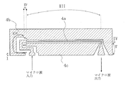
図1に本発明の実施形態に使用する中心導体4a、接地導体4b、4cからなるCPW進行波電極4の上面図を示す。この第1の実施形態においても第1の従来技術や第2の従来技術と同様に、Iは入力用フィードスルー部であり、不図示のコネクタの芯線に接続される。またこの不図示のコネクタの芯線は外部回路である不図示のドライバに接続される。IIIは相互作用部、IVは出力側接続部、及びVは出力用フィードスルー部である。出力用フィードスルー部Vが不図示のコネクタの芯線(あるいは金リボンや金ワイヤー)もしくは終端抵抗に接続されるのも同じである。VIIはインピーダンス変換部である。ここで、図2に図1の等価回路を示す。なお、図2には示していないが、図1の相互作用部IIIの特性インピーダンスをZ3とする。図2においてZin’’は外部信号源5と外部信号源5の負荷抵抗6から本実施形態のx−カット基板LN光変調器を見た入力インピーダンスである。
[First Embodiment]
FIG. 1 shows a top view of a CPW
本実施形態においても駆動電圧を低減するために、相互作用部IIIの特性インピーダンスZ3(あるいは、第2の従来技術と同様に合成部III’の特性インピーダンスZ3’)を30Ω程度に低減している。そして、本発明の目的はこの低駆動電圧性と、電気的反射特性の改善、即ち外部信号源へ戻る電気的反射波を抑圧することによる光パルスのジッタの改善に重きを置いている。 Also in this embodiment, in order to reduce the driving voltage, the characteristic impedance Z 3 of the interaction part III (or the characteristic impedance Z 3 ′ of the synthesis part III ′ as in the second conventional technique) is reduced to about 30Ω. ing. The object of the present invention is focused on the low driving voltage and the improvement of the electric reflection characteristics, that is, the improvement of the jitter of the optical pulse by suppressing the electric reflection wave returning to the external signal source.
この本発明の第1の実施形態は第2の従来技術と同様に線路16からなり、特性インピーダンスZ7を有するインピーダンス変換部VIIを有している。ここで、注意すべきことは、第2の従来技術ではインピーダンス変換部VIの特性インピーダンスZ6は入力用フィードスルー部Iの特性インピーダンスZ1と、相互作用部IIIの特性インピーダンスZ3との相乗平均であり、またインピーダンス変換部VIの長さL6は高周波電気信号のビットレートに対する管内波長をλとしてλ/4と設定しているが、この本実施形態ではそうなっていない。
The first embodiment of the present invention consists of the second prior art as well as the
つまり、インピーダンス変換領域VIIの特性インピーダンスZ7は入力用フィードスルー部Iの特性インピーダンスZ1と相互作用部IIIの特性インピーダンスZ3との相乗平均でもないし、入力用フィードスルー部Iの特性インピーダンスZ1と、相互作用部IIIと出力用フィードスルー部Vなどとの合成部III’の特性インピーダンスZ3’との相乗平均でもない。またインピーダンス変換部VIIの長さL7が高周波電気信号のビットレートの管内波長をλとしてλ/4である必要はない。 That is, neither in the geometric mean of the characteristic impedance Z 1 and the interaction portion characteristic impedance Z 3 of III characteristic impedance Z 7 is input feed-through portion I of the impedance conversion area VII, the characteristic impedance Z of the input feed-through portion I 1 and the geometrical mean of the characteristic impedance Z 3 ′ of the combined portion III ′ of the interaction portion III and the output feedthrough portion V or the like. The impedance length L 7 of the conversion unit VII need not be lambda / 4 the guide wavelength as lambda bit rate of a high-frequency electrical signals.
これらのことは、入力用フィードスルー部Iとインピーダンス変換部VIIをまとめてインピーダンス変換部と考えた場合も同じである。その場合の等価回路を図3に示す。ここで、VII’は入力用フィードスルー部Iとインピーダンス変換部VIIの合成部である。ここで、合成部VII’の特性インピーダンスをZ8とすると、特性インピーダンスZ8は、コネクタの特性インピーダンス(あるいは外部信号源5の特性インピーダンスRg)と相互作用部IIIの特性インピーダンスZ3との相乗平均でもないし、コネクタの特性インピーダンス(あるいは外部信号源5の特性インピーダンスRg)と合成部III’の特性インピーダンスZ3’との相乗平均でもない。勿論、この場合でもインピーダンス変換部VIIの長さL7はおろか、入力用フィードスルー部Iの長さとインピーダンス変換部VIIの長さL7の和が高周波電気信号のビットレートの周波数(例えば、高周波電気信号のビットレートが10Gbit/sの場合には10GHz)における管内波長をλとしてλ/4である必要はない。 The same applies to the case where the input feedthrough part I and the impedance conversion part VII are collectively considered as the impedance conversion part. An equivalent circuit in that case is shown in FIG. Here, VII ′ is a composite part of the input feedthrough part I and the impedance conversion part VII. Here, assuming that the characteristic impedance of the synthesis unit VII ′ is Z 8 , the characteristic impedance Z 8 is a synergy between the characteristic impedance of the connector (or the characteristic impedance Rg of the external signal source 5) and the characteristic impedance Z 3 of the interaction unit III. It is neither an average nor a geometrical average of the characteristic impedance of the connector (or the characteristic impedance Rg of the external signal source 5) and the characteristic impedance Z 3 ′ of the synthesis unit III ′. Of course, the length L 7, let alone impedance converter VII In this case, input the sum of the length L 7 of the length and impedance transformation portion VII of the feed-through portion I is the bit rate of the high-frequency electrical signal frequency (e.g., radio frequency When the bit rate of the electrical signal is 10 Gbit / s, the wavelength in the tube at 10 GHz is not required to be λ / 4.
ここで、さらに詳しく考察する。まず、上において述べたように本発明ではインピーダンス変換部VIIの特性インピーダンスZ7は、第2の従来技術と異なり、入力用フィードスルー部Iの特性インピーダンスZ1と相互作用部IIIの特性インピーダンスZ3との相乗平均でもないし、また入力用フィードスルー部Iの特性インピーダンスZ1と、相互作用部IIIと出力用フィードスルー部Vなどとの合成部III’の特性インピーダンスZ3’との相乗平均でもない。 Now consider in more detail. First, as described above, in the present invention, the characteristic impedance Z 7 of the impedance conversion unit VII differs from the second conventional technique in that the characteristic impedance Z 1 of the input feed-through unit I and the characteristic impedance Z of the interaction unit III are different. 3, and the geometrical average of the characteristic impedance Z 1 of the input feedthrough part I and the characteristic impedance Z 3 ′ of the combined part III ′ of the interaction part III and the output feedthrough part V etc. not.
それどころか、上において述べたように、本発明では入力用フィードスルー部Iもインピーダンス変換部の一部として機能させることもできるので、入力用フィードスルー部Iの特性インピーダンスZ1をインピーダンス変換部VIIの特性インピーダンスZ7に等しくしておいても良い。 Rather, as mentioned in the above, since the present invention can also function as part of the input feed-through portion I the impedance conversion portion, the characteristic impedance Z 1 of the input feed-through portion I of the impedance conversion section VII it may have been equal to the characteristic impedance Z 7.
というのは、実際には入力用フィードスルー部Iには不図示のコネクタの芯線(以下、省略するが、金リボンや金ワイヤーなどが接続されることもある)が接続されており、この不図示のコネクタの芯線はその直径が100〜300μmと大きな(あるいは厚い)導体であるので、これを接続することにより入力用フィードスルー部Iの特性インピーダンスを大きく低下させる効果がある。 This is because a connector core wire (not shown) (which may be connected to a gold ribbon or a gold wire in some cases) is connected to the input feed-through section I in practice. Since the core wire of the illustrated connector is a large (or thick) conductor having a diameter of 100 to 300 μm, connecting this has the effect of greatly reducing the characteristic impedance of the input feedthrough I.
従って、入力用フィードスルー部Iの実効的な特性インピーダンスZ1(正確には、コネクタの芯線の導体によるインピーダンス低下の影響を受けた入力用フィードスルー部Iの実効的な特性インピーダンスであり、コネクタの芯線を考慮しない場合のZ1よりも低いのでZ1と区別するためにZ1’とすべきではあるが、ここでは簡単のためにZ1と記載する)はインピーダンス変換部VIIの特性インピーダンスZ7よりも低くなる。 Therefore, the effective characteristic impedance Z 1 of the input feedthrough portion I (more precisely, the effective characteristic impedance of the input feedthrough portion I affected by the impedance drop due to the conductor of the connector core wire, Is lower than Z 1 when the core wire is not taken into account, it should be Z 1 ′ to distinguish from Z 1 , but here it is referred to as Z 1 for simplicity) is the characteristic impedance of the impedance converter VII It is lower than the Z 7.
その結果、例え、インピーダンス変換部VIIの特性インピーダンスZ7と入力用フィードスルー部Iの特性インピーダンスZ1を、不図示のコネクタの特性インピーダンス(あるいは外部信号源の特性インピーダンスRg)と相互作用部IIIの特性インピーダンスZ3との相乗平均、もしくは不図示のコネクタの特性インピーダンス(あるいは外部信号源の特性インピーダンスRg)と、相互作用部IIIと出力用フィードスルー部Vなどとの合成部III’の特性インピーダンスZ3’との相乗平均としても、不図示のコネクタの芯線などを接続した入力用フィードスルー部Iの特性インピーダンスZ1(以下、省略するが、前述のように接続したコネクタの芯線のために、低くなった実効的な特性インピーダンスを指す)はこれらの相乗平均の値よりもかなり低くなっている。 As a result, for example, the characteristic impedance Z 7 of the impedance conversion unit VII and the characteristic impedance Z 1 of the input feedthrough unit I are changed to the characteristic impedance of the connector (not shown) (or the characteristic impedance Rg of the external signal source) and the interaction unit III. characteristics of geometric mean between the characteristic impedance Z 3 of, or not shown connector characteristic impedance (or an external signal source characteristic impedance Rg) and the synthesis section III and the like output feed-through portion V and the interaction portion III ' As a geometric average with the impedance Z 3 ′, the characteristic impedance Z 1 of the input feedthrough I to which a connector core wire (not shown) is connected (hereinafter omitted, because of the connector core wire connected as described above) Is the effective characteristic impedance that has been lowered) It is considerably lower than the value of the geometric mean.
そのため、インピーダンス変換の機能を有する部位全体(つまり、入力用フィードスルー部Iとインピーダンス変換部VIIの合成部VII’)について考えると、合成部VII’の特性インピーダンスZ8は上記の相乗平均の値にはなっておらず、より低い値となっている。換言すると、入力用フィードスルー部Iは、インピーダンス変換の機能を有する部位全体VII’(あるいは合成部VII’)の特性インピーダンスZ8を前述の相乗平均からずらす効果を持ち、残留反射を生じつつ広い周波数帯域におけるインピーダンス変換を実現するインピーダンス変換を実現する。 Therefore, the entire portion having a function of impedance conversion (i.e., the combining unit VII of the input feed-through portion I and the impedance converting section VII ') Considering, combining unit VII' characteristic impedance Z 8 above the geometric mean of the values of It is not, and it is a lower value. Wide In other words, the input feed-through portion I is the characteristic impedance Z 8 sites across VII '(or synthetic unit VII') having a function of impedance transformation has the effect of shifting the geometric mean of the above, while resulting residual reflection Impedance conversion for realizing impedance conversion in the frequency band is realized.
つまり、コネクタの芯線を接続することにより、故意に入力用フィードスルーの特性インピーダンスを小さくし、インピーダンス変換の機能を有する部位全体VII’(入力用フィードスルー部Iとインピーダンス変換部VIIの合成部VII’)の特性インピーダンスが上述の相乗平均にならないようにすることにより、残留反射を生じさせ、結果的にインピーダンス変換の機能を実現できる周波数を広帯域化している。 That is, by connecting the connector core wire, the characteristic impedance of the input feedthrough is intentionally reduced, and the entire portion VII ′ having the function of impedance conversion (the combined portion VII of the input feedthrough portion I and the impedance conversion portion VII) By preventing the characteristic impedance of ') from becoming the above-mentioned geometric average, residual reflection is caused, and as a result, the frequency at which the impedance conversion function can be realized is widened.
さらには、入力用フィードスルー部Iの特性インピーダンスZ1をコネクタ(あるいは、外部信号源の特性インピーダンスRg)と同じほぼ50Ωとし、インピーダンス変換部VIIの特性インピーダンスZ7を、入力用フィードスルー部Iの特性インピーダンスZ1と相互作用部IIIの特性インピーダンスZ3(もしくは相互作用部IIIと出力用フィードスルー部Vなどとの合成部III’の特性インピーダンスZ3’)との相乗平均とした場合について考える。 Furthermore, the connector characteristic impedance Z 1 of the input feed-through portion I (or characteristic impedance Rg of the external signal source) and the same substantially 50 [Omega, the characteristic impedance Z 7 of the impedance conversion section VII, input feed-through portion I the case of the characteristic impedance Z 1 and the interaction portion III of the characteristic impedance Z 3 (or 'characteristic impedance Z 3 of' synthesis section III of the interaction portion III and the like output feed-through section V) geometric mean and the Think.
これまで説明したように、不図示のコネクタの芯線を接続した入力用フィードスルー部Iの特性インピーダンスZ1は実際には著しく低下する。従って、インピーダンス変換部VIIの特性インピーダンスZ7は、相互作用部IIIの特性インピーダンスZ3(もしくは相互作用部IIIと出力用フィードスルー部Vなどとの合成部III’の特性インピーダンスZ3’)と、接続されたコネクタの芯線のために実際にはかなり低くなった入力用フィードスルー部Iの特性インピーダンスZ1との相乗平均と等しくはならず、この相乗平均より高くなる。 As has been described, the characteristic impedance Z 1 of the input feed-through portion I of connecting the connector core of the not shown drops actually significantly. Therefore, the characteristic impedance Z 7 of the impedance conversion unit VII is equal to the characteristic impedance Z 3 of the interaction unit III (or the characteristic impedance Z 3 ′ of the synthesis unit III ′ of the interaction unit III and the output feedthrough unit V). actually geometric mean equally does not become the characteristic impedance Z 1 of the input feed-through portion I which is much lower for the core wire of connector connected becomes higher than the geometric mean.
このようにして、最終的にインピーダンス変換部VIIの特性インピーダンスZ7を、コネクタの芯線を接続した入力用フィードスルー部Iの特性インピーダンスZ1と相互作用部IIIの特性インピーダンスZ3(もしくは相互作用部IIIと出力用フィードスルー部Vなどとの合成部III’の特性インピーダンスZ3’)との相乗平均からずらした結果、残留反射が生じ、結果的にインピーダンス変換機能の周波数を広帯域化することができる。つまり、入力用フィードスルー部Iはインピーダンス変換の周波数を広帯域化するためのインピーダンス変換部の一部として動作することになる。 In this way, finally the characteristic impedance Z 7 of the impedance conversion section VII, the characteristic impedance of the input feed-through portion I of connecting the core wire of the connector Z 1 interacting portion III of the characteristic impedance Z 3 (or interactions As a result of shifting from the geometric mean of the characteristic impedance Z 3 ′) of the combined part III ′ of the part III and the output feed-through part V and the like, residual reflection occurs, and consequently the frequency of the impedance conversion function is widened. Can do. That is, the input feedthrough section I operates as a part of an impedance conversion section for widening the frequency of impedance conversion.
本発明では入力用フィードスルー部Iとインピーダンス変換部VIIとを区別して呼んではいるが、これまで説明したように入力用フィードスルー部Iもインピーダンス変換機能を有しており、入力用フィードスルー部Iとインピーダンス変換部VIIの部位全体として、インピーダンス変換部を構成している。そして、この部位全体として前述の相乗平均が成り立たないように設定している。 In the present invention, the input feedthrough part I and the impedance conversion part VII are distinguished and called. However, as described above, the input feedthrough part I also has an impedance conversion function, and the input feedthrough part I As a whole part of I and the impedance conversion unit VII, an impedance conversion unit is configured. And it sets so that the above-mentioned geometrical average may not be materialized as this whole site | part.
つまり、コネクタの芯線を接続していない状態での入力用フィードスルー部Iの特性インピーダンスZ1がインピーダンス変換部VIIの特性インピーダンスZ7に等しい場合でも、あるいは等しくない場合でも、インピーダンス変換部VIIの特性インピーダンスZ7を最初から上記の相乗平均からずらしても良いし、コネクタの芯線を接続することにより入力用フィードスルー部Iの特性インピーダンスZ1を低くした結果、インピーダンス変換部VIIの特性インピーダンスZ7が上記の相乗平均からずれても良い。さらに、コネクタの芯線を接続することにより、入力用フィードスルー部Iとインピーダンス変換部VIIの全体からなるインピーダンス変換機能を有する部位全体の特性インピーダンスを上記の相乗平均からずらしても良いことは言うまでもない。本発明ではこのようにして、インピーダンス変換の機能を有する部位の特性インピーダンスを上記の相乗平均からずらすことにより、残留反射を生じつつ、インピーダンス変換機能の周波数の広帯域化を図っている。そして、これらの考え方は本発明の全ての実施形態に当てはまる。 That is, even when the characteristic impedance Z 1 of the input feed-through portion I, which does not connect the core wire of the connector is equal to the characteristic impedance Z 7 of the impedance conversion section VII, or even if not equal, impedance converter VII The characteristic impedance Z 7 may be shifted from the above geometric mean from the beginning, and the characteristic impedance Z 1 of the input feedthrough part I is lowered by connecting the core wire of the connector. 7 may deviate from the geometric mean described above. Furthermore, it goes without saying that the characteristic impedance of the entire part having the impedance conversion function consisting of the input feedthrough part I and the impedance conversion part VII may be shifted from the above geometric mean by connecting the core wires of the connector. . In the present invention, the characteristic impedance of the portion having the function of impedance conversion is shifted from the geometric average as described above, so that the frequency of the impedance conversion function is widened while causing residual reflection. These ideas apply to all embodiments of the present invention.
また、本発明においてはインピーダンス変換部VIIの長さL7は高周波電気信号のビットレートにおける管内波長(例えば、高周波電気信号のビットレートが10Gbit/sであれば10GHzにおける管内波長)をλとして第2の従来技術のようにλ/4とする必要はない。つまり、本発明では入力用フィードスルー部Iもインピーダンス変換部の一部であるから、あえてインピーダンス変換部の長さをあげるとするとインピーダンス変換部VIIと入力用フィードスルー部Iの電気的な長さの和となる。 In the present invention, the length L 7 of the impedance conversion unit VII is set such that the in-tube wavelength at the bit rate of the high-frequency electric signal (for example, the in-tube wavelength at 10 GHz if the bit rate of the high-frequency electric signal is 10 Gbit / s) is λ. It is not necessary to set λ / 4 as in the prior art of No. 2. That is, in the present invention, since the input feedthrough part I is also a part of the impedance conversion part, the electrical length of the impedance conversion part VII and the input feedthrough part I is assumed to increase the length of the impedance conversion part. The sum of
但し、そもそも前述の相乗平均の考え方を用いていないので、インピーダンス変換部VIIと入力用フィードスルー部Iの電気的な長さの和を高周波電気信号のビットレートの管内波長をλとしてλ/4とする必要もない。なお、この電気的な長さの和はこのλ/4よりも長い方が好ましいようである。 However, since the above-described geometric average concept is not used in the first place, the sum of the electrical lengths of the impedance conversion unit VII and the input feedthrough unit I is λ / 4 where the in-tube wavelength of the bit rate of the high-frequency electrical signal is λ. There is no need to do. It seems that the sum of the electrical lengths is preferably longer than λ / 4.
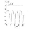
さて、本実施形態においては駆動電圧を低減するために、相互作用部IIIの特性インピーダンスZ3(あるいは、出力用フィードスルー部Vは相互作用部IIIとほぼ同じ特性インピーダンスを有するとし、出力用フィードスルー部Vと相互作用部IIIとの合成部III’の特性インピーダンスZ3’は相互作用部IIIの特性インピーダンスZ3と同じとする)を30Ω程度に低減している。この場合のパワー反射率S11(厳密にはパワー反射率S11の包絡線)を図4に示す。図からわかるように、11.3Gbit/sのビットレートの20%から30%の周波数帯内の3GHz付近において−12dB程度の残留反射を持つパワー反射率S11の特性となっている。このように、本発明の光変調器では、ビットレートの20%から30%にあたる周波数帯内の少なくとも1点において、パワー反射率S11は−10dBから−15dBの間にある。そして、ビットレートの周波数の40%から70%にあたる周波数帯域内にパワー反射率が−15dB以下の極小値がある。 In the present embodiment, in order to reduce the drive voltage, it is assumed that the characteristic impedance Z 3 of the interaction unit III (or the output feedthrough unit V has substantially the same characteristic impedance as that of the interaction unit III). The characteristic impedance Z 3 ′ of the combined part III ′ of the feedthrough part V and the interaction part III is assumed to be the same as the characteristic impedance Z 3 of the interaction part III). The power reflectivity S 11 in this case (strictly speaking, the envelope of the power reflectivity S 11 ) is shown in FIG. As can be seen from the figure, the power reflectivity S 11 has a residual reflection of about −12 dB in the vicinity of 3 GHz in the frequency band of 20% to 30% of the bit rate of 11.3 Gbit / s. Thus, in the optical modulator of the present invention, at least one point within the frequency band from 20% corresponding to 30% of the bit rate, the power reflectivity S 11 is between -10dB of -15 dB. Then, there is a minimum value with a power reflectance of −15 dB or less in a frequency band corresponding to 40% to 70% of the frequency of the bit rate.
なお、出力用フィードスルー部Vと相互作用部IIIとをほぼ同じ特性インピーダンスとするために、図1からわかるように出力用フィードスルー部Vにおける中心導体を非線形テーパ形状とし、また中心導体と接地導体の間に設けたギャップの形状も非線形とした。そして、このような出力用フィードスルー部Vの非線形形状は本発明の全ての実施形態について適用可能である。但し、非線形形状が好適であるという意味であり、本発明の効果を発揮できる最重要事項というわけではない。 In order to make the output feedthrough portion V and the interaction portion III have substantially the same characteristic impedance, the center conductor in the output feedthrough portion V has a non-linear taper shape as shown in FIG. The shape of the gap provided between the conductors was also non-linear. Such a nonlinear shape of the output feed-through portion V can be applied to all the embodiments of the present invention. However, this means that a non-linear shape is suitable, and it is not the most important matter that can exhibit the effects of the present invention.
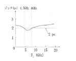
本実施形態では、(2)式や(3)式が成り立っていないので、図26に示した第2の従来技術のような特定の周波数において電気的なパワー反射率S11が極めて良くなることはない。しかしながら、11.3Gbit/sの伝送速度について図4に示すように、11.3Gbit/sのパルスの基本周波数である5.6GHzの領域において電気的パワー反射率S11が−15dB以下であり、かつある程度の幅の周波数帯域において充分なパワー反射率特性S11となっている(なお、厳密には、図4のS11はパワー反射率の包絡線であり、ここではそれをパワー反射率と呼んでいる)。この時、パワー反射率S11の包絡線が谷となる(つまり、パワー反射率S11の包絡線の一次微分がゼロで、二次微分が正となる極小値を与える)周波数Fcが重要となる。 In this embodiment, (2) since the type or (3) does not consist, the electrical power reflectance S 11 is very well in the second specific frequency, such as the prior art shown in FIG. 26 There is no. However, as shown in FIG. 4 for the transmission speed of 11.3 Gbit / s, the electrical power reflectance S 11 is −15 dB or less in the region of 5.6 GHz which is the fundamental frequency of the pulse of 11.3 Gbit / s, In addition, a sufficient power reflectivity characteristic S 11 is obtained in a frequency band of a certain width (strictly speaking, S 11 in FIG. 4 is an envelope of the power reflectivity, and here it is referred to as a power reflectivity. Calling). In this case, the envelope of the power reflectance S 11 becomes a valley (i.e., first derivative of the envelope of the power reflectance S 11 is zero, giving the minimum value second derivative is positive) frequency Fc is important Become.
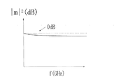
図5には11.3Gbit/sの伝送速度の場合について、図4におけるパワー反射率S11の極小点(あるいはパワー反射率S11の包絡線の谷)Fcを変数にした場合の光パルスが有するジッタを示している。図からわかるように、パワー反射率S11の極小点Fcが伝送速度(11.3Gbit/s)の40%から70%の間の周波数帯にあり、そのパワー反射率S11の絶対値が−15dB以下であれば、ジッタは伝送時のエラーがほとんど増加しない2ps以下の値となっている。また、図6には光変調指数の周波数依存性を示している。図からわかるように、本発明を適用することにより、光変調帯域も改善できた。 FIG. 5 shows an optical pulse when the minimum point of the power reflectivity S 11 in FIG. 4 (or the valley of the envelope of the power reflectivity S 11 ) Fc is used as a variable for a transmission speed of 11.3 Gbit / s. It shows jitter having. As can be seen, minimum point Fc of the power reflectance S 11 is in the frequency band between 70% to 40% of the transmission rate (11.3 Gbit / s), the absolute value of the power reflectance S 11 - If it is 15 dB or less, the jitter has a value of 2 ps or less, which hardly increases errors during transmission. FIG. 6 shows the frequency dependence of the light modulation index. As can be seen from the figure, by applying the present invention, the light modulation band can also be improved.
このように、駆動電圧を低く保ったまま(この結果、約2GHzから約3GHzの周波数の領域において、パワー反射率S11が−10dBから−15dBの間と悪くなってしまうが、NRZ型の変調形式の場合にはこの領域における周波数スペクトルは小さい)、光パルスのジッタを低減できる、あるいは光変調帯域を広くできるなど、光変調器としての高性能化を図ることが可能となる。なお、このビットレートの20%から30%、あるいはビットレートの40%から70%という値は10Gbit/sや11.3Gbit/s以外のその他の各種ビットレート、例えば12.5Gbit/s、25Gbit/s、43Gbit/s、50Gbit/s、100Gbit/sでも成り立つ。 In this way, the drive voltage is kept low (as a result, the power reflectivity S 11 becomes worse between −10 dB and −15 dB in the frequency range of about 2 GHz to about 3 GHz. In the case of the format, the frequency spectrum in this region is small), the jitter of the optical pulse can be reduced, or the optical modulation band can be widened, so that high performance as an optical modulator can be achieved. The values of 20% to 30% of the bit rate, or 40% to 70% of the bit rate are other bit rates other than 10 Gbit / s and 11.3 Gbit / s, for example, 12.5 Gbit / s, 25 Gbit / s. Even s, 43 Gbit / s, 50 Gbit / s, and 100 Gbit / s are established.
なお、20%から30%という値は、ビットレートが10Gbit/sから12.5Gbit/sの場合は約2GHzから3.7GHzに、ビットレートが25Gbit/sの場合は約5GHzから8GHzに、ビットレートが43Gbit/sの場合は約9GHzから13GHzに、ビットレートが54Gbit/sの場合は約11GHzから16GHzに、ビットレートが110Gbit/sの場合は約22GHzから33GHzに対応する。 The value of 20% to 30% is a bit rate from about 2 GHz to 3.7 GHz when the bit rate is 10 Gbit / s to 12.5 Gbit / s, and from about 5 GHz to 8 GHz when the bit rate is 25 Gbit / s. When the rate is 43 Gbit / s, it corresponds from about 9 GHz to 13 GHz, when the bit rate is 54 Gbit / s, it corresponds from about 11 GHz to 16 GHz, and when the bit rate is 110 Gbit / s, it corresponds from about 22 GHz to 33 GHz.
そして、40%から70%という値は、ビットレートが10Gbit/sから12.5Gbit/sの場合は約4GHzから9GHzに、ビットレートが25Gbit/sの場合は約10GHzから18GHzに、ビットレートが43Gbit/sの場合は約17GHzから30GHzに、ビットレートが54Gbit/sの場合は約22GHzから38GHzに、ビットレートが110Gbit/sの場合は約44GHzから77GHzに対応する。 The value of 40% to 70% is about 4 GHz to 9 GHz when the bit rate is 10 Gbit / s to 12.5 Gbit / s, and about 10 GHz to 18 GHz when the bit rate is 25 Gbit / s. In the case of 43 Gbit / s, it corresponds from about 17 GHz to 30 GHz, in the case of a bit rate of 54 Gbit / s, from about 22 GHz to 38 GHz, and in the case of a bit rate of 110 Gbit / s, it corresponds from about 44 GHz to 77 GHz.
なお、本発明ではパワー反射率S11の極小点Fcが伝送速度(例えば10Gbit/sや11.3Gbit/sなど)の40%から70%の間に存在することが重要であるが、これは第1の従来技術はおろか第2の従来技術の考え方でも実現できない。 Note that in the present invention it is important that the minimum point Fc of the power reflectance S 11 is present between 70% to 40% of the transmission rate (for example, 10Gbit / s and 11.3 Gbit / s, etc.), which The first prior art as well as the second prior art cannot be realized.
つまり、これを実現するには、コネクタの芯線を接続することによる入力フィードスルー部Iの特性インピーダンスZ1の低下を考慮することが好適である。インピーダンス変換部VIIの特性インピーダンスZ7のみならず、入力用フィードスルー部Iもインピーダンス変換部と考えて、入力用フィードスルー部Iとインピーダンス変換部VIIとの合成部VII’の特性インピーダンスZ8を、外部信号源5の特性インピーダンスRg(あるいは、負荷抵抗、出力インピーダンス、インピーダンスと呼ばれ、一般に、不図示のコネクタの特性インピーダンスと等しいことが望ましい)と、相互作用部IIIの特性インピーダンスZ3や、不図示の相互作用部IIIと不図示の出力フィードスルー部などとの合成部III’の特性インピーダンスZ3’との相乗平均と異ならしめることが効果的である。 That is, to realize this, it is preferable to consider the reduction of the characteristic impedance Z 1 of the input feed-through portion I by connecting the core wire of the connector. Considering not only the characteristic impedance Z 7 of the impedance conversion unit VII but also the input feed-through unit I as an impedance conversion unit, the characteristic impedance Z 8 of the synthesis unit VII ′ of the input feed-through unit I and the impedance conversion unit VII is The characteristic impedance Rg of the external signal source 5 (or called the load resistance, the output impedance, and the impedance, and generally desirable to be equal to the characteristic impedance of the connector not shown), the characteristic impedance Z 3 of the interaction unit III, It is effective to make it different from the geometric mean of the characteristic impedance Z 3 ′ of the synthesis part III ′ of the interaction part III (not shown) and the output feedthrough part (not shown).
また、本発明ではインピーダンス変換部VII(ここで、入力用フィードスルー部Iもインピーダンス変換部としても良い)は一段構成としたが、本発明ではパワー反射率S11の極小点Fcが伝送速度(例えば10Gbit/sや11.3Gbit/sなど)の40%から70%の間に存在し、その極小値FCにおけるパワー反射率S11が−15dB以下となるように設定することが重要であり、これにより変調帯域を改善するとともに特に光パルスのジッタを低減することが特徴であるので、一段構成でなくても2段、あるいは3段以上の多段構成でも良いことは言うまでもない。 Further, (wherein also good as the input feed-through portion I also impedance converter) impedance transformation portion VII in the present invention has been is a single-stage configuration, minimum point Fc is the transmission speed of the power reflectance S 11 in the present invention ( for example exists between 40% such as 10Gbit / s and 11.3 Gbit / s) of 70%, the power reflectivity S 11 at the minimum value F C is important to set to be equal to or less than -15dB Thus, since the modulation band is improved and the jitter of the optical pulse is particularly reduced, it is needless to say that the multi-stage configuration including two stages or three or more stages may be used instead of the one-stage configuration.
なお、コネクタの特性インピーダンスは一般に50Ωであり、相互作用部IIIの特性インピーダンスZ3や合成部III’の特性インピーダンスZ3’は30Ωであるので、これらの相乗平均は38.7Ωとなる。残留反射を生じつつ、インピーダンス変換機能を発揮できる周波数を広帯域化するという本発明の効果を発揮するためには、インピーダンス変換部VIIの特性インピーダンスZ7の値をこの相乗平均の値と異ならしめると効果的である。そこで、入力用フィードスルー部Iとインピーダンス変換部VIIは44Ω(なお、33Ωなどでも良い)とした。 The characteristic impedance of the connector is generally 50 [Omega, since 'the characteristic impedance Z 3 of' the characteristic impedance of the interaction portion III Z 3 and combining unit III is a 30 [Omega, these geometric mean becomes 38.7Omu. While resulting residual reflection, the frequency capable of exhibiting an impedance conversion function in order to exhibit the effect of the present invention that broadband, when made different values of characteristic impedance Z 7 impedance converter VII to the value of the geometric mean It is effective. Therefore, the input feedthrough section I and the impedance conversion section VII are 44Ω (33Ω or the like may be used).
但し、入力用フィードスルー部Iには不図示のコネクタの芯線が固定されており、この不図示のコネクタの芯線は直径が100〜300μm程度の大きな(あるいは厚い)導体で構成されている。そのため、不図示のコネクタの芯線を考慮した入力用フィードスルー部Iの特性インピーダンスは29Ω(なお、インピーダンス変換部VIIが33Ωの時は、不図示のコネクタの芯線を考慮した入力用フィードスルー部Iの特性インピーダンスは25Ωに設定した)とますます前述の相乗平均の値と大きく異なっている。 However, a core wire of a connector (not shown) is fixed to the input feed-through portion I, and the core wire of the connector (not shown) is made of a large (or thick) conductor having a diameter of about 100 to 300 μm. Therefore, the characteristic impedance of the input feed-through portion I considering the core wire of the connector (not shown) is 29Ω (when the impedance conversion portion VII is 33Ω, the input feed-through portion I considering the core wire of the connector not shown) The characteristic impedance is set to 25 Ω) and is much different from the above-mentioned geometric mean value.
ここで、入力用フィードスルー部Iの特性インピーダンスZ1とインピーダンス変換部VIIの特性インピーダンスZ7とを前述の相乗平均である38.7Ωとした場合について考察する。入力用フィードスルー部Iには不図示のコネクタの芯線が接続されているために、その実効的な特性インピーダンスZ1はインピーダンス変換部VIIの特性インピーダンスZ7(38.7Ω)よりも実際には大幅に(10Ω前後も)低くなる。その結果、入力用フィードスルー部Iの特性インピーダンスZ1(正確には、入力用フィードスルー部Iのコネクタの芯線のために低くなった実効的な特性インピーダンスZ1とも言える)とインピーダンス変換部VIIからなるインピーダンス変換の部位全体VII’としての特性インピーダンスZ8は先の相乗平均(38.7Ω)よりも低い値となる。そして、さらにはこの低くなった実効的な特性インピーダンスZ1は相互作用部IIIの特性インピーダンスZ3(あるいは、合成部の特性インピーダンスZ3’で、ここでは約30Ω)よりも低い場合がある。 Here, consider the case where the characteristic impedance Z 7 of the characteristic impedance Z 1 and the impedance converting section VII of the input feed-through portion I to be the geometric mean of the above 38.7Omu. The input feed-through portion I for being connected to the core wire of the connector (not shown), the effective characteristic impedance Z 1 actually than the characteristic impedance Z 7 of the impedance conversion section VII (38.7Ω) is Significantly lower (around 10Ω). As a result, the characteristic impedance Z 1 of the input feedthrough part I (to be precise, it can be said that the effective characteristic impedance Z 1 is lowered due to the core wire of the connector of the input feedthrough part I) and the impedance conversion part VII. The characteristic impedance Z 8 as the whole region VII ′ of the impedance conversion consisting of is a value lower than the geometric mean (38.7Ω). Further, the lowered effective characteristic impedance Z 1 may be lower than the characteristic impedance Z 3 of the interaction part III (or the characteristic impedance Z 3 ′ of the synthesis part, here about 30Ω).
このように、入力用フィードスルー部Iとインピーダンス変換部VIIからなるインピーダンス変換の部位全体VII’としての特性インピーダンスZ8を前述の相乗平均からずらすことにより、残留反射を生じつつ、インピーダンス変換機能を発揮できる周波数を広帯域化するという本発明の効果を発揮することが可能となる。
なお、光パルスのジッタを2ps以下とするには、インピーダンス変換部VIIの特性インピーダンスZ7や入力用フィードスルー部Iの特性インピーダンスZ1を前述の相乗平均から2Ω(好適には3Ω)以上離した方が良い。また、入力用フィードスルー部Iの特性インピーダンスZ1についてはコネクタの芯線を接続することにより、結果的にその値を小さくすることが有効である。そしてこれらのことは本発明の全ての実施形態について言える。
Thus, by shifting the characteristic impedance Z 8 as a whole part of the impedance conversion consisting of an input feed-through portion I and the impedance converting section VII VII 'from the geometric mean of the above, while resulting residual reflection, an impedance conversion function The effect of the present invention of widening the frequency that can be exhibited can be exhibited.
In order to set the jitter of the optical pulse to 2 ps or less, the characteristic impedance Z 7 of the impedance conversion unit VII and the characteristic impedance Z 1 of the input feedthrough unit I are separated from the above geometric average by 2Ω (preferably 3Ω) or more. Better to do. Further, the characteristic impedance Z 1 of the input feed-through portion I is by connecting the core of the connector, it is effective to reduce the result to the value. These are true for all embodiments of the invention.
そして、不図示のコネクタと相互作用部IIIの間に部分的に相互作用部IIIの特性インピーダンス(あるいは、相互作用部IIIを含む合成部の特性インピーダンスZ3’)の値よりも低い部分があっても良いし、逆に好都合であると言える。なぜなら、本発明における重要な点はパワー反射率S11の包絡線の極小点Fcがビットレート(例えば10Gbit/sや11.3Gbit/s、25Gbit/s、50Gbit/s、100Gbit/sなど)の周波数(例えば10GHzや11.3GHz、25GHz、50GHz、100GHzなど)の40%から70%の間に存在し、かつその極小点Fcにおけるパワー反射率S11が−15dB以下となるように、設定することであり、この考え方は第2の従来技術には開示されておらず、また第2の従来技術の考え方では決して実現できない。つまり、(2)式や(3)式が成り立たない条件でしか実現できないからである。 Further, there is a portion between the connector (not shown) and the interaction part III that is partly lower than the characteristic impedance of the interaction part III (or the characteristic impedance Z 3 ′ of the combined part including the interaction part III). However, it can be said that it is convenient. The important point in the present invention is that the minimum point Fc of the envelope of the power reflectivity S 11 is the bit rate (for example, 10 Gbit / s, 11.3 Gbit / s, 25 Gbit / s, 50 Gbit / s, 100 Gbit / s, etc.). frequency (e.g. 10GHz and 11.3GHz, 25GHz, 50GHz, 100GHz, etc.) exist between 40% to 70% and so that the power reflectivity S 11 at the minimum point Fc is equal to or less than -15 dB, set Therefore, this concept is not disclosed in the second prior art, and cannot be realized by the second prior art. In other words, this is because it can be realized only under a condition where Expressions (2) and (3) do not hold.
さらに、本発明ではインピーダンス変換部の特性インピーダンスに前述の相乗平均の値を用いないので、残留反射を完全に抑圧しようとする第2の従来技術の考え方と全く異なり、意図的に広い周波数領域において残留反射を生じさせつつ、かつ必要なレベルにまでその残留反射の値を抑圧するとも言える。 Furthermore, in the present invention, since the above-mentioned geometric mean value is not used for the characteristic impedance of the impedance converter, it is completely different from the concept of the second prior art in which residual reflection is completely suppressed, and intentionally in a wide frequency range. It can be said that the residual reflection value is suppressed to a necessary level while causing the residual reflection.
[第2の実施形態]
図7に本発明の第2の実施形態に使用するCPW進行波電極4の上面図を示す。本実施形態において、IXは第1インピーダンス変換部、Xは第2インピーダンス変換部、XIは第3インピーダンス変換部である。ここで、第1インピーダンス変換部IX、第2インピーダンス変換部X、第3インピーダンス変換部XIの特性インピーダンスの全てが前述の相乗平均と異なっていても良いし、例えば第2インピーダンス変換部Xの特性インピーダンスを前述の相乗平均とし、第1インピーダンス変換部IXの特性インピーダンスをその相乗平均よりも高く、第3インピーダンス変換部XIの特性インピーダンスをその相乗平均よりも低くしても良い。また、この組み合わせに関わらず、第1インピーダンス変換部IX、第2インピーダンス変換部X、第3インピーダンス変換部XIの特性インピーダンスについて各種組み合わせても良いし、どれか二つが相乗平均となっていても良い。なお、本実施形態と含め、本発明では、不図示のコネクタ芯線を入力用フィードスルー部Iに接続することにより、この部分の特性インピーダンスが大幅に低下することを利用するのも前述の相乗平均からずらすという観点から有効である。
[Second Embodiment]
FIG. 7 shows a top view of the CPW
[第3の実施形態]
図8に本発明の第3の実施形態に使用するCPW進行波電極4の上面図を示す。本実施形態において、XIIは第1インピーダンス変換部、XIIIは第2インピーダンス変換部である。本実施形態の場合には、インピーダンス変換部XII、XIIIを相互作用部IIIに対して一旦逆方向に折り返して形成することにより、相互作用部IIIの長さを充分長く確保している。なお、この考え方は本発明の第2の実施形態を含め、その他の実施形態にも適用可能である。
[Third Embodiment]
FIG. 8 shows a top view of the CPW
[第4の実施形態]
図9に本発明の第4の実施形態に使用する中心導体4a、接地導体4b、4cからなるCPW進行波電極4の上面図を示す。本実施形態において、XIVは第1インピーダンス変換部、XVは第2インピーダンス変換部である。本実施形態では図8に示した第3の実施形態と同様に、第1インピーダンス変換部XIVと第2インピーダンス変換部XVを相互作用部IIIに対して一旦逆方向に折り返して形成しているが、相互作用部の始点から光入射用端面までの基板の長手方向における距離を、高周波電気信号の給電部から光入射用端面までの前記基板の長手方向における距離よりも短くすることにより、図8に示した第3の実施形態よりも相互作用部IIIの長さを長く確保している。ここで、光導波路3については、本発明と第1の従来技術と同じなので、光入射用端面については第1の従来技術として紹介した図10に30として記している。さらに、相互作用部IIIの終点から出力用フィードスルー部Vも折り返しても良く、このことは本発明の全ての実施形態について言える。この第4の実施形態に記した相互作用長を長くする考え方は、インピーダンス変換部が2段の場合に限らず、1段、3段あるいはそれ以上であっても良く、本発明の全ての実施形態に適用可能である。そして、本実施形態においても不図示のコネクタ芯線を入力用フィードスルー部Iに接続することにより、この部分の特性インピーダンスが大幅に低下することを利用するのが前述の相乗平均からずらすという観点から有効である。
[Fourth Embodiment]
FIG. 9 shows a top view of the CPW
[各実施形態について]
なお、以上においては、進行波電極としてはCPW電極を例にとり説明したが、非対称コプレーナストリップ(ACPS)や対称コプレーナストリップ(CPS)などの各種進行波電極、あるいは集中定数型の電極でも良いことは言うまでもない。また、光導波路としてはマッハツェンダ型光導波路の他に、方向性結合器や直線など、その他の光導波路でも良いことは言うまでもない。LN光変調器としてリッジ構造でも良いことはいうまでもない。
[About each embodiment]
In the above description, the CPW electrode has been described as an example of the traveling wave electrode. However, various traveling wave electrodes such as an asymmetric coplanar strip (ACPS) and a symmetric coplanar strip (CPS), or a lumped constant electrode may be used. Needless to say. In addition to the Mach-Zehnder type optical waveguide, it goes without saying that other optical waveguides such as directional couplers and straight lines may be used as the optical waveguide. It goes without saying that a ridge structure may be used as the LN optical modulator.
また、以上においてコネクタとは一般に使用される同軸タイプのみならず、パッケージ筐体に設けられた平たいマイクロストリップタイプなど、外部回路からパッケージ内の光変調器に高周波電気信号を供給するあらゆるタイプの電気的接続を指している。 In the above, the connector is not only a coaxial type generally used, but also any type of electricity that supplies a high-frequency electric signal from an external circuit to the optical modulator in the package, such as a flat microstrip type provided in the package housing. Pointing to a common connection.
なお、以上において説明した本発明の実施形態では、インピーダンス変換部の少なくとも一部が相互作用光導波路にほぼ平行な構造として説明したが、ほぼ平行であること自体はインピーダンス変換とは無関係である。従って、インピーダンス変換部の少なくとも一部が相互作用光導波路に斜めあるいは垂直に配置されていても良いことは言うまでもない。 In the embodiment of the present invention described above, at least a part of the impedance converter is described as a structure substantially parallel to the interaction optical waveguide. However, the fact that the impedance converter is substantially parallel is irrelevant to the impedance conversion. Therefore, it goes without saying that at least a part of the impedance conversion section may be arranged obliquely or perpendicularly to the interactive optical waveguide.
以上の本発明の実施形態で説明したインピーダンス変換部の特性インピーダンスの値については、本明細書で述べた数値はあくまで例であり、その他の値でも良いことは言うまでもない。 Regarding the value of the characteristic impedance of the impedance converter described in the above embodiment of the present invention, the numerical values described in this specification are merely examples, and it goes without saying that other values may be used.
以上の実施形態においては、x−カット、y−カットもしくはz−カットの面方位、即ち、基板表面(カット面)に対して垂直な方向に結晶のx軸、y軸もしくはz軸を持つ基板でも良いし、以上に述べた各実施形態での面方位を主たる面方位とし、これらに他の面方位が副たる面方位として混在しても良いし、LN基板のみでなく、リチウムタンタレートなどその他の基板でも良いことは言うまでもない。 In the above embodiments, the substrate has an x-cut, y-cut or z-cut plane orientation, that is, a crystal x-axis, y-axis or z-axis in a direction perpendicular to the substrate surface (cut plane). However, the plane orientation in each of the above-described embodiments may be the main plane orientation, and other plane orientations may be mixed as the secondary plane orientation, and not only the LN substrate but also lithium tantalate, etc. It goes without saying that other substrates may be used.
以上の説明においては、インピーダンス変換部はLN光変調器のフィードスルー部と相互作用部の間、即ちLN光変調器のチップ上に形成されていたが、インピーダンス変換部を、アルミナ基板やLN基板など別体の基板に形成してそれとLN光変調器を接続しても同じ効果を得ることができる。 In the above description, the impedance conversion unit is formed between the feedthrough unit and the interaction unit of the LN optical modulator, that is, on the chip of the LN optical modulator. The same effect can be obtained even if it is formed on a separate substrate and connected to the LN optical modulator.
さらには半導体基板上に形成する進行波電極型の電界吸収光変調器など進行波電極を使用する各種の光デバイスに本発明は使用可能である。 Furthermore, the present invention can be used for various optical devices using traveling wave electrodes such as a traveling wave electrode type electroabsorption optical modulator formed on a semiconductor substrate.
以上のように、本発明に係る光変調器は、RF変調性能について大幅に改善することができるという効果を有し、高速で駆動電圧が低い光変調器として有用である。 As described above, the optical modulator according to the present invention has an effect that the RF modulation performance can be greatly improved, and is useful as an optical modulator having a high driving speed and a low driving voltage.
1:x−カットLN基板(基板、LN基板)
2:SiO2バッファ層(バッファ層)
3:光導波路
3a、3b:相互作用部の光導波路(光導波路)
4:進行波電極
4a:中心導体
4b、4c:接地導体
5:外部信号源
6:負荷抵抗
7:入力用フィードスルー部Iを表す線路
8:入力側接続部IIを表す線路
9:相互作用部IIIを表す線路
10:出力側接続部IVを表す線路
11:出力用フィードスルー部Vを表す線路
12:終端抵抗
13:外部信号源及び負荷抵抗と入力用フィードスルー部Iとの境界
14:インピーダンス変換部VIを表す線路
15:相互作用部IIIを含んで合成した線路
16:インピーダンス変換部VIIを表す線路
17:入力用フィードスルー部Iと入力インピーダンス変換部VIIを合成したインピーダンス変換部を表す線路
30:光入射用端面
1: x-cut LN substrate (substrate, LN substrate)
2: SiO 2 buffer layer (buffer layer)
3:
4: traveling
Claims (13)
前記動作ビットレートの約40%から約70%の間の周波数範囲内に前記パワー反射率の包絡線の一次微分が零で二次微分が正となる極小点を持ち、該極小点におけるパワー反射率が−15dB以下となるように、少なくとも一部が前記コネクタもしくは前記外部回路の特性インピーダンスよりも低い特性インピーダンスを有するインピーダンス変換部にして、前記コネクタの芯線が接続された前記入力用フィードスルー部もその一部を成す当該インピーダンス変換部を備え、
前記インピーダンス変換部の少なくとも一部が、前記相互作用部の特性インピーダンスと前記入力用フィードスルー部の特性インピーダンスとの相乗平均、前記相互作用部の特性インピーダンスと前記入力用フィードスルー部に電気的に接続されるべきコネクタの特性インピーダンスとの相乗平均、もしくは前記相互作用部の特性インピーダンスと前記外部回路の特性インピーダンスとの相乗平均と異なる特性インピーダンスを有し、
前記コネクタの芯線が接続された前記入力用フィードスルー部の実効的な特性インピーダンスは、前記コネクタの芯線が接続されていない場合における前記入力用フィードスルー部の特性インピーダンスよりも小さいことを特徴とする光変調器。 A substrate having an electro-optic effect, an optical waveguide for guiding light formed on the substrate, and a high-frequency electric signal formed on one surface side of the substrate and modulating the phase of the light A traveling wave electrode composed of a central conductor and a ground conductor, wherein the traveling wave electrode is a region in which the phase of the light is modulated by applying the high frequency electrical signal, and a connector core wire And an input feed-through unit for applying the high-frequency electrical signal from an external circuit to the interaction unit via the connector, and the high-frequency electrical signal propagating through the interaction unit. An output feedthrough for output, and a power reflectivity envelope of −10 at a frequency of at least one point in a frequency range between about 20% and about 30% of the operating bit rate. An optical modulator from B during -15 dB,
There is a minimum point where the first derivative of the envelope of the power reflectivity is zero and the second derivative is positive in a frequency range between about 40% and about 70% of the operating bit rate, and power reflection at the minimum point The input feedthrough unit to which the core wire of the connector is connected, wherein at least part of the impedance conversion unit has a characteristic impedance lower than the characteristic impedance of the connector or the external circuit so that the rate is -15 dB or less Is also provided with the impedance conversion part that forms part of it,
At least a part of the impedance converter is a geometric mean of the characteristic impedance of the interaction unit and the characteristic impedance of the input feedthrough unit, electrically connected to the characteristic impedance of the interaction unit and the input feedthrough unit. Having a characteristic impedance different from the geometric mean of the characteristic impedance of the connector to be connected, or the geometric impedance of the characteristic impedance of the interaction part and the characteristic impedance of the external circuit,
An effective characteristic impedance of the input feedthrough portion to which the core wire of the connector is connected is smaller than a characteristic impedance of the input feedthrough portion when the core wire of the connector is not connected. Light modulator.
Priority Applications (1)
| Application Number | Priority Date | Filing Date | Title |
|---|---|---|---|
| JP2007329036A JP5259173B2 (en) | 2007-10-15 | 2007-12-20 | Light modulator |
Applications Claiming Priority (3)
| Application Number | Priority Date | Filing Date | Title |
|---|---|---|---|
| JP2007268114 | 2007-10-15 | ||
| JP2007268114 | 2007-10-15 | ||
| JP2007329036A JP5259173B2 (en) | 2007-10-15 | 2007-12-20 | Light modulator |
Related Child Applications (1)
| Application Number | Title | Priority Date | Filing Date |
|---|---|---|---|
| JP2013046613A Division JP5303072B2 (en) | 2007-10-15 | 2013-03-08 | Light modulator |
Publications (2)
| Publication Number | Publication Date |
|---|---|
| JP2009116290A JP2009116290A (en) | 2009-05-28 |
| JP5259173B2 true JP5259173B2 (en) | 2013-08-07 |
Family
ID=40783452
Family Applications (2)
| Application Number | Title | Priority Date | Filing Date |
|---|---|---|---|
| JP2007329036A Expired - Fee Related JP5259173B2 (en) | 2007-10-15 | 2007-12-20 | Light modulator |
| JP2013046613A Expired - Fee Related JP5303072B2 (en) | 2007-10-15 | 2013-03-08 | Light modulator |
Family Applications After (1)
| Application Number | Title | Priority Date | Filing Date |
|---|---|---|---|
| JP2013046613A Expired - Fee Related JP5303072B2 (en) | 2007-10-15 | 2013-03-08 | Light modulator |
Country Status (1)
| Country | Link |
|---|---|
| JP (2) | JP5259173B2 (en) |
Families Citing this family (1)
| Publication number | Priority date | Publication date | Assignee | Title |
|---|---|---|---|---|
| JP2019159115A (en) | 2018-03-13 | 2019-09-19 | 日本電信電話株式会社 | Light modulator |
Family Cites Families (2)
| Publication number | Priority date | Publication date | Assignee | Title |
|---|---|---|---|---|
| JP3695717B2 (en) * | 2002-09-17 | 2005-09-14 | 住友大阪セメント株式会社 | Light modulator |
| JP2005037547A (en) * | 2003-07-17 | 2005-02-10 | Fujitsu Ltd | Light modulator |
-
2007
- 2007-12-20 JP JP2007329036A patent/JP5259173B2/en not_active Expired - Fee Related
-
2013
- 2013-03-08 JP JP2013046613A patent/JP5303072B2/en not_active Expired - Fee Related
Also Published As
| Publication number | Publication date |
|---|---|
| JP5303072B2 (en) | 2013-10-02 |
| JP2013101414A (en) | 2013-05-23 |
| JP2009116290A (en) | 2009-05-28 |
Similar Documents
| Publication | Publication Date | Title |
|---|---|---|
| JP4234117B2 (en) | Light modulator | |
| US7027668B2 (en) | Optical modulators with coplanar-waveguide-to-coplanar-strip electrode transitions | |
| JP2009064048A (en) | Optical modulator | |
| US10228605B2 (en) | Waveguide optical element | |
| JP6032270B2 (en) | Light modulator | |
| JP2003233044A (en) | An optical modulator equipped with an element that changes the optical phase by the electro-optic effect | |
| JP4956296B2 (en) | Light modulator | |
| JP3695717B2 (en) | Light modulator | |
| JP5303072B2 (en) | Light modulator | |
| US12025865B2 (en) | Distributed optical phase modulator | |
| JP2007072369A (en) | Optical modulator | |
| CN114365034A (en) | Semiconductor Mach-Zehnder optical modulator and IQ modulator | |
| JP2013054134A (en) | Optical modulator module | |
| JP5421935B2 (en) | Light modulator | |
| JP4926423B2 (en) | Light modulator | |
| JP2008152206A (en) | Optical modulator | |
| JP4510070B2 (en) | Light modulator | |
| US20220283453A1 (en) | Distributed light intensity modulator | |
| JP4920212B2 (en) | Light modulator | |
| JP5421963B2 (en) | Optical modulator module | |
| JP2008139554A (en) | Optical modulator | |
| JP2007093742A (en) | Optical modulator | |
| JP4914908B2 (en) | Optical modulator module | |
| JP2013068917A (en) | Optical modulator module | |
| JP2013088575A (en) | Optical modulator module |
Legal Events
| Date | Code | Title | Description |
|---|---|---|---|
| A621 | Written request for application examination |
Free format text: JAPANESE INTERMEDIATE CODE: A621 Effective date: 20090907 |
|
| A521 | Written amendment |
Free format text: JAPANESE INTERMEDIATE CODE: A523 Effective date: 20101012 |
|
| A131 | Notification of reasons for refusal |
Free format text: JAPANESE INTERMEDIATE CODE: A131 Effective date: 20120221 |
|
| A521 | Written amendment |
Free format text: JAPANESE INTERMEDIATE CODE: A523 Effective date: 20120420 |
|
| A131 | Notification of reasons for refusal |
Free format text: JAPANESE INTERMEDIATE CODE: A131 Effective date: 20120515 |
|
| A131 | Notification of reasons for refusal |
Free format text: JAPANESE INTERMEDIATE CODE: A131 Effective date: 20120821 |
|
| A02 | Decision of refusal |
Free format text: JAPANESE INTERMEDIATE CODE: A02 Effective date: 20121211 |
|
| A521 | Written amendment |
Free format text: JAPANESE INTERMEDIATE CODE: A523 Effective date: 20130308 |
|
| A911 | Transfer of reconsideration by examiner before appeal (zenchi) |
Free format text: JAPANESE INTERMEDIATE CODE: A911 Effective date: 20130315 |
|
| TRDD | Decision of grant or rejection written | ||
| A01 | Written decision to grant a patent or to grant a registration (utility model) |
Free format text: JAPANESE INTERMEDIATE CODE: A01 Effective date: 20130423 |
|
| A61 | First payment of annual fees (during grant procedure) |
Free format text: JAPANESE INTERMEDIATE CODE: A61 Effective date: 20130424 |
|
| FPAY | Renewal fee payment (event date is renewal date of database) |
Free format text: PAYMENT UNTIL: 20160502 Year of fee payment: 3 |
|
| R150 | Certificate of patent or registration of utility model |
Free format text: JAPANESE INTERMEDIATE CODE: R150 |
|
| LAPS | Cancellation because of no payment of annual fees |