JP5259138B2 - Storage device - Google Patents
Storage device Download PDFInfo
- Publication number
- JP5259138B2 JP5259138B2 JP2007211741A JP2007211741A JP5259138B2 JP 5259138 B2 JP5259138 B2 JP 5259138B2 JP 2007211741 A JP2007211741 A JP 2007211741A JP 2007211741 A JP2007211741 A JP 2007211741A JP 5259138 B2 JP5259138 B2 JP 5259138B2
- Authority
- JP
- Japan
- Prior art keywords
- block
- data
- semiconductor memory
- binary
- stored
- Prior art date
- Legal status (The legal status is an assumption and is not a legal conclusion. Google has not performed a legal analysis and makes no representation as to the accuracy of the status listed.)
- Expired - Fee Related
Links
- 239000004065 semiconductor Substances 0.000 claims description 63
- 230000015654 memory Effects 0.000 claims description 43
- 238000000034 method Methods 0.000 claims description 7
- 239000003990 capacitor Substances 0.000 claims description 5
- 238000007726 management method Methods 0.000 description 29
- 239000007787 solid Substances 0.000 description 19
- 238000010586 diagram Methods 0.000 description 9
- 238000013500 data storage Methods 0.000 description 8
- 238000006243 chemical reaction Methods 0.000 description 4
- 230000010365 information processing Effects 0.000 description 2
- 230000002950 deficient Effects 0.000 description 1
- 230000000694 effects Effects 0.000 description 1
- 230000006870 function Effects 0.000 description 1
- 238000012986 modification Methods 0.000 description 1
- 230000004048 modification Effects 0.000 description 1
- 230000003252 repetitive effect Effects 0.000 description 1
Images
Landscapes
- Techniques For Improving Reliability Of Storages (AREA)
- Memory System (AREA)
- Read Only Memory (AREA)
Description
本発明は、情報処理機器などに組み込まれる記憶装置技術に関し、特に、不揮発性半導体メモリを用いて構成された記憶デバイスの高信頼性化に有効な技術に関する。 The present invention relates to a storage device technique incorporated in an information processing apparatus or the like, and more particularly to a technique effective for increasing the reliability of a storage device configured using a nonvolatile semiconductor memory.
近年、パーソナルコンピュータなどの情報処理機器では、ハードディスクドライブに代わる記憶デバイスとしてソリッドステートドライブ(SSD:Solid State Drive)、いわゆるフラッシュメモリドライブなどの記憶デバイスが普及しつつある。 In recent years, in information processing equipment such as personal computers, a storage device such as a solid state drive (SSD) or a so-called flash memory drive is becoming widespread as a storage device replacing a hard disk drive.
このソリッドステートドライブは、磁気ディスクの代わりに記憶媒体として不揮発性半導体メモリを用いた記憶デバイスである。ソリッドステートドライブは、前述のように磁気ディスクを持たないため、データの読み書きの際に読み取り装置(ヘッド)をディスク上で移動させる時間(シークタイム)や、磁気ディスク上の目的のデータがヘッド位置まで回転してくる時間(サーチタイム)が不要となる。 This solid state drive is a storage device using a nonvolatile semiconductor memory as a storage medium instead of a magnetic disk. Since the solid-state drive does not have a magnetic disk as described above, the time for moving the reading device (head) on the disk when reading or writing data (seek time), or the target data on the magnetic disk is the head position. The time required to rotate (search time) becomes unnecessary.
これにより、データの読み書きがハードディスクドライブに比べて高速化されることになる。また、ハードディスクドライブのようにモータによる磁気ディスクの回転動作が不要となるので、消費電力も低減させることができる。 As a result, reading and writing of data is faster than a hard disk drive. Further, since the rotating operation of the magnetic disk by the motor is not required unlike the hard disk drive, the power consumption can be reduced.
一般に、ソリッドステートドライブに用いられる不揮発性半導体メモリは、1つのメモリセルに1ビットの書き込みが行われる、NAND型SLC(Single Level Cell)が使用されている。 In general, a non-volatile semiconductor memory used for a solid state drive uses a NAND type SLC (Single Level Cell) in which 1 bit is written in one memory cell.
ところが、上記のようなソリッドステートドライブでは、次のような問題点があることが本発明者により見い出された。 However, the present inventors have found that the solid state drive as described above has the following problems.
すなわち、ソリッドステートドライブに用いられるNAND型SLCの不揮発性半導体メモリは、ハードディスクに比べて高価なため、大容量化して利用することが難しいという問題がある。 That is, the NAND-type SLC nonvolatile semiconductor memory used for the solid-state drive is more expensive than the hard disk, and thus has a problem that it is difficult to increase the capacity and use it.
また、ソリッドステートドライブのコストを下げる技術としては、たとえば、1つのメモリセルに2ビットのデータを書き込むMLC(Multi Level Cell)タイプの不揮発性半導体メモリを用いることが考えられる。 Further, as a technique for reducing the cost of the solid state drive, for example, it is conceivable to use an MLC (Multi Level Cell) type nonvolatile semiconductor memory in which 2-bit data is written in one memory cell.
これにより、SLCタイプの不揮発性半導体メモリを用いた場合よりも、大容量化、および低価格化を実現し易くなり、1ビット当たりのコストもハードディスクドライブに近づけることができる。 As a result, it is easier to realize a larger capacity and a lower price than when an SLC type nonvolatile semiconductor memory is used, and the cost per bit can be made closer to that of a hard disk drive.
しかしながら、MLCタイプの不揮発性半導体メモリは、消去/書き込み回数が、たとえば、104 回程度であり、SLCタイプの不揮発性半導体メモリの消去/書き込み回数である105 回程度と比べて書き換え耐数が1桁少ないオーダーとなってしまい、信頼性が大きく低下してしまうという問題がある。 However, the MLC type non-volatile semiconductor memory has an erase / write count of, for example, about 10 4 times, and the rewrite endurance compared to about 10 5 times, which is the number of erase / write times of the SLC type non-volatile semiconductor memory. However, there is a problem that the reliability is greatly reduced.
本発明の目的は、信頼性を損なうことなく、大容量で、かつ低コストな不揮発性半導体メモリを用いた記憶装置を実現することのできる技術を提供することにある。 An object of the present invention is to provide a technique capable of realizing a storage device using a large-capacity and low-cost nonvolatile semiconductor memory without impairing reliability.
本発明の前記ならびにそのほかの目的と新規な特徴については、本明細書の記述および添付図面から明らかになるであろう。 The above and other objects and novel features of the present invention will be apparent from the description of this specification and the accompanying drawings.
本願において開示される発明のうち、代表的なものの概要を簡単に説明すれば、次のとおりである。 Of the inventions disclosed in the present application, the outline of typical ones will be briefly described as follows.
本発明は、ある電圧レベルのしきい値を複数設定し、2ビット以上のデータを記憶する複数のメモリセルを有するメモリアレイを有した1以上の不揮発性半導体メモリと、外部から発行されたコマンドに基づいて該不揮発性半導体メモリの動作指示を行うコントローラとを備え、該不揮発性半導体メモリは、不揮発性半導体メモリにデータが書き込まれる際に、2値でデータを格納するか多値でデータを格納するかを示す2値/多値書き込み情報を有したブロック管理テーブルを備え、該コントローラは、ブロック管理テーブルの2値/多値書き込み情報を参照して不揮発性半導体メモリにデータを書き込むものである。 The present invention relates to one or more nonvolatile semiconductor memories having a memory array having a plurality of memory cells for setting a plurality of threshold values of a certain voltage level and storing data of 2 bits or more, and a command issued from the outside And a controller for instructing the operation of the nonvolatile semiconductor memory based on the non-volatile semiconductor memory, the nonvolatile semiconductor memory storing data in binary or data in multiple values when data is written to the nonvolatile semiconductor memory. A block management table having binary / multi-level write information indicating whether to store data is provided, and the controller writes data into the nonvolatile semiconductor memory with reference to the binary / multi-level write information of the block management table. is there.
また、本願のその他の発明の概要を簡単に示す。 Moreover, the outline | summary of the other invention of this application is shown briefly.
本発明は、前記ブロック管理テーブルが、不揮発性半導体メモリにおける記憶領域の消去単位となるブロックごとの書き換え回数を示す書き換え回数管理情報を有し、該コントローラは、多値でデータを格納するブロックの場合、ブロック管理テーブルの書き換え回数管理情報から、ブロックの書き換え回数が任意の設定値以上か否かを確認し、設定値以上と判断すると、2値でデータを格納する代替記憶領域に設けられたブロックにデータを格納するものである。 According to the present invention, the block management table has rewrite count management information indicating the number of rewrites for each block as an erase unit of a storage area in a nonvolatile semiconductor memory, and the controller stores a multi-value data block. In this case, it is confirmed from the rewrite count management information of the block management table whether or not the block rewrite count is greater than or equal to an arbitrary set value, and if it is determined to be greater than or equal to the set value, it is provided in an alternative storage area for storing binary data Data is stored in a block.
また、本発明は、前記コントローラが、不揮発性半導体メモリに格納されるデータに対してデータ訂正用のECC(Error Correcting Code)を付加するECC付加部を備え、該ECC付加部は、データが、多値でデータを格納する多値ブロックに格納される際、2値でデータを格納する2値ブロックに格納される場合よりも、データ訂正用のECCのビット数を多く付加するものである。 Further, according to the present invention, the controller includes an ECC adding unit that adds an error correcting code (ECC) for data correction to data stored in the nonvolatile semiconductor memory, and the ECC adding unit includes: When the data is stored in a multi-value block storing data in multiple values, a larger number of ECC bits for data correction is added than in the case of storing in a binary block storing data in binary values.
さらに、本発明は、前記ブロック管理テーブルが、不揮発性半導体メモリの任意の記憶領域に2値で格納されるものである。 Further, according to the present invention, the block management table is stored in binary in an arbitrary storage area of the nonvolatile semiconductor memory.
また、本発明は、前記不揮発性半導体メモリに記憶されるユーザデータが、ユーザデータ領域のブロックに多値で格納され、該ユーザデータ領域のブロックの書き換え回数が任意の設定値以上になると、2値でデータを格納する代替記憶領域に設けられたブロックにデータを格納するものである。 Further, according to the present invention, when user data stored in the nonvolatile semiconductor memory is stored in multiple values in a block of the user data area, and the number of rewrites of the block of the user data area exceeds an arbitrary set value, 2 Data is stored in a block provided in an alternative storage area for storing data by value.
本願において開示される発明のうち、代表的なものによって得られる効果を簡単に説明すれば以下のとおりである。 Among the inventions disclosed in the present application, effects obtained by typical ones will be briefly described as follows.
(1)低コストで大記憶容量の記憶装置を実現することができる。 (1) A storage device having a large storage capacity can be realized at low cost.
(2)また、不揮発性半導体メモリを用いた記憶装置の信頼性を大幅に向上させることができる。 (2) Further, the reliability of a storage device using a nonvolatile semiconductor memory can be greatly improved.
以下、本発明の実施の形態を図面に基づいて詳細に説明する。なお、実施の形態を説明するための全図において、同一の部材には原則として同一の符号を付し、その繰り返しの説明は省略する。 Hereinafter, embodiments of the present invention will be described in detail with reference to the drawings. Note that components having the same function are denoted by the same reference symbols throughout the drawings for describing the embodiment, and the repetitive description thereof will be omitted.
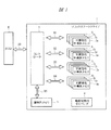
図1は、本発明の一実施の形態によるソリッドステートドライブの構成例を示すブロック図、図2は、図1のソリッドステートドライブに設けられた不揮発性半導体メモリのメモリアレイの構成例を示す説明図、図3は、図1のソリッドステートドライブに設けられたコントローラの構成例を示すブロック図、図4は、図1のソリッドステートドライブに設けられた不揮発性半導体メモリに格納されたブロック管理テーブルの構成例を示す説明図である。 FIG. 1 is a block diagram showing a configuration example of a solid state drive according to an embodiment of the present invention, and FIG. 2 is an explanation showing a configuration example of a memory array of a nonvolatile semiconductor memory provided in the solid state drive of FIG. 3 is a block diagram showing a configuration example of a controller provided in the solid state drive of FIG. 1, and FIG. 4 is a block management table stored in a nonvolatile semiconductor memory provided in the solid state drive of FIG. It is explanatory drawing which shows the example of a structure.
本実施の形態において、記憶装置であるソリッドステートドライブ1は、図1に示すように、たとえば、パーソナルコンピュータなどのホストHに内蔵されている記憶装置である。ホストHは、たとえば、ハードディスクドライブ互換の制御技術により、バスB0を介してソリッドステートドライブ1にデータの送受信を行う。
In the present embodiment, the solid-
ソリッドステートドライブ1は、コントローラ2、揮発性メモリ3、電源保持用キャパシタ4、および複数の不揮発性半導体メモリ51 〜54 ,61 〜64 ,71 〜74 ,81〜84 から構成されている。コントローラ2には、バスB1〜B4を介して、不揮発性半導体メモリ51 〜54 ,61 〜64 ,71 〜74 ,81 〜84 がそれぞれ接続されている。
The
また、コントローラ2には、バスB5を介して揮発性メモリ3が接続されている。コントローラ2は、ソリッドステートドライブ1の制御を司り、不揮発性半導体メモリ51 〜54 ,61 〜64 ,71 〜74 ,81 〜84 におけるデータの消去/書き込み/読み出し動作などを行う。
The
揮発性メモリ3は、たとえば、ホストHとの入出力データを一時的に保存するコントローラ2のキャッシュとして用いられる。さらに、揮発性メモリ3は、不揮発性半導体メモリ51 〜54 ,61 〜64 ,71 〜74 ,81 〜84 のユーザデータ領域を管理する管理データが記憶される。ユーザデータ領域は、ユーザがアクセス可能な記憶領域である。
The
電源遮断された際、揮発性メモリ3に記憶されている管理データ、およびキャッシュデータなどは、任意の不揮発性半導体メモリ51 〜54 ,61 〜64 ,71 〜74 ,81 〜84 にそれぞれ保存される。
When the power is shut off, the management data and cache data stored in the
電源保持用キャパシタ4は、一定時間、内部電源を保持し、コントローラ2、揮発性メモリ3、ならびに不揮発性半導体メモリ51 〜54 ,61 〜64 ,71 〜74 ,81 〜84 に電源を供給する。
The
不揮発性半導体メモリ51 〜54 ,61 〜64 ,71 〜74 ,81 〜84 は、ユーザデータなどをそれぞれ格納する。また、不揮発性半導体メモリ51 〜54 ,61 〜64 ,71 〜74 ,81 〜84 は、フラッシュメモリなどに例示される不揮発性半導体メモリであり、1つのメモリセルに2ビットのデータを書き込むMLCタイプとなっている。 The nonvolatile semiconductor memories 5 1 to 5 4 , 6 1 to 6 4 , 7 1 to 7 4 , and 8 1 to 8 4 store user data and the like, respectively. Non-volatile semiconductor memories 5 1 to 5 4 , 6 1 to 6 4 , 7 1 to 7 4 , and 8 1 to 8 4 are non-volatile semiconductor memories exemplified by a flash memory and the like. MLC type for writing 2-bit data.
不揮発性半導体メモリ51 〜54 ,61 〜64 ,71 〜74 ,81 〜84 は、前述したようにMLCタイプとなっているが、データは、消去単位であるブロック単位毎に2値でデータを格納する2値格納領域と多値でデータを格納する多値格納領域とに分割されて格納される。 The nonvolatile semiconductor memories 5 1 to 5 4 , 6 1 to 6 4 , 7 1 to 7 4 , and 8 1 to 8 4 are of the MLC type as described above, but the data is a block unit that is an erase unit. Each is divided and stored in a binary storage area for storing data in binary and a multi-value storage area for storing data in multiple values.
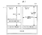
図2は、不揮発性半導体メモリ51 におけるメモリアレイの構成例を示す説明図である。なお、図2では、不揮発性半導体メモリ51 について説明するが、他の不揮発性半導体メモリ52 〜54 ,61 〜64 ,71 〜74 ,81 〜84 についても同様の構成となっている。 Figure 2 is an explanatory diagram showing a configuration example of a memory array in the nonvolatile semiconductor memory 5 1. In FIG. 2, it will be described non-volatile semiconductor memory 5 1, other non-volatile semiconductor memory 5 2-5 4, 61 through 4, 7 1-7 4, 8 1-8 4 same applies It has a configuration.
不揮発性半導体メモリ51 は、図示するように、1Gビット(2値)のメモリマットMT1,MT2が設けられている。メモリマットMT1,MT2は、ワード線数が32K本、ワード線数サイズが4K本にそれぞれ構成されている。 The nonvolatile semiconductor memory 5 1, as illustrated, the memory mats MT1, MT2 of 1G bit (binary) are provided. The memory mats MT1 and MT2 are configured so that the number of word lines is 32K and the number of word lines is 4K.
消去単位であるブロックサイズは、2値の場合には128KBとなっており、多値の場合には256KBとなっている。 The block size, which is an erasing unit, is 128 KB in the case of binary, and 256 KB in the case of multiple values.
不揮発性半導体メモリ51 は、1ワード線を上位ワード線と下位ワード線との2ワード化してあり、見かけ上ワード線を2倍としている。そして、2ビット以上のデータを格納する多値として用いる場合には、上位ワード線、および下位ワード線の両方を使用し、1ビットのデータを格納する2値として用いる場合には、2ワード化してあるワード線の上位ワード線のみを使用する。 The nonvolatile semiconductor memory 5 1 Yes and 2 words of an upper word line and the lower word lines one word line, and twice the apparent word line. When using as multiple values for storing data of 2 bits or more, both the upper word line and the lower word line are used, and when using as binary values for storing 1-bit data, it is converted into two words. Only the upper word line of a certain word line is used.
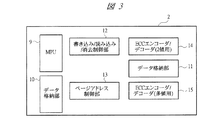
図3は、コントローラ2の構成例を示すブロック図である。
FIG. 3 is a block diagram illustrating a configuration example of the
コントローラ2は、図示するように、MPU(Micro Processing Unit)9、データ格納部10,11、書き込み/読み込み/消去制御部12、ページアドレス制御部13、およびECCエンコーダ/デコーダ14,15から構成されている。
The
MPU9は、コントローラ2におけるすべての制御を司る。データ格納部10は、バッファであり、ホストHとの送受信データを一時的に格納する。データ格納部11は、バッファであり、不揮発性半導体メモリへの書き込み/読み込みデータを一時的に格納する。
The MPU 9 manages all the controls in the
書き込み/読み込み/消去制御部12は、MPU9の制御に基づいて、任意の不揮発性半導体メモリ51 〜54 ,61 〜64 ,71 〜74 ,81 〜84 にデータの書き込み/読み込み/消去を行う。
The write / read /
ページアドレス制御部13は、ブロック管理テーブルBT(図4)を参照し、ページアドレスの制御を行う。ECCエンコーダ/デコーダ14は、2値のデータに対してのECCの付加や、データ訂正処理を行う。ECCエンコーダ/デコーダ15は、多値のデータに対してのECCを付加や、データ訂正処理を行う。
The page
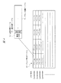
図4は、ブロック管理テーブルBTの構成例を示す説明図である。 FIG. 4 is an explanatory diagram showing a configuration example of the block management table BT.
ブロック管理テーブルBTは、回数管理テーブルT1、2値/多値テーブルT2、およびアドレス変換テーブルT3などから構成されており、これらの管理情報がブロック番号毎に格納されている。 The block management table BT includes a number management table T1, a binary / multilevel table T2, an address conversion table T3, and the like, and these pieces of management information are stored for each block number.
回数管理テーブルT1は、そのブロックの書き換え回数を示すテーブルであり、2値/多値テーブルT2は、そのブロックが2値、多値のどちらで使われるかを示すテーブルである。 The number management table T1 is a table indicating the number of rewrites of the block, and the binary / multilevel table T2 is a table indicating whether the block is used in binary or multivalue.
ブロック管理テーブルBTは、不揮発性半導体メモリ51 〜54 ,61 〜64 ,71 〜74 ,81 〜84 のシステム領域にそれぞれ格納される。システム領域は、ユーザがアクセス不可の記憶領域である。 The block management table BT is stored in the system areas of the nonvolatile semiconductor memories 5 1 to 5 4 , 6 1 to 6 4 , 7 1 to 7 4 , and 8 1 to 8 4 , respectively. The system area is a storage area that cannot be accessed by the user.
2値/多値テーブルT2の初期値は、たとえば、ユーザデータ領域のすべてのブロックを多値で使用するように設定されており、システム領域のブロックは、2値で使用するように設定されている。 The initial values of the binary / multi-value table T2 are set so that all blocks in the user data area are used in multi-value, for example, and the blocks in the system area are set to be used in binary. Yes.
このように、ブロック管理テーブルBTなどの書き換え頻度が高く、信頼性が求められるデータを2値で記憶することにより、ソリッドステートドライブ1の信頼性をより向上させることができる。
As described above, the reliability of the solid-
また、アドレス変換テーブルT3は、ホストHから指定された論理アドレスから、不揮発性半導体メモリの物理アドレスへの変換を管理するテーブルである。 The address conversion table T3 is a table for managing the conversion from the logical address designated by the host H to the physical address of the nonvolatile semiconductor memory.
不揮発性半導体メモリ51 〜54 ,61 〜64 ,71 〜74 ,81 〜84 には、前述した管理データを記憶するシステム領域、ユーザデータを格納するユーザデータ領域、ならびに該ユーザデータ領域の代替となり、代替記憶領域として用いられる予備領域が備えられている。 The non-volatile semiconductor memories 5 1 to 5 4 , 6 1 to 6 4 , 7 1 to 7 4 , and 8 1 to 8 4 each include a system area for storing the management data, a user data area for storing user data, and A spare area used as an alternative storage area is provided instead of the user data area.
そして、ユーザデータ領域のあるブロックに不良が発生した際には、コントローラ2が、その不良ブロックの代替として予備領域のあるブロックを使用する代替処理を行う。
When a failure occurs in a block having a user data area, the
ブロック番号は、不揮発性半導体メモリ51 〜54 ,61 〜64 ,71 〜74 ,81 〜84 におけるすべて領域(システム領域、ユーザデータ領域、および予備領域)のブロックに対して通し番号となるブロック番号’0’〜’N’となっている。 Block numbers are assigned to blocks in all areas (system area, user data area, and spare area) in the nonvolatile semiconductor memories 5 1 to 5 4 , 6 1 to 6 4 , 7 1 to 7 4 , and 8 1 to 8 4 . The block numbers “0” to “N” are serial numbers.
ブロック管理テーブルBTは、電源遮断時には、不揮発性半導体メモリ51 〜54 ,61 〜64 ,71 〜74 ,81 〜84 のシステム領域にそれぞれ格納されており、ソリッドステートドライブ1が動作した際に揮発性メモリ3に展開される。
The block management table BT is stored in the system areas of the non-volatile semiconductor memories 5 1 to 5 4 , 6 1 to 6 4 , 7 1 to 7 4 , and 8 1 to 8 4 when the power is turned off. 1 is expanded in the
次に、本実施の形態によるソリッドステートドライブ1の動作について説明する。
Next, the operation of the
まず、ホストHから送信されたデータは、バッファであるデータ格納部10に一時的に格納される。このとき、回数管理テーブルT1の該当ブロックの書き換え回数が任意の設定値以上であれば、MPU9により該当ブロックの2値/多値テーブルT2が多値から2値として使用するように更新される。
First, data transmitted from the host H is temporarily stored in the
データ格納部10に格納されたデータは、ECCエンコーダ/デコーダ15(またはECCエンコーダ/デコーダ14)によってECCが付加された後、揮発性メモリ3に格納される。
The data stored in the
ECCエンコーダ/デコーダ14、またはECCエンコーダ/デコーダ15の選択は、書き込み/読み込み/消去制御部12がブロック管理テーブルBT(図4)の2値/多値テーブルT2を参照することにより決定される。
The selection of the ECC encoder /
前述したように、初期設定では、ユーザデータ領域のブロックが多値としてデータが格納されるように2値/多値テーブルT2が設定されているが、回数管理テーブルT1の書き換え回数が任意の設定値以上となっている場合には、2値としてデータが格納されるように2値/多値テーブルT2の設定変更が行われる。 As described above, in the initial setting, the binary / multi-value table T2 is set so that data is stored as multi-valued blocks in the user data area, but the number of rewrites of the number management table T1 can be arbitrarily set. If the value is greater than or equal to the value, the setting of the binary / multi-value table T2 is changed so that the data is stored as a binary value.
続いて、MPU9は、揮発性メモリ3におけるデータキャッシュ領域の状態から、書き込み/読み込み/消去制御部12に任意の不揮発性半導体メモリへの書き込み指示を行い、揮発性メモリ3に格納されたデータがデータ格納部11に格納される。
Subsequently, the MPU 9 instructs the write / read / erase
このとき、ページアドアドレス制御部13は、ブロック管理テーブルBTを参照し、2値/多値のいずれになるかを確認し、アドレス制御を行う。続いて、書き込み/読み込み/消去制御部12は、MPU9が設定した選択ビット値を参照して選択された任意のブロックにデータの書き込みを行う。
At this time, the page add
データ書き込みが終了すると、MPU9は、ブロック管理テーブルBTの回数管理テーブルT1の書き換えを行う。 When the data writing is completed, the MPU 9 rewrites the number management table T1 of the block management table BT.
また、任意のブロックからデータを読み出す場合、読み出されたデータは、データ格納部11に格納され、ECCエンコーダ/デコーダ15(またはECCエンコーダ/デコーダ14)によりデータ訂正処理が行われた後、揮発性メモリ3に該データが格納される。
When data is read from an arbitrary block, the read data is stored in the
さらに、書き込み/読み出し/消去制御部12は、データの書き込み、または読み出し時にFAIL(エラー)となると、FAILとなったそのブロックのデータを書き換えの際に予備領域に設けられた任意のブロックに書き込むように制御を行う。
Further, when a FAIL (error) occurs at the time of data writing or reading, the writing / reading / erasing
次に、ECCエンコーダ/デコーダ14,15が付加するデータ訂正用のECCビット数について説明する。
Next, the number of ECC bits for data correction added by the ECC encoder /
多値ブロックのデータ訂正用ECCビットを付加するECCエンコーダ/デコーダ15は、2値ブロックのデータ訂正用ECCビットを付加するECCエンコーダ/デコーダ14のECCビット数(たとえば、4ビット程度)よりも、付加するECCビット数(たとえば、6ビット程度)が多くなる構成となっている。
The ECC encoder /
これにより、多値ブロックに記憶されるデータの信頼性を向上させ、2値ブロックに記憶されるデータと多値ブロックに記憶されるデータとの間の信頼性の差を少なくすることが可能となる。 As a result, it is possible to improve the reliability of data stored in the multi-value block and reduce the difference in reliability between the data stored in the binary block and the data stored in the multi-value block. Become.
それにより、本実施の形態によれば、ユーザデータ領域に格納されるデータを多値で記憶し、データの書き換えが頻繁に行われるシステム領域のデータを2値で記憶させることにより、低コストで信頼性の高い、大記憶容量のソリッドステートドライブ1を実現することができる。
Thus, according to the present embodiment, the data stored in the user data area is stored in multiple values, and the data in the system area in which data is frequently rewritten is stored in binary. A highly reliable
また、前記実施の形態では、2値/多値テーブルT2の初期値は、たとえば、ユーザデータ領域のすべてのブロックを多値で使用するように設定し、システム領域のブロックを2値で使用するように設定する場合について記載したが、この初期設定は、任意に設定可能である。 In the above embodiment, the initial value of the binary / multi-value table T2 is set so that, for example, all blocks in the user data area are used in multiple values, and the blocks in the system area are used in binary values. Although the case of setting as described above has been described, this initial setting can be arbitrarily set.
たとえば、システム領域のブロックだけでなく、ユーザデータ領域における任意のブロックを2値で使用し、その他のブロックを多値で使用するようにしてもよいし、あるいは、すべてのブロックを2値や多値で使用するようにしてもよい。 For example, not only blocks in the system area but also arbitrary blocks in the user data area may be used as binary values, and other blocks may be used as multiple values, or all blocks may be binary or multiple. You may make it use by a value.
前述したユーザデータ領域における任意のブロックを2値で使用する場合、この2値で使用されるブロックに電源遮断の際に揮発性メモリ3のユーザデータを書き込む記憶領域として使用する。
When an arbitrary block in the user data area described above is used in binary, the block used in binary is used as a storage area for writing user data in the
これにより、より高速にソリッドステートドライブ1の電源遮断することができる。これは、不揮発性半導体メモリを消去のブロック単位で分割した際に、上位ワード線は、下位ワード線よりもデータの書き込み速度が速くなるので、2値で使用するブロックは、多値で使用するブロックよりもデータ書き込み速度が速くなるためである。
Thereby, the power supply of the
以上、本発明者によってなされた発明を実施の形態に基づき具体的に説明したが、本発明は前記実施の形態に限定されるものではなく、その要旨を逸脱しない範囲で種々変更可能であることはいうまでもない。 As mentioned above, the invention made by the present inventor has been specifically described based on the embodiment. However, the present invention is not limited to the embodiment, and various modifications can be made without departing from the scope of the invention. Needless to say.
本発明は、不揮発性半導体メモリを用いた記憶装置に適している。 The present invention is suitable for a storage device using a nonvolatile semiconductor memory.
1 ソリッドステートドライブ
2 コントローラ
3 揮発性メモリ
4 電源保持用キャパシタ
51 〜54 不揮発性半導体メモリ
61 〜64 不揮発性半導体メモリ
71 〜74 不揮発性半導体メモリ
81 〜84 不揮発性半導体メモリ
9 MPU
10,11 データ格納部
12 書き込み/読み込み/消去制御部
13 ページアドレス制御部
14,15 ECCエンコーダ/デコーダ
H ホスト
B0〜B5 バス
MT1,MT2 メモリマット
BT ブロック管理テーブル
T1 回数管理テーブル
T2 2値/多値テーブル
T3 アドレス変換テーブル
1
10, 11
Claims (2)
ある電圧レベルのしきい値を複数設定し2ビット以上の多値でデータ書き込みが可能にされた不揮発性半導体メモリセルのメモリアレイで構成された不揮発性半導体メモリと、
揮発性メモリと、
前記ホストから発行されたコマンドに基づいて前記不揮発性半導体メモリの動作指示を行うコントローラと、
電源保持用キャパシタとを備え、
前記不揮発性半導体メモリは、前記多値書き込み可能な不揮発性半導体メモリセルが2値(1ビット)でデータ書き込みが行われるブロックとして制御される領域(以下「2値ブロック」という。)と、前記多値でデータ書き込みが行われるブロックとして制御される領域(以下「多値ブロック」という。)で構成され、ユーザのアクセスが不可とされるシステム領域のデータは前記2値ブロックに格納され、ユーザデータ領域のデータは前記多値ブロックに格納されるように設定されており、
前記多値書き込み可能な不揮発性半導体メモリセルのブロックを2値ブロックとしてデータを格納するか多値ブロックとしてデータを格納するかを示す2値/多値書き込み情報を有したブロック管理テーブルが前記2値ブロックのシステム領域に格納されており、
前記コントローラは、
前記記憶装置の動作時に前記ブロック管理テーブルを前記揮発性メモリに展開する処理と、
前記不揮発性半導体メモリの書き換え耐数に至る前の処理において、ホストから送信されるデータを前記ブロック管理テーブルの2値/多値書き込み情報を参照して前記2値ブロックに格納するデータか前記多値ブロックに格納するデータかを決定し、前記不揮発性半導体メモリにデータを書き込む処理と、
電源遮断が発生したときは、前記電源保持用キャパシタから供給される電源によって、前記揮発性メモリに一時記憶されているユーザデータを前記2値ブロックに書き込む処理とを実行するように構成されてなることを特徴とする記憶装置。 A storage device composed of a nonvolatile semiconductor memory and configured to be controllable by a hard disk drive compatible control technology from a host,
A non-volatile semiconductor memory configured with a memory array of non-volatile semiconductor memory cells in which a plurality of threshold values of a certain voltage level are set and data can be written in multiple values of 2 bits or more;
Volatile memory,
A controller for instructing operation of the nonvolatile semiconductor memory based on a command issued from the host;
A power holding capacitor,
The non-volatile semiconductor memory is an area (hereinafter referred to as “binary block”) in which the multi-value writable non-volatile semiconductor memory cell is controlled as a block in which data is written in binary (1 bit). Data in the system area, which is composed of an area controlled as a block where multi-value data is written (hereinafter referred to as “multi-value block”) and which cannot be accessed by the user, is stored in the binary block. Data area data is set to be stored in the multi-value block,
A block management table having binary / multi-level write information indicating whether data is stored as a binary block or data as a multi-level block is stored in the block of the multi-level writable nonvolatile semiconductor memory cell. Stored in the system area of the value block,
The controller is
Processing for expanding the block management table in the volatile memory during operation of the storage device;
In the processing before reaching the rewrite tolerance of the nonvolatile semiconductor memory, the data transmitted from the host is stored in the binary block with reference to the binary / multi-value write information of the block management table. Determining whether to store data in a value block, and writing data to the nonvolatile semiconductor memory;
When a power interruption occurs, a process of writing user data temporarily stored in the volatile memory into the binary block is executed by the power supplied from the power holding capacitor. A storage device.
Priority Applications (1)
| Application Number | Priority Date | Filing Date | Title |
|---|---|---|---|
| JP2007211741A JP5259138B2 (en) | 2007-08-15 | 2007-08-15 | Storage device |
Applications Claiming Priority (1)
| Application Number | Priority Date | Filing Date | Title |
|---|---|---|---|
| JP2007211741A JP5259138B2 (en) | 2007-08-15 | 2007-08-15 | Storage device |
Publications (2)
| Publication Number | Publication Date |
|---|---|
| JP2009048680A JP2009048680A (en) | 2009-03-05 |
| JP5259138B2 true JP5259138B2 (en) | 2013-08-07 |
Family
ID=40500758
Family Applications (1)
| Application Number | Title | Priority Date | Filing Date |
|---|---|---|---|
| JP2007211741A Expired - Fee Related JP5259138B2 (en) | 2007-08-15 | 2007-08-15 | Storage device |
Country Status (1)
| Country | Link |
|---|---|
| JP (1) | JP5259138B2 (en) |
Cited By (1)
| Publication number | Priority date | Publication date | Assignee | Title |
|---|---|---|---|---|
| CN104919434A (en) * | 2012-12-07 | 2015-09-16 | 西部数据技术公司 | System and method for lower page data recovery in a solid state drive |
Families Citing this family (10)
| Publication number | Priority date | Publication date | Assignee | Title |
|---|---|---|---|---|
| JP5612508B2 (en) | 2010-03-25 | 2014-10-22 | パナソニック株式会社 | Nonvolatile memory controller and nonvolatile storage device |
| JP5533141B2 (en) * | 2010-03-31 | 2014-06-25 | アイシン・エィ・ダブリュ株式会社 | Writing device, writing method, and writing program |
| JP2012203863A (en) | 2011-03-28 | 2012-10-22 | Toshiba Corp | Memory system |
| JP2015138498A (en) * | 2014-01-24 | 2015-07-30 | 三菱電機株式会社 | Flash memory error correction coding apparatus and method |
| JP6146675B2 (en) | 2014-06-03 | 2017-06-14 | コニカミノルタ株式会社 | Image forming apparatus, flash memory control method, and control program |
| JP2016004387A (en) * | 2014-06-16 | 2016-01-12 | 株式会社東芝 | Storage system, memory controller, and control method |
| JP6493355B2 (en) * | 2016-10-14 | 2019-04-03 | 京セラドキュメントソリューションズ株式会社 | Memory system and image forming apparatus |
| JP2018160303A (en) * | 2017-03-23 | 2018-10-11 | 東芝メモリ株式会社 | Semiconductor storage device |
| JP7039348B2 (en) * | 2018-03-20 | 2022-03-22 | キオクシア株式会社 | Write control device, storage device, network system, and write control method |
| KR20230068197A (en) | 2021-11-10 | 2023-05-17 | 삼성전자주식회사 | Storate device and operating method of the same |
Family Cites Families (3)
| Publication number | Priority date | Publication date | Assignee | Title |
|---|---|---|---|---|
| JPH11283396A (en) * | 1998-03-27 | 1999-10-15 | Sony Corp | Memory device |
| JP2000298992A (en) * | 1999-04-13 | 2000-10-24 | Hitachi Ltd | Control device for multi-value storage nonvolatile semiconductor memory |
| JP2001306393A (en) * | 2000-04-20 | 2001-11-02 | Mitsubishi Electric Corp | Storage device |
-
2007
- 2007-08-15 JP JP2007211741A patent/JP5259138B2/en not_active Expired - Fee Related
Cited By (1)
| Publication number | Priority date | Publication date | Assignee | Title |
|---|---|---|---|---|
| CN104919434A (en) * | 2012-12-07 | 2015-09-16 | 西部数据技术公司 | System and method for lower page data recovery in a solid state drive |
Also Published As
| Publication number | Publication date |
|---|---|
| JP2009048680A (en) | 2009-03-05 |
Similar Documents
| Publication | Publication Date | Title |
|---|---|---|
| JP5259138B2 (en) | Storage device | |
| US9996274B2 (en) | Flash memory system | |
| US9292428B2 (en) | Memory system | |
| US7974139B2 (en) | Non-volatile memory generating different read voltages | |
| US20160070507A1 (en) | Memory system and method of controlling memory device | |
| US20170091039A1 (en) | Data storage device and operating method thereof | |
| US8694748B2 (en) | Data merging method for non-volatile memory module, and memory controller and memory storage device using the same | |
| KR20080067834A (en) | Programmable memory system | |
| CN115145755B (en) | System and method for remapping bad blocks in a memory subsystem | |
| CN113808656B (en) | Bad growth block management in a memory subsystem | |
| CN111352854B (en) | Storage device, controller and method of operating storage device | |
| US11847065B2 (en) | Memory sub-system management of firmware block record and device block record | |
| US9122583B2 (en) | Memory controller and memory storage device and data writing method | |
| CN115437558A (en) | Diagonal page mapping in a memory system | |
| US9728264B2 (en) | Nonvolatile memory device, operating method thereof, and data storage device including the same | |
| US11222693B2 (en) | Data management method for memory and memory apparatus using the same | |
| CN117435519B (en) | Buffer allocation for reducing block transfer losses | |
| CN115732003A (en) | Memory subsystem scrubbing | |
| US20130286731A1 (en) | Memory device, memory control device, and memory control method | |
| US12062394B2 (en) | Performing data integrity checks to identify defective wordlines | |
| US12299282B2 (en) | Runtime storage capacity reduction avoidance in sequentially-written memory devices | |
| US20250208992A1 (en) | Wordline group-based identification of good memory blocks during a programming operation | |
| US20260037431A1 (en) | Storage device and method of operating the same | |
| US20240192875A1 (en) | Remapping bad blocks in a memory sub-system | |
| CN115079928B (en) | Jumping data clearing method and data storage system |
Legal Events
| Date | Code | Title | Description |
|---|---|---|---|
| A621 | Written request for application examination |
Free format text: JAPANESE INTERMEDIATE CODE: A621 Effective date: 20100203 |
|
| A977 | Report on retrieval |
Free format text: JAPANESE INTERMEDIATE CODE: A971007 Effective date: 20120222 |
|
| A131 | Notification of reasons for refusal |
Free format text: JAPANESE INTERMEDIATE CODE: A131 Effective date: 20120321 |
|
| A521 | Written amendment |
Free format text: JAPANESE INTERMEDIATE CODE: A523 Effective date: 20120518 |
|
| A02 | Decision of refusal |
Free format text: JAPANESE INTERMEDIATE CODE: A02 Effective date: 20121106 |
|
| A521 | Written amendment |
Free format text: JAPANESE INTERMEDIATE CODE: A523 Effective date: 20130205 |
|
| A911 | Transfer of reconsideration by examiner before appeal (zenchi) |
Free format text: JAPANESE INTERMEDIATE CODE: A911 Effective date: 20130212 |
|
| TRDD | Decision of grant or rejection written | ||
| A01 | Written decision to grant a patent or to grant a registration (utility model) |
Free format text: JAPANESE INTERMEDIATE CODE: A01 Effective date: 20130402 |
|
| A61 | First payment of annual fees (during grant procedure) |
Free format text: JAPANESE INTERMEDIATE CODE: A61 Effective date: 20130424 |
|
| FPAY | Renewal fee payment (event date is renewal date of database) |
Free format text: PAYMENT UNTIL: 20160502 Year of fee payment: 3 |
|
| R150 | Certificate of patent or registration of utility model |
Free format text: JAPANESE INTERMEDIATE CODE: R150 |
|
| LAPS | Cancellation because of no payment of annual fees |