JP5250737B2 - Liquid crystal display device and driving method thereof - Google Patents
Liquid crystal display device and driving method thereof Download PDFInfo
- Publication number
- JP5250737B2 JP5250737B2 JP2007251317A JP2007251317A JP5250737B2 JP 5250737 B2 JP5250737 B2 JP 5250737B2 JP 2007251317 A JP2007251317 A JP 2007251317A JP 2007251317 A JP2007251317 A JP 2007251317A JP 5250737 B2 JP5250737 B2 JP 5250737B2
- Authority
- JP
- Japan
- Prior art keywords
- liquid crystal
- voltage
- electrode
- display device
- crystal display
- Prior art date
- Legal status (The legal status is an assumption and is not a legal conclusion. Google has not performed a legal analysis and makes no representation as to the accuracy of the status listed.)
- Expired - Fee Related
Links
Images

Classifications
-
- G—PHYSICS
- G02—OPTICS
- G02F—OPTICAL DEVICES OR ARRANGEMENTS FOR THE CONTROL OF LIGHT BY MODIFICATION OF THE OPTICAL PROPERTIES OF THE MEDIA OF THE ELEMENTS INVOLVED THEREIN; NON-LINEAR OPTICS; FREQUENCY-CHANGING OF LIGHT; OPTICAL LOGIC ELEMENTS; OPTICAL ANALOGUE/DIGITAL CONVERTERS
- G02F1/00—Devices or arrangements for the control of the intensity, colour, phase, polarisation or direction of light arriving from an independent light source, e.g. switching, gating or modulating; Non-linear optics
- G02F1/01—Devices or arrangements for the control of the intensity, colour, phase, polarisation or direction of light arriving from an independent light source, e.g. switching, gating or modulating; Non-linear optics for the control of the intensity, phase, polarisation or colour
- G02F1/13—Devices or arrangements for the control of the intensity, colour, phase, polarisation or direction of light arriving from an independent light source, e.g. switching, gating or modulating; Non-linear optics for the control of the intensity, phase, polarisation or colour based on liquid crystals, e.g. single liquid crystal display cells
- G02F1/133—Constructional arrangements; Operation of liquid crystal cells; Circuit arrangements
-
- G—PHYSICS
- G09—EDUCATION; CRYPTOGRAPHY; DISPLAY; ADVERTISING; SEALS
- G09G—ARRANGEMENTS OR CIRCUITS FOR CONTROL OF INDICATING DEVICES USING STATIC MEANS TO PRESENT VARIABLE INFORMATION
- G09G3/00—Control arrangements or circuits, of interest only in connection with visual indicators other than cathode-ray tubes
- G09G3/20—Control arrangements or circuits, of interest only in connection with visual indicators other than cathode-ray tubes for presentation of an assembly of a number of characters, e.g. a page, by composing the assembly by combination of individual elements arranged in a matrix no fixed position being assigned to or needed to be assigned to the individual characters or partial characters
- G09G3/34—Control arrangements or circuits, of interest only in connection with visual indicators other than cathode-ray tubes for presentation of an assembly of a number of characters, e.g. a page, by composing the assembly by combination of individual elements arranged in a matrix no fixed position being assigned to or needed to be assigned to the individual characters or partial characters by control of light from an independent source
- G09G3/36—Control arrangements or circuits, of interest only in connection with visual indicators other than cathode-ray tubes for presentation of an assembly of a number of characters, e.g. a page, by composing the assembly by combination of individual elements arranged in a matrix no fixed position being assigned to or needed to be assigned to the individual characters or partial characters by control of light from an independent source using liquid crystals
- G09G3/3611—Control of matrices with row and column drivers
- G09G3/3648—Control of matrices with row and column drivers using an active matrix
- G09G3/3655—Details of drivers for counter electrodes, e.g. common electrodes for pixel capacitors or supplementary storage capacitors
-
- G—PHYSICS
- G02—OPTICS
- G02F—OPTICAL DEVICES OR ARRANGEMENTS FOR THE CONTROL OF LIGHT BY MODIFICATION OF THE OPTICAL PROPERTIES OF THE MEDIA OF THE ELEMENTS INVOLVED THEREIN; NON-LINEAR OPTICS; FREQUENCY-CHANGING OF LIGHT; OPTICAL LOGIC ELEMENTS; OPTICAL ANALOGUE/DIGITAL CONVERTERS
- G02F1/00—Devices or arrangements for the control of the intensity, colour, phase, polarisation or direction of light arriving from an independent light source, e.g. switching, gating or modulating; Non-linear optics
- G02F1/01—Devices or arrangements for the control of the intensity, colour, phase, polarisation or direction of light arriving from an independent light source, e.g. switching, gating or modulating; Non-linear optics for the control of the intensity, phase, polarisation or colour
- G02F1/13—Devices or arrangements for the control of the intensity, colour, phase, polarisation or direction of light arriving from an independent light source, e.g. switching, gating or modulating; Non-linear optics for the control of the intensity, phase, polarisation or colour based on liquid crystals, e.g. single liquid crystal display cells
- G02F1/133—Constructional arrangements; Operation of liquid crystal cells; Circuit arrangements
- G02F1/1333—Constructional arrangements; Manufacturing methods
- G02F1/1337—Surface-induced orientation of the liquid crystal molecules, e.g. by alignment layers
-
- G—PHYSICS
- G09—EDUCATION; CRYPTOGRAPHY; DISPLAY; ADVERTISING; SEALS
- G09G—ARRANGEMENTS OR CIRCUITS FOR CONTROL OF INDICATING DEVICES USING STATIC MEANS TO PRESENT VARIABLE INFORMATION
- G09G2300/00—Aspects of the constitution of display devices
- G09G2300/04—Structural and physical details of display devices
- G09G2300/0469—Details of the physics of pixel operation
- G09G2300/0478—Details of the physics of pixel operation related to liquid crystal pixels
- G09G2300/0491—Use of a bi-refringent liquid crystal, optically controlled bi-refringence [OCB] with bend and splay states, or electrically controlled bi-refringence [ECB] for controlling the color
-
- G—PHYSICS
- G09—EDUCATION; CRYPTOGRAPHY; DISPLAY; ADVERTISING; SEALS
- G09G—ARRANGEMENTS OR CIRCUITS FOR CONTROL OF INDICATING DEVICES USING STATIC MEANS TO PRESENT VARIABLE INFORMATION
- G09G2310/00—Command of the display device
- G09G2310/02—Addressing, scanning or driving the display screen or processing steps related thereto
- G09G2310/0243—Details of the generation of driving signals
- G09G2310/0245—Clearing or presetting the whole screen independently of waveforms, e.g. on power-on
-
- G—PHYSICS
- G09—EDUCATION; CRYPTOGRAPHY; DISPLAY; ADVERTISING; SEALS
- G09G—ARRANGEMENTS OR CIRCUITS FOR CONTROL OF INDICATING DEVICES USING STATIC MEANS TO PRESENT VARIABLE INFORMATION
- G09G2310/00—Command of the display device
- G09G2310/06—Details of flat display driving waveforms
-
- G—PHYSICS
- G09—EDUCATION; CRYPTOGRAPHY; DISPLAY; ADVERTISING; SEALS
- G09G—ARRANGEMENTS OR CIRCUITS FOR CONTROL OF INDICATING DEVICES USING STATIC MEANS TO PRESENT VARIABLE INFORMATION
- G09G2310/00—Command of the display device
- G09G2310/06—Details of flat display driving waveforms
- G09G2310/066—Waveforms comprising a gently increasing or decreasing portion, e.g. ramp
-
- G—PHYSICS
- G09—EDUCATION; CRYPTOGRAPHY; DISPLAY; ADVERTISING; SEALS
- G09G—ARRANGEMENTS OR CIRCUITS FOR CONTROL OF INDICATING DEVICES USING STATIC MEANS TO PRESENT VARIABLE INFORMATION
- G09G2330/00—Aspects of power supply; Aspects of display protection and defect management
- G09G2330/02—Details of power systems and of start or stop of display operation
- G09G2330/026—Arrangements or methods related to booting a display
-
- G—PHYSICS
- G09—EDUCATION; CRYPTOGRAPHY; DISPLAY; ADVERTISING; SEALS
- G09G—ARRANGEMENTS OR CIRCUITS FOR CONTROL OF INDICATING DEVICES USING STATIC MEANS TO PRESENT VARIABLE INFORMATION
- G09G3/00—Control arrangements or circuits, of interest only in connection with visual indicators other than cathode-ray tubes
- G09G3/20—Control arrangements or circuits, of interest only in connection with visual indicators other than cathode-ray tubes for presentation of an assembly of a number of characters, e.g. a page, by composing the assembly by combination of individual elements arranged in a matrix no fixed position being assigned to or needed to be assigned to the individual characters or partial characters
- G09G3/34—Control arrangements or circuits, of interest only in connection with visual indicators other than cathode-ray tubes for presentation of an assembly of a number of characters, e.g. a page, by composing the assembly by combination of individual elements arranged in a matrix no fixed position being assigned to or needed to be assigned to the individual characters or partial characters by control of light from an independent source
- G09G3/36—Control arrangements or circuits, of interest only in connection with visual indicators other than cathode-ray tubes for presentation of an assembly of a number of characters, e.g. a page, by composing the assembly by combination of individual elements arranged in a matrix no fixed position being assigned to or needed to be assigned to the individual characters or partial characters by control of light from an independent source using liquid crystals
- G09G3/3611—Control of matrices with row and column drivers
- G09G3/3614—Control of polarity reversal in general
Landscapes
- Physics & Mathematics (AREA)
- Engineering & Computer Science (AREA)
- General Physics & Mathematics (AREA)
- Crystallography & Structural Chemistry (AREA)
- Chemical & Material Sciences (AREA)
- Nonlinear Science (AREA)
- Computer Hardware Design (AREA)
- Power Engineering (AREA)
- Theoretical Computer Science (AREA)
- Mathematical Physics (AREA)
- Optics & Photonics (AREA)
- Liquid Crystal (AREA)
- Spectroscopy & Molecular Physics (AREA)
- Control Of Indicators Other Than Cathode Ray Tubes (AREA)
- Liquid Crystal Display Device Control (AREA)
Description
本発明は液晶表示装置、特に、OCB(Optically Compensated Bend)方式の液晶表示装置に関する。 The present invention relates to a liquid crystal display device, and more particularly to an OCB (Optically Compensated Bend) type liquid crystal display device.
液晶表示装置は、現在最も広く使用されている平板表示装置のうちの1つであって、画素電極と共通電極など電場生成電極が形成されている2枚の表示板とその間に入っている液晶層を含む。液晶表示装置は、電場生成電極に電圧を印加して液晶層に電場を生成して、これを通じて液晶層の液晶分子の方向を決定して入射光の偏光を制御することによって映像を表示する。 The liquid crystal display device is one of the most widely used flat panel display devices, and includes two display plates on which electric field generating electrodes such as a pixel electrode and a common electrode are formed, and a liquid crystal interposed therebetween. Including layers. The liquid crystal display device displays an image by applying a voltage to the electric field generating electrode to generate an electric field in the liquid crystal layer, thereby determining the direction of liquid crystal molecules in the liquid crystal layer and controlling the polarization of incident light.
このような液晶表示装置の中で、応答速度及び基準視野角を改善するために多様な方法が提示され、例えば、OCB方式の液晶表示装置を挙げることができる。
このようなOCB方式の液晶表示装置では2つの電場生成電極に電場が印加された時液晶分子が2つの表示板の間の中心面に対して対称でありながら表示板面から中心面に至るまで水平配列から垂直配列に変わるので広い基準視野角を得ることができる。
Among such liquid crystal display devices, various methods have been proposed to improve the response speed and the reference viewing angle. For example, an OCB type liquid crystal display device can be given.
In such an OCB type liquid crystal display device, when an electric field is applied to two electric field generating electrodes, the liquid crystal molecules are symmetrical with respect to the central plane between the two display panels, but horizontally aligned from the display panel surface to the central plane. Since the vertical arrangement is changed, a wide reference viewing angle can be obtained.
しかしながら、OCB方式の液晶表示装置は他の液晶モードとは異なって安定な状態ではなくて、電圧を全く印加しない状態ではスプレイ配向を有し、これをベンド配向に転移させなければならない。 However, the OCB type liquid crystal display device is not in a stable state unlike other liquid crystal modes, and has a splay alignment in a state where no voltage is applied, and must be transferred to a bend alignment.
本発明の課題は、電源供給時の短時間内にスプレイ配向からベンド配向に転移させることができるOCB液晶表示装置を提供することにある。 The subject of this invention is providing the OCB liquid crystal display device which can be changed from a splay alignment to a bend alignment within the short time at the time of power supply.
上記課題を解決するために、本発明の一実施例による液晶表示装置は第1基板、前記第1基板上に形成された第1電極、前記第1基板と対向する第2基板、前記第2基板上に形成されており、前記第1電極と対向する第2電極、前記第1及び第2電極の間に液晶を注入することにより形成された液晶層、前記第1電極に複数回にかけて電荷を供給することによって前記液晶の配向を転移させるベンド電圧を印加する複数の電荷供給部を含む。 In order to solve the above problems, a liquid crystal display device according to an embodiment of the present invention includes a first substrate, a first electrode formed on the first substrate, a second substrate facing the first substrate, and the second substrate. A second electrode formed on the substrate and facing the first electrode, a liquid crystal layer formed by injecting liquid crystal between the first and second electrodes, and a charge applied to the first electrode a plurality of times. And a plurality of charge supply units for applying a bend voltage for changing the alignment of the liquid crystal.
前記液晶の配向転移によって前記液晶の配向がスプレイ配向からベンド配向に変換するように構成できる。
前記電荷供給部は、前記液晶表示装置が映像を表示する前に前記ベンド電圧を前記第1電極に印加するように構成できる。
前記電荷供給部は、前記液晶表示装置が映像を表示する間前記第1電極に共通電圧を印加するように構成できる。
The liquid crystal alignment may be changed from a splay alignment to a bend alignment by the alignment transition of the liquid crystal.
The charge supply unit may be configured to apply the bend voltage to the first electrode before the liquid crystal display device displays an image.
The charge supply unit may be configured to apply a common voltage to the first electrode while the liquid crystal display device displays an image.
前記電荷供給部は、前記共通電圧と基準節点の間に接続されたキャパシタ、ベンド電圧と前記基準節点の間に接続された第1スイッチング素子、そして前記基準節点と前記第1電極の間に接続された第2スイッチング素子を含む構成とすることができる。
前記第1及び第2スイッチング素子は交互に導通するように構成できる。
前記ベンド電圧は前記共通電圧より高い電圧であってもよい。
The charge supply unit includes a capacitor connected between the common voltage and a reference node, a first switching element connected between a bend voltage and the reference node, and a connection between the reference node and the first electrode. It can be set as the structure containing the made 2nd switching element.
The first and second switching elements may be configured to conduct alternately.
The bend voltage may be higher than the common voltage.
前記電荷供給部は、前記共通電圧と前記第1電極の間に接続されている第3スイッチング素子を更に含み、前記第3スイッチング素子は前記第1電極が前記ベンド電圧で充電された後導通するように構成できる。
前記ベンド電圧は時間によって電圧レベルが上昇するように構成できる。
また、本発明の一実施例による液晶表示装置の駆動方法は第1基板、前記第1基板上に形成された第1電極、前記第1基板と対向する第2基板、前記第2基板上に形成されており、前記第1電極と対向する第2電極、そして前記第1及び第2電極の間に液晶を注入することにより形成された液晶層を含む液晶表示装置の駆動方法で、前記第1電極に複数回にかけて電荷を供給することによって前記液晶の配向を転移させるベンド電圧を印加する段階、前記第1電極に共通電圧を印加する段階、そして前記第2電極にデータ電圧を印加して映像を表示する段階を含む。
The charge supply unit further includes a third switching element connected between the common voltage and the first electrode, and the third switching element becomes conductive after the first electrode is charged with the bend voltage. It can be configured as follows.
The bend voltage may be configured such that the voltage level increases with time.
Also, the driving method of the liquid crystal display according to an embodiment of the present invention includes a first substrate, a first electrode formed on the first substrate, a second substrate facing the first substrate, and the second substrate. A method for driving a liquid crystal display device, comprising: a second electrode formed opposite to the first electrode; and a liquid crystal layer formed by injecting liquid crystal between the first and second electrodes. Applying a bend voltage for changing the orientation of the liquid crystal by supplying electric charges to one electrode a plurality of times, applying a common voltage to the first electrode, and applying a data voltage to the second electrode; Including displaying a video.
前記液晶表示装置は、前記共通電圧と基準節点の間に接続されたキャパシタ、前記ベンド電圧と前記基準節点の間に接続された第1スイッチング素子、そして前記基準節点と前記第1電極の間に接続された第2スイッチング素子を含み、前記電荷供給段階は前記第1スイッチング素子が導通してキャパシタに前記ベンド電圧を供給して電荷を充電する段階、そして前記第2スイッチング素子が導通して充電された電荷を前記第1電極に供給する段階を含むように構成できる。 The liquid crystal display device includes a capacitor connected between the common voltage and a reference node, a first switching element connected between the bend voltage and the reference node, and between the reference node and the first electrode. The charge supplying step includes charging the charge by supplying the bend voltage to a capacitor and charging the charge; and charging the charge by charging the second switching device. The method may include a step of supplying the generated charge to the first electrode.
前記ベンド電圧は、前記共通電圧より高い電圧レベルを有するように構成できる。
前記ベンド電圧は、時間によって電圧レベルが上昇するように構成できる。
The bend voltage may be configured to have a higher voltage level than the common voltage.
The bend voltage may be configured such that the voltage level increases with time.
本発明によれば、OCB液晶表示装置で液晶キャパシタにベンド電圧に相応する電荷を反復的に供給して共通電極全体に均一にベンド電圧を印加することによって短時間に液晶層の配向をベンド配向に転移させることができる。 According to the present invention, in an OCB liquid crystal display device, the liquid crystal capacitor is repeatedly supplied with a charge corresponding to the bend voltage, and the bend voltage is uniformly applied to the entire common electrode, whereby the liquid crystal layer is bent in a short time. Can be transferred to.
以下、添付した図面を参照して、本発明の好ましい実施例について当業者が容易に実施することができるように詳細に説明する。しかしながら、本発明は多様に異なる形態で実現できるので、ここで説明する実施例に限定されるものではない。
図面で複数層及び領域を明確に表現するために厚さを拡大して示した。明細書全体を通じて類似な部分については同一な図面符号で示すものとする。層、膜、領域、板などの部分が他の部分の“上”にあるとする時、これは他の部分の“直上”にある場合だけでなく、その中間に他の部分がある場合も含む。反対にある部分が他の部分の“直上”にあるとする時には中間に他の部分がないことを意味する。
Hereinafter, exemplary embodiments of the present invention will be described in detail with reference to the accompanying drawings so that those skilled in the art can easily implement the embodiments. However, since the present invention can be realized in various different forms, it is not limited to the embodiments described here.
In order to clearly express a plurality of layers and regions in the drawing, the thickness is shown enlarged. Throughout the specification, similar parts are denoted by the same reference numerals. When a layer, film, region, plate, etc. is “on” other parts, this is not only “directly above” other parts, but also other parts in the middle Including. On the contrary, when a part is “directly above” another part, it means that there is no other part in the middle.
まず、本発明の一実施例による液晶表示装置について図1及び図2を参照して詳細に説明する。
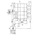
図1は本発明の一実施例による液晶表示装置のブロック図であり、図2は本発明の一実施例による液晶表示装置で1つの画素の等価回路図である。
図1に示すように、本発明の一実施例による液晶表示装置は液晶表示板組立体300及びこれと接続されたゲート駆動部400及びデータ駆動部500、データ駆動部500に接続された階調電圧生成部800、電荷供給部700そしてこれらを制御する信号制御部600を含む。
First, a liquid crystal display device according to an embodiment of the present invention will be described in detail with reference to FIGS.
FIG. 1 is a block diagram of a liquid crystal display device according to an embodiment of the present invention, and FIG. 2 is an equivalent circuit diagram of one pixel in the liquid crystal display device according to an embodiment of the present invention.
As shown in FIG. 1, a liquid crystal display according to an embodiment of the present invention includes a liquid
液晶表示板組立体300は、等価回路で見る時複数の信号線(G1−Gn、D1−Dm)とこれに接続されており、ほぼ行列形態で配列された複数の画素(PX)を含む。反面、図2に示した構造で見る時液晶表示板組立体300は互いに対向する下部及び上部表示板100、200とその間に注入された液晶層3を含む。
信号線(G1−Gn、D1−Dm)はゲート信号(“走査信号”とも言う)を伝達する複数のゲート線(G1−Gn)とデータ電圧を伝達する複数のデータ線(D1−Dm)を含む。ゲート線(G1−Gn)は互いにほぼ平行になるように行方向(図の左右方向)に延長され、データ線(D1−Dm)は互いにほぼ平行になるように列方向(図の上下方向)に延長される。
The liquid
The signal lines (G 1 -G n , D 1 -D m ) are a plurality of gate lines (G 1 -G n ) that transmit gate signals (also referred to as “scanning signals”) and a plurality of data lines that transmit data voltages. including (D 1 -D m). The gate lines (G 1 -G n ) are extended in the row direction (left-right direction in the drawing) so as to be substantially parallel to each other, and the data lines (D 1 -D m ) are arranged in the column direction (see FIG. In the vertical direction).
各画素(PX)、例えばi番目(i=1、2、…、n)ゲート線(Gi)とj番目(j=1、2、…、m)データ線(Dj)に接続された画素(PX)は信号線(Gi、Dj)に接続されたスイッチング素子(Q)とこれに接続された液晶キャパシタ(Clc)及びストレージキャパシタ(Cst)を含む。ストレージキャパシタ(Cst)は必要に応じて省略することができる。 Connected to each pixel (PX), for example, the i th (i = 1, 2,..., N) gate line (G i ) and the j th (j = 1, 2,..., M) data line (D j ). The pixel (PX) includes a switching element (Q) connected to the signal lines (G i , D j ), a liquid crystal capacitor (Clc), and a storage capacitor (Cst) connected thereto. The storage capacitor (Cst) can be omitted if necessary.
スイッチング素子(Q)は下部表示板100に設けられた薄膜トランジスタなどの三端子素子であって、その制御端子はゲート線(Gi)と接続されており、入力端子はデータ線(Dj)と接続されており、出力端子は液晶キャパシタ(Clc)及びストレージキャパシタ(Cst)と接続されている。薄膜トランジスタは多結晶シリコンや非晶質シリコンを含む構成とすることができる。
The switching element (Q) is a three-terminal element such as a thin film transistor provided on the
液晶キャパシタ(Clc)は、下部表示板100の画素電極191と上部表示板200の共通電極270とを2つの端子とし、この2つの電極191、270の間の液晶層3が両端子間の誘電体として機能することによって構成される。画素電極191はスイッチング素子(Q)と接続されており、共通電極270は上部表示板200の前面に形成されて共通電圧(Vcom)が印加される。図2の場合とは異なって、共通電極270を下部表示板100に設けることもでき、この時には2つの電極191、270のうちの少なくとも一方の電極が線状または棒状に形成することが望ましい。
The liquid crystal capacitor (Clc) has the
液晶キャパシタ(Clc)の補助的な役割を果たすストレージキャパシタ(Cst)は、下部表示板100に設けられた別個の信号線(図示せず)と画素電極191とが絶縁体を間に置いて重畳することによって形成され、この別個の信号線には共通電圧(Vcom)などの決められた電圧が印加される。このような場合とは異なり、画素電極191が絶縁体を媒介として真上の前段ゲート線と重畳することによってストレージキャパシタ(Cst)を構成することもできる。
In the storage capacitor Cst, which plays an auxiliary role for the liquid crystal capacitor Clc, a separate signal line (not shown) provided on the
一方、色表示を実現するためには、各画素(PX)が基本色のうちの1つを固有に表示する空間分割方式、各画素(PX)が時間によって交互に基本色を表示する時間分割方式などにより、これら基本色の空間的、時間的合計で所望の色相が認識されるようにする。基本色の例としては赤色、緑色、青色など三原色を挙げることができる。図2は空間分割の一例として、各画素(PX)が画素電極191に対応する上部表示板200の領域に基本色のうちの1つを示す色フィルター230が形成された場合を示している。図2とは異なって、色フィルター230を下部表示板100の画素電極191上または下に形成することもできる。
On the other hand, in order to realize color display, each pixel (PX) uniquely displays one of the basic colors in a spatial division method, and each pixel (PX) alternately displays a basic color according to time. A desired hue is recognized as a spatial and temporal sum of these basic colors by a method or the like. Examples of basic colors include three primary colors such as red, green, and blue. FIG. 2 shows a case where a
液晶表示板組立体300には少なくとも一偏光子(図示せず)が設けられている。
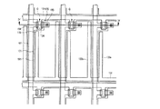
以下、このような液晶表示板組立体300の詳細構造について図3及び図4を参照して詳細に説明する。
図3は本発明の一実施例による液晶表示板組立体の配置図であり、図4は図3の液晶表示板組立体をIV−IV線に沿って切って示した断面図である。
The liquid
Hereinafter, the detailed structure of the liquid
FIG. 3 is a layout view of a liquid crystal panel assembly according to an embodiment of the present invention, and FIG. 4 is a cross-sectional view of the liquid crystal panel assembly of FIG. 3 cut along line IV-IV.
図3及び図4に示すように本発明の一実施例による液晶表示板組立体は前述したように、下部表示板100と上部表示板200及びその間に注入された液晶層3を含む。
まず、下部表示板100について説明する。
透明なガラスまたはプラスチックなどで構成された絶縁基板110上に複数のゲート線121及び複数の維持電極線131が形成されている。
3 and 4, the liquid crystal panel assembly according to an embodiment of the present invention includes a
First, the
A plurality of gate lines 121 and a plurality of
ゲート線121は、ゲート信号を伝達して主に図の横方向に延長されている。各ゲート線121は、下に突出した複数のゲート電極124と他の層または外部駆動回路との接続のために幅が拡大された端部(図示せず)を含む。ゲート信号を生成するゲート駆動回路(図示せず)は、基板110上に取り付けられる可撓性印刷回路膜(図示せず)上に装着することができ、基板110上に直接装着することもでき、また基板110に集積することも可能である。ゲート駆動回路を基板110上に集積する場合には、ゲート線121を延長してこれと直接接続することが可能である。
The gate line 121 transmits a gate signal and extends mainly in the horizontal direction in the figure. Each gate line 121 includes a plurality of
維持電極線131は所定の電圧が印加されるものであって、ゲート線121とほぼ平行に延長された幹線と、この幹線から分岐する複数対の維持電極(133a、133b)を含む。維持電極線131はそれぞれ隣接する2つのゲート線121の間に位置しており、幹線は2つのゲート線12のうちの下側に近い位置に形成される。維持電極(133a、133b)はそれぞれ幹線と接続された固定端とその反対側の自由端を有している。維持電極線131は、図示したものに限定されるものではなく、その形状及び配置は多様に変形することができる。
The
ゲート線121及び維持電極線131は、アルミニウム(Al)やアルミニウム合金などアルミニウム系金属、銀(Ag)や銀合金など銀系金属、銅(Cu)や銅合金など銅系金属、モリブデン(Mo)やモリブデン合金などモリブデン系金属、クロム(Cr)、タンタル(Ta)及びチタン(Ti)などで形成することができる。しかしながら、これらは物理的性質が他の2つの導電膜(図示せず)を含む多重膜構造を有することもできる。このうちの一方の導電膜は、信号遅延や電圧降下を軽減することができるように、比抵抗が低い金属、例えばアルミニウム系金属、銀系金属、銅系金属などで形成できる。また、他方の導電膜は異なる物質、特にITO(酸化インジウム錫)及びIZO(酸化インジウム亜鉛)との物理的、化学的、電気的接触特性に優れた物質、例えばモリブデン系金属、クロム、タンタル、チタンなどで形成することができる。このような組み合わせの良い例としては、クロム下部膜とアルミニウム(合金)上部膜及びアルミニウム(合金)下部膜とモリブデン(合金)上部膜を挙げることができる。しかしながら、ゲート線121及び維持電極線131は例示したものに限定されるものではなく、その他にも多様な金属または導電体で形成することができる。
The gate line 121 and the
ゲート線121及び維持電極線131の側面は基板110面に対して傾いており、その傾斜角は約30゜〜約80゜であることが好ましい。
ゲート線121及び維持電極線131上には窒化珪素(SiNx)または酸化珪素(SiOx)などで作られたゲート絶縁膜140が形成されている。
ゲート絶縁膜140上には、水素化非晶質シリコン(非晶質シリコンは略称a−Siとして使う)または多結晶シリコンなどで形成された複数の島型半導体154が形成されている。半導体154はゲート電極124上に位置する。
The side surfaces of the gate line 121 and the
A
On the
半導体154上には複数の島型抵抗性接触部材163、165が形成されている。抵抗性接触部材163、165は、燐などのn型不純物が高濃度でドーピングされているn+水素化非晶質珪素などの物質、またはシリサイドで形成することができる。抵抗性接触部材163、165は対を構成して半導体154上に配置されている。
半導体154と抵抗性接触部材163、165の側面は基板110面に対して傾いており、その傾斜角は30゜〜80゜程度とすることが好ましい。
A plurality of island-type
The side surfaces of the
抵抗性接触部材163、165及びゲート絶縁膜140上には複数のデータ線171と複数のドレーン電極175が形成されている。
データ線171は、データ信号を伝達して主に図の縦方向に延長されてゲート線121と交差する。各データ線171はまた、維持電極線131と交差して隣接した維持電極(133a、133b)集合の間に延長されている。各データ線171はまた、維持電極線131の幹線と交差する。各データ線171はゲート電極124に向かってのびた複数のソース電極173と、他の層または外部駆動回路との接続のために幅が拡大された端部(図示せず)を含む。データ信号を生成するデータ駆動回路(図示せず)は、基板110上に取り付けられた可撓性印刷回路膜(図示せず)上に装着することができ、基板110上に直接装着することもでき、また基板110に集積することも可能である。データ駆動回路を基板110上に集積する場合、データ線171を延長してこれと直接接続することができる。
A plurality of
The
ドレーン電極175はデータ線171と分離されており、ゲート電極124を中心にソース電極173と対向する。
1つのゲート電極124、1つのソース電極173及び1つのドレーン電極175は半導体154と一緒に1つの薄膜トランジスタ(TFT)(Q)を形成し、薄膜トランジスタ(Q)のチャンネルはソース電極173とドレーン電極175の間の半導体154に形成される。
The
One
データ線171及びドレーン電極175はモリブデン、クロム、タンタル及びチタンなど耐火性金属またはこれらの合金で形成されることが好ましく、耐火性金属膜(図示せず)と低抵抗導電膜(図示せず)を含む多重膜構造とすることができる。多重膜構造の例としては、クロムまたはモリブデン(合金)下部膜とアルミニウム(合金)上部膜の二重膜、モリブデン(合金)下部膜とアルミニウム(合金)中間膜とモリブデン(合金)上部膜の三重膜を挙げることができる。しかしながら、データ線171及びドレーン電極175は、例示したものに限定されるものではなく、その他にも多様な金属または導電体で形成することができる。
The
データ線171及びドレーン電極175また、その側面が基板110面に対して30゜〜80゜程度の傾斜角で傾いていることが好ましい。
抵抗性接触部材163、165は、その下の半導体154とその上のデータ線171及びドレーン電極175の間にだけ存在してこれらの間の接触抵抗を低くする。
データ線171、ドレーン電極175及び露出された半導体154部分上には保護膜180が形成されている。保護膜180は、無機絶縁物または有機絶縁物などで形成することができ、表面を平坦にすることが好ましい。無機絶縁物の例としては窒化シリコンと酸化シリコンを挙げることができる。有機絶縁物は、感光性を有する材料で構成することができ、その誘電定数は約4.0以下であることが好ましい。しかしながら、保護膜180は、有機膜の優れた絶縁特性を生かしながらも、露出した半導体154部分を損傷しないように下部無機膜と上部有機膜の二重膜構造とすることができる。
The
The
A
保護膜180には、データ線171の端部(図示せず)を各々露出する複数の接触孔(図示せず)とドレーン電極175を各々露出する複数の接触孔185が形成されており、保護膜180とゲート絶縁膜140にはゲート線121の端部(図示せず)を露出する複数の接触孔(図示せず)が形成されている。
保護膜180上には、複数の画素電極191及び複数の接触補助部材(図示せず)が形成されている。これらはITOまたはIZOなどの透明な導電物質やアルミニウム、銀、クロムまたはその合金などの反射性金属で形成することができる。
The
A plurality of
画素電極191は、接触孔185を通じてドレーン電極175と物理的・電気的に接続されており、ドレーン電極175からデータ信号が印加される。データ信号が印加された画素電極191は、共通電圧が印加される他の表示板200の共通電極270と一緒に電場を生成することによって、2つの電極191、270の間の液晶層3の液晶分子31の方向を決定する。このように決定された液晶分子31の方向によって、液晶層3を通過する光の偏光が変わる。画素電極191と共通電極270は液晶キャパシタを構成して薄膜トランジスタが遮断した後にも印加された電圧を維持する。
The
画素電極191は、維持電極(133a、133b)を始めとした維持電極線131と重畳する。画素電極191及びこれと電気的に接続されたドレーン電極175が維持電極線131と重畳して、液晶キャパシタの電圧維持能力を強化するストレージキャパシタを構成する。
接触補助部材(図示せず)は、各々接触孔(図示せず)を通じてゲート線121の端部(図示せず)及びデータ線171の端部(図示せず)と接続される。接触補助部材(図示せず)は、ゲート線121の端部(図示せず)及びデータ線171の端部(図示せず)と外部装置との接着性を補完してこれらを保護する。
The
The contact assistants (not shown) are connected to the end portions (not shown) of the gate lines 121 and the end portions (not shown) of the
次に、上部表示板200について説明する。
透明なガラスまたはプラスチックなどで構成された絶縁基板210上にブラックマトリックス220が形成されている。ブラックマトリックス220は、データ線171に対応する線状部分(図示せず)と薄膜トランジスタに対応する面型部分(図示せず)を含み、画素電極191の間の光漏れを防ぐ。
Next, the
A
基板210上にはまた、複数の色フィルター230が形成されている。色フィルター230は、そのほとんどの部分がブラックマトリックス220に囲まれた領域内に存在し、画素電極191列に沿って縦方向に長く延長された構成とすることができる。各色フィルター230は赤色、緑色及び青色の三原色など基本色のうちの1つを表示するように構成できる。
A plurality of
色フィルター230及びブラックマトリックス220上にはオーバーコートを形成することができる。オーバーコートは有機絶縁物で形成することができ、色フィルター230が露出することを防止し平坦面を提供することができる。このオーバーコートは省略することができる。
色フィルター230とブラックマトリックス220上には、共通電極270が形成されている。共通電極270はITO、IZOなどの透明な導電体などで形成することができる。
An overcoat can be formed on the
A
表示板100、200の内側面には同一の方向にラビングされている水平配向膜11、21が塗布されている。
表示板100、200の外側側面には、偏光子12、22が設けられているが、2個の偏光子12、22の透過軸は直交しており、このうちの1つの透過軸はゲート線121に対して平行であることが好ましい。反射型液晶表示装置の場合には2個の偏光子12、22のうちの1個を省略することができる。
Polarizers 12 and 22 are provided on the outer side surfaces of the
偏光子12、22と表示板100、200の間には補償フィルム13、23が設けられており、この補償フィルム13、23としてはCプレート補償フィルムまたは二軸性補償フィルムなどを使用することができる。
液晶層3は、誘電率異方性が正のネマチック液晶を含み、初期においてスプレイ配向されており、ベンド電圧によって図4のようにベンド配向に転換され、この状態で表示のための駆動が行われる。一般に、OCB液晶表示装置はノーマリーホワイト、つまり、電圧を印加しない状態でホワイトを表示する。
The
図1に示すように、階調電圧生成部800は、画素(PX)の透過率と関連した全体階調電圧または限定された個数の階調電圧(以下、“基準階調電圧”という)を生成する。(基準)階調電圧は共通電圧(Vcom)に対して正の値を有するものと負の値を有するものを含むことができる。
ゲート駆動部400は、液晶表示板組立体300のゲート線(G1−Gn)と接続されてゲートオン電圧(Von)とゲートオフ電圧(Voff)の組み合わせから成るゲート信号をゲート線(G1−Gn)に印加する。
As shown in FIG. 1, the
The
データ駆動部500は、液晶表示板組立体300のデータ線(D1−Dm)と接続されており、階調電圧生成部800からの階調電圧を選択してこれをデータ電圧としてデータ線(D1−Dm)に印加する。これに対し、階調電圧生成部800が階調電圧を全て提供せずに、限定された個数の基準階調電圧だけを提供する場合、データ駆動部500が基準階調電圧を分圧して所望のデータ電圧を生成するように構成できる。
The
電荷供給部700は、下部表示板100の周縁領域に位置する複数の電荷供給回路710を含む。このような電荷供給部700は下部表示板100の接続点(図示せず)を通じて上部表示板200の共通電極270に共通電圧またはベンド電圧を印加する。
それぞれの電荷供給回路710については詳細に後述する。
信号制御部600はゲート駆動部400、データ駆動部500及び電荷供給部700などを制御する。
The
Each
The
このような駆動装置400、500、600、700、800は、それぞれ少なくとも1つの集積回路チップの形態で液晶表示板組立体300上に直接装着することができ、可撓性印刷回路膜(図示せず)上に装着されてTCP(Tape Carrier Package)の形態で液晶表示板組立体300に取り付けることもでき、別途の印刷回路基板(図示せず)上に装着することもできる。これとは異なって、これら駆動装置400、500、600、700、800が信号線(G1−Gn、D1−Dm)及び薄膜トランジスタスイッチング素子(Q)などと一緒に液晶表示板組立体300に集積することも可能である。また、駆動装置400、500、600、700、800は全てを単一チップに集積することができ、また、これらのうちの少なくとも1つまたは複数を前述した単一チップの外側に配置した回路構成とするもでき、各装置を構成する回路素子のうちの1または複数を前述の単一チップの外側に配置した回路構成とすることもできる。
Each of the driving
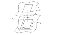
以下、図5及び図6を参照して電荷供給部700を用いた液晶層3の配向転移を調べる。
図5はベンド電圧を印加する前の液晶の配向状態を示した図面であり、図6はベンド電圧を印加した後の液晶の配向状態を示した図面である。
図5に示すように、ベンド電圧を印加しない状態で、2つの配向膜11、21近傍の液晶分子31はラビング方向に向かって一端が立ち上がった形態の先傾斜角を有して水平配向されている。従って、液晶分子31の配列は基板110、210面と平行で2つの配向膜11、21の表面からほぼ同じ距離にある面(以下、“中心面”という)を中心に対称を構成するようになる。このような配向をスプレイ配向という。
Hereinafter, the alignment transition of the
FIG. 5 is a drawing showing the alignment state of the liquid crystal before applying the bend voltage, and FIG. 6 is a drawing showing the alignment state of the liquid crystal after applying the bend voltage.
As shown in FIG. 5, without applying a bend voltage, the
このような状態で液晶層3に電場が印加されれば液晶分子31がスプレイ配向から他の配向に変化することとなる。
2つ表示板100、200の電極(図示せず)に電圧を印加し始めて、2つ表示板100、200の面に垂直である電場が液晶層3に生じれば、配向膜11、21近傍の液晶分子31が電場に反応して立ち上がる。ところが2つの配向膜11、21表面で液晶分子31の立ち上がる方向が同一なので、液晶層3の中間部分では液晶分子31の立ち上がる方向が衝突を起こし大きいストレスが生じ、これによりエネルギー的に安定なねじれ配向に転移される。これを転移スプレイ配向という。
If an electric field is applied to the
If a voltage is applied to the electrodes (not shown) of the two
この状態で電場を更に強くすれば、図6に示すように、液晶はベンド配向をするようになる。このような配向転移は、液晶表示板組立体300全体の液晶キャパシタ(Clc)で均一に発生する必要がある。
次に、図7及び図8を参照して本発明の一実施例による電荷供給回路の構造について説明する。
If the electric field is further strengthened in this state, the liquid crystal will bend as shown in FIG. Such alignment transition needs to occur uniformly in the liquid crystal capacitor (Clc) of the entire liquid
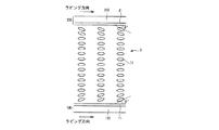
Next, the structure of a charge supply circuit according to an embodiment of the present invention will be described with reference to FIGS.
図7は本発明の一実施例による電荷供給回路を示した回路図であり、図8は本発明の一実施例による液晶表示装置の動作を示す信号波形図である。
図7に示すように、それぞれの電荷供給回路710はキャパシタ(Cb)及び複数のスイッチング素子(S1、S2、S3)を含む。
スイッチング素子(S1)は三端子素子であって、第1制御信号(G1)と接続されている制御端子、共通電圧(Vcom)と接続されている入力端子及び出力端(OUT)と接続されている出力端子を含む。
FIG. 7 is a circuit diagram showing a charge supply circuit according to one embodiment of the present invention, and FIG. 8 is a signal waveform diagram showing the operation of the liquid crystal display device according to one embodiment of the present invention.
As shown in FIG. 7, each
The switching element (S1) is a three-terminal element, and is connected to the control terminal connected to the first control signal (G1), the input terminal connected to the common voltage (Vcom), and the output terminal (OUT). Including output terminals.
スイッチング素子(S2)はまた、三端子素子であって、第2制御信号(G2)と接続されている制御端子、ベンド電圧(Vbend)と接続されている入力端子及び節点(n1)と接続されている出力端子を含む。
スイッチング素子(S3)はまた、三端子素子であって、第3制御信号(G3)と接続されている制御端子、節点(n1)と接続されている入力端子及び出力端(OUT)と接続されている出力端子を含む。
The switching element (S2) is also a three-terminal element, and is connected to the control terminal connected to the second control signal (G2), the input terminal connected to the bend voltage (Vbend), and the node (n1). Output terminal.
The switching element (S3) is also a three-terminal element, and is connected to the control terminal connected to the third control signal (G3), the input terminal connected to the node (n1), and the output terminal (OUT). Output terminal.
キャパシタ(Cb)は共通電圧(Vcom)と節点(n1)の間に接続されている。
複数の電荷供給回路710の出力端(OUT)は下部表示板100の接続点を通じて上部表示板200の共通電極270と接続されている。
次に、このような液晶表示装置の動作について詳細に説明する。
外部から(図示せず)信号が印加されれば、信号制御部600は配向制御信号(CONT3)を電荷供給部700に出力する。
The capacitor (Cb) is connected between the common voltage (Vcom) and the node (n1).
Output terminals (OUT) of the plurality of
Next, the operation of such a liquid crystal display device will be described in detail.
When a signal is applied from the outside (not shown), the
このような配向制御信号(CONT3)は第1〜第3制御信号(G1、G2、G3)を含む。
まず、ハイレベルの第2制御信号(G2)が印加されれば、各電荷供給回路710のスイッチング素子(S2)が導通して節点(n1)にベンド電圧(Vbend)を伝達する。ベンド電圧(Vbend)は直流電圧として共通電圧(Vcom)より高いレベルを有する。
Such an orientation control signal (CONT3) includes first to third control signals (G1, G2, G3).
First, when a high-level second control signal (G2) is applied, the switching element (S2) of each
キャパシタ(Cb)は共通電圧(Vcom)とベンド電圧(Vbend)の差電圧に相応する電荷を充電する。
次に、ハイレベルの第3制御信号(G3)が印加され、第2制御信号(G2)がローレベルに遷移すれば、スイッチング素子(S2)が遮断してスイッチング素子(S3)が導通する。
The capacitor (Cb) is charged with a charge corresponding to the difference voltage between the common voltage (Vcom) and the bend voltage (Vbend).
Next, when the high-level third control signal (G3) is applied and the second control signal (G2) transitions to the low level, the switching element (S2) is cut off and the switching element (S3) is turned on.
これにより、キャパシタ(Cb)と液晶キャパシタ(Clc)の間の電圧差によってキャパシタ(Cb)から液晶キャパシタ(Clc)側に電流が流れてキャパシタ(Cb)に充電されていた電荷が出力端(OUT)を通じて共通電極270に接続された液晶キャパシタ(Clc)に充電される。
このようなスイッチング素子(S2、S3)の動作が複数回にかけて繰り返されれば液晶キャパシタ(Clc)には多くの電荷が充電されて共通電極270全体が均一にベンド電圧(Vbend)のようなレベルの電圧を有する。従って、液晶層3はベンド電圧(Vbend)に相応する電場によってベンド配向に転移する。
Thereby, a current flows from the capacitor (Cb) to the liquid crystal capacitor (Clc) side due to a voltage difference between the capacitor (Cb) and the liquid crystal capacitor (Clc), and the charge charged in the capacitor (Cb) is output to the output terminal (OUT ) To charge the liquid crystal capacitor (Clc) connected to the
If the operation of the switching elements (S2, S3) is repeated a plurality of times, the liquid crystal capacitor (Clc) is charged with a large amount of charge, and the entire
この時、現在共通電極270の電圧であるVcomrealがベンド電圧(Vbend)と近くなることによって(Cb、Clc)両キャパシタの電流ピークは次第に低くなって、これによりキャパシタ(Cb)で液晶キャパシタ(Clc)に伝達される電荷量が減る。従って、スイッチング素子(S2、S3)のオン/オフが繰り返されるによってベンド電圧(Vbend)のレベルを上昇させることによって(Cb、Clc)両キャパシタの間の移動電荷量を増やすことができて、短時間のうちに液晶キャパシタ(Clc)を均一に充電することができる。
At this time, the current peak of the
一方、スイッチング素子(S2、S3)が導通/遮断を繰り返す間スイッチング素子(S1)は遮断状態を維持する。
液晶層3が配向転移を終えれば、第1及び第2制御信号(G1、G2)がローレベルに遷移して、第3制御信号(G3)がハイレベルに遷移する。
従って、スイッチング素子(S2、S3)が遮断して、スイッチング素子(S1)が導通して出力端(OUT)を通じて共通電極270に共通電圧Vcomが印加される。
On the other hand, while the switching elements (S2, S3) are repeatedly turned on / off, the switching element (S1) maintains the cutoff state.
When the
Accordingly, the switching elements (S2, S3) are cut off, the switching element (S1) is turned on, and the common voltage Vcom is applied to the
共通電極270に共通電圧(Vcom)が印加された状態で、信号制御部600は外部のグラフィック制御器(図示せず)から入力映像信号(R、G、B)及びその表示を制御する入力制御信号を受信する。入力映像信号(R、G、B)は各画素(PX)の輝度情報を載せており、輝度は決められた個数、例えば1024(=210)、256(=28)または64(=26)個の階調を有している。入力制御信号の例としては垂直同期信号(Vsync)と水平同期信号(Hsync)、メインクロック(MCLK)、データイネーブル信号(DE)などがある。
In a state in which a common voltage (Vcom) is applied to the
信号制御部600は入力映像信号(R、G、B)と入力制御信号に基づいて入力映像信号(R、G、B)を液晶表示板組立体300の動作条件に合うように適切に処理してゲート制御信号(CONT1)及びデータ制御信号(CONT2)などを生成した後、ゲート制御信号(CONT1)をゲート駆動部400に送出して、データ制御信号(CONT2)と処理した映像信号(DAT)をデータ駆動部500に送出する。
The
ゲート制御信号(CONT1)は走査開始を指示する走査開始信号(STV)とゲートオン電圧(Von)の出力周期を制御する少なくとも1つのクロック信号を含む。ゲート制御信号(CONT1)はまた、ゲートオン電圧(Von)の持続時間を限定する出力イネーブル信号(OE)を更に含むように構成できる。
データ制御信号(CONT2)は1つの行の画素(PX)に対するデジタル映像信号(DAT)の伝送開始を知らせる水平同期開始信号(STH)と、データ線(D1−Dm)にアナログデータ電圧を印加するロード信号(LOAD)及びデータクロック信号(HCLK)を含む。データ制御信号(CONT2)は、共通電圧(Vcom)に対するアナログデータ電圧の電圧極性(以下、“共通電圧に対するデータ電圧の極性”を縮めて“データ電圧の極性”という)を反転させる反転信号(RVS)を更に含む構成とすることができる。
The gate control signal (CONT1) includes a scanning start signal (STV) for instructing the start of scanning and at least one clock signal for controlling the output cycle of the gate-on voltage (Von). The gate control signal (CONT1) can also be configured to further include an output enable signal (OE) that limits the duration of the gate-on voltage (Von).
A data control signal (CONT2) is a horizontal synchronization start signal for informing the start of transmission of a digital video signal (DAT) for the pixels (PX) of one row (STH), the analog data voltages to the data lines (D 1 -D m) It includes a load signal (LOAD) and a data clock signal (HCLK) to be applied. The data control signal (CONT2) is an inversion signal (RVS) that inverts the voltage polarity of the analog data voltage with respect to the common voltage (Vcom) (hereinafter referred to as “the polarity of the data voltage relative to the common voltage”). ).
信号制御部600からのデータ制御信号(CONT2)によって、データ駆動部500は1つの行の画素(PX)に対するデジタル映像信号(DAT)を受信して、各デジタル映像信号(DAT)に対応する階調電圧を選択することによってデジタル映像信号(DAT)をアナログデータ電圧に変換した後、これを当該データ線(D1−Dm)に印加する。
In response to the data control signal (CONT2) from the
ゲート駆動部400は、信号制御部600からのゲート制御信号(CONT1)によってゲートオン電圧(Von)をゲート線(G1−Gn)に印加してこのゲート線(G1−Gn)に接続されたスイッチング素子(Q)を導通させる。そうすれば、データ線(D1−Dm)に印加されたデータ電圧が導通したスイッチング素子(Q)を通じて当該画素(PX)に印加される。
The
画素(PX)に印加されたデータ電圧と共通電圧(Vcom)との差は、液晶キャパシタ(Clc)の充電電圧、つまり、画素電圧として示される。液晶分子は画素電圧の大きさによってその配列を別にして、これにより液晶層3を通過する光の偏光が変化する。このような偏光の変化は液晶表示板組立体300に取り付けられた偏光子によって光の透過率変化に示され、これによって画素(PX)は映像信号(DAT)の階調を示す輝度を表示する。
The difference between the data voltage applied to the pixel (PX) and the common voltage (Vcom) is shown as the charging voltage of the liquid crystal capacitor (Clc), that is, the pixel voltage. The liquid crystal molecules are arranged differently depending on the magnitude of the pixel voltage, whereby the polarization of light passing through the
1水平周期(“1H”とも称し、水平同期信号(Hsync)及びデータイネーブル信号(DE)の一周期と同一である)を単位にしてこのような過程を繰り返すことによって、全てのゲート線(G1−Gn)に対して順にゲートオン電圧(Von)を印加して全ての画素(PX)にデータ電圧を印加して1フレームの映像を表示する。
1フレームが終われば、次フレームが始まって各画素(PX)に印加されるデータ電圧の極性が直前フレームでの極性と反対になるようにデータ駆動部500に印加される反転信号(RVS)の状態が制御される(“フレーム反転”)。この時、1フレーム内でも反転信号(RVS)の特性によって1つのデータ線を通じて流れるデータ電圧の極性が変更するように構成でき(例:行反転、点反転)、1つの画素の行に印加されるデータ電圧の極性を互いに異なるようにすることもできる(例:列反転、点反転)。
By repeating such a process in units of one horizontal cycle (also referred to as “1H”, which is the same as one cycle of the horizontal sync signal (Hsync) and the data enable signal (DE)), all the gate lines (G A gate-on voltage (Von) is sequentially applied to 1 -G n ), and a data voltage is applied to all the pixels (PX) to display one frame of video.
When one frame ends, the next frame starts and the inverted signal (RVS) applied to the
以上、本発明の好ましい実施例について説明したが、本発明の権利範囲はこれに限定されるものではなく、特許請求の範囲と発明の詳細な説明及び添付した図面の範囲内で多様に変形して実施するのが可能であり、これもまた本発明の範囲に属することは当然である。 The preferred embodiment of the present invention has been described above, but the scope of the present invention is not limited to this, and various modifications may be made within the scope of the claims, the detailed description of the invention and the attached drawings. Naturally, this also falls within the scope of the present invention.
3 液晶層
11、21 配向膜
31 液晶分子
100、200 表示板
110、210 基板
300 液晶表示板組立体
700 電荷供給部
Clc 液晶キャパシタ
3 Liquid crystal layers 11 and 21
Claims (7)
前記第1基板上に形成された第1電極と、
前記第1基板と対向する第2基板と、
前記第2基板上に形成されており、前記第1電極と対向する第2電極と、
前記第1及び第2電極の間に液晶を注入することにより形成される液晶層と、
前記第1電極に複数回にかけて電荷を供給することによって前記液晶の配向をスプレイ配向からベンド配向に転移させるベンド電圧を印加する複数の電荷供給部と、
を含み、
前記電荷供給部は、前記液晶表示装置が映像を表示する前に前記ベンド電圧を前記第1電極に印加し、前記液晶表示装置が映像を表示する間に前記第1電極に共通電圧を印加する、液晶表示装置。 A first substrate;
A first electrode formed on the first substrate;
A second substrate facing the first substrate;
A second electrode formed on the second substrate and facing the first electrode;
A liquid crystal layer formed by injecting liquid crystal between the first and second electrodes;
A plurality of charge supply units for applying a bend voltage for transferring the alignment of the liquid crystal from a splay alignment to a bend alignment by supplying a charge to the first electrode a plurality of times;
Only including,
The charge supply unit applies the bend voltage to the first electrode before the liquid crystal display device displays an image, and applies a common voltage to the first electrode while the liquid crystal display device displays an image. , a liquid crystal display device.
前記共通電圧と基準節点の間に接続されたキャパシタと、
ベンド電圧と前記基準節点の間に接続された第1スイッチング素子と、
前記基準節点と前記第1電極の間に接続された第2スイッチング素子と、
を含む、請求項1に記載の液晶表示装置。 The charge supply unit includes:
A capacitor connected between the common voltage and a reference node;
A first switching element connected between a bend voltage and the reference node;
A second switching element connected between the reference node and the first electrode;
The liquid crystal display device according to claim 1 , comprising:
前記第3スイッチング素子は、前記第1電極が前記ベンド電圧で充電された後導通する、請求項4に記載の液晶表示装置。 The charge supply unit further includes a third switching element connected between the common voltage and the first electrode,
The liquid crystal display device according to claim 4 , wherein the third switching element is turned on after the first electrode is charged with the bend voltage.
前記液晶表示装置が映像を表示する前に前記電荷供給部により、第1電極に複数回にかけて前記ベンド電圧を供給することによって前記液晶の配向をスプレイ配向からベンド配向に転移させるベンド電圧を印加する段階と、
前記液晶表示装置が映像を表示する間に前記電荷供給部により、第1電極に共通電圧を印加する段階と、
前記液晶表示装置が映像を表示する間に第2電極にデータ電圧を印加して映像を表示する段階と、
を含む、液晶表示装置の駆動方法。 A first substrate, a first electrode formed on the first substrate, a second substrate facing the first substrate, a second electrode formed on the second substrate and facing the first electrode, to transition from splay alignment to bend alignment orientation of the liquid crystal by supplying a charge over the multiple liquid crystal layers are formed, and on the first electrode by injecting a liquid crystal between the first and second electrodes In a driving method of a liquid crystal display device including a plurality of charge supply units for applying a bend voltage ,
Before the liquid crystal display device displays an image, the charge supply unit applies a bend voltage for changing the alignment of the liquid crystal from a splay alignment to a bend alignment by supplying the bend voltage to the first electrode a plurality of times. Stages,
Applying a common voltage to the first electrode by the charge supply unit while the liquid crystal display device displays an image ;
Applying a data voltage to the second electrode while the liquid crystal display device displays an image to display the image;
A method for driving a liquid crystal display device, comprising:
Applications Claiming Priority (2)
| Application Number | Priority Date | Filing Date | Title |
|---|---|---|---|
| KR1020060094245A KR101272333B1 (en) | 2006-09-27 | 2006-09-27 | LIQUID CRYSTAL DISPLAY and DRIVING MATHOD THEREOF |
| KR10-2006-0094245 | 2006-09-27 |
Publications (3)
| Publication Number | Publication Date |
|---|---|
| JP2008083706A JP2008083706A (en) | 2008-04-10 |
| JP2008083706A5 JP2008083706A5 (en) | 2010-10-21 |
| JP5250737B2 true JP5250737B2 (en) | 2013-07-31 |
Family
ID=39032227
Family Applications (1)
| Application Number | Title | Priority Date | Filing Date |
|---|---|---|---|
| JP2007251317A Expired - Fee Related JP5250737B2 (en) | 2006-09-27 | 2007-09-27 | Liquid crystal display device and driving method thereof |
Country Status (5)
| Country | Link |
|---|---|
| US (1) | US7903065B2 (en) |
| EP (1) | EP1909256B1 (en) |
| JP (1) | JP5250737B2 (en) |
| KR (1) | KR101272333B1 (en) |
| CN (1) | CN101153974B (en) |
Cited By (1)
| Publication number | Priority date | Publication date | Assignee | Title |
|---|---|---|---|---|
| JP2662702B2 (en) | 1988-10-05 | 1997-10-15 | 住友電気工業株式会社 | Manufacturing method of foam metal |
Families Citing this family (3)
| Publication number | Priority date | Publication date | Assignee | Title |
|---|---|---|---|---|
| CN108828842B (en) * | 2013-02-27 | 2021-07-27 | 视瑞尔技术公司 | Phase modulator |
| CN104298040B (en) * | 2014-10-31 | 2018-07-06 | 京东方科技集团股份有限公司 | A kind of COA substrates and preparation method thereof and display device |
| CN114326193B (en) * | 2021-12-30 | 2024-01-26 | 惠科股份有限公司 | Flexible color film substrate, display panel, display device and electronic equipment |
Family Cites Families (33)
| Publication number | Priority date | Publication date | Assignee | Title |
|---|---|---|---|---|
| JPH10206822A (en) * | 1997-01-20 | 1998-08-07 | Internatl Business Mach Corp <Ibm> | Voltage application driving system |
| JP3161393B2 (en) * | 1997-11-28 | 2001-04-25 | 日本電気株式会社 | Active matrix type liquid crystal display |
| US6809717B2 (en) * | 1998-06-24 | 2004-10-26 | Canon Kabushiki Kaisha | Display apparatus, liquid crystal display apparatus and driving method for display apparatus |
| EP1235101A3 (en) | 1998-09-03 | 2008-08-20 | Toshiba Matsushita Display Technology Co., Ltd. | Liquid crystal display device, method for manufacturing the same, and method for driving a liquid crystal display device |
| TW442978B (en) * | 1998-10-16 | 2001-06-23 | Seiko Epson Corp | Driver circuit of electro-optical device and driving method, D/A converter, signal driver, electro-optical panel, projection display, and electronic machine |
| US6642984B1 (en) * | 1998-12-08 | 2003-11-04 | Fujitsu Display Technologies Corporation | Liquid crystal display apparatus having wide transparent electrode and stripe electrodes |
| JP2000321556A (en) * | 1999-05-14 | 2000-11-24 | Sanyo Electric Co Ltd | Method for transition of alignment state of liquid crystal and method of driving liquid crystal display device |
| JP4891529B2 (en) | 1999-10-19 | 2012-03-07 | 東芝モバイルディスプレイ株式会社 | Liquid crystal device |
| EP1113412B1 (en) | 1999-12-27 | 2014-05-21 | Japan Display Inc. | Liquid crystal display apparatus and method for driving the same |
| JP4615174B2 (en) * | 2000-01-21 | 2011-01-19 | シチズンホールディングス株式会社 | Liquid crystal display device |
| JP2002094955A (en) * | 2000-02-22 | 2002-03-29 | Philips Japan Ltd | Image display and pickup device |
| TW513598B (en) * | 2000-03-29 | 2002-12-11 | Sharp Kk | Liquid crystal display device |
| US6475792B1 (en) * | 2000-10-12 | 2002-11-05 | Marical, Llc | Methods for raising pre-adult anadromous fish |
| EP1331507A4 (en) * | 2000-10-25 | 2008-04-16 | Toshiba Matsushita Display Tec | Liquid crystal display drive method and liquid crystal display |
| JP4895450B2 (en) * | 2000-11-10 | 2012-03-14 | 三星電子株式会社 | Liquid crystal display device and driving device and method thereof |
| KR100783704B1 (en) | 2001-04-26 | 2007-12-07 | 삼성전자주식회사 | Liquid Crystal Display and driving apparatus and method thereof |
| JP4189122B2 (en) * | 2000-12-04 | 2008-12-03 | 東芝松下ディスプレイテクノロジー株式会社 | Liquid crystal display device and image display application device |
| JP4138272B2 (en) * | 2001-06-04 | 2008-08-27 | 東芝松下ディスプレイテクノロジー株式会社 | Method for driving liquid crystal display device and liquid crystal display device using the same |
| JP3655217B2 (en) * | 2001-06-21 | 2005-06-02 | 株式会社東芝 | Driving method of liquid crystal display element |
| JP2002278524A (en) * | 2001-12-14 | 2002-09-27 | Matsushita Electric Ind Co Ltd | Liquid crystal display device, liquid crystal module and method of driving liquid crystal display device |
| KR100843685B1 (en) | 2001-12-27 | 2008-07-04 | 엘지디스플레이 주식회사 | Method and apparatus for driving a liquid crystal display |
| JP3888921B2 (en) * | 2002-03-28 | 2007-03-07 | 株式会社アドバンスト・ディスプレイ | Liquid crystal display element |
| KR100864972B1 (en) | 2002-06-25 | 2008-10-23 | 엘지디스플레이 주식회사 | Reset driving device of LCD and reset method |
| KR100870516B1 (en) | 2002-07-26 | 2008-11-26 | 엘지디스플레이 주식회사 | LCD and its driving method |
| KR100951358B1 (en) | 2003-09-05 | 2010-04-08 | 삼성전자주식회사 | Liquid crystal display and its driving device |
| JP2005156717A (en) * | 2003-11-21 | 2005-06-16 | Sony Corp | Liquid crystal display element and liquid crystal display device |
| KR100808315B1 (en) | 2004-02-20 | 2008-02-27 | 도시바 마쯔시따 디스플레이 테크놀로지 컴퍼니, 리미티드 | Liquid crystal display device |
| KR100623713B1 (en) * | 2004-12-10 | 2006-09-19 | 삼성에스디아이 주식회사 | LCD and its driving method |
| KR100700645B1 (en) * | 2005-01-10 | 2007-03-27 | 삼성에스디아이 주식회사 | LCD and its driving method |
| KR100700647B1 (en) * | 2005-01-24 | 2007-03-27 | 삼성에스디아이 주식회사 | Liquid crystal display |
| US7999900B2 (en) * | 2005-09-15 | 2011-08-16 | Hiap L. Ong and Kyoritsu Optronics Co., Ltd | Display unit with interleaved pixels |
| JP2007114278A (en) * | 2005-10-18 | 2007-05-10 | Fuji Xerox Co Ltd | Driving method of optical address type spatial optical modulator and driving device of optical address type spatial optical modulator |
| TWI356228B (en) * | 2006-12-11 | 2012-01-11 | Chimei Innolux Corp | Liquid crystal display device |
-
2006
- 2006-09-27 KR KR1020060094245A patent/KR101272333B1/en not_active Expired - Fee Related
-
2007
- 2007-09-20 EP EP07018455.1A patent/EP1909256B1/en not_active Not-in-force
- 2007-09-26 US US11/861,963 patent/US7903065B2/en not_active Expired - Fee Related
- 2007-09-26 CN CN2007101619343A patent/CN101153974B/en not_active Expired - Fee Related
- 2007-09-27 JP JP2007251317A patent/JP5250737B2/en not_active Expired - Fee Related
Cited By (1)
| Publication number | Priority date | Publication date | Assignee | Title |
|---|---|---|---|---|
| JP2662702B2 (en) | 1988-10-05 | 1997-10-15 | 住友電気工業株式会社 | Manufacturing method of foam metal |
Also Published As
| Publication number | Publication date |
|---|---|
| EP1909256A2 (en) | 2008-04-09 |
| US7903065B2 (en) | 2011-03-08 |
| EP1909256B1 (en) | 2015-02-25 |
| US20080074569A1 (en) | 2008-03-27 |
| CN101153974B (en) | 2011-05-04 |
| JP2008083706A (en) | 2008-04-10 |
| CN101153974A (en) | 2008-04-02 |
| EP1909256A3 (en) | 2010-01-27 |
| KR20080028664A (en) | 2008-04-01 |
| KR101272333B1 (en) | 2013-06-10 |
Similar Documents
| Publication | Publication Date | Title |
|---|---|---|
| JP5078483B2 (en) | Liquid crystal display | |
| CN1959480B (en) | Liquid crystal display | |
| JP5111808B2 (en) | Thin film transistor display panel | |
| JP2008033324A (en) | Liquid crystal display | |
| JP5470609B2 (en) | Display device | |
| JP5229858B2 (en) | Liquid crystal display | |
| JP2005309437A (en) | Display device and driving method thereof | |
| CN1945413B (en) | Liquid crystal display | |
| CN1932594B (en) | Liquid crystal display and driving method thereof | |
| JP2007316635A (en) | Liquid crystal display | |
| US8711302B2 (en) | Liquid crystal display | |
| CN101114095B (en) | Liquid crystal display and driving method thereof | |
| JP5250737B2 (en) | Liquid crystal display device and driving method thereof | |
| JP2007164175A (en) | Display device | |
| KR20070060660A (en) | Liquid crystal display | |
| KR20070117046A (en) | Liquid crystal display | |
| KR20080022876A (en) | Liquid Crystal Display and Thin Film Transistor Display Panel | |
| KR20070083006A (en) | Liquid crystal display |
Legal Events
| Date | Code | Title | Description |
|---|---|---|---|
| A521 | Request for written amendment filed |
Free format text: JAPANESE INTERMEDIATE CODE: A523 Effective date: 20100907 |
|
| A621 | Written request for application examination |
Free format text: JAPANESE INTERMEDIATE CODE: A621 Effective date: 20100907 |
|
| A521 | Request for written amendment filed |
Free format text: JAPANESE INTERMEDIATE CODE: A523 Effective date: 20110805 |
|
| A977 | Report on retrieval |
Free format text: JAPANESE INTERMEDIATE CODE: A971007 Effective date: 20120718 |
|
| A131 | Notification of reasons for refusal |
Free format text: JAPANESE INTERMEDIATE CODE: A131 Effective date: 20120724 |
|
| A521 | Request for written amendment filed |
Free format text: JAPANESE INTERMEDIATE CODE: A523 Effective date: 20121002 |
|
| RD02 | Notification of acceptance of power of attorney |
Free format text: JAPANESE INTERMEDIATE CODE: A7422 Effective date: 20121002 |
|
| A711 | Notification of change in applicant |
Free format text: JAPANESE INTERMEDIATE CODE: A712 Effective date: 20121213 |
|
| A01 | Written decision to grant a patent or to grant a registration (utility model) |
Free format text: JAPANESE INTERMEDIATE CODE: A01 Effective date: 20121218 |
|
| A61 | First payment of annual fees (during grant procedure) |
Free format text: JAPANESE INTERMEDIATE CODE: A61 Effective date: 20130107 |
|
| A521 | Request for written amendment filed |
Free format text: JAPANESE INTERMEDIATE CODE: A523 Effective date: 20130325 |
|
| R150 | Certificate of patent or registration of utility model |
Free format text: JAPANESE INTERMEDIATE CODE: R150 |
|
| FPAY | Renewal fee payment (event date is renewal date of database) |
Free format text: PAYMENT UNTIL: 20160426 Year of fee payment: 3 |
|
| LAPS | Cancellation because of no payment of annual fees |