JP5249342B2 - Circuit apparatus and method for operating a high pressure discharge lamp - Google Patents
Circuit apparatus and method for operating a high pressure discharge lamp Download PDFInfo
- Publication number
- JP5249342B2 JP5249342B2 JP2010533441A JP2010533441A JP5249342B2 JP 5249342 B2 JP5249342 B2 JP 5249342B2 JP 2010533441 A JP2010533441 A JP 2010533441A JP 2010533441 A JP2010533441 A JP 2010533441A JP 5249342 B2 JP5249342 B2 JP 5249342B2
- Authority
- JP
- Japan
- Prior art keywords
- circuit
- signal
- discharge lamp
- pressure discharge
- switch
- Prior art date
- Legal status (The legal status is an assumption and is not a legal conclusion. Google has not performed a legal analysis and makes no representation as to the accuracy of the status listed.)
- Expired - Fee Related
Links
Images

Classifications
-
- H—ELECTRICITY
- H05—ELECTRIC TECHNIQUES NOT OTHERWISE PROVIDED FOR
- H05B—ELECTRIC HEATING; ELECTRIC LIGHT SOURCES NOT OTHERWISE PROVIDED FOR; CIRCUIT ARRANGEMENTS FOR ELECTRIC LIGHT SOURCES, IN GENERAL
- H05B41/00—Circuit arrangements or apparatus for igniting or operating discharge lamps
- H05B41/14—Circuit arrangements
- H05B41/36—Controlling
- H05B41/38—Controlling the intensity of light
- H05B41/382—Controlling the intensity of light during the transitional start-up phase
- H05B41/384—Controlling the intensity of light during the transitional start-up phase in case of hot-restriking
-
- H—ELECTRICITY
- H05—ELECTRIC TECHNIQUES NOT OTHERWISE PROVIDED FOR
- H05B—ELECTRIC HEATING; ELECTRIC LIGHT SOURCES NOT OTHERWISE PROVIDED FOR; CIRCUIT ARRANGEMENTS FOR ELECTRIC LIGHT SOURCES, IN GENERAL
- H05B41/00—Circuit arrangements or apparatus for igniting or operating discharge lamps
- H05B41/14—Circuit arrangements
- H05B41/26—Circuit arrangements in which the lamp is fed by power derived from DC by means of a converter, e.g. by high-voltage DC
- H05B41/28—Circuit arrangements in which the lamp is fed by power derived from DC by means of a converter, e.g. by high-voltage DC using static converters
- H05B41/288—Circuit arrangements in which the lamp is fed by power derived from DC by means of a converter, e.g. by high-voltage DC using static converters with semiconductor devices and specially adapted for lamps without preheating electrodes, e.g. for high-intensity discharge lamps, high-pressure mercury or sodium lamps or low-pressure sodium lamps
- H05B41/292—Arrangements for protecting lamps or circuits against abnormal operating conditions
- H05B41/2928—Arrangements for protecting lamps or circuits against abnormal operating conditions for protecting the lamp against abnormal operating conditions
-
- Y—GENERAL TAGGING OF NEW TECHNOLOGICAL DEVELOPMENTS; GENERAL TAGGING OF CROSS-SECTIONAL TECHNOLOGIES SPANNING OVER SEVERAL SECTIONS OF THE IPC; TECHNICAL SUBJECTS COVERED BY FORMER USPC CROSS-REFERENCE ART COLLECTIONS [XRACs] AND DIGESTS
- Y02—TECHNOLOGIES OR APPLICATIONS FOR MITIGATION OR ADAPTATION AGAINST CLIMATE CHANGE
- Y02B—CLIMATE CHANGE MITIGATION TECHNOLOGIES RELATED TO BUILDINGS, e.g. HOUSING, HOUSE APPLIANCES OR RELATED END-USER APPLICATIONS
- Y02B20/00—Energy efficient lighting technologies, e.g. halogen lamps or gas discharge lamps
Landscapes
- Circuit Arrangements For Discharge Lamps (AREA)
Description
本発明は、高圧放電ランプを作動する回路装置に関しており、ここでこの回路装置は、高圧放電ランプに対するオン/オフ信号を受信するための入力側と、作動信号を高圧放電ランプに供給するための少なくとも1つの出力側とを備えた、光電放電ランプに対する作動回路を有している。さらに本発明は、上記のような回路装置において高圧放電ランプを作動させるための方法にも関する。 The present invention relates to a circuit arrangement for operating a high-pressure discharge lamp, wherein the circuit arrangement is an input for receiving an on / off signal for the high-pressure discharge lamp and for supplying an activation signal to the high-pressure discharge lamp. And an operating circuit for the photoelectric discharge lamp with at least one output side. The invention further relates to a method for operating a high-pressure discharge lamp in a circuit arrangement as described above.
従来の技術
本発明は、殊に高圧放電ランプの再点火の問題を扱っており、これらの高圧放電ランプは、殊にリアプロジェクションテレビジョンおよびビデオプロジェクタにおいて使用される。上記のような高圧放電ランプは、オフにした後、これを再び効果的に点火できるようになる前に冷却フェーズを必要とする。これにより、通例のテレビジョン装置を使用している人がいつもふつうに行っているようにオフにした後、これをすぐに再度オンにすることはできないのである。このため、従来技術では上記のような高圧放電ランプは、オフにした後、新たな点火の試みを行う前に所定の時間の間、冷却される。この冷却フェーズにはふつう30秒〜3分かかる。殊にリアプロジェクションテレビジョンではこのように長い再点火時間は望ましくない。
The present invention deals particularly with the problem of reignition of high-pressure discharge lamps, and these high-pressure discharge lamps are used in particular in rear projection televisions and video projectors. The high pressure discharge lamp as described above requires a cooling phase after being turned off before it can be effectively ignited again. This makes it impossible to turn it on again immediately after it has been turned off as is usually done by a person using a conventional television device. For this reason, in the prior art, the high-pressure discharge lamp as described above is cooled for a predetermined time after turning off and before attempting a new ignition. This cooling phase usually takes 30 seconds to 3 minutes. Such a long reignition time is not desirable, particularly in rear projection television.
US 2002/0135324 A1からは、直流で作動する放電ランプの作動方法が公知である。上記の刊行物が扱っている問題は、放電ランプをオフにする際に、動作時の蒸発した水銀が放電ランプの2つの電極のうちの一方において凝縮し、これによって他方の電極と短絡する危険性が高まることである。これを解決するために上記の刊行物が提案しているのは、出力を低減することによってランプを冷却することであり、これによって水銀が、電極の点とは異なる点において凝縮することを保証するのである。 US 2002/0135324 A1 discloses a method for operating a discharge lamp which operates on direct current. The problem addressed by the above publications is that when turning off the discharge lamp, the vaporized mercury during operation condenses on one of the two electrodes of the discharge lamp, thereby causing a short circuit with the other electrode. It is to increase the nature. In order to solve this, the above publications suggest cooling the lamp by reducing the power, which ensures that mercury condenses at a point different from the electrode point. To do.
別の従来技術については、JP 2004-319193ならびにJP 2003-109845を参照されたい。 For other prior art, see JP 2004-319193 and JP 2003-109845.
本発明の説明
したがって本発明の基礎にある課題は、冒頭に述べた回路装置ないしは冒頭に述べた方法を発展させ、これによって短縮された再点火時間を可能にすることである。
DESCRIPTION OF THE INVENTION The problem underlying the present invention is therefore to develop the circuit arrangement or method described at the outset, thereby enabling a shortened reignition time.
この課題は、請求項1の特徴部分に記載した特徴的構成を有する回路装置ならびに請求項11の特徴部分に記載した特徴的構成を有する方法によって解決される。
This problem is solved by a circuit device having the characteristic configuration described in the characterizing portion of
本発明は、実際にオフする前にランプをある種のスタンバイモードに移行させると、上記の課題が解決できるという知識に基づいている。このスタンバイモードでは、放電ランプは、通常動作時よりも少ない出力で作動され、これによって放電ランプは徐々に冷却され、場合によってはファンによる冷却によって支援されてさらに冷却される。上記のスタンバイモードの終わりには有利にもこのランプは、実際のオフの後、これを直ちに再点火できる温度にまで冷却される。このスタンバイモード中にはランプはいつでも迅速に元のように起動可能である。これによって理想的なケースでは、ランプを直ちに作動させることのできない時点はもはやなくなるのである。 The present invention is based on the knowledge that the above problem can be solved if the lamp is shifted to a certain standby mode before actually turning off. In this standby mode, the discharge lamp is operated with a lower output than in normal operation, whereby the discharge lamp is gradually cooled, possibly further assisted by cooling by a fan. At the end of the above standby mode, the lamp is advantageously cooled to a temperature at which it can be immediately re-ignited after an actual turn-off. During this standby mode, the lamp can be quickly and quickly activated. In the ideal case, this eliminates the point in time when the lamp cannot be activated immediately.
しかしながら通常動作時にAC信号で作動される放電ランプでは、上記の出力を任意に小さく低減することはできないのであり、殊にオフにした後、放電ランプを直ちに再点火できる程度の放電ランプの冷却が得られる出力にまで低減することはできないのである。これができないのは、すなわち所定の出力閾値以下ではランプのアークが消えてしまうためである。このために本発明はさらに、放電ランプをAC信号で作動する際には、ランプアークの消弧を回避するために2つの電極が、熱放射温度以上にとどまらなければならないという知識に基づいている。本発明の発明者が認識したのは、実質的にただ1つの電極だけが発光している場合、すなわち、あらかじめ設定可能な出力閾値以下では擬似DC信号によってAC放電ランプが作動される場合、ランプアークが消弧することなくさらに低い出力まで高圧放電ランプを作動できることである。本発明において擬似DC信号とは、実質的にDC信号である信号のことであり、殊に、例えば、純粋なDC信号のことでもある。いいかえると、あらかじめ設定可能な出力閾値以下では、通常動作に対して設けられているAC電源の代わりに、のDC電源から上記のランプに給電してもよいのである。しかしながら殊にエレガントでコスト的に有利な解決手段は、通常動作に対して設けられているAC電源を適当に駆動制御することにより、上記の放電ランプへの出力側において擬似DC信号が供給されるようにすることである。この信号は、放電ランプに対してDC信号のように作用するが、AC電源を実現するためにふつうに設けられる部分回路からそれを形成することについてはある程度の妥協は許される。 However, in a discharge lamp operated with an AC signal during normal operation, the above output cannot be reduced to an arbitrarily small value. It cannot be reduced to the resulting output. This is not possible because the arc of the lamp is extinguished below a predetermined output threshold. To this end, the present invention is further based on the knowledge that when operating a discharge lamp with an AC signal, the two electrodes must stay above the heat radiation temperature in order to avoid extinction of the lamp arc. . The inventor of the present invention has recognized that if substantially only one electrode is emitting light, ie if the AC discharge lamp is activated by a pseudo DC signal below a presettable output threshold, The high-pressure discharge lamp can be operated to a lower output without extinguishing the arc. In the present invention, the pseudo DC signal is a signal that is substantially a DC signal, and particularly, for example, a pure DC signal. In other words, below the preset output threshold, the lamp may be powered from the DC power source instead of the AC power source provided for normal operation. However, a particularly elegant and cost-effective solution is to provide a pseudo DC signal on the output side to the discharge lamp by appropriately driving and controlling the AC power supply provided for normal operation. Is to do so. This signal acts like a DC signal to the discharge lamp, but some compromise is allowed to form it from the subcircuits normally provided to implement an AC power supply.
したがって上記の作動回路には、少なくとも1つの第1および第2の電子スイッチを有するブリッジ回路を含むことができ、この作動回路にはさらに、少なくとも上記の第1および第2の電子スイッチに対する駆動制御回路が含まれており、ここでこの駆動制御回路は、これが少なくとも第1および第2の電子スイッチを駆動制御して、上記のブリッジ回路により、その出力側に少なくともAC信号が供給されるように設計されている。すでに述べたように上記の作動回路には直流電圧源を含むことができる。ここでこの作動回路を設計して、この作動回路により、あらかじめ設定可能な出力閾値以下では、上記の出力側と直流電圧源とが接続されるようにする。しかしながら上記の駆動制御回路を設計して、この駆動制御回路により、少なくとも第1および第2の電子スイッチが駆動制御されて、上記のブリッジ回路により、その出力側において擬似DC信号も供給されるようにすることも可能である。すなわち、この場合には別の直流電圧源を設ける必要はないのである。 Thus, the actuating circuit may include a bridge circuit having at least one first and second electronic switch, the actuating circuit further including drive control for at least the first and second electronic switches. A drive control circuit that drives and controls at least the first and second electronic switches so that at least an AC signal is supplied to the output side by the bridge circuit. Designed. As already mentioned, the operating circuit can include a DC voltage source. Here, this operation circuit is designed so that the output side and the DC voltage source are connected to each other below the preset output threshold value. However, the above drive control circuit is designed so that at least the first and second electronic switches are driven and controlled by the drive control circuit, and the pseudo DC signal is also supplied on the output side by the bridge circuit. It is also possible to make it. That is, in this case, it is not necessary to provide another DC voltage source.
高圧放電ランプがブリッジ分岐路に配置され、ブリッジ回路としてフルブリッジを使用する場合、対角線上にあるスイッチが同時にスイッチオンされる。ここでは上記のフルブリッジは直流電圧源によって給電され、殊にいわゆる中間回路電圧から給電される。上記の直流電圧源は、対角線上にあるスイッチを同時にスイッチオンすることにより、極性が換わって上記の高圧放電ランプに接続される。転流は、一方の対角線上にあるスイッチのスイッチオフすることと、他方の対角線上にあるスイッチをスイッチオンすることとから構成される。互に隣り合う2つのスイッチは、上記の直流電流源の負極に接続されており、別の2つのスイッチは正極に接続されている。負極は、ふつう上記の回路装置の基準電位である。このため、負極に接続されたスイッチは、大抵の場合に問題なく駆動制御することができる。正極に接続された上記のスイッチは、ハイサイドスイッチと称され、公知のように容易には駆動制御できない。 When the high-pressure discharge lamp is arranged on the bridge branch and a full bridge is used as the bridge circuit, the switches on the diagonal line are switched on simultaneously. Here, the full bridge is supplied by a DC voltage source, in particular from a so-called intermediate circuit voltage. The DC voltage source is connected to the high-pressure discharge lamp by changing the polarity by simultaneously switching on the diagonal switches. Commutation consists of switching off a switch on one diagonal and switching on a switch on the other diagonal. Two adjacent switches are connected to the negative electrode of the DC current source, and the other two switches are connected to the positive electrode. The negative electrode is usually the reference potential of the circuit device described above. For this reason, the switch connected to the negative electrode can be driven and controlled without problems in most cases. The above-mentioned switch connected to the positive electrode is called a high-side switch and cannot be easily driven and controlled as is well known.
上記の駆動制御回路には、負極に接続されたスイッチ用のローサイドドライバと、正極に接続されたスイッチ用のハイサイドドライバとが含まれており、このローサイドドライバおよびハイサイドドライバは、各スイッチに接続するための1つずつの出力側と、制御装置と接続するための1つずつの制御入力側と、給電電圧に接続するための端子に接続するための1つずつの給電端子とを有しており、上記のハイサイドドライバにはチャージポンプ、殊にコンデンサが割り当てられており、このチャージポンプは、上記の第1電子スイッチと第2電子スイッチとの間の中間点と、上記の給電端子との間に接続されている。 The drive control circuit includes a low-side driver for a switch connected to a negative electrode and a high-side driver for a switch connected to a positive electrode. The low-side driver and the high-side driver are connected to each switch. One output side for connection, one control input side for connection to the control device, and one power supply terminal for connection to a terminal for connection to the supply voltage The high side driver is assigned a charge pump, in particular a capacitor, which is an intermediate point between the first electronic switch and the second electronic switch and the power supply. It is connected between the terminals.
ここで上記のチャージポンプには有利にはさらにダイオードが含まれており、このダイオードは、上記のコンデンサと給電電圧端子との間に接続されて、コンデンサから給電電圧端子への電流を阻止する。 Here, the charge pump preferably further includes a diode, which is connected between the capacitor and the supply voltage terminal to block current from the capacitor to the supply voltage terminal.
この場合に殊に有利であるのは、上記の駆動制御回路を設計して、擬似DC信号が、擬似転流を行うことによって供給されるようにすることである。ここでこの擬似転流は、高速に相前後して行われる2つの転流であり、第1の転流は短いため、第1の転流は多かれ少なかれ抑圧される。例えば、有利な1実施例において一方のフルブリッジ分岐は5μs間オンになり、他方は15ms間オンになる。上記の第1の短い転流は、ランプ電流においてまったく識別できず、ほとんど抑圧される。それは、この電流は、点火回路の出力キャパシタンスおよび出力インダクタンスのためにその流れる方向を高速には逆転できないからである。すなわち、このランプにはDC信号が供給されるのである。しかしながら上記の短い転流は、チャージポンプのコンデンサを再充電するのには十分である。通常動作における典型的な転流には、有利な実施例において約50μsかかる。擬似DC信号を実現するための短い転流と長い転流との間の比は、有利には1:500〜1:1000の範囲である。 It is particularly advantageous in this case to design the drive control circuit described above so that the pseudo DC signal is supplied by performing a pseudo commutation. Here, this pseudo commutation is two commutations performed at high speeds in succession, and since the first commutation is short, the first commutation is more or less suppressed. For example, in one advantageous embodiment, one full bridge branch is on for 5 μs and the other is on for 15 ms. The first short commutation is indistinguishable in the lamp current and is almost suppressed. This is because this current cannot be reversed at high speed due to the output capacitance and output inductance of the ignition circuit. That is, a DC signal is supplied to the lamp. However, the short commutation described above is sufficient to recharge the charge pump capacitor. Typical commutation in normal operation takes about 50 μs in the preferred embodiment. The ratio between short commutation and long commutation for realizing the pseudo DC signal is advantageously in the range of 1: 500 to 1: 1000.
このような転流は、まったく異なる関連においてではあるが、上記2006年12月13日付けの本願出願人による特許明細書PCT/EP2006/069665に記載されており、その開示内容をこの参照によって本願発明の開示内容に含めるものとする。 Such commutation is described in the above-mentioned patent specification PCT / EP2006 / 069665 filed by the present applicant as of December 13, 2006, although in a completely different relationship, the disclosure of which is incorporated herein by reference. It is intended to be included in the disclosure of the invention.
有利には上記の駆動制御回路を設計して、この駆動制御回路により、上記の擬似転流が50Hz〜1kHz、有利には500Hzの周波数で行われるようにする。これにより、一方では高圧放電ランプのアノードとして作用する電極への十分なエネルギ供給を保証することができるため、放射温度を上回ったままであり、ランプのアークが消えることはない。他方では上記のランプを冷却することができ、この冷却により、高圧放電ランプのスイッチオフ過程の直後にこの高圧放電ランプを再点火することができる。最終的に上記のような擬似転流の周波数により、チャージポンプのコンデンサの十分な再充電を保証することができる。 Preferably, the drive control circuit is designed so that the pseudo-commutation takes place at a frequency of 50 Hz to 1 kHz, preferably 500 Hz. This, on the one hand, ensures a sufficient energy supply to the electrode acting as the anode of the high-pressure discharge lamp, so that it remains above the radiation temperature and the lamp arc is not extinguished. On the other hand, the lamp can be cooled, and this cooling makes it possible to reignite the high-pressure discharge lamp immediately after the switch-off process of the high-pressure discharge lamp. Ultimately, the frequency of the pseudo-commutation as described above can ensure sufficient recharging of the charge pump capacitor.
さらに、有利には上記の駆動制御回路を設計して、この駆動制御回路により、前記のスイッチオフの際に最後の擬似DC動作中の極性が記憶されるようにし、さらにこの駆動制御回路を設計して、この駆動制御回路により、上記の擬似DC動作に対するつぎのスイッチオフの際に他方の極性が使用されるようにする。これによって上記のランプの2つの電極の均一な負荷を保証することができる。さらに上記の駆動制御回路には有利には時間測定装置が含まれており、この駆動制御回路をさらに設計して、あらかじめ設定可能な出力の擬似DC信号で作動されたあらかじめ設定可能な間の経過後、上記の駆動制御回路により、高圧放電ランプの動作が調整される、すなわち、これがスイッチオフされるようにする。択一的には温度測定装置を使用することも可能であり、この温度測定装置により、直ちに再点火することのできる温度に上記の高圧放電ランプが冷却されたか否かが決定される。上記の時間測定装置および/または温度測定装置により、高圧放電ランプが少ない出力で作動されるがエネルギを消費するフェーズが最小化される。 Furthermore, it is advantageous to design the drive control circuit described above so that the polarity during the last pseudo DC operation is memorized when the switch is turned off. Thus, this drive control circuit uses the other polarity at the next switch-off for the pseudo-DC operation. This ensures a uniform load on the two electrodes of the lamp. Furthermore, the drive control circuit preferably includes a time measuring device, the drive control circuit is further designed to allow a pre-settable time course operated by a pseudo-DC signal with a pre-settable output. Thereafter, the operation of the high-pressure discharge lamp is adjusted by the drive control circuit, that is, it is switched off. Alternatively, a temperature measuring device can be used, which determines whether the high-pressure discharge lamp has been cooled to a temperature at which it can be reignited immediately. The time measuring device and / or the temperature measuring device described above minimizes the phase in which the high pressure discharge lamp is operated with low power but consumes energy.
別の有利な実施形態は、従属請求項に記載されている。 Further advantageous embodiments are described in the dependent claims.
本発明による回路装置に関連して述べてきた有利な実施形態およびそれらの利点は、適用可能であるかぎり、本発明による方法にも相応にあてはまる。 The advantageous embodiments which have been described in connection with the circuit arrangement according to the invention and their advantages apply correspondingly to the method according to the invention as long as they are applicable.
さて以下では添付の図面を参照して、本発明による回路装置の実施例を詳しく説明する。 Now, embodiments of the circuit device according to the present invention will be described in detail with reference to the accompanying drawings.
本発明の有利な実施形態
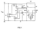
図1には、本発明による回路装置の実施例の略図が示されている。この回路装置には、第1入力端子E1と第2入力端子E2とが含まれており、これらの端子間に直流電圧が接続される。有利には、300〜400Vのオーダのいわゆる中間回路電圧が接続される。入力端子E1,E2間にはDC低電圧給電ユニット10が接続されており、この給電ユニットは、第1の出力側A1においてマイクロコントローラ12に5Vの直流電圧を供給し、また第2の出力側A2においてハイサイドドライバ14およびローサイドドライバ16に15Vの直流電圧を供給する。マイクロコントローラ12は、ローサイドドライバ16を直接駆動制御し、また電位分離ユニット18を介してハイサイドドライバを駆動制御する。
Advantageous Embodiments of the Invention FIG. 1 shows a schematic representation of an embodiment of a circuit arrangement according to the invention. This circuit device includes a first input terminal E1 and a second input terminal E2, and a DC voltage is connected between these terminals. Advantageously, a so-called intermediate circuit voltage on the order of 300-400 V is connected. A DC low voltage
DC低電圧給電ユニット10の出力側A2とハイサイドドライバ14との間にはチャージポンプが接続されており、このチャージポンプにはダイオードD1およびコンデンサC1が含まれている。コンデンサC1は、交流電圧源に接続されており、これはここではブリッジ回路20のブリッジ中間点BM1である。ブリッジ中間点BM1の電位は、基準電位としてハイサイドドライバ14に供給されるのに対して、ローサイドドライバ16は、基準電位としてアース電位を受け取る。このアース電位は、入力端子E2における電位である。
A charge pump is connected between the output side A2 of the DC low voltage
ブリッジ回路20には4つの電子スイッチS1,S2,S3,S4が含まれており、動作時には対角線S1,S4のスイッチが公知のように同時に開かれるのに対して、別の対角線S2,S3のスイッチが閉じられる。またこの逆が行われる。高圧放電ランプLaは、互いに接続された2つのインダクタンスL1,L2と、コンデンサC2とを含む点火回路を介して、2つのブリッジ中間点BM1,BM2間に接続されている。
The
ハイサイドドライバ14は、スイッチS1,S3の駆動制御に使用されるのに対して、ローサイドドライバ16は、スイッチS2,S4の駆動制御に使用される。
The
したがってブリッジ中間点BM1の電位は、スイッチS1,S2の位置に依存して0VとUZWとに切り換わる。ハイサイドドライバ14を給電するためのコンデンサC1の再充電が可能になるのは、ブリッジ中間点BM1がアース電位にある場合、すなわち、スイッチS2が閉じられておりかつスイッチS1が開いている場合である。
Therefore, the potential at the bridge intermediate point BM1 is switched between 0 V and U ZW depending on the positions of the switches S1 and S2. Recharging of the capacitor C1 for supplying power to the
放電ランプLaにDC信号を供給するため、連続する2つずつの転流が、高速に相前後して実施される2つの転流、いわゆる擬似転流によって複数回相前後して置き換えられる。これによってランプLaにDC信号が供給され続ける。それは、点火回路の出力キャパシタンスおよび出力インダクタンスにより、ランプ電流は十分な速度でその向きを変えることができないからである。ここではランプ電流の振幅の一時的な落ち込みだけが確認される。 In order to supply a DC signal to the discharge lamp La, two successive commutations are replaced by two or more successive commutations performed at a high speed in succession, so-called pseudo commutation. As a result, the DC signal is continuously supplied to the lamp La. This is because the output current and output inductance of the ignition circuit prevents the lamp current from changing its direction at a sufficient rate. Here, only a temporary drop in the amplitude of the lamp current is confirmed.
図示しない1実施形態では、擬似転流を上記のように実施する代わりに、電源部および転流器を介してランプLaにDC信号が供給される。ここでこの供給は、ランプに供給される出力が低下して、AC信号によるランプの動作時にランプのアークが消える危険性があると直ちに行われる。 In one embodiment (not shown), instead of performing the pseudo commutation as described above, a DC signal is supplied to the lamp La via the power supply unit and the commutator. Here, this supply is performed immediately when the output supplied to the lamp decreases and there is a risk that the arc of the lamp disappears during operation of the lamp by the AC signal.
図2には、高圧放電ランプLaに供給される出力Pの時間経過が略示されている。時点t0とt1との間、ランプは通常動作において100%の出力で作動される。オペレータは、時点t1に高圧放電ランプLaが取り付けられているプロジェクタをオフにすることを望んでいる。マイクロコントローラ12には、図1に示していないインタフェースを介して相応する信号が供給され、これに基づき、本発明による回路装置は、ランプLaに供給される出力を制御して低下させ始める。時点t0とt2との間、高圧放電ランプLaはAC信号によって作動される。時点t2において、すなわち、AC信号で引き続けて作動させるとランプのアークが消えてしまう危険性がある出力閾値に達すると、AC動作から擬似DC動作に切り換えられる。このために高電圧放電ランプLaをいわゆる擬似転流で作動させる。ここではランプに供給される出力をさらに低減して、時点t3までに、500Hzのオーダの周波数の擬似転流によってランプが作動されるいわゆるスタンバイ動作に達するようにする。これによって確実に、コンデンサC1が十分に再充電されて、ハイサイドドライバ14の正常な動作が保証されるようにする。時点t3とt4との間ではランプは、その定格出力の約20%で作動される。これによってランプは、さらに冷却されて、t1からt4までの時間幅を設定するか、またはランプ温度を測定することによって求められる時点t4には、スイッチオフ過程後に直ちに再点火に成功する温度に到達する。択一的に温度を測定する場合、あらかじめ設定した温度、例えば、350℃またはそれ以下にランプが冷却されたことによって時点t4を決定する。
FIG. 2 schematically shows the time course of the output P supplied to the high-pressure discharge lamp La. Between time t 0 and t 1, the lamp is operated at 100% output in the normal operation. The operator wants to turn off the projector high pressure discharge lamp La at the time t 1 is mounted. A corresponding signal is supplied to the
このようにすれば、オペレータが望めば、高圧放電ランプLaを時間窓ΔT1においていつでも直ちに再び100%にパワーアップすることができる。オペレータが望めば、時点ΔT2には、ランプLaを直ちに効果的に再点火することが可能である。したがってランプLaを直ちに再度オンにすることのできない時点はもはや存在しないのである。 In this way, if the operator desires, the high-pressure discharge lamp La can be immediately powered up again to 100% in the time window ΔT 1 at any time. If the operator desires, at time ΔT 2 , the lamp La can be immediately and effectively re-ignited. There is therefore no longer a point in time when the lamp La cannot be switched on again immediately.
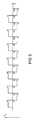
図3には、擬似転流が行われないランプ電流の時間経過が示されている。上記の転流には1〜14の番号が付されている。転流の直前にランプ電流はパルス状に増大する。これは、例えば、WO95/35645に記載されたフリッカ現象、殊にフリッカおよびアークジャンプ(Bogensprichen)を低減するための手段である。この手段は、本発明の1態様による擬似転流の実施とは無関係である。上で示した電流の矩形状の経過の周波数は、ふつう200Hz〜5kHzである。 FIG. 3 shows a time course of the lamp current in which the pseudo commutation is not performed. The commutations are numbered 1-14. Immediately before commutation, the lamp current increases in pulses. This is, for example, a means for reducing the flicker phenomenon described in WO 95/35645, in particular flicker and arc jump. This measure is independent of the implementation of simulated commutation according to one aspect of the present invention. The frequency of the rectangular shape of the current shown above is usually 200 Hz to 5 kHz.
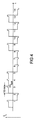
図4においてわかるのは、転流3,4および6,7がマイクロコントローラ12によって極めて短時間に行われていることである。ここでは長い転流15msであり、短い転流はわずかに5μsである。後者はランプ電流ILにおいてまったく識別できない。それは、この電流は、点火回路の出力キャパシタンスおよび出力インダクタンスのために、その流れる方向を高速には逆転できないからである。すなわち、このランプにはDC信号が供給されるのである。しかしながらこの短い転流は、チャージポンプのコンデンサを再充電するのには十分である。これに対して通常動作における典型的な転流には、有利な実施例において約50μsかかる。
It can be seen in FIG. 4 that the
Claims (10)
該回路装置は、高圧放電ランプ用の作動回路を有しており、
該作動回路は、高圧放電ランプ(La)用のスイッチオン/スイッチオフ信号を受信するための入力側と、作動信号を高圧放電ランプ(La)に供給するための少なくとも1つの出力側とを有している、
形式の回路装置において、
前記の作動回路は、その入力側にてスイッチオフ信号を受信した後、前記の少なくとも1つの出力側に供給される前記の作動信号の出力(P)を低減するように構成されており、
前記の作動回路はさらに、前記の作動信号を、あらかじめ設定可能な出力閾値以上ではAC信号として供給し、当該のあらかじめ設定可能な出力閾値以下では擬似DC信号として供給するように構成されており、
前記の駆動制御回路(12)は、スイッチオフの際に最後の擬似DC動作中の極性を記憶するように構成されており、
前記の駆動制御回路(12)はさらに、前記の擬似DC動作に対する次のスイッチオフの際に他方の極性を使用するように構成されている、
ことを特徴とする、高圧放電ランプ(La)を作動させるための回路装置。 A circuit device for operating a high-pressure discharge lamp (La),
The circuit device has an operating circuit for a high-pressure discharge lamp,
The operating circuit has an input side for receiving a switch-on / switch-off signal for the high-pressure discharge lamp (La) and at least one output side for supplying an operating signal to the high-pressure discharge lamp (La). It is,
In a circuit device of the type
Actuating said circuit, after receiving the switch-off signal at its input side and been configured to reduce the output (P) of the previous SL least one of said actuation signal supplied to the output side of the ,
Before SL actuation circuit further said actuation signal, supplied as AC signal at a pre-settable or output threshold, below the preset possible output thresholds been configured to supply a pseudo DC signal And
The drive control circuit (12) is configured to store the polarity during the last pseudo DC operation when the switch is turned off.
The drive control circuit (12) is further configured to use the other polarity at the next switch-off for the pseudo-DC operation,
A circuit device for operating a high-pressure discharge lamp (La).
前記の作動回路にはさらに少なくとも前記の第1電子スイッチ(S1)および第2電子スイッチ(S2)用の駆動制御回路(14,16)が含まれており、
該駆動制御回路(14,16)は、少なくとも前記の第1電子スイッチ(S1)および第2電子スイッチ(S2)を、前記のブリッジ回路(20)の出力側に少なくとも前記のAC信号を供給するよう制御するように構成されている、
請求項1に記載の回路装置。 The operating circuit includes a bridge circuit (20) having at least one first electronic switch (S1) and a second electronic switch (S2),
Contains further at least the first electronic switch (S1) and the second drive control circuit for an electronic switch (S2) (14,16) to said actuation circuit,
The drive control circuit (14, 16) is to supply at least the AC signal of at least the first electronic switch (S1) and a second electronic switch (S2), the output side of said bridge circuit (20) Configured to control ,
The circuit device according to claim 1.
当該作動回路は、前記のあらかじめ定めた出力閾値以下では前記の出力側と、前記の直流電源とを接続するように構成されている、
請求項1または2に記載の回路装置。 The operating circuit includes a DC voltage source,
Those the actuation circuit comprises of the following predetermined power threshold and the output side of the, has been configured to connect the DC power source,
The circuit device according to claim 1.
請求項2に記載の回路装置。 Before SL of the drive control circuit (14, 16) further said at least a first electronic switch (S1) and the second electronic stitching (S2), the pseudo DC signals to an output side of the bridge circuit (20) is configured so as also so that control be supplied,
The circuit device according to claim 2.
請求項4に記載の回路装置。 Said drive control circuit (14, 16), by shortening the commutation time, i.e., has been configured to provide a pseudo DC signal of the by the so-called pseudo commutation,
The circuit device according to claim 4.
前記のローサイドドライバ(16)およびハイサイドドライバ(14)は、前記の各電子スイッチ(S1;S2)と接続するための1つずつの出力側と、制御装置(12)と接続するための1つずつの制御入力側と、給電電圧を接続するための端子に接続するための1つずつの給電端子とを有しており、
前記のハイサイドドライバ(14)にはコンデンサ(C1)が割り当てられて設けられており、
該コンデンサは、前記の第1電子スイッチ(S1)と第2電子スイッチ(S2)との間の中間点(BM1)と、前記の給電端子との間に接続されている、
請求項1から5までのいずれか1項に記載の回路装置。 The drive control circuit includes a low-side driver (16) and a high-side driver (14) for at least the first electronic switch (S1) and the second electronic switch (S2),
The low-side driver (16) and the high-side driver (14) include one output side for connecting to the electronic switches (S1; S2) and one for connecting to the control device (12). Each having a control input side and one feed terminal for connecting to a terminal for connecting a feed voltage,
The high side driver (14) is provided with a capacitor (C1),
The capacitor is connected between an intermediate point (BM1) between the first electronic switch (S1) and the second electronic switch (S2) and the feeding terminal.
The circuit device according to any one of claims 1 to 5.
該ダイオードは、前記のコンデンサ(C1)から前記の給電電圧端子への電流が阻止されるように、前記のコンデンサ(C1)と前記の給電電圧端子との間に接続されている、
請求項6に記載の回路装置。 The drive control circuit (14; 16) further includes a diode (D1),
The diode is connected between the capacitor (C1) and the power supply voltage terminal so that a current from the capacitor (C1) to the power supply voltage terminal is blocked .
The circuit device according to claim 6.
請求項5から7までのいずれか1項に記載の回路装置。 The drive control circuit (14, 16) is configured to perform the pseudo-commutation at a frequency between 50 Hz and 1 kHz, preferably at a frequency of 500 Hz.
The circuit device according to any one of claims 5 to 7 .
前記の駆動制御回路(14,16)はさらに、前記の高圧放電ランプ(La)があらかじめ設定可能な出力の擬似DC信号で駆動されるあらかじめ設定した時間の経過後、前記の高圧放電ランプ(La)の動作を調整するように構成されている、
請求項1から8までのいずれか1項に記載の回路装置。 Further, the drive control circuit (14, 16) includes a time measuring device,
Said drive control circuit (14, 16) further after the elapse of the high-pressure discharge lamp (La) is a preset time which is driven by a pseudo DC signals presettable output of the previous SL pressure discharge lamp ( has been configured to adjust the operation of la),
The circuit device according to any one of claims 1 to 8 .
前記の回路装置は、高圧放電ランプ(La)用の作動回路を有しており、
該作動回路は、前記の高圧放電ランプ(La)用のスイッチオン/スイッチオフ信号を受信するための入力側と、作動信号を前記の高圧放電ランプ(La)に供給するための少なくとも1つの出力側とを有している、
形式の方法において、
該方法は以下のステップ、すなわち、
a) 前記の作動回路の入力側にてスイッチオフ信号を受信するステップと、
b) 前記の作動回路の少なくとも1つの出力側に供給される作動信号の出力を低減するステップであって、この際、あらかじめ設定可能な出力閾値以上ではAC信号として、また当該のあらかじめ設定可能な出力閾値以下では擬似DC信号として前記の作動信号を供給するステップと、
を含み、
スイッチオフの際に最後の擬似DC動作中の極性が記憶され、
前記の擬似DC動作に対する次のスイッチオフの際に他方の極性が使用される、
ことを特徴とする、回路装置にて高圧放電ランプ(La)を作動させる方法。 A method of operating a high pressure discharge lamp (La) in a circuit device,
The circuit device has an operating circuit for a high-pressure discharge lamp (La),
The operating circuit has an input for receiving a switch-on / switch-off signal for the high-pressure discharge lamp (La) and at least one output for supplying an operating signal to the high-pressure discharge lamp (La). Having a side ,
In the form method,
The method comprises the following steps:
a) receiving a switch-off signal on the input side of the actuation circuit;
b) a step of reducing the output of the actuation signal supplied to at least one output side of the actuation circuit, wherein the signal is above the preset output threshold value as an AC signal and can be set in advance Supplying the actuation signal as a pseudo DC signal below an output threshold ;
Including
When switching off, the polarity during the last pseudo DC operation is stored,
The other polarity is used at the next switch-off for said pseudo-DC operation,
A method for operating a high pressure discharge lamp (La) in a circuit arrangement.
Applications Claiming Priority (1)
| Application Number | Priority Date | Filing Date | Title |
|---|---|---|---|
| PCT/EP2007/062269 WO2009062542A1 (en) | 2007-11-13 | 2007-11-13 | Circuit assembly and method for operating a high pressure discharge lamp |
Publications (2)
| Publication Number | Publication Date |
|---|---|
| JP2011503810A JP2011503810A (en) | 2011-01-27 |
| JP5249342B2 true JP5249342B2 (en) | 2013-07-31 |
Family
ID=39618828
Family Applications (1)
| Application Number | Title | Priority Date | Filing Date |
|---|---|---|---|
| JP2010533441A Expired - Fee Related JP5249342B2 (en) | 2007-11-13 | 2007-11-13 | Circuit apparatus and method for operating a high pressure discharge lamp |
Country Status (7)
| Country | Link |
|---|---|
| US (1) | US8593072B2 (en) |
| EP (1) | EP2210454A1 (en) |
| JP (1) | JP5249342B2 (en) |
| KR (1) | KR20100098631A (en) |
| CN (1) | CN101855945B (en) |
| TW (1) | TW200932052A (en) |
| WO (1) | WO2009062542A1 (en) |
Families Citing this family (4)
| Publication number | Priority date | Publication date | Assignee | Title |
|---|---|---|---|---|
| US8901344B2 (en) | 2008-12-16 | 2014-12-02 | Basf Se | Production of carboxylic acid esters by stripping with alcohol vapor |
| US8472865B2 (en) * | 2010-08-12 | 2013-06-25 | Babak Taherloo | Echo light complex |
| WO2012120435A2 (en) * | 2011-03-10 | 2012-09-13 | Koninklijke Philips Electronics N.V. | A method of driving a gas-discharge lamp |
| KR101360685B1 (en) * | 2012-05-31 | 2014-02-10 | 엘지이노텍 주식회사 | Illumination system reduced standby power |
Family Cites Families (28)
| Publication number | Priority date | Publication date | Assignee | Title |
|---|---|---|---|---|
| TW339496B (en) | 1994-06-22 | 1998-09-01 | Philips Electronics Nv | Method and circuit arrangement for operating a high-pressure discharge lamp |
| US5523405A (en) * | 1995-03-14 | 1996-06-04 | E. I. Du Pont De Nemours And Company | Preparation of 4,6-dimethoxy-2-((phenoxycarbonyl)amino)-pyrimidine |
| US5932976A (en) * | 1997-01-14 | 1999-08-03 | Matsushita Electric Works R&D Laboratory, Inc. | Discharge lamp driving |
| EP1057375B1 (en) * | 1998-12-21 | 2003-10-15 | Koninklijke Philips Electronics N.V. | Circuit arrangement |
| US6329761B1 (en) * | 2000-06-30 | 2001-12-11 | Ebs International Corporation | Frequency controlled half-bridge inverter for variable loads |
| JP4070420B2 (en) * | 2001-03-23 | 2008-04-02 | フェニックス電機株式会社 | Ultra high pressure discharge lamp lighting method and lighting device |
| EP1389036A4 (en) * | 2001-05-16 | 2004-06-23 | Matsushita Electric Industrial Co Ltd | DISCHARGE LAMP LIGHTING DEVICE AND SYSTEM COMPRISING THE SAME |
| JP3948233B2 (en) | 2001-10-01 | 2007-07-25 | 株式会社村田製作所 | Multilayer electronic component and manufacturing method thereof |
| DE10220509A1 (en) * | 2002-05-08 | 2003-11-20 | Philips Intellectual Property | Method and circuit arrangement for operating a high-pressure gas discharge lamp |
| JP4241615B2 (en) * | 2002-06-25 | 2009-03-18 | コーニンクレッカ フィリップス エレクトロニクス エヌ ヴィ | Discharge lamp operation |
| US7316483B2 (en) * | 2003-01-15 | 2008-01-08 | Koninklijke Philips Electronics N.V. | Method of representing a video image by means of a projector |
| JP3870914B2 (en) * | 2003-02-28 | 2007-01-24 | ウシオ電機株式会社 | Excimer lamp light emitting device |
| US7187244B2 (en) * | 2003-03-03 | 2007-03-06 | International Rectifier Corporation | Digital light ballast oscillator |
| JP2004319193A (en) * | 2003-04-15 | 2004-11-11 | Phoenix Denki Kk | Lighting method and lighting device of high-pressure discharge lamp, and image apparatus using it |
| JP4023413B2 (en) * | 2003-07-28 | 2007-12-19 | 松下電工株式会社 | High pressure discharge lamp lighting device |
| JP4440614B2 (en) * | 2003-12-05 | 2010-03-24 | フェニックス電機株式会社 | High pressure discharge lamp lighting method, lighting device, and video equipment using the lighting device |
| US7619369B2 (en) * | 2003-12-19 | 2009-11-17 | Koninklijke Philips Electronics N.V. | Method and circuit arrangement for operating a discharge lamp |
| JP2005190766A (en) * | 2003-12-25 | 2005-07-14 | Ushio Inc | High pressure discharge lamp lighting device and projector device |
| JP4448396B2 (en) * | 2004-07-13 | 2010-04-07 | 株式会社日立製作所 | Lamp operation control device and method thereof |
| JP2008507815A (en) * | 2004-07-21 | 2008-03-13 | コーニンクレッカ フィリップス エレクトロニクス エヌ ヴィ | Lamp driver that provides synchronization during commutation |
| CN100576418C (en) | 2004-08-02 | 2009-12-30 | 优志旺电机株式会社 | High pressure discharge lamp lighting device |
| JP4990490B2 (en) | 2004-11-11 | 2012-08-01 | パナソニック株式会社 | High pressure discharge lamp lighting device, high pressure discharge lamp device, projection-type image display device, and high pressure discharge lamp lighting method |
| JP4711742B2 (en) * | 2005-05-26 | 2011-06-29 | フェニックス電機株式会社 | Lighting method of high pressure discharge lamp |
| US7443103B2 (en) * | 2005-06-24 | 2008-10-28 | General Electric Company | High pressure lamp with lamp flicker suppression and lamp voltage control |
| US7323827B2 (en) * | 2005-12-29 | 2008-01-29 | General Electric Company | Ripple reduction method for electronic ballasts |
| JP2007214010A (en) * | 2006-02-10 | 2007-08-23 | Seiko Epson Corp | Discharge lamp lighting device and projector |
| JP5073682B2 (en) * | 2006-02-20 | 2012-11-14 | コーニンクレッカ フィリップス エレクトロニクス エヌ ヴィ | Method and drive unit for driving a gas discharge lamp |
| KR101358178B1 (en) * | 2006-12-13 | 2014-02-07 | 오스람 게엠베하 | Circuit arrangement for operation of discharge lamps, and method for operation of discharge lamps |
-
2007
- 2007-11-13 JP JP2010533441A patent/JP5249342B2/en not_active Expired - Fee Related
- 2007-11-13 CN CN200780101538XA patent/CN101855945B/en not_active Expired - Fee Related
- 2007-11-13 WO PCT/EP2007/062269 patent/WO2009062542A1/en not_active Ceased
- 2007-11-13 KR KR1020107013096A patent/KR20100098631A/en not_active Ceased
- 2007-11-13 US US12/742,447 patent/US8593072B2/en not_active Expired - Fee Related
- 2007-11-13 EP EP07822542A patent/EP2210454A1/en not_active Withdrawn
-
2008
- 2008-11-04 TW TW097142485A patent/TW200932052A/en unknown
Also Published As
| Publication number | Publication date |
|---|---|
| WO2009062542A1 (en) | 2009-05-22 |
| JP2011503810A (en) | 2011-01-27 |
| TW200932052A (en) | 2009-07-16 |
| KR20100098631A (en) | 2010-09-08 |
| US20100270934A1 (en) | 2010-10-28 |
| CN101855945B (en) | 2013-10-23 |
| CN101855945A (en) | 2010-10-06 |
| US8593072B2 (en) | 2013-11-26 |
| EP2210454A1 (en) | 2010-07-28 |
Similar Documents
| Publication | Publication Date | Title |
|---|---|---|
| JP4052039B2 (en) | High pressure discharge lamp lighting device | |
| JP5073682B2 (en) | Method and drive unit for driving a gas discharge lamp | |
| CN101686594B (en) | High pressure discharge lamp lighting device and luminaire using the same | |
| JP5264713B2 (en) | Lamp drive circuit | |
| WO2004103032A1 (en) | Device and method for lighting high-voltage discharge lamp | |
| WO2008001519A1 (en) | Electric discharge lamp device and lighting apparatus | |
| JP5249342B2 (en) | Circuit apparatus and method for operating a high pressure discharge lamp | |
| JP4438617B2 (en) | Power supply device for high-pressure discharge lamp | |
| CN1572125A (en) | Circuit arrangement for operating a discharge lamp | |
| US8664872B2 (en) | Circuit arrangement for operating a discharge lamp | |
| JP5262647B2 (en) | High pressure discharge lamp lighting device, projector, and high pressure discharge lamp starting method | |
| JP4088816B2 (en) | Lighting device and lighting device | |
| JP4969583B2 (en) | Discharge lamp lighting device and projector | |
| JP5460065B2 (en) | Discharge lamp lighting circuit | |
| EP1897418A2 (en) | Method for driving an inverter of a gas discharge supply circuit | |
| JP2011505659A (en) | Method and apparatus for igniting a gas discharge lamp | |
| JP4460106B2 (en) | How to turn on the high-pressure discharge lamp | |
| CN101982020B (en) | Circuit arrangement for operating HID discharge lamps | |
| JP2010080137A (en) | High pressure discharge lamp lighting device and luminaire | |
| JP2010080138A (en) | High-pressure discharge lamp lighting device, and lighting fixture | |
| JP2013201030A (en) | High-pressure discharge lamp lighting device and projector using the same | |
| US8917036B1 (en) | Method and apparatus for dimming high intensity discharge lamps | |
| JP2002237393A (en) | Discharge lamp lighting device | |
| KR200179879Y1 (en) | Series type ignitor for high-intensity discharge lamp | |
| JP2009224080A (en) | Discharge lamp lighting device |
Legal Events
| Date | Code | Title | Description |
|---|---|---|---|
| RD04 | Notification of resignation of power of attorney |
Free format text: JAPANESE INTERMEDIATE CODE: A7424 Effective date: 20101228 |
|
| A977 | Report on retrieval |
Free format text: JAPANESE INTERMEDIATE CODE: A971007 Effective date: 20120309 |
|
| A131 | Notification of reasons for refusal |
Free format text: JAPANESE INTERMEDIATE CODE: A131 Effective date: 20120328 |
|
| A601 | Written request for extension of time |
Free format text: JAPANESE INTERMEDIATE CODE: A601 Effective date: 20120625 |
|
| A602 | Written permission of extension of time |
Free format text: JAPANESE INTERMEDIATE CODE: A602 Effective date: 20120702 |
|
| A601 | Written request for extension of time |
Free format text: JAPANESE INTERMEDIATE CODE: A601 Effective date: 20120726 |
|
| A602 | Written permission of extension of time |
Free format text: JAPANESE INTERMEDIATE CODE: A602 Effective date: 20120802 |
|
| A601 | Written request for extension of time |
Free format text: JAPANESE INTERMEDIATE CODE: A601 Effective date: 20120827 |
|
| A602 | Written permission of extension of time |
Free format text: JAPANESE INTERMEDIATE CODE: A602 Effective date: 20120903 |
|
| A521 | Request for written amendment filed |
Free format text: JAPANESE INTERMEDIATE CODE: A523 Effective date: 20120921 |
|
| TRDD | Decision of grant or rejection written | ||
| A01 | Written decision to grant a patent or to grant a registration (utility model) |
Free format text: JAPANESE INTERMEDIATE CODE: A01 Effective date: 20130313 |
|
| A61 | First payment of annual fees (during grant procedure) |
Free format text: JAPANESE INTERMEDIATE CODE: A61 Effective date: 20130411 |
|
| R150 | Certificate of patent or registration of utility model |
Free format text: JAPANESE INTERMEDIATE CODE: R150 |
|
| FPAY | Renewal fee payment (event date is renewal date of database) |
Free format text: PAYMENT UNTIL: 20160419 Year of fee payment: 3 |
|
| LAPS | Cancellation because of no payment of annual fees |