JP5243550B2 - Method and device for processing silicon wafers - Google Patents
Method and device for processing silicon wafers Download PDFInfo
- Publication number
- JP5243550B2 JP5243550B2 JP2010538475A JP2010538475A JP5243550B2 JP 5243550 B2 JP5243550 B2 JP 5243550B2 JP 2010538475 A JP2010538475 A JP 2010538475A JP 2010538475 A JP2010538475 A JP 2010538475A JP 5243550 B2 JP5243550 B2 JP 5243550B2
- Authority
- JP
- Japan
- Prior art keywords
- silicon wafer
- etching solution
- texturing
- etching
- polishing
- Prior art date
- Legal status (The legal status is an assumption and is not a legal conclusion. Google has not performed a legal analysis and makes no representation as to the accuracy of the status listed.)
- Active
Links
Images

Classifications
-
- H—ELECTRICITY
- H01—ELECTRIC ELEMENTS
- H01L—SEMICONDUCTOR DEVICES NOT COVERED BY CLASS H10
- H01L21/00—Processes or apparatus adapted for the manufacture or treatment of semiconductor or solid state devices or of parts thereof
- H01L21/67—Apparatus specially adapted for handling semiconductor or electric solid state devices during manufacture or treatment thereof; Apparatus specially adapted for handling wafers during manufacture or treatment of semiconductor or electric solid state devices or components ; Apparatus not specifically provided for elsewhere
- H01L21/67005—Apparatus not specifically provided for elsewhere
- H01L21/67011—Apparatus for manufacture or treatment
- H01L21/67017—Apparatus for fluid treatment
- H01L21/67063—Apparatus for fluid treatment for etching
- H01L21/67075—Apparatus for fluid treatment for etching for wet etching
- H01L21/6708—Apparatus for fluid treatment for etching for wet etching using mainly spraying means, e.g. nozzles
-
- B—PERFORMING OPERATIONS; TRANSPORTING
- B05—SPRAYING OR ATOMISING IN GENERAL; APPLYING FLUENT MATERIALS TO SURFACES, IN GENERAL
- B05C—APPARATUS FOR APPLYING FLUENT MATERIALS TO SURFACES, IN GENERAL
- B05C1/00—Apparatus in which liquid or other fluent material is applied to the surface of the work by contact with a member carrying the liquid or other fluent material, e.g. a porous member loaded with a liquid to be applied as a coating
- B05C1/02—Apparatus in which liquid or other fluent material is applied to the surface of the work by contact with a member carrying the liquid or other fluent material, e.g. a porous member loaded with a liquid to be applied as a coating for applying liquid or other fluent material to separate articles
- B05C1/025—Apparatus in which liquid or other fluent material is applied to the surface of the work by contact with a member carrying the liquid or other fluent material, e.g. a porous member loaded with a liquid to be applied as a coating for applying liquid or other fluent material to separate articles to flat rectangular articles, e.g. flat sheets
-
- B—PERFORMING OPERATIONS; TRANSPORTING
- B05—SPRAYING OR ATOMISING IN GENERAL; APPLYING FLUENT MATERIALS TO SURFACES, IN GENERAL
- B05C—APPARATUS FOR APPLYING FLUENT MATERIALS TO SURFACES, IN GENERAL
- B05C1/00—Apparatus in which liquid or other fluent material is applied to the surface of the work by contact with a member carrying the liquid or other fluent material, e.g. a porous member loaded with a liquid to be applied as a coating
- B05C1/04—Apparatus in which liquid or other fluent material is applied to the surface of the work by contact with a member carrying the liquid or other fluent material, e.g. a porous member loaded with a liquid to be applied as a coating for applying liquid or other fluent material to work of indefinite length
- B05C1/08—Apparatus in which liquid or other fluent material is applied to the surface of the work by contact with a member carrying the liquid or other fluent material, e.g. a porous member loaded with a liquid to be applied as a coating for applying liquid or other fluent material to work of indefinite length using a roller or other rotating member which contacts the work along a generating line
- B05C1/0813—Apparatus in which liquid or other fluent material is applied to the surface of the work by contact with a member carrying the liquid or other fluent material, e.g. a porous member loaded with a liquid to be applied as a coating for applying liquid or other fluent material to work of indefinite length using a roller or other rotating member which contacts the work along a generating line characterised by means for supplying liquid or other fluent material to the roller
-
- H—ELECTRICITY
- H01—ELECTRIC ELEMENTS
- H01L—SEMICONDUCTOR DEVICES NOT COVERED BY CLASS H10
- H01L21/00—Processes or apparatus adapted for the manufacture or treatment of semiconductor or solid state devices or of parts thereof
- H01L21/67—Apparatus specially adapted for handling semiconductor or electric solid state devices during manufacture or treatment thereof; Apparatus specially adapted for handling wafers during manufacture or treatment of semiconductor or electric solid state devices or components ; Apparatus not specifically provided for elsewhere
- H01L21/67005—Apparatus not specifically provided for elsewhere
- H01L21/67011—Apparatus for manufacture or treatment
- H01L21/67017—Apparatus for fluid treatment
- H01L21/67063—Apparatus for fluid treatment for etching
- H01L21/67075—Apparatus for fluid treatment for etching for wet etching
- H01L21/67086—Apparatus for fluid treatment for etching for wet etching with the semiconductor substrates being dipped in baths or vessels
-
- H—ELECTRICITY
- H01—ELECTRIC ELEMENTS
- H01L—SEMICONDUCTOR DEVICES NOT COVERED BY CLASS H10
- H01L21/00—Processes or apparatus adapted for the manufacture or treatment of semiconductor or solid state devices or of parts thereof
- H01L21/67—Apparatus specially adapted for handling semiconductor or electric solid state devices during manufacture or treatment thereof; Apparatus specially adapted for handling wafers during manufacture or treatment of semiconductor or electric solid state devices or components ; Apparatus not specifically provided for elsewhere
- H01L21/67005—Apparatus not specifically provided for elsewhere
- H01L21/67011—Apparatus for manufacture or treatment
- H01L21/6715—Apparatus for applying a liquid, a resin, an ink or the like
Abstract
Description
本発明は、シリコンウエハを処理するための方法に関し、またシリコンウエハを処理するためのデバイスに関し、特には、エッチング溶液でテクスチャリング及び研磨エッチングをするための方法、並びにデバイスに関する。 The present invention relates to a method for processing a silicon wafer, and to a device for processing a silicon wafer, and more particularly to a method and device for texturing and polishing etching with an etching solution.
実務として、エッチング溶液を用いてシリコンウエハの両面からそのシリコンウエハのおよそ5μmをエッチングすることが従来知られている。それによって、第一に切断損傷を取り除くことが可能である。さらに、テクスチャー化した上面を作製することが可能であり、そのテクスチャー化した上面はシリコンウエハから生産される太陽電池の性能に対して重要である。さらにその上、通過した光が反射されてそのエネルギーが戻り行程の途上で利用されるように、その下面は出来るだけ滑り性があって光沢性があるべきである。 In practice, it is conventionally known to etch about 5 μm of a silicon wafer from both sides of the silicon wafer using an etching solution. Thereby, it is possible to first remove the cutting damage. Furthermore, it is possible to produce a textured top surface, which is important for the performance of solar cells produced from silicon wafers. Furthermore, the lower surface should be as slippery and glossy as possible so that the light that passes through is reflected and its energy is utilized during the return stroke.
本発明は、前述した方法、さらにその方法を実行するための前述のデバイスを提供することを目的とし、その方法及びデバイスを利用して、先行技術での問題を解決することが可能であり、特には、好ましい更なる開発が可能である。そして、本発明はまた、改良されて効率的なシリコンウエハのエッチングを提供することを目的とする。 The present invention aims to provide the above-described method and the above-described device for performing the method, and the method and device can be used to solve the problems in the prior art. Particularly preferred further developments are possible. The present invention also aims to provide an improved and efficient etching of silicon wafers.
この目的は請求項1に記載の特徴部分を含む方法によって達成され、また、請求項10に記載の特徴部分を含むデバイスによって達成される。有利であって、かつ、好ましい本発明の実施形態は、その他の請求項に係る発明の主題であり、下記に詳細に述べられる。デバイスの幾つかの特徴部分は本発明の方法に関連して主に述べられるが、それらのデバイスの特徴部分はデバイスを説明するのに同時に役に立ち、一般的には、そのデバイスに適用可能である。さらに、同一出願人であって、2007年12月19日の優先権出願であるDE 102007063202.0号の記述は、参照することによって本明細書の記載の中身に組み込まれる。そのクレームの記述は参照することによって本明細書の記載の中身に組み込まれる。 This object is achieved by a method comprising the feature part of claim 1 and by a device comprising the feature part of claim 10. Advantageous and preferred embodiments of the invention are the subject matter of the other claimed inventions and are described in detail below. Although some features of the device are mainly described in connection with the method of the present invention, those device features are useful at the same time to describe the device and are generally applicable to that device. . Furthermore, the description of DE 102007063202.0, which is the same applicant and is a priority application as of December 19, 2007, is hereby incorporated by reference into the contents of this description. The claims description is incorporated by reference into the contents of this description.
本発明によれば、第一方法の段階で、シリコンウエハが水平位置の状態で搬送されて水平な搬送路に正確に沿って搬送されることが提供される。テクスチャリングのためのエッチング溶液が上方から塗布されるか又は噴霧されて、その目的のために、ノズル、サージパイプ等が用いられてよく、それら自体はそのような目的のために公知である。この方法の段階において、シリコンウエハの下方から、液体がシリコンウエハ又はそのシリコンウエハの下面に全く塗布されないか、又は少しの液体しか塗布されない。いずれにせよ、エッチング溶液は噴霧されないし、その下面からも同様である。この目的のために、それ相応の適切な方法で具現化されたデバイスは、上面をウェット状態にするために、搬送路の上方にノズル、サージパイプ等を有してよい。下面の下方には、そのようなノズル等は全く提供されない。 According to the present invention, it is provided that the silicon wafer is transported in a horizontal position and transported accurately along a horizontal transport path at the stage of the first method. Etching solutions for texturing may be applied or sprayed from above, and nozzles, surge pipes, etc. may be used for that purpose, which are known per se for such purposes. In this method step, from below the silicon wafer, no liquid is applied to the silicon wafer or the lower surface of the silicon wafer, or only a small amount of liquid is applied. In any case, the etching solution is not sprayed, and the same applies from the lower surface. For this purpose, a device embodied in a correspondingly appropriate way may have a nozzle, a surge pipe, etc. above the conveying path in order to make the upper surface wet. No such nozzle or the like is provided below the lower surface.
その後の又は第二の方法の段階において、同様な方法又は第一方法の段階と同様な配向で、搬送路に対して水平位置の状態のシリコンウエハは、下方からの研磨-エッチングのためのエッチング溶液でウェット化される。有利なこととして、この場合、エッチング溶液は、実際のところ下方だけから塗布され、そしてまた、下面にだけ塗布される。このことは、まさに、搬送ローラー等が搬送路のために用いられるならば、第一方法の段階で、上方からのエッチング溶液が搬送ローラー上でも通過することが可能であり、その後、搬送ローラーによってシリコンウエハの下面に搬送され得るという理由のためである。ところが、これは管理可能な量なので、ここにおけるエッチング効果は非常に小さいままの状態の可能性が高い。そのことは、例えば、第二方法の段階に対する生産においては有利にさえなる。 In the subsequent or second method stage, the silicon wafer in a horizontal position with respect to the transfer path in the same orientation as in the same method or the first method stage is etched for polishing-etching from below. Wet with solution. Advantageously, in this case, the etching solution is actually applied only from below and also only on the lower surface. This is exactly the case in which if the transport roller or the like is used for the transport path, the etching solution from above can also pass over the transport roller in the first method stage, and then by the transport roller. This is because it can be transferred to the lower surface of the silicon wafer. However, since this is a manageable amount, the etching effect here is likely to remain very small. That is even advantageous, for example, in production for the second process stage.
この方法では、およそ4μm〜6μmの材料、好ましくはおよそ5μmの材料が、切断損傷を排除して上面をテクスチャリングするために第一方法の段階で取り除かれ得る。ここにおいて、その方法の継続時間はおよそ80〜120秒でよい。この場合に、有利なこととしては、シリコンウエハは搬送路上で連続的に動くか又は搬送路上を進み対応するテクスチャリングモジュールを通り抜ける。 In this method, approximately 4 μm to 6 μm material, preferably approximately 5 μm material, can be removed in the first method step in order to eliminate cutting damage and texture the top surface. Here, the duration of the method may be approximately 80-120 seconds. In this case, advantageously, the silicon wafer moves continuously on the transport path or travels on the transport path and passes through the corresponding texturing module.
第一方法の段階で、およそ2μmの材料が下面上で取り除かれるか又はエッチングされる。結果として、ここにおいても切断損傷の一部分はもうすでに取り除かれ、一方では、ここにおいては好ましくはない表面テクスチャリングは、正確に言うとまだ引き起こされていない。テクスチャリング方法の段階後は、シリコンウエハはリンスされてよく、好ましくは水でリンスされる。 In the first method step, approximately 2 μm of material is removed or etched on the lower surface. As a result, part of the cutting damage has already been removed here, while on the other hand, surface texturing, which is not preferred here, has not yet been caused exactly. After the texturing process step, the silicon wafer may be rinsed, preferably rinsed with water.
第一方法の段階のために用いられるエッチング溶液は、テクスチャリングのための通常のエッチング溶液でよく、好ましくはHF及びHNO3の混合物を含むエッチング溶液である。第一方法の段階において、又はその段階がテクスチャリングモジュールで実行される場合に、テクスチャリングのためのエッチング溶液は、搬送路に沿って逐次的に複数の領域に塗布され得る。有利なこととして、この目的のために、エッチング溶液を噴霧するためのノズル等の複数のグループが、搬送路に対して横方向に走るサージパイプ等に逐次的に、好ましく提供される。このことも、原則として公知である。 The etching solution used for the first method step may be a conventional etching solution for texturing, preferably an etching solution comprising a mixture of HF and HNO 3 . In the first method step, or when the step is performed in the texturing module, the etching solution for texturing can be applied sequentially to a plurality of regions along the transport path. Advantageously, for this purpose, a plurality of groups such as nozzles for spraying the etching solution are preferably provided sequentially, such as a surge pipe running transversely to the transport path. This is also known in principle.
テクスチャリングモジュールは、搬送路の下に収集トラフが提供されることが好ましく、放出したエッチング溶液は収集されて再利用され得る。第一方法の段階のテクスチャリングモジュールで、エッチング溶液でウェット状態にした後にシリコンウエハをリンスすることは、そのテクスチャリングモジュールで実行されることが好ましく、特には、そのテクスチャリングモジュールの端部で実行されることが好ましい。テクスチャリングモジュールのある部分は水でリンスをするために具体化されてよく、クリーングの経費が減るようにする意図であって、二つの液を別個独立にする目的のために、収集トラフはエッチング溶液のための収集トラフとは別個独立にここに提供される。シリコンウエハ上で水を用いてリンスすることの強度、すなわち、水の量は、エッチング溶液でウェット状態にするための量よりも相当に多くてよい。 The texturing module is preferably provided with a collection trough under the transport path, and the released etching solution can be collected and reused. In the first method stage texturing module, rinsing the silicon wafer after wetting with the etching solution is preferably performed in the texturing module, in particular at the end of the texturing module. Preferably it is performed. Some parts of the texturing module may be embodied to be rinsed with water, with the intention of reducing the cost of cleaning, and the collection trough is etched for the purpose of making the two liquids independent. Provided here separately from the collection trough for the solution. The strength of rinsing with water on the silicon wafer, i.e. the amount of water, may be considerably greater than the amount to wet with the etching solution.
有利なこととしては、シリコンウエハは、次の段階若しくは第二方法の段階まで直接的に、第一方法の段階後に動くか、又はテクスチャリングモジュールから動き、次の段階若しくは第二方法の段階は研磨-エッチングモジュールにて実行される。ここで、研磨-エッチングのためのエッチング溶液が塗布されて、シリコンウエハは、いずれにせよ連続的に搬送路を進み、研磨-エッチングモジュールを通過する。シリコンウエハはそのシリコンウエハの下面のみウェット状態になる。一つの例として、このことは下方からの僅かな噴霧によって達成され得る。DE 10 2005 062 528 A1号を参照すると明確にのべられているが、その文献にしたがった研磨-エッチングモジュールにおける方法及びデバイスがこの目的のために好ましく用いられる。この場合に、シリコンウエハのための搬送ローラーは、研磨エッチングのためのエッチング溶液を含有するバスに大部分浸漬される。回転時に、エッチング溶液はシリコンウエハの上面に接着して、その後シリコンウエハの下面に運搬され、そこで、研磨エッチングを実行する。このようにして、3μm〜10μmのエッチング除去が下面で達成されて、それによって、非常に良好な研磨エッチングが非常に良好な結果によって可能となり、平坦性かつ光沢性のある後面をもたらすこととなる。この方法の段階は、前処理の段階よりも幾分長く継続してよく、特にはおよそ200秒間継続してよい。しかもこの場合において、エッチング除去はその処理の継続時間によって決定され得る。研磨エッチングのために用いられるエッチング溶液は、テクスチャリングで用いられる溶液と同一であるが、HNO3の比率が大きい。エッチング処理は室温で実行されてよく、温度範囲は、およそ4℃〜およそ40℃まで拡張することができる。 Advantageously, the silicon wafer moves directly after the first method step or from the texturing module until the next step or second method step, and the next step or second method step is Performed in the polish-etch module. Here, an etching solution for polishing-etching is applied, and the silicon wafer continuously passes the transfer path anyway and passes through the polishing-etching module. The silicon wafer is wet only on the lower surface of the silicon wafer. As one example, this can be achieved by a slight spray from below. Although clearly mentioned with reference to DE 10 2005 062 528 A1, methods and devices in polishing-etching modules according to that document are preferably used for this purpose. In this case, the transfer roller for the silicon wafer is mostly immersed in a bath containing an etching solution for polishing etching. During rotation, the etching solution adheres to the top surface of the silicon wafer and is then transported to the bottom surface of the silicon wafer where it performs a polishing etch. In this way, an etching removal of 3 μm to 10 μm is achieved at the bottom surface, thereby allowing a very good polishing etch with very good results, resulting in a flat and glossy back surface. . This method step may last somewhat longer than the pretreatment step, in particular it may last approximately 200 seconds. Moreover, in this case, the etch removal can be determined by the duration of the process. The etching solution used for polishing etching is the same as that used for texturing, but the ratio of HNO 3 is large. The etching process may be performed at room temperature, and the temperature range can extend from approximately 4 ° C. to approximately 40 ° C.
これらの特徴及び更なる特徴は、特許請求の記載だけでなく、明細書の記載及び図面の記載からも明確に現れ、個々の特徴は、各々の場合において単独で実現されることも可能であるし、本発明の実施態様及び他の分野においてサブコンビネーションの形態の複数のものとして実現されることも可能であり、それらの特徴は、有利であって本質的に保護可能な実施態様を構成することが可能であり、それらの実施態様のための保護はここにおいて主張される。個々のセクション及び副題に出願を細分化することは、それに従って作成された記述の一般的な効力を制限するものではない。 These and further features appear clearly not only in the claims but also in the description and the drawings, and individual features can also be realized independently in each case However, embodiments of the present invention and other fields can also be realized as a plurality of sub-combinations, and these features constitute advantageous and essentially protectable embodiments. It is possible that protection for those embodiments is claimed here. Subdividing an application into individual sections and subtitles does not limit the general efficacy of the description prepared accordingly.
本発明の典型的な実施形態が図面に概略的に示されて、下記に更に詳細に説明される。図面については以下のとおりである。
図1は、搬送経路12を備えたテクスチャリングモジュール11を示し、その搬送経路12は従来の方法で複数の搬送ローラー13によって形成される。そのテクスチャリングモジュール11は収集トラフ16を含むハウジング15を有し、搬送経路12の入口18を左方向から有する。
FIG. 1 shows a texturing module 11 with a
収集トラフ16及び搬送経路12の上方から、複数のサージパイプ19が互いに平行に提供され、そのサージパイプは搬送経路12に対して横走してよい。そのサージパイプは、エッチング溶液21放出するノズル20を下向きに向ける。また、そのノズル20は当該技術分野の当業者にとって公知である。そのノズルは強固に並べられてもよいし、可動的でもよい。そのうえ、ある状況下においては、エッチング溶液21の放出が特定のプロファイルに達するために、ノズル20はまた、個々に又は群で活動的でよい。
A plurality of
シリコンウエハ22は、搬送経路12に沿った水平位の搬送ローラー13で搬送される。上面23は、後に、太陽電池の前面を形成し、そして、搬送ローラー13を押し付ける下面24はその太陽電池の後面を形成する。
The
図1から認識されるように、エッチング溶液21は、シリコンウエハ22の上面23にのみに放出される。その結果として、シリコンウエハ22又はその上面23のテクスチャリングは、主に、第一方法の段階のここで達成される。この場合において、当然のことながら、エッチング溶液21の一定量は、特にシリコンウエハ22の先端及びその先端のへりにあふれ出して、その後搬送ローラー13に流れ出ることは明確である。それから、搬送ローラー13上に横に配置するその後のシリコンウエハ22は、シリコンウエハの下面24においてもエッチング溶液でウェット状態になる。ところが、ここにおいては、エッチング溶液の量はかなり少なく、しかも、結果として達成されるエッチングの量はかなり少ない。ところが、図に示されているように、対象となる上方からのエッチング溶液21の塗布はノズル20の手段によって達成されるので、このことは、本発明の目的の範囲内で上方からエッチング溶液を塗布をすることとして表される。
As can be seen from FIG. 1, the
例えば、ノズル20が搬送ローラー13の上方に配列されるか、又は搬送ローラー13の後方に向かって配向されるかどうかを確立することは可能であり、結果として、実際にシリコンウエハ22が下方に存在しないならば、エッチング溶液21は搬送ローラー13に塗布され、次のシリコンウエハ22の下面24のウェットの度合いをエッチング溶液21で増大させる。ノズル20が異なる方向に配列されるか又は配向されるならば、この効果は相当に小さくなる。その上、下面でエッチングすることについてのこの効果は、さらに、ノズル20の目標とする動きによって影響され得るか、又はシリコンウエハ22の上面23におけるエッチング溶液21の目標とする放出によって影響され得る。
For example, it is possible to establish whether the
右方向に向かって連続するテクスチャリングモジュール11において、右寄りに示されたノズル20はエッチング溶液21を放出しないように設計されてよいが、むしろ、水またはリンス液を放出されるように設計され得る。それによって、シリコンウエハ22の上面23の領域のエッチング溶液21を洗浄することができる。セパレーター28は、この目的のために収集トラフ16に提供されて、浸漬するエッチング溶液21は、そのセパレーターの左側に配置され、エッチング溶液に対して少ない割合で混ぜられたリンス液26はそのセパレーターの右側に配置される。エッチング溶液21を塗布するためのノズル20を備える連続的なサージパイプ19の数は変更することが可能であり、好ましい搬送スピード及び処理の継続時間にしたがって変更させることができる。さらに、有利なこととして、シリコンウエハ22をリンスするために複数のノズル20にリンス液26を提供することが可能である。
In the texturing module 11 that continues to the right, the
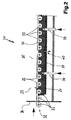
図2は、研磨-エッチングモジュール31を示す。このモジュールもまた、搬送経路32を有し、その搬送経路は図1の搬送経路12に対して連続的である。さらに、有利なこととして、研磨-エッチングモジュール31は、テクスチャリングモジュール11に対して連続した状態で比較的直接的に提供されて設置される。搬送経路32は搬送ローラー33によって形成される。研磨-エッチングモジュール31の詳細な記述に関しては、主に DE10 2005 062 528 A1号が参照され、その文献は、研磨-エッチングのためのエッチング溶液35が、搬送ローラー33の手段によってバス37からシリコンウエハ22の下面24まで如何に運搬されるかを詳細に述べている。それゆえに、搬送ローラーはウエハを搬送するためやウエハの下面を湿潤化するために役に立つ。研磨-エッチングのためのエッチング溶液35は上記で述べられたと同様である。また、第二方法の段階において、エッチング溶液35は、シリコンウエハ22の上面23を一切通り過ぎることはなく、むしろ下面24に到達する。
FIG. 2 shows a polishing-etching module 31. This module also has a
バス37は二つの供給パイプ38の間に排水口40を有し、それらのパイプは新しいエッチング溶液35をバス37に導入する。バス37のへりで外側に向かって液があふれ出ることに加えて、エッチング溶液35はそのような方法で交換されるので、フレッシュエッチング溶液35が供給パイプ38の出口の領域に存在するだけでなく、それらはまた排水口40の方向に動かされることをその排水口は保証し、それゆえ、搬送ローラー33によって、シリコンウエハ22の下面24までそのエッチング溶液は運搬される。また、シリコンウエハ22の処理の方法の順序として、研磨-エッチングモジュール31で研磨エッチングをした後に、続いて更にリンスが行われて、好ましくは水で再度もう1回濯ぐ。
The
また、研磨-エッチングモジュール31はハウジング34の中に提供される。勿論、エッチング溶液の蒸気の抽出が両方のモジュールで行われる。
A polishing-etching module 31 is also provided in the
基板は典型的には凹凸がなく平面状のシリコンウエハ22であり、そのシリコンウエハ22は、およそ60mm〜250mmの径を有した円形の輪郭を有するか、又は60mm〜250mmの稜線長を有した矩形の輪郭を有する。好ましい厚みは0.1mm〜2mmの範囲である。
The substrate is typically a
Claims (12)
Applications Claiming Priority (3)
| Application Number | Priority Date | Filing Date | Title |
|---|---|---|---|
| DE102007063202.0 | 2007-12-19 | ||
| DE102007063202A DE102007063202A1 (en) | 2007-12-19 | 2007-12-19 | Method and apparatus for treating silicon wafers |
| PCT/EP2008/010894 WO2009077201A2 (en) | 2007-12-19 | 2008-12-18 | Method and device for treating silicon wafers |
Publications (3)
| Publication Number | Publication Date |
|---|---|
| JP2011512645A JP2011512645A (en) | 2011-04-21 |
| JP2011512645A5 JP2011512645A5 (en) | 2011-10-13 |
| JP5243550B2 true JP5243550B2 (en) | 2013-07-24 |
Family
ID=40409901
Family Applications (1)
| Application Number | Title | Priority Date | Filing Date |
|---|---|---|---|
| JP2010538475A Active JP5243550B2 (en) | 2007-12-19 | 2008-12-18 | Method and device for processing silicon wafers |
Country Status (14)
| Country | Link |
|---|---|
| US (1) | US8623232B2 (en) |
| EP (1) | EP2232526B1 (en) |
| JP (1) | JP5243550B2 (en) |
| KR (1) | KR101622752B1 (en) |
| CN (1) | CN101983415B (en) |
| AT (1) | ATE508472T1 (en) |
| AU (1) | AU2008337880B2 (en) |
| CA (1) | CA2709384A1 (en) |
| DE (2) | DE102007063202A1 (en) |
| ES (1) | ES2366894T3 (en) |
| IL (1) | IL206426A0 (en) |
| MX (1) | MX2010006778A (en) |
| MY (1) | MY157503A (en) |
| WO (1) | WO2009077201A2 (en) |
Families Citing this family (26)
| Publication number | Priority date | Publication date | Assignee | Title |
|---|---|---|---|---|
| WO2010025125A1 (en) * | 2008-08-29 | 2010-03-04 | Evergreen Solar, Inc. | Single-sided textured sheet wafer and manufactoring method therefore |
| DE102009032217A1 (en) * | 2009-07-06 | 2011-01-13 | Gebr. Schmid Gmbh & Co. | Method and device for the treatment of substrates |
| KR20120135185A (en) * | 2009-09-21 | 2012-12-12 | 바스프 에스이 | Acqueous acidic etching solution and method for texturing the surface of single crystal and polycrystal silicon substrates |
| DE102009050845A1 (en) | 2009-10-19 | 2011-04-21 | Gebr. Schmid Gmbh & Co. | Method and device for treating a substrate surface of a substrate |
| DE102009051847A1 (en) * | 2009-10-29 | 2011-05-19 | Gebr. Schmid Gmbh & Co. | Method and apparatus for treating a substrate surface of a substrate |
| DE102009060931A1 (en) | 2009-12-23 | 2011-06-30 | Gebr. Schmid GmbH & Co., 72250 | Method and apparatus for treating silicon substrates |
| WO2012020274A1 (en) * | 2010-08-10 | 2012-02-16 | Rena Gmbh | Process and apparatus for texturizing a flat semiconductor substrate |
| CN102185011A (en) * | 2010-12-02 | 2011-09-14 | 江阴浚鑫科技有限公司 | Texturing method for solar cell |
| DE102011109568A1 (en) * | 2011-08-05 | 2013-02-07 | Rena Gmbh | Exhaust air system and method |
| DE102013202138A1 (en) * | 2013-02-08 | 2014-08-14 | Gebr. Schmid Gmbh | Device for substrate wet treatment and use |
| CN103258918A (en) * | 2013-05-31 | 2013-08-21 | 英利集团有限公司 | Silicon wafer texturing method, solar battery piece and manufacturing method of solar battery piece |
| PL3047336T3 (en) * | 2013-09-18 | 2018-07-31 | Flint Group Germany Gmbh | Digitally exposable flexographic printing element and method for producing flexographic printing plates |
| DE102013218693A1 (en) * | 2013-09-18 | 2015-03-19 | lP RENA GmbH | Apparatus and method for asymmetric alkaline texture of surfaces |
| CN103985630A (en) * | 2014-06-03 | 2014-08-13 | 天津源天晟科技发展有限公司 | Fluid internal adsorption conveying method |
| DE102014110222B4 (en) * | 2014-07-21 | 2016-06-23 | Fraunhofer-Gesellschaft zur Förderung der angewandten Forschung e.V. | Method and device for structuring the top and bottom of a semiconductor substrate |
| DE102015205437A1 (en) * | 2015-03-25 | 2016-09-29 | Rct Solutions Gmbh | Apparatus and method for the chemical treatment of a semiconductor substrate |
| DE102015223227A1 (en) * | 2015-11-24 | 2017-05-24 | Rct Solutions Gmbh | Apparatus and method for the chemical treatment of a semiconductor substrate |
| CN105696083B (en) * | 2016-01-29 | 2018-03-09 | 盐城阿特斯协鑫阳光电力科技有限公司 | A kind of preparation method of solar battery pile face |
| DE102016210883A1 (en) | 2016-06-17 | 2017-12-21 | Singulus Technologies Ag | Apparatus and method for treating substrates using a porous material support roll |
| DE102017203977A1 (en) | 2017-03-10 | 2018-09-13 | Gebr. Schmid Gmbh | Process for the production of textured wafers and spray-on jet treatment apparatus |
| DE102017212442A1 (en) * | 2017-07-20 | 2019-01-24 | Singulus Technologies Ag | A method and apparatus for texturing a surface of a multicrystalline diamond wire sawn silicon substrate using ozone containing medium |
| DE102018206978A1 (en) | 2018-01-26 | 2019-08-01 | Singulus Technologies Ag | Method and apparatus for treating etched surfaces of a semiconductor substrate using ozone-containing medium |
| DE102018206980A1 (en) | 2018-01-26 | 2019-08-01 | Singulus Technologies Ag | Method and apparatus for cleaning etched surfaces of a semiconductor substrate |
| FR3084601B1 (en) * | 2018-07-31 | 2020-06-26 | Safran Aircraft Engines | PROCESS AND DEVICE FOR IMPROVING THE SURFACE CONDITION OF A TURBOMACHINE PART |
| DE202018005266U1 (en) | 2018-11-14 | 2019-03-22 | H2GEMINI Technology Consulting GmbH | Apparatus for etching silicon substrates |
| CN109340251A (en) * | 2018-12-13 | 2019-02-15 | 武汉华星光电半导体显示技术有限公司 | Bearing and etching machine and engraving method |
Family Cites Families (20)
| Publication number | Priority date | Publication date | Assignee | Title |
|---|---|---|---|---|
| DE4107464A1 (en) | 1991-03-08 | 1992-09-10 | Schmid Gmbh & Co Geb | METHOD AND DEVICE FOR SINGLE-SIDED TREATMENT OF DISK-SHAPED OBJECTS |
| US5753135A (en) | 1995-10-23 | 1998-05-19 | Jablonsky; Julius James | Apparatus and method for recovering photoresist developers and strippers |
| EP0836370A1 (en) | 1996-10-08 | 1998-04-15 | Takanori Tsubaki | Method and system for etching substrates for printed circuit boards |
| JP2001210615A (en) * | 2000-01-27 | 2001-08-03 | Seiko Epson Corp | Optoelectric device manufacturing method and manufacturing device apparatus |
| JP2003170086A (en) * | 2001-12-11 | 2003-06-17 | Sumitomo Precision Prod Co Ltd | Nozzle device and apparatus for treating substrate equipped with the nozzle device |
| DE10225848A1 (en) | 2002-06-04 | 2003-12-24 | Schmid Gmbh & Co Geb | Device for removing e.g. photoactive layers from top of flat substrates using dissolvent, places substrates so that they protrude over conveyor shaft so that dissolvent is guided away from conveyor |
| KR100675628B1 (en) * | 2002-10-16 | 2007-02-01 | 엘지.필립스 엘시디 주식회사 | Apparatus and method for etching isolating film |
| DE20304601U1 (en) * | 2003-03-19 | 2003-06-26 | Schmid Gmbh & Co Geb | Device for transporting flexible flat material, in particular printed circuit boards |
| DE10320212A1 (en) * | 2003-05-07 | 2004-12-02 | Universität Konstanz | Process for texturing surfaces of silicon wafers |
| JP4323252B2 (en) * | 2003-08-04 | 2009-09-02 | 住友精密工業株式会社 | Resist removal device |
| JP2005136081A (en) | 2003-10-29 | 2005-05-26 | Sharp Corp | Method for manufacturing solar cell |
| JP2005175106A (en) * | 2003-12-10 | 2005-06-30 | Sumitomo Mitsubishi Silicon Corp | Method for processing silicon wafer |
| DE102004017680B4 (en) | 2004-04-10 | 2008-01-24 | Forschungszentrum Jülich GmbH | Process for the treatment of substrates with prestructured zinc oxide layers |
| JP4205062B2 (en) * | 2005-01-12 | 2009-01-07 | 三井金属鉱業株式会社 | Liquid processing equipment |
| JP2006196783A (en) * | 2005-01-14 | 2006-07-27 | Sharp Corp | Substrate surface processing apparatus |
| JP2006294696A (en) | 2005-04-06 | 2006-10-26 | Sharp Corp | Method of manufacturing solar cell, and silicon substrate for solar cell |
| DE102005057109A1 (en) | 2005-11-26 | 2007-05-31 | Kunze-Concewitz, Horst, Dipl.-Phys. | Continuous wet chemical processing, e.g. cleaning, etching, stripping, coating or drying of flat, thin, fragile substrates comprises transporting and processing substrates using absorbent rollers |
| DE102005062528A1 (en) | 2005-12-16 | 2007-06-21 | Gebr. Schmid Gmbh & Co. | Substrate e.g. silicon wafer, surface treatment e.g. layer removal, device, has conveyor arranged beneath transport level so that substrate contacts level to moisten surface with process medium in direct contact between conveyor and surface |
| JP4776380B2 (en) * | 2006-01-20 | 2011-09-21 | 株式会社東芝 | Processing apparatus and processing method |
| US20080041526A1 (en) * | 2006-08-16 | 2008-02-21 | Pass Thomas P | Single-sided etching |
-
2007
- 2007-12-19 DE DE102007063202A patent/DE102007063202A1/en not_active Withdrawn
-
2008
- 2008-12-18 ES ES08861689T patent/ES2366894T3/en active Active
- 2008-12-18 CN CN200880127394XA patent/CN101983415B/en active Active
- 2008-12-18 JP JP2010538475A patent/JP5243550B2/en active Active
- 2008-12-18 DE DE502008003460T patent/DE502008003460D1/en active Active
- 2008-12-18 CA CA2709384A patent/CA2709384A1/en not_active Abandoned
- 2008-12-18 EP EP08861689A patent/EP2232526B1/en active Active
- 2008-12-18 MY MYPI2010002824A patent/MY157503A/en unknown
- 2008-12-18 KR KR1020107015754A patent/KR101622752B1/en active IP Right Grant
- 2008-12-18 AT AT08861689T patent/ATE508472T1/en active
- 2008-12-18 WO PCT/EP2008/010894 patent/WO2009077201A2/en active Application Filing
- 2008-12-18 MX MX2010006778A patent/MX2010006778A/en not_active Application Discontinuation
- 2008-12-18 AU AU2008337880A patent/AU2008337880B2/en not_active Ceased
-
2010
- 2010-06-16 IL IL206426A patent/IL206426A0/en unknown
- 2010-06-18 US US12/818,853 patent/US8623232B2/en active Active
Also Published As
| Publication number | Publication date |
|---|---|
| JP2011512645A (en) | 2011-04-21 |
| US20100311247A1 (en) | 2010-12-09 |
| CN101983415A (en) | 2011-03-02 |
| DE502008003460D1 (en) | 2011-06-16 |
| ES2366894T3 (en) | 2011-10-26 |
| CA2709384A1 (en) | 2009-06-25 |
| AU2008337880B2 (en) | 2013-07-11 |
| MY157503A (en) | 2016-06-15 |
| AU2008337880A1 (en) | 2009-06-25 |
| KR20100105688A (en) | 2010-09-29 |
| CN101983415B (en) | 2012-08-08 |
| EP2232526A2 (en) | 2010-09-29 |
| IL206426A0 (en) | 2010-12-30 |
| DE102007063202A1 (en) | 2009-06-25 |
| EP2232526B1 (en) | 2011-05-04 |
| WO2009077201A2 (en) | 2009-06-25 |
| MX2010006778A (en) | 2010-08-10 |
| KR101622752B1 (en) | 2016-05-31 |
| ATE508472T1 (en) | 2011-05-15 |
| US8623232B2 (en) | 2014-01-07 |
| WO2009077201A3 (en) | 2009-09-11 |
Similar Documents
| Publication | Publication Date | Title |
|---|---|---|
| JP5243550B2 (en) | Method and device for processing silicon wafers | |
| JP2011512645A5 (en) | ||
| KR101371818B1 (en) | Apparatus and method for wet-chemical processing of flat, thin substrate in a continuous method | |
| TWI544537B (en) | Method and device for processing silicon substrates | |
| CN109004062B (en) | Method and equipment for etching and polishing silicon wafer by using ozone in alkaline system | |
| TWI514452B (en) | Method and device for the treatment of a substrate surface of a substrate | |
| CN105133039B (en) | A kind of single polycrystalline etching device | |
| US20070240642A1 (en) | Substrate processing apparatus | |
| CN104409396B (en) | The wet etch process and device of a kind of solar battery sheet | |
| CN105220235B (en) | A kind of single polycrystalline etching method | |
| TW201207928A (en) | Process and apparatus for texturizing a flat semiconductor substrate | |
| US20080295863A1 (en) | Method and device for processing or treating silicon material | |
| JP6714592B2 (en) | Substrate undertreatment method and apparatus | |
| KR20220123519A (en) | A wet bench and method for selectively removing an emitter layer on a single side of a silicon substrate | |
| KR100994182B1 (en) | Method for forming selective emitter of solar cell and diffusion apparatus for forming the selective emitter | |
| JP5340457B1 (en) | Chemical polishing equipment | |
| US20090212019A1 (en) | Single-sided high throughput wet etching and wet processing apparatus and method | |
| KR20100088139A (en) | Method and device for coating a carrier for thin-film solar cells | |
| JP2011066352A (en) | Device and method for manufacturing substrate | |
| CN107408523B (en) | Inline wet bench apparatus and method for wet chemical processing of semiconductor wafers | |
| TW201408613A (en) | Chemical polishing apparatus | |
| JPH0610160A (en) | Sheet type etching device |
Legal Events
| Date | Code | Title | Description |
|---|---|---|---|
| A521 | Request for written amendment filed |
Free format text: JAPANESE INTERMEDIATE CODE: A523 Effective date: 20110824 |
|
| A621 | Written request for application examination |
Free format text: JAPANESE INTERMEDIATE CODE: A621 Effective date: 20110824 |
|
| A977 | Report on retrieval |
Free format text: JAPANESE INTERMEDIATE CODE: A971007 Effective date: 20120717 |
|
| A131 | Notification of reasons for refusal |
Free format text: JAPANESE INTERMEDIATE CODE: A131 Effective date: 20120724 |
|
| A601 | Written request for extension of time |
Free format text: JAPANESE INTERMEDIATE CODE: A601 Effective date: 20121024 |
|
| A602 | Written permission of extension of time |
Free format text: JAPANESE INTERMEDIATE CODE: A602 Effective date: 20121031 |
|
| A521 | Request for written amendment filed |
Free format text: JAPANESE INTERMEDIATE CODE: A523 Effective date: 20130124 |
|
| TRDD | Decision of grant or rejection written | ||
| A01 | Written decision to grant a patent or to grant a registration (utility model) |
Free format text: JAPANESE INTERMEDIATE CODE: A01 Effective date: 20130305 |
|
| A61 | First payment of annual fees (during grant procedure) |
Free format text: JAPANESE INTERMEDIATE CODE: A61 Effective date: 20130404 |
|
| FPAY | Renewal fee payment (event date is renewal date of database) |
Free format text: PAYMENT UNTIL: 20160412 Year of fee payment: 3 |
|
| R150 | Certificate of patent or registration of utility model |
Free format text: JAPANESE INTERMEDIATE CODE: R150 |
|
| R250 | Receipt of annual fees |
Free format text: JAPANESE INTERMEDIATE CODE: R250 |
|
| R250 | Receipt of annual fees |
Free format text: JAPANESE INTERMEDIATE CODE: R250 |
|
| R250 | Receipt of annual fees |
Free format text: JAPANESE INTERMEDIATE CODE: R250 |
|
| R250 | Receipt of annual fees |
Free format text: JAPANESE INTERMEDIATE CODE: R250 |