JP5240429B2 - Magnetic encoder - Google Patents
Magnetic encoder Download PDFInfo
- Publication number
- JP5240429B2 JP5240429B2 JP2008016176A JP2008016176A JP5240429B2 JP 5240429 B2 JP5240429 B2 JP 5240429B2 JP 2008016176 A JP2008016176 A JP 2008016176A JP 2008016176 A JP2008016176 A JP 2008016176A JP 5240429 B2 JP5240429 B2 JP 5240429B2
- Authority
- JP
- Japan
- Prior art keywords
- magnetoresistive element
- circuit board
- printed circuit
- bias magnet
- magnetic encoder
- Prior art date
- Legal status (The legal status is an assumption and is not a legal conclusion. Google has not performed a legal analysis and makes no representation as to the accuracy of the status listed.)
- Active
Links
Images


Landscapes
- Transmission And Conversion Of Sensor Element Output (AREA)
Description
本発明は、磁気抵抗素子を使用した磁気式エンコーダに関し、特に磁気抵抗素子とバイアス磁石の取り付け構造に関する。
The present invention relates to a magnetic encoder using a magnetoresistive element, and more particularly to an attachment structure of a magnetoresistive element and a bias magnet.
(従来技術1)
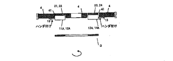
従来の磁気式エンコーダとしては、図8の検出機構部と図10に示す検出回路を組み合わせて構成されているものがある。(例えば、特許文献1参照)。
図8は、1回転あたり1パルスの矩形波信号で、かつ、回転方向を検出するため90度位相差の2信号が得られる磁気式検出装置の検出機構部の斜視図を示す。プリント基板4の表面にバイアス磁石2を固定し、プリント基板4の裏面に磁気抵抗素子11,12,13,14(点線にて表示)を固定している。移動磁石3は、磁気抵抗素子11,12,13,14に対向して回転する。図9は各部品の取り付け位置関係を示した断面図である。15は、磁気抵抗素子11,12,13,14のリード部である。図9において、移動磁石3と磁気抵抗素子11,12,13,14は、所定のギャップをもって対向しており、4個の磁気抵抗素子のリード部15は、プリント基板4にハンダ付けで固定されている。プリント基板4を挟んだ反対面には、環状のバイアス磁石2が固定してある。環状のバイアス磁石2は、磁気抵抗素子11,12,13,14に必要なバイアス磁界を与えることにより、図10に示す検出回路7で1回転に1パルスの矩形波信号72,73を得る。1パルスの矩形波信号72,73は、お互いの矩形波信号が電気的に90度位相差を持ち、この位相差を検出することにより回転方向を検出する。
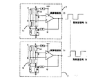
図10は、検出回路7の回路構成を示す。移動磁石3が回転することにより発生する磁界の変化を、対向した4個の磁気抵抗素子11,12,13,14で検出し、検出回路7で矩形波信号72,73を得る。Rは抵抗、VRは可変抵抗を示す。71は、磁気抵抗素子11,12,13,14の信号を矩形波に波形整形するための演算増幅器である。
(Prior art 1)
Some conventional magnetic encoders are configured by combining the detection mechanism shown in FIG. 8 and the detection circuit shown in FIG. (For example, refer to Patent Document 1).
FIG. 8 is a perspective view of a detection mechanism portion of a magnetic detection device that can obtain a rectangular wave signal of one pulse per rotation and two signals having a phase difference of 90 degrees in order to detect the rotation direction. The
FIG. 10 shows a circuit configuration of the detection circuit 7. Changes in the magnetic field generated by the rotation of the moving
図10では検出回路7を2組使用し、回転方向も検出している。磁気抵抗素子の両端に電圧を印加し、移動磁石3の回転によって変化した磁界の変化とバイアス磁石2の磁気変化のベクトル和を磁気抵抗素子で検出し、磁気抵抗素子の中点端子Bに発生する検出信号電圧を演算増幅器71で波形整形して矩形波信号72、73を得る。なお、外部雑音、電圧変動、温度変化に対しての影響を排除する目的で、180度位相差の電気信号が得られる磁気抵抗素子11と磁気抵抗素子13、磁気抵抗素子12と磁気抵抗素子14とを組み合わせ、差信号を波形整形する。
図11は、磁気抵抗素子の内部構成の詳細を示した図である。磁気抵抗素子11,12,13,14は、樹脂で整形された磁気抵抗素子の検出部と磁気抵抗素子のリード部にて構成される。磁気抵抗素子本体は、2組の櫛形状磁気抵抗パターンで構成されたチップ10を使用し、C1は、チップ10の中心を示す。A,B,Cは、磁気抵抗素子のリード部の端子番号名で、端子Bより検出信号が出力される。
In FIG. 10, two sets of detection circuits 7 are used to detect the rotation direction. A voltage is applied to both ends of the magnetoresistive element, and the vector sum of the magnetic field change caused by the rotation of the moving
FIG. 11 is a diagram showing details of the internal configuration of the magnetoresistive element. The
図12は、磁気抵抗素子11,12,13,14と環状のバイアス磁石2の位置関係を示す。磁気抵抗素子の検出部のチップ10の中心C1と環状のバイアス磁石2のN極とS極の境界部が一致するように位置決めしてある。環状のバイアス磁石2は、プリント基板4を挟んだ反対面に磁気抵抗素子11,12,13,14と同一の円周上に固定してある。図13は移動磁石3のN極とS極の磁極構成を示した平面図である。磁気抵抗素子は、N極とS極の磁気境界部で磁気変化を検出するため、バイアス磁石を使用しないと1回転に2パルスの矩形波信号を検出する。そこで、1回転に1パルスを得るために、図13に示した回転側の移動磁石3の磁極構成と図12に示した固定側のバイアス磁石2の磁極構成を採用し、この組み合わせによる磁気変化のベクトル和を磁気抵抗素子で検出し、1回転に1パルスの矩形波信号72,73を得る。
FIG. 12 shows the positional relationship between the
(従来技術2)
また、特許文献1には上記装置の改良技術として図4、図5の検出機構部と図10の従来技術1と同一の検出回路で構成されたものが開示されている。図4は磁気抵抗素子とバイアス磁石の取り付け構成を示す検出機構部の斜視図である。磁気抵抗素子をプリント基板4に取り付け、従来技術1で示したバイアス磁石2を分割したバイアス磁石21,22,23,24をそれぞれ磁気抵抗素子の検出部11A,12A,13A,14Aの上に固定している。図5は各部品の位置関係を示した断面図である。プリント基板4に磁気抵抗素子の検出部11A,12A,13A,14Aと、バイアス磁石21,22,23,24を同時に取り付けるための位置決め部41(プリント基板4にあけられた穴部)を4カ所配設し、そこに磁気抵抗素子の検出部11A,12A,13A,14Aとバイアス磁石21,22,23,24を取り付けている。
環状の移動磁石3と磁気抵抗素子は対向しており、4個の磁気抵抗素子の検出部11A,12A,13A,14Aをプリント基板4の位置決め部41に挿入し、磁気抵抗素子の各リード部15は、プリント基板4にハンダ付けにて固定している。磁気抵抗素子と移動磁石3の関係および構成は、従来技術1と同一である。バイアス磁石21,22,23,24の形状寸法は、磁気抵抗素子の検出部11A,12A,13A,14Aの形状寸法と同一である。
プリント基板4の位置決め部41に磁気抵抗素子の検出部11A,12A,13A,14Aを挿入して、磁気抵抗素子の各リード部15をハンダ付けにより固定し、その後磁気抵抗素子の検出部11A,12A,13A,14Aの裏面に接着剤を塗布し、位置決め部41を利用してバイアス磁石21,22,23,24を接着固定すればバイアス磁石の取り付けは完了する。バイアス磁石21,22,23,24のN極とS極の磁極境界線と磁気抵抗素子11,12,13,14の中点部C1とが一致するようにバイアス磁石21,22,23,24が予め着磁されており、機械的な位置決めのみで磁気抵抗素子にバイアス磁界を与えることができる。位置決め部41の寸法は、磁気抵抗素子の検出部11A,12A,13A,14Aの形状寸法およびバイアス磁石21,22,23,24の形状寸法とほぼ同一で、磁気抵抗素子の検出部11A,12A,13A,14Aとバイアス磁石21,22,23,24がなめらかに挿入できる寸法としている。
(Prior art 2)
Further, Patent Document 1 discloses an improvement technique of the above-described device, which is configured by the detection mechanism section shown in FIGS. 4 and 5 and the same detection circuit as that of the conventional technique 1 shown in FIG. FIG. 4 is a perspective view of a detection mechanism portion showing a configuration for attaching a magnetoresistive element and a bias magnet. A magnetoresistive element is attached to the printed circuit board 4, and the
The annular moving
The magnetoresistive
図6はプリント基板4の位置決め部41の形状の詳細を示した図である。磁気抵抗素子の検出部11A,12A,13A,14Aとバイアス磁石21,22,23,24の位置決め部品としてプリント基板4に設けた位置決め部41(プリント基板4にあけられた穴部)を使用している。
図7は磁気抵抗素子11,12,13,14とバイアス磁石21,22,23,24の取り付けの関係を示した図である。バイアス磁石21,22,23,24のN極とS極の磁極境界線が、プリント基板4の裏面にある磁気抵抗素子11,12,13,14(リード部のみ点線で表示)の中点部C1に一致するように配置されている。
FIG. 7 is a diagram showing the attachment relationship between the
ところが、従来技術1では、環状のバイアス磁石2を磁気抵抗素子取付のプリント基板4の反対面に、磁気抵抗素子と同一円周上で、かつ磁気抵抗素子のチップ10の中心C1と一致するように位置決めして固定することが必要であるが、これには環状のバイアス磁石2には円周方向の位置決め機能がない。しかも、環状のバイアス磁石2の磁極位置が目視では見えないため、位置決め治具(図示せず。)によって取り付ける必要があった。さらに、環状のバイアス磁石2のため、磁気抵抗素子11,12,13,14が配置されていないプリント基板4の反対面の同一円周上にも他の部品が実装できず、部品実装密度が低下し、プリント基板外形寸法が大きくなって磁気式エンコーダが小形化できないという問題があった。
また、従来技術2では、磁気抵抗素子とバイアス磁石2を位置決め冶具を使用しないで同時に位置決めできるが、このためにリード端子タイプの磁気抵抗素子の外形よりやや大きな穴の位置決め部を設けたため、表面実装タイプの磁気抵抗素子を用いることができず小形化が困難であった。
また、プリント基板に配設される位置決め部(プリント基板4にあけられた穴部)の大きさはリード端子タイプ磁気抵抗素子の検出部モールドの外形により決まるため、本来必要なバイアス磁石サイズが小さくても磁気抵抗素子の外形に合わせて配設、穿孔する必要があり、必要以上の穿孔部分によってプリント基板の強度を低下させる上、パターン配線の自由度を低下させるという問題があった。
そこで、本発明は位置決め冶具を使用せずバイアス磁石2を取り付けるとともに、表面実装タイプの磁気抵抗素子を用い、これによりプリント基板の部品実装密度を向上させることができ、品質の向上と小形化が可能な磁気式エンコーダを提供することを目的とする。
However, in the prior art 1, the
In the
In addition, since the size of the positioning portion (hole formed in the printed circuit board 4) arranged on the printed circuit board is determined by the outer shape of the detection part mold of the lead terminal type magnetoresistive element, the originally required bias magnet size is small. However, it is necessary to arrange and perforate according to the outer shape of the magnetoresistive element, and there is a problem that the strength of the printed circuit board is reduced by the perforated part more than necessary, and the degree of freedom of the pattern wiring is lowered.
Therefore, the present invention attaches the
上記問題を解決するため、本発明は、次のように構成したものである。
すなわち、本発明の一の観点による磁気式エンコーダは、磁気抵抗素子と、前記磁気抵抗素子にバイアス磁界を与えるバイアス磁石と、前記磁気抵抗素子に対して対向し、相対移動する移動磁石と、前記磁気抵抗素子を取り付けるための取り付け部品と、を備え、前記取り付け部品は、前記バイアス磁石を位置決めするための位置決め部を有し、前記位置決め部の外形寸法は、前記磁気抵抗素子の外形寸法より小さいことを特徴とする。
また、上記一の観点による磁気式エンコーダは、前記取り付け部品がプリント基板であり、前記位置決め部がプリント基板にあけられた貫通穴部であることを特徴とする。
また、上記一の観点による磁気式エンコーダは、磁気抵抗素子が表面実装タイプの磁気抵抗素子であることを特徴としてもよい。
また、上記一の観点による磁気式エンコーダは、前記位置決め部が、前記磁気抵抗素子の実装領域で電極用パッドに囲まれた領域に配設されていることを特徴としてもよい。
また、上記一の観点による磁気式エンコーダは、前記プリント基板に設けた貫通穴部は全体が角形をなし、かつ四隅には前記バイアス磁石挿入時のバイアス磁石のカケ防止のための半円形の抜き穴を有することを特徴としてもよい。
また、上記一の観点による磁気式エンコーダは、前記バイアス磁石に磁極のN極とS極の境界を表すケガキ線とN極またはS極の極性を表す印をつけたことを特徴としてもよい。
また、本発明の他の観点によれば、上記一の観点による磁気式エンコーダのバイアス磁石の取り付け方法において、プリント基板のパッドにあわせて磁気抵抗素子を実装して、その後磁気抵抗素子の検出部裏面に接着剤を塗布し、前記貫通穴部を利用してバイアス磁石を接着固定することを特徴とする。
また、本発明の更に他の観点によるサーボモータは、上記一の観点による磁気式エンコーダを搭載したことを特徴とする。
In order to solve the above problems, the present invention is configured as follows.
That is, a magnetic encoder according to an aspect of the present invention includes a magnetoresistive element, a bias magnet that applies a bias magnetic field to the magnetoresistive element, a moving magnet that faces the magnetoresistive element and moves relative to the magnetoresistive element, An attachment part for attaching the magnetoresistive element, and the attachment part has a positioning part for positioning the bias magnet, and an outer dimension of the positioning part is smaller than an outer dimension of the magnetoresistive element. and wherein the decoction.
The magnetic encoder according to the perspective of the one, the mounting part is a printed circuit board, and wherein the pre-Symbol position-decided Me portion is a through hole drilled in the printed circuit board.
In the magnetic encoder according to the first aspect, the magnetoresistive element may be a surface mount type magnetoresistive element.
The magnetic encoder according to the perspective of the one of the previous SL-position-decided Me section may be characterized in that it is arranged in the surrounded by the electrode pads in the mounting region of the magnetoresistive element region.
In the magnetic encoder according to the first aspect, the through hole provided in the printed circuit board has a square shape as a whole, and the four corners are semicircular holes for preventing the bias magnet from being broken when the bias magnet is inserted. It may be characterized by having a hole.
The magnetic encoder according to the first aspect may be characterized in that the bias magnet is marked with a marking line indicating the boundary between the north pole and the south pole of the magnetic pole and the polarity of the north pole or the south pole.
According to another aspect of the present invention, in the method for attaching a bias magnet of the magnetic encoder according to the above aspect, the magnetoresistive element is mounted in accordance with the pad of the printed circuit board, and then the magnetoresistive element detection unit An adhesive is applied to the back surface, and the bias magnet is bonded and fixed using the through hole.
A servo motor according to still another aspect of the present invention is characterized in that the magnetic encoder according to the above aspect is mounted.
以上述べたように、本発明によれば、磁気抵抗素子を取り付けるための取り付け部品には、磁気抵抗素子とバイアス磁石を位置決めするための位置決め部を磁気抵抗素子より小さい寸法で配設したことにより、従来の位置決め冶具による取り付けが不要となり、取り付けが容易になり、その分取り付け時間を短縮することができる。また、今まで環状のバイアス磁石により実装ができなかったプリント基板部に他の部品を実装でき、プリント基板の部品実装率が向上する結果、プリント基板の外形寸法が小さくなり、磁気式エンコーダが小形になるという効果がある。また、プリント基板4に磁気抵抗素子を実装する反対側の実装部品を効率よく取り付けることができ、さらに、プリント基板4内のパターン配線の自由度が増し効率よく配線ができるうえ、位置決め部41の貫通穴部が、プリント基板4の中心の穴部にかかることが無くなるので、プリント基板4の強度が向上する。さらに、バイアス磁石の片面に磁極のN極とS極の磁極境界を示すケガキ線と極性を表す印を付けてバイアス磁石を固定することにより、バイアス磁石の取り付けミスがなくなり、品質が向上するという効果が発生する。
As described above, according to the present invention, the mounting part for mounting the magnetoresistive element is provided with the positioning portion for positioning the magnetoresistive element and the bias magnet with a smaller size than the magnetoresistive element. Thus, the attachment with the conventional positioning jig becomes unnecessary, the attachment becomes easy, and the attachment time can be shortened accordingly. In addition, other parts can be mounted on the printed circuit board part that could not be mounted with an annular bias magnet until now, and the component mounting rate of the printed circuit board is improved. As a result, the external dimensions of the printed circuit board are reduced, and the magnetic encoder is smaller. There is an effect of becoming. Further, the mounting component on the opposite side on which the magnetoresistive element is mounted can be efficiently attached to the printed circuit board 4, the degree of freedom of pattern wiring in the printed circuit board 4 is increased, and the wiring can be performed efficiently. Since the through hole does not cover the central hole of the printed circuit board 4, the strength of the printed circuit board 4 is improved. Furthermore, fixing the bias magnet with a marking indicating the magnetic pole boundary between the N pole and the S pole of the magnetic pole on one side of the bias magnet and fixing the bias magnet eliminates the mistake in attaching the bias magnet and improves the quality. An effect occurs.
以下、本発明の実施例を図に基づいて説明する。 Embodiments of the present invention will be described below with reference to the drawings.
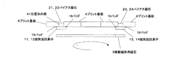
図1は、本発明の磁気抵抗素子とバイアス磁石の取り付け構成の第1の実施例を示す検出機構部の上面図である。本実施例の磁気式エンコーダは、図1の検出機構部と図10の従来例と同一の検出回路で構成される。磁気抵抗素子11,12,13,14を取り付けるための取り付け部品としてプリント基板4を使用している。バイアス磁石21,22,23,24をそれぞれ磁気抵抗素子の検出部の上に固定する。図2は、実施例の各部品の位置関係を示した断面図である。プリント基板4には磁気抵抗素子11,12,13,14を固定するためのパッド16と磁気抵抗素子実装後バイアス磁石21,22,23,24を取り付けるための位置決め部41(プリント基板4にあけられた貫通穴部)が4カ所配設されており、この位置決め部を用いて磁気抵抗素子11,12,13,14とバイアス磁石21,22,23,24を取り付ける。
FIG. 1 is a top view of a detection mechanism portion showing a first embodiment of a mounting configuration of a magnetoresistive element and a bias magnet according to the present invention. The magnetic encoder of the present embodiment is constituted by the detection mechanism section of FIG. 1 and the same detection circuit as the conventional example of FIG. The printed circuit board 4 is used as an attachment part for attaching the
環状の移動磁石3と磁気抵抗素子11,12,13,14は対向しており、4個の磁気抵抗素子をプリント基板4のパッド16上に実装している。磁気抵抗素子11,12,13,14と移動磁石3の関係および構成は、従来例と同一である。
本発明が従来技術と異なるのは、磁気抵抗素子として表面実装タイプのものを使い、バイアス磁石とバイアス磁石を取り付けるための位置決め部(プリント基板4にあけられた穴部)を磁気抵抗素子より小さく構成したことにある。
The annular moving
The present invention is different from the prior art in that a surface mount type magnetoresistive element is used, and a positioning portion (a hole formed in the printed circuit board 4) for attaching the bias magnet is made smaller than the magnetoresistive element. It is in the configuration.
プリント基板4に磁気抵抗素子11,12,13,14をパッド16にあわせ実装して、その後、磁気抵抗素子の検出部11,12,13,14の裏面に接着剤を塗布し、位置決め部41を利用してバイアス磁石21,22,23,24を接着固定すればバイアス磁石の取り付けは完了する。バイアス磁石21,22,23,24のN極とS極の磁極境界線と磁気抵抗素子11,12,13,14の中点部C1とが一致するようにバイアス磁界用磁石21,22,23,24が予め着磁されているので、機械的な位置決めのみで磁気抵抗素子11,12,13,14に適切なバイアス磁界を与えることができる。位置決め部41の寸法は、磁気抵抗素子11,12,13,14の形状寸法より小さく、バイアス磁石21,22,23,24がなめらかに挿入できる寸法としている。
The
バイアス磁石21,22,23,24を磁気抵抗素子11,12,13,14より小さい寸法にした結果、環状のバイアス磁石2がなくなり、且つ、プリント基板4に磁気抵抗素子を実装する反対側の実装部品を効率よく取り付けることができ、さらに、プリント基板4内のパターン配線の自由度が増し効率よく配線ができる上、位置決め部41の貫通穴部が、プリント基板4の中心の穴部にかかることが無くなるので、プリント基板4の強度が向上する。
As a result of making the
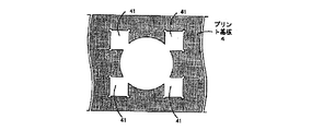
図3は位置決め部41とバイアス磁石の様子を拡大表示した図である。位置決め部41である貫通穴部は全体が角形をなし、4隅には半円形の抜き穴42が設けられている。この抜き穴42はバイアス磁石装着時にプリント基板4とバイアス磁石21,22,23,24をぶつけることによって生じるカケなどを防止するためのものである。
バイアス磁石21,22,23,24の外形形状が矩形で磁気抵抗素子11,12,13,14上に取り付ける場合、着磁状態が目視で判別できないため、取り付けミスをする可能性がある。そこで、図3にしめすようにバイアス磁石21,22,23,24磁石の片面に磁極のN極とS極の境界にケガキ線44とまた磁極のたとえばS(N)極を表す印を付けるようにしている。このことから境界および極性が明確になり、確実にバイアス磁石21,22,23,24を取り付けることができる。
なお、本発明の実施例として特に図示していないが、本発明による磁気式エンコーダをサーボモータの位置検出装置として搭載する場合にも同じ効果が得られることはいうまでもない。
FIG. 3 is an enlarged view of the
When the outer shape of the
Although not specifically shown as an embodiment of the present invention, it is needless to say that the same effect can be obtained when the magnetic encoder according to the present invention is mounted as a position detection device for a servo motor.
10 チップ
11,12,13,14 磁気低抗素子
11A,12A,13A,14A 磁気低抗素子の検出部
15リード部
16パッド
C1 磁気抵抗素子中点部
2,21,22,23,24バイアス磁石
3 移動磁石
4 プリント基板(取り付け部品)
41 位置決め部
42 抜き穴
43 S(N)極性表示印
44 N−S極境界表示ケガキ線
7 検出回路
71 演算増幅器
72,73 矩形波信号
10
41 Positioning portion 42 Punching hole 43 S (N) polarity display mark 44 NS pole boundary display marking line 7 Detection circuit 71 Operational amplifiers 72 and 73 Rectangular wave signal
Claims (8)
前記磁気抵抗素子にバイアス磁界を与えるバイアス磁石と、
前記磁気抵抗素子に対して対向し、相対移動する移動磁石と、
前記磁気抵抗素子を取り付けるための取り付け部品と、
を備え、
前記取り付け部品は、前記バイアス磁石を位置決めするための位置決め部を有し、
前記位置決め部の外形寸法は、前記磁気抵抗素子の外形寸法より小さい、磁気式エンコーダ。 A magnetoresistive element;
A bias magnet for applying a bias magnetic field to the magnetoresistive element;
A moving magnet facing and relatively moving with respect to the magnetoresistive element;
A mounting part for mounting the magnetoresistive element;
With
The mounting part has a positioning part for positioning the bias magnet,
Dimensions of the positioning portion is not smaller than the outer dimension of the magnetoresistive element, magnetic encoder.
前記位置決め部が、前記プリント基板にあけられた貫通穴部である、請求項1に記載の磁気式エンコーダ。 The mounting component is a printed circuit board;
The magnetic encoder according to claim 1, wherein the positioning portion is a through hole portion formed in the printed circuit board.
前記プリント基板のパッドにあわせて前記磁気抵抗素子を実装し、
その後前記磁気抵抗素子の検出部裏面に接着剤を塗布して、前記貫通穴部を利用してバイアス磁石を接着固定する、磁気式エンコーダのバイアス磁石取り付け方法。 The method of attaching a bias magnet of a magnetic encoder according to claim 4,
Mount the magnetoresistive element according to the pad of the printed circuit board,
A method of attaching a bias magnet to a magnetic encoder, wherein an adhesive is applied to the back surface of the detection portion of the magnetoresistive element, and a bias magnet is bonded and fixed using the through hole.
A servo motor on which the magnetic encoder according to claim 1 is mounted.
Priority Applications (1)
| Application Number | Priority Date | Filing Date | Title |
|---|---|---|---|
| JP2008016176A JP5240429B2 (en) | 2008-01-28 | 2008-01-28 | Magnetic encoder |
Applications Claiming Priority (1)
| Application Number | Priority Date | Filing Date | Title |
|---|---|---|---|
| JP2008016176A JP5240429B2 (en) | 2008-01-28 | 2008-01-28 | Magnetic encoder |
Publications (3)
| Publication Number | Publication Date |
|---|---|
| JP2009175073A JP2009175073A (en) | 2009-08-06 |
| JP2009175073A5 JP2009175073A5 (en) | 2011-10-20 |
| JP5240429B2 true JP5240429B2 (en) | 2013-07-17 |
Family
ID=41030313
Family Applications (1)
| Application Number | Title | Priority Date | Filing Date |
|---|---|---|---|
| JP2008016176A Active JP5240429B2 (en) | 2008-01-28 | 2008-01-28 | Magnetic encoder |
Country Status (1)
| Country | Link |
|---|---|
| JP (1) | JP5240429B2 (en) |
Families Citing this family (4)
| Publication number | Priority date | Publication date | Assignee | Title |
|---|---|---|---|---|
| US9574906B2 (en) * | 2013-10-28 | 2017-02-21 | Hitachi Metals, Ltd. | Magnetic medium for magnetic encoder, magnetic encoder and method for manufacturing magnetic medium |
| US20170016745A1 (en) * | 2014-03-24 | 2017-01-19 | Panasonic Intellectual Property Management Co., Ltd. | Magnetic sensor |
| US10094890B2 (en) | 2014-10-09 | 2018-10-09 | Panasonic Intellectual Property Management Co., Ltd. | Magnetic sensor |
| JP2017150956A (en) * | 2016-02-25 | 2017-08-31 | アルプス電気株式会社 | Position detector |
Family Cites Families (2)
| Publication number | Priority date | Publication date | Assignee | Title |
|---|---|---|---|---|
| JPH05119137A (en) * | 1991-01-29 | 1993-05-18 | Matsushita Electric Ind Co Ltd | Ferromagnetic thin-film resistance element |
| JP3941082B2 (en) * | 1998-01-28 | 2007-07-04 | 株式会社安川電機 | Magnetic detector |
-
2008
- 2008-01-28 JP JP2008016176A patent/JP5240429B2/en active Active
Also Published As
| Publication number | Publication date |
|---|---|
| JP2009175073A (en) | 2009-08-06 |
Similar Documents
| Publication | Publication Date | Title |
|---|---|---|
| JP3941082B2 (en) | Magnetic detector | |
| KR100595078B1 (en) | Magnetic detecting device | |
| JP5666886B2 (en) | Rotary encoder | |
| WO2007102465A1 (en) | Magnetic sensor device, magnetic encoder device, and magnetic scale manufacturing method | |
| JP5240429B2 (en) | Magnetic encoder | |
| JP2007271608A (en) | Magnetometric sensor device and magnetic encoder device | |
| JP3487452B2 (en) | Magnetic detector | |
| JPH07264833A (en) | Motor | |
| US6417587B1 (en) | Motor | |
| JP5006671B2 (en) | Magnetic encoder | |
| JP5651040B2 (en) | Sensor unit and composite substrate | |
| JP4967852B2 (en) | Magnetic encoder and motor | |
| JP5651039B2 (en) | Rotary encoder | |
| JP2009175073A5 (en) | ||
| JP2002131406A (en) | Magnetism detector | |
| JP2003004484A (en) | Rotation sensor | |
| JP5651038B2 (en) | Rotary encoder | |
| JP3269307B2 (en) | Pickup sensor and vehicle speed detection device using pickup sensor | |
| JP4154524B2 (en) | Rotary magnetic sensor | |
| JP7394570B2 (en) | brushless motor | |
| JP5083130B2 (en) | Mounting method of rotation detector | |
| JP7026517B2 (en) | Magnetic linear encoder | |
| JPH08201016A (en) | Angle of rotation detector | |
| JP2005147970A (en) | Rotation-detecting device | |
| JPH09318389A (en) | Magnetic detector |
Legal Events
| Date | Code | Title | Description |
|---|---|---|---|
| A621 | Written request for application examination |
Free format text: JAPANESE INTERMEDIATE CODE: A621 Effective date: 20101117 |
|
| A521 | Written amendment |
Free format text: JAPANESE INTERMEDIATE CODE: A523 Effective date: 20110906 |
|
| RD02 | Notification of acceptance of power of attorney |
Free format text: JAPANESE INTERMEDIATE CODE: A7422 Effective date: 20120306 |
|
| A131 | Notification of reasons for refusal |
Free format text: JAPANESE INTERMEDIATE CODE: A131 Effective date: 20121003 |
|
| A521 | Written amendment |
Free format text: JAPANESE INTERMEDIATE CODE: A523 Effective date: 20121130 |
|
| TRDD | Decision of grant or rejection written | ||
| A01 | Written decision to grant a patent or to grant a registration (utility model) |
Free format text: JAPANESE INTERMEDIATE CODE: A01 Effective date: 20130306 |
|
| A61 | First payment of annual fees (during grant procedure) |
Free format text: JAPANESE INTERMEDIATE CODE: A61 Effective date: 20130319 |
|
| FPAY | Renewal fee payment (event date is renewal date of database) |
Free format text: PAYMENT UNTIL: 20160412 Year of fee payment: 3 |
|
| R150 | Certificate of patent or registration of utility model |
Free format text: JAPANESE INTERMEDIATE CODE: R150 Ref document number: 5240429 Country of ref document: JP Free format text: JAPANESE INTERMEDIATE CODE: R150 |