JP5228331B2 - Optical scanning apparatus, image forming apparatus, and multicolor image forming apparatus - Google Patents
Optical scanning apparatus, image forming apparatus, and multicolor image forming apparatus Download PDFInfo
- Publication number
- JP5228331B2 JP5228331B2 JP2007031947A JP2007031947A JP5228331B2 JP 5228331 B2 JP5228331 B2 JP 5228331B2 JP 2007031947 A JP2007031947 A JP 2007031947A JP 2007031947 A JP2007031947 A JP 2007031947A JP 5228331 B2 JP5228331 B2 JP 5228331B2
- Authority
- JP
- Japan
- Prior art keywords
- optical
- scanning device
- scanning
- optical scanning
- light source
- Prior art date
- Legal status (The legal status is an assumption and is not a legal conclusion. Google has not performed a legal analysis and makes no representation as to the accuracy of the status listed.)
- Expired - Fee Related
Links
Images


Classifications
-
- G—PHYSICS
- G02—OPTICS
- G02B—OPTICAL ELEMENTS, SYSTEMS OR APPARATUS
- G02B26/00—Optical devices or arrangements for the control of light using movable or deformable optical elements
- G02B26/08—Optical devices or arrangements for the control of light using movable or deformable optical elements for controlling the direction of light
- G02B26/10—Scanning systems
- G02B26/105—Scanning systems with one or more pivoting mirrors or galvano-mirrors
-
- B—PERFORMING OPERATIONS; TRANSPORTING
- B41—PRINTING; LINING MACHINES; TYPEWRITERS; STAMPS
- B41J—TYPEWRITERS; SELECTIVE PRINTING MECHANISMS, i.e. MECHANISMS PRINTING OTHERWISE THAN FROM A FORME; CORRECTION OF TYPOGRAPHICAL ERRORS
- B41J2/00—Typewriters or selective printing mechanisms characterised by the printing or marking process for which they are designed
- B41J2/435—Typewriters or selective printing mechanisms characterised by the printing or marking process for which they are designed characterised by selective application of radiation to a printing material or impression-transfer material
- B41J2/47—Typewriters or selective printing mechanisms characterised by the printing or marking process for which they are designed characterised by selective application of radiation to a printing material or impression-transfer material using the combination of scanning and modulation of light
- B41J2/471—Typewriters or selective printing mechanisms characterised by the printing or marking process for which they are designed characterised by selective application of radiation to a printing material or impression-transfer material using the combination of scanning and modulation of light using dot sequential main scanning by means of a light deflector, e.g. a rotating polygonal mirror
-
- G—PHYSICS
- G02—OPTICS
- G02B—OPTICAL ELEMENTS, SYSTEMS OR APPARATUS
- G02B3/00—Simple or compound lenses
- G02B3/12—Fluid-filled or evacuated lenses
- G02B3/14—Fluid-filled or evacuated lenses of variable focal length
Description
本発明は、電子写真方式の画像形成装置に用いられる光走査装置や、光走査型のバーコード読み取り装置、車載用のレーザレーダ装置などへも応用が可能な光走査装置に関し、さらには、その光走査装置を用いたデジタル複写機、レーザプリンタ、レーザプロッタ、レーザファクシミリ、あるいはこれらの複合機などの画像形成装置に関する。 The present invention relates to an optical scanning device that can be applied to an optical scanning device used in an electrophotographic image forming apparatus, an optical scanning barcode reader, an in-vehicle laser radar device, and the like. The present invention relates to an image forming apparatus such as a digital copying machine, a laser printer, a laser plotter, a laser facsimile, or a composite machine using these optical scanning devices.
従来の光走査装置においては、光ビームを走査する偏向器としてポリゴンミラーやガルバノミラーが用いられているが、より高解像度な画像と高速プリントを達成するにはこの回転をさらに高速にしなければならず、軸受の耐久性や風損による発熱、騒音が課題となり、高速走査に限界がある。 In a conventional optical scanning device, a polygon mirror or a galvanometer mirror is used as a deflector for scanning a light beam. However, in order to achieve a higher resolution image and high-speed printing, this rotation must be further increased. However, the durability of the bearing, heat generation due to windage damage, and noise become problems, and there is a limit to high-speed scanning.
これに対して、近年シリコンマイクロマシニングを利用した偏向装置の研究が進められており、例えば特許文献1(特許第2924200号公報)や特許文献2(特許第3011144号公報)に開示されているようにSi基板で振動ミラーとそれを軸支するねじり梁を一体形成した方式が提案されている。
この方式によれば、ミラー面サイズが小さく小型化できるうえ、共振を利用して往復振動させるので高速動作が可能であるにもかかわらず、低騒音で消費電力が低いという利点がある。さらに、低振動で、発熱がほとんどないために、光走査装置を収容するハウジングを薄肉化でき、ガラス繊維の配合率が少ない低コストな樹脂成形材を用いても画像品質への影響が発生し難いといった利点もある。
On the other hand, research on a deflection apparatus using silicon micromachining has recently been advanced, and for example, it is disclosed in Patent Document 1 (Patent No. 2924200) and Patent Document 2 (Patent No. 3101144). In addition, there is proposed a method in which a vibrating mirror and a torsion beam that pivotally supports it are integrally formed on a Si substrate.
According to this method, there is an advantage that the mirror surface size can be reduced and the size can be reduced, and since reciprocal vibration is performed using resonance, high speed operation is possible but low noise and low power consumption are possible. Furthermore, since the vibration is low and there is almost no heat generation, the housing that houses the optical scanning device can be thinned, and even if a low-cost resin molding material with a low glass fiber content is used, the image quality is affected. There is also an advantage that it is difficult.
特許文献3(特開2004−279947号公報)には、ポリゴンミラーの代わりに振動ミラーを配備した光走査装置の例が開示されている。
しかし、正弦波振動を行うマイクロミラーを偏向手段に用いると、偏向角度が正弦波的に変化するので、走査結像光学系に現状の書込光学系に用いられているfθレンズを用いた場合、周辺像高において走査速度が遅くなり、被走査面上での走査速度が等速ではなくなる。走査速度の等速性が悪いと、主走査方向周辺で画像の歪等が発生し、画像品質の劣化を引き起こすという問題点がある。また、電気的に等速性を補正する内容も同時に開示されているが、この場合、補正量の段差が大きいと、階段状にドット間隔の疎密を発生させるため濃度が変化してしまい画像が劣化するので、電気的補正量には限界がある。隣接領域で段差が急峻だと、濃度差として検知できてしまうことが官能評価より明らかになっており、自ずとその補正限界量も決まってくる。正弦波的に振動する振動ミラーとfθレンズを用いた場合は、等速走査を行うための必要補正量がこの限界補正量を超えており、電気的な補正では補正しきれない。
Patent Document 3 (Japanese Patent Application Laid-Open No. 2004-279947) discloses an example of an optical scanning device in which a vibrating mirror is provided instead of a polygon mirror.
However, if a micromirror that performs sinusoidal vibration is used as a deflecting means, the deflection angle changes sinusoidally, so that the fθ lens used in the current writing optical system is used as the scanning imaging optical system. The scanning speed becomes slow at the peripheral image height, and the scanning speed on the scanned surface is not constant. If the scanning speed is not uniform, there is a problem in that image distortion or the like occurs in the vicinity of the main scanning direction, causing deterioration in image quality. In addition, contents for electrically correcting the constant velocity are disclosed at the same time, but in this case, if the level difference of the correction amount is large, the density is changed because the density of the dot interval is changed stepwise, and the image is changed. Since it deteriorates, there is a limit to the amount of electrical correction. It is clear from sensory evaluation that if the step is steep in the adjacent region, it can be detected as a density difference, and the correction limit amount is determined naturally. When a oscillating mirror that vibrates sinusoidally and an fθ lens are used, the necessary correction amount for performing constant-speed scanning exceeds the limit correction amount and cannot be corrected by electrical correction.
この問題に対して、特許文献4(特開2005−215571号公報)においては、次式、
H=K×sin-1(θ/2θmax)
但し、H:像高、K:比例定数、θ:振れ角、θmax:振幅(最大振れ角)
で示されるような結像特性(f・arcsin特性)を有する走査結像光学系を用いることにより、主走査光束のウェスト位置を光学的に補正し、広い有効書込幅と、良好な走査等速性を有する光走査装置を得ることが記載されている。
しかし、走査結像光学系にて光学的補正を行うと、像高によって形状や屈折力が変化する走査結像光学素子に、像高によって異なる角度で、かつ、異なる位置に入射するので、特に周辺像高において結像光学素子上にて光線の波面の劣化が生じ、波動光学的収差の影響によりビームスポット径の劣化、ひいては画像品質の劣化を招くという問題点があった。また、被走査面上において主走査光束のスポット径の像高間偏差が大きくなり、画像品質の劣化を招くという問題点があった。
With respect to this problem, in Patent Document 4 (Japanese Patent Laid-Open No. 2005-215571), the following equation:
H = K × sin −1 (θ / 2θ max )
Where H: image height, K: proportionality constant, θ: shake angle, θ max : amplitude (maximum shake angle)
By using a scanning imaging optical system having imaging characteristics (f · arcsin characteristics) as shown in Fig. 4, the waist position of the main scanning light beam is optically corrected, a wide effective writing width, good scanning, etc. It is described that an optical scanning device having speed is obtained.
However, when optical correction is performed by the scanning imaging optical system, it enters the scanning imaging optical element whose shape and refractive power change depending on the image height at different angles and at different positions. At the peripheral image height, the wavefront of the light beam is deteriorated on the imaging optical element, and the beam spot diameter is deteriorated due to the influence of the wave optical aberration, and the image quality is deteriorated. In addition, there is a problem in that the image height deviation of the spot diameter of the main scanning light beam increases on the surface to be scanned, leading to deterioration of image quality.
また、特許文献5(特開平8−286135号公報)には、光源、もしくはカップリングレンズ、及びシリンドリカルレンズの位置を光軸方向に調整する機構を設けて、感光体表面のビームスポット径を補正する例が開示されているが、光学素子の位置を調整する機構を2つ以上も備えており、システムとして安定性に欠ける点や、調整機構を有していても、fθ光学系の走査結像光学系が必要である点、また、ポリゴンミラーを用いており、発熱、振動、騒音、消費電力などにおいて振動ミラーに劣るという点が問題であった。 Patent Document 5 (JP-A-8-286135) corrects the beam spot diameter on the surface of the photoreceptor by providing a mechanism for adjusting the position of the light source, coupling lens, and cylindrical lens in the optical axis direction. Although there are two or more mechanisms for adjusting the position of the optical element, the system lacks stability, and even if it has an adjustment mechanism, the scan connection of the fθ optical system is disclosed. There are problems in that an image optical system is necessary, and that a polygon mirror is used, and that heat generation, vibration, noise, power consumption, and the like are inferior to a vibration mirror.
本発明は上記事情に鑑みなされたものであり、従来技術の問題点に対し、本発明では、走査等速性を保ちつつ、光線の波面の劣化を生じさせる走査結像光学素子を必要としない構成の光走査装置、及び画像形成装置を構成することにより、光走査装置及び画像形成装置の品質の向上、低コスト化、システムの簡素化、また、安定性の向上を図ることを目的とする。
また、本発明は、振動ミラーをポリゴンミラーの代わりとして用いることで、低騒音化や低消費電力化を可能し、オフィス環境に適合した画像形成装置を提供することを目的とする。
さらに本発明は、振動ミラーを用いることによる低消費電力化で、地球環境にも適合した画像形成装置を提供することを目的とする。
さらにまた本発明は、低振動化、低発熱化に伴ってハウジングが薄肉化でき、軽量化や低コスト化を可能として光走査装置及び画像形成装置を提供することを目的とする。
The present invention has been made in view of the above circumstances, and in contrast to the problems of the prior art, the present invention does not require a scanning imaging optical element that causes deterioration of the wavefront of a light beam while maintaining scanning constant velocity. It is an object of the present invention to improve the quality, lower the cost, simplify the system, and improve the stability of the optical scanning device and the image forming apparatus by configuring the optical scanning device and the image forming apparatus. .
It is another object of the present invention to provide an image forming apparatus that can reduce noise and power consumption by using a vibrating mirror instead of a polygon mirror and is suitable for an office environment.
It is another object of the present invention to provide an image forming apparatus that is low in power consumption by using a vibrating mirror and is suitable for the global environment.
It is a further object of the present invention to provide an optical scanning device and an image forming apparatus that can reduce the thickness of the housing in accordance with the reduction in vibration and heat generation, and can be reduced in weight and cost.
上記の目的を達成するため、本発明では以下のような技術的手段を採っている。
本発明の第1の手段は、光走査装置であって、光源と、該光源を変調する変調クロックを制御する光源駆動手段と、前記光源からの光ビームを走査方向に対して所定の収束状態にする光学素子と、ねじり梁に支持された振動ミラーからなり前記光源からの光ビームを偏向して1つ以上の被走査面を走査する少なくとも一つの光偏向器と、を有する光走査装置において、前記被走査面内の有効走査領域内において、該有効走査領域内の略中央における走査速度に対する各走査位置での走査速度との割合であるリニアリテイが、下記の式1の条件を満足する範囲内となるように、光源クロック周波数およびクロック位相シフト量を制御する前記光源駆動手段と、前記振動ミラーの振れ角と前記有効走査領域に用いる最大振幅を制御する振動ミラー駆動回路を有し、前記光偏向器により前記被走査面に走査される光ビームは、それぞれ被走査面近傍で結像点を有し、該結像点の深度を拡大させる深度拡大手段を有することを特徴とする。
In order to achieve the above object, the present invention employs the following technical means.
The first means of the present invention is an optical scanning device, which is a light source, light source driving means for controlling a modulation clock for modulating the light source, and a light beam from the light source in a predetermined convergence state with respect to the scanning direction. An optical scanning device comprising: an optical element that includes: an oscillating mirror supported by a torsion beam; and at least one optical deflector that deflects a light beam from the light source and scans one or more scanned surfaces. In the effective scanning area in the surface to be scanned, the linearity that is the ratio of the scanning speed at each scanning position to the scanning speed at the approximate center in the effective scanning area satisfies the condition of the following equation (1) so that the inner, oscillating mirror for controlling the light source driving Dote stage for controlling the light source clock frequency and clock phase shift, the maximum amplitude used in the effective scanning area and the deflection angle of the oscillating mirror Has a kinematic circuit, the light beam scanned on the scanning surface by the optical deflector has a imaging point at the surface to be scanned near each have a depth enlarging means for enlarging the depth of said imaging point It is characterized by that.

本発明の第2の手段は、第1の手段の光走査装置において、前記最大偏向角θmaxが22deg近傍であることを特徴とする。
本発明の第3の手段は、第1または2の手段の光走査装置において、前記振動ミラーから前記被走査面へと導かれる光ビームの光路には集光パワーが略0の折り返しミラーのみ配置されていることを特徴とする。
また、本発明の第4の手段は、第1乃至第3のいずれか1つの手段の光走査装置において、前記光源駆動手段によって前記光源の変調クロックを制御することを特徴とする。
According to a second means of the present invention, in the optical scanning device of the first means, the maximum deflection angle θ max is in the vicinity of 22 deg.
According to a third means of the present invention, in the optical scanning device of the first or second means, only a folding mirror having a condensing power of substantially 0 is disposed in the optical path of the light beam guided from the vibrating mirror to the scanned surface. It is characterized by being.
According to a fourth means of the present invention, in the optical scanning device of any one of the first to third means, the light source driving means controls the modulation clock of the light source.
本発明の第5の手段は、第4の手段の光走査装置において、前記光源駆動手段は、前記光偏向器の走査に同期させて、前記変調クロックの周波数を可変することを特徴とする。
また、本発明の第6の手段は、第4の手段の光走査装置において、前記光源駆動手段は、前記光偏向器の走査に同期させて、前記変調クロックの位相を制御することを特徴とする。
さらに本発明の第7の手段は、第4の手段の光走査装置において、前記光源駆動手段は、前記光偏向器の走査に同期させて、前記変調クロックの位相を制御し、かつ、前記変調クロックの周波数を可変することを特徴とする。
According to a fifth means of the present invention, in the optical scanning device of the fourth means, the light source driving means varies the frequency of the modulation clock in synchronization with the scanning of the optical deflector.
According to a sixth means of the present invention, in the optical scanning device of the fourth means, the light source driving means controls the phase of the modulation clock in synchronization with scanning of the optical deflector. To do.
According to a seventh means of the present invention, in the optical scanning device of the fourth means, the light source driving means controls the phase of the modulation clock in synchronization with the scanning of the optical deflector, and the modulation The clock frequency is variable.
本発明の第8の手段は、第1乃至第7のいずれか1つの手段の光走査装置において、前記光学素子の結像位置を一走査期間内で変化させる結像位置可変手段を有することを特徴とする。
また、本発明の第9の手段は、第8の手段の光走査装置において、前記結像位置可変手段は、前記光偏向器の走査に同期させて前記光学素子を光軸方向に移動させることを特徴とする。
According to an eighth means of the present invention, in the optical scanning device of any one of the first to seventh means, there is provided an imaging position variable means for changing the imaging position of the optical element within one scanning period. Features.
According to a ninth means of the present invention, in the optical scanning device of the eighth means, the imaging position varying means moves the optical element in the optical axis direction in synchronization with the scanning of the optical deflector. It is characterized by.
本発明の第11の手段は、第1乃至第10のいずれか1つの手段の光走査装置において、該光走査装置を構成する少なくともいずれか一つの光学素子は、シェーディング効果を備えており、前記被走査面のそれぞれの走査位置において、単位時間当たりの光ビームのエネルギーを均一にすることを特徴とする。
また、本発明の第12の手段は、第1乃至第10のいずれか1つの手段の光走査装置において、前記光源駆動手段は、光量調整手段を備えており、該光量調整手段により、前記被走査面のそれぞれの走査位置において、単位時間当たりの光ビームのエネルギーを均一にすることを特徴とする。
さらに本発明の第13の手段は、第1乃至第12のいずれか1つの手段の光走査装置において、前記光源を複数備え、該複数の光源からの光ビームを共通の光偏向器で偏向して複数の被走査面を走査することを特徴とする。
According to an eleventh means of the present invention, in the optical scanning device of any one of the first to tenth means, at least one optical element constituting the optical scanning device has a shading effect, It is characterized in that the energy of the light beam per unit time is made uniform at each scanning position on the surface to be scanned.
According to a twelfth means of the present invention, in the optical scanning device of any one of the first to tenth means, the light source driving means includes a light quantity adjusting means, and the light quantity adjusting means is used to It is characterized in that the energy of the light beam per unit time is made uniform at each scanning position on the scanning surface.
The thirteenth means of the present invention is the optical scanning device of any one of the first to twelfth means, comprising a plurality of the light sources, and deflecting light beams from the plurality of light sources with a common optical deflector. And scanning a plurality of scanned surfaces.
本発明の第14の手段は、画像形成装置であって、第1乃至第12のいずれか1つの手段の光走査装置を備え、該光走査装置で前記被走査面を走査して画像形成を行うことを特徴とする。
また、本発明の第15の手段は、多色対応の画像形成装置であって、第13の手段の光走査装置を備え、該光走査装置で複数の被走査面を走査して画像形成を行うことを特徴とする。
さらに本発明の第16の手段は、第14または第15の手段の画像形成装置において、前記被走査面は、光導電性の感光体であることを特徴とする。
A fourteenth means of the present invention is an image forming apparatus, comprising the optical scanning device of any one of the first to twelfth means, and scanning the surface to be scanned with the optical scanning device to form an image. It is characterized by performing.
According to a fifteenth aspect of the present invention, there is provided a multicolor image forming apparatus comprising the optical scanning device of the thirteenth means, wherein the optical scanning device scans a plurality of scanned surfaces to form an image. It is characterized by performing.
The sixteenth means of the present invention is the image forming apparatus of the fourteenth or fifteenth means, wherein the surface to be scanned is a photoconductive photoconductor.
本発明の第1の手段の光走査装置においては、深度拡大手段で結像点の深度を拡大することにより、像面湾曲がある場合においても、被走査面上でのビームスポット径を均一に揃え、画像品質を向上させることができるとともに、第1の手段の光走査装置においては、被走査面近傍での光ビームの主走査方向における結像を光学素子の収束力により行うことによって、前記被走査面内の有効走査領域内の略中央における走査速度に対する各走査位置での走査速度が、前記式1の条件を満足する範囲であることにより、走査結像光学系を設けずにリニアリティを良好な値に抑えることができるとともに、走査結像光学系が不要となるので、その分ビーム品質の向上による画像品質の向上、また、低コスト化、システムの簡素化、さらに、安定性の向上を図ることが可能となる。 In the optical scanning device of the first means of the present invention, the beam spot diameter on the scanned surface is made uniform even when there is a curvature of field by enlarging the depth of the imaging point by the depth enlarging means. align, it is possible to improve image quality, in the optical scanning device of the first hand stage, by performing the focusing force of the optical element imaging in the main scanning direction of the light beam on the scanning surface vicinity, Since the scanning speed at each scanning position with respect to the scanning speed at the approximate center in the effective scanning area in the surface to be scanned is within the range satisfying the condition of Equation 1, linearity can be achieved without providing a scanning imaging optical system. Can be suppressed to a good value, and a scanning imaging optical system is not required. Therefore, the image quality is improved by improving the beam quality, the cost is reduced, the system is simplified, and the stability is improved. It is possible to improve.
第2の手段の光走査装置においては、最大偏向角θmaxを22degとすることにより、走査結像光学系を設けずにさらに効率的にリニアリティを良好な値に抑えることができる。
また、第4乃至第6の手段の光走査装置においては、光源駆動手段によって光源の変調クロックを制御することにより、光走査装置のリニアリティを良好な値に保ち、画像品質を向上させることができる。
第3の手段の光走査装置においては、振動ミラーから前記被走査面へと導かれる光ビームの光路には集光パワーが略0の折返しミラーのみ配置されていることにより、光量のムラによる画像品質の劣化を防止することもできる。。
さらに第7の手段の光走査装置においては、光源駆動手段により光偏向器の走査に同期させて変調クロックの周波数を可変とし、かつ、変調クロックの位相を制御することにより、リニアリティの補正量を大幅に増大させることができ、より効率的にリニアリティを良好な値に保つことができ、画像品質を向上させることができる。
In the optical scanning device of the second means, by setting the maximum deflection angle θ max to 22 deg, the linearity can be more efficiently suppressed to a good value without providing a scanning imaging optical system.
In the optical scanning devices of the fourth to sixth means, the linearity of the optical scanning device can be maintained at a good value and the image quality can be improved by controlling the modulation clock of the light source by the light source driving means. .
In the optical scanning device of the third means, since only the folding mirror having a condensing power of approximately 0 is disposed in the optical path of the light beam guided from the vibrating mirror to the scanned surface, an image caused by unevenness in the amount of light. Quality degradation can also be prevented. .
Further, in the optical scanning device of the seventh means, the light source driving means makes the modulation clock frequency variable in synchronization with the scanning of the optical deflector, and controls the phase of the modulation clock, so that the linearity correction amount can be increased. The linearity can be maintained at a good value more efficiently and the image quality can be improved.
第8の手段の光走査装置においては、光学素子の結像位置を一走査期間内で変化させることにより、像面湾曲を良く補正し、被走査面上でのビームスポット径を均一に揃え、画像品質を向上させることができる。
また、第9の手段の光走査装置においては、光学素子を光偏向器の走査に同期させて光軸方向に移動させることにより、より安定的に被走査面上でのビームスポット径の均一化を図ることができ、画像品質を向上させることができる。
In the optical scanning device of the eighth means, by changing the imaging position of the optical element within one scanning period, the field curvature is well corrected, and the beam spot diameter on the scanned surface is made uniform, Image quality can be improved.
In the optical scanning device of the ninth means, the beam spot diameter on the surface to be scanned can be made more stable by moving the optical element in the optical axis direction in synchronization with the scanning of the optical deflector. Image quality can be improved.
第11の手段の光走査装置においては、光学素子のシェーディング効果により、被走査面において単位時間当たりの光ビームのエネルギーを均一にし、被走査面(例えば感光体)を露光するエネルギーを各走査位置で一定にし、濃度ムラなどがない高品質な画像を提供することができる。
また、第12の手段の光走査装置においては、光量調整手段により、被走査面において単位時間当たりの光ビームのエネルギーを均一にし、被走査面(例えば感光体)を露光するエネルギーを各走査位置で一定にし、濃度ムラなどがない高品質な画像を提供することができる。
さらに第13の手段の光走査装置においては、第1乃至第12のいずれか1つの手段の効果に加え、光源を複数備え、該複数の光源からの光ビームを共通の光偏向器で偏向して複数の被走査面を走査するので、簡素な構成で複数の被走査面を同時に走査することができる。
In the optical scanning device of the eleventh means, due to the shading effect of the optical element, the energy of the light beam per unit time is made uniform on the surface to be scanned, and the energy for exposing the surface to be scanned (for example, the photoconductor) is changed to each scanning position. Therefore, it is possible to provide a high-quality image with no density unevenness.
In the optical scanning device of the twelfth means, the energy of the light beam per unit time is made uniform on the surface to be scanned by the light amount adjusting means, and the energy for exposing the surface to be scanned (for example, the photosensitive member) is set at each scanning position. Therefore, it is possible to provide a high-quality image with no density unevenness.
Further, the thirteenth optical scanning device includes a plurality of light sources in addition to the effects of any one of the first to twelfth means, and deflects the light beams from the plurality of light sources by a common optical deflector. Thus, the plurality of scanned surfaces can be scanned simultaneously with a simple configuration.
第14、16の手段の画像形成装置においては、走査等速性を保ちつつ、光線の波面の劣化を生じさせる走査結像光学素子を必要としない光走査装置を用いて構成することにより、画像形成装置の品質の向上、低コスト化、システムの簡素化、また、安定性の向上が可能となる。
また、第15、16の手段の多色対応の画像形成装置においては、走査等速性を保ちつつ、光線の波面の劣化を生じさせる走査結像光学素子を必要とせず、かつ複数の被走査面を同時に走査することができる光走査装置を用いて多色画像形成装置を構成することにより、多色画像形成装置の品質の向上、低コスト化、システムの簡素化、また、安定性の向上が可能となる。
In the image forming apparatus of the fourteenth and sixteenth means, an image is formed by using an optical scanning device that does not require a scanning imaging optical element that causes deterioration of the wavefront of the light beam while maintaining constant scanning speed. The quality of the forming apparatus can be improved, the cost can be reduced, the system can be simplified, and the stability can be improved.
In the multi-color image forming apparatus of the fifteenth and sixteenth means, a scanning imaging optical element that causes deterioration of the wavefront of the light beam is not required while maintaining constant scanning speed, and a plurality of scanned objects are used. By configuring a multicolor image forming apparatus using an optical scanning device that can scan the surface simultaneously, the quality of the multicolor image forming apparatus is improved, the cost is reduced, the system is simplified, and the stability is improved. Is possible.
以下、本発明の構成、動作及び作用効果を、図示の実施例に基づいて詳細に説明する。 Hereinafter, the configuration, operation, and effects of the present invention will be described in detail based on the illustrated embodiments.
[実施例1]
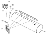
図1は本発明の一実施例を説明するための光走査装置の概略構成図である。図1において、符号101は被走査面である光導電性の感光体ドラム、106は光偏向器である振動ミラー、107は内部に光源とカップリングレンズを有する光源ユニット、113は副走査方向に収束力を有するシリンドリカルレンズ、126は振動ミラー106によって走査された光ビームを感光体ドラム表面へ導光する折り返しミラー、138は有効走査領域外に設けられた同期検知センサ、139は同期検知センサ上にビームを結像させる同期検知用結像レンズ、201は光源ユニット107から出射し振動ミラー106により感光体ドラム101上を走査する光ビームの光路を表している。
[Example 1]
FIG. 1 is a schematic configuration diagram of an optical scanning device for explaining an embodiment of the present invention. In FIG. 1,
光源ユニット107内の光源から射出された光ビームはカップリングレンズにより所定の状態で出射される。本実施例では主走査方向のビームウェスト位置が感光体ドラム101の表面近傍となるような収束状態の光ビームとしている。
The light beam emitted from the light source in the
カップリングレンズ出射後、光ビーム201はシリンドリカルレンズ113にて副走査方向に所定の収束状態とする。カップリングレンズにて主走査方向には所定の収束状態としているが、光源に主に用いられる半導体レーザは、通常主走査方向と副走査方向の発散角が異なり、主走査方向と副走査方向の収束力が略等しいカップリングレンズでは、主走査方向に所定の収束状態としたときに、副走査方向に所望の収束状態とはならない。そこで、副走査方向にのみ収束力を有するシリンドリカルレンズ113にて、副走査方向のビームウェスト位置が感光体表面近傍となるような収束状態としている。
また、副走査方向のビームウェスト位置が感光体表面近傍となるように、シリンドリカルレンズ113が凹のパワー(負の屈折力)を有していても良い。
After exiting the coupling lens, the
Further, the
上述のように整形されたビームは光偏向器としての振動ミラー106に入射する。振動ミラー106の反射面が揺動することにより、被走査面である感光体ドラム101表面を光ビームが走査する。
振動ミラー106により偏向されたビームは折り返しミラー126で感光体ドラム101に導光される。本実施例では折り返しミラーを有する光走査装置の例となっているが、この折り返しミラーを配置せず、直接感光体ドラム101に導光されるように感光体ドラム101を配置しても良い。
The beam shaped as described above is incident on the vibrating
The beam deflected by the vibrating
図2は本実施例における光走査装置に用いる振動ミラーモジュールの分解斜視図を示している。
本実施例では、振動ミラー106の回転トルクの発生方法として電磁駆動方式の例を説明する。
図2に示すように、振動ミラー441は、ねじり梁442で軸支されており、後述するように、単一のSi基板からエッチングにより外形を貫通して作製し、実装基板448に装着され、振動ミラー基板440を構成する。
本実施例では、一対の振動ミラー基板440を背合わせで一体支持したモジュールをなす。
FIG. 2 is an exploded perspective view of the vibrating mirror module used in the optical scanning device according to the present embodiment.
In this embodiment, an example of an electromagnetic drive method will be described as a method for generating the rotational torque of the vibrating
As shown in FIG. 2, the vibrating
In this embodiment, a module in which a pair of vibrating
支持部材447は、樹脂で成形され、回路基板449の所定位置に位置決めされており、振動ミラー基板440を、ねじり梁が主走査平面に直交しミラー面が主走査方向に対し所定の角度、本実施例では22.5°傾くように位置決めする位置決め部451と、振動ミラー基板の実装基板448の一辺に形成されている配線端子455が、装着時に接触するように金属製端子群を配列したエッジコネクタ部452と、を一体で構成している。
The
こうして、振動ミラー基板440は、一辺を上記したエッジコネクタ部452に挿入し、押え爪453の内側に嵌め付け、基板裏側の両側面を位置決め部451に沿わせて支えられるとともに、電気的な配線が同時になされ、各々の振動ミラー基板440が個別に交換できるようにしている。
尚、回路基板449には、後述の振動ミラーの駆動回路を構成する制御ICや水晶発振子などが実装され、コネクタ454を介して電源および制御信号が入出力される。
In this way, the vibrating
The
図3に示すように、振動ミラーモジュール253は、振動ミラーモジュール253を包囲するように立設された側壁257を一体的に形成する光学ハウジング250に装着され、側壁257の上端縁を上カバー258によって封止し、外気から遮断することで、外気の対流による振幅の変化を防止する。また、光ビームを入出射する側壁の開口部には平板状の透過窓259を備えている。
なお、図3において、符号252は光学ハウジング250の別の側壁部に固定される光源ユニットモジュール252(前記の光源ユニット107)、255は光学ハウジング250の光ビームを出射する開口部であり、この開口部255には防塵ガラスを備えている。
As shown in FIG. 3, the
3,
図4は振動ミラー基板440の分解斜視図である。振動ミラー部460は、表面にミラー面を形成し振動子をなす可動部と、それを支え回転軸をなすねじり梁と、支持部をなすフレームとからなり、Si基板をエッチングにより切り抜いて形成する。
本実施例では、SOI基板と呼ばれる60μmと140μmとの2枚の基板が酸化膜を挟んであらかじめ接合されたウエハを用いて作製する。
FIG. 4 is an exploded perspective view of the vibrating
In this embodiment, the wafer is manufactured using a wafer in which two substrates of 60 μm and 140 μm called SOI substrates are bonded in advance with an oxide film interposed therebetween.
まず、140μm基板(第2の基板)461の表面側からプラズマエッチングによるドライプロセスによって、ねじり梁442、平面コイルが形成される振動板443、可動部の骨格をなす補強梁444と、フレーム446とを残したそれ以外の部分を酸化膜まで貫通し、次に、60μm基板(第1の基板)462の表面側からKOHなどの異方性エッチングによって、可動ミラー441と、フレーム447とを残したそれ以外の部分を酸化膜まで貫通し、最後に、可動部周囲の酸化膜を除去して分離し振動ミラーの構造体を形成する。ここで、ねじり梁442、補強梁444の幅は40〜60μmとした。
上記したように振動子の慣性モーメントIは振れ角を大きくとるには小さい方が望ましく、反面、慣性力によってミラー面が変形してしまうため、本実施例では可動部を肉抜きした構造としている。
First, a
As described above, it is desirable that the moment of inertia I of the vibrator is small in order to increase the deflection angle. On the other hand, the mirror surface is deformed by the inertial force. .
さらに、60μm基板462の表面側にアルミニウム薄膜を蒸着して反射面となし、140μm基板461の表面側には銅薄膜でコイルパターン(図示せず)とねじり梁を介して配線された端子(図示せず)、および、トリミング用のパッチ(図示せず)を形成する。当然、振動板443側に薄膜状の永久磁石を備え、フレーム447側に平面コイルを形成する構成とすることもできる。
Further, an aluminum thin film is vapor-deposited on the surface side of the 60
実装基板448上には、振動ミラー部460を装着する枠状の台座466と、振動ミラー部460を囲うように形成されたヨーク449が配備され、上記ヨーク449には可動ミラー端に対向して各々S極とN極とを向かい合わせ、回転軸と直交する方向に磁界を発生する一対の永久磁石450が接合されている。このヨーク449は、実装基板448上に接着剤等によって固定される。
On the mounting
振動ミラー460部は、ミラー面を表に向けて台座466に装着され、図示しない各端子間に電流を流すことによりコイルパターンの回転軸に平行な各辺にローレンツ力が生じ、ねじり梁442をねじって可動ミラー441を回転する回転トルクTを発生し、電流を切るとねじり梁442の戻り力により水平に戻る。
従って、コイルパターンに流れる電流の方向を交互に切り換えることによって、可動ミラー441を往復振動させることができる。
そして、この電流の切り換える周期を、振動ミラーを構成する構造体の、ねじり梁を回転軸とした1次振動モードの固有振動数、いわゆる共振振動数(共振周波数)f0に近づけると振幅が励起され大きな振れ角を得ることができる。
The vibrating
Therefore, the
When the current switching period is made close to the natural frequency of the primary vibration mode with the torsion beam as the rotation axis of the structure constituting the oscillating mirror, the so-called resonance frequency (resonance frequency) f0, the amplitude is excited. A large deflection angle can be obtained.
従って、通常は走査周波数fdをこの共振振動数f0に合わせて設定、あるいは追従するように制御しているが、共振振動数f0は上記したように、振動ミラー460を構成する振動子の慣性モーメントIによって決定されるため、仕上がりの寸法精度にばらつきがあると個体間で差が生じてしまい、複数の振動ミラー部460を用いる場合、各々の走査周波数fdを揃えることが困難となる。
Therefore, the scanning frequency fd is normally set or controlled so as to follow or follow the resonance frequency f0. However, as described above, the resonance frequency f0 is the moment of inertia of the vibrator constituting the
この共振振動数f0のばらつきは、プロセスの能力にもよるが、±200Hz程度あり、例えば、走査周波数fd=2kHzとすると、1/10ラインに相当する走査ラインピッチのずれが生じることになり、A4サイズを出力すると、最終端では数十mmもの倍率ずれになってしまう。
選別によって共振振動数f0の近いものを組み合わせることはできるが、生産効率が悪いうえ、交換を行う際には常に対で扱う必要があるためコストもかかる。
The variation of the resonance frequency f0 is about ± 200 Hz although it depends on the capability of the process. For example, when the scanning frequency fd = 2 kHz, a shift of the scanning line pitch corresponding to 1/10 line occurs. When the A4 size is output, the magnification shift is several tens of mm at the final end.
Those having close resonance frequencies f0 can be combined by sorting, but the production efficiency is poor, and it is necessary to always handle them in pairs when they are exchanged.
そこで、複数の振動ミラーを用いる場合、実装基板に装着する前に、可動部の裏側に形成したパッチ(図示せず)に炭酸ガスレーザなどにより切り込みを入れて可動部の質量を徐々に減らしていくことで慣性モーメントIを調整し、個体間の寸法差があっても共振振動数f0が概略一致するように、本実施例では±50Hzに入るように調整している。
そして、その周波数帯域内で、共振振動数f0によらず、走査周波数fdを設定している。
Therefore, when using a plurality of oscillating mirrors, before mounting on the mounting substrate, a patch (not shown) formed on the back side of the movable part is cut with a carbon dioxide laser or the like to gradually reduce the mass of the movable part. In this embodiment, the inertia moment I is adjusted so as to be within ± 50 Hz so that the resonance frequencies f0 are substantially matched even if there is a dimensional difference between individuals.
The scanning frequency fd is set within the frequency band regardless of the resonance frequency f0.
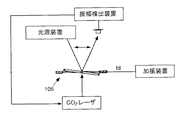
図5は、振動ミラーの質量の可変(トリミング)による共振周波数の調整の様子を示す。振動ミラーには、加振装置により走査周波数に相当する振動が付与され、振動ミラーの裏側よりパッチに炭酸ガス(CO2)レーザが照射され、共振によって急峻に振れ角が増大するまで切込みを入れていく。
共振状態の検出は、振動ミラーの表側から光源装置で光ビームを当て、反射された光ビームの振れを振幅検出装置で検出することにより行うことができる。
尚、このような減量方式のトリミングによらずとも、バランスウエイトを付着していく増量方式の方法によってもよい。
FIG. 5 shows how the resonance frequency is adjusted by changing (trimming) the mass of the vibrating mirror. The vibration mirror is given vibration corresponding to the scanning frequency by the vibration device, and the patch is irradiated with a carbon dioxide (CO 2 ) laser from the back side of the vibration mirror until the deflection angle sharply increases due to resonance. To go.
The resonance state can be detected by applying a light beam with a light source device from the front side of the vibration mirror and detecting a shake of the reflected light beam with an amplitude detection device.
It should be noted that, instead of such a reduction type trimming, an increase type method of attaching a balance weight may be used.
図6は、本実施例の光走査装置における駆動制御系の一例を示すブロック図であり、この駆動制御系は、振動ミラー106の駆動回路601〜603、光源ユニット107内のカップリングレンズ(例えばコリメータレンズ)を駆動させる駆動回路605、光源(LD)の駆動を制御する書込制御系606〜608等を備えている。
上記したように、振動ミラー106の裏側に形成した平面コイルには、交互に電流の流れる方向が切り換わるように、交流電圧、またはパルス波状電圧が印加され、振れ角θが一定となるように平面コイルに流す電流のゲインを調節して往復振動させる。
FIG. 6 is a block diagram illustrating an example of a drive control system in the optical scanning apparatus of the present embodiment. The drive control system includes
As described above, an AC voltage or a pulse wave voltage is applied to the planar coil formed on the back side of the
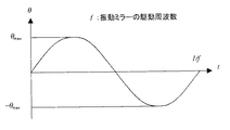
図7は、振動ミラーの平面コイルに流す電流の流れる方向を切り換える周波数fと振れ角θとの関係を示すが、一般に、共振周波数f0をピークとした周波数特性となり、走査周波数fdを共振周波数f0に一致させれば、最も振れ角が大きくとれるが、共振周波数付近においては急峻に振れ角が変化する。
従って、初期的には振動ミラー106の駆動制御部601〜603において固定電極に印加する駆動周波数を共振振動数に合うよう設定することができるが、温度変化に伴うバネ定数の変化などで共振周波数が変動した際には振れ角が激減してしまい、経時的な安定性に乏しいという欠点がある。
FIG. 7 shows the relationship between the frequency f for switching the direction of the current flowing through the planar coil of the oscillating mirror and the deflection angle θ. In general, the frequency characteristic has a resonance frequency f0 as a peak, and the scanning frequency fd is the resonance frequency f0. If they are equal to each other, the deflection angle can be maximized, but the deflection angle changes steeply near the resonance frequency.
Therefore, initially, the
そこで、本実施例では、走査周波数fdを共振周波数f0から外した単一周波数に固定し、ゲイン調整部602のゲイン調整に応じて可動ミラー駆動部603で振れ角θが増減できるようにしている。
具体的には、共振周波数f0=2kHzに対し、走査周波数fdは2.5kHzとし、ゲイン調整により振れ角θが±25°になるように合わせている。
経時的には、振動ミラー106により走査された光ビームを、走査領域の始端に配備した同期検知センサ604において復走査時に検出した検出信号と往走査時に検出した検出信号との時間差により、振幅演算部609で振れ角θを検出し、振れ角θが一定となるようにゲイン調整部602でゲインを調整して可動ミラー駆動部603で振れ角θを制御している。
Therefore, in this embodiment, the scanning frequency fd is fixed to a single frequency that is removed from the resonance frequency f0, and the swing angle θ can be increased or decreased by the movable
Specifically, with respect to the resonance frequency f0 = 2 kHz, the scanning frequency fd is 2.5 kHz, and the deflection angle θ is adjusted to ± 25 ° by gain adjustment.
Over time, the light beam scanned by the
図8に示すように、振動ミラー106は共振振動されるため、時間tとともに正弦波(sin波)状に走査角θが変化する。
従って、振動ミラーの最大振れ角、つまり振幅がθ0とすると、
θ=θ0・sin2πfd・t
となり、同期検知センサ604において走査角を2θsに対応したビームを検出するとすると、検出信号は復走査と往走査とで発生され、その時間差Tを用いると、
θs=θ0・cos2πfd・T/2
で表され、θsは固定であるので、Tを計測すれば最大振れ角θ0が検出できることがわかる。
As shown in FIG. 8, since the
Therefore, if the maximum deflection angle of the vibrating mirror, that is, the amplitude is θ0,
θ = θ0 · sin2πfd · t
When the
θs = θ0 ・ cos2πfd ・ T / 2
Since θs is fixed, it can be seen that the maximum deflection angle θ0 can be detected by measuring T.
尚、復走査でのビーム検出から往走査でのビーム検出に至る期間、振動ミラーの振れ角でいうと、
θ0>θ>θs
なる期間では発光源の発光を禁止するようにしている。
In the period from the beam detection in the backward scan to the beam detection in the forward scan, the deflection angle of the vibrating mirror is
θ0>θ> θs
During a certain period, the light emission of the light source is prohibited.
本実施例の光走査装置では、従来の光走査装置において像面湾曲を補正し、感光体表面上にビームウェスト位置を揃える機能を果たしていた走査レンズを有していない。そのため、本実施例の光走査装置では、図6に示したように、カップリングレンズを振動ミラーと同期させて駆動することにより、像高によってビームウェスト位置を像面上に揃え、像面湾曲を補正している。 The optical scanning device of this embodiment does not have a scanning lens that has the function of correcting the curvature of field and aligning the beam waist position on the surface of the photoreceptor in the conventional optical scanning device. For this reason, in the optical scanning device of this embodiment, as shown in FIG. 6, by driving the coupling lens in synchronism with the vibrating mirror, the beam waist position is aligned on the image plane according to the image height, and the field curvature Is corrected.
ここで、図6を用いて、光源ユニット107内のカップリングレンズの駆動方法について説明する。
上記のように、振動ミラー106の振れ角θが一定となるよう制御するため、同期検知センサ604にて検出している同期信号をモータ駆動部605にも入力し、カップリングレンズを載せたステッピングモータを制御し、カップリングレンズの光軸方向位置を振動ミラー107と同期をとりながら変位させる。
Here, a driving method of the coupling lens in the
As described above, in order to control the swing angle θ of the
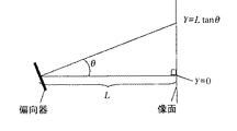
図9に像面湾曲の補正について説明するための光走査装置の概略図を示す。光偏向器である振動ミラーから像面である感光体表面までの距離は、中央像高における光路長より周辺像高における光路長の方が長いので、周辺像高走査時には中央よりもカップリングレンズ通過後のビームが強い収束状態となるようにカップリングレンズの位置を決定する。 FIG. 9 shows a schematic diagram of an optical scanning device for explaining correction of field curvature. Since the optical path length at the peripheral image height is longer than the optical path length at the central image height, the distance from the vibrating mirror as the optical deflector to the photoconductor surface as the image plane is longer than the center during scanning of the peripheral image height. The position of the coupling lens is determined so that the beam after passing is in a strong convergence state.
具体的には、発光点とカップリングレンズ(例えばコリメートレンズ)の位置の違いによる光束の状態には図10のような関係があるので、周辺像高時の発光点からカップリングレンズの前側主点までの距離より長くすれば良い。このような配置にしたときに、像面湾曲が良く補正され、像面である感光体表面上でのビームスポット径を均一化し、画像品質を良好なものにすることができる。
また、本実施例のように、シリンドリカルレンズが副走査方向にのみ収束力を持っている場合に限らず、主走査方向にも収束力を有する形状とし、カップリングレンズの位置をより発光点側に近づける配置にしても良い。これにより光量の確保の観点から有利な配置とすることができる。
Specifically, the state of the light flux depending on the position of the light emitting point and the coupling lens (for example, a collimating lens) has a relationship as shown in FIG. It may be longer than the distance to the point. In such an arrangement, the curvature of field is well corrected, the beam spot diameter on the surface of the photoreceptor, which is the image plane, can be made uniform, and the image quality can be improved.
In addition, as in the present embodiment, the cylindrical lens is not limited to having a convergence power only in the sub-scanning direction, but has a shape having a convergence power in the main scanning direction, and the position of the coupling lens is closer to the light emitting point. It may be arranged close to. Thereby, it can be set as an arrangement | positioning advantageous from a viewpoint of ensuring of light quantity.
カップリングレンズを光軸方向に移動させることに伴い、像高間でのカップリング効率も異なってくる。像高間でカップリング効率が異なるとことにより、光量のムラがあると画像品質の劣化を招く恐れがあるので、本実施例では、図17に示す像高と光量の関係のように、被走査面(像面)上の中央像高走査時のビームの光量が、周辺像高走査時のビームの光量より相対的に大きくなるように、折り返しミラー126にシェーディング効果を有する光学素子を用いている。また、折り返しミラーに限らず、光走査装置を構成する光学素子の少なくともいずれか一つに上述したようなシェーディング効果を有する光学素子を配置しても良い。
As the coupling lens is moved in the optical axis direction, the coupling efficiency between image heights also varies. Since the coupling efficiency varies between image heights, unevenness in the amount of light may lead to degradation of image quality. Therefore, in this embodiment, the relationship between the image height and the amount of light shown in FIG. An optical element having a shading effect is used for the
ところで、図8のように正弦波的に振動する振動ミラーを光走査装置に用いた場合、被走査面が本実施例のように直線状だとすると、その走査の等速性を表すリニアリティVは次の式2で表すことができる。
V=Lω/[cos(θ)]2 ・・・(式2)
L:光偏向器(振動ミラー)から被走査面(像面)までの距離
ω:光偏向器(振動ミラー)の角速度
θ:光偏向器の偏向角(振動ミラーの振れ角)
By the way, when a vibrating mirror that vibrates sinusoidally as shown in FIG. 8 is used in an optical scanning device, if the surface to be scanned is linear as in this embodiment, the linearity V representing the constant velocity of scanning is as follows. This can be expressed by the following
V = Lω / [cos (θ)] 2 (Formula 2)
L: Distance from optical deflector (vibrating mirror) to scanned surface (image plane) ω: Angular velocity of optical deflector (vibrating mirror) θ: Deflection angle of optical deflector (vibration angle of vibrating mirror)
尚、リニアリティVとは、中央像高の走査速度に対する周辺像高の走査速度を指しており、言い換えると、単位偏向角度変化分に対する像高変化分を指している。また、このとき、振動ミラーは正弦波的に振動しているので、その角速度ωは下記の式3となる。
The linearity V indicates the scanning speed of the peripheral image height with respect to the scanning speed of the central image height. In other words, the linearity V indicates the change in image height with respect to the change in unit deflection angle. At this time, since the oscillating mirror vibrates in a sinusoidal manner, the angular velocity ω thereof is expressed by the following
上記の式2、式3について、振動ミラーの最大振幅をパラメータにとり、横軸を画角(本実施例においては光偏向器の偏向角(振動ミラーの振れ角)θの略2倍の値をとる)、縦軸を中央像高を基準とした像面上リニアリティとし、プロットしたグラフを図11に示す。図11においては、縦軸のリニアリティの値が0のときに等速走査されるので、前述したように、このリニアリティが大きいと、被走査面(像面)上での走査速度の等速性が失われていることを示している。走査速度の等速性が失われると、主走査方向周辺で画像の歪等が発生し、画像品質の劣化を引き起こすという問題を発生させるため、リニアリティは可能な限り0%に近づけておく必要がある。
In the
これに対しては、図12に示すように、主走査方向の位置に応じて光源のクロック周波数を相対的に異ならせるか、図13に示すように主走査方向の位置に応じてクロックの位相シフト量を相対的に異ならせることが有効である。
より好ましくは、主走査方向の位置に応じて、光源駆動部606のクロック周波数を相対的に異ならせるとともに、クロック位相シフト量を相対的に異ならせることにより、更に効率良くリニアリティを補正することができる。例えば、正弦波的に振動する振動ミラーを用いた書込光学系において、走査レンズを用いてビームスポット径を感光体表面に均一に揃えた場合、その分、設計値の段階でリニアリティが大きく劣化するような書込光学系の性質となる。このとき、設計値として設定しているリニアリティ変動を、光源駆動部606のクロック周波数を可変とすることにより補正し、加工や組付時に発生する公差によるリニアリティの設計値からのばらつきについては、クロック位相シフト量を制御することにより補正する。このように二つの光源の変調クロック制御手段を二段階に使用することにより、振動ミラーと走査レンズを用いた書込光学系におけるリニアリティを精度良く補正することが可能となる。
In contrast, as shown in FIG. 12, the clock frequency of the light source is made relatively different according to the position in the main scanning direction, or the phase of the clock is changed according to the position in the main scanning direction as shown in FIG. It is effective to make the shift amounts relatively different.
More preferably, the linearity can be corrected more efficiently by making the clock frequency of the light
なお、図12、図13は横軸を時間とし、光源駆動部606で1ドットおきに光源のクロック周波数または位相を変調駆動させたときの注入電流の信号をモデル的に示したものである。
このような電気的な光源駆動制御を行うことにより、走査光学系におけるリニアリティの劣化を補正し、走査速度の等速性を保ち、画像品質の劣化を防ぐことができる。
FIGS. 12 and 13 show modeled signals of injected current when the horizontal axis is time, and the light
By performing such electrical light source drive control, it is possible to correct linearity deterioration in the scanning optical system, maintain constant scanning speed, and prevent image quality deterioration.
本実施例の光走査装置では、より好ましくは、被走査面内の有効走査領域内において、該有効走査領域内の略中央における走査速度に対する各走査位置での走査速度(リニアリティ)が、下記の式1の条件を満足する範囲であることが望ましい。 In the optical scanning device of the present embodiment, more preferably, in the effective scanning area in the surface to be scanned, the scanning speed (linearity) at each scanning position with respect to the scanning speed at the approximate center in the effective scanning area is as follows. A range that satisfies the condition of Equation 1 is desirable.
上記の式1を満足するような条件にて振動ミラーを駆動すると、書込光学系に走査レンズを用いず、かつ効率良くリニアリティを補正し、画像品質を向上することができる。これは、上記の主走査方向の位置に応じて光源駆動部606で光源のクロック周波数を相対的に異ならせてリニアリティを補正する方法と、主走査方向の位置に応じてクロック位相シフト量を相対的に異ならせてリニアリティを補正する方法において、限界補正量が定まっており、その補正量は前述のように段差が目立たないような値に設定している。
When the oscillating mirror is driven under a condition that satisfies the above-described Expression 1, linearity can be corrected efficiently without using a scanning lens in the writing optical system, and image quality can be improved. This is because the light
ここで、上記の式1の条件式中のリニアリティの導出方法ついて述べる。
図26に示すように、光偏向器(振動ミラー)から被走査面(像面)までの距離をL、像高をYとし、振動ミラーが図27に示すように、駆動周波数fで正弦振動しているとする。このとき、像面上の像高Yについて、リニアリティVは、以下の式で表される。
Here, a method for deriving the linearity in the conditional expression of the above Equation 1 will be described.
As shown in FIG. 26, the distance from the optical deflector (vibrating mirror) to the surface to be scanned (image plane) is L, the image height is Y, and the vibrating mirror is sinusoidally oscillated at the drive frequency f as shown in FIG. Suppose you are. At this time, for the image height Y on the image plane, the linearity V is expressed by the following equation.
角速度ωについては、正弦振動ミラーの振れ角特性、
θ=θmaxsin2πft ・・・(a)
より、
ω=dθ/dt=2πθmaxfcos2πft・・・(b)
となる。
ここで、(a)式より、2πftは、
2πft=sin-1(θ/θmax) ・・・(a')
となり、(a')式を(b)に代入すると、下記のように前述の式3となる。
For the angular velocity ω, the deflection angle characteristics of the sine vibrating mirror,
θ = θ max sin2πft (a)
Than,
ω = dθ / dt = 2πθ max fcos 2πft (b)
It becomes.
Here, from equation (a), 2πft is
2πft = sin −1 (θ / θmax) (a ′)
When substituting equation (a ′) into equation (b),
ここで、中央像高でのリニアリティV(0)は、
V(0)=Lω0/cos2(0)
ω0=2πθmaxfcos[sin-1(0)]=2πθmaxf
であるから、
V(0)=L・2πθmaxf
であり、中央像高でのリニアリティV(0)を基準とした正弦振動ミラーの振れ角θのときのリニアリティ(V(θ)−V(0))/V(0)は以下のように導出され、これが式1の条件式中のリニアリティである。
Here, the linearity V (0) at the central image height is
V (0) = Lω 0 / cos 2 (0)
ω 0 = 2πθ max fcos [sin −1 (0)] = 2πθ max f
Because
V (0) = L · 2πθ max f
The linearity (V (θ) −V (0)) / V (0) at the deflection angle θ of the sine vibrating mirror with respect to the linearity V (0) at the center image height is derived as follows. This is the linearity in the conditional expression of Equation 1.
図18に官能評価による段差濃度差の識別度を示す。横軸は各画素での位相シフト量であり、この値は、例えば1/16ドットという値は各画素でのシフト量が画素ピッチの1/16単位であることを示している。縦軸は濃度差を識別できなかった評価者の割合であり、この値が大きければ大きいほど電気的補正を加えたときの画像劣化が抑えられていることを示している。図18によると、各画素のシフト量が画素ピッチの1/16単位以下のときに50%以上の評価者が濃度差を識別できておらず、画像の劣化が抑えられている。このことより、限界補正量を、画素ピッチの1/16単位(±12.5%)と設定している。 FIG. 18 shows the degree of difference in level difference due to sensory evaluation. The horizontal axis represents the phase shift amount in each pixel, and this value, for example, a value of 1/16 dot indicates that the shift amount in each pixel is 1/16 unit of the pixel pitch. The vertical axis represents the percentage of evaluators who could not identify the density difference. The larger this value is, the lower the image deterioration when electrical correction is applied. According to FIG. 18, when the shift amount of each pixel is 1/16 unit or less of the pixel pitch, 50% or more of evaluators have not been able to identify the density difference, and image degradation is suppressed. Therefore, the limit correction amount is set to 1/16 unit (± 12.5%) of the pixel pitch.
この限界補正量を超越して光源クロックの制御を行おうとすると、リニアリティを補正するために、画像品質に濃度差等の別の悪影響が出てしまい画像品質の劣化を招いてしまう。以上の理由により、式1を満足する条件にて振動ミラー106を駆動したときに、より効率良く画像品質を向上できる。
例えばθmax=20degのとき、式1が−12.5%を下回らないθが30.3degとなり、θmax=30degのとき、式1が12.5%を上回らないθが27.0degとなる。この値は、書込光学系の光路長や画角などの条件により最適に設計されるべきである。
If an attempt is made to control the light source clock beyond the limit correction amount, the linearity is corrected, so that another adverse effect such as a density difference occurs on the image quality, leading to a deterioration of the image quality. For the above reasons, the image quality can be improved more efficiently when the
For example, when θ max = 20 deg, θ that does not fall below −12.5% of Equation 1 is 30.3 deg, and when θ max = 30 deg, θ that does not exceed 12.5% of Equation 1 becomes 27.0 deg. . This value should be optimally designed according to conditions such as the optical path length and angle of view of the writing optical system.
本実施例の光走査装置において、更に好ましくは、θmax=22deg近傍という条件にて振動ミラーを駆動した場合である。図11から明らかなように、θmax=22degとした場合、振動ミラーを用いた書込光学系を構成する際に多く用いられる有効画角0deg〜30deg近傍の範囲にわたって、リニアリティが1%未満に抑えられており、より効率良くリニアリティを補正し、画像品質の向上を図ることができる。 In the optical scanning device of the present embodiment, it is more preferable that the vibrating mirror is driven under the condition that θ max = 22 deg. As is apparent from FIG. 11, when θmax = 22 deg, the linearity is suppressed to less than 1% over the range of the effective field angle of about 0 deg to 30 deg, which is often used when configuring a writing optical system using a vibrating mirror. Therefore, the linearity can be corrected more efficiently and the image quality can be improved.
[実施例2]
前述の実施例1では図6におけるステッピングモータをカップリングレンズの光軸方向駆動手段としているが、これに代わり、図16に示す光源ユニット700のように、ボイスコイル等のアクチュエータなどを用いても良い。
図16において、光源である半導体レーザ701は、ホルダ部材702の貫通孔703に、図示しないハウジングへの当接面とは反対側から貫通孔703と同軸に圧入されている。ホルダ部材702の上記ハウジングへの当接面側には貫通孔703と同軸に円筒部709が一体に形成され、その内径に沿って、円筒状に巻かれた電磁コイル704が装着されている。符号706はコリメータレンズ等のカップリングレンズを示している。カップリングレンズ706は、発光源からの光ビームを所定の収束状態または発散状態に変換する第1の結像光学系を構成するもので、中空円筒状のレンズセル707の前端大径部内周側に接着固定されている。レンズセル707は小径の後端部が電磁コイル704の中央部に挿入されている。
[Example 2]
In the first embodiment described above, the stepping motor in FIG. 6 is used as the optical axis direction driving means of the coupling lens. Instead of this, an actuator such as a voice coil may be used as in the
In FIG. 16, a
レンズセル707の外周側にはコイルスプリング705が挿入され、電磁コイル704の前端面とレンズセル707の上記大径部の後端面との間に圧縮されて介在している。レンズセル707は、ホルダ部材702の円筒部709の入口側に挿入されて保持され、ホルダ部材702の前端に形成されている突起に外周部が係合し、上記スプリング705の付勢力によるレンズセル707の移動限界を画するようになっている。上記ホルダ部材702の円筒部709の入口はアパーチャを兼ねたキャップ708で封止され、所定の光束径の光ビームが射出される。
A
レンズセル707は金属で形成され、電磁コイル704に電流を流すとスプリング705の弾力に抗してこれを圧縮しながらレンズセル707が電磁コイル704に吸引され、この電流量を制御することで、発光源からカップリングレンズ706に至る距離を自在に可変することができる。このことからわかるとおり、電磁コイル704は、カップリングレンズ706を光軸方向に往復移動させて、被走査面上における結像位置を移動させる結像位置可変手段を構成している。
The
本実施例では電磁コイル704に所定のバイアス電流をかけることで初期位置をセットし、交流電流を印加することで、レンズセル707が円筒部709の内径に沿って往復移動するようにしている。
さらにこの駆動を、図6と同様の駆動回路を用いて、振動ミラー106の走査状態と同期をとりながら駆動し、安定的に像面湾曲を補正し、感光体表面上でのビームスポット径を均一に揃えている。
In this embodiment, the initial position is set by applying a predetermined bias current to the
Further, this drive is driven using the same drive circuit as in FIG. 6 in synchronization with the scanning state of the
[実施例3]
次に第3の実施例として、感光体表面上でのビームスポット径を均一にするために、図23に示すような可変焦点レンズをカップリングレンズに用いた実施例を説明する。この可変焦点レンズをカップリングレンズに用いた光源ユニットの構成例を図24に示す。
このこの光源ユニットは、光源21と、可変焦点レンズ部13からなり、可変焦点レンズ部13は、可変焦点レンズ14と固定対物レンズ15とから構成されている。
[Example 3]
Next, as a third embodiment, an embodiment in which a variable focus lens as shown in FIG. 23 is used as a coupling lens in order to make the beam spot diameter uniform on the surface of the photoreceptor will be described. FIG. 24 shows an example of the configuration of a light source unit using this variable focus lens as a coupling lens.
The light source unit includes a
図23は可変焦点レンズ部13の詳細図であり、この可変焦点レンズ部13の可変焦点レンズ14は、固定対物レンズ15の焦点距離に対して薄形化するため、以下のように構成されている。
円環状のシリコンスペーサ24に対して透光性弾性膜としての薄膜のガラスダイヤフラム25が陽極接合によって接合されている。ガラスダイヤフラム25上には、PZT等の駆動手段としての圧電素子26がスパッタ等の成膜方法によって円環状に形成されている。また、図示はしていないがガラスダイヤフラム25は、中央部になるほど膜厚が徐々に薄肉となる膜厚分布を有するように形成されており、これにより可変焦点レンズ部13の光学収差を低減するようになっている。
FIG. 23 is a detailed view of the
A
固定対物レンズ15は、レンズホルダ29の内周段部と保持リング30との間に挟持された状態で接着等の手段により固定されている。そして、上述した可変焦点レンズ14と固定対物レンズ15とは接着等の手段により外周部が互いに接合されて一体化されている。
圧電素子26に対する駆動によりガラスダイヤフラム25の曲率が変化して可変焦点レンズ部13の焦点距離が変化する。この駆動を振動ミラー106の駆動と同期させることにより、システムとして安定的に像面湾曲変動の抑制が可能となる。
The fixed
Driving the
[実施例4]
次に、第4の実施例として、感光体表面上でのビームスポット径を均一にするために、カップリングレンズを光軸方向に移動させて像面湾曲補正を行うのではなく、深度拡大手段を用いた実施例を図14を用いて説明する。
図14の光走査装置の基本的な構成は、実施例1で説明した図1の構成と同様であるが、実施例1と異なるのは、深度拡大手段301を光源ユニット107と振動ミラー106との間に配置していることである。また、図6で示したような、実施例1で配置されていたカップリングレンズの光軸方向の移動手段を本実施例では配備していない。
[Example 4]
Next, as a fourth embodiment, in order to make the beam spot diameter uniform on the surface of the photosensitive member, the depth expansion means is not used to correct the field curvature by moving the coupling lens in the optical axis direction. An embodiment using this will be described with reference to FIG.
The basic configuration of the optical scanning device of FIG. 14 is the same as the configuration of FIG. 1 described in the first embodiment, but differs from the first embodiment in that the
深度拡大手段301には、例えばサイドローブピーク強度を増大させるような位相型光学素子を設けることで、深度余裕が拡大し、サイドローブピーク強度が強いものの方が、深度余裕の拡大率が大きい。
具体的には、深度拡大素子301として、光源ユニット107と振動ミラー106の間の光路中に、射出瞳上の強度分布を中央部分よりも周辺の4角が高くなるように変換する強度分布変換素子を付加する、あるいは、深度拡大素子301として、光源ユニット107と振動ミラー106の間の光路中に、射出瞳上の光束の位相分布を任意に変換する位相分布変換素子を付加する、あるいは、深度拡大素子301として、光源ユニット107と振動ミラー106の間の光路中に、射出瞳上の位相分布を変換させる位相分布変換素子と強度分布を変換する強度分布変換素子を付加する、あるいは、深度拡大素子301として、位相分布変換素子と強度分布変換素子とを一体化した光学素子を付加する等の構成としたものが挙げられる。
The
Specifically, as the
強度分布を変換する強度分布変換素子の具体例としては、図19のような階段状でバイナリ型の格子構造を有する回折光学素子301A、または図20のようなリング状の構造の回折パターンを有する回折光学素子301B、図21のような四角錐プリズム301Cを用いて対角方向のみの透過率を上げた濃度フィルター、または、図22のような四角錐プリズム301Cを主・副走査方向に対して約45°傾けて用いる方式でも良い。
As a specific example of the intensity distribution conversion element for converting the intensity distribution, there is a diffractive
上記のような種々の深度拡大素子301を、本発明の光走査装置に用いることにより、ビームウェスト径の深度を拡大することが可能となり、前述した走査結像光学系がない場合の像面湾曲を補い、感光体表面上のビームスポット径を各像高によって均一に保つことができる。ひいては、高画質の画像形成を行うことが可能となる。
By using the various
[実施例5]
次に第5の実施例として、光源駆動部が光量調整手段を備えており、該光量調整手段により、被走査面のそれぞれの走査位置において、単位時間当たりの光ビームのエネルギーを均一にする実施例を説明する。
本実施例では、光量調整手段として、光学素子にシェーディング効果を備えるのではなく、光源駆動部にオートパワーコントロール(以下、APCと言う)を用いている。
APCとは半導体レーザの光出力を受光素子によりモニタし、半導体レーザの光出力に比例する受光電流の検出信号により、半導体レーザの順方向電流を所望の値に制御する方式のことである。
[Example 5]
Next, as a fifth embodiment, the light source driving unit is provided with a light amount adjusting means, and the light amount adjusting means makes the energy of the light beam per unit time uniform at each scanning position of the surface to be scanned. An example will be described.
In this embodiment, as the light amount adjusting means, the optical element is not provided with a shading effect, but an auto power control (hereinafter referred to as APC) is used for the light source driving unit.
APC is a system in which the light output of a semiconductor laser is monitored by a light receiving element, and the forward current of the semiconductor laser is controlled to a desired value by a detection signal of a light receiving current proportional to the light output of the semiconductor laser.
半導体レーザが端面発光型半導体レーザの場合、上記受光素子はカップリングレンズに向かって出射する方向と逆方向に出射した光をモニタするフォトダイオードを用いることが多いが、APCを行なう際に、余計なゴースト光が入射すると、上記受光素子で検出する光量が増加してしまう。
例えば、振動ミラー106へのビームの入射角が0のとき、その振動ミラー106の反射面が光源方向に正対しているので、この位置でAPCを行なうと、反射ビームが光源に戻り、受光素子で検出する光量が増加してしまう。そのため、書込みを実施している振動ミラーからのレーザ出力が狙いより少ない発光出力となってしまい、画像濃度が薄くなってしまったり、濃度むらが発生するという問題を生ずる。
そこで、振動ミラー106の上記入射角が0であるときはAPCを行なわないように設定しておく。この構成をとることにより、適切な濃度で、濃度むらの少ない画像出力が可能となる。
When the semiconductor laser is an edge-emitting type semiconductor laser, the light receiving element often uses a photodiode that monitors light emitted in the direction opposite to the direction emitted toward the coupling lens. When a ghost light is incident, the amount of light detected by the light receiving element increases.
For example, when the incident angle of the beam to the
Therefore, it is set so that APC is not performed when the incident angle of the vibrating
[実施例6]
次に第6の実施例として、本発明の光走査装置を搭載した画像形成装置の一例を図15に示す。
この画像形成装置は、4つの画像形成ステーションを備えた多色対応のタンデム型画像形成装置の例であり、一つの画像形成ステーションについて説明すると、感光体ドラム901の周囲には、該感光体ドラム901を高圧に帯電する帯電チャージャ902、光走査装置900からの光ビームにより記録された静電潜像に帯電したトナーを付着して顕像化する現像ローラ903、現像ローラにトナーを補給するトナーカートリッジ904、感光体ドラム901に残ったトナーを掻き取って備蓄するクリーニングケース905が配置されている。感光体ドラム901へは、光走査装置900の前述した振動ミラーの往復走査により1周期で2ライン毎の画像記録が行われる。
[Example 6]
Next, as a sixth embodiment, an example of an image forming apparatus equipped with the optical scanning device of the present invention is shown in FIG.
This image forming apparatus is an example of a multi-color tandem type image forming apparatus having four image forming stations. When one image forming station is described, the
上記した画像形成ステーションは中間転写ベルト906の移動方向に沿って4つ並列されており、この4つの画像形成ステーションによりイエロー、マゼンタ、シアン、ブラックの各トナー画像が感光体ドラム901上に形成された後、図示しない一次転写手段(各感光体ドラムと対向する位置のベルト裏面側に配設される転写ローラ、転写ブラシ、転写チャージャ等)により中間転写ベルト906上にタイミングを合わせて順次転写され、重ね合わされてカラー画像が形成される。各画像形成ステーションはトナー色が異なるだけで、基本的には同一構成である。
Four image forming stations described above are arranged in parallel along the moving direction of the
一方、記録紙Sは給紙トレイ907から給紙コロ908により供給され、レジストローラ対909により副走査方向の記録開始のタイミングに合わせて送りだされ、図示しない二次転写手段(二次転写ローラ、転写ブラシ、転写チャージャ等)により中間転写ベルト906から記録紙Sにトナー画像が転写される。記録紙Sに転写された未定着トナー画像は、定着装置910のローラ対910で定着され、排紙ローラ912により排紙トレイ911に排出される。
On the other hand, the recording paper S is supplied from the
図25は、上記の図15に示す画像形成装置に用いられる光走査装置900の構成例を示す概略斜視図である。図25において、符号101〜104が、図15に示す画像形成装置の感光体ドラム901に相当し、符号105が中間転写ベルト906に相当する。
図25に示す光走査装置は、光源とカップリングレンズの組を2つづつ有し、2本の光ビームを発する光源ユニットを2つ備えており、それぞれ2本の光ビームを発する光源ユニット107,108から出射された各画像形成ステーション用の光ビーム201〜204は、入射ミラー111とシリンドリカルレンズ113を介して一つの振動ミラー106上に主走査方向に長い線像として照射される。
FIG. 25 is a schematic perspective view showing a configuration example of the
The optical scanning device shown in FIG. 25 includes two sets of light sources and coupling lenses, and includes two light source units that emit two light beams. Each of the
振動ミラー106によって偏向走査されたそれぞれの光ビーム201〜204は、折り返しミラー126〜132を介して、イエロー、マゼンタ、シアン、ブラックのそれぞれの色の画像を形成するための感光体ドラム101〜104に導光され、露光によって各感光体ドラム101〜104に各色に対応した静電潜像が形成される。
各感光体ドラム101〜104上に形成された静電潜像は、各画像形成ステーションの現像手段(現像ローラ等)により各色のトナーで現像され、感光体ドラム101〜104上にイエロー、マゼンタ、シアン、ブラックの各色のトナー画像が形成される。
The respective
The electrostatic latent images formed on the
各感光体ドラム101〜104上に形成されたイエロー、マゼンタ、シアン、ブラックのトナー画像は、中間転写ベルト105上にタイミングを合わせて順次転写され、重ね合わされてカラー画像が形成される。中間転写ベルト105上に転写されたカラー画像は、前述したように記録紙に転写され、定着されてカラー画像が得られる。
The yellow, magenta, cyan, and black toner images formed on the respective
なお、図25において、符号141はトナー画像の転写位置や色ずれを検出するために中間転写ベルト状に定期的に形成されるレジストマークであり、このレジストマークは、LED等の発光素子154と集光レンズ156、受光素子155等からなるレジストマーク検知手段によって検出され、その検知信号が図6の書込制御部607に送られ、各光源ユニット107,108の光源の駆動が制御され、位置ずれや色ずれの補正が行われる。
In FIG. 25,
なお、上記の実施例では、中間転写ベルトを用いた構成で説明したが、中間転写ベルトに代えて記録紙搬送ベルトを用い、各感光体ドラム101〜104から記録紙に直接トナー画像を転写する構成としてもよい。
また、光源ユニット107,108に設けられる光源として、複数の発光部を有する半導体レーザアレイや、あるいは複数の半導体レーザを組合わせた光源等の、マルチビーム光源を用いても良く、この場合には、一度の走査で複数のラインを同時に書き込むことが可能となり、画像形成の更なる高速化が達成できる。
In the above embodiment, the configuration using the intermediate transfer belt has been described. However, instead of the intermediate transfer belt, a recording paper conveyance belt is used, and the toner image is directly transferred from the
Further, as a light source provided in the
以上、本発明に係る光走査装置と、その光走査装置を用いた画像形成装置の実施例を説明したが、本発明は提示した実施例の構成のみに限定されるものではなく、種々の変更が可能である。
例えば、タンデム型の画像形成装置に対応する光走査装置の例として、片側走査方式の例を図25に示したが、振動ミラー106を挟んでその両側の対向位置に2系統づつの光学系を配置して、振動ミラー106の両面を偏向反射面として用いる構成とすれば、対向走査方式の光走査装置を容易に実現することができる。
また、本発明に係る光走査装置は、画像形成装置への適用のみならず、光走査型のバーコード読み取り装置、車載用のレーザレーダ装置などへも応用が可能である。
The embodiments of the optical scanning device according to the present invention and the image forming apparatus using the optical scanning device have been described above, but the present invention is not limited only to the configuration of the presented embodiments, and various modifications can be made. Is possible.
For example, as an example of an optical scanning apparatus corresponding to a tandem type image forming apparatus, an example of a one-side scanning system is shown in FIG. 25, but two systems of optical systems are provided at opposite positions on both sides of the vibrating
The optical scanning device according to the present invention can be applied not only to an image forming apparatus but also to an optical scanning bar code reading device, an in-vehicle laser radar device, and the like.
101、102,103,104,901:感光体ドラム(被走査面)
106:振動ミラー(光偏向器)
107,108:光源ユニット
113:シリンドリカルレンズ
126〜132:折り返しミラー
138:同期検知センサ
139:同期検知用結像レンズ
201〜204:光ビーム
250:光学ハウジング
253:振動ミラーモジュール
301:深度拡大素子(深度拡大手段)
440:振動ミラー基板
441:可動ミラー
442:ねじり梁
447:支持部材(フレーム)
448:実装基板
449:回路基板
601:振動ミラーの駆動制御部
602:ゲイン調整部
603:可動ミラー駆動部
604:同期検知センサ
605:モータ駆動部
606:光源駆動部
607:書込制御部
608:画素クロック生成部
610:光量可変データ
700:光源ユニット
900:光走査装置
902:帯電チャージャ
903:現像ローラ
904:トナーカートリッジ
905:クリーニングケース
906:中間転写ベルト
907:給紙トレイ
910:定着装置
101, 102, 103, 104, 901: Photosensitive drum (scanned surface)
106: Vibration mirror (optical deflector)
107, 108: Light source unit 113: Cylindrical lens 126-132: Folding mirror 138: Synchronization detection sensor 139: Imaging lens for synchronization detection 201-204: Light beam 250: Optical housing 253: Vibration mirror module 301: Depth expansion element ( Depth expansion means)
440: Vibration mirror substrate 441: Movable mirror 442: Torsion beam 447: Support member (frame)
448: Mounting board 449: Circuit board 601: Vibration mirror drive control unit 602: Gain adjustment unit 603: Movable mirror drive unit 604: Synchronization detection sensor 605: Motor drive unit 606: Light source drive unit 607: Write control unit 608: Pixel clock generation unit 610: light quantity variable data 700: light source unit 900: optical scanning device 902: charging charger 903: developing roller 904: toner cartridge 905: cleaning case 906: intermediate transfer belt 907: paper feed tray 910: fixing device
Claims (15)
前記最大偏向角θ max が22deg近傍であることを特徴とする光走査装置。 The optical scanning device according to claim 1,
The optical scanning device, wherein the maximum deflection angle θ max is in the vicinity of 22 deg .
前記光源駆動手段によって前記光源の変調クロックを制御することを特徴とする光走査装置。 In the optical scanning device according to any one of claims 1 to 3,
An optical scanning device characterized in that a modulation clock of the light source is controlled by the light source driving means .
前記光源駆動手段は、前記光偏向器の走査に同期させて、前記変調クロックの周波数を可変することを特徴とする光走査装置。 The optical scanning apparatus according to claim 4 Symbol mounting,
The optical scanning device characterized in that the light source driving means changes the frequency of the modulation clock in synchronization with the scanning of the optical deflector .
前記光源駆動手段は、前記光偏向器の走査に同期させて、前記変調クロックの位相を制御することを特徴とする光走査装置。 The optical scanning device according to claim 4 .
The light source driving means controls the phase of the modulation clock in synchronization with scanning of the optical deflector.
前記光源駆動手段は、前記光偏向器の走査に同期させて、前記変調クロックの位相を制御し、かつ、前記変調クロックの周波数を可変することを特徴とする光走査装置。 The optical scanning apparatus according to claim 4 Symbol mounting,
The optical scanning device characterized in that the light source driving means controls the phase of the modulation clock and changes the frequency of the modulation clock in synchronization with the scanning of the optical deflector.
前記光学素子の結像位置を一走査期間内で変化させる結像位置可変手段を有することを特徴とする光走査装置。 The optical scanning device according to any one of claims 1 to 7 ,
An optical scanning device comprising: an imaging position varying means for changing the imaging position of the optical element within one scanning period .
前記結像位置可変手段は、前記光偏向器の走査に同期させて前記光学素子を光軸方向に移動させることを特徴とする光走査装置。 The optical scanning apparatus according to claim 8 Symbol mounting,
The imaging position varying means moves the optical element in the optical axis direction in synchronization with scanning of the optical deflector .
該光走査装置を構成する少なくともいずれか一つの光学素子は、シェーディング効果を備えており、前記被走査面のそれぞれの走査位置において、単位時間当たりの光ビームのエネルギーを均一にすることを特徴とする光走査装置。 In the optical scanning device according to any one of claims 1 to 9 ,
At least one of the optical elements constituting the optical scanning device has a shading effect, and makes the energy of the light beam per unit time uniform at each scanning position of the surface to be scanned. Optical scanning device.
前記光源駆動手段は、光量調整手段を備えており、該光量調整手段により、前記被走査面のそれぞれの走査位置において、単位時間当たりの光ビームのエネルギーを均一にすることを特徴とする光走査装置。 In the optical scanning device according to any one of claims 1 to 9 ,
The light source driving unit includes a light amount adjusting unit, and the light amount adjusting unit makes the light beam energy per unit time uniform at each scanning position of the surface to be scanned. apparatus.
前記光源を複数備え、該複数の光源からの光ビームを共通の光偏向器で偏向して複数の被走査面を走査することを特徴とする光走査装置。 The optical scanning device according to any one of claims 1 to 11 ,
An optical scanning apparatus comprising a plurality of the light sources, and deflecting light beams from the plurality of light sources with a common optical deflector to scan a plurality of scanned surfaces .
前記被走査面は、光導電性の感光体であることを特徴とする画像形成装置。The image forming apparatus, wherein the scanned surface is a photoconductive photoconductor.
Priority Applications (2)
| Application Number | Priority Date | Filing Date | Title |
|---|---|---|---|
| JP2007031947A JP5228331B2 (en) | 2007-02-13 | 2007-02-13 | Optical scanning apparatus, image forming apparatus, and multicolor image forming apparatus |
| US12/028,446 US8023166B2 (en) | 2007-02-13 | 2008-02-08 | Optical scanning device and image forming apparatus |
Applications Claiming Priority (1)
| Application Number | Priority Date | Filing Date | Title |
|---|---|---|---|
| JP2007031947A JP5228331B2 (en) | 2007-02-13 | 2007-02-13 | Optical scanning apparatus, image forming apparatus, and multicolor image forming apparatus |
Publications (3)
| Publication Number | Publication Date |
|---|---|
| JP2008197336A JP2008197336A (en) | 2008-08-28 |
| JP2008197336A5 JP2008197336A5 (en) | 2010-01-14 |
| JP5228331B2 true JP5228331B2 (en) | 2013-07-03 |
Family
ID=39685562
Family Applications (1)
| Application Number | Title | Priority Date | Filing Date |
|---|---|---|---|
| JP2007031947A Expired - Fee Related JP5228331B2 (en) | 2007-02-13 | 2007-02-13 | Optical scanning apparatus, image forming apparatus, and multicolor image forming apparatus |
Country Status (2)
| Country | Link |
|---|---|
| US (1) | US8023166B2 (en) |
| JP (1) | JP5228331B2 (en) |
Families Citing this family (44)
| Publication number | Priority date | Publication date | Assignee | Title |
|---|---|---|---|---|
| US7468824B2 (en) * | 2004-01-19 | 2008-12-23 | Ricoh Company, Ltd. | Imaging apparatus including optical scanning device with deflecting mirror module, and method of deflecting with the mirror module |
| US20050190420A1 (en) | 2004-02-18 | 2005-09-01 | Shigeaki Imai | Beam-spot position compensation method, optical scanning device, and multi-color image forming device |
| US7800641B2 (en) * | 2007-08-20 | 2010-09-21 | Ricoh Company, Ltd. | Light source unit, optical scan apparatus, and image formation apparatus |
| US7710445B2 (en) * | 2007-08-31 | 2010-05-04 | Ricoh Company, Ltd. | Light source unit, optical scan apparatus, and image formation apparatus |
| JP2009066803A (en) * | 2007-09-11 | 2009-04-02 | Ricoh Co Ltd | Optical scanner, writing method, and image formation device |
| JP4997516B2 (en) * | 2007-09-13 | 2012-08-08 | 株式会社リコー | Optical scanning apparatus and image forming apparatus |
| JP2009069504A (en) * | 2007-09-13 | 2009-04-02 | Ricoh Co Ltd | Optical scanner, and image forming apparatus |
| JP5476659B2 (en) * | 2007-09-14 | 2014-04-23 | 株式会社リコー | Multi-beam optical scanning device and image forming apparatus |
| US8610985B2 (en) * | 2007-12-13 | 2013-12-17 | Ricoh Company, Ltd. | Optical scanning device and image forming apparatus |
| JP2009192563A (en) | 2008-02-12 | 2009-08-27 | Ricoh Co Ltd | Optical scanning device and image forming apparatus |
| JP5343370B2 (en) * | 2008-03-04 | 2013-11-13 | 株式会社リコー | Optical scanning apparatus and image forming apparatus |
| JP5338091B2 (en) * | 2008-03-07 | 2013-11-13 | 株式会社リコー | Optical scanning apparatus and image forming apparatus |
| JP2009214396A (en) * | 2008-03-10 | 2009-09-24 | Ricoh Co Ltd | Optical writing head and image forming apparatus |
| JP5309627B2 (en) * | 2008-03-11 | 2013-10-09 | 株式会社リコー | Optical scanning apparatus and image forming apparatus |
| JP2010055051A (en) | 2008-07-31 | 2010-03-11 | Ricoh Co Ltd | Optical scanning device, control method thereof, and image forming apparatus therewith |
| JP5531458B2 (en) * | 2008-08-01 | 2014-06-25 | 株式会社リコー | Speed detection device and multicolor image forming apparatus |
| JP5078836B2 (en) * | 2008-10-15 | 2012-11-21 | 株式会社リコー | Optical scanning apparatus and image forming apparatus |
| JP5218081B2 (en) * | 2009-01-16 | 2013-06-26 | 株式会社リコー | Light source device, light beam scanning device, and image forming apparatus |
| US8593701B2 (en) * | 2009-09-04 | 2013-11-26 | Ricoh Company, Ltd. | Optical scanning device and image forming apparatus |
| JP4825295B2 (en) * | 2009-10-21 | 2011-11-30 | 日高精機株式会社 | Processing oil application equipment |
| JP5568958B2 (en) | 2009-11-02 | 2014-08-13 | 株式会社リコー | Exposure apparatus and image forming apparatus |
| JP2011100007A (en) * | 2009-11-06 | 2011-05-19 | Ricoh Co Ltd | Optical scanning device and image forming apparatus |
| US8913314B2 (en) | 2009-12-14 | 2014-12-16 | Nec Corporation | Scanning device, image display device, and method for controlling image display device |
| JP2012025130A (en) | 2010-07-27 | 2012-02-09 | Ricoh Co Ltd | Image forming apparatus |
| JP2012058465A (en) | 2010-09-08 | 2012-03-22 | Ricoh Co Ltd | Optical scanning device and picture formation device |
| JP2012078669A (en) * | 2010-10-04 | 2012-04-19 | Mitsumi Electric Co Ltd | Optical scanning device and laser pointer |
| JP5691528B2 (en) | 2011-01-07 | 2015-04-01 | 株式会社リコー | Optical scanning apparatus and image forming apparatus |
| JP2012150161A (en) | 2011-01-17 | 2012-08-09 | Ricoh Co Ltd | Optical scanner and image forming device |
| JP5761655B2 (en) | 2011-03-16 | 2015-08-12 | 株式会社リコー | Optical scanning apparatus, image forming apparatus, scanning lens, and forming method of scanning lens |
| JP5945894B2 (en) | 2011-07-11 | 2016-07-05 | 株式会社リコー | Optical scanning apparatus and image forming apparatus |
| JP5903894B2 (en) | 2012-01-06 | 2016-04-13 | 株式会社リコー | Optical scanning apparatus and image forming apparatus |
| JP2013178496A (en) | 2012-02-06 | 2013-09-09 | Ricoh Co Ltd | Optical scanner and image forming apparatus |
| JP5935404B2 (en) | 2012-03-08 | 2016-06-15 | 株式会社リコー | Optical scanning apparatus and image forming apparatus |
| JP5942493B2 (en) | 2012-03-12 | 2016-06-29 | 株式会社リコー | Optical scanning apparatus and image forming apparatus |
| JP5915898B2 (en) | 2012-03-26 | 2016-05-11 | 株式会社リコー | Exposure apparatus and image forming apparatus |
| JP6024212B2 (en) | 2012-05-31 | 2016-11-09 | 株式会社リコー | Method for manufacturing image forming apparatus, method for adjusting light amount of print head, and method for manufacturing process cartridge |
| JP5962909B2 (en) | 2012-07-20 | 2016-08-03 | 株式会社リコー | Imaging optical system, print head, image forming apparatus, and image reading apparatus |
| JP6108160B2 (en) | 2013-03-13 | 2017-04-05 | 株式会社リコー | Imaging optical system, printer head, and image forming apparatus |
| JP5950884B2 (en) * | 2013-10-18 | 2016-07-13 | 増田 麻言 | Optical scanning method and optical scanning device |
| JP6287246B2 (en) | 2014-01-21 | 2018-03-07 | 株式会社リコー | Printhead manufacturing method, printhead, and image forming apparatus |
| JP6489410B2 (en) | 2014-03-17 | 2019-03-27 | 株式会社リコー | Optical scanning apparatus and image forming apparatus |
| JP6417186B2 (en) * | 2014-10-29 | 2018-10-31 | シャープ株式会社 | Optical scanning device and image forming apparatus provided with optical scanning device |
| JP2017016006A (en) | 2015-07-03 | 2017-01-19 | 株式会社リコー | Optical scanner and image display device |
| JP6657897B2 (en) | 2015-12-10 | 2020-03-04 | 株式会社リコー | Mirror member processing method |
Family Cites Families (50)
| Publication number | Priority date | Publication date | Assignee | Title |
|---|---|---|---|---|
| US4037231A (en) * | 1975-12-15 | 1977-07-19 | The Singer Company | Variable clock rate resonant printer with nonlinear correction |
| JPS63311321A (en) * | 1987-06-15 | 1988-12-20 | Sharp Corp | Scanning type optical printer |
| JP2727572B2 (en) * | 1988-07-26 | 1998-03-11 | キヤノン株式会社 | Optical scanning device |
| JP2924200B2 (en) | 1990-01-18 | 1999-07-26 | 富士電機株式会社 | Torsional vibrator and its application element |
| JPH0675180A (en) * | 1992-06-25 | 1994-03-18 | Sony Corp | Multibeam image-forming device |
| JPH08146328A (en) * | 1994-11-25 | 1996-06-07 | Tec Corp | Laser recorder and image reader |
| JPH08286135A (en) | 1995-04-11 | 1996-11-01 | Fuji Xerox Co Ltd | Optical scanning device |
| JPH10269599A (en) | 1997-03-26 | 1998-10-09 | Denso Corp | Optical pickup device |
| JPH1111144A (en) | 1997-06-20 | 1999-01-19 | Kubota Corp | Air conditioner for working vehicle |
| JP3011144B2 (en) | 1997-07-31 | 2000-02-21 | 日本電気株式会社 | Optical scanner and its driving method |
| JP3920487B2 (en) * | 1999-02-25 | 2007-05-30 | 株式会社リコー | Optical scanning device |
| US6775041B1 (en) * | 1999-04-20 | 2004-08-10 | Ricoh Company, Ltd. | Multibeam scanning apparatus |
| US6932271B2 (en) * | 2000-01-27 | 2005-08-23 | Ricoh Company, Ltd. | Optical scan module, optical scanner, optical scan method, image generator and image reader |
| JP4774157B2 (en) * | 2000-04-13 | 2011-09-14 | 株式会社リコー | Multi-beam light source device and optical scanning device |
| JP4975917B2 (en) * | 2001-03-16 | 2012-07-11 | 株式会社リコー | Optical scanning method, optical scanning module, optical scanning device, and image forming apparatus |
| US7423787B2 (en) * | 2001-03-01 | 2008-09-09 | Ricoh Company, Ltd. | Optical scanning module, device, and method, and imaging apparatus |
| US6657765B2 (en) * | 2001-03-01 | 2003-12-02 | Ricoh Company, Ltd. | Optical deflecting unit, optical scanning unit, image forming apparatus, and method of producing optical unit |
| US7170660B2 (en) * | 2001-04-24 | 2007-01-30 | Ricoh Company, Ltd. | Optical scanner and image forming device |
| US7593029B2 (en) * | 2001-08-20 | 2009-09-22 | Ricoh Company, Ltd. | Optical scanning device and image forming apparatus using the same |
| US7068296B2 (en) * | 2001-09-14 | 2006-06-27 | Ricoh Company, Ltd. | Optical scanning device for reducing a dot position displacement at a joint of scanning lines |
| JP3824528B2 (en) * | 2001-12-14 | 2006-09-20 | 株式会社リコー | Multi-beam scanning optical system and image forming apparatus |
| US6972883B2 (en) * | 2002-02-15 | 2005-12-06 | Ricoh Company, Ltd. | Vibration mirror, optical scanning device, and image forming using the same, method for making the same, and method for scanning image |
| US7333254B2 (en) * | 2002-03-15 | 2008-02-19 | Ricoh Company, Ltd. | Optical scanning apparatus, illuminant apparatus and image forming apparatus |
| US7532227B2 (en) * | 2002-07-02 | 2009-05-12 | Ricoh Company, Ltd. | Optical scanner and image forming apparatus |
| JP4430314B2 (en) * | 2003-02-17 | 2010-03-10 | 株式会社リコー | Optical scanning apparatus and image forming apparatus |
| JP4349825B2 (en) | 2003-03-18 | 2009-10-21 | 株式会社リコー | Optical scanning apparatus and image forming apparatus |
| JP4015065B2 (en) * | 2003-05-29 | 2007-11-28 | 株式会社リコー | Optical scanning apparatus and image forming apparatus |
| JP2005024722A (en) * | 2003-06-30 | 2005-01-27 | Ricoh Co Ltd | Oscillation mirror, optical scanner and image formation device |
| US8824022B2 (en) * | 2003-09-18 | 2014-09-02 | Ricoh Company, Ltd. | Optical scanning apparatus and image forming apparatus |
| US7277212B2 (en) * | 2003-09-19 | 2007-10-02 | Ricoh Company, Limited | Optical scanning unit and image forming apparatus |
| JP4174420B2 (en) * | 2003-12-15 | 2008-10-29 | キヤノン株式会社 | Optical deflector |
| JP2005345866A (en) * | 2004-06-04 | 2005-12-15 | Ricoh Co Ltd | Deflection mirror, optical scanner and image forming apparatus |
| US7468824B2 (en) * | 2004-01-19 | 2008-12-23 | Ricoh Company, Ltd. | Imaging apparatus including optical scanning device with deflecting mirror module, and method of deflecting with the mirror module |
| JP2005215571A (en) | 2004-02-02 | 2005-08-11 | Canon Inc | Optical scanner for deflecting light flux by sinusoidal oscillation, and image forming apparatus using the same |
| US7011367B2 (en) * | 2004-02-11 | 2006-03-14 | Prescient Partners, Lp | Universally adjustable slipcover for dining room chairs |
| US20050190420A1 (en) * | 2004-02-18 | 2005-09-01 | Shigeaki Imai | Beam-spot position compensation method, optical scanning device, and multi-color image forming device |
| US7529011B2 (en) * | 2004-04-12 | 2009-05-05 | Ricoh Company, Ltd. | Deflector mirror with regions of different flexural rigidity |
| JP4653473B2 (en) * | 2004-08-06 | 2011-03-16 | 株式会社リコー | Optical scanning device and image forming device |
| JP4440760B2 (en) * | 2004-12-22 | 2010-03-24 | 株式会社リコー | Image forming apparatus |
| JP4855693B2 (en) * | 2005-02-21 | 2012-01-18 | 株式会社リコー | Optical scanning apparatus and image forming apparatus |
| JP4673115B2 (en) * | 2005-04-07 | 2011-04-20 | 株式会社リコー | Optical scanning device and image forming apparatus using the same |
| JP4768348B2 (en) * | 2005-08-04 | 2011-09-07 | 株式会社リコー | Optical scanning apparatus and image forming apparatus |
| JP2007069572A (en) * | 2005-09-09 | 2007-03-22 | Ricoh Co Ltd | Optical scanning device and image forming device |
| JP4843280B2 (en) * | 2005-09-15 | 2011-12-21 | 株式会社リコー | Multi-beam light source device, optical scanning device, and image forming apparatus |
| JP5493240B2 (en) * | 2005-11-21 | 2014-05-14 | 株式会社リコー | Optical scanning apparatus and image forming apparatus |
| US7643046B2 (en) * | 2005-12-21 | 2010-01-05 | Ricoh Company, Ltd. | Laser beam scanning device, image forming apparatus, and laser beam detecting method by the laser beam scanning device |
| JP4955267B2 (en) * | 2005-12-22 | 2012-06-20 | 株式会社リコー | Multi-beam scanning apparatus and image forming apparatus |
| JP5073945B2 (en) * | 2005-12-26 | 2012-11-14 | 株式会社リコー | Optical scanning device and image forming device |
| JP4986479B2 (en) * | 2006-03-03 | 2012-07-25 | 株式会社リコー | Optical scanning apparatus and image forming apparatus |
| JP4909653B2 (en) * | 2006-06-21 | 2012-04-04 | 株式会社リコー | Optical scanning apparatus and image forming apparatus |
-
2007
- 2007-02-13 JP JP2007031947A patent/JP5228331B2/en not_active Expired - Fee Related
-
2008
- 2008-02-08 US US12/028,446 patent/US8023166B2/en not_active Expired - Fee Related
Also Published As
| Publication number | Publication date |
|---|---|
| US20080192323A1 (en) | 2008-08-14 |
| US8023166B2 (en) | 2011-09-20 |
| JP2008197336A (en) | 2008-08-28 |
Similar Documents
| Publication | Publication Date | Title |
|---|---|---|
| JP5228331B2 (en) | Optical scanning apparatus, image forming apparatus, and multicolor image forming apparatus | |
| JP4986479B2 (en) | Optical scanning apparatus and image forming apparatus | |
| JP5073945B2 (en) | Optical scanning device and image forming device | |
| JP4673115B2 (en) | Optical scanning device and image forming apparatus using the same | |
| US7729031B2 (en) | Light-source device, optical scanning device, and image forming apparatus | |
| US7869110B2 (en) | Optical scan apparatus and image formation apparatus | |
| US7760227B2 (en) | Deflector, optical scanning unit, and image forming apparatus | |
| JP4689462B2 (en) | Optical scanning device and image forming device | |
| JP5041835B2 (en) | Optical scanning apparatus and image forming apparatus | |
| JP2008262186A (en) | Optical scanner and image forming apparatus | |
| JP4970865B2 (en) | Deflection device, optical scanning device, and image forming apparatus | |
| JP2004243721A (en) | Image forming apparatus | |
| JP5169776B2 (en) | Optical scanning apparatus and image forming apparatus | |
| JP2008009073A (en) | Optical scanner and image forming apparatus | |
| JP2007086496A (en) | Optical scanner and image forming apparatus | |
| JP5034094B2 (en) | Optical scanning device and image forming apparatus | |
| JP2008191010A (en) | Beam profile measuring apparatus, optical scanner and image forming device | |
| JP2008065045A (en) | Light source device, optical scanner and image forming apparatus | |
| JP2009031364A (en) | Optical scanner and image formation apparatus incorporating the same | |
| JP2010066598A (en) | Optical scanner and image forming apparatus | |
| JP5418965B2 (en) | Optical scanning apparatus and image forming apparatus | |
| JP2008076449A (en) | Optical scanner and image forming apparatus | |
| US7911669B2 (en) | Optical scanning device and image forming apparatus using the same | |
| JP2008070798A (en) | Optical scanner and image forming apparatus | |
| JP2008020481A (en) | Optical scanner and image forming apparatus |
Legal Events
| Date | Code | Title | Description |
|---|---|---|---|
| A521 | Request for written amendment filed |
Free format text: JAPANESE INTERMEDIATE CODE: A523 Effective date: 20091125 |
|
| A621 | Written request for application examination |
Free format text: JAPANESE INTERMEDIATE CODE: A621 Effective date: 20091125 |
|
| A977 | Report on retrieval |
Free format text: JAPANESE INTERMEDIATE CODE: A971007 Effective date: 20110622 |
|
| A131 | Notification of reasons for refusal |
Free format text: JAPANESE INTERMEDIATE CODE: A131 Effective date: 20110628 |
|
| A521 | Request for written amendment filed |
Free format text: JAPANESE INTERMEDIATE CODE: A523 Effective date: 20110809 |
|
| A131 | Notification of reasons for refusal |
Free format text: JAPANESE INTERMEDIATE CODE: A131 Effective date: 20120327 |
|
| A521 | Request for written amendment filed |
Free format text: JAPANESE INTERMEDIATE CODE: A523 Effective date: 20120524 |
|
| TRDD | Decision of grant or rejection written | ||
| A01 | Written decision to grant a patent or to grant a registration (utility model) |
Free format text: JAPANESE INTERMEDIATE CODE: A01 Effective date: 20130219 |
|
| A61 | First payment of annual fees (during grant procedure) |
Free format text: JAPANESE INTERMEDIATE CODE: A61 Effective date: 20130304 |
|
| FPAY | Renewal fee payment (event date is renewal date of database) |
Free format text: PAYMENT UNTIL: 20160329 Year of fee payment: 3 |
|
| R151 | Written notification of patent or utility model registration |
Ref document number: 5228331 Country of ref document: JP Free format text: JAPANESE INTERMEDIATE CODE: R151 |
|
| LAPS | Cancellation because of no payment of annual fees |