JP5228317B2 - Plasma display apparatus and driving method of plasma display panel - Google Patents
Plasma display apparatus and driving method of plasma display panel Download PDFInfo
- Publication number
- JP5228317B2 JP5228317B2 JP2006330195A JP2006330195A JP5228317B2 JP 5228317 B2 JP5228317 B2 JP 5228317B2 JP 2006330195 A JP2006330195 A JP 2006330195A JP 2006330195 A JP2006330195 A JP 2006330195A JP 5228317 B2 JP5228317 B2 JP 5228317B2
- Authority
- JP
- Japan
- Prior art keywords
- sustain
- discharge
- voltage
- period
- panel
- Prior art date
- Legal status (The legal status is an assumption and is not a legal conclusion. Google has not performed a legal analysis and makes no representation as to the accuracy of the status listed.)
- Expired - Fee Related
Links
Images


Landscapes
- Transforming Electric Information Into Light Information (AREA)
- Control Of Indicators Other Than Cathode Ray Tubes (AREA)
- Control Of Gas Discharge Display Tubes (AREA)
Description
本発明は、壁掛けテレビや大型モニターに用いられるプラズマディスプレイ装置およびプラズマディスプレイパネルの駆動方法に関する。 The present invention relates to a plasma display device and a plasma display panel driving method used for a wall-mounted television or a large monitor.
プラズマディスプレイパネル(以下、「パネル」と略記する)として代表的な交流面放電型パネルは、対向配置された前面板と背面板との間に多数の放電セルが形成されている。前面板は、1対の走査電極と維持電極とからなる表示電極対が前面ガラス基板上に互いに平行に複数対形成され、それら表示電極対を覆うように誘電体層および保護層が形成されている。背面板は、背面ガラス基板上に複数の平行なデータ電極と、それらを覆うように誘電体層と、さらにその上にデータ電極と平行に複数の隔壁とがそれぞれ形成され、誘電体層の表面と隔壁の側面とに蛍光体層が形成されている。そして、表示電極対とデータ電極とが立体交差するように前面板と背面板とが対向配置されて密封され、内部の放電空間には、例えば分圧比で5%のキセノンを含む放電ガスが封入されている。ここで表示電極対とデータ電極とが対向する部分に放電セルが形成される。このような構成のパネルにおいて、各放電セル内でガス放電により紫外線を発生させ、この紫外線で赤色(R)、緑色(G)および青色(B)の各色の蛍光体を励起発光させてカラー表示を行っている。 A typical AC surface discharge type panel as a plasma display panel (hereinafter abbreviated as “panel”) has a large number of discharge cells formed between a front plate and a back plate arranged to face each other. In the front plate, a plurality of display electrode pairs each consisting of a pair of scan electrodes and sustain electrodes are formed in parallel with each other on the front glass substrate, and a dielectric layer and a protective layer are formed so as to cover the display electrode pairs. Yes. The back plate has a plurality of parallel data electrodes on the back glass substrate, a dielectric layer so as to cover them, and a plurality of barrier ribs in parallel with the data electrodes formed on the back glass substrate. A phosphor layer is formed on the side walls of the barrier ribs. Then, the front plate and the back plate are arranged opposite to each other so that the display electrode pair and the data electrode are three-dimensionally crossed and sealed, and a discharge gas containing, for example, 5% xenon is enclosed in the internal discharge space. Has been. Here, a discharge cell is formed at a portion where the display electrode pair and the data electrode face each other. In the panel having such a configuration, ultraviolet rays are generated by gas discharge in each discharge cell, and the phosphors of red (R), green (G) and blue (B) colors are excited and emitted by the ultraviolet rays, thereby performing color display. It is carried out.
パネルを駆動する方法としては、サブフィールド法、すなわち、1フィールド期間を複数のサブフィールドに分割した上で、発光させるサブフィールドの組み合わせによって階調表示を行う方法が一般に用いられている。 As a method of driving the panel, a subfield method, that is, a method of performing gradation display by combining subfields to emit light after dividing one field period into a plurality of subfields is generally used.
各サブフィールドは、初期化期間、書込み期間および維持期間を有する。初期化期間では初期化放電を発生し、続く書込み動作に必要な壁電荷を各電極上に形成するとともに、書込み放電を安定して発生させるためのプライミング粒子(放電のための起爆剤=励起粒子)を発生させる。書込み期間では、表示を行うべき放電セルに選択的に書込みパルス電圧を印加して書込み放電を発生させ壁電荷を形成する(以下、この動作を「書込み」とも記す)。そして維持期間では、走査電極と維持電極とからなる表示電極対に交互に維持パルス電圧を印加し、書込み放電を起こした放電セルで維持放電を発生させ、対応する放電セルの蛍光体層を発光させることにより画像表示を行う。 Each subfield has an initialization period, an address period, and a sustain period. In the initializing period, initializing discharge is generated, wall charges necessary for the subsequent address operation are formed on each electrode, and priming particles for stably generating the address discharge (priming agent for discharge = excited particles) ). In the address period, an address pulse voltage is selectively applied to the discharge cells to be displayed to generate an address discharge to form wall charges (hereinafter, this operation is also referred to as “address”). In the sustain period, a sustain pulse voltage is alternately applied to the display electrode pair composed of the scan electrode and the sustain electrode, and a sustain discharge is generated in the discharge cell that has caused the address discharge, and the phosphor layer of the corresponding discharge cell emits light. To display an image.
また、サブフィールド法の中でも、緩やかに変化する電圧波形を用いて初期化放電を行い、さらに維持放電を行った放電セルに対して選択的に初期化放電を行うことで、階調表示に関係しない発光を極力減らしコントラスト比を向上させた駆動方法が開示されている。 In addition, among the subfield methods, initializing discharge is performed using a slowly changing voltage waveform, and further, initializing discharge is selectively performed on discharge cells that have undergone sustain discharge. A driving method is disclosed in which the light emission that is not generated is reduced as much as possible to improve the contrast ratio.
この駆動方法では、例えば、複数のサブフィールドのうち、1つのサブフィールドの初期化期間においては全ての放電セルで初期化放電を発生させる初期化動作(以下、「全セル初期化動作」と略記する)を行い、他のサブフィールドの初期化期間においては維持放電を行った放電セルだけで初期化放電を発生させる初期化動作(以下、「選択初期化動作」と略記する)を行う。このように駆動することによって、画像の表示に関係のない発光は全セル初期化動作の放電にともなう発光のみとなり、黒表示領域の輝度(以下、「黒輝度」と略記する)は全セル初期化動作における微弱発光だけとなって、コントラストの高い画像表示が可能となる(例えば、特許文献1参照)。 In this driving method, for example, among the plurality of subfields, an initialization operation (hereinafter referred to as “all-cell initialization operation”) in which initialization discharge is generated in all discharge cells in the initialization period of one subfield. In the initializing period of the other subfield, an initializing operation (hereinafter abbreviated as “selective initializing operation”) for generating an initializing discharge only in the discharge cells in which the sustain discharge has been performed is performed. By driving in this way, the light emission not related to the image display is only the light emission due to the discharge of the all-cell initialization operation, and the luminance of the black display area (hereinafter abbreviated as “black luminance”) is the initial value of all cells. Only weak light emission in the digitizing operation is possible, and high-contrast image display is possible (for example, see Patent Document 1).
また、上述の特許文献1には、維持期間における最後の維持パルスのパルス幅を他の維持パルスのパルス幅よりも短くし、表示電極対間の壁電荷による電位差を緩和する、いわゆる細幅消去放電についても記載されている。この細幅消去放電を安定して発生させることによって、続くサブフィールドの書込み期間において確実な書込み動作を行うことができ、コントラスト比の高いプラズマディスプレイ装置を実現することができる。
近年においては、パネルの高精細化、大画面化、高輝度化にともない、プラズマディスプレイ装置におけるさらなる表示品質の向上が望まれている。一方、高精細化、大画面化、高輝度化されたパネルでは、書込み放電が不安定となって、表示を行うべき放電セルで書込み放電が発生せず(以下、このような放電セルを「不灯セル」と表記する)、画像表示品質を劣化させる、あるいは、書込み放電を発生させるために必要な電圧が高くなる等の問題が生じてきた。 In recent years, it has been desired to further improve the display quality of the plasma display device as the panel becomes higher in definition, larger in screen, and higher in brightness. On the other hand, in a panel with high definition, large screen, and high brightness, the address discharge becomes unstable, and no address discharge occurs in the discharge cells to be displayed (hereinafter, such discharge cells are referred to as “ The problem has arisen that the voltage necessary for degrading the image display quality or generating the address discharge has increased.
本発明はこのような課題に鑑みなされたものであり、高精細化、大画面化、高輝度化されたパネルであっても、書込み放電を発生させるために必要な電圧を高くすることなく安定した書込み放電を発生させ、画像表示品質を向上させることができるプラズマディスプレイ装置およびパネルの駆動方法を提供することを目的とする。 The present invention has been made in view of such a problem, and even in a panel with high definition, large screen, and high brightness, it is stable without increasing the voltage necessary for generating address discharge. An object of the present invention is to provide a plasma display device and a panel driving method capable of generating the address discharge and improving the image display quality.
本発明のプラズマディスプレイ装置は、走査電極と維持電極とからなる表示電極対を有する放電セルを複数備えたパネルと、放電させる放電セルを選択する書込み期間と、この書込み期間で選択された放電セルで輝度重みに応じた回数の維持放電を発生させる維持期間とを有するサブフィールドを1フィールド期間内に複数設けてパネルを駆動する駆動回路と、温度センサを有しパネルの温度状態を判定するパネル温度判定回路とを備え、駆動回路は、表示電極対の電極間容量に蓄積された電力を回収しその回収した電力を表示電極対に供給する電力回収部と表示電極対のそれぞれを電源電圧にクランプするスイッチング素子およびベース電位にクランプするスイッチング素子を備えたクランプ部とを有する維持パルス発生回路と、表示電極対の電極間の電位差を緩和するための電圧を表示電極対に印加するスイッチング素子とを有し、維持期間においてベース電位から維持放電を発生させる電位に変位する維持パルスを表示電極対に交互に印加するように構成するとともに、維持期間における最後の維持放電を発生させるための維持パルスとその直前の維持パルスとの間に、表示電極対をともにベース電位とする期間を設けるように構成し、かつその期間の長さをパネル温度判定回路からの信号に応じて変更するように構成したことを特徴とする。 A plasma display device according to the present invention includes a panel including a plurality of discharge cells each having a display electrode pair including a scan electrode and a sustain electrode, an address period for selecting a discharge cell to be discharged, and a discharge cell selected in the address period A driving circuit for driving a panel by providing a plurality of subfields having a sustain period for generating a sustain discharge of the number corresponding to the luminance weight in one field period, and a panel having a temperature sensor for determining the temperature state of the panel A temperature determination circuit, and the drive circuit collects the electric power accumulated in the interelectrode capacitance of the display electrode pair and supplies the collected electric power to the display electrode pair, and each of the display electrode pair is set to the power supply voltage. Sustain pulse generation circuit having a switching element to be clamped and a clamp portion having a switching element to be clamped to a base potential, and a display electrode And a switching element for applying a voltage for relaxing the potential difference between the electrodes to the display electrode pair, and alternately applying a sustain pulse that shifts from the base potential to a potential for generating a sustain discharge during the sustain period. And a period in which the display electrode pair is used as a base potential is provided between the sustain pulse for generating the last sustain discharge in the sustain period and the immediately preceding sustain pulse, and The length of the period is changed according to a signal from the panel temperature determination circuit.
この構成により、書込み放電を発生させるために必要な電圧を高くすることなく安定した書込み放電を発生させ、画像表示品質を向上させることができる。 With this configuration, it is possible to generate a stable address discharge without increasing the voltage necessary for generating the address discharge, and to improve the image display quality.
また、このプラズマディスプレイ装置において、パネル温度判定回路は、温度センサが検出した温度とあらかじめ定めた閾値との比較によりパネルの温度状態を判定するように構成し、駆動回路は、パネル温度判定回路において温度センサが検出した温度があらかじめ定めた閾値よりも低いと判定したときには、そうでないときよりも、表示電極対をともにベース電位とする期間を延長する構成を備える。この構成により、パネルの温度があらかじめ定めた閾値よりも低いかそうでないかを判定し、その判定結果にもとづき上述の表示電極対をともにベース電位とする期間を制御することが可能となる。 Further, in this plasma display device, the panel temperature determination circuit is configured to determine the temperature state of the panel by comparing the temperature detected by the temperature sensor with a predetermined threshold, and the drive circuit is provided in the panel temperature determination circuit. When it is determined that the temperature detected by the temperature sensor is lower than a predetermined threshold value, a configuration is provided in which the period during which the display electrode pair is used as the base potential is extended as compared with the case where it is not. With this configuration, it is possible to determine whether or not the panel temperature is lower than a predetermined threshold value, and to control the period during which both of the display electrode pairs are set to the base potential based on the determination result.
また、このプラズマディスプレイ装置において、上述の駆動回路は、最後の維持放電を発生させるための維持パルスを走査電極に印加する前に、走査電極と維持電極の電位をともにベース電位とする期間を設けるように構成し、その期間の長さをパネル温度判定回路からの信号に応じて変更するように構成してもよい。 Further, in this plasma display device, the drive circuit described above provides a period in which the potentials of the scan electrode and the sustain electrode are both set to the base potential before the sustain pulse for generating the last sustain discharge is applied to the scan electrode. The period of the period may be changed in accordance with a signal from the panel temperature determination circuit.
また、本発明は、走査電極と維持電極とからなる表示電極対を有する放電セルを複数備えたパネルの駆動方法であって、放電させる放電セルを選択する書込み期間と、この書込み期間で選択された放電セルで輝度重みに応じた回数の維持放電を発生させる維持期間とを有するサブフィールドを1フィールド期間内に複数設け、維持期間において、ベース電位から維持放電を発生させる電位に変位する維持パルスを表示電極対に交互に印加するとともに、維持期間における最後の維持放電を発生させるための維持パルスとその直前の維持パルスとの間に、表示電極対をともにベース電位とする期間を設け、パネルの温度が所定の温度よりも低いかそうでないかを判定して、所定の温度よりも低いと判定したときには、表示電極対をともにベース電位とする期間を、そうでないときよりも延長して駆動することを特徴とする。 The present invention also relates to a method for driving a panel having a plurality of discharge cells each having a display electrode pair composed of a scan electrode and a sustain electrode, the address period for selecting a discharge cell to be discharged, and the address period selected in this address period. A plurality of subfields having a sustain period for generating a sustain discharge of the number corresponding to the luminance weight in the discharge cell are provided in one field period, and the sustain pulse is displaced from the base potential to a potential for generating the sustain discharge in the sustain period. Are alternately applied to the display electrode pair, and a period in which the display electrode pair is used as a base potential is provided between the sustain pulse for generating the last sustain discharge in the sustain period and the immediately preceding sustain pulse, If the temperature of the display electrode is lower than the predetermined temperature, and if it is determined that the temperature is lower than the predetermined temperature, the display electrode pair is The period for the position, characterized in that extended to drive than otherwise.
この方法により、書込み放電を発生させるために必要な電圧を高くすることなく安定した書込み放電を発生させ、画像表示品質を向上させることができる。 By this method, it is possible to generate a stable address discharge without increasing the voltage necessary for generating the address discharge, and to improve the image display quality.
本発明によれば、書込み放電を発生させるために必要な電圧を高くすることなく安定した書込み放電を発生させ、画像表示品質を向上させることができるプラズマディスプレイ装置およびパネルの駆動方法を提供することが可能となる。 According to the present invention, it is possible to provide a plasma display device and a panel driving method capable of generating stable address discharge without increasing the voltage necessary for generating address discharge and improving image display quality. Is possible.
以下、本発明の実施の形態におけるプラズマディスプレイ装置について、図面を用いて説明する。 Hereinafter, a plasma display device according to an embodiment of the present invention will be described with reference to the drawings.
(実施の形態)
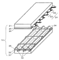
図1は、本発明の一実施の形態におけるパネル10の構造を示す分解斜視図である。ガラス製の前面板21上には、走査電極22と維持電極23とからなる表示電極対24が複数形成されている。そして走査電極22と維持電極23とを覆うように誘電体層25が形成され、その誘電体層25上に保護層26が形成されている。
(Embodiment)
FIG. 1 is an exploded perspective view showing the structure of
また、保護層26は、放電セルにおける放電開始電圧を下げるために、パネルの材料として使用実績があり、ネオン(Ne)およびキセノン(Xe)ガスを封入した場合に2次電子放出係数が大きく耐久性に優れたMgOを主成分とする材料から形成されている。
The
背面板31上にはデータ電極32が複数形成され、データ電極32を覆うように誘電体層33が形成され、さらにその上に井桁状の隔壁34が形成されている。そして、隔壁34の側面および誘電体層33上には赤色(R)、緑色(G)および青色(B)の各色に発光する蛍光体層35が設けられている。
A plurality of
これら前面板21と背面板31とは、微小な放電空間を挟んで表示電極対24とデータ電極32とが交差するように対向配置され、その外周部をガラスフリット等の封着材によって封着されている。そして放電空間には、例えばネオンとキセノンの混合ガスが放電ガスとして封入されている。放電空間は隔壁34によって複数の区画に仕切られており、表示電極対24とデータ電極32とが交差する部分に放電セルが形成されている。そしてこれらの放電セルが放電、発光することにより画像が表示される。
The
なお、パネルの構造は上述したものに限られるわけではなく、例えばストライプ状の隔壁を備えたものであってもよい。 Note that the structure of the panel is not limited to the above-described structure, and for example, a structure having a stripe-shaped partition may be used.
図2は、本発明の一実施の形態におけるパネル10の電極配列図である。パネル10には、行方向に長いn本の走査電極SC1〜SCn(図1の走査電極22)およびn本の維持電極SU1〜SUn(図1の維持電極23)が配列され、列方向に長いm本のデータ電極D1〜Dm(図1のデータ電極32)が配列されている。そして、1対の走査電極SCi(i=1〜n)および維持電極SUiと1つのデータ電極Dj(j=1〜m)とが交差した部分に放電セルが形成され、放電セルは放電空間内にm×n個形成されている。なお、図1、図2に示したように、走査電極SCiと維持電極SUiとは互いに平行に対をなして形成されているために、走査電極SC1〜SCnと維持電極SU1〜SUnとの間に大きな電極間容量Cpが存在する。
FIG. 2 is an electrode array diagram of
次に、パネル10を駆動するための駆動電圧波形とその動作について説明する。本実施の形態におけるプラズマディスプレイ装置は、サブフィールド法、すなわち1フィールド期間を複数のサブフィールドに分割し、サブフィールド毎に各放電セルの発光・非発光を制御することによって階調表示を行う。それぞれのサブフィールドは、初期化期間、書込み期間および維持期間を有する。
Next, a driving voltage waveform for driving
各サブフィールドにおいて、初期化期間では初期化放電を発生し、続く書込み放電に必要な壁電荷を各電極上に形成する。加えて、放電遅れを小さくし書込み放電を安定して発生させるためのプライミング粒子(放電のための起爆剤=励起粒子)を発生させるという働きを持つ。このときの初期化動作には、全ての放電セルで初期化放電を発生させる全セル初期化動作と、1つ前のサブフィールドで維持放電を行った放電セルで初期化放電を発生させる選択初期化動作とがある。 In each subfield, initializing discharge is generated in the initializing period, and wall charges necessary for subsequent address discharge are formed on each electrode. In addition, it has a function of generating priming particles (priming for discharge = excited particles) for reducing discharge delay and generating address discharge stably. The initializing operation at this time includes all-cell initializing operation in which initializing discharge is generated in all discharge cells and selective initializing in which initializing discharge is generated in the discharge cell that has undergone sustain discharge in the previous subfield. There is an operation.
書込み期間では、後に続く維持期間において発光させるべき放電セルで選択的に書込み放電を発生し壁電荷を形成する。そして維持期間では、輝度重みに比例した数の維持パルスを表示電極対24に交互に印加して、書込み放電を発生した放電セルで維持放電を発生させて発光させる。このときの比例定数を「輝度倍率」と呼ぶ。
In the address period, an address discharge is selectively generated in the discharge cells to emit light in the subsequent sustain period to form wall charges. In the sustain period, a number of sustain pulses proportional to the luminance weight are alternately applied to the
なお、本実施の形態では、1フィールドを10のサブフィールド(第1SF、第2SF、・・・、第10SF)で構成し、各サブフィールドはそれぞれ、例えば(1、2、3、6、11、18、30、44、60、80)の輝度重みを持つものとする。そして、第1SFの初期化期間では全セル初期化動作を行い、第2SF〜第10SFの初期化期間では選択初期化動作を行うものとする。そして、各サブフィールドの維持期間においては、それぞれのサブフィールドの輝度重みに所定の輝度倍率を乗じた数の維持パルスを表示電極対のそれぞれに印加する。 In this embodiment, one field is composed of ten subfields (first SF, second SF,..., Tenth SF), and each subfield is, for example, (1, 2, 3, 6, 11). , 18, 30, 44, 60, 80). Then, the all-cell initialization operation is performed in the initialization period of the first SF, and the selective initialization operation is performed in the initialization period of the second SF to the tenth SF. In the sustain period of each subfield, the number of sustain pulses obtained by multiplying the luminance weight of each subfield by a predetermined luminance magnification is applied to each display electrode pair.
しかし、本実施の形態は、サブフィールド数や各サブフィールドの輝度重みが上記の値に限定されるものではなく、また、画像信号等にもとづいてサブフィールド構成を切換える構成であってもよい。 However, in the present embodiment, the number of subfields and the luminance weight of each subfield are not limited to the above values, and the subfield configuration may be switched based on an image signal or the like.
また、本実施の形態では、後述するパネル温度判定回路において判定されるパネル10の温度状態に応じて、維持期間の最後に発生させる消去放電の発生のタイミングを制御している。具体的には、維持期間の最後の維持パルス電圧を印加するタイミングを、パネル10の温度が所定の温度よりも低いときには、そうでないときよりも遅らせている。これにより、書込み放電を発生させるために必要な電圧を高くすることなく安定した書込み放電を発生させることを実現している。以下、駆動電圧波形の概要についてまず説明し、続いて、パネル温度判定回路において、パネル10の温度が所定の温度よりも低いと判定されたときと、所定の温度以上と判定されたときとの駆動電圧波形の違いについて説明する。
In the present embodiment, the timing of occurrence of the erase discharge generated at the end of the sustain period is controlled according to the temperature state of the
図3は、本発明の一実施の形態におけるパネル10の各電極に印加する駆動電圧波形図であり、図4は、図3の部分拡大図である。図3には、2つのサブフィールドの駆動電圧波形、すなわち全セル初期化動作を行うサブフィールド(以下、「全セル初期化サブフィールド」と呼称する)と、選択初期化動作を行うサブフィールド(以下、「選択初期化サブフィールド」と呼称する)とを示しているが、他のサブフィールドにおける駆動電圧波形もほぼ同様である。また、図4は、図3の破線で囲った部分の拡大図であり、維持期間の最後の部分を示す。
FIG. 3 is a waveform diagram of drive voltages applied to each electrode of
まず、全セル初期化サブフィールドである第1SFについて説明する。 First, the first SF, which is an all-cell initialization subfield, will be described.
第1SFの初期化期間前半部では、データ電極D1〜Dm、維持電極SU1〜SUnにそれぞれ0(V)を印加し、走査電極SC1〜SCnには、維持電極SU1〜SUnに対して放電開始電圧以下の電圧Vi1から、放電開始電圧を超える電圧Vi2に向かって緩やかに上昇する傾斜波形電圧(以下、「上りランプ波形電圧」と呼称する)を印加する。 In the first half of the initializing period of the first SF, 0 (V) is applied to the data electrodes D1 to Dm and the sustain electrodes SU1 to SUn, respectively, and the discharge start voltage with respect to the sustain electrodes SU1 to SUn is applied to the scan electrodes SC1 to SCn. A ramp waveform voltage (hereinafter referred to as “up-ramp waveform voltage”) that gradually rises from the voltage Vi1 below toward the voltage Vi2 that exceeds the discharge start voltage is applied.
この上りランプ波形電圧が上昇する間に、走査電極SC1〜SCnと維持電極SU1〜SUn、データ電極D1〜Dmとの間でそれぞれ微弱な初期化放電が持続して起こる。そして、走査電極SC1〜SCn上部に負の壁電圧が蓄積されるとともに、データ電極D1〜Dm上部および維持電極SU1〜SUn上部には正の壁電圧が蓄積される。ここで、電極上部の壁電圧とは電極を覆う誘電体層上、保護層上、蛍光体層上等に蓄積された壁電荷により生じる電圧を表す。 While the rising ramp waveform voltage rises, weak initializing discharges are continuously generated between scan electrodes SC1 to SCn, sustain electrodes SU1 to SUn, and data electrodes D1 to Dm. Negative wall voltage is accumulated on scan electrodes SC1 to SCn, and positive wall voltage is accumulated on data electrodes D1 to Dm and sustain electrodes SU1 to SUn. Here, the wall voltage above the electrode represents a voltage generated by wall charges accumulated on the dielectric layer covering the electrode, the protective layer, the phosphor layer, and the like.
初期化期間後半部では、維持電極SU1〜SUnに正の電圧Ve1を印加し、データ電極D1〜Dmに0(V)を印加し、走査電極SC1〜SCnには、維持電極SU1〜SUnに対して放電開始電圧以下となる電圧Vi3から放電開始電圧を超える電圧Vi4に向かって緩やかに下降する傾斜波形電圧(以下、「下りランプ波形電圧」と呼称する)を印加する。この間に、走査電極SC1〜SCnと維持電極SU1〜SUn、データ電極D1〜Dmとの間でそれぞれ微弱な初期化放電が持続して起こる。そして、走査電極SC1〜SCn上部の負の壁電圧および維持電極SU1〜SUn上部の正の壁電圧が弱められ、データ電極D1〜Dm上部の正の壁電圧は書込み動作に適した値に調整される。以上により、全ての放電セルに対して初期化放電を行う全セル初期化動作が終了する。 In the latter half of the initialization period, positive voltage Ve1 is applied to sustain electrodes SU1 to SUn, 0 (V) is applied to data electrodes D1 to Dm, and scan electrodes SC1 to SCn have sustain electrodes SU1 to SUn. Then, a ramp waveform voltage (hereinafter referred to as “down-ramp waveform voltage”) that gently falls from a voltage Vi3 that is equal to or lower than the discharge start voltage to a voltage Vi4 that exceeds the discharge start voltage is applied. During this time, weak initializing discharges are continuously generated between scan electrodes SC1 to SCn, sustain electrodes SU1 to SUn, and data electrodes D1 to Dm. Then, the negative wall voltage above scan electrodes SC1 to SCn and the positive wall voltage above sustain electrodes SU1 to SUn are weakened, and the positive wall voltage above data electrodes D1 to Dm is adjusted to a value suitable for the write operation. The Thus, the all-cell initializing operation for performing the initializing discharge on all the discharge cells is completed.
続く書込み期間では、維持電極SU1〜SUnに電圧Ve2を、走査電極SC1〜SCnに電圧Vcを印加する。 In the subsequent address period, voltage Ve2 is applied to sustain electrodes SU1 to SUn, and voltage Vc is applied to scan electrodes SC1 to SCn.
まず、1行目の走査電極SC1に負の走査パルス電圧Vaを印加するとともに、データ電極D1〜Dmのうち1行目に発光させるべき放電セルのデータ電極Dk(k=1〜m)に正の書込みパルス電圧Vdを印加する。このときデータ電極Dk上と走査電極SC1上との交差部の電圧差は、外部印加電圧の差(Vd−Va)にデータ電極Dk上の壁電圧と走査電極SC1上の壁電圧との差が加算されたものとなり放電開始電圧を超える。そして、データ電極Dkと走査電極SC1との間および維持電極SU1と走査電極SC1との間に書込み放電が起こり、走査電極SC1上に正の壁電圧が蓄積され、維持電極SU1上に負の壁電圧が蓄積され、データ電極Dk上にも負の壁電圧が蓄積される。 First, the negative scan pulse voltage Va is applied to the scan electrode SC1 in the first row, and the data electrode Dk (k = 1 to m) of the discharge cell to be emitted in the first row among the data electrodes D1 to Dm is positive. The write pulse voltage Vd is applied. At this time, the voltage difference at the intersection between the data electrode Dk and the scan electrode SC1 is the difference between the wall voltage on the data electrode Dk and the wall voltage on the scan electrode SC1 due to the difference in externally applied voltage (Vd−Va). It becomes the sum and exceeds the discharge start voltage. Then, address discharge occurs between data electrode Dk and scan electrode SC1, and between sustain electrode SU1 and scan electrode SC1, positive wall voltage is accumulated on scan electrode SC1, and negative wall is applied on sustain electrode SU1. A voltage is accumulated, and a negative wall voltage is also accumulated on the data electrode Dk.
このようにして、1行目に発光させるべき放電セルで書込み放電を起こして各電極上に壁電圧を蓄積する書込み動作が行われる。一方、書込みパルス電圧Vdを印加しなかったデータ電極D1〜Dmと走査電極SC1との交差部の電圧は放電開始電圧を超えないので、書込み放電は発生しない。以上の書込み動作をn行目の放電セルに至るまで行い、書込み期間が終了する。 In this manner, an address operation is performed in which an address discharge is caused in the discharge cells to be lit in the first row and wall voltage is accumulated on each electrode. On the other hand, the voltage at the intersection of the data electrodes D1 to Dm to which the address pulse voltage Vd is not applied and the scan electrode SC1 does not exceed the discharge start voltage, so that address discharge does not occur. The above address operation is performed until the discharge cell in the nth row, and the address period ends.
続く維持期間では、まず走査電極SC1〜SCnに正の維持パルス電圧Vsを印加するとともに維持電極SU1〜SUnにベース電位となる接地電位、すなわち0(V)を印加する。すると書込み放電を起こした放電セルでは、走査電極SCi上と維持電極SUi上との電圧差が維持パルス電圧Vsに走査電極SCi上の壁電圧と維持電極SUi上の壁電圧との差が加算されたものとなり放電開始電圧を超える。 In the subsequent sustain period, first, positive sustain pulse voltage Vs is applied to scan electrodes SC1 to SCn, and a ground potential that is a base potential, that is, 0 (V) is applied to sustain electrodes SU1 to SUn. Then, in the discharge cell in which the address discharge has occurred, the voltage difference between scan electrode SCi and sustain electrode SUi is the difference between the wall voltage on scan electrode SCi and the wall voltage on sustain electrode SUi. Exceeds the discharge start voltage.
そして、走査電極SCiと維持電極SUiとの間に維持放電が起こり、このとき発生した紫外線により蛍光体層35が発光する。そして走査電極SCi上に負の壁電圧が蓄積され、維持電極SUi上に正の壁電圧が蓄積される。さらにデータ電極Dk上にも正の壁電圧が蓄積される。書込み期間において書込み放電が起きなかった放電セルでは維持放電は発生せず、初期化期間の終了時における壁電圧が保たれる。
Then, a sustain discharge occurs between scan electrode SCi and sustain electrode SUi, and
続いて、走査電極SC1〜SCnにはベース電位となる0(V)を、維持電極SU1〜SUnには維持パルス電圧Vsをそれぞれ印加する。すると、維持放電を起こした放電セルでは、維持電極SUi上と走査電極SCi上との電圧差が放電開始電圧を超えるので再び維持電極SUiと走査電極SCiとの間に維持放電が起こり、維持電極SUi上に負の壁電圧が蓄積され走査電極SCi上に正の壁電圧が蓄積される。以降同様に、走査電極SC1〜SCnと維持電極SU1〜SUnとに交互に輝度重みに輝度倍率を乗じた数の維持パルスを印加し、表示電極対24の電極間に電位差を与えることにより、書込み期間において書込み放電を起こした放電セルで維持放電が継続して行われる。
Subsequently, 0 (V) as a base potential is applied to scan electrodes SC1 to SCn, and sustain pulse voltage Vs is applied to sustain electrodes SU1 to SUn. Then, in the discharge cell in which the sustain discharge has occurred, the voltage difference between the sustain electrode SUi and the scan electrode SCi exceeds the discharge start voltage, so that the sustain discharge occurs again between the sustain electrode SUi and the scan electrode SCi. A negative wall voltage is accumulated on SUi, and a positive wall voltage is accumulated on scan electrode SCi. Thereafter, similarly, the sustain electrodes of the number obtained by multiplying the luminance weight by the luminance magnification are alternately applied to the scan electrodes SC1 to SCn and the sustain electrodes SU1 to SUn, and a potential difference is given between the electrodes of the
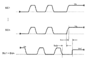
そして、図4にも示すように、維持期間の最後には走査電極SC1〜SCnと維持電極SU1〜SUnとの間にいわゆる細幅パルス状の電圧差を与えて、データ電極Dk上の正の壁電圧を残したまま、走査電極SCiおよび維持電極SUi上の壁電圧を調整している。 As shown in FIG. 4, at the end of the sustain period, a so-called narrow pulse-shaped voltage difference is applied between scan electrodes SC1 to SCn and sustain electrodes SU1 to SUn, and the positive polarity on data electrode Dk is increased. The wall voltage on scan electrode SCi and sustain electrode SUi is adjusted while leaving the wall voltage.
具体的には、維持電極SU1〜SUnを一旦ベース電位となる0(V)に戻した後、維持電極SU1〜SUnと走査電極SC1〜SCnとをともに0(V)に保持する期間(以下、「接地期間ThG」と呼称する)をおき、走査電極SC1〜SCnに維持パルス電圧Vsを印加する。 Specifically, after the sustain electrodes SU1 to SUn are once returned to the base potential of 0 (V), the sustain electrodes SU1 to SUn and the scan electrodes SC1 to SCn are both held at 0 (V) (hereinafter referred to as “V”). (Referred to as “ground period ThG”), and sustain pulse voltage Vs is applied to scan electrodes SC1 to SCn.
すると、維持放電を起こした放電セルの維持電極SUiと走査電極SCiとの間で維持放電が起こる。そしてこの放電が収束する前、すなわち放電で発生した荷電粒子が放電空間内に十分残留している間に、維持電極SU1〜SUnに電圧Ve1を印加する。これにより維持電極SUiと走査電極SCiとの間の電圧差が(Vs−Ve1)の程度まで弱まる。すると、データ電極Dk上の正の壁電荷を残したまま、走査電極SC1〜SCn上と維持電極SU1〜SUn上との間の壁電圧はそれぞれの電極に印加した電圧の差(Vs−Ve1)の程度まで弱められる。以下、この放電を「消去放電」と呼称する。また、消去放電を発生させるために表示電極対24の電極間、すなわち走査電極SC1〜SCnと維持電極SU1〜SUnとの間に与える電位差は、幅の狭い細幅パルス状の電位差である。
Then, a sustain discharge occurs between sustain electrode SUi and scan electrode SCi of the discharge cell in which the sustain discharge has occurred. The voltage Ve1 is applied to the sustain electrodes SU1 to SUn before the discharge converges, that is, while charged particles generated by the discharge remain sufficiently in the discharge space. As a result, the voltage difference between sustain electrode SUi and scan electrode SCi is reduced to the extent of (Vs−Ve1). Then, the wall voltage between the scan electrodes SC1 to SCn and the sustain electrodes SU1 to SUn is the difference between the voltages applied to the respective electrodes (Vs−Ve1) while leaving the positive wall charges on the data electrode Dk. It is weakened to the extent of. Hereinafter, this discharge is referred to as “erase discharge”. Further, the potential difference applied between the electrodes of the
このように、最後の維持放電、すなわち消去放電を発生させるための電圧Vsを走査電極SC1〜SCnに印加した後、所定の時間間隔(以下、「消去位相差Th1」と呼称する)の後、表示電極対24の電極間の電位差を緩和するための電圧Ve1を維持電極SU1〜SUnに印加する。こうして第1SFの維持期間における維持動作が終了する。
Thus, after applying the voltage Vs for generating the last sustain discharge, that is, the erasure discharge, to the scan electrodes SC1 to SCn, after a predetermined time interval (hereinafter referred to as “erasure phase difference Th1”), A voltage Ve1 for reducing the potential difference between the electrodes of the
次に、選択初期化サブフィールドである第2SFの動作について説明する。 Next, the operation of the second SF that is the selective initialization subfield will be described.
第2SFの選択初期化期間では、維持電極SU1〜SUnに電圧Ve1を、データ電極D1〜Dmに0(V)をそれぞれ印加したまま、走査電極SC1〜SCnに電圧Vi3’から電圧Vi4に向かって緩やかに下降する下りランプ波形電圧を印加する。 In the selective initialization period of the second SF, while the voltage Ve1 is applied to the sustain electrodes SU1 to SUn and 0 (V) is applied to the data electrodes D1 to Dm, the voltage Vi3 ′ is applied to the scan electrodes SC1 to SCn from the voltage Vi3 ′ to the voltage Vi4. Apply a ramp-down waveform voltage that gently falls.
すると前のサブフィールドの維持期間で維持放電を起こした放電セルでは微弱な初期化放電が発生し、走査電極SCi上および維持電極SUi上の壁電圧が弱められる。またデータ電極Dkに対しては、直前の維持放電によってデータ電極Dk上に十分な正の壁電圧が蓄積されているので、この壁電圧の過剰な部分が放電され、書込み動作に適した壁電圧に調整される。 Then, a weak initializing discharge is generated in the discharge cell that has caused the sustain discharge in the sustain period of the previous subfield, and the wall voltage on scan electrode SCi and sustain electrode SUi is weakened. For data electrode Dk, a sufficient positive wall voltage is accumulated on data electrode Dk by the last sustain discharge, so that an excessive portion of this wall voltage is discharged, and the wall voltage suitable for the write operation is obtained. Adjusted to
一方、前のサブフィールドで維持放電を起こさなかった放電セルについては放電することはなく、前のサブフィールドの初期化期間終了時における壁電荷がそのまま保たれる。このように選択初期化動作は、直前のサブフィールドの維持期間で維持動作を行った放電セルに対して選択的に初期化放電を行う初期化動作である。 On the other hand, the discharge cells that did not cause the sustain discharge in the previous subfield are not discharged, and the wall charges at the end of the initialization period of the previous subfield are maintained as they are. As described above, the selective initializing operation is an initializing operation in which initializing discharge is selectively performed on the discharge cells that have undergone the sustain operation in the sustain period of the immediately preceding subfield.
続く書込み期間の動作は全セル初期化サブフィールドの書込み期間の動作と同様であるため説明を省略する。続く維持期間の動作も維持パルスの数を除いて同様である。また、第3SF〜第10SFにおいて、初期化期間の動作は第2SFと同様の選択初期化動作であり、書込み期間の書込み動作も第2SFと同様であり、維持期間の動作も維持パルスの数を除いて同様である。 The subsequent operation in the write period is the same as the operation in the write period of the all-cell initialization subfield, and thus the description thereof is omitted. The operation in the subsequent sustain period is the same except for the number of sustain pulses. In the third SF to the tenth SF, the operation in the initialization period is a selective initialization operation similar to that in the second SF, the address operation in the write period is the same as that in the second SF, and the operation in the sustain period also has the number of sustain pulses. It is the same except for this.
ここで、本実施の形態においては、後述するパネル温度判定回路において判定されるパネル10の温度状態に応じて、維持期間の最後に発生させる消去放電の発生のタイミングを制御している。具体的には、消去放電の発生のタイミングを制御するために、維持期間の最後に走査電極SC1〜SCnに維持パルス電圧を印加する直前に表示電極対24をともにベース電位である接地電位に保持する接地期間ThGを設け、その接地期間ThGをパネル温度判定回路において判定されるパネル10の温度状態によって制御している。
Here, in this embodiment, the generation timing of the erasing discharge generated at the end of the sustain period is controlled according to the temperature state of the
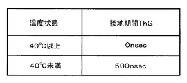
図5は、本発明の一実施の形態におけるパネルの温度状態と接地期間ThGとの関係を示す図である。図5に示すように、本実施の形態では、パネル温度判定回路において判定されるパネル10の温度状態にもとづき接地期間ThGを切換える構成とする。
FIG. 5 is a diagram showing the relationship between the temperature state of the panel and the grounding period ThG in one embodiment of the present invention. As shown in FIG. 5, in the present embodiment, the grounding period ThG is switched based on the temperature state of the
すなわち、パネル温度判定回路においてパネル10の温度が所定の温度以上(本実施の形態では、パネル10の温度が40℃以上)と判定したときは、接地期間ThGを0nsecとし、所定の温度未満(本実施の形態では、パネル10の温度が40℃未満)と判定したときは、接地期間ThGを500nsecとする。
That is, when the panel temperature determination circuit determines that the temperature of the
このように、本実施の形態では、パネル10の温度が所定の温度よりも低いときに、そうでないときよりも、接地期間ThGを延長することで、書込み放電を発生させるために必要な電圧を高くすることなく安定した書込み放電を発生させている。これは、次のような理由による。
As described above, in the present embodiment, when the temperature of the
なお、上述したように、細幅パルスによる消去放電は、放電で発生した荷電粒子が放電空間内に十分残留している間に放電空間内の電界を変化させ、この変化した電界を緩和するように荷電粒子を再配置させて壁電荷を形成することにより所望の壁電荷を形成するものである。そして、この消去放電の放電強度は、接地期間ThGに応じて変化することがわかっている。これは、消去放電の直前の維持放電で形成される壁電荷の状態が接地期間ThGの長さに応じて変化するためと考えられる。そして、接地期間ThGが長くなりすぎると、消去放電が不十分となってしまい、電界を緩和するための荷電粒子が不足して所望の壁電荷が形成できず、本来書込み放電を発生させたいときに壁電圧が不足して書込み放電が発生しないという書込み不良が発生することが確認されている。 As described above, the erasing discharge by the narrow pulse changes the electric field in the discharge space while the charged particles generated in the discharge remain sufficiently in the discharge space, and relaxes the changed electric field. A desired wall charge is formed by rearranging charged particles to form a wall charge. It has been found that the discharge intensity of this erasing discharge changes according to the grounding period ThG. This is presumably because the state of the wall charges formed by the sustain discharge immediately before the erase discharge changes according to the length of the ground period ThG. When the grounding period ThG becomes too long, the erasing discharge becomes insufficient, the charged particles for relaxing the electric field are insufficient, the desired wall charge cannot be formed, and the address discharge is originally generated. It has been confirmed that an address failure occurs such that an address discharge does not occur due to insufficient wall voltage.
そのため、接地期間ThGはそのような書込み不良を発生しないような値に設定することが望ましく、そうすることで、書込みに必要な電圧を高くすることなく、安定した書込み放電を発生させることができる。そして、安定した書込み放電を実現するためには、接地期間ThGを0nsec〜500nsecの範囲で設定することが望ましいという結果が実験により得られた。そこで、本実施の形態においては、この結果にもとづき、接地期間ThGを0nsecと500nsecとで切換えて以下の実験を行った。 Therefore, it is desirable to set the ground period ThG to a value that does not cause such a write failure, and by doing so, it is possible to generate a stable write discharge without increasing the voltage required for the write. . In order to realize a stable address discharge, it has been experimentally obtained that it is desirable to set the ground period ThG in the range of 0 nsec to 500 nsec. Therefore, in the present embodiment, the following experiment was performed by switching the grounding period ThG between 0 nsec and 500 nsec based on this result.
放電特性はパネル10の温度に依存して変化し、放電遅れ(放電を発生させるための電圧を放電セルに印加してから実際に放電が発生するまでの時間遅れのこと)や、暗電流(放電とは無関係に放電セル内に生じる電流のこと)といった放電を不安定にする要素もパネル10の温度に依存して変化する。また、パネル10の温度が低温になると放電セルにおける暗電流が変化して壁電荷の消失(以下、「電荷抜け」と記す)が増加し、不灯セルが発生しやすいことも確認されている。そのため、安定した書込み放電を発生させるために必要な印加電圧はパネル10の温度に依存して変化する。
The discharge characteristics change depending on the temperature of the
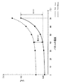
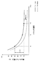
例えば、安定した書込み放電を発生させるために必要な電圧Ve2はパネル10の温度に応じて変化する。図6は、本発明の一実施の形態における安定した書込み放電を発生させるために必要な電圧Ve2とパネルの温度および接地期間ThGとの関係を示す図である。図6において、縦軸は安定した書込み放電を発生させるために必要な電圧Ve2を表し、横軸はパネル10の温度を表す。また、実線は接地期間ThGを0nsecに設定したときを表し、破線は接地期間ThGを500nsecに設定したときを表す。
For example, the voltage Ve <b> 2 necessary for generating a stable address discharge varies depending on the temperature of the
図6に示すように、パネル10の温度が高くなるほど、安定した書込み放電を発生させるために必要な電圧Ve2は高くなる。例えば、接地期間ThGを0nsecに設定した場合では、安定した書込み放電を発生させるために必要な電圧Ve2は、パネル10の温度が約40℃のときには約140(V)であるが、パネル10の温度が約70℃のときには約150(V)となり、約10(V)も高くなる。このように、安定した書込み放電を発生させるために必要な電圧Ve2は、パネル10の温度に応じて変化し、パネル10の温度が高くなるにつれて必要な電圧Ve2は高くなる。
As shown in FIG. 6, the higher the temperature of the
さらに、安定した書込み放電を発生させるために必要な電圧Ve2は、図6に示すように、接地期間ThGによっても変化し、接地期間ThGを500nsecに設定したときには、接地期間ThGを0nsecに設定したときよりも約4(V)高くなることが確認された。 Furthermore, as shown in FIG. 6, the voltage Ve2 required to generate a stable address discharge also changes depending on the ground period ThG. When the ground period ThG is set to 500 nsec, the ground period ThG is set to 0 nsec. It was confirmed that it was about 4 (V) higher than the time.
また、安定した書込み放電を発生させるために必要な書込みパルス電圧Vdもパネル10の温度に応じて変化する。図7は、本発明の一実施の形態における安定した書込み放電を発生させるために必要な書込みパルス電圧Vdとパネルの温度および接地期間ThGとの関係を示す図である。図7において、縦軸は安定した書込み放電を発生させるために必要な書込みパルス電圧Vd(振幅)を表し、横軸はパネル10の温度を表す。また、実線は接地期間ThGを0nsecに設定したときを表し、破線は接地期間ThGを500nsecに設定したときを表す。
Further, the address pulse voltage Vd necessary for generating a stable address discharge also changes according to the temperature of the
図7に示すように、パネル10の温度が低くなるほど、安定した書込み放電を発生させるために必要な書込みパルス電圧Vdは高くなる。例えば、接地期間ThGを0nsecに設定した場合では、安定した書込み放電を発生させるために必要な書込みパルス電圧Vdは、パネル10の温度が約10℃のときには約70(V)であるが、パネル10の温度が約0℃のときには約85(V)となり、約15(V)も高くなる。このように、安定した書込み放電を発生させるために必要な書込みパルス電圧Vdは、パネル10の温度に応じて変化し、パネル10の温度が低くなるにつれて必要な書込みパルス電圧Vdは高くなる。
As shown in FIG. 7, the lower the temperature of
さらに、安定した書込み放電を発生させるために必要な書込みパルス電圧Vdは、図7に示すように、接地期間ThGによっても変化し、接地期間ThGを500nsecに設定したときには、接地期間ThGを0nsecに設定したときよりも、必要な書込みパルス電圧Vdを約5(V)低くできることが確認された。 Further, as shown in FIG. 7, the address pulse voltage Vd necessary for generating a stable address discharge also changes depending on the ground period ThG. When the ground period ThG is set to 500 nsec, the ground period ThG is set to 0 nsec. It was confirmed that the required write pulse voltage Vd can be lowered by about 5 (V) than when it was set.
このように、安定した書込み放電を発生させるために必要な書込みパルス電圧Vdと、安定した書込み放電を発生させるために必要な電圧Ve2とは、パネル10の温度および接地期間ThGに応じて変化することが確認された。さらに、パネル10の温度および接地期間ThGに対して相反する特性を示すことも確認された。
As described above, the address pulse voltage Vd necessary for generating a stable address discharge and the voltage Ve2 required for generating a stable address discharge change according to the temperature of the
ここで、プラズマディスプレイ装置においては、温度に関する動作保証範囲が定められており、その動作保証範囲内において、安定した動作が行われるように、各駆動電圧を設定しなければならない。例えば、電圧Ve2に関しては、上述したようにパネル10の温度が高くなるにつれて安定した書込み放電を発生させるために必要な電圧Ve2は高くなる。したがって、その動作保証範囲内において安定した動作が行われるようにするためには、想定されるパネル10の最高温度において安定した書込み動作がなされるように電圧Ve2を設定しなければならない。また、書込みパルス電圧Vdに関しては、上述したようにパネル10の温度が低くなるにつれて安定した書込み放電を発生させるために必要な書込みパルス電圧Vdは高くなる。したがって、その動作保証範囲内において安定した動作が行われるようにするためには、想定されるパネル10の最低温度において安定した書込み動作がなされるように書込みパルス電圧Vdを設定しなければならない。
Here, in the plasma display device, an operation guarantee range relating to temperature is defined, and each drive voltage must be set so that stable operation is performed within the operation guarantee range. For example, with respect to the voltage Ve2, as described above, the voltage Ve2 required for generating a stable address discharge increases as the temperature of the
一方、上述したように、安定した書込み放電を発生させるために必要な電圧Ve2および書込みパルス電圧Vdは、接地期間ThGによっても変化する。また、放電を安定に発生させるためには、放電を発生させるために必要な駆動電圧と、実際に印加する電圧とのマージンが大きい方がよく、したがってプラズマディスプレイ装置においては、放電に必要な駆動電圧をできるだけ低減することが望ましい。 On the other hand, as described above, the voltage Ve2 and the address pulse voltage Vd necessary for generating a stable address discharge also change depending on the ground period ThG. Also, in order to generate a discharge stably, it is better that the margin between the drive voltage necessary for generating the discharge and the voltage actually applied is large. Therefore, in the plasma display device, the drive necessary for the discharge is required. It is desirable to reduce the voltage as much as possible.
そこで、本実施の形態では、パネル10の温度が40℃以上のときには、接地期間ThGを0nsecに設定するものとする。このような設定とすることで、図6に示すように、接地期間ThGを500nsecに設定するよりも、安定した書込み放電を発生させるために必要な電圧Ve2を低減することができるからである。
Therefore, in the present embodiment, when the temperature of
また、本実施の形態では、パネル10の温度が40℃未満のときには、接地期間ThGを500nsecに設定するものとする。このような設定とすることで、図7に示すように、接地期間ThGを0nsecに設定するよりも、安定した書込み放電を発生させるために必要な書込みパルス電圧Vdを低減することができるからである。特に、安定した書込み放電を発生させるために必要な書込みパルス電圧Vdを低減して、実際に印加する書込みパルス電圧Vdに対するマージンを拡大すると、パネル10の温度が低温のときに発生しやすい不灯セルの発生が低減されることも確認された。
In the present embodiment, when the temperature of
このように、本実施の形態においては、後述するパネル温度判定回路において、パネル10の温度が40℃以上と判定されたときには接地期間ThGを0nsecとし、パネル10の温度が40℃未満と判定されたときには接地期間ThGを500nsecとする構成とする。これにより、書込み放電を発生させるために必要な電圧を高くすることなく安定した書込み放電を発生させ、画像表示品質を向上させることが可能となる。
As described above, in the present embodiment, when the panel temperature determination circuit described later determines that the temperature of the
なお、図6に示すように、接地期間ThGを500nsecに設定すると、安定した書込み放電を発生させるために必要な電圧Ve2は、接地期間ThGを0nsecに設定するよりも高くなる。これはパネル温度が40℃未満のときにおいても同様である。しかし、この電圧Ve2は、接地期間ThGが500nsecでかつパネル温度が40℃のときよりも、接地期間ThGが0nsecでかつパネル温度が70℃のときの方が高い。したがって、例えば、接地期間ThGが0nsecでかつパネル温度が70℃のときに必要な電圧Ve2を基準にして、実際に印加する電圧Ve2を設定すれば、パネル温度が40℃未満のときに接地期間ThGを0nsecから500nsecに切換えても、何ら問題は生じない。そして、これは、書込みパルス電圧Vdについても同様である。 As shown in FIG. 6, when the ground period ThG is set to 500 nsec, the voltage Ve2 required to generate a stable address discharge becomes higher than when the ground period ThG is set to 0 nsec. This is the same when the panel temperature is lower than 40 ° C. However, this voltage Ve2 is higher when the ground period ThG is 0 nsec and the panel temperature is 70 ° C. than when the ground period ThG is 500 nsec and the panel temperature is 40 ° C. Therefore, for example, if the voltage Ve2 actually applied is set on the basis of the voltage Ve2 required when the grounding period ThG is 0 nsec and the panel temperature is 70 ° C., the grounding period is obtained when the panel temperature is lower than 40 ° C. Switching ThG from 0 nsec to 500 nsec does not cause any problem. This also applies to the write pulse voltage Vd.
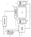
次に、本実施の形態におけるプラズマディスプレイ装置の構成について説明する。図8は、本発明の一実施の形態におけるプラズマディスプレイ装置の回路ブロック図である。プラズマディスプレイ装置1は、パネル10、画像信号処理回路41、データ電極駆動回路42、走査電極駆動回路43、維持電極駆動回路44、タイミング発生回路45、パネル温度判定回路46および各回路ブロックに必要な電源を供給する電源回路(図示せず)を備えている。
Next, the configuration of the plasma display device in the present embodiment will be described. FIG. 8 is a circuit block diagram of the plasma display device according to one embodiment of the present invention. The
画像信号処理回路41は、入力された画像信号sigをサブフィールド毎の発光・非発光を示す画像データに変換する。データ電極駆動回路42はサブフィールド毎の画像データを各データ電極D1〜Dmに対応する信号に変換し各データ電極D1〜Dmを駆動する。
The image
走査電極駆動回路43は、維持パルス発生回路50を備え、タイミング信号にもとづいて走査電極SC1〜SCnに駆動電圧波形を供給する。維持電極駆動回路44は、維持パルス発生回路60および電圧Ve1、Ve2を発生するための回路を備え、タイミング信号にもとづいて維持電極SU1〜SUnに駆動電圧波形を供給する。
Scan
パネル温度判定回路46は、温度を検出するために用いられる熱電対等の一般に知られた素子からなる温度センサ47を有する。そして、温度センサ47で検出されたパネル10周辺の温度からパネル10の温度の推定値を演算により算出し、その算出値とあらかじめ定めた閾値とを比較してパネル10の温度状態を判定して、その結果をタイミング発生回路45に出力する。なお、上述したように、本実施の形態では、この閾値を40℃としているが、これは単なる一例に過ぎず、パネルの特性やプラズマディスプレイ装置の仕様に応じて最適な値に設定すればよい。
The panel
タイミング発生回路45は水平同期信号H、垂直同期信号Vおよびパネル温度判定回路46で判定されたパネル10の温度状態をもとにして各回路ブロックの動作を制御する各種のタイミング信号を発生し、それぞれの回路ブロックへ供給する。そして、上述したように、本実施の形態においては、パネル温度判定回路46においてパネル10の温度が閾値(40℃)よりも低いと判定されたときには、そうでないときよりも接地期間ThGを延長する(0nsecから500nsecに切換える)ように制御しており、それに応じたタイミング信号を走査電極駆動回路43および維持電極駆動回路44に出力する。
The
次に、維持パルス発生回路50、60の詳細とその動作について説明する。図9は、本発明の一実施の形態における維持パルス発生回路50、60の回路図である。なお、図9にはパネル10の電極間容量をCpとして示し、走査パルスおよび初期化電圧波形を発生させる回路は省略している。
Next, the details and operation of sustain
維持パルス発生回路50は、電力回収部51とクランプ部52とを備えている。電力回収部51は、電力回収用のコンデンサC10、スイッチング素子Q11、Q12、逆流防止用のダイオードD11、D12、共振用のインダクタL10を有している。また、クランプ部52は、電圧値がVsである電源VSに走査電極SC1〜SCnをクランプするためのスイッチング素子Q13、および走査電極SC1〜SCnを接地電位にクランプするためのスイッチング素子Q14を有している。そして電力回収部51およびクランプ部52は、走査パルス発生回路(維持期間中は短絡状態となるため図示せず)を介してパネル10の電極間容量Cpの一端である走査電極SC1〜SCnに接続されている。
The sustain
電力回収部51は、電極間容量CpとインダクタL10とをLC共振させて維持パルスの立ち上がりおよび立ち下がりを行う。維持パルスの立ち上がり時には、電力回収用のコンデンサC10に蓄えられている電荷をスイッチング素子Q11、ダイオードD11およびインダクタL10を介して電極間容量Cpに移動する。維持パルスの立ち下がり時には、電極間容量Cpに蓄えられた電荷を、インダクタL10、ダイオードD12およびスイッチング素子Q12を介して電力回収用のコンデンサC10に戻す。こうして走査電極SC1〜SCnへ維持パルスを印加する。このように、電力回収部51は電源から電力を供給されることなくLC共振によって走査電極SC1〜SCnの駆動を行うため、理想的には消費電力が0となる。なお、電力回収用のコンデンサC10は電極間容量Cpに比べて十分に大きい容量を持ち、電力回収部51の電源として働くように構成されており、電源VSの電圧値Vsの半分の約Vs/2に充電されている。
The
電圧クランプ部52は、スイッチング素子Q13を介して走査電極SC1〜SCnを電源VSに接続し、走査電極SC1〜SCnを電圧Vsにクランプする。また、スイッチング素子Q14を介して走査電極SC1〜SCnを接地し、0(V)にクランプする。このようにして電圧クランプ部52は走査電極SC1〜SCnを駆動する。したがって、電圧クランプ部52による電圧印加時のインピーダンスは小さく、強い維持放電による大きな放電電流を安定して流すことができる。
こうして維持パルス発生回路50は、スイッチング素子Q11、Q12、Q13、Q14を制御することによって電力回収部51と電圧クランプ部52とを用いて走査電極SC1〜SCnに維持パルス電圧を印加する。なお、これらのスイッチング素子は、MOSFETやIGBT等の一般に知られた素子を用いて構成することができる。
In this way, sustain
維持パルス発生回路60は、電力回収用のコンデンサC20、スイッチング素子Q21、Q22、逆流防止用のダイオードD21、D22、共振用のインダクタL20を有する電力回収部61と、維持電極SU1〜SUnを電圧Vsにクランプするためのスイッチング素子Q23および維持電極SU1〜SUnを接地電位にクランプするためのスイッチング素子Q24を有するクランプ部62とを備え、パネル10の電極間容量Cpの一端である維持電極SU1〜SUnに接続されている。なお、維持パルス発生回路60の動作は維持パルス発生回路50と同様であるので説明を省略する。
Sustain
また、図9には、表示電極対24の電極間の電位差を緩和するための電圧Ve1を発生する電源VE1、電圧Ve1を維持電極SU1〜SUnに印加するためのスイッチング素子Q26、Q27、電圧ΔVeを発生する電源ΔVE、逆流防止用のダイオードD30、コンデンサC30、電圧Ve1に電圧ΔVeを積み上げて電圧Ve2とするためのスイッチング素子Q28、Q29もあわせて示している。例えば、図3に示した電圧Ve1を印加するタイミングでは、スイッチング素子Q26、Q27を導通させて維持電極SU1〜SUnにダイオードD30、スイッチング素子Q26、Q27を介して正の電圧Ve1を印加する。なお、このときスイッチング素子Q28を導通させ、コンデンサC30の電圧が電圧Ve1になるように充電しておく。また、図3に示した電圧Ve2を印加するタイミングでは、スイッチング素子Q26、Q27は導通させたまま、スイッチング素子Q28を遮断させるとともにスイッチング素子Q29を導通させてコンデンサC30の電圧に電圧ΔVeを重畳し、維持電極SU1〜SUnに電圧Ve1+ΔVe、すなわち電圧Ve2を印加する。このとき、逆流防止用のダイオードD30の働きにより、コンデンサC30から電源VE1への電流は遮断される。
Further, FIG. 9 shows a power source VE1 that generates a voltage Ve1 for relaxing the potential difference between the electrodes of the
なお、電力回収部51のインダクタL10とパネル10の電極間容量CpとのLC共振の周期、および電力回収部61のインダクタL20と同電極間容量CpとのLC共振の周期(以下、「共振周期」と記す)は、インダクタL10、L20のインダクタンスをそれぞれLとすれば、計算式「2π√(LCp)」によって求めることができる。そして、本実施の形態では、電力回収部51、61における共振周期が約1100nsecになるようにインダクタL10、L20を設定しているが、この数値は実施の形態における一例に過ぎず、パネルの特性やプラズマディスプレイ装置の仕様等に合わせて最適な値に設定すればよい。
Note that the period of LC resonance between the inductor L10 of the
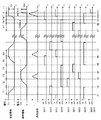
次に、維持期間における駆動電圧波形の詳細について説明する。図10は、本発明の一実施の形態における維持パルス発生回路50、60の動作を説明するためのタイミングチャートであり、図3の破線で囲った部分の詳細なタイミングチャートである。まず維持パルスの1周期をT1〜T6で示した6つの期間に分割し、それぞれの期間について説明する。
Next, details of the drive voltage waveform in the sustain period will be described. FIG. 10 is a timing chart for explaining the operation of sustain
なお、以下の説明においてスイッチング素子を導通させる動作をオン、遮断させる動作をオフと表記し、図面にはスイッチング素子をオンさせる信号を「ON」、オフさせる信号を「OFF」と表記する。 In the following description, the operation for conducting the switching element is expressed as ON and the operation for blocking is expressed as OFF. In the drawing, the signal for turning on the switching element is expressed as “ON”, and the signal for turning off is expressed as “OFF”.
(期間T1)
時刻t1でスイッチング素子Q12をオンにする。すると走査電極SC1〜SCn側の電荷はインダクタL10、ダイオードD12、スイッチング素子Q12を通してコンデンサC10に流れ始め、走査電極SC1〜SCnの電圧が下がり始める。インダクタL10と電極間容量Cpとは共振回路を形成しているので、共振周期の1/2の時間経過後の時刻t2において走査電極SC1〜SCnの電圧は0(V)付近まで低下する。しかし共振回路の抵抗成分等による電力損失のため、走査電極SC1〜SCnの電圧は0(V)までは下がらない。なお、この間、スイッチング素子Q24はオンに保持する。
(Period T1)
At time t1, switching element Q12 is turned on. Then, the charges on the scan electrodes SC1 to SCn side start to flow to the capacitor C10 through the inductor L10, the diode D12, and the switching element Q12, and the voltage on the scan electrodes SC1 to SCn starts to decrease. Since inductor L10 and interelectrode capacitance Cp form a resonance circuit, the voltage of scan electrodes SC1 to SCn drops to near 0 (V) at time t2 after the time ½ of the resonance period has elapsed. However, the voltage of scan electrodes SC1 to SCn does not drop to 0 (V) due to power loss due to the resistance component of the resonance circuit. During this time, the switching element Q24 is kept on.
(期間T2)
そして時刻t2でスイッチング素子Q14をオンにする。すると走査電極SC1〜SCnはスイッチング素子Q14を通して直接に接地されるため、走査電極SC1〜SCnの電圧は強制的に0(V)に低下する。
(Period T2)
At time t2, switching element Q14 is turned on. Then, scan electrodes SC1 to SCn are directly grounded through switching element Q14, so that the voltages of scan electrodes SC1 to SCn are forcibly lowered to 0 (V).
さらに、時刻t2でスイッチング素子Q21をオンにする。すると、電力回収用のコンデンサC20からスイッチング素子Q21、ダイオードD21、インダクタL20を通して電流が流れ始め、維持電極SU1〜SUnの電圧が上がり始める。インダクタL20と電極間容量Cpとは共振回路を形成しているので、共振周期の1/2の時間経過後の時刻t3において維持電極SU1〜SUnの電圧はVs付近まで上昇するが、共振回路の抵抗成分等による電力損失のため、維持電極SU1〜SUnの電圧はVsまでは上がらない。 Further, switching element Q21 is turned on at time t2. Then, a current starts to flow from the power recovery capacitor C20 through the switching element Q21, the diode D21, and the inductor L20, and the voltages of the sustain electrodes SU1 to SUn begin to rise. Since the inductor L20 and the interelectrode capacitance Cp form a resonance circuit, the voltage of the sustain electrodes SU1 to SUn rises to near Vs at time t3 after a time ½ of the resonance period has elapsed. Due to power loss due to the resistance component or the like, the voltage of the sustain electrodes SU1 to SUn does not rise to Vs.
(期間T3)
そして時刻t3でスイッチング素子Q23をオンにする。すると維持電極SU1〜SUnはスイッチング素子Q23を通して直接に電源VSへ接続されるため、維持電極SU1〜SUnの電圧は強制的にVsまで上昇する。すると、書込み放電を起こした放電セルでは走査電極SCi−維持電極SUi間の電圧が放電開始電圧を超え維持放電が発生する。
(Period T3)
At time t3, switching element Q23 is turned on. Then, since sustain electrodes SU1 to SUn are directly connected to power supply VS through switching element Q23, the voltages of sustain electrodes SU1 to SUn are forcibly increased to Vs. Then, in the discharge cell in which the address discharge has occurred, the voltage between scan electrode SCi and sustain electrode SUi exceeds the discharge start voltage, and a sustain discharge occurs.
(期間T4〜T6)
走査電極SC1〜SCnに印加される維持パルスと維持電極SU1〜SUnに印加される維持パルスとは同じ波形であり、期間T4から期間T6までの動作は、期間T1から期間T3までの動作を走査電極SC1〜SCnと維持電極SU1〜SUnとを入れ替えて駆動する動作に等しいので説明を省略する。
(Period T4-T6)
The sustain pulse applied to scan electrodes SC1 to SCn and the sustain pulse applied to sustain electrodes SU1 to SUn have the same waveform, and the operation from period T4 to period T6 scans the operation from period T1 to period T3. Since this is equivalent to the operation of driving the electrodes SC1 to SCn and the sustain electrodes SU1 to SUn, the description thereof will be omitted.
なお、スイッチング素子Q12は時刻t2以降、時刻t5までにオフすればよく、スイッチング素子Q21は時刻t3以降、時刻t4までにオフすればよい。また、スイッチング素子Q22は時刻t5以降、次の時刻t2までにオフすればよく、スイッチング素子Q11は時刻t6以降、次の時刻t1までにオフすればよい。また、維持パルス発生回路50、60の出力インピーダンスを下げるために、スイッチング素子Q24は時刻t2直前に、スイッチング素子Q13は時刻t1直前にオフにすることが望ましく、スイッチング素子Q14は時刻t5直前に、スイッチング素子Q23は時刻t4直前にオフにすることが望ましい。
Switching element Q12 may be turned off after time t2 and before time t5, and switching element Q21 may be turned off after time t3 and before time t4. Further, the switching element Q22 may be turned off after time t5 before the next time t2, and the switching element Q11 may be turned off after time t6 until the next time t1. In order to lower the output impedance of sustain
維持期間においては、以上の期間T1〜T6の動作を、必要なパルス数に応じて繰り返す。このようにして、ベース電位である0(V)から維持放電を発生させる電位である電圧Vsに変位する維持パルス電圧を、表示電極対24のそれぞれに交互に印加して放電セルを維持放電させる。 In the sustain period, the operations in the above periods T1 to T6 are repeated according to the required number of pulses. In this manner, a sustain pulse voltage that shifts from 0 (V), which is the base potential, to a voltage Vs, which is a potential for generating a sustain discharge, is alternately applied to each of the display electrode pairs 24 to sustain discharge the discharge cells. .
次に、維持期間の最後の消去放電について、T7〜T11の5つの期間に分けて詳細に説明する。 Next, the last erasing discharge in the sustain period will be described in detail by dividing it into five periods T7 to T11.
(期間T7)
この期間は、維持電極SU1〜SUnに印加された維持パルスの立ち下がりであり、期間T4と同じである。すなわち、時刻t7直前にスイッチング素子Q23をオフにし時刻t7でスイッチング素子Q22をオンにすることにより、維持電極SU1〜SUn側の電荷はインダクタL20、ダイオードD22、スイッチング素子Q22を通してコンデンサC20に流れ始め、維持電極SU1〜SUnの電圧が下がり始める。
(Period T7)
This period is the fall of the sustain pulse applied to sustain electrodes SU1 to SUn, and is the same as period T4. That is, by turning off the switching element Q23 just before time t7 and turning on the switching element Q22 at time t7, the charges on the sustain electrodes SU1 to SUn side start to flow to the capacitor C20 through the inductor L20, the diode D22, and the switching element Q22. The voltage of sustain electrodes SU1 to SUn begins to drop.
(期間T8)
時刻t8でスイッチング素子Q24をオンにして、維持電極SU1〜SUnの電圧を強制的に0(V)に低下させる。また、スイッチング素子Q14は期間T7からオンに保持され、これにより走査電極SC1〜SCnの電圧も0(V)に保持されたままなので、期間T8では、表示電極対24、すなわち走査電極SC1〜SCn、維持電極SU1〜SUnはともにベース電位である接地電位0(V)に保持されている。
(Period T8)
At time t8, switching element Q24 is turned on to forcibly reduce the voltages of sustain electrodes SU1 to SUn to 0 (V). In addition, since the switching element Q14 is held on from the period T7, and the voltages of the scan electrodes SC1 to SCn are also held at 0 (V), the
このようにして、最後の維持放電を発生させるための維持パルスとその直前の維持パルスとの間に、表示電極対24をともにベース電位である0(V)にクランプして表示電極対24をともにベース電位である0(V)とする期間を設け、接地期間ThGとする。
In this way, the
(期間T9)
時刻t9直前にスイッチング素子Q14をオフにし、時刻t9でスイッチング素子Q11をオンにする。すると、電力回収用のコンデンサC10からスイッチング素子Q11、ダイオードD11、インダクタL10を通して電流が流れ始め、走査電極SC1〜SCnの電圧が上がり始める。
(Period T9)
Switching element Q14 is turned off immediately before time t9, and switching element Q11 is turned on at time t9. Then, current begins to flow from the power recovery capacitor C10 through the switching element Q11, the diode D11, and the inductor L10, and the voltages of the scan electrodes SC1 to SCn begin to rise.
なお、本実施の形態において、接地期間ThGの制御は、維持電極SU1〜SUnを0(V)にクランプするためのスイッチング素子Q24をオンにした後、パネル温度判定回路46におけるパネル10の温度状態の判定結果に応じた時間間隔(本実施の形態では0nsecまたは500nsec)をあけて、走査電極SC1〜SCnに電力回収用のコンデンサC10から電力を供給するためのスイッチング素子Q11をオンにすることで行っている。したがって、スイッチング素子に制御信号を入力してから実際にスイッチング素子がスイッチング動作を開始するまでには、スイッチング素子の遅れ時間等による遅延が発生するが、実用上は、スイッチング素子に入力する制御信号の時間間隔、すなわち時刻t8から時刻t9までを接地期間ThGとみなすことができる。
In this embodiment, the control of the ground period ThG is performed by turning on the switching element Q24 for clamping the sustain electrodes SU1 to SUn to 0 (V), and then the temperature state of the
(期間T10)
インダクタL10と電極間容量Cpとは共振回路を形成しているので、共振周期の1/2の時間経過後には走査電極SC1〜SCnの電圧はVs付近まで上昇するが、ここでは、電力回収部の共振の周期の1/2より短い期間、すなわち走査電極SC1〜SCnの電圧がVs付近まで上昇する以前の時刻t10でスイッチング素子Q13をオンにする。すると走査電極SC1〜SCnはスイッチング素子Q13を通して直接に電源VSへ接続されるため、走査電極SC1〜SCnの電圧は急峻にVsまで上昇し、最後の維持放電が発生する。
(Period T10)
Since the inductor L10 and the interelectrode capacitance Cp form a resonance circuit, the voltage of the scan electrodes SC1 to SCn rises to near Vs after a time ½ of the resonance period has elapsed. Here, the power recovery unit The switching element Q13 is turned on at a time shorter than ½ of the resonance period, that is, at time t10 before the voltage of the scan electrodes SC1 to SCn rises to near Vs. Then, scan electrodes SC1 to SCn are directly connected to power supply VS through switching element Q13, so that the voltage of scan electrodes SC1 to SCn rises sharply to Vs, and the last sustain discharge is generated.
(期間T11)
時刻t11直前にスイッチング素子Q24をオフにし、時刻t11でスイッチング素子Q26、Q27をオンにする。すると維持電極SU1〜SUnはスイッチング素子Q26、Q27を通して直接に消去用の電源VE1へ接続されるため、維持電極SU1〜SUnの電圧は強制的にVe1まで上昇する。この時刻t11は、期間T10で発生した放電が収束する前、すなわち放電で発生した荷電粒子が放電空間内に十分残留している時刻である。そして荷電粒子が放電空間内に十分残留している間に放電空間内の電界が変化するので、この変化した電界を緩和するように荷電粒子が再配置されて壁電荷を形成する。
(Period T11)
Switching element Q24 is turned off immediately before time t11, and switching elements Q26 and Q27 are turned on at time t11. Then, since sustain electrodes SU1 to SUn are directly connected to erasing power supply VE1 through switching elements Q26 and Q27, the voltages of sustain electrodes SU1 to SUn are forcibly increased to Ve1. This time t11 is a time before the discharge generated in the period T10 converges, that is, the charged particles generated by the discharge sufficiently remain in the discharge space. Since the electric field in the discharge space changes while the charged particles remain sufficiently in the discharge space, the charged particles are rearranged to relax the changed electric field to form wall charges.
このとき、維持電極SU1〜SUnに電圧Ve1を印加することで走査電極SC1〜SCnと維持電極SU1〜SUnとの電圧差が小さくなり、走査電極SC1〜SCn上および維持電極SU1〜SUn上の壁電圧は弱められる。このように、最後の維持放電を発生させる電位差は、最後の維持放電が収束する前に表示電極対24の電極間に与える電位差を緩和するように変化させた細幅パルス形状の電位差であり、発生する維持放電は消去放電である。また、図10には示していないが、データ電極D1〜Dmはこのとき0(V)に保持されており、データ電極D1〜Dmに印加されている電圧と走査電極SC1〜SCnに印加されている電圧との電位差を緩和するように放電による荷電粒子が壁電荷を形成するので、データ電極D1〜Dm上には正の壁電圧が形成される。なお、走査電極SC1〜SCnおよび維持電極SU1〜SUn上の壁電荷の極性が変わらないように、電圧Ve1は電圧Vsよりも小さい電圧値としている。
At this time, voltage Ve1 is applied to sustain electrodes SU1 to SUn to reduce the voltage difference between scan electrodes SC1 to SCn and sustain electrodes SU1 to SUn, and walls on scan electrodes SC1 to SCn and sustain electrodes SU1 to SUn. The voltage is weakened. Thus, the potential difference for generating the last sustain discharge is a narrow pulse-shaped potential difference that is changed so as to relax the potential difference applied between the electrodes of the
このようにして、最後の維持放電を発生させるための維持パルスを走査電極SC1〜SCnに印加してから、表示電極対24の電極間の電位差を緩和するための電圧を維持電極SU1〜SUnに印加するまでに所定の時間間隔を設け、その時間間隔を消去位相差Th1とする。
In this way, a sustain pulse for generating the last sustain discharge is applied to scan electrodes SC1 to SCn, and then a voltage for relaxing the potential difference between the electrodes of
以上、説明したように、本実施の形態においては、維持期間における最後の維持放電を発生させるための維持パルスとその直前の維持パルスとの間に、表示電極対24をともにベース電位である接地電位にクランプして表示電極対24をともにベース電位である接地電位とする接地期間ThGを設けるように構成し、かつパネル温度判定回路46からの信号に応じて接地期間ThGを変更するように構成する。すなわち、パネル温度判定回路46において、パネル10の温度が40℃以上と判定されたときには接地期間ThGを0nsecとし、パネル10の温度が40℃未満と判定されたときには接地期間ThGを500nsecとすることで、書込み放電を発生させるために必要な電圧を高くすることなく安定した書込み放電を発生させ、画像表示品質を向上させることが可能となる。
As described above, in the present embodiment, the
なお、電圧Ve1、電圧Ve2を印加する回路については、図9に示した回路に限定されるものではなく、例えば、電圧Ve1を発生させる電源と電圧Ve2を発生させる電源とそれぞれの電圧を維持電極SU1〜SUnに印加するための複数のスイッチング素子とを用いて、それぞれの電圧を必要なタイミングで維持電極SU1〜SUn印加する構成とすることもできる。 Note that the circuit that applies the voltage Ve1 and the voltage Ve2 is not limited to the circuit illustrated in FIG. 9. For example, the power source that generates the voltage Ve1 and the power source that generates the voltage Ve2 and the respective voltages are maintained electrodes. A plurality of switching elements for applying to SU1 to SUn can be used to apply the sustain electrodes SU1 to SUn at necessary timings.
なお、本実施の形態において示した各数値、例えば、パネル温度判定回路46においてパネル10の温度との比較に用いる閾値や接地期間ThG等の数値は、実験に用いた表示電極対数1080の50インチのパネルの特性にもとづくものであって、単に実施の形態の一例を示したに過ぎない。本実施の形態はこれらの数値に何ら限定されるものではなく、パネルの特性やプラズマディスプレイ装置の仕様等に応じて最適な値に設定することが望ましい。また、これらの各数値は、上述した効果を得られる範囲でのばらつきを許容するものである。
Each numerical value shown in the present embodiment, for example, a threshold value used for comparison with the temperature of the
なお、パネル温度判定回路46においてパネル10の温度を判定する際にヒステリシス特性を持たせると、パネル10の温度が閾値付近にある場合に、消去位相差Th1の頻繁な変動を抑制できるのでさらに画像表示品質を向上させることができる。具体的には、パネル10の温度状態定別用に2つの閾値を設け、パネル10の温度が上昇しているときに用いる閾値(例えば、42℃)を、パネル10の温度が低下しているときに用いる閾値(例えば、38℃)よりも高く設定することで、ヒステリシス特性を持たせることが可能である。
If the panel
また、本実施の形態ではパネル10の温度状態を2つに分けて接地期間ThGを切換える構成を説明したが、何らこの構成に限定されるものではなく、例えば、パネル10の温度状態を3つ、あるいはそれ以上に分け、温度が低くなるほど接地期間ThGを延長させるようにしてもよい。
Further, in the present embodiment, the configuration in which the temperature state of the
なお、本発明の実施の形態では、第1SFを全セル初期化サブフィールドとし第2SF〜第10SFを選択初期化サブフィールドとするサブフィールド構成を例に挙げて説明を行ったが、必ずしもこのサブフィールド構成に限定されるものではなく、これ以外のサブフィールド構成であってもかまわない。 In the embodiment of the present invention, the subfield configuration in which the first SF is the all-cell initializing subfield and the second SF to the tenth SF are the selective initializing subfield has been described as an example. It is not limited to the field configuration, and other subfield configurations may be used.
また、本実施の形態では、電力供給用と電力回収用とで同一のインダクタを用いる構成を説明したが、何らこの構成に限定されるものではなく、インダクタンスの異なる複数のインダクタを切換えて用いる構成としてもよい。この構成では、例えば、維持パルスの立ち上がりと立ち下がりとで共振周波数を切換えて駆動する、といったことが可能となる。 Further, in the present embodiment, the configuration in which the same inductor is used for power supply and for power recovery has been described. However, the configuration is not limited to this configuration, and a configuration in which a plurality of inductors having different inductances are switched and used. It is good. In this configuration, for example, it is possible to drive by switching the resonance frequency between the rising edge and the falling edge of the sustain pulse.
また、本実施の形態ではベース電位を接地電位とする構成を説明したが、AC型パネルは放電セルの周囲が誘電体に囲まれており各電極の駆動電圧波形は容量結合的に放電セルに印加されるため、ベース電位を含む各駆動電圧波形はDC的にレベルシフトされていてもよい。 In this embodiment, the base potential is set to the ground potential. However, in the AC panel, the discharge cell is surrounded by a dielectric, and the drive voltage waveform of each electrode is capacitively coupled to the discharge cell. Since the voltage is applied, each drive voltage waveform including the base potential may be level-shifted in a DC manner.
本発明は、書込み放電を発生させるために必要な電圧を高くすることなく安定した書込み放電を発生させ、画像表示品質を向上させることが可能であり、プラズマディスプレイ装置およびパネルの駆動方法として有用である。 INDUSTRIAL APPLICABILITY The present invention can generate stable address discharge without increasing the voltage necessary for generating address discharge and improve image display quality, and is useful as a method for driving a plasma display device and a panel. is there.
1 プラズマディスプレイ装置
10 パネル
21 (ガラス製の)前面板
22 走査電極
23 維持電極
24 表示電極対
25,33 誘電体層
26 保護層
31 背面板
32 データ電極
34 隔壁
35 蛍光体層
41 画像信号処理回路
42 データ電極駆動回路
43 走査電極駆動回路
44 維持電極駆動回路
45 タイミング発生回路
46 パネル温度判定回路
47 温度センサ
50,60 維持パルス発生回路
51,61 電力回収部
52,62 (電圧)クランプ部
Q11,Q12,Q13,Q14,Q21,Q22,Q23,Q24,Q26,Q27,Q28,Q29 スイッチング素子
D11,D12,D21,D22,D30 (逆流防止用の)ダイオード
C10,C20,C30 (電力回収用の)コンデンサ
L10,L20 (共振用の)インダクタ
Cp 電極間容量
VE1,ΔVE,VS 電源
DESCRIPTION OF
Claims (1)
放電させる放電セルを選択する書込み期間と、この書込み期間で選択された放電セルで輝度重みに応じた回数の維持放電を発生させる維持期間とを有するサブフィールドを1フィールド期間内に複数設けて前記プラズマディスプレイパネルを駆動する駆動回路と、
温度センサを有し前記プラズマディスプレイパネルの温度状態を判定するパネル温度判定回路とを備え、
前記駆動回路は、前記表示電極対の電極間容量に蓄積された電力を回収しその回収した電力を前記表示電極対に供給する電力回収部と前記表示電極対のそれぞれを電源電圧にクランプするスイッチング素子およびベース電位にクランプするスイッチング素子を備えたクランプ部とを有する維持パルス発生回路と、
前記維持期間の最後の維持放電が収束する前に前記表示電極対の電極間の電位差を緩和するための電圧を前記表示電極対に印加するスイッチング素子とを有し、
前記維持期間においてベース電位から維持放電を発生させる電位に変位する維持パルスを前記表示電極対に交互に印加するように構成するとともに、
前記維持期間における最後の維持放電を発生させるための維持パルスとその直前の維持パルスとの間に、前記表示電極対をともにベース電位とする期間を設けるように構成し、
前記パネル温度判定回路は、前記温度センサが検出した温度とあらかじめ定めた閾値との比較により前記プラズマディスプレイパネルの温度状態を判定するように構成し、前記駆動回路は、前記パネル温度判定回路において前記温度センサが検出した温度があらかじめ定めた閾値よりも低いと判定したときには、そうでないときよりも、前記表示電極対をともにベース電位とする期間を延長する構成としたことを特徴とするプラズマディスプレイ装置。 A plasma display panel having a plurality of discharge cells each having a display electrode pair consisting of a scan electrode and a sustain electrode;
A plurality of subfields having an address period for selecting a discharge cell to be discharged and a sustain period for generating a sustain discharge of the number corresponding to the luminance weight in the discharge cell selected in the address period are provided in one field period. A driving circuit for driving the plasma display panel;
A panel temperature determination circuit having a temperature sensor and determining a temperature state of the plasma display panel;
The driving circuit recovers the electric power stored in the interelectrode capacitance of the display electrode pair and supplies the recovered electric power to the display electrode pair and switching for clamping each of the display electrode pair to a power supply voltage A sustain pulse generating circuit having an element and a clamping unit including a switching element for clamping to a base potential;
A switching element that applies a voltage to the display electrode pair for relaxing a potential difference between the electrodes of the display electrode pair before the last sustain discharge of the sustain period converges,
A sustain pulse that is displaced from a base potential to a potential that generates a sustain discharge in the sustain period is alternately applied to the display electrode pair, and
Between the sustain pulse for generating the last sustain discharge in the sustain period and the immediately preceding sustain pulse, a period in which both the display electrode pair is a base potential is provided,
The panel temperature determination circuit is configured to determine a temperature state of the plasma display panel by comparing a temperature detected by the temperature sensor and a predetermined threshold value, and the drive circuit is configured to determine the temperature of the plasma display panel in the panel temperature determination circuit. When it is determined that the temperature detected by the temperature sensor is lower than a predetermined threshold value, the plasma display device is configured to extend the period in which both of the display electrode pairs are set to the base potential than when the temperature is not. .
Priority Applications (1)
| Application Number | Priority Date | Filing Date | Title |
|---|---|---|---|
| JP2006330195A JP5228317B2 (en) | 2006-12-07 | 2006-12-07 | Plasma display apparatus and driving method of plasma display panel |
Applications Claiming Priority (1)
| Application Number | Priority Date | Filing Date | Title |
|---|---|---|---|
| JP2006330195A JP5228317B2 (en) | 2006-12-07 | 2006-12-07 | Plasma display apparatus and driving method of plasma display panel |
Publications (2)
| Publication Number | Publication Date |
|---|---|
| JP2008145561A JP2008145561A (en) | 2008-06-26 |
| JP5228317B2 true JP5228317B2 (en) | 2013-07-03 |
Family
ID=39605840
Family Applications (1)
| Application Number | Title | Priority Date | Filing Date |
|---|---|---|---|
| JP2006330195A Expired - Fee Related JP5228317B2 (en) | 2006-12-07 | 2006-12-07 | Plasma display apparatus and driving method of plasma display panel |
Country Status (1)
| Country | Link |
|---|---|
| JP (1) | JP5228317B2 (en) |
Families Citing this family (3)
| Publication number | Priority date | Publication date | Assignee | Title |
|---|---|---|---|---|
| JP2008268555A (en) * | 2007-04-20 | 2008-11-06 | Matsushita Electric Ind Co Ltd | Plasma display apparatus and driving method of plasma display panel |
| JP2008268554A (en) * | 2007-04-20 | 2008-11-06 | Matsushita Electric Ind Co Ltd | Plasma display apparatus and driving method of plasma display panel |
| JP2008268556A (en) * | 2007-04-20 | 2008-11-06 | Matsushita Electric Ind Co Ltd | Plasma display apparatus and driving method of plasma display panel |
Family Cites Families (6)
| Publication number | Priority date | Publication date | Assignee | Title |
|---|---|---|---|---|
| JP4528449B2 (en) * | 2001-01-12 | 2010-08-18 | 日立プラズマディスプレイ株式会社 | Driving method and display device of plasma display panel |
| KR100563463B1 (en) * | 2003-11-03 | 2006-03-23 | 엘지전자 주식회사 | Driving Method of Plasma Display Panel |
| KR100499101B1 (en) * | 2003-11-04 | 2005-07-01 | 엘지전자 주식회사 | Method and apparatus for driving plasma display panel |
| KR100542772B1 (en) * | 2004-07-16 | 2006-01-20 | 엘지전자 주식회사 | Plasma display panel driving method and apparatus |
| KR100637512B1 (en) * | 2004-11-09 | 2006-10-23 | 삼성에스디아이 주식회사 | Driving Method of Plasma Display Panel and Plasma Display Device |
| KR20060056820A (en) * | 2004-11-22 | 2006-05-25 | 엘지전자 주식회사 | Plasma Display Panel Driving Device and Driving Method |
-
2006
- 2006-12-07 JP JP2006330195A patent/JP5228317B2/en not_active Expired - Fee Related
Also Published As
| Publication number | Publication date |
|---|---|
| JP2008145561A (en) | 2008-06-26 |
Similar Documents
| Publication | Publication Date | Title |
|---|---|---|
| KR20090056964A (en) | Plasma Display Apparatus and Driving Method of Plasma Display Panel | |
| JP5061909B2 (en) | Plasma display apparatus and driving method of plasma display panel | |
| JP5104759B2 (en) | Plasma display apparatus and driving method of plasma display panel | |
| JPWO2009063622A1 (en) | Plasma display apparatus and driving method of plasma display panel | |
| JPWO2009063624A1 (en) | Plasma display apparatus and driving method of plasma display panel | |
| JP5228317B2 (en) | Plasma display apparatus and driving method of plasma display panel | |
| JP4935484B2 (en) | Plasma display apparatus and driving method of plasma display panel | |
| JP2008268556A (en) | Plasma display apparatus and driving method of plasma display panel | |
| JP4935482B2 (en) | Plasma display apparatus and driving method of plasma display panel | |
| JP4935483B2 (en) | Plasma display apparatus and driving method of plasma display panel | |
| WO2007069598A1 (en) | Plasma display panel drive method and plasma display device | |
| JP5136414B2 (en) | Plasma display apparatus and driving method of plasma display panel | |
| JP5092377B2 (en) | Plasma display apparatus and driving method of plasma display panel | |
| JP5062168B2 (en) | Plasma display apparatus and driving method of plasma display panel | |
| JP5162824B2 (en) | Driving method of plasma display panel | |
| JP2008268554A (en) | Plasma display apparatus and driving method of plasma display panel | |
| JP2008268555A (en) | Plasma display apparatus and driving method of plasma display panel | |
| JP2008209841A (en) | Plasma display apparatus and driving method of plasma display panel | |
| JP4923621B2 (en) | Plasma display panel driving method and plasma display panel driving apparatus | |
| CN100568330C (en) | Driving method of plasma display panel and plasma display device | |
| JP2008209840A (en) | Plasma display apparatus and driving method of plasma display panel | |
| JP2009192654A (en) | Plasma display device | |
| JP2007108489A (en) | Driving method of plasma display panel |
Legal Events
| Date | Code | Title | Description |
|---|---|---|---|
| A621 | Written request for application examination |
Free format text: JAPANESE INTERMEDIATE CODE: A621 Effective date: 20091110 |
|
| RD01 | Notification of change of attorney |
Free format text: JAPANESE INTERMEDIATE CODE: A7421 Effective date: 20091214 |
|
| A977 | Report on retrieval |
Free format text: JAPANESE INTERMEDIATE CODE: A971007 Effective date: 20111101 |
|
| A131 | Notification of reasons for refusal |
Free format text: JAPANESE INTERMEDIATE CODE: A131 Effective date: 20111115 |
|
| A521 | Written amendment |
Free format text: JAPANESE INTERMEDIATE CODE: A523 Effective date: 20120112 |
|
| A131 | Notification of reasons for refusal |
Free format text: JAPANESE INTERMEDIATE CODE: A131 Effective date: 20120522 |
|
| A521 | Written amendment |
Free format text: JAPANESE INTERMEDIATE CODE: A523 Effective date: 20120717 |
|
| RD01 | Notification of change of attorney |
Free format text: JAPANESE INTERMEDIATE CODE: A7421 Effective date: 20121213 |
|
| TRDD | Decision of grant or rejection written | ||
| A01 | Written decision to grant a patent or to grant a registration (utility model) |
Free format text: JAPANESE INTERMEDIATE CODE: A01 Effective date: 20130219 |
|
| A61 | First payment of annual fees (during grant procedure) |
Free format text: JAPANESE INTERMEDIATE CODE: A61 Effective date: 20130304 |
|
| FPAY | Renewal fee payment (event date is renewal date of database) |
Free format text: PAYMENT UNTIL: 20160329 Year of fee payment: 3 |
|
| LAPS | Cancellation because of no payment of annual fees |